GPON ONU 2x2 Triplexer Transceiverao-inc.com/images/uploads/products/80-21-0454 ATG7... · GPON ONU...
18
ATG7-CGT3-5GGA APPLIED OPTOELECTRONICS, INC. GPON ONU 2x2 Triplexer Transceiver Page 1 of 18 80-21-0454 REV 007 www.ao-inc.com © Applied Optoelectronics, Inc. 2013 Applications Features Ordering Information GPON ONU Class B+ Burst mode operation transmitter with 1310nm DFB laser for 1244Mbit/s upstream Continuous mode operation digital receiver with 1490nm high sensitivity APD-TIA for 2488Mbit/s downstream 46~870MHz CATV receiver with 1550nm analog PD 20Km transmission with SMF 3.3V power supply for 1310nm/1490nm digital transceiver 12V power supply for 1550nm CATV receiver RF AGC function Video Disable/Enable control function Digital Diagnostic Monitor (Digital): Temperature, Voltage, TX Bias Current, 1490nm RX Optical Power Digital Diagnostic Monitor (Analog): RF output power, 1555nm Rx Optical Power 3 pin RF Output connector type -40°C to +85°C Industry operating temperature range Digital Diagnostic SFF-8472, Rev. 9.5 MSA compliant Compliant with ITU-T G.984.2 Compliant with ITU-T G.984.5 enhancement band for next generation network access Complies with RoHS TX DC CML data input / RX AC data output. CML differential transmitter burst-mode Form Factor Date Rate Media Type Wavelength (nm) TX Power (dBm) RX Sensitivity (dBm) Voltage (V) Coupling Signal Detect DDM (Y/N) Temperature (°C) Part Number 2x2 Triplexer 1.25/2.5G SMF Class B+ 1310 0.5 ~ 5 < -28 3.3 DC/AC LVTTL Y -40 ~ +85 ATG7-CGT3-5GGA
Transcript of GPON ONU 2x2 Triplexer Transceiverao-inc.com/images/uploads/products/80-21-0454 ATG7... · GPON ONU...

ATG7-CGT3-5GGA
APPLIED OPTOELECTRONICS, INC.
GPON ONU 2x2 Triplexer Transceiver
Page 1 of 18
80-21-0454 REV 007
www.ao-inc.com © Applied Optoelectronics, Inc. 2013
Applications
Features
Ordering Information
GPON ONU Class B+
Burst mode operation transmitter with 1310nm DFB laser for 1244Mbit/s upstream
Continuous mode operation digital receiver with 1490nm high sensitivity APD-TIA for 2488Mbit/s downstream
46~870MHz CATV receiver with 1550nm analog PD
20Km transmission with SMF
3.3V power supply for 1310nm/1490nm digital transceiver
12V power supply for 1550nm CATV receiver
RF AGC function
Video Disable/Enable control function
Digital Diagnostic Monitor (Digital): Temperature, Voltage, TX Bias Current, 1490nm RX Optical Power
Digital Diagnostic Monitor (Analog): RF output power, 1555nm Rx Optical Power
3 pin RF Output connector type
-40°C to +85°C Industry operating temperature range
Digital Diagnostic SFF-8472, Rev. 9.5 MSA compliant
Compliant with ITU-T G.984.2
Compliant with ITU-T G.984.5 enhancement band for next generation network access
Complies with RoHS
TX DC CML data input / RX AC data output.
CML differential transmitter burst-mode
CML enable control
Form Factor Date Rate Media Type Wavelength
(nm) TX Power
(dBm) RX Sensitivity
(dBm) Voltage
(V) Coupling
Signal Detect
DDM (Y/N)
Temperature (°C)
Part Number
2x2 Triplexer 1.25/2.5G SMF Class B+ 1310 0.5 ~ 5 < -28 3.3 DC/AC LVTTL Y -40 ~ +85 ATG7-CGT3-5GGA
ATG7-CGT3-5GGA
APPLIED OPTOELECTRONICS, INC.
GPON ONU 2x2 Triplexer Transceiver
Page 2 of 18
80-21-0454 REV 007
www.ao-inc.com © Applied Optoelectronics, Inc. 2013
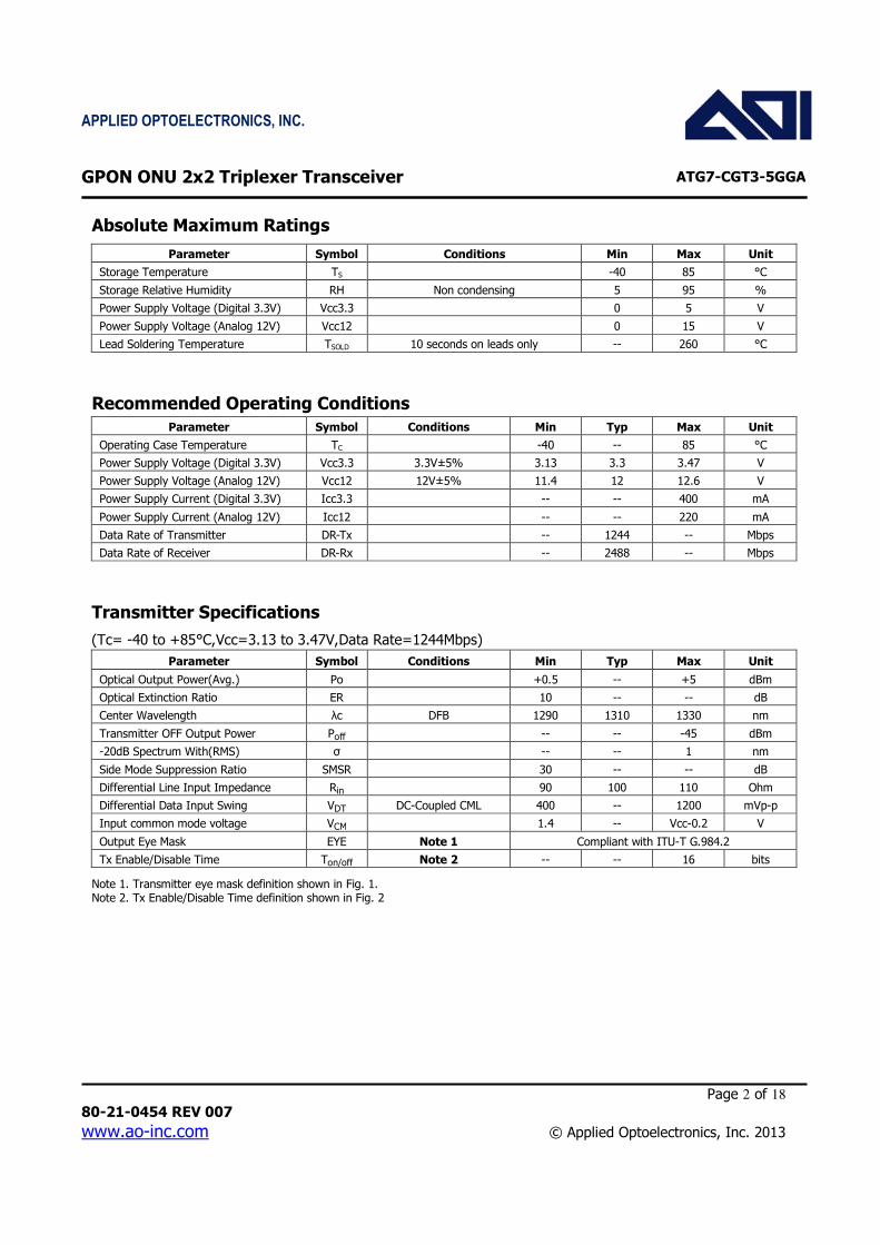
Absolute Maximum Ratings
Parameter Symbol Conditions Min Max Unit
Storage Temperature TS -40 85 °C
Storage Relative Humidity RH Non condensing 5 95 %
Power Supply Voltage (Digital 3.3V) Vcc3.3 0 5 V
Power Supply Voltage (Analog 12V) Vcc12 0 15 V
Lead Soldering Temperature TSOLD 10 seconds on leads only -- 260 °C
Recommended Operating Conditions
Parameter Symbol Conditions Min Typ Max Unit
Operating Case Temperature TC -40 -- 85 °C
Power Supply Voltage (Digital 3.3V) Vcc3.3 3.3V±5% 3.13 3.3 3.47 V
Power Supply Voltage (Analog 12V) Vcc12 12V±5% 11.4 12 12.6 V
Power Supply Current (Digital 3.3V) Icc3.3 -- -- 400 mA
Power Supply Current (Analog 12V) Icc12 -- -- 220 mA
Data Rate of Transmitter DR-Tx -- 1244 -- Mbps
Data Rate of Receiver DR-Rx -- 2488 -- Mbps
Transmitter Specifications
(Tc= -40 to +85°C,Vcc=3.13 to 3.47V,Data Rate=1244Mbps) Parameter Symbol Conditions Min Typ Max Unit
Optical Output Power(Avg.) Po +0.5 -- +5 dBm
Optical Extinction Ratio ER 10 -- -- dB
Center Wavelength λc DFB 1290 1310 1330 nm
Transmitter OFF Output Power Poff -- -- -45 dBm
-20dB Spectrum With(RMS) σ -- -- 1 nm
Side Mode Suppression Ratio SMSR 30 -- -- dB
Differential Line Input Impedance Rin 90 100 110 Ohm
Differential Data Input Swing VDT DC-Coupled CML 400 -- 1200 mVp-p
Input common mode voltage VCM 1.4 -- Vcc-0.2 V
Output Eye Mask EYE Note 1 Compliant with ITU-T G.984.2
Tx Enable/Disable Time Ton/off Note 2 -- -- 16 bits
Note 1. Transmitter eye mask definition shown in Fig. 1. Note 2. Tx Enable/Disable Time definition shown in Fig. 2

ATG7-CGT3-5GGA
APPLIED OPTOELECTRONICS, INC.
GPON ONU 2x2 Triplexer Transceiver
Page 3 of 18
80-21-0454 REV 007
www.ao-inc.com © Applied Optoelectronics, Inc. 2013
h
1244.16 Mbit/s x1/x4 0.22/0.78 x2/x3 0.40/0.60 y1/y4 0.17/0.83 y2/y3 0.20/0.80
Figure-1 Eye Mask Diagram and Setup
Figure-2 Ton/Toff Time Definition

ATG7-CGT3-5GGA
APPLIED OPTOELECTRONICS, INC.
GPON ONU 2x2 Triplexer Transceiver
Page 4 of 18
80-21-0454 REV 007
www.ao-inc.com © Applied Optoelectronics, Inc. 2013
Receiver Specification
(Tc= -40 to +85°C,Vcc=3.13 to 3.47V,Data Rate=2488Mbps)
Parameter Symbol Conditions Min Typ Max Unit
Input Optical Wavelength λ APD 1480 1490 1500 Nm
Receiver Sensitivity PINMIN Note 1 -- -- -28 dBm
Input Saturation Power (Overload) PINMAX -8 -- -- dBm
Signal Detect- Assert PA -- -- -28 dBm
Signal Detect- De-Assert PD -45 -- -- dBm
Signal Detect-Hysteresis PA- PD 0.5 -- -- dB
Differential Data Output Swing VDO AC-Coupled CML 400 -- 1200 mVp-p
Signal Detect Output Voltage-High VSDH LVTTL
2.4 -- Vcc V
Signal Detect Output Voltage-Low VSDL 0 -- 0.4 V
Note 1. Measured with PRBS 223 –1 at 10-10 BER
Specification of RF Video Receiver
Parameter Symbol Conditions Min Typ Max Unit
Operating Wavelength -- 1550 1555 1560 nm
Receiving Optical Power (Avg.) -- -7 -- +1 dBm
RF AGC Dynamic Range -- 24 -- -- dB
Responsivity -- 0.9 -- -- mA/mW
RF Output Level -- Note 1 20 -- -- dBmV/ch
Total RF Output power -- -- 36 -- dBmV
RF Output Impedance -- -- 75 -- Ω
CNR -- Note 2 46 -- -- dB
C/CSO -- Note 3 -- -- -55 dB
C/CTB -- -- -- -55 dB
RF Return Loss -- 46-870MHz -- -- -12 dB
RF Output Tilt -- 46-870MHz 2 4 6 dB
RF Output Flatness -- 46-870MHz -- -- 3.0 dB
Note 1: Tested at 450MHz, OMI=4.4% per channel, RF_Setting=0 Note 2: Tested at -7dBm, 78 channels in 46M~870M, OMI=3.5% per channel Note 3: Test at +1dBm, 78channels in 46M~870M, OMI=3.5% per channel

ATG7-CGT3-5GGA
APPLIED OPTOELECTRONICS, INC.
GPON ONU 2x2 Triplexer Transceiver
Page 5 of 18
80-21-0454 REV 007
www.ao-inc.com © Applied Optoelectronics, Inc. 2013
Functional Block Diagram
Optical Characteristics
Parameter Conditions Min Typ Max Unit
Optical Isolation From external 1310 nm to 1490 nm Rx 28 -- -- dB
Optical Isolation From external 1310 nm to 1555 nm Rx 40 -- -- dB
Optical Cross-talk From internal 1310 nm to 1490 nm Rx -- -- -47 dB
Optical Cross-talk From internal 1310 nm to 1555 nm Rx -- -- -47 dB
Optical Isolation From external 1555 nm to 1490 nm Rx 35 -- -- dB
Optical Isolation From external 1490 nm to 1555 nm Rx 35 -- -- dB
Optical Return Loss (Reflectance) 1480 nm to 1500 nm -- -- -30 dB
Optical Return Loss (Reflectance) 1260 nm to 1360 nm -- -- -30 dB

ATG7-CGT3-5GGA
APPLIED OPTOELECTRONICS, INC.
GPON ONU 2x2 Triplexer Transceiver
Page 6 of 18
80-21-0454 REV 007
www.ao-inc.com © Applied Optoelectronics, Inc. 2013
Pigtail Fibre Characteristics
Parameter Min Typ Max Unit Note
Mode Field Diameter 9 µm
Cladding Diameter 125 µm
Jacket Diameter 0.9 mm
Bending Radius of Pigtail Fiber 30 mm
Tension Force on Pigtail Fiber 1 Kg
Pigtail Fiber Length 590 ±12 mm
Optical Return Loss (APC type)- 1310nm 55 dB
Digital Diagnostic Monitor Accuracy
Parameter Accuracy Unit Calibration Note
Transceiver Temperature ±3°C °C Internal Operating Temp.(Tc)
Digital Power Supply Voltage ±3% V Internal Vcc=3.3V±5%
TX Bias Current ±10% mA Internal Specified by nominal bias value
1490nm RX Optical Power ±3dB dBm Internal -28 to -8 dBm
RF output power ±3dB dBmv Internal 20~50dBmV (Total Power)
1550nm Rx Optical Power ±3dB dBm Internal -7 to +1dBm
Note. Temperature and Voltage is measured internal to the transceiver.
ATG7-CGT3-5GGA
APPLIED OPTOELECTRONICS, INC.
GPON ONU 2x2 Triplexer Transceiver
Page 7 of 18
80-21-0454 REV 007
www.ao-inc.com © Applied Optoelectronics, Inc. 2013
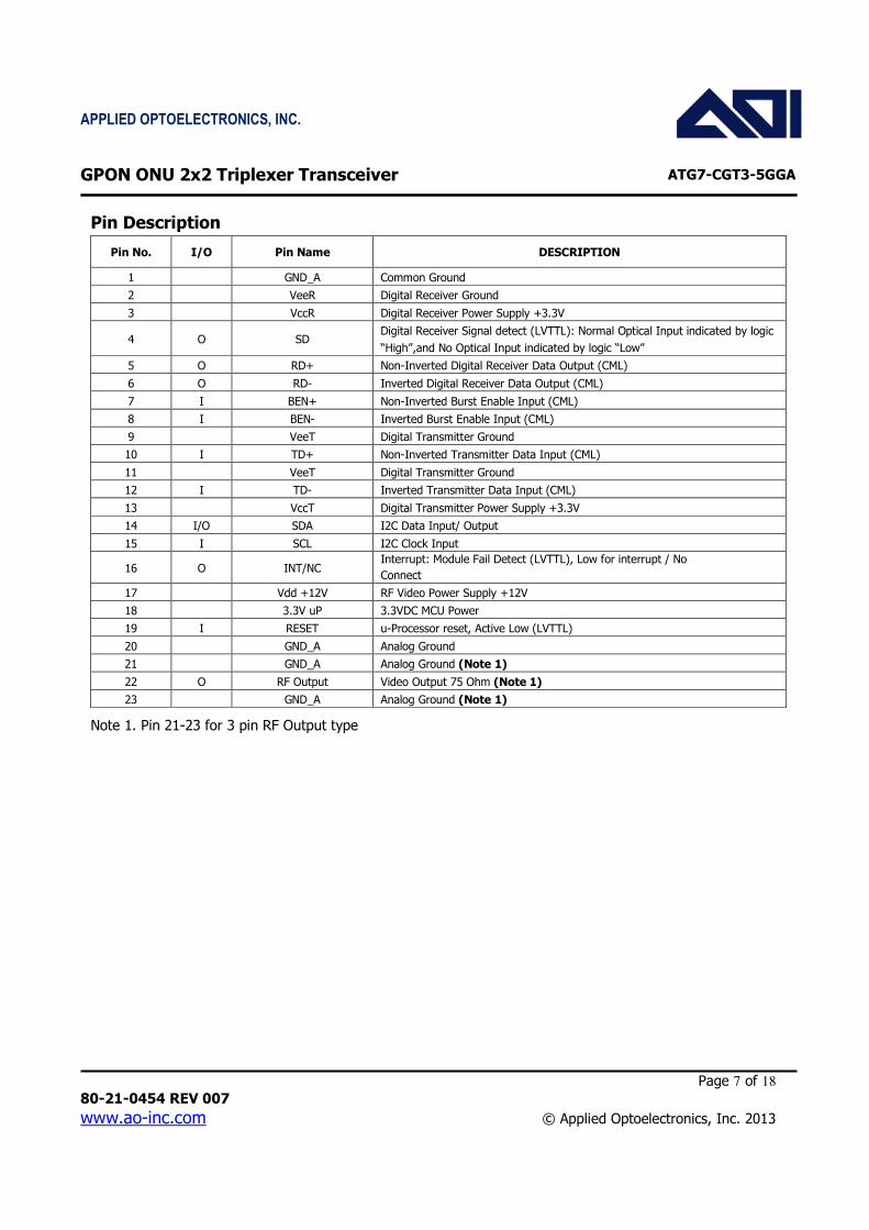
Pin Description
Pin No. I/O Pin Name DESCRIPTION
1 GND_A Common Ground
2 VeeR Digital Receiver Ground
3 VccR Digital Receiver Power Supply +3.3V
4 O SD Digital Receiver Signal detect (LVTTL): Normal Optical Input indicated by logic
“High”,and No Optical Input indicated by logic “Low”
5 O RD+ Non-Inverted Digital Receiver Data Output (CML)
6 O RD- Inverted Digital Receiver Data Output (CML)
7 I BEN+ Non-Inverted Burst Enable Input (CML)
8 I BEN- Inverted Burst Enable Input (CML)
9 VeeT Digital Transmitter Ground
10 I TD+ Non-Inverted Transmitter Data Input (CML)
11 VeeT Digital Transmitter Ground
12 I TD- Inverted Transmitter Data Input (CML)
13 VccT Digital Transmitter Power Supply +3.3V
14 I/O SDA I2C Data Input/ Output
15 I SCL I2C Clock Input
16 O INT/NC Interrupt: Module Fail Detect (LVTTL), Low for interrupt / No
Connect
17 Vdd +12V RF Video Power Supply +12V
18 3.3V uP 3.3VDC MCU Power
19 I RESET u-Processor reset, Active Low (LVTTL)
20 GND_A Analog Ground
21 GND_A Analog Ground (Note 1)
22 O RF Output Video Output 75 Ohm (Note 1)
23 GND_A Analog Ground (Note 1)
Note 1. Pin 21-23 for 3 pin RF Output type
ATG7-CGT3-5GGA
APPLIED OPTOELECTRONICS, INC.
GPON ONU 2x2 Triplexer Transceiver
Page 8 of 18
80-21-0454 REV 007
www.ao-inc.com © Applied Optoelectronics, Inc. 2013
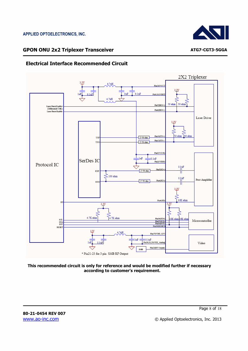
Electrical Interface Recommended Circuit
This recommended circuit is only for reference and would be modified further if necessary according to customer’s requirement.

ATG7-CGT3-5GGA
APPLIED OPTOELECTRONICS, INC.
GPON ONU 2x2 Triplexer Transceiver
Page 9 of 18
80-21-0454 REV 007
www.ao-inc.com © Applied Optoelectronics, Inc. 2013
Mechanical Design Diagram
UNIT: mm [inch]

ATG7-CGT3-5GGA
APPLIED OPTOELECTRONICS, INC.
GPON ONU 2x2 Triplexer Transceiver
Page 10 of 18
80-21-0454 REV 007
www.ao-inc.com © Applied Optoelectronics, Inc. 2013
EEPROMSerial ID Memory Contents (A0h) Address Name of field Hex Description
BASE ID FIELDS
00-11 Customer Part Number (ASCII) 20,20,20,20,20,20,20,20,20,20,20,20
12 BR, Upstream (unit:10Mbps) 7C 1240Mbps
13 BR, Downstream (unit:10Mbps) F8 2480Mbps
14-15 Reserved 00,00,
16 Minimum RF output level (Note1) 01 20dBmV
17 Low Video Input Power (unit: 0.1dBm) BA -7dBm
18 High Video Input Power (unit: 0.1dBm) 0A +1dBm
19 Nominal RF Tilt (unit: 0.1dB) 28 +4dB (from 55-870MHz)
20-35 Vendor name (ASCII) 41,4F,49,20,20,20,20,20,20,20,20,20,20,20,20,20 AOI
36 Reserved 0
37 RF Bandwidth (Note2) 01 46MHz to 870MHz
38-49 Reserved 00,00,00,00,00,00,00,00,00,00,00,00,
50 Video PD Responsivity (Unit: 0.01mA/mW) 5A 0.9 mA/mW
51-55 Reserved 00,00,00,00,00,
56-59 Vendor Rev (ASCII) 41,20,20,20, A
60 Digital TX Wavelength (Units: 10nm) 83 1310nm
61 Digital RX Wavelength (Units: 10nm) 95 1490nm
62-67 Reserved 00,00,
68-83 Vendor SN (ASCII) xx,xx,xx,xx,xx,xx,xx,xx,xx,xx,xx,xx,xx,xx,xx,xx
84-91 Manufacturing Date code (ASCII) xx,xx,xx,xx,xx,xx,20,20, (YY/MM/DD/BB)
92 Diagnostic Monitoring Type (Note3) 28
93-95 Reserved 00,00,00,
96-125 Vendor PN (ASCII) 41,54,47,37,2D,43,47,54,33,2D,35,47,47,41,20, 20,20,20,20,20,20,20,20,20,20,20,20,20,20,20
ATG7-CGT3-5GGA
126-127 Vendor Specific 00,00,

ATG7-CGT3-5GGA
APPLIED OPTOELECTRONICS, INC.
GPON ONU 2x2 Triplexer Transceiver
Page 11 of 18
80-21-0454 REV 007
www.ao-inc.com © Applied Optoelectronics, Inc. 2013
Note.1
Byte Value RF(dBmV) Freq(MHz) OMI(%) Loading Condition Carrier Type
1 20 450 4.4 78 Analog Modulated
Note.2
Byte Value Min. RF (MHz) Max. RF (MHz)
1 46 870
Note.3
Data Address
(Dec) Bits Description Setting
92 7 Reserved for legacy diagnostic implementations. Must be '0' for compliance with this document
0
92 6 Digital diagnostic monitoring implemented per SFF-8472 0
92 5 Internally Calibrated 1
92 4 Externally Calibrated 0
92 3 Received power measurement type, 0-OMA, 1 =Average Power
1
92 2 1 =Address change required. 0= not required. SEE SFF-8472 for "addressing modes change".
0
92 1 Reserved 0
92 0 Reserved 0

ATG7-CGT3-5GGA
APPLIED OPTOELECTRONICS, INC.
GPON ONU 2x2 Triplexer Transceiver
Page 12 of 18
80-21-0454 REV 007
www.ao-inc.com © Applied Optoelectronics, Inc. 2013
EEPROMSerial ID Memory Contents (A2h) Address Name of field Hex Description
BASE ID FIELDS
00-01 Temp High Alarm Tc(Max.)+10 (1LSB=1/256)
02-03 Temp Low Alarm Tc(Min.)-5 (1LSB=1/256)
04-05 Temp High Warning Tc(Max.)+5 (1LSB=1/256)
06-07 Temp Low Warning Tc(Min.) (1LSB=1/256)
08-09 Voltage High Alarm Vcc+10% (1LSB=100uV)
10-11 Voltage Low Alarm Vcc-10% (1LSB=100uV)
12-13 Voltage High Warning Vcc+6% (1LSB=100uV)
14-15 Voltage Low Warning Vcc-6% (1LSB=100uV)
16-17 1550nm RX Power High Alarm
18-19 1550nm RX Power Low Alarm
20-21 1550nm RX Power High Warning
22-23 1550nm RX Power Low Warning
24-25 RF Power High Alarm
26-27 RF Power Low Alarm
28-29 RF Power High Warning
30-31 RF Power Low Warning
32-33 1490nm RX Power High Alarm
34-35 1490nm RX Power Low Alarm
36-37 1490nm RX Power High Warning
38-39 1490nm RX Power Low Warning
40 Bias High Alarm (1LSB=1mA)
41 Bias Low Alarm (1LSB=1mA)
42-43
44-45
46-47
48-49
50 RF_Offset
Control of the RF output level to offset for different OMI values in feed forward or different channel plans in feed back (LSB=0.5dB)

ATG7-CGT3-5GGA
APPLIED OPTOELECTRONICS, INC.
GPON ONU 2x2 Triplexer Transceiver
Page 13 of 18
80-21-0454 REV 007
www.ao-inc.com © Applied Optoelectronics, Inc. 2013
51-55 Reserved 00,00,00,00,00 Reserved
56-59 Rx_PWR (4)
20,20,20,20 Set to zero for “internally calibrated” devices.
60-63 Rx_PWR (3)
20,20,20,20 Set to zero for “internally calibrated” devices.
64-67 Rx_PWR (2)
20,20,20,20 Set to zero for “internally calibrated” devices.
68-71 Rx_PWR (1)
3F,80,20,20 Set to 1 for “internally calibrated” devices.
72-75 Rx_PWR (0)
20,20,20,20 Set to zero for “internally calibrated” devices.
76-88 Reserved 20,20,20,20,20,20,20,20,20,20,20,20,20 Reserved
89-90 Reserved 00,00 Reserved
91-92 Reserved 00,00 Reserved
93-94 Version 00,01 Firmware version number
95 Reserved 00 Reserved
96-97 Temperature (MSB, LSB) Internally measured module temperature (1LSB=1/256)
98-99 Supply Voltage (MSB, LSB)
Internally measured supply voltage in pin 18 of the module(microprocessor Supply) Convert Signed 16-bit value to decimal Vcc = X*0.1mV
100-101 1550nm RX Power (MSB, LSB)
Monitor of current from the PD across 300ohm resistor; To calculate the value: VPDMON(dBm)= 10*log((VPD_AD/Rkohm/1023*1.1)/(Resp/100)); -VPD_AD = (A2[100]*256+A2[101]); -Rkohm = 0.3; -Resp = A0[50];
102-103 RF Power (MSB, LSB) Measured Rx output power RF POWER(dBmV) = (A2[102]*256+A2[103])*0.1-60
104-105 1490nm RX Power (MSB, LSB)
Internally measured supply voltage in pin 18 of the module(microprocessor Supply) Convert Signed 16-bit value to decimal 10*log(((A2[104]*256+A2[105])*0.1)/1000)
106-107
108 TX Bias Current Internally measured Tx Bias current, multiply by 1.0 to get the DC bias current. (Unit=1mA)
109 Reserved 00 Reserved
110 Control Bit Note.1
111
112 Alarm Flag Bit Note.3
113 Flag Bit Note.4
114 IMASK0 Interrupt Mask for Byte 70 (0= enable)

ATG7-CGT3-5GGA
APPLIED OPTOELECTRONICS, INC.
GPON ONU 2x2 Triplexer Transceiver
Page 14 of 18
80-21-0454 REV 007
www.ao-inc.com © Applied Optoelectronics, Inc. 2013
115 IMASK1 Interrupt Mask for Byte 71 (0= enable)
116 Flag Warning Flag Bit Note.5
117 Flag Bit Note.6
118 IMASK2 Interrupt Mask for Byte 74 (0= enable)
119 IMASK3 Interrupt Mask for Byte 75 (0= enable)
120 Control Bit Note.7
121-122 Reserved 00,00 Reserved
123 Password Byte 3 High order byte of 32 bit password
124 Password Byte 2 Second highest order byte of 32 bit password
125 Password Byte 1 Second lowest order byte of 32 bit password
126 Password Byte 0 Low order byte of 32 bit password
127 User EEPROM Select “1” selects user writable EEPROM at locations 128-255
128-255 Reserved 00 Reserved for future use
Note.1 Control Bit
Data Address
(Dec) Bits Bytes Name of Field Description
110
7
1
RF_SQUELCH_EN Control bit. If set, allows RF squelching if input power too low
6 Reserved Reserved
5 HOLD_AGC Control bit. If set, hole AGC fixed. Auto-clears on boot
4 TX Disable Control "1"=Tx output Disable, "0"= Tx output enable
3 RF Output Enable "1"=RF Output Enable, "0"=RF Output Disable
2 TX_FAULT "0"=Digital state of the TX Fault Output Pin
1 Interrupt "1"=Interrupt
0 Signal Detect State "1"=Digital state of the SD Output Pin.
Note.3 Alarm Flag Bit
Data Address
(Dec) Bits # Bytes Name of Field Description
112
7
1
RF Power Low Alarm Set when RF Power is below low alarm level.
6 RF Power High Alarm Set when RF Power exceeds high alarm level.
5 1550nm RX Power Low Alarm Set when 1550nm Received Power is below low alarm level.
4 1550nm RX Power High Alarm Set when 1550nm Received Power exceeds high alarm level.
3 Vcc Low Alarm Set when internal supply voltage is below low alarm level.
2 Vcc High Alarm Set when internal supply voltage exceeds high alarm level.
1 Temp Low Alarm Set when internal temperature is below low alarm level.
0 Temp High Alarm Set when internal temperature exceeds high alarm level.
Note.4 Flag Bit

ATG7-CGT3-5GGA
APPLIED OPTOELECTRONICS, INC.
GPON ONU 2x2 Triplexer Transceiver
Page 15 of 18
80-21-0454 REV 007
www.ao-inc.com © Applied Optoelectronics, Inc. 2013
Data Address
(Dec) Bits # Bytes Name of Field Description
113
7
1
TX Disable State_ON TX_DIS went HIGH
6 TX Disable State_OFF TX_DIS went LOW
5 TX_FAULTL_ON TxFail signal went HIGH
4 TX_FAULT_OFF TxFail signal went LOW
3 Signal Detect_ON SD signal went HIGH
2 Signal Detect_OFF SD signal went LOW
1 1490nm RX Power Low Alarm Set when 1490nm Received Power is below low alarm level.
0 1490nm RX Power High Alarm Set when 1490nm Received Power exceeds high alarm level.
Note.5 Flag Warning Flag Bit
Data Address
(Dec) Bits # Bytes Name of Field Description
116
7
1
RF Power Low Warning Set when RF Power is below low warning level.
6 RF Power High Warning Set when RF Power exceeds high warning level.
5 1550nm RX Power Low Warning Set when 1550nm Received Power is below low warning level.
4 1550nm RX Power High Warning Set when 1550nm Received Power exceeds high warning level.
3 Vcc Low Warning Set when internal supply voltage is below low warning level.
2 Vcc High Warning Set when internal supply voltage exceeds high warning level.
1 Temp Low Warning Set when internal temperature is below low warning level.
0 Temp High Warning Set when internal temperature exceeds high warning level.
Note.6 Flag Bit
Data Address
(Dec) Bits # Bytes Name of Field Description
117
7
1
RESET STATE Reset Interrupt Status. 1 if reset was performed (occurs at each power up). This is the only interrupt that cannot be masked.
6
5
4
3 TX Bias Low Alarm Set when TX Bias current is below low alarm level.
2 TX Bias High Alarm Set when TX Bias current exceeds high alarm level.
1 1490nm RX Power Low Warning Set when 1490nm Received Power is below low warning level.
0 1490nm RX Power High Warning Set when 1490nm Received Power exceeds high warning level.
Note.7 Control Bit
Data Address
(Dec) Bits # Bytes Name of Field Description
120
7
1 Reserved Reserved 6
5
4
3

ATG7-CGT3-5GGA
APPLIED OPTOELECTRONICS, INC.
GPON ONU 2x2 Triplexer Transceiver
Page 16 of 18
80-21-0454 REV 007
www.ao-inc.com © Applied Optoelectronics, Inc. 2013
2
1 Reset (Write 1 to reset) Reset (Write 1 to reset)
0 Save Active data to Flash (write 1) Save Active data to Flash (write 1)

ATG7-CGT3-5GGA
APPLIED OPTOELECTRONICS, INC.
GPON ONU 2x2 Triplexer Transceiver
Page 17 of 18
80-21-0454 REV 007
www.ao-inc.com © Applied Optoelectronics, Inc. 2013
Label drawing
Unit: mm

ATG7-CGT3-5GGA
APPLIED OPTOELECTRONICS, INC.
GPON ONU 2x2 Triplexer Transceiver
Page 18 of 18
80-21-0454 REV 007
www.ao-inc.com © Applied Optoelectronics, Inc. 2013
Regulatory Compliance
Item Standard
Electromagnetic
Interference (EMI)
FCC Part 15 Class B
EN55022 Class B (CISPR 22B)
VCCI Class B
Electrostatic Discharge to the Electrical Pins (ESD)
MIL-STD-883E Method 3015.7
Electrostatic Discharge to the
Receptacle (ESD) IEC 61000-4-2
RoHS 2011/65/EU
Laser Eye Safety FDA 21CFR 1040.10 and 1040.11
Component Recognition UL and TUV
Laser Safety Information
All versions of this laser are Class 1 laser products per IEC1/EN2 60825-1:2007. Users should observe safety precautions such as those recommended by ANSI3 Z136.1-2000, ANSI Z36.2-1997 and IEC 60825-1:2007.
This product conforms to FDA (CDRH) 21 CFR 1040.10 and 1040.11 except for deviations of laser safety class designation
pursuant to 'Laser Notice No.50' , dated June 24, 2007
Product labeling:
If labeling is not affixed to the module due to size constraints; then rather, labeling is placed on the outside of the
shipping box.
This product is not shipped with a power supply.
Caution: use of controls or adjustments or performance of procedures other than those specified herein may result in hazardous radiation exposure.
Certifications
UL 60950-1 (E243407)
TUV EN60950-1/A12:2011, EN 60825-1, EN 60825-2
Documentation is available upon request.
(1) IEC is a registered trademark of the International Electrotechnical Commission
(2) Within Europe the IEC standard has been adopted as a European Normative standard known as EN 60825, and each European country will have its own
version of this standard, for example, the British Standards version known as BS EN 60825. There can be small differences between the different countries versions of EN 60825, and these are in part caused by the process of translating the standard into the native language of that country.
(3) ANSI is a registered trademark of the American National Standards Institute
Note : All information contained in this document is subject to change without notice.
Class 1 Laser Product Compliance with 21 CFR 1040.10 and 1040.11