GOOD PRACTICE BOOKLET - Europa
36
For FP7 Semiconductor Design Research GOOD PRACTICE BOOKLET
Transcript of GOOD PRACTICE BOOKLET - Europa

Fo
r F
P7
S
em
ic
on
du
cto
r D
esig
n R
ese
arc
h
GOOD PRACTICE BOOKLET


Authors: Gergana Hristozova, inno Svetlana Klessova, inno Franck le Gall, inno Anna Pyatenko, Fraunhofer IIS Giles Brandon, Intelligentsia Copyright © 2010 SEMIDEC project consortium.
Disclaimer The opinions, figures and estimates set forth in this publication are the responsibility of the authors, and should not necessarily be considered as reflecting the views or carrying the endorsement of the European Commission. The designations used and the presentation of the material in this publication do not imply the expression of any opinion whatsoever on the part of the European Commission, concerning the legal status of any country, territory, city or area, or of its authorities, or concerning the delimitation of its frontiers or boundaries. Mention of firm names and commercial products does not imply the endorsement of the European Commission.

TABLE OF CONTENTS
ABBREVIATIONS ......................................................................................................................1
INTRODUCTION ......................................................................................................................2
ABOUT THE SEMIDEC PROJECT ..........................................................................................................2
WHAT IS THIS BOOKLET ABOUT? ..........................................................................................................2
WHO SHOULD READ THIS BOOKLET? .....................................................................................................2
HOW COULD THIS BOOKLET BE HELPFUL? ..............................................................................................2
1. FP7- AN OPPORTUNITY FOR RUSSIAN SEMICONDUCTOR ORGANISATIONS ..............................3
1.1. ABOUT FP7 ...........................................................................................................................3
WHAT IS FP7? .............................................................................................................................3
FP7 COOPERATION PROGRAMME ...................................................................................................3
THEME 3 INFORMATION & COMMUNICATION TECHNOLOGIES (ICT) .....................................................4
EU RESEARCH “FUNDING SCHEMES” ................................................................................................4
1.2. RESEARCH PRIORITIES IN THE FIELD OF SEMICONDUCTOR DESIGN AND TOOLS (CHALLENGE 3) .............5
CHALLENGE 3. COMPONENT, SYSTEMS AND ENGINEERING ...................................................................5
EU KEY DESIGN RESEARCH PRIORITIES ...............................................................................................6
1.3. PARTICIPATION IN FP7, SUCCESSFUL PARTNERS SEARCH AND OTHER ON-GOING PROJECTS .................6
2. MORE ABOUT THE SEMICONDUCTOR DESIGN RESEARCH… ...................................................9
3. MAJOR EUROPEAN SEMICONDUCTOR DESIGN ORGANISATIONS AND KEY DETAILS ................. 11
4. WHAT ARE THE GOOD PRACTICES TO FOLLOW? ............................................................... 15
STEP 1: GET INVOLVED IN AN FP7 CONSORTIUM AND/OR FIND PARTNERS ............................................... 16
INCREASE YOUR VISIBILITY ............................................................................................................ 16
EMPHASIZE YOUR COMPETENCIES ................................................................................................. 17
UTILISE YOUR NETWORK .............................................................................................................. 18
STEP 2: INCREASE YOUR CHANCES OF SUCCESS FOR SUCCESSFUL PROPOSAL SUBMISSION ..................... 19
ESTIMATE YOUR CHANCES OF SUCCESS ACCURATELY ......................................................................... 19
BE SURE YOU ARE MOTIVATED ENOUGH TO SPEND TIME ON AND GIVE A LOT OF EFFORT TO PROPOSAL PREPARATION
............................................................................................................................................... 19
EXPOSE THE ADDED VALUE OF YOUR IDEA CLEARLY ........................................................................... 19
BE SURE TO MEET THE REQUIREMENTS OF THE EUROPEAN COMMISSION ............................................. 20
STEP 3: SUCCEED IN THE PROJECT NEGOTIATION PHASE ........................................................................ 22
UNDERSTAND THE ADMINISTRATIVE REQUIREMENTS OF THE EC ............................................ 23
DEFINE INTELLECTUAL PROPERTY RIGHTS ........................................................................................ 23
STEP 4: CARRY OUT YOUR PROJECT EFFICIENTLY ................................................................................... 24
ENSURE QUALITY OF MANAGEMENT AND COORDINATION ................................................................. 24
ADAPT THE PROJECT TO THE ENVIRONMENT ................................................................................... 25
OVERCOME CULTURAL DIFFERENCES .............................................................................................. 25
COMMUNICATE EFFICIENTLY BY E-MAIL .......................................................................................... 26
STEP 5: DIFFUSE YOUR SCIENTIFIC RESEARCH AND ENSURE TECHNOLOGY TRANSFER ................................... 28
EMPHASIZE THE VALUE OF YOUR WORK.......................................................................................... 28
GET INTEGRATED INTO EUROPEAN NETWORKS ............................................................................... 29
5. CONCLUSION ............................................................................................................. 30
6. BIBLIOGRAPHY ....................................................................................................... 31

SEMIDEC GOOD PRACTICE BOOKLET | Abbreviations 1
ABBREVIATIONS
EC – European Commission
EU – European Union
SD – Semiconductor Design
RU - Russian
FP7 – 7th Framework Programme
ICT - Information and Communication Technologies
PC – Project Coordinator
PO – Project Officer

SEMIDEC GOOD PRACTICE BOOKLET | Introduction 2
INTRODUCTION
ABOUT THE SEMIDEC PROJECT
The SEMIDEC Project “Stimulating Semiconductor Design Cooperation between Europe and Russia” (www.semidec-ru.eu) is supported by the European Commission to explore new opportunities and to stimulate cooperation in the field of Semiconductor Design (SD) research between the EU and Russia. Consequently, SEMIDEC aims to develop cooperation in semiconductor design and tools that are relevant to the research priorities, identified in the FP7 ICT Work Programme 2009 and ENIAC Strategic Research Agenda 2007.
WHAT IS THIS BOOKLET ABOUT?
The present booklet has been prepared by the SEMIDEC project team in order to help beginners in FP7 research projects acquire a greater chance of success during all the phases of preparation and implementation of FP7 Semiconductor related projects. The booklet highlights various good practices, which represent knowledge or ways of doing things that are cited as examples. The guide has been developed in consultation with FP7 project managers, SD researchers, experts and consultants who have extensive experience in the implementation of FP7 semiconductor design projects. The summary of good practices reflects direct observations from FP7 projects. Good practices are illustrated with short examples of case studies, which allow for a better understanding of the ideas highlighted.
WHO SHOULD READ THIS BOOKLET?
The booklet has been in particular designed for Russian SD research organizations who are interested in participating in FP7 projects, but who do not know where to start.
HOW COULD THIS BOOKLET BE HELPFUL?
Organized into three main chapters, the booklet contains a wide range of useful information for implementing semiconductor design projects. In the first chapter, Russian researchers will be shown step by step some good practices, which could facilitate their understanding of FP7 projects preparation, submission, implementation and management. The booklet offers sets of tips, according to the phase, which could be helpful to beginners The SEMIDEC project team hopes that by sharing detected best practices in the field of Semiconductor Design, research in the area will be improved and the chances of success within the Russian semiconductor R&D communities will be increased.

SEMIDEC GOOD PRACTICE BOOKLET | FP7- An opportunity for Russian Semiconductor Organisations 3
1. FP7- AN OPPORTUNITY FOR RUSSIAN SEMICONDUCTOR ORGANISATIONS
1.1. ABOUT FP7
WHAT IS FP7?
The Seventh EU Framework Programme for research and Technological Development (FP7) is the European Union’s principal instrument for European science and technology development. The EU aims to “make Europe the most competitive and dynamic knowledge-based economy in the world, capable of sustainable economic growth, create better and even more jobs and greater social cohesion”. The FP7’s final objective is the creation of the European Research Area (ERA). Since their launch in 1984, the Framework Programmes have played a leading role in multidisciplinary research and cooperative activities for European member states and associated countries. The FP7 has run since 2007 and will continue up until 2013. With a budget of 53.2 billion Euros over its 7 years lifespan, it is the largest European funding programme to this day. Four Specific Programmes are organized to reach the goals: Cooperation, Ideas, People and Capacities.
FP7 COOPERATION PROGRAMME
The Cooperation Programme is designed to meet its specific goal, namely “gaining leadership in key scientific and technology areas”. It supports all types of collaborative research activities among European partners. Therefore the research activities in the field of semiconductors are funded under the Cooperation Programme, which can be considered as the core of FP7 with the € 32,413 million budget allocated by the EU. The Programme is spread into 1O different research themes, related to the major fields in science and research of EU interest. It is intended to facilitate and support pan-European public-private partnerships and the coordination and synergies of national research programmes through international cooperation. Among these themes, the most relevant for the semiconductor sector is Theme 3 “Information & Communication Technologies (ICT)”. In theory, a defined research theme is independent but allows joint activities across the themes at the same time. That is why the research priorities for semiconductor design methods and tools are identified in the FP7 ICT Work Programme 2009 as well as ENIAC Strategic Research Agenda 2007. The ENIAC Joint Technology Initiative (JTI) is a European public-private partnership on nanoelectronics, which is under the Theme 4 “Nanosciences, nanotechnologies, materials & new production technologies”. The ENIAC aims to combine efforts of industry, EU Member States, associated states and the European Commission in the field.

SEMIDEC GOOD PRACTICE BOOKLET | FP7- An opportunity for Russian Semiconductor Organisations 4
THEME 3 INFORMATION & COMMUNICATION TECHNOLOGIES (ICT)
The ICT theme is one of the FP7 key thematic areas representing 6-8% of the European GDP. With a total budget of € 9,050 million, the research on ICT is structured around seven “Challenges”:
Challenge 1: Pervasive and Trusted Network and Service Infrastructures Challenge 2: Cognitive systems, interaction, robotics Challenge 3: Components, systems, engineering Challenge 4: Digital Libraries and Content Challenge 5: Towards sustainable and personalized healthcare Challenge 6: ICT for mobility, environment sustainability Challenge 7: Independent living, inclusion and participatory governance
The main objectives of the ICT Work Programme is to foster frontier research of future and emerging technologies that will give Europe the agility to react to new ideas and opportunities; enhance the participation in FP7 ICT support international collaboration; and maximize the impact of existing European research projects.
EU RESEARCH “FUNDING SCHEMES”
Collaborative Projects (CP) aim to generate new knowledge, including new technology, or common resources for research applicable in terms of development or improvement of products, processes, services or policy. There are two types of CPs:
Specific Targeted Research Projects (STREPs) This scheme finances 1 to 2 years of small or medium scaled projects with a specific and defined research objective and which could implement technological R&D, demonstration and project management activities.
Integrating Projects (IPs) IPs concerns larger scale actions running from 3 to 5 years. A comprehensive “programme” approach includes a coherent integrated set of activities: R&D activities, demonstration, protection and dissemination of knowledge, project management and setting‐up. There is some flexibility to adapt the project compared with STREPs.
Networks of Excellence (NoE) are designed for research organizations willing to combine and
functionally integrate a substantial part of their activities and capacities in a given field, in order to create a European “virtual research centre” in this field.
Coordination and Support Actions (CSA) coordinate or support research activities and policies. Two types of CSAs implement specific measures, such as networking, exchanges, transnational access to research infrastructures, studies, conferences, etc.
CSA Coordination Actions (CSA-CA) coordinate or create a network between other research actions for a specific purpose over a given time.

SEMIDEC GOOD PRACTICE BOOKLET | FP7- An opportunity for Russian Semiconductor Organisations 5
CSA Support Actions (CSA-SA) contribute to the implementation of the FPs, preparation of future Community research and technological development policy, the development of synergies with other policies, the stimulation, encouragement and facilitation of SME participation, civil society organizations and their networks, small research teams and newly developed or remote research centres in the activities of the thematic areas of the Cooperation programme and the setting up of research-intensive clusters across the EU regions.
FP7 funding scheme Minimum No of
participants
Typical No of
participants
Typical duration
Typical funding
Collaborative Projects
(CPs)
Specific Targeted Research Projects
(STREPs)
3 4-8 2-3 years 1-4 M€
Integrating Projects (IPs)
3 8-20 3-5 years 4-25 M€
Networks of Excellence (NoEs) 3 6-20 4 years 2-8 M€
Coordination & Support
Actions (CSAs)
Coordination Actions (CAs)
3 3-6 1-3 years 0.5-2 M€
Support Actions (SAs)
1 3-6 1-3 years 0.5-2 M€
The good practices illustrated in the present booklet are however not only relevant for FP7 funded research projects. They could also be applied in the framework of other sources of funding such as JTI (Joint Technology Initiatives), EUREKA, EEN (Enterprise Europe Network), CIP (Competitiveness and Innovation Framework programme) etc.
1.2. RESEARCH PRIORITIES IN THE FIELD OF SEMICONDUCTOR DESIGN AND TOOLS (CHALLENGE 3)
CHALLENGE 3. COMPONENT, SYSTEMS AND ENGINEERING
Challenge 3 aims to support industry and European academy research in the strategic sectors such as micro and nano systems and to assure that theses new technologies satisfy the European economy and society’s needs. In each Challenge, there are precise research areas called “Objectives”, identified in a 10 year time frame. Objectives provide more details on the framework of research to be carried out and proposals should be submitted under these objectives. For the implementation of each workprogamme a number of ‘Calls for Proposal’ is defined setting the time plan for research proposals to be submitted.

SEMIDEC GOOD PRACTICE BOOKLET | FP7- An opportunity for Russian Semiconductor Organisations 6
Strategic objectives addressed for Challenge 3 in the FP7-ICT Calls for Proposals (2009-2010)
3.1 Nanoelectronics Technology 3.2 Design of Semiconductor 3.3 Flexible, Organic and Large Area Electronics 3.4 Embedded Systems Design 3.5 Engineering of Networked Monitoring and Control Systems 3.6 Computing Systems 3.7 Photonics 3.8 Organic Photonics and other Disruptive Photonics Technologies 3.9 Microsystems and Smart Miniaturized Systems
EU KEY DESIGN RESEARCH PRIORITIES
According to the FP7 ICT Work Programme 2009 and ENIAC Strategic Research Agenda 2007, Europe’s key priorities for semiconductor design methods and tools include the following 8 research activities:
Design of energy efficient electronic systems, and thermal effect aware design;
Integration of heterogeneous functions: 3D, System-in-Package and Network-on-Chip;
Methods for reuse of IP blocks, test and verification;
Design platforms and interfaces for mixed/new technologies;
New paradigms for design of reliable circuits with less reliable devices;
Reliability-aware design including EMR/EMC requirements;
Design for manufacturability taking into account increased variability of new processes;
Better modeling of devices at all design levels into circuit/system design
1.3. PARTICIPATION IN FP7, SUCCESSFUL PARTNERS SEARCH AND OTHER ON-GOING PROJECTS
Overview of general participation in FP7 (semiconductor design thematic),
The sphere of the FP7 interests is very wide in the area of semiconductor design. Its focus reflects different technology trends: miniaturisation and increased performance, addition of new functionalities, mastering system complexity, new nano-electronic devices, photonics and organic electronics; and covers such directions as actuators and embedded computational and intelligent elements; very advanced nano-electronic components; integration of smart components and smart systems; embedded systems and cooperative monitoring and control; and flexible, organic and large area electronics and photonics.
SEMIDEC GOOD PRACTICE BOOKLET | FP7- An opportunity for Russian Semiconductor Organisations 7
On-going projects in the field of semiconductor
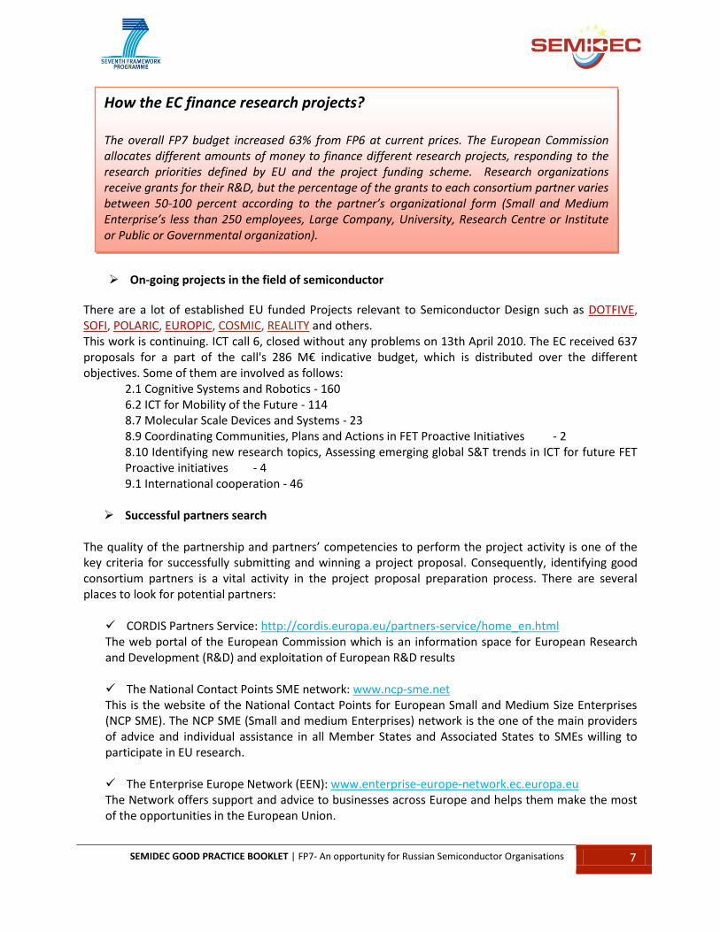
There are a lot of established EU funded Projects relevant to Semiconductor Design such as DOTFIVE, SOFI, POLARIC, EUROPIC, COSMIC, REALITY and others. This work is continuing. ICT call 6, closed without any problems on 13th April 2010. The EC received 637 proposals for a part of the call's 286 M€ indicative budget, which is distributed over the different objectives. Some of them are involved as follows:
2.1 Cognitive Systems and Robotics - 160 6.2 ICT for Mobility of the Future - 114 8.7 Molecular Scale Devices and Systems - 23 8.9 Coordinating Communities, Plans and Actions in FET Proactive Initiatives - 2 8.10 Identifying new research topics, Assessing emerging global S&T trends in ICT for future FET Proactive initiatives - 4 9.1 International cooperation - 46
Successful partners search The quality of the partnership and partners’ competencies to perform the project activity is one of the key criteria for successfully submitting and winning a project proposal. Consequently, identifying good consortium partners is a vital activity in the project proposal preparation process. There are several places to look for potential partners:
CORDIS Partners Service: http://cordis.europa.eu/partners-service/home_en.html The web portal of the European Commission which is an information space for European Research and Development (R&D) and exploitation of European R&D results The National Contact Points SME network: www.ncp-sme.net This is the website of the National Contact Points for European Small and Medium Size Enterprises (NCP SME). The NCP SME (Small and medium Enterprises) network is the one of the main providers of advice and individual assistance in all Member States and Associated States to SMEs willing to participate in EU research. The Enterprise Europe Network (EEN): www.enterprise-europe-network.ec.europa.eu The Network offers support and advice to businesses across Europe and helps them make the most of the opportunities in the European Union.
How the EC finance research projects? The overall FP7 budget increased 63% from FP6 at current prices. The European Commission allocates different amounts of money to finance different research projects, responding to the research priorities defined by EU and the project funding scheme. Research organizations receive grants for their R&D, but the percentage of the grants to each consortium partner varies between 50‐100 percent according to the partner’s organizational form (Small and Medium Enterprise’s less than 250 employees, Large Company, University, Research Centre or Institute or Public or Governmental organization).

SEMIDEC GOOD PRACTICE BOOKLET | FP7- An opportunity for Russian Semiconductor Organisations 8
EECA competence platform: www.eeca-ict.eu The Competence Platform is an online service offered through the EU – EECA Gateway on ICT research and development portal. You can use it to promote your ICT competences and to find information about your potential partners - ICT experts and organizations of the EECA region and Europe. IDEAL-IST project: www.ideal-ist.net Web-based platform and useful tool for joining ICT projects, finding partners for your project idea and finding services to support you in your ICT project within the Seventh European Framework Programme.

SEMIDEC GOOD PRACTICE BOOKLET | More about the Semiconductor Design Research… 9
2. MORE ABOUT THE SEMICONDUCTOR DESIGN RESEARCH…
Microelectronics is everywhere around us in everyday life. Now we are going into micro and nanosystems, which combine sensors and actuators, mechanical structures and electronics to receive information from the environment and react to it. Moreover, as movable and flexible parts are often used in systems, the role of mechanics - or rather micromechanics – rises in electronics. New technologies, new materials, new designs are developing very rapidly. The dominant electronics trend is towards what is called Ambient Intelligence. It is a wide area for Semiconductor R&D activities.
These are some of the following application areas where semiconductor devices can be used:
Automotive Electronics
Computer Platforms
Computer Peripherals
Consumer Electronics
Industrial electronics
Medical Electronics
Military/Aerospace Electronics
Power
Wireless Communications
Wired communications However, as SD are “pervasive”, these application areas mentioned above are just several from many other examples. Furthermore, the applications of SD become larger with the development of the “internet of things”. A variety of technologies and semiconductor segments can be used to enable Ambient Intelligence environments such as:
Total Semiconductor
Total IC
Memory IC (DRAM, SRAM, Flash)
Microcomponent IC (MPU, MCU)
Logic IC (PLD/FPGA, ASIC)
Analog IC (Amplifier, Voltage, Data Convertors)
Discrete (RF and Microwave, Power transistors)
Optical Semiconductors (LEDs, Laser Diodes, Sensors)
Sensors and Actuators.
The key factor in microelectronics is miniaturization. In 1965 Gordon Moore made his famous observation that the number of transistors, on a given area of a semiconductor chip, will double every year. Moore revised his law in 1975 – increasing the period of doubling to 1.5-2 years, which, in practice, still applies today. The press called this statement ‘Moore's Law’. Moore’s law has been extended to micro-systems with the “More than Moore’s” concept. It is ‘More functions on a chip’ instead of ‘More transistors per square mm’. “More than Moore” explores a new area of micro/nanoelectronics, which goes beyond the boundaries of conventional semiconductor technologies and applications, creating and integrating various non-digital functionality to

SEMIDEC GOOD PRACTICE BOOKLET | More about the Semiconductor Design Research… 10
semiconductor products. “More than Moore” focuses on creating high value micro/nanoelectronics systems, motivating new technological possibilities and unlimited application potential. Semiconductor design research is possible because of the establishment of the semiconductor industry. It is the aggregate collection of companies engaged in the design and fabrication of semiconductor devices. There are:
semiconductor companies, specialising in the design and sale of hardware devices and semiconductor chips (not in production though).
semiconductor fabrication plants (commonly called fabs), factories where semiconductor devices such as integrated circuits are manufactured,
integrated device manufacturers (IDM), semiconductor companies which design, manufactures, and sell integrated circuit (IC) products,
original design manufacturers (ODM), companies which design and manufacture a product which is specified and eventually branded by another firm for sale and
original equipment manufacturers, or OEM, manufacture products or components that are purchased by a company and retailed under the purchasing company's brand name, among them.
The SD R&D area is marked by intense rivalries between individual companies. There is always pressure on chip makers to come up with something better, faster and cheaper. This pressure extends to chip makers, foundries, design labs and distributors – everyone connected to the business of bringing chips from R&D into high-tech equipment. The result is an industry that continually produces cutting-edge technology.

SEMIDEC GOOD PRACTICE BOOKLET | Major European Semiconductor Design Organisations and key details 11
3. MAJOR EUROPEAN SEMICONDUCTOR DESIGN ORGANISATIONS AND KEY DETAILS
The current section identifies some of the major organizations involved in semiconductors design. Most of the organizations listed here are members of the European Semiconductor Industry Association (ESIA). In addition, some of the organisations are also presented in the JRS report “The Future of Semiconductor Intellectual Property Architectural Blocks in Europe”, 2009 (see Bibliography, page 30).
Organisation Name Type Web Site Short description Position on the value chain
ARM http://www.arm.com/ ARM designs the technology that lays at the heart of advanced digital products, from wireless, networking and consumer entertainment solutions to imaging, automotive, security and storage devices. The ARM comprehensive product offering includes 32-bit RISC microprocessors, graphics processors, enabling software, cell libraries, embedded memories, high-speed connectivity products, peripherals and development tools. Combined with comprehensive design services, training, support and maintenance, and the company’s broad Partner community, they provide a total system solution that offers a fast, reliable path to market for leading electronics companies. The organization participates in FP7 projects (e.g. REALITY).
IP Blocks licensing
Motorola http://www.motorola.com Motorola has heritage which is rich in communications and electronics industry innovation. The company has a wide range products portfolio, covering devices producing, networks, systems and different services. The organization participates in FP7 projects (e.g. E3 project).
IP Blocks licensing
CEVA (Parthus, DSP Group)
http://www.ceva-dsp.com/index.php
CEVA is a leading licensor of silicon intellectual property (SIP) platform solutions and DSP cores for mobile handset, consumer electronics and storage applications. CEVA's IP portfolio includes comprehensive solutions for multimedia, audio, voice over packet (VoP), Bluetooth and Serial ATA (SATA), and a wide range of programmable DSP cores and subsystems with different price/performance metrics serving multiple markets.
IP Blocks licensing
Imagination Technologies
http://www.imgtec.com/ Imagination Technologies Group plc is an international leader in the creation and licensing of semiconductor System-on-Chip Intellectual Property (SoC IP) and in the development and manufacture of DAB digital and connected radios.
IP Blocks licensing (SoC IP)
Synopsys http://www.synopsys.com/IP/Pages/default.aspx
Synopsys is the leading provider of high-quality, silicon-proven IP solutions for SoC designs. The broad DesignWare® IP portfolio includes complete interface IP solutions consisting of controllers, PHY and verification IP for widely used protocols, analog IP, embedded memories, logic libraries, configurable CPU/DSP cores and SoC infrastructure IP. In addition, Synopsys offers SystemC transaction-level models to build virtual prototypes for rapid, pre-silicon development of software. With a robust IP development methodology, reuse tools, extensive investment in quality and comprehensive technical support, Synopsys enables
IP Blocks licensing Design tools

SEMIDEC GOOD PRACTICE BOOKLET | Major European Semiconductor Design Organisations and key details 12
designers to accelerate time-to-market and reduce integration risk. Synopsys participates in FP7 projects(e.g. ATEMOX)
Wipro-Newlogic http://www.newlogic.com Wipro-NewLogic offers besides its broad system IP portfolio also an impressive range of IC Design and IP Integration services with a team of about 350 engineers. The organisation offers SoC development, which includes multiprocessor designs e.g. for wireless Baseband/Application processors; RF development e.g WiMAX, UWB, WLAN, GSM; Analog Designs; Mixed Signal Designs.
IP Blocks licensing Design service
Dolphin Integration http://www.dolphin.fr/ Dolphin Integration is up to their charter as the most adaptive and lasting creator in the Microelectronics Design Industry to "enable mixed signal Systems-on-Chip". Three additional competency centers: Design for MEMS in Duisburg, Germany, since 1997, Design of Power Regulators in Montreal, Canada, since 2007, Design of Scatted Memories in Netanya, Israel, since 2009.Dolphin participates in FP7 projects, such as MACROS, MNENEE and many others.
IP Blocks licensing Design service
Silicon Image http://www.siliconimage.com/
Silicon Image is the leader in high-speed serial communications IC designs for the consumer electronics, PC and display, and storage solution markets. As the pioneer and market leader of the popular DVI and HDMI® standards and an innovator and driver of the SATA interface, Silicon Image has shipped more than 100 million standards-based semiconductors.
IP Blocks licensing Design service
Intel Europe http://www.intel.com/ Intel Labs Europe (ILE) is a network of Research & Development, Product, and Innovation Labs spanning the European region as well as variety of Intel business units. ILE was formally established in early 2009 as a central means of coordinating activities across Intel’s diverse network of labs and to further strengthen Intel’s commitment to and alignment with European R&D. In addition to driving key technology innovations for Intel, ILE works closely with academic, industry, and government institutions to advance innovations and strengthen Europe’s technology leadership in the global community. Intel participates in many different FP7 projects.
Global
EMEA Freescale Semiconductor
www.freescale.com The company supplies the "brains" for all kinds of automotive, consumer, industrial and networking applications. The portfolio of power management solutions, microprocessors, microcontrollers, sensors, radio frequency semiconductors, analog and mixed signal circuits and software technologies are embedded in products used around the world. The Freescale Semiconductor’s intellectual property portfolio contains more than 6,400 patent families. The company participates in FP7 projects.
Global
STMicroelectronics http://www.st.com/stonline/
The Group aims to offer multimedia convergence solutions and power applicatiions. It has a portfolio of different technologies, such as High performance logic and derivates, BCD, Embedded non-volatile memory. The company participates in FP7 projects (e.g.NANOCMOS).
Global
Cadence http://www.cadence.com Cadence Design Systems, Inc. laid out a new vision for the semiconductor industry, EDA360. In outlining an application-driven approach to system design and development, Cadence issued a challenge to the semiconductor and electronic design automation (EDA)
Design tools
SEMIDEC GOOD PRACTICE BOOKLET | Major European Semiconductor Design Organisations and key details 13
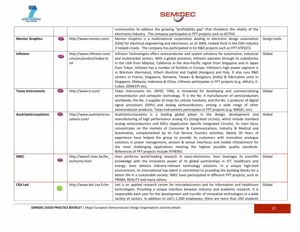
communities to address the growing “profitability gap” that threatens the vitality of the electronics industry. The company participates in FP7 projects such as ACTIVE.
Mentor Graphics http://www.mentor.com/ Mentor Graphics is a multinational corporation dealing in electronic design automation (EDA) for electrical engineering and electronics, as of 2004, ranked third in the EDA industry it helped create. The company has participated in EU R&D projects such as FP7 ATESST2.
Design tools
Infineon http://www.infineon.com/cms/en/product/index.html
Infineon Technologies offers semiconductor and system solutions for automotive, industrial and multimarket sectors. With a global presence, Infineon operates through its subsidiaries in the USA from Milpitas, California in the Asia-Pacific region from Singapore and in Japan from Tokyo. Infineon has a number of facilities in Europe. Infineon's high power segment is in Warstein (Germany), Villach (Austria) and Cegléd (Hungary) and Italy. It also runs R&D centers in France, Singapore, Romania, Taiwan & Bengaluru (India) & fabrication units in Singapore, Malaysia, Indonesia & China. Infineon participates in FP7 projects (e.g. eMuCo, E-Cubes, GENESYS etc).
Global
Texas Instruments http://www.ti.com/ Texas Instruments Inc. (NYSE: TXN), is renowned for developing and commercializing semiconductor and computer technology. TI is the No. 4 manufacturer of semiconductors worldwide, the No. 2 supplier of chips for cellular handsets, and the No. 1 producer of digital signal processors (DSPs) and analog semiconductors, among a wide range of other semiconductor products. Texas Instruments participates in FP7 projects (e.g. MAGIC, etc).
Global
Austriamicrosystems http://www.austriamicrosystems.com/
Austriamicrosystems is a leading global player in the design, development and manufacturing of high performance analog ICs (integrated circuits), which include standard analog semiconductors and ASICs (Application Specific Integrated Circuits). Its main focus concentrates on the markets of Consumer & Communications, Industry & Medical and Automotive, complemented by its Full Service Foundry activities. Nearly 30 Years of experience have helped the group to provide its customers with innovative analogue solutions in power management, sensors & sensor interfaces and mobile infotainment for the most challenging applications meeting the highest possible quality standards. References of FP7 projects include ATHENIS.
Global
IMEC http://www2.imec.be/be_en/home.html
Imec performs world-leading research in nano-electronics. Imec leverages its scientific knowledge with the innovative power of its global partnerships in ICT, healthcare and energy. Imec delivers industry-relevant technology solutions. In a unique high-tech environment, its international top talent is committed to providing the building blocks for a better life in a sustainable society. IMEC have participated in different FP7 projects, such as PRIMA, REALITY and many others.
Global
CEA Leti http://www-leti.cea.fr/en Leti is an applied research center for microelectronics and for information and healthcare technologies. Providing a unique interface between industry and academic research, it is responsible each year for the development and transfer of innovative technologies in a wide variety of sectors. In addition to Leti’s 1,500 employees, there are more than 250 students
Global

SEMIDEC GOOD PRACTICE BOOKLET | Major European Semiconductor Design Organisations and key details 14
Type of organistion: Industry EC initiative R&D organisations
The list of organisations, working in the field of semiconductors design research, is not exhaustive. There are also many EU universities and R&D centers with teams working in that field. More information about relevant teams and laboratories, with research related to semiconductors, is available on the following link: http://www.semiconductors.co.uk/research_laboratories/europe-eu_k-to-z.htm
involved in research activities, which makes Leti a mainspring of innovation expertise. Leti’s portfolio of 1,500 families of patents helps strengthen the competitiveness of its industrial partners. References of FP7 projects include MAGIC, SURPASS, PHYDYAS.
Fraunhofer IIS http://www.iis.fraunhofer.de/en/index.jsp
The Fraunhofer Institute for Integrated Circuits IIS performs contract research and development for industry and public authorities. Headed by the collegial board of directors, Professor Dr.-Ing. Heinz Gerhäuser (Executive Director) and Professor Dr.-Ing. Günter Elst, Fraunhofer IIS researchers develop microelectronic systems and devices along with the required integrated circuits and software. References of FP7 projects include ATHENIS, RAPTOR, EMILI.
Global
Europractice http://www.europractice-ic.com/index.php
Europractice was launched by the European Commission (DGIII) in October 1995 to help companies improve their competitive position in world markets by adopting ASIC, Multi-Chip Module (MCM) or Microsystems solutions in the products they manufacture. The program helps to reduce the perceived risks and costs associated with these technologies by offering potential users a range of services, including initial advice and ongoing support, reduced entry costs and a clear route to chip manufacture and product supply. Europractice can also provide users with the training and CAD software required to design and develop their ASIC, MCM or Microsystems solution.
Support
SEMIDEC GOOD PRACTICE BOOKLET | What are the good practices to follow? 15
4. WHAT ARE THE GOOD PRACTICES TO FOLLOW?
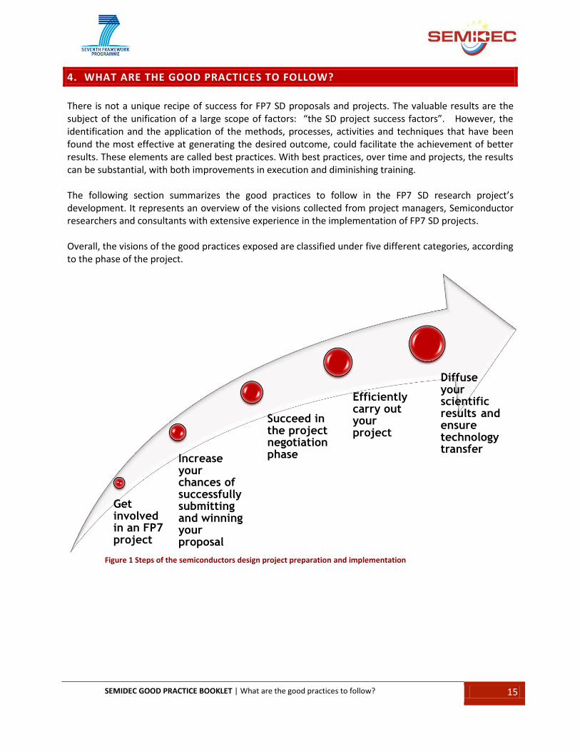
There is not a unique recipe of success for FP7 SD proposals and projects. The valuable results are the subject of the unification of a large scope of factors: “the SD project success factors”. However, the identification and the application of the methods, processes, activities and techniques that have been found the most effective at generating the desired outcome, could facilitate the achievement of better results. These elements are called best practices. With best practices, over time and projects, the results can be substantial, with both improvements in execution and diminishing training. The following section summarizes the good practices to follow in the FP7 SD research project’s development. It represents an overview of the visions collected from project managers, Semiconductor researchers and consultants with extensive experience in the implementation of FP7 SD projects. Overall, the visions of the good practices exposed are classified under five different categories, according to the phase of the project.
Figure 1 Steps of the semiconductors design project preparation and implementation
Get involved in an FP7 project
Increase your chances of successfully submitting and winning your proposal
Succeed in the project negotiation phase
Efficiently carry out your project
Diffuse your scientific results and ensure technology transfer

SEMIDEC GOOD PRACTICE BOOKLET | What are the good practices to follow? 16
STEP 1: GET INVOLVED IN AN FP7 CONSORTIUM AND/OR FIND PARTNERS
When you start thinking of preparing proposals and apply for funding under FP7, you should take into consideration the fact that the development of an SD project requires the pooling of competencies, skills, experience and funds, rarely found together in single organizations. One of the options for overcoming the lack of all these elements is to get involved in a consortium or to find complementary partners. In order to help you make this first step, you should consider increasing your visibility, emphasizing your competencies and utilising your network.
INCREASE YOUR VISIBILITY
If you have never participated in European collaborative research, it is certainly difficult to demonstrate your capabilities to EU partners. A good starting point to increase your visibility is to participate in relevant research events. Go to conferences, consultation workshops, etc. which are key networking places among participants for future initiatives. There are also the networking events of the ICT conferences as well as info-days on Framework Programmes (at local/regional, national or European level) organized by the EC, EU-funded support actions, etc. Such events offer face-to-face meetings with representatives of the EC and key organizations which have been participating in EU funded programmes. Talk about your recent research and promote your competencies to them.
Get Started in FP7 research projects (e.g. having participated once, it is easier to find and to be found by partners)
As for many things in the everyday life, the most difficult step is beginning. The situation is the same for the European research projects. Once you have started, things become easier: you have learned how to do things, you become well known, you find partners more easily and you manage and implement your project more efficiently.
Case Study 1: ISPRAS (Institute of system programming of RAS) started to participate in EU projects, when the Russian institute team was invited to join the Go4It consortium in 2005. Since this moment, ISPRAS showed to other international FP7 experienced organizations its motivation and willingness to participate in EU cooperative projects. In addition, the good start allowed ISPRAS to receive invitations for other FP7 projects, such as ISTOK.Ru and its successor ISTOK-SOYUZ. In the framework of ISTOK.Ru project, ISPRAS representatives took part in the ICT 2008. There they were provided the opportunity to network with EC representatives, EU partners and thus to increase their visibility. Today, the ISPRAS team is not only known among EU FP7 participants, but has also qualified personal to provide FP7 trainings.

SEMIDEC GOOD PRACTICE BOOKLET | What are the good practices to follow? 17
EMPHASIZE YOUR COMPETENCIES
Despite your efforts to participate in the events listed above, it would be useless if you do not know how to “sell yourself”.
Analyze your strengths and weakness Knowing yourself better is a very important task you should undertake before the project begins. Self-awareness helps self-motivation and goal setting. Some questions to ask yourself:
What are our capabilities today?
What do we want to achieve in the long run?
What is our ambition? (Whether you want to focus on a specific area and deepen your expertise, or open up to a larger spectrum of research areas? In which area?)
Having a clear objective (Time specific, measurable and controllable) motivates people and a detailed action plan allows you to see the progress you make. In a self-assessment, we often overestimate ourselves. Be sure that the targets you have set are within your reach and relevant to your competencies, know-how, experience, available resources, timescale, etc.
Create communication tools to give away (e.g. Team CV with your sales points)
Your team CV in the form of a leaflet should give an organizational background, members’ qualifications and the scope of work carried out. Make sure that it is not too loaded with detail; rather it sums up your main achievements and strengths. Your mission (a brief description of what you offer, to whom your work is targeted, etc.), specialty, vision, logo and contact details must be provided. You can also mention Grants/Awards, Talks and Publications, Key staff, Past work/projects, especially collaborative experiences (In this part, you can illustrate some of case studies from your portfolio and clients you have worked with. If any, their testimony can be added).
Initial Check List:
We are European leaders on a specific topic We want to enlarge our European cooperation
and support the competitiveness of our companies
We want to access new knowledge and best practices
We are ready to spend days in writing a proposal that may be lost
You speak English
Case Study 2 By promoting their strength in multiple beam interference lithography technology, the Institute of Applied Physics of the Russian Academy of Sciences (IAP) was able to participate in the 3 year FP6 project DELILA. The main aim of the 2m euro project was to develop new production technology for high resolution fabrication – better than 40nm - of 2D and 3D nanostructures and devices. With IAP’s support, the DELILA team was able to successfully fabricate high resolution nanostructures with feature sizes.

SEMIDEC GOOD PRACTICE BOOKLET | What are the good practices to follow? 18
UTILISE YOUR NETWORK
Your own contacts are, surprisingly, one of the best ways to search partners. Any acquaintances including former and existing clients, research/business partners, personal contacts, colleague contacts, etc. in either private sectors (commercial or non-lucrative organizations) or public areas (universities, authorities, etc.) could be your future partner. However, you should avoid choosing people or organizations just because you know them. You need partners and not friends. Your knowledge of their expertise for the required activities, their former experiences, their available resources, their reputation in the field, etc. should help you to evaluate them. The two main points you should assess are complementary competencies and possible synergies between organizations.
Case Study 3 Through personal contacts at Intelligentsia Consultants, the National Aerospace University of Ukraine "KhAI" has been presented to several European research partners for FP6 and FP7 projects. Recently, this has included introduction to the Centre for Integrated Electronic Systems and Biomedical Engineering, Tallinn University of Technology, which resulted in participation in an FP7 proposal dealing with dependable embedded systems for aerospace and medical applications.

SEMIDEC GOOD PRACTICE BOOKLET | What are the good practices to follow? 19
STEP 2: INCREASE YOUR CHANCES OF SUCCESS FOR SUCCESSFUL PROPOSAL SUBMISSION
ESTIMATE YOUR CHANCES OF SUCCESS ACCURATELY
Only a very small percentage (10-15%) of submitted proposals is retained for negotiations. Therefore, you should be prepared for some unsuccessful experiences. Take time to evaluate the elements of success and if your answers contain ‘No’, think again if it is worthwhile to continue the process, making a lot of effort and spending valuable time. At the same time, be aware that you can only learn from your errors and your own experience.
Does your idea fit into the research priorities/objectives of the field? Are you targeting an appropriate Call for proposals? (See above EU research “funding schemes”) Is the call deadline sufficient to prepare and submit a proposal? Is it technically feasible to carry out the project within the proposed budget? Will the number of expected proposals be high? Is your idea clearly formulated and is it understandable by others? Examine other issues such as specific call limitations and your particularities.
BE SURE YOU ARE MOTIVATED ENOUGH TO SPEND TIME ON AND GIVE A LOT OF EFFORT TO PROPOSAL PREPARATION
Preparing a proposal requires a significant amount of time and effort. Furthermore, if your proposal is not retained, then the time and effort you gave to writing the proposal will not be paid back. Even if the proposal comes to the negotiation phase, much time devoted would be financially unrewarded. Yet this is not like it comes to nothing. Proposal preparation could be the opportunity to widen your network and help you build experience. Encountered problems will teach you more than you would think and the social and professional circle built from the experience will indeed be valuable as you try to successfully submit a proposal again in the future. Before going forward, remember that collaboration is a process requiring commitment to work together.
EXPOSE THE ADDED VALUE OF YOUR IDEA CLEARLY
Your idea upon which your proposal is based is all that matters. What advances will your research make beyond the state-of-the-art? Does it create new knowledge? Or is it an innovative combination of existing technologies? One major and specific idea should be stressed and communicated throughout your proposal.

SEMIDEC GOOD PRACTICE BOOKLET | What are the good practices to follow? 20
BE SURE TO MEET THE REQUIREMENTS OF THE EUROPEAN COMMISSION
There are various criteria for each type of proposal (funding scheme) and for Call for Proposals that influence the overall quality of your proposal. First of all, the proposal structure must conform to the Commission guidelines provided (e.g. Guidelines for proposers). Bear in mind that the evaluators are not always experts nor native English speakers. Your message, therefore, should be addressed clearly in the proposal. Avoid complicated words and long sentences,
define terminology, abbreviations or acronyms of your scientific area and provide references if necessary. Diagrams and figures do help the better communication of ideas. Do not be afraid to repeat certain points to highlight your message. Also, to enhance your proposal quality, you should identify weak points and risks of your idea. Analyze them and add texts explaining how you intend to manage them to extenuate negative impacts. With regard to project methodology and management, present a schematic overview of the project and set milestones when major consortium decisions can be made about whether it is necessary to change some direction or not, which research tools to choose, how to proceed to the next work package, etc. Important project deliverables/results (reports, software, etc.) usually emerge before these milestones. The work proposed in the project is classified in specific work packages and each work package is divided into several tasks. In the proposal each partner
Case Study 4: One of the projects which have not been selected by the EC for support was the proposal “abORIGINAL”. The EC officers required that the idea was clearly exposed. While there was an extensive review of the state-of-the-art on the specific thematic Carbon Nanotubes, there was little concrete information on particular progress beyond it, especially on system level and for device concepts. The proposal did not contain sufficient details in design, fabrication and modeling of TFT devices and circuit building blocks. The assessment of technical risks and the respective contingency plans were inappropriate with respect to the ambitious goals of the proposal. The example shows that the added value and the idea should be exposed clearly.

SEMIDEC GOOD PRACTICE BOOKLET | What are the good practices to follow? 21
should be listed, and his work should be indicated, according to the specific rules of the EC. Furthermore, the proposal should offer actions, concerning dissemination, intellectual property and knowledge management. As for the budget, it should be balanced and coherent with the role, the size and the competency of each partner. Justification should be provided, detailing the relevant personnel and subcontracting costs. A financial plan and used resources will support the timetable all along the project. Last but not least, it is strongly recommended that your proposal discusses and proposes post-project exploitation of the research results. Researchers, those in non-profit institutions in particular, tend to think that research is purely research and nothing else should be taken into consideration. A further exploitation plan and/or R&D results dissemination/commercialization ideas after the end of your research project should however be proposed. Delivered results will contribute to development of e.g. new and/or improved products/services, processes, etc.
Case Study 5: The Walter project included the European Telecommunications Standards Institute (ETSI) in its consortium in order to ensure the full exploitation of standardization results. The project also included a specific task dedicated to networking activities which allowed for the signature of agreements with major institutions, working in the domain. As a result, WALTER has contributed to the modification of the EC regulatory landscape for radio spectrum allocation.

SEMIDEC GOOD PRACTICE BOOKLET | What are the good practices to follow? 22
STEP 3: SUCCEED IN THE PROJECT NEGOTIATION PHASE
The negotiation phase is intended to reach an agreement between the Commission and the Consortium on two aspects: the technical details of the project and financial and legal issues. This phase is crucial to prepare a Grant Agreement as well as for project management and reporting on the project execution.
After the evaluation, the EC will send the ‘Evaluation Summary Report (ESR)’ including useful feedback to the proposers. Proposals which passed all evaluation criteria are listed for funding and will be the subject of an ‘Invitation to Negotiations’ notification. Once starting the negotiation phase, it is worth noting that in every stage of the negotiation, the coordinator should respect the deadlines set by the EC. If a deadline is impossible to meet, you should inform the EC officer as early as possible and ask for an extension. The EC designates a Project Officer (PO) who will send the framework for negotiation to the Project Coordinator (PC). The framework contains in its annex all the requested actions and respective deadlines. The PC must provide different administrative documents and information requested by the European Commission. In addition, in most cases, different points such as the budget, tasks and timeframe are to be revised and modified. In order to succeed in the negotiation phase, the following good practices are to be considered:
- Take your time to understand clearly what the administrative requirements of the EC are - Define the Intellectual Property Rights in advance
End of the Evaluation
Evaluation Summary Report
Invitation to Negotiations
The framework for negotiation
Project contract preparation & Negotiations
Consortium Agreement
Grant Agreement
Project's
official start
The Negotiation Process

SEMIDEC GOOD PRACTICE BOOKLET | What are the good practices to follow? 23
UNDERSTAND THE ADMINISTRATIVE REQUIREMENTS OF THE EC One of the most important issues during the negotiation phase is to provide all the requested documents by the EC. For this purpose, the newcomers to EU research projects need to take their time to understand the procedures which can sometimes become complicated. A good practice to follow is to always read the Guidelines available on the EC Cordis website ( http://cordis.europa.eu/home_en.html).
DEFINE INTELLECTUAL PROPERTY RIGHTS Participants should prepare and sign a consortium agreement before the EC Grant Agreement enters into force. Since the latter sets out the basic legal requirements but not all details, it is recommended that the consortium agreement details the internal guidelines of different aspects of the project such as arrangements regarding the granting of specific access rights. Intellectual property (IP) issues are first and foremost to define in order to protect the idea and exploit the results. Another Consortium Agreement could be possibly drawn up later, amending the initial one according to the needs of participants and the evolution of the project. The Commission proposes the “Checklist for a Consortium Agreement” on its web site. http://cordis.europa.eu/fp7/find-doc_en.html In addition, in case of misunderstanding, CORDIS helpdesk is available: (Tel: +352 2929 42210
E-mail: [email protected] ) ( ftp://ftp.cordis.europa.eu/pub/fp7/docs/checklist_en.pdf )
Case Study 6: For the FP6 project SEMINANO involving the Moscow-based Surface Phenomena Research Group LLC, the main aim was to develop innovative production techniques, characterization and methods of application of semiconductor Nan crystals to light emitting devices and floating gate memories. Consequently, it was important that IP issues - concerning background and foreground knowledge - were clarified in a signed consortium agreement prior to the project start.
SEMIDEC GOOD PRACTICE BOOKLET | What are the good practices to follow? 24
STEP 4: CARRY OUT YOUR PROJECT EFFICIENTLY
ENSURE QUALITY OF MANAGEMENT AND COORDINATION
For effective Project Management and smooth project elaboration, there are several points you should bear in mind.
Project meetings management - Bring people together! Since project elaboration is a long term and continuous process, it is very important to create a team spirit in the consortium and everybody should enjoy working on the project. Official meetings, therefore, do not have to be too formal. Particularly, the Kick-off meeting offers the opportunity to all partners to have first face-to-face contacts and to get to know each other, which will establish trusting relationship. A relaxing environment and appreciation between participants can be created by these social activities, which will significantly help communication through the project duration. Face to face meetings and regular audio-conferences are crucial in this.
The importance of work division – Do what you can do better! The implementation phase is generally led by the project coordinator who is directly responsible for delivering all management reports to the European Commission with the support of project managers. His/her role is also to report on the project’s progress and supervise resources and budgets. If the technical manager is also handling the administrative and financial tasks of project coordination, he will be overloaded by everyday management and cannot be efficient. Two roles require completely different skills and none of the two should be underestimated. In this context, it is strongly recommended to assign a “Scientific or technical coordinator” –naturally an engineer or a scientist- and separate technical management from administrative one. They must be capable of assessing practical aspects of the project research and editing “Technical deliverables” with the support of the coordinator, instead of handling routines. To conclude, it is crucial to allocate the responsibilities to the right people who have already proven their proficiency in the field.
Management and coordination tools - Resort to the adequate tools! Quality of your project management and coordination can depend on what management tools you use and how you organize the work. Moreover, the reporting requirements of the Commission are rather complicated and detailed. Good reporting tools will facilitate the creation of reports with relatively low effort whilst ensuring good quality. The tools are also used for supervising the project budget and work performance. There are different management tools to do this. Establish a model of “action plan” assigning a responsible person to each task, timetable. Gantt diagram is a common technique used by a wide audience to illustrate a project schedule. It represents the start and finish dates of the phases and the dependency relationships between activities of a project.

SEMIDEC GOOD PRACTICE BOOKLET | What are the good practices to follow? 25
Here is a list from which you can choose a tool that can make your work easier: http://www.webdesignbooth.com/project-management-tools/.
Quality of deliverables and their on-time delivery – If a partner underperforms? In case of underperformance or bad performance of consortium partners, have an individual talk with the partners and find the reasons and solutions to the problem. If you have another partner who is capable of the work and willing to do it, think of redistributing responsibilities and changing the budget allocation. If the problem worsens or is repeated, then you should consider taking more serious measures, like finding new partners to replace underperforming partners.
ADAPT THE PROJECT TO THE ENVIRONMENT
The project should be reassessed and validated periodically to make necessary updates and adjustments. Always try to stay up to date and take advantage of “Progress meetings” and “External review” to discuss current issues throughout the project. The Commission and a number of external evaluators will attend the latter one in order to examine the project outcomes and to give advice on how to progress.
OVERCOME CULTURAL DIFFERENCES
People involved in the research come from different countries, cultures, educational systems, working environments and may also come from different domains and a cross-over of different disciplines. This makes international collaboration immeasurably wealthy but it is essential not to overlook how to cope with cultural differences. Once work begins, and especially if some of the partners are new to a European funded research, it is essential that all partners understand administrative and other practical issues of the mechanism. Asking
Case Study 7: The ISTOK-SOYUZ project, participated in by ICT R&D teams in five countries from Eastern Europe and Central Asia, including Russia, was funded by the EC under the conditions of involvement in the EECA cluster (www.eeeci-ict.eu). The three projects needed to adapt their strategy and approach in order to provide good quality services. The mid-term review of the project brought about the change in strategy of the three projects, in order to ensure better adaptation to the expanded environment. Better coordination between the three projects was established and new promotional branding was elaborated.

SEMIDEC GOOD PRACTICE BOOKLET | What are the good practices to follow? 26
questions is however not very spontaneous in some cultures. Be sure that questions are asked at the very start of the project and important issues clarified so that a common understanding of expectations and tasks can be built. Successful communication management within a multicultural team implies focusing on common objectives and forming an integrated entity beyond cultural differences. You should remind partners that there is “no magic wand” to overcome this and the best thing you can bring to the consortium is openness and respect. Yet here are some golden tips of intercultural team communication. Be patient with yourself and with others. Listen and be sensitive to other people’s thoughts and feelings. Do not prejudge through your knowledge the tendencies of other cultures. Learn about the individuals you are working with. Do not get emotional, stay calm and rational even if you do not understand. Diminish miscommunications by asking descriptive questions and by rephrasing what you have
understood to check it. Do not make a promise if you are not sure of keeping it. Make a simple and quick apology if you make a mistake.
COMMUNICATE EFFICIENTLY BY E-MAIL Despite email now being appreciated by everyone for its swiftness and convenience and considered as the main tool of communication in business, there is a growing concern amongst people about how to use it effectively and appropriately. People often write an email too casually with much less attention than should be taken, resulting in many misunderstandings. What you have written in an email cannot be taken back. Please consider it as if it were a public document, and avoid including exclusive information and/or statements carelessly. Here are a number of things to check before clicking the send button on your email.
Case Study 8: The management of international projects, including partners from different countries is always related to dealing with cultural differences. Projects like NESTER, ISTOK.Ru and many others showed that, Russian researchers are not regularly responding to each mail sent. However, if regular reminders by e-mails and phone are sent, the communication issues could be overcome. In addition, knowing that Russian partners are not native English speakers, the project manager is always supposed to explain clearly the instructions for the partners. That was the case of the projects NESTER, ISTOK.Ru and many others.
SEMIDEC GOOD PRACTICE BOOKLET | What are the good practices to follow? 27
Formality of the email: What type of relationship you have with the recipient? If the person is a formal business partner, you should treat an email like a business letter. In rather a casual relationship, the email can be more informal or even containing emoticons.
Avoid conflicts: Is the content appropriate to be discussed over email? Misinterpretations happen very easily in email communication due to a lack of nonverbal expressions we have in face-to-face communication. Some subjects are too sensitive that your intentions could be twisted and this can have serious consequences. When a conversation has turned into a conflict, it is best to suggest an end to the email exchange and to talk or meet in person.
Message title: Is your subject meaningful enough? Put enough information in the subject line so that the reader knows what your email is about and can prioritize it appropriately.
Sending documents: Are your attachments really necessary? Send them only if it is necessary and title the documents in a way that is easy for the recipient to find and sort once downloaded. Also, verify that they are not too big and that the receiver is able to open the attachment, especially with the recent formats such as docx, pptx etc.
Composing an email: Is your email clear and concise? Get straight to the point rather than start with small-talk. A long email often lacks focus and your reader can lose concentration. Use proper spelling, grammar and punctuation. Do spell check and read the message for errors before you send it. Remember that an email is a reflection of you and your organization.
Answering email: When did you receive the email? If there is no précised deadline, an email should be replied within 24 hours and preferably within the same working day. If you have other priorities or if you need more time to find what the sender wants, write a brief message back saying that you have received it and that you will get back to them as soon as possible. In European culture, it can even be considered rude if you do not answer the email.
Some other tips: o Keep the message thread: In business, we receive
so many emails a day that we cannot remember all discussions made before. Click “reply” instead of “new mail”.
o Include your sign-off and do not forget your international dialing code. o Be sparing with the high priority option and the Cc: field.

SEMIDEC GOOD PRACTICE BOOKLET | What are the good practices to follow? 28
STEP 5: DIFFUSE YOUR SCIENTIFIC RESEARCH AND ENSURE TECHNOLOGY TRANSFER
EMPHASIZE THE VALUE OF YOUR WORK
The European Commission considers showing and publishing the results of a project to the research community and making the acquired knowledge public very important. This is because partners will increase their research and industrial positions through “public” funding schemes. Thus, part of the acquired benefits must be transferred to the EU community. It is also beneficial for the consortium to assess the project impact on larger audience and to test the validity and relevance of a project’s results. In this way, peers and potential users will provide valuable feedback that could highlight possible improvements in the technical solutions that are proposed. Always think of dedicating some time during and after the project duration to disseminate or even commercialize your project research. This is however still not drawing scientists’ attention. Key results and findings from the project can be sold, switching it from public to private. Project partners should be ready to use and invest the outputs of the project. In order to do this, IPR issues and access rights should be discussed and defined accurately before finalizing the proposal and submitting it to the EC. Dissemination activities can be carried out through multiple channels:
Conferences and seminars presentations Workshops Exhibitions Thematic mailing lists Articles in scientific and professional journals and books Contribution to standards/open source implementations Collaboration with scenario and foresight development agencies, etc.
As a simple rule, every occasion is a valuable opportunity for talking about the project’s achievements. The most efficient way is taking part in conferences and workshops. A good practice is following up regularly the dates of the events you are interested in. Press communications and releases could be relevant if you want to access to the public at large. It is preferable to use a professional PR service when you deal with the press. However, you are not in control of what will be written by journalists. Thus, make sure to keep your message simple and clear. Do not get too ambitious in explaining technical aspects. Additional dissemination tools include the project Website, newsletters, posters and brochures.

SEMIDEC GOOD PRACTICE BOOKLET | What are the good practices to follow? 29
GET INTEGRATED INTO EUROPEAN NETWORKS
One of the good practices for SD research organizations to adopt is integration into European networks. There are European Technology Platforms (ETPs) and Networks of excellence (NoEs), which provide framework for stakeholders, researchers and interested parties to define research priorities and to improve research excellence. These two kinds of structures could present a good opportunity for semiconductor design organizations to ensure the application of their research. Joining an ETP and or NoEs could support the transition of Russian semiconductor design results towards businesses and markets that could also allow progressively moving the Russian semiconductor design sector, traditionally based on the fundamental research, towards applied research strongly oriented to market needs.
Case Study 9: For dissemination purposes, the Go4IT project team not only designed a simple web site but also developed an interactive web portal which served as a tool for on line discussions. In addition, the web site offers tools for software developers. The web-portal was available in English, Russian and Chinese. This established a useful communication channel for receiving important feedback from local Russian and Chinese users. Last but not least, the sustainability of the website was ensured beyond the end of the project. The project finished in 2008 and the web site is still active.
Case Study 10: The Institute of Semiconductors Physics of the National Academy of Sciences of Ukraine (ISP) is a member of the European platform for low-power applications on silicon-on-insulator technology (EUROSOI+). With the support of the European platform’s partners, ISP was able to organise the 6th International SemOI Workshop in April 2010 in Kyiv with the strong participation of leading European microelectonics organisations such as IMEC, CEA-LETI and STMicroelectronics. In turn, this is helping to stimulate further European research collaboration for ISP.

SEMIDEC GOOD PRACTICE BOOKLET | Conclusion 30
5. CONCLUSION
As you will have noticed, participating in a FP7 Programme certainly requires a considerable amount of time and effort. But it is not rocket science! Remember that the ideal project comes from good preparation and strong motivation. Many ‘Success Stories’ show a number of common good practices and highlight that by following the recommendations made in this booklet, semiconductor design research organizations will find it easier to avoid and overcome difficulties. The authors hope that this Booklet will help you determine the essential elements in composing a consortium and the demanding requirements in preparing proposals. By matching your project actions with the guidelines in this booklet, you could potentially ensure that all requirements are met appropriately at each stage. Thus, in following this booklet, the authors believe that it is very much possible to minimize the risks of project management and make sure that all valuable and innovative ideas obtain their expected results very successfully.
SEMIDEC GOOD PRACTICE BOOKLET | BIBLIOGRAPHY 31
6. BIBLIOGRAPHY
Other project publications
Training Guide “Getting Started with EU ICT Research”. 2009. SCUBE-ICT Project.
Catalogue of European Technology Platforms and Networks of Excellence. 2009. ISTOK-
SOYUZ Project
ENIAC Strategic research Agenda 2007
ICT Work Programme 2009
“The Future of Semiconductor Intellectual Property Architectural Blocks in Europe”, JRC,
2009
Web links:
http://cordis.europa.eu/fp7/home_en.html
http://cordis.europa.eu/technology-platforms/home_en.html
http://cordis.europa.eu/technology-platforms/pdf/eniac.pdf
http://cordis.europa.eu/fp7/ict/computing/includes/study.pdf
http://www.date-conference.com/date10/main/2010/find-edavillage-company
http://www.eeca.eu/