General Purpose, 16-Bit Flash Microcontrollers with...
338
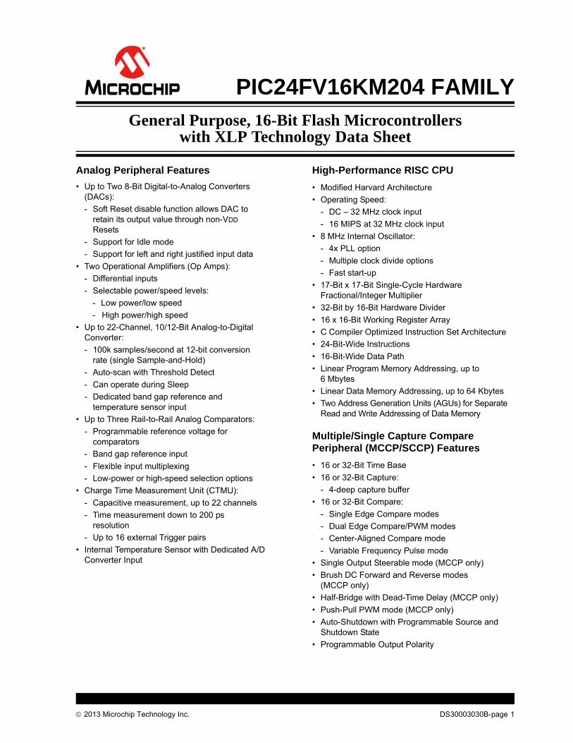
2013 Microchip Technology Inc. DS30003030B-page 1 PIC24FV16KM204 FAMILY Analog Peripheral Features • Up to Two 8-Bit Digital-to-Analog Converters (DACs): - Soft Reset disable function allows DAC to retain its output value through non-VDD Resets - Support for Idle mode - Support for left and right justified input data • Two Operational Amplifiers (Op Amps): - Differential inputs - Selectable power/speed levels: - Low power/low speed - High power/high speed • Up to 22-Channel, 10/12-Bit Analog-to-Digital Converter: - 100k samples/second at 12-bit conversion rate (single Sample-and-Hold) - Auto-scan with Threshold Detect - Can operate during Sleep - Dedicated band gap reference and temperature sensor input • Up to Three Rail-to-Rail Analog Comparators: - Programmable reference voltage for comparators - Band gap reference input - Flexible input multiplexing - Low-power or high-speed selection options • Charge Time Measurement Unit (CTMU): - Capacitive measurement, up to 22 channels - Time measurement down to 200 ps resolution - Up to 16 external Trigger pairs • Internal Temperature Sensor with Dedicated A/D Converter Input High-Performance RISC CPU • Modified Harvard Architecture • Operating Speed: - DC – 32 MHz clock input - 16 MIPS at 32 MHz clock input • 8 MHz Internal Oscillator: - 4x PLL option - Multiple clock divide options - Fast start-up • 17-Bit x 17-Bit Single-Cycle Hardware Fractional/Integer Multiplier • 32-Bit by 16-Bit Hardware Divider • 16 x 16-Bit Working Register Array • C Compiler Optimized Instruction Set Architecture • 24-Bit-Wide Instructions • 16-Bit-Wide Data Path • Linear Program Memory Addressing, up to 6 Mbytes • Linear Data Memory Addressing, up to 64 Kbytes • Two Address Generation Units (AGUs) for Separate Read and Write Addressing of Data Memory Multiple/Single Capture Compare Peripheral (MCCP/SCCP) Features • 16 or 32-Bit Time Base • 16 or 32-Bit Capture: - 4-deep capture buffer • 16 or 32-Bit Compare: - Single Edge Compare modes - Dual Edge Compare/PWM modes - Center-Aligned Compare mode - Variable Frequency Pulse mode • Single Output Steerable mode (MCCP only) • Brush DC Forward and Reverse modes (MCCP only) • Half-Bridge with Dead-Time Delay (MCCP only) • Push-Pull PWM mode (MCCP only) • Auto-Shutdown with Programmable Source and Shutdown State • Programmable Output Polarity General Purpose, 16-Bit Flash Microcontrollers with XLP Technology Data Sheet
Transcript of General Purpose, 16-Bit Flash Microcontrollers with...
PIC24FV16KM204 FAMILYGeneral Purpose, 16-Bit Flash Microcontrollers
with XLP Technology Data Sheet
Analog Peripheral Features
• Up to Two 8-Bit Digital-to-Analog Converters (DACs):
- Soft Reset disable function allows DAC to retain its output value through non-VDD Resets
- Support for Idle mode
- Support for left and right justified input data
• Two Operational Amplifiers (Op Amps):
- Differential inputs
- Selectable power/speed levels:
- Low power/low speed
- High power/high speed
• Up to 22-Channel, 10/12-Bit Analog-to-Digital Converter:
- 100k samples/second at 12-bit conversion rate (single Sample-and-Hold)
- Auto-scan with Threshold Detect
- Can operate during Sleep
- Dedicated band gap reference and temperature sensor input
• Up to Three Rail-to-Rail Analog Comparators:
- Programmable reference voltage for comparators
- Band gap reference input
- Flexible input multiplexing
- Low-power or high-speed selection options
• Charge Time Measurement Unit (CTMU):
- Capacitive measurement, up to 22 channels
- Time measurement down to 200 ps resolution
- Up to 16 external Trigger pairs
• Internal Temperature Sensor with Dedicated A/D Converter Input
High-Performance RISC CPU
• Modified Harvard Architecture
• Operating Speed:
- DC – 32 MHz clock input
- 16 MIPS at 32 MHz clock input
• 8 MHz Internal Oscillator:
- 4x PLL option
- Multiple clock divide options
- Fast start-up
• 17-Bit x 17-Bit Single-Cycle Hardware Fractional/Integer Multiplier
• 32-Bit by 16-Bit Hardware Divider
• 16 x 16-Bit Working Register Array
• C Compiler Optimized Instruction Set Architecture
• 24-Bit-Wide Instructions
• 16-Bit-Wide Data Path
• Linear Program Memory Addressing, up to 6 Mbytes
• Linear Data Memory Addressing, up to 64 Kbytes
• Two Address Generation Units (AGUs) for Separate Read and Write Addressing of Data Memory
Multiple/Single Capture Compare Peripheral (MCCP/SCCP) Features
• 16 or 32-Bit Time Base
• 16 or 32-Bit Capture:
- 4-deep capture buffer
• 16 or 32-Bit Compare:
- Single Edge Compare modes
- Dual Edge Compare/PWM modes
- Center-Aligned Compare mode
- Variable Frequency Pulse mode
• Single Output Steerable mode (MCCP only)
• Brush DC Forward and Reverse modes (MCCP only)
• Half-Bridge with Dead-Time Delay (MCCP only)
• Push-Pull PWM mode (MCCP only)
• Auto-Shutdown with Programmable Source and Shutdown State
• Programmable Output Polarity
2013 Microchip Technology Inc. DS30003030B-page 1
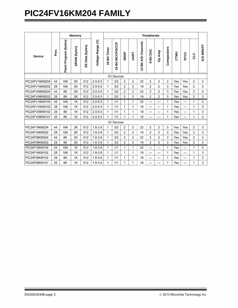
PIC24FV16KM204 FAMILY
Device Pin
s
Memory
Vo
lta
ge
Ra
ng
e (
V)
Peripherals
ICD
BR
KP
T
Fla
sh
Pro
gra
m (
by
tes
)
SR
AM
(b
yte
s)
EE
Da
ta (
by
tes
)
16
-Bit
Tim
er
16
-Bit
MC
CP
/SC
CP
MS
SP
UA
RT
12
-Bit
A/D
Ch
an
ne
ls
8-B
it D
AC
Op
Am
p
Co
mp
ara
tors
CT
MU
RT
CC
CL
C
5V Devices
PIC24FV16KM204 44 16K 2K 512 2.0-5.5 1 3/2 2 2 22 2 2 3 Yes Yes 2 3
PIC24FV16KM202 28 16K 2K 512 2.0-5.5 1 3/2 2 2 19 2 2 3 Yes Yes 2 3
PIC24FV08KM204 44 8K 2K 512 2.0-5.5 1 3/2 2 2 22 2 2 3 Yes Yes 2 3
PIC24FV08KM202 28 8K 2K 512 2.0-5.5 1 3/2 2 2 19 2 2 3 Yes Yes 2 3
PIC24FV16KM104 44 16K 1K 512 2.0-5.5 1 1/1 1 1 22 — — 1 Yes — 1 3
PIC24FV16KM102 28 16K 1K 512 2.0-5.5 1 1/1 1 1 19 — — 1 Yes — 1 3
PIC24FV08KM102 28 8K 1K 512 2.0-5.5 1 1/1 1 1 19 — — 1 Yes — 1 3
PIC24FV08KM101 20 8K 1K 512 2.0-5.5 1 1/1 1 1 16 — — 1 Yes — 1 3
3V Devices
PIC24F16KM204 44 16K 2K 512 1.8-3.6 1 3/2 2 2 22 2 2 3 Yes Yes 2 3
PIC24F16KM202 28 16K 2K 512 1.8-3.6 1 3/2 2 2 19 2 2 3 Yes Yes 2 3
PIC24F08KM204 44 8K 2K 512 1.8-3.6 1 3/2 2 2 22 2 2 3 Yes Yes 2 3
PIC24F08KM202 28 8K 2K 512 1.8-3.6 1 3/2 2 2 19 2 2 3 Yes Yes 2 3
PIC24F16KM104 44 16K 1K 512 1.8-3.6 1 1/1 1 1 22 — — 1 Yes — 1 3
PIC24F16KM102 28 16K 1K 512 1.8-3.6 1 1/1 1 1 19 — — 1 Yes — 1 3
PIC24F08KM102 28 8K 1K 512 1.8-3.6 1 1/1 1 1 19 — — 1 Yes — 1 3
PIC24F08KM101 20 8K 1K 512 1.8-3.6 1 1/1 1 1 16 — — 1 Yes — 1 3
DS30003030B-page 2 2013 Microchip Technology Inc.

PIC24FV16KM204 FAMILY
Peripheral Features
• High-Current Sink/Source, 18 mA/18 mA All Ports
• Independent Ultra Low-Power, 32 kHz Timer Oscillator
• Up to Two Master Synchronous Serial Ports (MSSPs) with SPI and I2C™ modes:
In SPI mode:
- User-configurable SCKx and SDOx pin outputs
- Daisy-chaining of SPI slave devices
In I2 C mode:
- Serial clock synchronization (clock stretching)
- Bus collision detection and will arbitrate accordingly
- Support for 16-bit read/write interface
• Up to Two Enhanced Addressable UARTs:
- LIN/J2602 bus support (auto-wake-up, Auto-Baud Detect, Break character support)
- High and low speed (SCI)
- IrDA® mode (hardware encoder/decoder function)
• Two External Interrupt Pins
• Hardware Real-Time Clock and Calendar (RTCC)
• Configurable Reference Clock Output (REFO)
• Two Configurable Logic Cells (CLC)
• Up to Two Single Output Capture/Compare/PWM (SCCP) modules and up to Three Multiple Output Capture/Compare/PWM (MCCP) modules
Special Microcontroller Features
• Wide Operating Voltage Range Options:
- 1.8V to 3.6V (PIC24F devices)
- 2.0V to 5.0V (PIC24FV devices)
• Selectable Power Management modes:
- Idle: CPU shuts down, allowing for significant power reduction
- Sleep: CPU and peripherals shut down for substantial power reduction and fast wake-up
- Retention Sleep mode: PIC24FV devices can enter Sleep mode, employing the Retention Regulator, further reducing power consumption
- Doze: CPU can run at a lower frequency than peripherals, a user-programmable feature
- Alternate Clock modes allow on-the-fly switching to a lower clock speed for selective power reduction
• Fail-Safe Clock Monitor:
- Detects clock failure and switches to on-chip, low-power RC Oscillator
• Ultra Low-Power Wake-up Pin Provides an External Trigger for Wake from Sleep
• 10,000 Erase/Write Cycle Endurance Flash Program Memory, Typical
• 100,000 Erase/Write Cycle Endurance Data EEPROM, Typical
• Flash and Data EEPROM Data Retention: 20 Years Minimum
• Self-Programmable under Software Control
• Power-on Reset (POR), Power-up Timer (PWRT) and Oscillator Start-up Timer (OST)
• Watchdog Timer (WDT) with its Own On-Chip RC Oscillator for Reliable Operation
• On-Chip Regulator for 5V Operation
• Selectable Windowed WDT Feature
• Selectable Oscillator Options including:
- 4x Phase Locked Loop (PLL)
• 8 MHz (FRC) Internal RC Oscillator:
- HS/EC, High-Speed Crystal/Resonator Oscillator or External Clock
• In-Circuit Serial Programming™ (ICSP™) and In-Circuit Emulation (ICE) – via Two Pins
• In-Circuit Debugging
• Programmable High/Low-Voltage Detect (HLVD) module
• Programmable Brown-out Reset (BOR):
- Software enable feature
- Configurable shutdown in Sleep
- Auto-configures power mode and sensitivity based on device operating speed
- LPBOR available for re-arming of the POR
2013 Microchip Technology Inc. DS30003030B-page 3

PIC24FV16KM204 FAMILY
Pin Diagrams
PinPin Features
PIC24F08KM101 PIC24FVKM08KM101
1 MCLR/VPP/RA5
2 PGEC2/CVREF+/VREF+/AN0/CN2/RA0
3 PGED2/CVREF-/VREF-/AN1/CN3/RA1
4 PGED1/AN2/CTCMP/ULPWU/C1IND/OC2A/CN4/RB0
5 PGEC1/AN3/C1INC/CTED12/CN5/RB1
6 AN4/U1RX/TCKIB/CTED13/CN6/RB2
7 OSCI/CLKI/AN13/C1INB/CN30/RA2
8 OSCO/CLKO/AN14/C1INA/CN29/RA3
9 PGED3/SOSCI/AN15/CLCINA/CN1/RB4
10 PGEC3/SOSCO/SCLKI/AN16/PWRLCLK/CLCINB/CN0/RA4
11 AN19/U1TX/CTED1/INT0/CN23/RB7 AN19/U1TX/IC1/OC1A/CTED1/INT0/CN23/RB7
12 AN20/SCL1/U1CTS/OC1B/CTED10/CN22/RB8
13 AN21/SDA1/T1CK/U1RTS/U1BCLK/IC2/CLC1O/CTED4/CN21/RB9
14 IC1/OC1A/INT2/CN8/RA6 VCAP OR VDDCORE
15 AN12/HLVDIN/SCK1/OC1C/CTED2/CN14/RB12 AN12/HLVDIN/SCK1/OC1C/CTED2/INT2/CN14/RB12
16 AN11/SDO1/OCFB/OC1D/CTPLS/CN13/RB13
17 CVREF/AN10/SDI1/C1OUT/OCFA/CTED5/INT1/CN12/RB14
18 AN9/REFO/SS1/TCKIA/CTED6/CN11/RB15
19 VSS/AVSS
20 VDD/AVDD
20-Pin PDIP/SSOP/SOIC
PIC
24
F0
8K
M1
01
RA5
RA3
RA0RA1
VDD
VSS
RB0
RB7RA4RB4 RB8
RA2RB2RB1
12345678910
20191817161514131211
RB15RB14RB13
RB9RA6 OR VDDCORERB12
DS30003030B-page 4 2013 Microchip Technology Inc.

PIC24FV16KM204 FAMILY
Pin Diagrams (Continued)
20-Pin QFN
PinPin Features
PIC24F08KM101 PIC24FV08KM101
1 PGED1/AN2/CTCMP/ULPWU/C1IND/OC2A/CN4/RB0
2 PGEC1/AN3/C1INC/CTED12/CN5/RB1
3 AN4/U1RX/TCKIB/CTED13/CN6/RB2
4 OSCI/CLKI/AN13/C1INB/CN30/RA2
5 OSCO/CLKO/AN14/C1INA/CN29/RA3
6 PGED3/SOSCI/AN15/CLCINA/CN1/RB4
7 PGEC3/SOSCO/SCLKI/AN16/PWRLCLK/CLCINB/CN0/RA4
8 AN19/U1TX/CTED1/INT0/CN23/RB7 AN19/U1TX/IC1/OC1A/CTED1/INT0/CN23/RB7
9 AN20/SCL1/U1CTS/OC1B/CTED10/CN22/RB8
10 AN21/SDA1/T1CK/U1RTS/U1BCLK/IC2/CLC1O/CTED4/CN21/RB9
11 IC1/OC1A/INT2/CN8/RA6 VCAP OR VDDCORE
12 AN12/HLVDIN/SCK1/OC1C/CTED2/CN14/RB12 AN12/HLVDIN/SCK1/OC1C/CTED2/INT2/CN14/RB12
13 AN11/SDO1/OCFB/OC1D/CTPLS/CN13/RB13
14 CVREF/AN10/SDI1/C1OUT/OCFA/CTED5/INT1/CN12/RB14
15 AN9/REFO/SS1/TCKIA/CTED6/CN11/RB15
16 VSS/AVSS
17 VDD/AVDD
18 MCLR/VPP/RA5
19 PGEC2/CVREF+ /VREF+/AN0/CN2/RA0
20 PGED2/CVREF-/VREF-/AN1/CN3/RA1
PIC24F08KM101
2
3
1
5
4
6 7 8 9 1011
12
13
14
151617181920
RB0
RB1
RB2
RA2
RA3
RB
7
RB
9
RA
4
RB
4
RB
8
RA6 or VDDCORE
RB12
RB13
RB14
RB15
CV
RE
F-
CV
RE
F+
RA
5
RA
0
RA
1
2013 Microchip Technology Inc. DS30003030B-page 5

PIC24FV16KM204 FAMILY
Pin Diagrams (Continued)
PinPin Features
PIC24FXXKMX02 PIC24FVXXKMX02
1 MCLR/VPP/RA5
2 CVREF+/VREF+/DAC1REF+/AN0/C3INC/CN2/RA0
3 CVREF-/VREF-/AN1/CN3/RA1 CVREF-/VREF-/AN1/RA1
4 PGED1/AN2/CTCMP/ULPWU/C1IND/C2INB/C3IND/U2TX/CN4/RB0
5 PGEC1/OA1INA/OA2INA/AN3/C1INC/C2INA/U2RX/CTED12/CN5/RB1
6 OA1INB/OA2INB/AN4/C1INB/C2IND/SDA2/U1RX/TCKIB/CTED13/CN6/RB2
7 OA1OUT/AN5/C1INA/C2INC/SCL2/CN7/RB3
8 VSS
9 OSCI/CLKI/AN13/CN30/RA2
10 OSCO/CLKO/AN14/CN29/RA3
11 SOSCI/AN15/U2RTS/U2BCLK/CN1/RB4
12 SOSCO/SCLKI/AN16/PWRLCLK/U2CTS/CN0/RA4
13 VDD
14 PGED3/AN17/ASDA1/SCK2/IC4/OC1E/CLCINA/CN27/RB5
15 PGEC3/AN18/ASCL1/SDO2/IC5/OC1F/CLCINB/CN24/RB6
16 AN19/U1TX/INT0/CN23/RB7 AN19/U1TX/C2OUT/OC1A/INT0/CN23/RB7
17 AN20/SCL1/U1CTS/C3OUT/OC1B/CTED10/CN22/RB8
18 AN21/SDA1/T1CK/U1RTS/U1BCLK/IC2/OC4/CLC1O/CTED4/CN21/RB9
19 SDI2/IC1/OC5/CLC2O/CTED3/CN9/RA7
20 C2OUT/OC1A/CTED1/INT2/CN8/RA6 VCAP OR VDDCORE
21 PGED2/SDI1/OC3A/OC1C/CTED11/CN16/RB10
22 PGEC2/SCK1/OC2A/CTED9/CN15/RB11
23 DAC1OUT/AN12/HLVDIN/SS2/IC3/OC2B/CTED2/CN14/RB12 DAC1OUT/AN12/HLVDIN/SS2/IC3/OC2B/CTED2/INT2/CN14/RB12
24 OA1INC/OA2INC/AN11/SDO1/OCFB/OC3B/OC1D/CTPLS/CN13/RB13
25 DAC2OUT/CVREF/OA1IND/OA2IND/AN10/C3INB/RTCC/C1OUT/OCFA/CTED5/INT1/CN12/RB14
26 DAC2REF+/OA2OUT/AN9/C3INA/REFO/SS1/TCKIA/CTED6/CN11/RB15
27 VSS/AVSS
28 VDD/AVDD
28-Pin SPDIP/SSOP/SOIC
PIC
24
F1
6K
MX
02
MCLR/RA5
VSS
RA0RA1
AVDD
AVSS
RB0
RA7RA3RA2 RA6 or VDDCORE
RB3RB2RB1
12345678910
28272625242322212019
RB15RB14RB13
RB10RB11RB12
RA4
RB6RB5VDD RB7
11121314
18171615
RB8RB9RB4
Legend: Values in red indicate pin function differences between PIC24F(V)XXKM202 and PIC24F(V)XXKM102 devices.
DS30003030B-page 6 2013 Microchip Technology Inc.

PIC24FV16KM204 FAMILY
Pin Diagrams (Continued)
Legend: Values in red indicate pin function differences between PIC24F(V)XXKM202 and PIC24F(V)XXKM102 devices.
Note 1: Exposed pad on underside of device is connected to VSS.
28-Pin QFN(1)
10 11
23
6
1
18192021
22
12 13 1415
87
1617
232425262728
9
PIC24F16KMX02
54
MC
LR/R
A5
VSS
VD
DR
A0
RA
1
VD
D
VS
S
RB0
RB
6
RA
4R
B4
RA7RA3RA2
RA6 OR VDDCORE
RB
7
RB9
RB
8
RB3RB2RB1
RB
15
RB
14
RB13RB12
RB10RB11
RB
5
PinPin Features Pin Features
PIC24FXXKMX02 PIC24FVXXKMX02
1 PGED1/AN2/CTCMP/ULPWU/C1IND/C2INB/C3IND/U2TX/CN4/RB0
2 PGEC1/OA1INA/OA2INA/AN3/C1INC/C2INA/U2RX/CTED12/CN5/RB1
3 OA1INB/OA2INB/AN4/C1INB/C2IND/SDA2/U1RX/TCKIB/CTED13/CN6/RB2
4 OA1OUT/AN5/C1INA/C2INC/SCL2/CN7/RB3
5 VSS
6 OSCI/CLKI/AN13/CN30/RA2
7 OSCO/CLKO/AN14/CN29/RA3
8 SOSCI/AN15/U2RTS/U2BCLK/CN1/RB4
9 SOSCO/SCLKI/AN16/PWRLCLK/U2CTS/CN0/RA4
10 VDD
11 PGED3/AN17/ASDA1/SCK2/IC4/OC1E/CLCINA/CN27/RB5
12 PGEC3/AN18/ASCL1/SDO2/IC5/OC1F/CLCINB/CN24/RB6
13 AN19/U1TX/INT0/CN23/RB7 AN19/U1TX/C2OUT/OC1A/INT0/CN23/RB7
14 AN20/SCL1/U1CTS/C3OUT/OC1B/CTED10/CN22/RB8
15 AN21/SDA1/T1CK/U1RTS/U1BCLK/IC2/OC4/CLC1O/CTED4/CN21/RB9
16 SDI2/IC1/OC5/CLC2O/CTED3/CN9/RA7
17 C2OUT/OC1A/CTED1/INT2/CN8/RA6 VDDCORE/VCAP
18 PGED2/SDI1/OC3A/OC1C/CTED11/CN16/RB10
19 PGEC2/SCK1/OC2A/CTED9/CN15/RB11
20 DAC1OUT/AN12/HLVDIN/SS2/IC3/OC2B/CTED2/CN14/RB12 DAC1OUT/AN12/HLVDIN/SS2/IC3/OC2B/CTED2/INT2/CN14/RB12
21 OA1INC/OA2INC/AN11/SDO1/OCFB/OC3B/OC1D/CTPLS/CN13/RB13
22 DAC2OUT/CVREF/OA1IND/OA2IND/AN10/C3INB/RTCC/C1OUT/OCFA/CTED5/INT1/CN12/RB14
23 DAC2REF+/OA2OUT/AN9/C3INA/REFO/SS1/TCKIA/CTED6/CN11/RB15
24 VSS
25 VDD
26 MCLR/VPP/RA5
27 CVREF+/VREF+/DAC1REF+/AN0/C3INC/CN2/RA0 CVREF+/VREF+/DAC1REF+/AN0/C3INC/CTED1/CN2/RA0
28 CVREF-/VREF-/AN1/CN3/RA1
2013 Microchip Technology Inc. DS30003030B-page 7

PIC24FV16KM204 FAMILY
Pin Diagrams (Continued)
Legend: Values in red indicate pin function differences between PIC24F(V)XXKM202 and PIC24F(V)XXKM102 devices.
Note 1: Exposed pad on underside of device is connected to VSS.
PinPin Features
PIC24FXXKMX04 PIC24FVXXKMX04
1 AN21/SDA1/T1CK/U1RTS/U1BCLK/IC2/OC4/CLC1O/CTED4/CN21/RB9
2 U1RX/OC2C/CN18/RC6
3 U1TX/OC2D/CN17/RC7
4 OC2E/CN20/RC8
5 IC4/OC2F/CTED7/CN19/RC9
6 IC1/OC5/CLC2O/CTED3/CN9/RA7
7 C2OUT/OC1A/CTED1/INT2/CN8/RA6 VCAP or VDDCORE
8 PGED2/SDI1/OC1C/CTED11/CN16/RB10
9 PGEC2/SCK1/OC2A/CTED9/CN15/RB11
10 DAC1OUT/AN12/HLVDIN/OC2B/CTED2/CN14/RB12
DAC1OUT/AN12/HLVDIN/OC2B/CTED2/INT2/CN14/RB12
11 OA1INC/OA2INC/AN11/SDO1/OC1D/CTPLS/CN13/RB13
12 IC5/OC3A/CN35/RA10
13 IC3/OC3B/CTED8/CN36/RA11
14 DAC2OUT/CVREF/OA1IND/OA2IND/AN10/C3INB/RTCC/C1OUT/OCFA/CTED5/INT1/CN12/RB14
15 DAC2REF+/OA2OUT/AN9/C3INA/REFO/SS1/TCKIA/CTED6/CN11/RB15
16 AVSS
17 AVDD
18 MCLR/VPP/RA5
19 CVREF+/VREF+/DAC1REF+/AN0/C3INC/CN2/RA0
CVREF+/VREF+/DAC1REF+/AN0/C3INC/CTED1/CN2/RA0
20 CVREF-/VREF-/AN1/CN3/RA1
21 PGED1/AN2/CTCMP/ULPWU/C1IND/C2INB/C3IND/U2TX/CN4/RB0
22 PGEC1/OA1INA/OA2INA/AN3/C1INC/C2INA/U2RX/CTED12/CN5//RB1
23 OA1INB/OA2INB/AN4/C1INB/C2IND/SDA2/TCKIB/CTED13/CN6/RB2
24 OA1OUT/AN5/C1INA/C2INC/SCL2/CN7/RB3
25 AN6/CN32/RC0
26 AN7/CN31/RC1
27 AN8/CN10/RC2
28 VDD
29 VSS
30 OSCI/CLKI/AN13/CN30/RA2
31 OSCO/CLKO/AN14/CN29/RA3
32 OCFB/CN33/RA8
33 SOSCI/AN15/U2RTS/U2BCLK/CN1/RB4
34 SOSCO/SCLKI/AN16/PWRLCLK/U2CTS/CN0/RA4
35 SS2/CN34/RA9
36 SDI2/CN28/RC3
37 SDO2/CN25/RC4
38 SCK2/CN26/RC5
39 VSS
40 VDD
41 PGED3/AN17/ASDA1/OC1E/CLCINA/CN27/RB5
42 PGEC3/AN18/ASCL1/OC1F/CLCINB/CN24/RB6
43 AN19/INT0/CN23/RB7 AN19/C2OUT/OC1A/INT0/CN23/RB7
44 AN20/SCL1/U1CTS/C3OUT/OC1B/CTED10/CN22/RB8
1011
23456
1
18 19 20 21 2212 13 14 15
38
87
44
43
42
41
40
39
16 17
2930313233
232425262728
36
34
35
9
PIC24FXXKMX04
37
RB
8R
B7
RB
6R
B5
VD
D
VS
S
RC
5R
C4
RC
3R
A9
RA
4
RB4RA8RA3RA2VSS
VDD
RC2RC1RC0RB3RB2
RB9RC6RC7RC8RC9RA7RA6RB10RB11RB12RB13
RB
1R
B0
RA
1R
A0
MC
LR
/RA
5A
VD
D
AV
SS
RB
15
RB
14R
A11
RA
1044-Pin TQFP/QFN(1)
DS30003030B-page 8 2013 Microchip Technology Inc.

PIC24FV16KM204 FAMILY
Pin Diagrams (Continued)
PinPin Features
PIC24FXXKMX04 PIC24FVXXKMX04
1 AN21/SDA1/T1CK/U1RTS/U1BCLK/IC2/OC4/CLC1O/CTED4/CN21/RB9
2 U1RX/OC2C/CN18/RC6
3 U1TX/OC2D/CN17/RC7
4 OC2/CN20/RC8
5 IC4/OC2F/CTED7/CN19/RC9
6 IC1/OC5/CLC2O/CTED3/CN9/RA7
7 C2OUT/OC1A/CTED1/INT2/CN8/RA6 VDDCORE or VCAP
8 n/c n/c
9 PGED2/SDI1/OC1C/CTED11/CN16/RB10
10 PGEC2/SCK1/OC2A/CTED9/CN15/RB11
11 DAC1OUT/AN12/HLVDIN/OC2B/CTED2/CN14/RB12
DAC1OUT/AN12/HLVDIN/OC2B/CTED2/INT2/CN14/RB12
12 OA1INC/OA2INC/AN11/SDO1/OC1D/CTPLS/CN13/RB13
13 IC5/OC3A/CN35/RA10
14 IC3/OC3B/CTED8/CN36/RA11
15 DAC2OUT/CVREF/OA1IND/OA2IND/AN10/C3INB/RTCC/C1OUT/OCFA/CTED5/INT1/CN12/RB14
16 DAC2REF+/OA2OUT/AN9/C3INA/REFO/SS1/TCKIA/CTED6/CN11/RB15
17 VSS/AVSS
18 VDD/AVDD
19 MCLR/VPP/RA5
20 n/c
21 CVREF+/VREF+/DAC1REF+/AN0/C3INC/CN2/RA0
CVREF+/VREF+/DAC1REF+/AN0/C3INC/CTED1/CN2/RA0
22 CVREF-/VREF-/AN1/CN3/RA1
23 PGED1/AN2/CTCMP/ULPWU/C1IND/C2INB/C3IND/U2TX/CN4/RB0
24 PGEC1/OA1INA/OA2INA/AN3/C1INC/C2INA/U2RX/CTED12/CN5/RB1
25 OA1INB/OA2INB/AN4/C1INB/C2IND/SDA2/TCKIB/CTED13/CN6/RB2
26 OA1OUT/AN5/C1INA/C2INC/SCL2/CN7/RB3
27 AN6/CN32/RC0
28 AN7/CN31/RC1
29 AN8/CN10/RC2
30 VDD
31 VSS
32 n/c
33 OSCI/AN13/CLKI/CN30/RA2
34 OSCO/CLKO/AN14/CN29/RA3
35 OCFB/CN33/RA8
36 SOSCI/AN15/U2RTS/U2BCLK/CN1/RB4
37 SOSCO/SCLKI/AN16/PWRLCLK/U2CTS/CN0/RA4
38 SS2/CN34/RA9
39 SDI2/CN28/RC3
40 SDO2/CN25/RC4
41 SCK2/CN26/RC5
42 VSS
43 VDD
44 n/c
45 PGED3/AN17/ASDA1/OC1E/CLCINA/CN27/RB5
46 PGEC3/AN18/ASCL1/OC1F/CLCINB/CN24/RB6
47 AN19/INT0/CN23/RB7 AN19/C2OUT/OC1A/INT0/CN23/RB7
48 AN20/SCL1/U1CTS/C3OUT/OC1B/CTED10/CN22/RB8
48-Pin UQFN(1)
RB
8R
B7
RB
6R
B5
n/c
VD
D
VS
S
RC
5R
C4
RC
3R
A9
RA
4
48 47 46 45 44 43 42 41
40 39 38 37RB9 1 36 RB4RC6 2 35 RA8RC7 3 34 RA3RC8 4 33 RA2RC9 5 32 n/cRA7 6 PIC24FXXKMX04 31 VSSRA6 7 30 VDD
n/c 8 29 RC2RB10 9 28 RC1RB11 10 27 RC0RB12 11 26 RB3RB13 12 25 RB2
13 14 15 16 17 18 19 20 21 22 23 24
RA
10R
A11
RB
14R
B15
VS
S/A
VS
S
VD
D/A
VD
D
n/c
RA
0R
A1
RB
0R
B1
PIC24FVXXKMX04
MC
LR/R
A5
Legend: Values in red indicate pin function differences between PIC24F(V)XXKM202 and PIC24F(V)XXKM102 devices.
Note 1: Exposed pad on underside of device is connected to VSS.
2013 Microchip Technology Inc. DS30003030B-page 9

PIC24FV16KM204 FAMILY
Table of Contents
1.0 Device Overview ........................................................................................................................................................................ 132.0 Guidelines for Getting Started with 16-Bit Microcontrollers ........................................................................................................ 293.0 CPU ........................................................................................................................................................................................... 354.0 Memory Organization ................................................................................................................................................................. 415.0 Flash Program Memory.............................................................................................................................................................. 676.0 Data EEPROM Memory ............................................................................................................................................................. 737.0 Resets ........................................................................................................................................................................................ 798.0 Interrupt Controller ..................................................................................................................................................................... 859.0 Oscillator Configuration ............................................................................................................................................................ 12110.0 Power-Saving Features............................................................................................................................................................ 13111.0 I/O Ports ................................................................................................................................................................................... 13712.0 Timer1 ..................................................................................................................................................................................... 14113.0 Capture/Compare/PWM/Timer Modules (MCCP and SCCP) .................................................................................................. 14314.0 Master Synchronous Serial Port (MSSP) ................................................................................................................................. 15915.0 Universal Asynchronous Receiver Transmitter (UART) ........................................................................................................... 17316.0 Real-Time Clock and Calendar (RTCC) .................................................................................................................................. 18117.0 Configurable Logic Cell (CLC).................................................................................................................................................. 19518.0 High/Low-Voltage Detect (HLVD)............................................................................................................................................. 20719.0 12-Bit A/D Converter with Threshold Detect ............................................................................................................................ 20920.0 8-Bit Digital-to-Analog Converter (DAC)................................................................................................................................... 22921.0 Dual Operational Amplifier Module........................................................................................................................................... 23322.0 Comparator Module.................................................................................................................................................................. 23523.0 Comparator Voltage Reference................................................................................................................................................ 23924.0 Charge Time Measurement Unit (CTMU) ................................................................................................................................ 24125.0 Special Features ...................................................................................................................................................................... 24926.0 Development Support............................................................................................................................................................... 26127.0 Electrical Characteristics .......................................................................................................................................................... 26528.0 Packaging Information.............................................................................................................................................................. 297Appendix A: Revision History............................................................................................................................................................. 325Index ................................................................................................................................................................................................. 327The Microchip Web Site ..................................................................................................................................................................... 333Customer Change Notification Service .............................................................................................................................................. 333Customer Support .............................................................................................................................................................................. 333Product Identification System............................................................................................................................................................. 335
DS30003030B-page 10 2013 Microchip Technology Inc.
PIC24FV16KM204 FAMILY
TO OUR VALUED CUSTOMERS
It is our intention to provide our valued customers with the best documentation possible to ensure successful use of your Microchipproducts. To this end, we will continue to improve our publications to better suit your needs. Our publications will be refined andenhanced as new volumes and updates are introduced.
If you have any questions or comments regarding this publication, please contact the Marketing Communications Department viaE-mail at [email protected]. We welcome your feedback.
Most Current Data Sheet
To obtain the most up-to-date version of this data sheet, please register at our Worldwide Web site at:
http://www.microchip.com
You can determine the version of a data sheet by examining its literature number found on the bottom outside corner of any page.The last character of the literature number is the version number, (e.g., DS30000000A is version A of document DS30000000).
Errata
An errata sheet, describing minor operational differences from the data sheet and recommended workarounds, may exist for currentdevices. As device/documentation issues become known to us, we will publish an errata sheet. The errata will specify the revisionof silicon and revision of document to which it applies.
To determine if an errata sheet exists for a particular device, please check with one of the following:
• Microchip’s Worldwide Web site; http://www.microchip.com• Your local Microchip sales office (see last page)When contacting a sales office, please specify which device, revision of silicon and data sheet (include literature number) you areusing.
Customer Notification System
Register on our web site at www.microchip.com to receive the most current information on all of our products.
2013 Microchip Technology Inc. DS30003030B-page 11

PIC24FV16KM204 FAMILY
NOTES:
DS30003030B-page 12 2013 Microchip Technology Inc.

PIC24FV16KM204 FAMILY
1.0 DEVICE OVERVIEW
This document contains device-specific information forthe following devices:
The PIC24FV16KM204 family introduces many newanalog features to the extreme low-power Microchipdevices. This is a 16-bit microcontroller family with abroad peripheral feature set and enhanced computa-tional performance. This family also offers a newmigration option for those high-performance applica-tions which may be outgrowing their 8-bit platforms, butdo not require the numerical processing power of aDigital Signal Processor (DSC).
1.1 Core Features
1.1.1 16-BIT ARCHITECTURE
Central to all PIC24F devices is the 16-bit modifiedHarvard architecture, first introduced with Microchip’sdsPIC® Digital Signal Controllers. The PIC24F CPUcore offers a wide range of enhancements, such as:
• 16-bit data and 24-bit address paths with the ability to move information between data and memory spaces
• Linear Addressing of up to 16 Mbytes (program space) and 16 Kbytes (data)
• A 16-element working register array with built-in software stack support
• A 17 x 17 hardware multiplier with support for integer math
• Hardware support for 32-bit by 16-bit division
• An instruction set that supports multiple address-ing modes and is optimized for high-level languages, such as C
• Operational performance up to 16 MIPS
1.1.2 POWER-SAVING TECHNOLOGY
All of the devices in the PIC24FV16KM204 family incor-porate a range of features that can significantly reducepower consumption during operation. Key featuresinclude:
• On-the-Fly Clock Switching, to allow the device clock to be changed under software control to the Timer1 source or the internal, low-power RC Oscillator during operation, allowing users to incorporate power-saving ideas into their software designs.
• Doze Mode Operation, when timing-sensitive applications, such as serial communications, require the uninterrupted operation of peripherals, the CPU clock speed can be selectively reduced, allowing incremental power savings without missing a beat.
• Instruction-Based Power-Saving Modes, to allow the microcontroller to suspend all operations or selectively shut down its core while leaving its peripherals active with a single instruction in software.
1.1.3 OSCILLATOR OPTIONS AND FEATURES
The PIC24FV16KM204 family offers five different oscil-lator options, allowing users a range of choices indeveloping application hardware. These include:
• Two Crystal modes using crystals or ceramic resonators.
• Two External Clock (EC) modes offering the option of a divide-by-2 clock output.
• Two Fast Internal Oscillators (FRCs), one with a nominal 8 MHz output and the other with a nominal 500 kHz output. These outputs can also be divided under software control to provide clock speed as low as 31 kHz or 2 kHz.
• A Phase Locked Loop (PLL) frequency multiplier, available to the external oscillator modes and the 8 MHz FRC Oscillator, which allows clock speeds of up to 32 MHz.
• A separate internal RC Oscillator (LPRC) with a fixed 31 kHz output, which provides a low-power option for timing-insensitive applications.
The internal oscillator block also provides a stable ref-erence source for the Fail-Safe Clock Monitor (FSCM).This option constantly monitors the main clock sourceagainst a reference signal provided by the internaloscillator and enables the controller to switch to theinternal oscillator, allowing for continued low-speedoperation or a safe application shutdown.
• PIC24FV08KM101 • PIC24F08KM101
• PIC24FV08KM102 • PIC24F08KM102
• PIC24FV16KM102 • PIC24F16KM102
• PIC24FV16KM104 • PIC24F16KM104
• PIC24FV08KM202 • PIC24F08KM202
• PIC24FV08KM204 • PIC24F08KM204
• PIC24FV16KM202 • PIC24F16KM202
• PIC24FV16KM204 • PIC24F16KM204
2013 Microchip Technology Inc. DS30003030B-page 13
PIC24FV16KM204 FAMILY
1.1.4 EASY MIGRATION
The PIC24FV16KM204 family devices have twovariants. The KM20X variant provides the full feature setof the device, while the KM10X offers a reduced periph-eral set, allowing for the balance of features and cost(refer to Table 1-1). Both variants allow for a smoothmigration path as applications grow and evolve.
The consistent pinout scheme used throughout the entirefamily also helps in migrating to the next larger device.This is true when moving between devices with the samepin count, different die variants, or even moving from20-pin or 28-pin devices to 44-pin/48-pin devices.
The PIC24F family is pin compatible with devices in thedsPIC33 family, and shares some compatibility with thepinout schema for PIC18 and dsPIC30. This extendsthe ability of applications to grow from the relativelysimple to the powerful and complex, yet still selecting aMicrochip device.
1.2 Other Special Features
• Communications: The PIC24FV16KM204 family incorporates a range of serial communication peripherals to handle a range of application requirements. There is an MSSP module which implements both SPI and I2C™ protocols, and supports both Master and Slave modes of operation for each. Devices also include one of two UARTs with built-in IrDA® encoders/decoders.
• Analog Features: Select members of the PIC24FV16KM204 family include two 8-bit Digital-to-Analog Converters which offer support in Idle mode, and left and right justified input data, as well as up to two operational amplifiers with selectable power and speed modes.
• Real-Time Clock/Calendar (RTCC): This module implements a full-featured clock and calendar with alarm functions in hardware, freeing up timer resources and program memory space for use of the core application.
• 12-Bit A/D Converter: This module incorporates programmable acquisition time, allowing for a channel to be selected and a conversion to be initiated without waiting for a sampling period, and faster sampling speed. The 16-deep result buffer can be used either in Sleep, to reduce power, or in Active mode to improve throughput.
• Charge Time Measurement Unit (CTMU) Interface: The PIC24FV16KM204 family includes the new CTMU interface module, which can be used for capacitive touch sensing, proximity sensing, and also for precision time measurement and pulse generation. The CTMU can also be connected to the operational amplifiers to provide active guard-ing, which provides increased robustness in the presence of noise in capacitive touch applications.
1.3 Details on Individual Family Members
Devices in the PIC24FV16KM204 family are availablein 20-pin, 28-pin, 44-pin and 48-pin packages. Thegeneral block diagram for all devices is shown inFigure 1-1.
Members of the PIC24FV16KM204 family are availableas both standard and high-voltage devices. High-voltagedevices, designated with an “FV” in the part number(such as PIC24FV16KM204), accommodate an operat-ing VDD range of 2.0V to 5.5V and have an on-boardvoltage regulator that powers the core. Peripheralsoperate at VDD.
Standard devices, designated by “F” (such asPIC24F16KM204), function over a lower VDD range of1.8V to 3.6V. These parts do not have an internal regu-lator, and both the core and peripherals operate directlyfrom VDD.
The PIC24FV16KM204 family may be thought of astwo different device groups, both offering slightly differ-ent sets of features. These differ from each other inmultiple ways:
• The size of the Flash program memory
• The number of external analog channels available
• The number of Digital-to-Analog Converters
• The number of operational amplifiers
• The number of analog comparators
• The presence of a Real-Time Clock and Calendar (RTCC)
• The number and type of CCP modules (i.e., MCCP vs. SCCP)
• The number of serial communication modules (both MSSPs and UARTs)
• The number of Configurable Logic Cell (CLC) modules
The general differences between the differentsub-families are shown in Table 1-1 and Table 1-2.
A list of the pin features available on thePIC24FV16KM204 family devices, sorted by function,is provided in Table 1-5.
DS30003030B-page 14 2013 Microchip Technology Inc.

PIC24FV16KM204 FAMILY
TABLE 1-1: DEVICE FEATURES FOR THE PIC24F16KM204 FAMILY
Features
PIC
24F
16K
M20
4
PIC
24F
08K
M20
4
PIC
24F
16K
M20
2
PIC
24F
08K
M20
2
Operating Frequency DC-32 MHz
Program Memory (bytes) 16K 8K 16K 8K
Program Memory (instructions) 5632 2816 5632 2816
Data Memory (bytes) 2048
Data EEPROM Memory (bytes) 512
Interrupt Sources (soft vectors/NMI traps) 40 (36/4)
Voltage Range 1.8-3.6V
I/O Ports PORTA<11:0>PORTB<15:0>PORTC<9:0>
PORTA<7:0>PORTB<15:0>
Total I/O Pins 38 24
Timers 11 (One 16-bit timer, five MCCPs/SCCPs with up to two 16/32 timers each)
Capture/Compare/PWM modulesMCCPSCCP
32
Serial CommunicationsMSSPUART
22
Input Change Notification Interrupt 37 23
12-Bit Analog-to-Digital Module(input channels)
22 22 19 19
Analog Comparators 3
8-Bit Digital-to-Analog Converters 2
Operational Amplifiers 2
Charge Time Measurement Unit (CTMU) Yes
Real-Time Clock and Calendar (RTCC) Yes
Configurable Logic Cell (CLC) 2
Resets (and delays) POR, BOR, RESET Instruction, MCLR, WDT, Illegal Opcode,REPEAT Instruction, Hardware Traps, Configuration Word Mismatch
(PWRT, OST, PLL Lock)
Instruction Set 76 Base Instructions, Multiple Addressing Mode Variations
Packages 44-Pin QFN/TQFP,48-Pin UQFN
28-PinSPDIP/SSOP/SOIC/QFN
2013 Microchip Technology Inc. DS30003030B-page 15

PIC24FV16KM204 FAMILY
TABLE 1-2: DEVICE FEATURES FOR THE PIC24F16KM104 FAMILY
Features
PIC
24F
16K
M10
4
PIC
24F
16K
M10
2
PIC
24F
08K
M10
2
PIC
24F
08K
M10
1
Operating Frequency DC-32 MHz
Program Memory (bytes) 16K 16K 8K 8K
Program Memory (instructions) 5632 5632 2816 2816
Data Memory (bytes) 1024
Data EEPROM Memory (bytes) 512
Interrupt Sources (soft vectors/NMI traps) 25 (21/4)
Voltage Range 1.8-3.6V
I/O Ports PORTA<11:0>PORTB<15:0>PORTC<9:0>
PORTA<7:0>PORTB<15:0>
PORTA<6:0>PORTB<15:12,9:7,
4,2:0>
Total I/O Pins 38 24 18
Timers 5 (One 16-bit timer, two MCCPs/SCCPs with up to two 16/32 timers each)
Capture/Compare/PWM modulesMCCPSCCP
11
Serial CommunicationsMSSPUART
11
Input Change Notification Interrupt 37 23 17
12-Bit Analog-to-Digital Module(input channels)
22 19 16
Analog Comparators 1
8-Bit Digital-to-Analog Converters —
Operational Amplifiers —
Charge Time Measurement Unit (CTMU) Yes
Real-Time Clock and Calendar (RTCC) —
Configurable Logic Cell (CLC) 1
Resets (and delays) POR, BOR, RESET Instruction, MCLR, WDT, Illegal Opcode,REPEAT Instruction, Hardware Traps, Configuration Word Mismatch
(PWRT, OST, PLL Lock)
Instruction Set 76 Base Instructions, Multiple Addressing Mode Variations
Packages 44-Pin QFN/TQFP,
48-Pin UQFN
28-PinSPDIP/SSOP/SOIC/QFN
20-Pin SOIC/SSOP/PDIP
DS30003030B-page 16 2013 Microchip Technology Inc.

PIC24FV16KM204 FAMILY
TABLE 1-3: DEVICE FEATURES FOR THE PIC24FV16KM204 FAMILY
Features
PIC
24F
V16
KM
204
PIC
24F
V08
KM
204
PIC
24F
V16
KM
202
PIC
24F
V08
KM
202
Operating Frequency DC-32 MHz
Program Memory (bytes) 16K 8K 16K 8K
Program Memory (instructions) 5632 2816 5632 2816
Data Memory (bytes) 2048
Data EEPROM Memory (bytes) 512
Interrupt Sources (soft vectors/NMI traps) 40 (36/4)
Voltage Range 2.0-5.5V
I/O Ports PORTA<11:7,5:0>PORTB<15:0>PORTC<9:0>
PORTA<7,5:0>PORTB<15:0>
Total I/O Pins 37 23
Timers 11 (One 16-bit timer, five MCCPs/SCCPs with up to two 16/32 timers each)
Capture/Compare/PWM modulesMCCPSCCP
32
Serial CommunicationsMSSPUART
22
Input Change Notification Interrupt 36 22
12-Bit Analog-to-Digital Module(input channels)
22 19
Analog Comparators 3
8-Bit Digital-to-Analog Converters 2
Operational Amplifiers 2
Charge Time Measurement Unit (CTMU) Yes
Real-Time Clock and Calendar (RTCC) Yes
Configurable Logic Cell (CLC) 2
Resets (and delays) POR, BOR, RESET Instruction, MCLR, WDT, Illegal Opcode,REPEAT Instruction, Hardware Traps, Configuration Word Mismatch
(PWRT, OST, PLL Lock)
Instruction Set 76 Base Instructions, Multiple Addressing Mode Variations
Packages 44-Pin QFN/TQFP,48-Pin UQFN
28-PinSPDIP/SSOP/SOIC/QFN
2013 Microchip Technology Inc. DS30003030B-page 17

PIC24FV16KM204 FAMILY
TABLE 1-4: DEVICE FEATURES FOR THE PIC24FV16KM104 FAMILY
Features
PIC
24F
V16
KM
104
PIC
24F
V16
KM
102
PIC
24F
V08
KM
102
PIC
24F
V08
KM
101
Operating Frequency DC-32 MHz
Program Memory (bytes) 16K 16K 8K 8K
Program Memory (instructions) 5632 5632 2816 2816
Data Memory (bytes) 1024
Data EEPROM Memory (bytes) 512
Interrupt Sources (soft vectors/NMI traps) 25 (21/4)
Voltage Range 2.0-5.5V
I/O Ports PORTA<11:7,5:0>PORTB<15:0>PORTC<9:0>
PORTA<7,5:0>PORTB<15:0>
PORTA<5:0>PORTB<15:12,9:7,
4,2:0>
Total I/O Pins 37 23 17
Timers 5 (One 16-bit timer, two MCCPs/SCCPs with up to two 16/32 timers each)
Capture/Compare/PWM modulesMCCPSCCP
11
Serial CommunicationsMSSPUART
11
Input Change Notification Interrupt 36 22 16
12-Bit Analog-to-Digital Module(input channels)
22 19 16
Analog Comparators 1
8-Bit Digital-to-Analog Converters —
Operational Amplifiers —
Charge Time Measurement Unit (CTMU) Yes
Real-Time Clock and Calendar (RTCC) —
Configurable Logic Cell (CLC) 1
Resets (and delays) POR, BOR, RESET Instruction, MCLR, WDT, Illegal Opcode,REPEAT Instruction, Hardware Traps, Configuration Word Mismatch
(PWRT, OST, PLL Lock)
Instruction Set 76 Base Instructions, Multiple Addressing Mode Variations
Packages 44-Pin QFN/TQFP,
48-Pin UQFN
28-PinSPDIP/SSOP/SOIC/QFN
20-Pin SOIC/SSOP/PDIP
DS30003030B-page 18 2013 Microchip Technology Inc.

PIC24FV16KM204 FAMILY
FIGURE 1-1: PIC24FXXXXX FAMILY GENERAL BLOCK DIAGRAMS
InstructionDecode and
Control
16
PCH
16
Program Counter
23
24
Data Bus
16
DivideSupport
16
16
16
8
InterruptController
PSV and TableData AccessControl Block
RepeatControlLogic
Data Latch
Data RAM
AddressLatch
Address Latch
Program Memory
Data Latch
16
Address Bus
Lite
ral D
ata
23
Control Signals
16
16
16 x 16W Reg Array
Multiplier17x17
PORTA(1)
RA<0:7>
PORTB(1)
RB<0:15>
Note 1: All pins or features are not implemented on all device pinout configurations. See Table 1-5 for I/O port pin descriptions.
ComparatorsMCCP1-3 CTMU
Op Amp
A/D12-Bit
DAC1/2 MSSP1/2 CLC1/2CN1-36(1) UART1/2
Data EEPROM
OSCI/CLKIOSCO/CLKO
VDD, VSS
TimingGeneration
MCLR
Power-upTimer
OscillatorStart-up Timer
Power-onReset
WatchdogTimer
BOR
FRC/LPRCOscillators
DSWDT
Timer1RTCC
REFO
HLVD
PORTC(1)
RC<9:0>
Precision
ReferenceBand Gap
Voltage
VCAP
Regulator
SCCP4/5
(I2C™, SPI)1/2
PCL
StackControlLogic
Read AGUWrite AGU
EA MUX
Inst Latch
Inst Register
16-Bit ALU
2013 Microchip Technology Inc. DS30003030B-page 19

PIC
24FV
16KM
204 FA
MIL
Y
DS
30
00
30
30
B-p
ag
e 2
0
2
01
3 M
icroch
ip T
ech
no
log
y Inc.
r Description
A/D Analog Inputs
A/D Analog Inputs
A/D Analog Inputs
A/D Analog Inputs
A/D Analog Inputs
A/D Analog Inputs
A/D Analog Inputs
A/D Analog Inputs
A/D Analog Inputs
A/D Analog Inputs
A/D Analog Inputs
A/D Analog Inputs
A/D Analog Inputs
A/D Analog Inputs
A/D Analog Inputs
A/D Analog Inputs
A/D Analog Inputs
A/D Analog Inputs
A/D Analog Inputs
A/D Analog Inputs
A/D Analog Inputs
A/D Analog Inputs
Alternate I2C1 Clock Input/Output
Alternate I2C1 Data Input/Output
A/D Supply Pins
A/D Supply Pins
Comparator 1 Input A (+)
Comparator 1 Input B (-)
Comparator 1 Input C (+)
Comparator 1 Input D (-)
TABLE 1-5: PIC24FV16KM204 FAMILY PINOUT DESCRIPTION
Function
F FV
I/O Buffe
Pin Number Pin Number
20-Pin PDIP/ SSOP/ SOIC
28-Pin PDIP/ SSOP/ SOIC
28-Pin QFN
44-Pin QFN/ TQFP
48-Pin UQFN
20-Pin PDIP/ SSOP/ SOIC
28-Pin PDIP/ SSOP/ SOIC
28-Pin QFN
44-Pin QFN/ TQFP
48-Pin UQFN
AN0 2 2 27 19 21 2 2 27 19 21 I ANA
AN1 3 3 28 20 22 3 3 28 20 22 I ANA
AN2 4 4 1 21 23 4 4 1 21 23 I ANA
AN3 5 5 2 22 24 5 5 2 22 24 I ANA
AN4 6 6 3 23 25 6 6 3 23 25 I ANA
AN5 — 7 4 24 26 — 7 4 24 26 I ANA
AN6 — — — 25 27 — — — 25 27 I ANA
AN7 — — — 26 28 — — — 26 28 I ANA
AN8 — — — 27 29 — — — 27 29 I ANA
AN9 18 26 23 15 16 18 26 23 15 16 I ANA
AN10 17 25 22 14 15 17 25 22 14 15 I ANA
AN11 16 24 21 11 12 16 24 21 11 12 I ANA
AN12 15 23 20 10 11 15 23 20 10 11 I ANA
AN13 7 9 6 30 33 7 9 6 30 33 I ANA
AN14 8 10 7 31 34 8 10 7 31 34 I ANA
AN15 9 11 8 33 36 9 11 8 33 36 I ANA
AN16 10 12 9 34 37 10 12 9 34 37 I ANA
AN17 — 14 11 41 45 — 14 11 41 45 I ANA
AN18 — 15 12 42 46 — 15 12 42 46 I ANA
AN19 11 16 13 43 47 11 16 13 43 47 I ANA
AN20 12 17 14 44 48 12 17 14 44 48 I ANA
AN21 13 18 15 1 1 13 18 15 1 1 I ANA
ASCL1 — 15 12 42 46 — 15 12 42 46 I/O I2C™
ASDA1 — 14 11 41 45 — 14 11 41 45 I/O I2C
AVDD 20 28 25 17 18 20 28 25 17 18 P —
AVSS 19 27 24 16 17 19 27 24 16 17 P —
C1INA 8 7 4 24 26 8 7 4 24 26 I ANA
C1INB 7 6 3 23 25 7 6 3 23 25 I ANA
C1INC 5 5 2 22 24 5 5 2 22 24 I ANA
C1IND 4 4 1 21 23 4 4 1 21 23 I ANA
Legend: ANA = Analog level input/output, ST = Schmitt Trigger input buffer, I2C™ = I2C/SMBus input buffer

2
01
3 M
icroch
ip T
ech
no
log
y Inc.
D
S3
00
03
03
0B
-pa
ge
21
PIC
24FV
16KM
204 FA
MIL
Y
C1 omparator 1 Output
C2 omparator 2 Input A (+)
C2 omparator 2 Input B (-)
C2 omparator 2 Input C (+)
C2 omparator 2 Input D (-)
C2 omparator 2 Output
C3 omparator 3 Input A (+)
C3 omparator 3 Input B (-)
C3 omparator 3 Input C (+)
C3 omparator 3 Input D (-)
C3 omparator 3 Output
CL LC 1 Output
CL LC 2 Output
CL LC External Input A
CL LC External Input B
CL rimary Clock Input
CL ystem Clock Output
CN terrupt-on-Change Inputs
CN terrupt-on-Change Inputs
CN terrupt-on-Change Inputs
CN terrupt-on-Change Inputs
CN terrupt-on-Change Inputs
CN terrupt-on-Change Inputs
CN terrupt-on-Change Inputs
CN terrupt-on-Change Inputs
CN terrupt-on-Change Inputs
CN terrupt-on-Change Inputs
CN terrupt-on-Change Inputs
CN terrupt-on-Change Inputs
CN terrupt-on-Change Inputs
TA
Description
Le
OUT 17 25 22 14 15 17 25 22 14 15 O — C
INA — 5 2 22 24 — 5 2 22 24 I ANA C
INB — 4 1 21 23 — 4 1 21 23 I ANA C
INC — 7 4 24 26 — 7 4 24 26 I ANA C
IND — 6 3 23 25 — 6 3 23 25 I ANA C
OUT — 20 17 7 7 — 16 13 43 47 O — C
INA — 26 23 15 16 — 26 23 15 16 I ANA C
INB — 25 22 14 15 — 25 22 14 15 I ANA C
INC — 2 27 19 21 — 2 27 19 21 I ANA C
IND — 4 1 21 23 — 4 1 21 23 I ANA C
OUT — 17 14 44 48 — 17 14 44 48 O — C
C1O 13 18 15 1 1 13 18 15 1 1 O — C
C2O — 19 16 6 6 — 19 16 6 6 O — C
CINA 9 14 11 41 45 9 14 11 41 45 I ST C
CINB 10 15 12 42 46 10 15 12 42 46 I ST C
KI 7 9 6 30 33 7 9 6 30 33 I ANA P
KO 8 10 7 31 34 8 10 7 31 34 O — S
0 10 12 9 34 37 10 12 9 34 37 I ST In
1 9 11 8 33 36 9 11 8 33 36 I ST In
2 2 2 27 19 21 2 2 27 19 21 I ST In
3 3 3 28 20 22 3 3 28 20 22 I ST In
4 4 4 1 21 23 4 4 1 21 23 I ST In
5 5 5 2 22 24 5 5 2 22 24 I ST In
6 6 6 3 23 25 6 6 3 23 25 I ST In
7 — 7 4 24 26 — 7 4 24 26 I ST In
8 14 20 17 7 7 — — — — — I ST In
9 — 19 16 6 6 — 19 16 6 6 I ST In
10 — — — 27 29 — — — 27 29 I ST In
11 18 26 23 15 16 18 26 23 15 16 I ST In
12 17 25 22 14 15 17 25 22 14 15 I ST In
BLE 1-5: PIC24FV16KM204 FAMILY PINOUT DESCRIPTION (CONTINUED)
Function
F FV
I/O Buffer
Pin Number Pin Number
20-Pin PDIP/ SSOP/ SOIC
28-Pin PDIP/ SSOP/ SOIC
28-Pin QFN
44-Pin QFN/ TQFP
48-Pin UQFN
20-Pin PDIP/ SSOP/ SOIC
28-Pin PDIP/ SSOP/ SOIC
28-Pin QFN
44-Pin QFN/ TQFP
48-Pin UQFN
gend: ANA = Analog level input/output, ST = Schmitt Trigger input buffer, I2C™ = I2C/SMBus input buffer

PIC
24FV
16KM
204 FA
MIL
Y
DS
30
00
30
30
B-p
ag
e 2
2
2
01
3 M
icroch
ip T
ech
no
log
y Inc.
Interrupt-on-Change Inputs
Interrupt-on-Change Inputs
Interrupt-on-Change Inputs
Interrupt-on-Change Inputs
Interrupt-on-Change Inputs
Interrupt-on-Change Inputs
Interrupt-on-Change Inputs
Interrupt-on-Change Inputs
Interrupt-on-Change Inputs
Interrupt-on-Change Inputs
Interrupt-on-Change Inputs
Interrupt-on-Change Inputs
Interrupt-on-Change Inputs
Interrupt-on-Change Inputs
Interrupt-on-Change Inputs
Interrupt-on-Change Inputs
Interrupt-on-Change Inputs
Interrupt-on-Change Inputs
Interrupt-on-Change Inputs
Interrupt-on-Change Inputs
Interrupt-on-Change Inputs
Interrupt-on-Change Inputs
Interrupt-on-Change Inputs
Interrupt-on-Change Inputs
CTMU Comparator Input
r Description
CN13 16 24 21 11 12 16 24 21 11 12 I ST
CN14 15 23 20 10 11 15 23 20 10 11 I ST
CN15 — 22 19 9 10 — 22 19 9 10 I ST
CN16 — 21 18 8 9 — 21 18 8 9 I ST
CN17 — — — 3 3 — — — 3 3 I ST
CN18 — — — 2 2 — — — 2 2 I ST
CN19 — — — 5 5 — — — 5 5 I ST
CN20 — — — 4 4 — — — 4 4 I ST
CN21 13 18 15 1 1 13 18 15 1 1 I ST
CN22 12 17 14 44 48 12 17 14 44 48 I ST
CN23 11 16 13 43 47 11 16 13 43 47 I ST
CN24 — 15 12 42 46 — 15 12 42 46 I ST
CN25 — — — 37 40 — — — 37 40 I ST
CN26 — — — 38 41 — — — 38 41 I ST
CN27 — 14 11 41 45 — 14 11 41 45 I ST
CN28 — — — 36 39 — — — 36 39 I ST
CN29 8 10 7 31 34 8 10 7 31 34 I ST
CN30 7 9 6 30 33 7 9 6 30 33 I ST
CN31 — — — 26 28 — — — 26 28 I ST
CN32 — — — 25 27 — — — 25 27 I ST
CN33 — — — 32 35 — — — 32 35 I ST
CN34 — — — 35 38 — — — 35 38 I ST
CN35 — — — 12 13 — — — 12 13 I ST
CN36 — — — 13 14 — — — 13 14 I ST
CTCMP 4 4 1 21 23 4 4 1 21 23 I ANA
TABLE 1-5: PIC24FV16KM204 FAMILY PINOUT DESCRIPTION (CONTINUED)
Function
F FV
I/O Buffe
Pin Number Pin Number
20-Pin PDIP/ SSOP/ SOIC
28-Pin PDIP/ SSOP/ SOIC
28-Pin QFN
44-Pin QFN/ TQFP
48-Pin UQFN
20-Pin PDIP/ SSOP/ SOIC
28-Pin PDIP/ SSOP/ SOIC
28-Pin QFN
44-Pin QFN/ TQFP
48-Pin UQFN
Legend: ANA = Analog level input/output, ST = Schmitt Trigger input buffer, I2C™ = I2C/SMBus input buffer

2
01
3 M
icroch
ip T
ech
no
log
y Inc.
D
S3
00
03
03
0B
-pa
ge
23
PIC
24FV
16KM
204 FA
MIL
Y
CT TMU Trigger Edge Inputs
CT TMU Trigger Edge Inputs
CT TMU Trigger Edge Inputs
CT TMU Trigger Edge Inputs
CT TMU Trigger Edge Inputs
CT TMU Trigger Edge Inputs
CT TMU Trigger Edge Inputs
CT TMU Trigger Edge Inputs
CT TMU Trigger Edge Inputs
CT TMU Trigger Edge Inputs
CT TMU Trigger Edge Inputs
CT TMU Trigger Edge Inputs
CT TMU Trigger Edge Inputs
CT TMU Pulse Output
CV omparator Voltage Reference Output
CV omparator Voltage Reference Positive Input
CV omparator Voltage Reference Negative Input
DA AC1 Output
DA AC1 Positive Voltage Reference Input
DA AC2 Output
DA AC2 Positive Voltage Reference Input
HL xternal High/Low-Voltage Detect Input
IC CCP1 Input Capture Input
IC CCP2 Input Capture Input
IC CCP3 Input Capture Input
IC CCP4 Input Capture Input
IC CCP5 Input Capture Input
IN xternal Interrupt 0 Input
IN xternal Interrupt 1 Input
IN xternal Interrupt 2 Input
TA
Description
Le
ED1 11 20 17 7 7 11 2 27 19 21 I ST C
ED2 15 23 20 10 11 15 23 20 10 11 I ST C
ED3 — 19 16 6 6 — 19 16 6 6 I ST C
ED4 13 18 15 1 1 13 18 15 1 1 I ST C
ED5 17 25 22 14 15 17 25 22 14 15 I ST C
ED6 18 26 23 15 16 18 26 23 15 16 I ST C
ED7 — — — 5 5 — — — 5 5 I ST C
ED8 — — — 13 14 — — — 13 14 I ST C
ED9 — 22 19 9 10 — 22 19 9 10 I ST C
ED10 12 17 14 44 48 12 17 14 44 48 I ST C
ED11 — 21 18 8 9 — 21 18 8 9 I ST C
ED12 5 5 2 22 24 5 5 2 22 24 I ST C
ED13 6 6 3 23 25 6 6 3 23 25 I ST C
PLS 16 24 21 11 12 16 24 21 11 12 O — C
REF 17 25 22 14 15 17 25 22 14 15 O ANA C
REF+ 2 2 27 19 21 2 2 27 19 21 I ANA C
REF- 3 3 28 20 22 3 3 28 20 22 I ANA C
C1OUT — 23 20 10 11 — 23 20 10 11 O ANA D
C1REF+ — 2 27 19 21 — 2 27 19 21 I ANA D
C2OUT — 25 22 14 15 — 25 22 14 15 O ANA D
C2REF+ — 26 23 15 16 — 26 23 15 16 I ANA D
VDIN 15 23 20 10 11 15 23 20 10 11 I ANA E
1 14 19 16 6 6 11 19 16 6 6 I ST M
2 13 18 15 1 1 13 18 15 1 1 I ST M
3 — 23 20 13 14 — 23 20 13 14 I ST M
4 — 14 11 5 5 — 14 11 5 5 I ST S
5 — 15 12 12 13 — 15 12 12 13 I ST S
T0 11 16 13 43 47 11 16 13 43 47 I ST E
T1 17 25 22 14 15 17 25 22 14 15 I ST E
T2 14 20 17 7 7 15 23 20 10 11 I ST E
BLE 1-5: PIC24FV16KM204 FAMILY PINOUT DESCRIPTION (CONTINUED)
Function
F FV
I/O Buffer
Pin Number Pin Number
20-Pin PDIP/ SSOP/ SOIC
28-Pin PDIP/ SSOP/ SOIC
28-Pin QFN
44-Pin QFN/ TQFP
48-Pin UQFN
20-Pin PDIP/ SSOP/ SOIC
28-Pin PDIP/ SSOP/ SOIC
28-Pin QFN
44-Pin QFN/ TQFP
48-Pin UQFN
gend: ANA = Analog level input/output, ST = Schmitt Trigger input buffer, I2C™ = I2C/SMBus input buffer

PIC
24FV
16KM
204 FA
MIL
Y
DS
30
00
30
30
B-p
ag
e 2
4
2
01
3 M
icroch
ip T
ech
no
log
y Inc.
Master Clear (Device Reset) Input (active-low)
Op Amp 1 Input A
Op Amp 1 Input B
Op Amp 1 Input C
Op Amp 1 Input D
Op Amp 1 Analog Output
Op Amp 2 Input A
Op Amp 2 Input B
Op Amp 2 Input C
Op Amp 2 Input D
Op Amp 2 Analog Output
MCCP1 Output Compare A
MCCP1 Output Compare B
MCCP1 Output Compare C
MCCP1 Output Compare D
MCCP1 Output Compare E
MCCP1 Output Compare F
MCCP2 Output Compare A
MCCP2 Output Compare B
MCCP2 Output Compare C
MCCP2 Output Compare D
MCCP2 Output Compare E
MCCP2 Output Compare F
MCCP3 Output Compare A
MCCP3 Output Compare B
SCCP4 Output Compare
SCCP5 Output Compare
MCCP/SCCP Output Compare Fault Input A
MCCP/SCCP Output Compare Fault Input B
r Description
MCLR 1 1 26 18 19 1 1 26 18 19 I ST
OA1INA — 5 2 22 24 — 5 2 22 24 I ANA
OA1INB — 6 3 23 25 — 6 3 23 25 I ANA
OA1INC — 24 21 11 12 — 24 21 11 12 I ANA
OA1IND — 25 22 14 15 — 25 22 14 15 I ANA
OA1OUT — 7 4 24 26 — 7 4 24 26 O ANA
OA2INA — 5 2 22 24 — 5 2 22 24 I ANA
OA2INB — 6 3 23 25 — 6 3 23 25 I ANA
OA2INC — 24 21 11 12 — 24 21 11 12 I ANA
OA2IND — 25 22 14 15 — 25 22 14 15 I ANA
OA2OUT — 26 23 15 16 — 26 23 15 16 O ANA
OC1A 14 20 17 7 7 11 16 13 43 47 O —
OC1B 12 17 14 44 48 12 17 14 44 48 O —
OC1C 15 21 18 8 9 15 21 18 8 9 O —
OC1D 16 24 21 11 12 16 24 21 11 12 O —
OC1E — 14 11 41 45 — 14 11 41 45 O —
OC1F — 15 12 42 46 — 15 12 42 46 O —
OC2A 4 22 19 9 10 4 22 19 9 10 O —
OC2B — 23 20 10 11 — 23 20 10 11 O —
OC2C — — — 2 2 — — — 2 2 O —
OC2D — — — 3 3 — — — 3 3 O —
OC2E — — — 4 4 — — — 4 4 O —
OC2F — — — 5 5 — — — 5 5 O —
OC3A — 21 18 12 13 — 21 18 12 13 O —
OC3B — 24 21 13 14 — 24 21 13 14 O —
OC4 — 18 15 1 1 — 18 15 1 1 O —
OC5 — 19 16 6 6 — 19 16 6 6 O —
OCFA 17 25 22 14 15 17 25 22 14 15 I ST
OCFB 16 24 21 32 35 16 24 21 32 35 I ST
TABLE 1-5: PIC24FV16KM204 FAMILY PINOUT DESCRIPTION (CONTINUED)
Function
F FV
I/O Buffe
Pin Number Pin Number
20-Pin PDIP/ SSOP/ SOIC
28-Pin PDIP/ SSOP/ SOIC
28-Pin QFN
44-Pin QFN/ TQFP
48-Pin UQFN
20-Pin PDIP/ SSOP/ SOIC
28-Pin PDIP/ SSOP/ SOIC
28-Pin QFN
44-Pin QFN/ TQFP
48-Pin UQFN
Legend: ANA = Analog level input/output, ST = Schmitt Trigger input buffer, I2C™ = I2C/SMBus input buffer

2
01
3 M
icroch
ip T
ech
no
log
y Inc.
D
S3
00
03
03
0B
-pa
ge
25
PIC
24FV
16KM
204 FA
MIL
Y
OS rimary Oscillator Input
OS rimary Oscillator Output
PG SP Clock 1
PG SP Data 1
PG SP Clock 2
PG SP Data 2
PG SP Clock 3
PG SP Data 3
PW TCC Power Line Clock Input
RA ORTA Pins
RA ORTA Pins
RA ORTA Pins
RA ORTA Pins
RA ORTA Pins
RA ORTA Pins
RA ORTA Pins
RA ORTA Pins
RA ORTA Pins
RA ORTA Pins
RA ORTA Pins
RA ORTA Pins
RB ORTB Pins
RB ORTB Pins
RB ORTB Pins
RB ORTB Pins
RB ORTB Pins
RB ORTB Pins
RB ORTB Pins
RB ORTB Pins
RB ORTB Pins
TA
Description
Le
CI 7 9 6 30 33 7 9 6 30 33 I ANA P
CO 8 10 7 31 34 8 10 7 31 34 O ANA P
EC1 5 5 2 22 24 5 5 2 22 24 I/O ST IC
ED1 4 4 1 21 23 4 4 1 21 23 I/O ST IC
EC2 2 22 19 9 10 2 22 19 9 10 I/O ST IC
ED2 3 21 18 8 9 3 21 18 8 9 I/O ST IC
EC3 10 15 12 42 46 10 15 12 42 46 I/O ST IC
ED3 9 14 11 41 45 9 14 11 41 45 I/O ST IC
RLCLK 10 12 9 34 37 10 12 9 34 37 I ST R
0 2 2 27 19 21 2 2 27 19 21 I/O ST P
1 3 3 28 20 22 3 3 28 20 22 I/O ST P
2 7 9 6 30 33 7 9 6 30 33 I/O ST P
3 8 10 7 31 34 8 10 7 31 34 I/O ST P
4 10 12 9 34 37 10 12 9 34 37 I/O ST P
5 1 1 26 18 19 1 1 26 18 19 I/O ST P
6 14 20 17 7 7 — — — — — I/O ST P
7 — 19 16 6 6 — 19 16 6 6 I/O ST P
8 — — — 32 35 — — — 32 35 I/O ST P
9 — — — 35 38 — — — 35 38 I/O ST P
10 — — — 12 13 — — — 12 13 I/O ST P
11 — — — 13 14 — — — 13 14 I/O ST P
0 4 4 1 21 23 4 4 1 21 23 I/O ST P
1 5 5 2 22 24 5 5 2 22 24 I/O ST P
2 6 6 3 23 25 6 6 3 23 25 I/O ST P
3 — 7 4 24 26 — 7 4 24 26 I/O ST P
4 9 11 8 33 36 9 11 8 33 36 I/O ST P
5 — 14 11 41 45 — 14 11 41 45 I/O ST P
6 — 15 12 42 46 — 15 12 42 46 I/O ST P
7 11 16 13 43 47 11 16 13 43 47 I/O ST P
8 12 17 14 44 48 12 17 14 44 48 I/O ST P
BLE 1-5: PIC24FV16KM204 FAMILY PINOUT DESCRIPTION (CONTINUED)
Function
F FV
I/O Buffer
Pin Number Pin Number
20-Pin PDIP/ SSOP/ SOIC
28-Pin PDIP/ SSOP/ SOIC
28-Pin QFN
44-Pin QFN/ TQFP
48-Pin UQFN
20-Pin PDIP/ SSOP/ SOIC
28-Pin PDIP/ SSOP/ SOIC
28-Pin QFN
44-Pin QFN/ TQFP
48-Pin UQFN
gend: ANA = Analog level input/output, ST = Schmitt Trigger input buffer, I2C™ = I2C/SMBus input buffer

PIC
24FV
16KM
204 FA
MIL
Y
DS
30
00
30
30
B-p
ag
e 2
6
2
01
3 M
icroch
ip T
ech
no
log
y Inc.
PORTB Pins
PORTB Pins
PORTB Pins
PORTB Pins
PORTB Pins
PORTB Pins
PORTB Pins
PORTC Pins
PORTC Pins
PORTC Pins
PORTC Pins
PORTC Pins
PORTC Pins
PORTC Pins
PORTC Pins
PORTC Pins
PORTC Pins
Reference Clock Output
Real-Time Clock/Calendar Output
MSSP1 SPI Clock
MSSP1 SPI Data Input
MSSP1 SPI Data Output
MSSP1 SPI Slave Select Input
MSSP2 SPI Clock
MSSP2 SPI Data Input
MSSP2 SPI Data Output
MSSP2 SPI Slave Select Input
r Description
RB9 13 18 15 1 1 13 18 15 1 1 I/O ST
RB10 — 21 18 8 9 — 21 18 8 9 I/O ST
RB11 — 22 19 9 10 — 22 19 9 10 I/O ST
RB12 15 23 20 10 11 15 23 20 10 11 I/O ST
RB13 16 24 21 11 12 16 24 21 11 12 I/O ST
RB14 17 25 22 14 15 17 25 22 14 15 I/O ST
RB15 18 26 23 15 16 18 26 23 15 16 I/O ST
RC0 — — — 25 27 — — — 25 27 I/O ST
RC1 — — — 26 28 — — — 26 28 I/O ST
RC2 — — — 27 29 — — — 27 29 I/O ST
RC3 — — — 36 39 — — — 36 39 I/O ST
RC4 — — — 37 40 — — — 37 40 I/O ST
RC5 — — — 38 41 — — — 38 41 I/O ST
RC6 — — — 2 2 — — — 2 2 I/O ST
RC7 — — — 3 3 — — — 3 3 I/O ST
RC8 — — — 4 4 — — — 4 4 I/O ST
RC9 — — — 5 5 — — — 5 5 I/O ST
REFO 18 26 23 15 16 18 26 23 15 16 O —
RTCC — 25 22 14 15 — 25 22 14 15 O —
SCK1 15 22 19 9 10 15 22 19 9 10 I/O ST
SDI1 17 21 18 8 9 17 21 18 8 9 I ST
SDO1 16 24 21 11 12 16 24 21 11 12 O —
SS1 18 26 23 15 16 18 26 23 15 16 I ST
SCK2 — 14 11 38 41 — 14 11 38 41 I/O ST
SDI2 — 19 16 36 39 — 19 16 36 39 I ST
SDO2 — 15 12 37 40 — 15 12 37 40 O —
SS2 — 23 20 35 38 — 23 20 35 38 I ST
TABLE 1-5: PIC24FV16KM204 FAMILY PINOUT DESCRIPTION (CONTINUED)
Function
F FV
I/O Buffe
Pin Number Pin Number
20-Pin PDIP/ SSOP/ SOIC
28-Pin PDIP/ SSOP/ SOIC
28-Pin QFN
44-Pin QFN/ TQFP
48-Pin UQFN
20-Pin PDIP/ SSOP/ SOIC
28-Pin PDIP/ SSOP/ SOIC
28-Pin QFN
44-Pin QFN/ TQFP
48-Pin UQFN
Legend: ANA = Analog level input/output, ST = Schmitt Trigger input buffer, I2C™ = I2C/SMBus input buffer

2
01
3 M
icroch
ip T
ech
no
log
y Inc.
D
S3
00
03
03
0B
-pa
ge
27
PIC
24FV
16KM
204 FA
MIL
Y
SC SSP1 I2C Clock
SD SSP1 I2C Data
SC SSP2 I2C Clock
SD SSP2 I2C Data
SC econdary Clock Digital Input
SO econdary Oscillator Input
SO econdary Oscillator Output
T1 mer1 Digital Input Cock
TC CCP/SCCP Time Base Clock Input A
TC CCP/SCCP Time Base Clock Input B
U1 ART1 Clear-To-Send Input
U1 ART1 Request-To-Send Output
U1 ART1 16x Baud Rate Clock Output
U1 ART1 Receive
U1 ART1 Transmit
U2 ART2 Clear-To-Send Input
U2 ART2 Request-To-Send Output
U2 ART2 16x Baud Rate Clock Output
U2 ART2 Receive
U2 ART2 Transmit
UL ltra Low-Power Wake-up Input
VC egulator External Filter Capacitor Connection
VD evice Positive Supply Voltage
VD icrocontroller Core Supply Voltage
VP igh-Voltage Programming Pin
VR /D Reference Voltage Positive Input
VR /D Reference Voltage Negative Input
VS evice Ground Return Voltage
TA
Description
Le
L1 12 17 14 44 48 12 17 14 44 48 I/O I2C M
A1 13 18 15 1 1 13 18 15 1 1 I/O I2C M
L2 — 7 4 24 26 — 7 4 24 26 I/O I2C M
A2 — 6 3 23 25 — 6 3 23 25 I/O I2C M
LKI 10 12 9 34 37 10 12 9 34 37 I ST S
SCI 9 11 8 33 36 9 11 8 33 36 I ANA S
SCO 10 12 9 34 37 10 12 9 34 37 I ANA S
CK 13 18 15 1 1 13 18 15 1 1 I ST Ti
KIA 18 26 23 15 16 18 26 23 15 16 I ST M
KIB 6 6 3 23 25 6 6 3 23 25 I ST M
CTS 12 17 14 44 48 12 17 14 44 48 I ST U
RTS 13 18 15 1 1 13 18 15 1 1 O — U
BCLK 13 18 15 1 1 13 18 15 1 1 O — U
RX 6 6 3 2 2 6 6 3 2 2 I ST U
TX 11 16 13 3 3 11 16 13 3 3 O — U
CTS — 12 9 34 37 — 12 9 34 37 I ST U
RTS — 11 8 33 36 — 11 8 33 36 O — U
BCLK 13 18 15 1 1 13 18 15 1 1 O — U
RX — 5 2 22 24 — 5 2 22 24 I ST U
TX — 4 1 21 23 — 4 1 21 23 O — U
PWU 4 4 1 21 23 4 4 1 21 23 I ANA U
AP — — — — — 14 20 17 7 7 P — R
D 20 28 25 17,28,28 18,30,30 20 28 25 17,28,28 18,30,30 P — D
DCORE — — — — — 14 20 17 7 7 P — M
P 1 1 26 18 19 1 1 26 18 19 P — H
EF+ 2 2 27 19 21 2 2 27 19 21 I ANA A
EF- 3 3 28 20 22 3 3 28 20 22 I ANA A
S 19 27 24 16,29,29 17,31,31 19 27 24 16,29,29 17,31,31 P — D
BLE 1-5: PIC24FV16KM204 FAMILY PINOUT DESCRIPTION (CONTINUED)
Function
F FV
I/O Buffer
Pin Number Pin Number
20-Pin PDIP/ SSOP/ SOIC
28-Pin PDIP/ SSOP/ SOIC
28-Pin QFN
44-Pin QFN/ TQFP
48-Pin UQFN
20-Pin PDIP/ SSOP/ SOIC
28-Pin PDIP/ SSOP/ SOIC
28-Pin QFN
44-Pin QFN/ TQFP
48-Pin UQFN
gend: ANA = Analog level input/output, ST = Schmitt Trigger input buffer, I2C™ = I2C/SMBus input buffer

PIC24FV16KM204 FAMILY
NOTES:
DS30003030B-page 28 2013 Microchip Technology Inc.

PIC24FV16KM204 FAMILY
2.0 GUIDELINES FOR GETTING STARTED WITH 16-BIT MICROCONTROLLERS
2.1 Basic Connection Requirements
Getting started with the PIC24FV16KM204 family of16-bit microcontrollers requires attention to a minimalset of device pin connections before proceeding withdevelopment.
The following pins must always be connected:
• All VDD and VSS pins (see Section 2.2 “Power Supply Pins”)
• All AVDD and AVSS pins, regardless of whether or not the analog device features are used (see Section 2.2 “Power Supply Pins”)
• MCLR pin (see Section 2.3 “Master Clear (MCLR) Pin”)
• VCAP pins (see Section 2.4 “Voltage Regulator Pin (VCAP)”)
These pins must also be connected if they are beingused in the end application:
• PGECx/PGEDx pins used for In-Circuit Serial Programming™ (ICSP™) and debugging purposes (see Section 2.5 “ICSP Pins”)
• OSCI and OSCO pins when an external oscillator source is used (see Section 2.6 “External Oscillator Pins”)
Additionally, the following pins may be required:
• VREF+/VREF- pins are used when external voltage reference for analog modules is implemented
The minimum mandatory connections are shown inFigure 2-1.
FIGURE 2-1: RECOMMENDED MINIMUM CONNECTIONS
Note: The AVDD and AVSS pins must always beconnected, regardless of whether any ofthe analog modules are being used.
PIC24FV16KM204
VD
D
VS
S
VDD
VSS
VSS
VDD
AV
DD
AV
SS
VD
D
VS
S
C1
R1
VDD
MCLRVCAP
R2
C7
C2(2)
C3(2)
C4(2)C5(2)
C6(2)
Key (all values are recommendations):
C1 through C6: 0.1 µF, 20V ceramic
C7: 10 µF, 16V tantalum or ceramic
R1: 10 kΩ
R2: 100Ω to 470Ω
Note 1: See Section 2.4 “Voltage Regulator Pin (VCAP)” for an explanation of VCAP pin connections.
2: The example shown is for a PIC24F device with five VDD/VSS and AVDD/AVSS pairs. Other devices may have more or less pairs; adjust the number of decoupling capacitors appropriately.
(1)
2013 Microchip Technology Inc. DS30003030B-page 29

PIC24FV16KM204 FAMILY
2.2 Power Supply Pins
2.2.1 DECOUPLING CAPACITORS
The use of decoupling capacitors on every pair ofpower supply pins, such as VDD, VSS, AVDD andAVSS, is required.
Consider the following criteria when using decouplingcapacitors:
• Value and type of capacitor: A 0.1 µF (100 nF), 10-20V capacitor is recommended. The capacitor should be a low-ESR device, with a resonance frequency in the range of 200 MHz and higher. Ceramic capacitors are recommended.
• Placement on the printed circuit board: The decoupling capacitors should be placed as close to the pins as possible. It is recommended to place the capacitors on the same side of the board as the device. If space is constricted, the capacitor can be placed on another layer on the PCB using a via; however, ensure that the trace length from the pin to the capacitor is no greater than 0.25 inch (6 mm).
• Handling high-frequency noise: If the board is experiencing high-frequency noise (upward of tens of MHz), add a second ceramic type capaci-tor in parallel to the above described decoupling capacitor. The value of the second capacitor can be in the range of 0.01 µF to 0.001 µF. Place this second capacitor next to each primary decoupling capacitor. In high-speed circuit designs, consider implementing a decade pair of capacitances as close to the power and ground pins as possible (e.g., 0.1 µF in parallel with 0.001 µF).
• Maximizing performance: On the board layout from the power supply circuit, run the power and return traces to the decoupling capacitors first, and then to the device pins. This ensures that the decoupling capacitors are first in the power chain. Equally important is to keep the trace length between the capacitor and the power pins to a minimum, thereby reducing PCB trace inductance.
2.2.2 TANK CAPACITORS
On boards with power traces running longer thansix inches in length, it is suggested to use a tank capac-itor for integrated circuits, including microcontrollers, tosupply a local power source. The value of the tankcapacitor should be determined based on the traceresistance that connects the power supply source tothe device, and the maximum current drawn by thedevice in the application. In other words, select the tankcapacitor so that it meets the acceptable voltage sag atthe device. Typical values range from 4.7 µF to 47 µF.
2.3 Master Clear (MCLR) Pin
The MCLR pin provides two specific devicefunctions: device Reset, and device programmingand debugging. If programming and debugging arenot required in the end application, a directconnection to VDD may be all that is required. Theaddition of other components, to help increase theapplication’s resistance to spurious Resets fromvoltage sags, may be beneficial. A typicalconfiguration is shown in Figure 2-1. Other circuitdesigns may be implemented, depending on theapplication’s requirements.
During programming and debugging, the resistanceand capacitance that can be added to the pin mustbe considered. Device programmers and debuggersdrive the MCLR pin. Consequently, specific voltagelevels (VIH and VIL) and fast signal transitions mustnot be adversely affected. Therefore, specific valuesof R1 and C1 will need to be adjusted based on theapplication and PCB requirements. For example, it isrecommended that the capacitor, C1, be isolatedfrom the MCLR pin during programming anddebugging operations by using a jumper (Figure 2-2).The jumper is replaced for normal run-timeoperations.
Any components associated with the MCLR pinshould be placed within 0.25 inch (6 mm) of the pin.
FIGURE 2-2: EXAMPLE OF MCLR PIN CONNECTIONS
Note 1: R1 10 k is recommended. A suggested starting value is 10 k. Ensure that the MCLR pin VIH and VIL specifications are met.
2: R2 470 will limit any current flowing into MCLR from the external capacitor, C, in the event of MCLR pin breakdown, due to Electrostatic Discharge (ESD) or Electrical Overstress (EOS). Ensure that the MCLR pin VIH and VIL specifications are met.
C1
R2R1
VDD
MCLR
PIC24FXXKXXJP
DS30003030B-page 30 2013 Microchip Technology Inc.

PIC24FV16KM204 FAMILY
2.4 Voltage Regulator Pin (VCAP)
Some of the PIC24FV16KM devices have an internalvoltage regulator. These devices have the voltageregulator output brought out on the VCAP pin. On thePIC24F K devices with regulators, a low-ESR (< 5Ω)capacitor is required on the VCAP pin to stabilize thevoltage regulator output. The VCAP pin must not beconnected to VDD and must use a capacitor of 10 µFconnected to ground. The type can be ceramic ortantalum. Suitable examples of capacitors are shown inTable 2-1. Capacitors with equivalent specifications canbe used.
Designers may use Figure 2-3 to evaluate ESRequivalence of candidate devices.
The placement of this capacitor should be close to VCAP.It is recommended that the trace length not exceed0.25 inch (6 mm). Refer to Section 27.0 “ElectricalCharacteristics” for additional information.
Refer to Section 27.0 “Electrical Characteristics” forinformation on VDD and VDDCORE.
FIGURE 2-3: FREQUENCY vs. ESR PERFORMANCE FOR SUGGESTED VCAP
Note: This section applies only toPIC24FV16KM devices with an on-chipvoltage regulator.
10
1
0.1
0.01
0.0010.01 0.1 1 10 100 1000 10,000
Frequency (MHz)
ES
R (
)
Note: Typical data measurement at +25°C, 0V DC bias.
TABLE 2-1: SUITABLE CAPACITOR EQUIVALENTS
Make Part #Nominal
CapacitanceBase Tolerance Rated Voltage Temp. Range
TDK C3216X7R1C106K 10 µF ±10% 16V -55 to +125ºC
TDK C3216X5R1C106K 10 µF ±10% 16V -55 to +85ºC
Panasonic ECJ-3YX1C106K 10 µF ±10% 16V -55 to +125ºC
Panasonic ECJ-4YB1C106K 10 µF ±10% 16V -55 to +85ºC
Murata GRM32DR71C106KA01L 10 µF ±10% 16V -55 to +125ºC
Murata GRM31CR61C106KC31L 10 µF ±10% 16V -55 to +85ºC
2013 Microchip Technology Inc. DS30003030B-page 31

PIC24FV16KM204 FAMILY
2.4.1 CONSIDERATIONS FOR CERAMIC CAPACITORS
In recent years, large value, low-voltage, surface-mountceramic capacitors have become very cost effective insizes up to a few tens of microfarad. The low-ESR, smallphysical size and other properties make ceramiccapacitors very attractive in many types of applications.
Ceramic capacitors are suitable for use with the inter-nal voltage regulator of this microcontroller. However,some care is needed in selecting the capacitor toensure that it maintains sufficient capacitance over theintended operating range of the application.
Typical low-cost, 10 µF ceramic capacitors are availablein X5R, X7R and Y5V dielectric ratings (other types arealso available, but are less common). The initial toler-ance specifications for these types of capacitors areoften specified as ±10% to ±20% (X5R and X7R), or-20%/+80% (Y5V). However, the effective capacitancethat these capacitors provide in an application circuit willalso vary based on additional factors, such as theapplied DC bias voltage and the temperature. The totalin-circuit tolerance is, therefore, much wider than theinitial tolerance specification.
The X5R and X7R capacitors typically exhibit satisfac-tory temperature stability (ex: ±15% over a widetemperature range, but consult the manufacturer’s datasheets for exact specifications). However, Y5V capaci-tors typically have extreme temperature tolerancespecifications of +22%/-82%. Due to the extremetemperature tolerance, a 10 µF nominal rated Y5V typecapacitor may not deliver enough total capacitance tomeet minimum internal voltage regulator stability andtransient response requirements. Therefore, Y5Vcapacitors are not recommended for use with theinternal regulator if the application must operate over awide temperature range.
In addition to temperature tolerance, the effectivecapacitance of large value ceramic capacitors can varysubstantially, based on the amount of DC voltageapplied to the capacitor. This effect can be very signifi-cant, but is often overlooked or is not alwaysdocumented.
A typical DC bias voltage vs. capacitance graph forX7R type capacitors is shown in Figure 2-4.
FIGURE 2-4: DC BIAS VOLTAGE vs. CAPACITANCE CHARACTERISTICS
When selecting a ceramic capacitor to be used with theinternal voltage regulator, it is suggested to select ahigh-voltage rating, so that the operating voltage is asmall percentage of the maximum rated capacitor volt-age. For example, choose a ceramic capacitor rated at16V for the 3.3V or 2.5V core voltage. Suggestedcapacitors are shown in Table 2-1.
2.5 ICSP Pins
The PGECx and PGEDx pins are used for In-CircuitSerial Programming™ (ICSP™) and debugging pur-poses. It is recommended to keep the trace lengthbetween the ICSP connector and the ICSP pins on thedevice as short as possible. If the ICSP connector isexpected to experience an ESD event, a series resistoris recommended, with the value in the range of a fewtens of ohms, not to exceed 100Ω.
Pull-up resistors, series diodes, and capacitors on thePGECx and PGEDx pins are not recommended as theywill interfere with the programmer/debugger communi-cations to the device. If such discrete components arean application requirement, they should be removedfrom the circuit during programming and debugging.Alternatively, refer to the AC/DC characteristics andtiming requirements information in the respectivedevice Flash programming specification for informationon capacitive loading limits, and pins, Voltage InputHigh (VIH) and Voltage Input Low (VIL) requirements.
For device emulation, ensure that the “CommunicationChannel Select” (i.e., PGECx/PGEDx pins), programmedinto the device, matches the physical connections for theICSP to the Microchip debugger/emulator tool.
For more information on available Microchipdevelopment tools connection requirements, refer toSection 26.0 “Development Support”.
-80
-70
-60
-50
-40
-30
-20
-10
0
10
5 10 11 12 13 14 15 16 17
DC Bias Voltage (VDC)
Cap
acit
ance
Ch
ang
e (%
)
0 1 2 3 4 6 7 8 9
16V Capacitor
10V Capacitor
6.3V Capacitor
DS30003030B-page 32 2013 Microchip Technology Inc.

PIC24FV16KM204 FAMILY
2.6 External Oscillator Pins
Many microcontrollers have options for at least twooscillators: a high-frequency Primary Oscillator and alow-frequency Secondary Oscillator (refer to forSection 9.0 “Oscillator Configuration”details).
The oscillator circuit should be placed on the sameside of the board as the device. Place the oscillatorcircuit close to the respective oscillator pins with nomore than 0.5 inch (12 mm) between the circuitcomponents and the pins. The load capacitors shouldbe placed next to the oscillator itself, on the same sideof the board.
Use a grounded copper pour around the oscillator cir-cuit to isolate it from surrounding circuits. Thegrounded copper pour should be routed directly to theMCU ground. Do not run any signal traces or powertraces inside the ground pour. Also, if using a two-sidedboard, avoid any traces on the other side of the boardwhere the crystal is placed.
Layout suggestions are shown in Figure 2-5. In-linepackages may be handled with a single-sided layoutthat completely encompasses the oscillator pins. Withfine-pitch packages, it is not always possible to com-pletely surround the pins and components. A suitablesolution is to tie the broken guard sections to a mirroredground layer. In all cases, the guard trace(s) must bereturned to ground.
In planning the application’s routing and I/O assign-ments, ensure that adjacent port pins and othersignals, in close proximity to the oscillator, are benign(i.e., free of high frequencies, short rise and fall times,and other similar noise).
For additional information and design guidance onoscillator circuits, please refer to these MicrochipApplication Notes, available at the corporate web site(www.microchip.com):
• AN826, “Crystal Oscillator Basics and Crystal Selection for rfPIC™ and PICmicro® Devices”
• AN849, “Basic PICmicro® Oscillator Design”
• AN943, “Practical PICmicro® Oscillator Analysis and Design”
• AN949, “Making Your Oscillator Work”
2.7 Unused I/Os
Unused I/O pins should be configured as outputs anddriven to a logic low state. Alternatively, connect a 1 kΩto 10 kΩ resistor to VSS on unused pins and drive theoutput to logic low.
FIGURE 2-5: SUGGESTED PLACEMENT OF THE OSCILLATOR CIRCUIT
GND
`
`
`
OSC1
OSC2
T1OSO
T1OS I
Copper Pour Primary OscillatorCrystal
Timer1 OscillatorCrystal
DEVICE PINS
PrimaryOscillator
C1
C2
T1 Oscillator: C1 T1 Oscillator: C2
(tied to ground)
Single-Sided and In-Line Layouts:
Fine-Pitch (Dual-Sided) Layouts:
GND
OSCO
OSCI
Bottom LayerCopper Pour
OscillatorCrystal
Top Layer Copper Pour
C2
C1
DEVICE PINS
(tied to ground)
(tied to ground)
2013 Microchip Technology Inc. DS30003030B-page 33

PIC24FV16KM204 FAMILY
NOTES:
DS30003030B-page 34 2013 Microchip Technology Inc.
PIC24FV16KM204 FAMILY
3.0 CPU
The PIC24F CPU has a 16-bit (data) modified Harvardarchitecture with an enhanced instruction set and a24-bit instruction word with a variable length opcodefield. The Program Counter (PC) is 23 bits wide andaddresses up to 4M instructions of user programmemory space. A single-cycle instruction prefetchmechanism is used to help maintain throughput andprovides predictable execution. All instructions executein a single cycle, with the exception of instructions thatchange the program flow, the double-word move(MOV.D) instruction and the table instructions.Overhead-free program loop constructs are supportedusing the REPEAT instructions, which are interruptibleat any point.
PIC24F devices have sixteen, 16-bit working registersin the programmer’s model. Each of the workingregisters can act as a data, address or address offsetregister. The 16th working register (W15) operates as aSoftware Stack Pointer (SSP) for interrupts and calls.
The upper 32 Kbytes of the Data Space (DS) memorymap can optionally be mapped into program space atany 16K word boundary of either program memory ordata EEPROM memory, defined by the 8-bit ProgramSpace Visibility Page Address (PSVPAG) register. Theprogram to Data Space mapping feature lets anyinstruction access program space as if it were DataSpace.
The Instruction Set Architecture (ISA) has been signifi-cantly enhanced beyond that of the PIC18, butmaintains an acceptable level of backward compatibil-ity. All PIC18 instructions and addressing modes aresupported, either directly, or through simple macros.Many of the ISA enhancements have been driven bycompiler efficiency needs.
The core supports Inherent (no operand), Relative,Literal, Memory Direct and three groups of addressingmodes. All modes support Register Direct and variousRegister Indirect modes. Each group offers up to sevenaddressing modes. Instructions are associated withpredefined addressing modes depending upon theirfunctional requirements.
For most instructions, the core is capable of executinga data (or program data) memory read, a workingregister (data) read, a data memory write and a pro-gram (instruction) memory read per instruction cycle.As a result, three parameter instructions can besupported, allowing trinary operations (i.e., A + B = C)to be executed in a single cycle.
A high-speed, 17-bit by 17-bit multiplier has beenincluded to significantly enhance the core arithmeticcapability and throughput. The multiplier supportsSigned, Unsigned and Mixed mode, 16-bit by 16-bit or8-bit by 8-bit integer multiplication. All multiplyinstructions execute in a single cycle.
The 16-bit ALU has been enhanced with integer divideassist hardware that supports an iterative non-restoringdivide algorithm. It operates in conjunction with theREPEAT instruction looping mechanism and a selectionof iterative divide instructions to support 32-bit (or16-bit), divided by 16-bit integer signed and unsigneddivision. All divide operations require 19 cycles tocomplete but are interruptible at any cycle boundary.
The PIC24F has a vectored exception scheme with upto eight sources of non-maskable traps and up to118 interrupt sources. Each interrupt source can beassigned to one of seven priority levels.
A block diagram of the CPU is illustrated in Figure 3-1.
3.1 Programmer’s Model
Figure 3-2 displays the programmer’s model for thePIC24F. All registers in the programmer’s model arememory mapped and can be manipulated directly byinstructions.
Table 3-1 provides a description of each register. Allregisters associated with the programmer’s model arememory mapped.
Note: This data sheet summarizes the featuresof this group of PIC24F devices. It is notintended to be a comprehensive refer-ence source. For more information on theCPU, refer to the “PIC24F FamilyReference Manual”, “CPU” (DS39703).
2013 Microchip Technology Inc. DS30003030B-page 35

PIC24FV16KM204 FAMILY
FIGURE 3-1: PIC24F CPU CORE BLOCK DIAGRAM
TABLE 3-1: CPU CORE REGISTERS
Register(s) Name Description
W0 through W15 Working Register Array
PC 23-Bit Program Counter
SR ALU STATUS Register
SPLIM Stack Pointer Limit Value Register
TBLPAG Table Memory Page Address Register
PSVPAG Program Space Visibility Page Address Register
RCOUNT Repeat Loop Counter Register
CORCON CPU Control Register
InstructionDecode and
Control
PCH
16
Program Counter
16-Bit ALU
23
23
24
23
Data Bus
Instruction Reg
16
16 x 16W Register Array
DivideSupport
ROM Latch
16
EA MUX
RAGUWAGU
16
16
8
InterruptController
StackControlLogic
LoopControlLogic
Data Latch
Data RAM
AddressLatch
Control Signalsto Various Blocks
Program Memory
Data Latch
Address Bus
16
Lite
ral D
ata
16 16
HardwareMultiplier
16
To Peripheral Modules
Address Latch
Data EEPROM
PSV and TableData AccessControl Block
PCL
DS30003030B-page 36 2013 Microchip Technology Inc.

PIC24FV16KM204 FAMILY
FIGURE 3-2: PROGRAMMER’S MODEL
N OV Z C
TBLPAG
22 0
7 0
015
Program Counter
Table Memory Page
ALU STATUS Register (SR)
Working/AddressRegisters
W0 (WREG)
W1
W2
W3
W4
W5
W6
W7
W8
W9
W10
W11
W12
W13
Frame Pointer
Stack Pointer
PSVPAG
7 0Program Space Visibility
RA
0
RCOUNT
15 0Repeat Loop Counter
SPLIM Stack Pointer Limit
SRL
Registers or bits are shadowed for PUSH.S and POP.S instructions.
0
0
Page Address Register
15 0
CPU Control Register (CORCON)
SRH
W14
W15
DCIPL
2 1 0— ——————
IPL3 PSV— — — — — — — — — — — — — —
PC
Divider Working Registers
Multiplier Registers
15 0
Value Register
Address Register
Register
2013 Microchip Technology Inc. DS30003030B-page 37

PIC24FV16KM204 FAMILY
3.2 CPU Control Registers
REGISTER 3-1: SR: ALU STATUS REGISTER
U-0 U-0 U-0 U-0 U-0 U-0 U-0 R/W-0, HSC
— — — — — — — DC
bit 15 bit 8
R/W-0, HSC(1) R/W-0, HSC(1) R/W-0, HSC(1) R-0, HSC R/W-0, HSC R/W-0, HSC R/W-0, HSC R/W-0, HSC
IPL2(2) IPL1(2) IPL0(2) RA N OV Z C
bit 7 bit 0
Legend: HSC = Hardware Settable/Clearable bit
R = Readable bit W = Writable bit U = Unimplemented bit, read as ‘0’
-n = Value at POR ‘1’ = Bit is set ‘0’ = Bit is cleared x = Bit is unknown
bit 15-9 Unimplemented: Read as ‘0’
bit 8 DC: ALU Half Carry/Borrow bit
1 = A carry-out from the 4th low-order bit (for byte-sized data) or 8th low-order bit (for word-sized data)of the result occurred
0 = No carry-out from the 4th or 8th low-order bit of the result has occurred
bit 7-5 IPL<2:0>: CPU Interrupt Priority Level Status bits(1,2)
111 = CPU Interrupt Priority Level is 7 (15); user interrupts are disabled110 = CPU Interrupt Priority Level is 6 (14)101 = CPU Interrupt Priority Level is 5 (13)100 = CPU Interrupt Priority Level is 4 (12)011 = CPU Interrupt Priority Level is 3 (11)010 = CPU Interrupt Priority Level is 2 (10)001 = CPU Interrupt Priority Level is 1 (9)000 = CPU Interrupt Priority Level is 0 (8)
bit 4 RA: REPEAT Loop Active bit
1 = REPEAT loop in progress0 = REPEAT loop not in progress
bit 3 N: ALU Negative bit
1 = Result was negative0 = Result was non-negative (zero or positive)
bit 2 OV: ALU Overflow bit
1 = Overflow occurred for signed (2’s complement) arithmetic in this arithmetic operation0 = No overflow has occurred
bit 1 Z: ALU Zero bit
1 = An operation, which effects the Z bit, has set it at some time in the past0 = The most recent operation, which effects the Z bit, has cleared it (i.e., a non-zero result)
bit 0 C: ALU Carry/Borrow bit1 = A carry-out from the Most Significant bit (MSb) of the result occurred0 = No carry-out from the Most Significant bit (MSb) of the result occurred
Note 1: The IPLx Status bits are read-only when NSTDIS (INTCON1<15>) = 1.
2: The IPL<2:0> Status bits are concatenated with the IPL3 bit (CORCON<3>) to form the CPU Interrupt Priority Level (IPL). The value in parentheses indicates the IPL when IPL3 = 1.
DS30003030B-page 38 2013 Microchip Technology Inc.

PIC24FV16KM204 FAMILY
3.3 Arithmetic Logic Unit (ALU)
The PIC24F ALU is 16 bits wide and is capable ofaddition, subtraction, bit shifts and logic operations.Unless otherwise mentioned, arithmetic operations are2’s complement in nature. Depending on the operation,the ALU may affect the values of the Carry (C), Zero(Z), Negative (N), Overflow (OV) and Digit Carry (DC)Status bits in the SR register. The C and DC Status bitsoperate as Borrow and Digit Borrow bits, respectively,for subtraction operations.
The ALU can perform 8-bit or 16-bit operations,depending on the mode of the instruction that is used.Data for the ALU operation can come from the Wregister array, or data memory, depending on theaddressing mode of the instruction. Likewise, outputdata from the ALU can be written to the W register arrayor a data memory location.
The PIC24F CPU incorporates hardware support forboth multiplication and division. This includes adedicated hardware multiplier and support hardwaredivision for 16-bit divisor.
3.3.1 MULTIPLIER
The ALU contains a high-speed, 17-bit x 17-bitmultiplier. It supports unsigned, signed or mixed signoperation in several multiplication modes:
• 16-bit x 16-bit signed• 16-bit x 16-bit unsigned• 16-bit signed x 5-bit (literal) unsigned• 16-bit unsigned x 16-bit unsigned• 16-bit unsigned x 5-bit (literal) unsigned• 16-bit unsigned x 16-bit signed• 8-bit unsigned x 8-bit unsigned
REGISTER 3-2: CORCON: CPU CONTROL REGISTER
U-0 U-0 U-0 U-0 U-0 U-0 U-0 U-0
— — — — — — — —
bit 15 bit 8
U-0 U-0 U-0 U-0 R/C-0, HSC R/W-0 U-0 U-0
— — — — IPL3(1) PSV — —
bit 7 bit 0
Legend: C = Clearable bit HSC = Hardware Settable/Clearable bit
R = Readable bit W = Writable bit U = Unimplemented bit, read as ‘0’
-n = Value at POR ‘1’ = Bit is set ‘0’ = Bit is cleared x = Bit is unknown
bit 15-4 Unimplemented: Read as ‘0’
bit 3 IPL3: CPU Interrupt Priority Level Status bit(1)
1 = CPU Interrupt Priority Level is greater than 70 = CPU Interrupt Priority Level is 7 or less
bit 2 PSV: Program Space Visibility in Data Space Enable bit
1 = Program space is visible in Data Space0 = Program space is not visible in Data Space
bit 1-0 Unimplemented: Read as ‘0’
Note 1: User interrupts are disabled when IPL3 = 1.
2013 Microchip Technology Inc. DS30003030B-page 39
PIC24FV16KM204 FAMILY
3.3.2 DIVIDER
The divide block supports 32-bit/16-bit and 16-bit/16-bitsigned and unsigned integer divide operations with thefollowing data sizes:
1. 32-bit signed/16-bit signed divide
2. 32-bit unsigned/16-bit unsigned divide
3. 16-bit signed/16-bit signed divide
4. 16-bit unsigned/16-bit unsigned divide
The quotient for all divide instructions ends up in W0and the remainder in W1. Sixteen-bit signed andunsigned DIV instructions can specify any W registerfor both the 16-bit divisor (Wn), and any W register(aligned) pair (W(m + 1):Wm) for the 32-bit dividend.The divide algorithm takes one cycle per bit of divisor,so both 32-bit/16-bit and 16-bit/16-bit instructions takethe same number of cycles to execute.
3.3.3 MULTI-BIT SHIFT SUPPORT
The PIC24F ALU supports both single bit andsingle-cycle, multi-bit arithmetic and logic shifts.Multi-bit shifts are implemented using a shifter block,capable of performing up to a 15-bit arithmetic rightshift, or up to a 15-bit left shift, in a single cycle. Allmulti-bit shift instructions only support Register DirectAddressing for both the operand source and resultdestination.
A full summary of instructions that use the shiftoperation is provided in Table 3-2.
TABLE 3-2: INSTRUCTIONS THAT USE THE SINGLE AND MULTI-BIT SHIFT OPERATION
Instruction Description
ASR Arithmetic shift right source register by one or more bits.
SL Shift left source register by one or more bits.
LSR Logical shift right source register by one or more bits.
DS30003030B-page 40 2013 Microchip Technology Inc.

PIC24FV16KM204 FAMILY
4.0 MEMORY ORGANIZATION
As with Harvard architecture devices, the PIC24Fmicrocontrollers feature separate program and datamemory space and busing. This architecture alsoallows the direct access of program memory from theData Space (DS) during code execution.
4.1 Program Address Space
The program address memory space of the PIC24Fdevices is 4M instructions. The space is addressable bya 24-bit value derived from either the 23-bit ProgramCounter (PC) during program execution, or from a tableoperation or Data Space remapping, as described inSection 4.3 “Interfacing Program and Data MemorySpaces”.
The user access to the program memory space isrestricted to the lower half of the address range(000000h to 7FFFFFh). The exception is the use ofTBLRD/TBLWT operations, which use TBLPAG<7> topermit access to the Configuration bits and Device IDsections of the configuration memory space.
Memory maps for the PIC24FV16KM204 family ofdevices are displayed in Figure 4-1.
FIGURE 4-1: PROGRAM SPACE MEMORY MAP FOR PIC24FXXXXX FAMILY DEVICES
000000h
0000FEh
000002h
000100h
F80010hF80012h
FEFFFEh
FFFFFFh
000004h
000200h0001FEh000104h
Con
figur
atio
n M
emo
ry S
pace
Use
r M
em
ory
Spa
ce
Note: Memory areas are not displayed to scale.
Reset Address
Device Config Registers
DEVID (2)
GOTO Instruction
Reserved
Alternate Vector TableReserved
Interrupt Vector Table
PIC24F16KM
FF0000h
F7FFFEhF80000h
800000h7FFFFFh
Reserved
UnimplementedRead ‘0’
Reset Address
DEVID (2)
GOTO Instruction
Reserved
Alternate Vector TableReserved
Interrupt Vector Table
Device Config Registers
Reserved
UnimplementedRead ‘0’
0015FEh
002BFEh
User FlashProgram Memory(5632 instructions)
7FFE00h
Data EEPROMData EEPROM
FlashProgram Memory(2816 instructions)
PIC24F08KM
2013 Microchip Technology Inc. DS30003030B-page 41
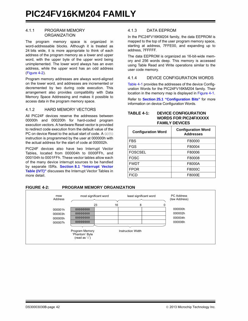
PIC24FV16KM204 FAMILY
4.1.1 PROGRAM MEMORY ORGANIZATION
The program memory space is organized inword-addressable blocks. Although it is treated as24 bits wide, it is more appropriate to think of eachaddress of the program memory as a lower and upperword, with the upper byte of the upper word beingunimplemented. The lower word always has an evenaddress, while the upper word has an odd address(Figure 4-2).
Program memory addresses are always word-alignedon the lower word, and addresses are incremented ordecremented by two during code execution. Thisarrangement also provides compatibility with DataMemory Space Addressing and makes it possible toaccess data in the program memory space.
4.1.2 HARD MEMORY VECTORS
All PIC24F devices reserve the addresses between00000h and 000200h for hard-coded programexecution vectors. A hardware Reset vector is providedto redirect code execution from the default value of thePC on device Reset to the actual start of code. A GOTOinstruction is programmed by the user at 000000h withthe actual address for the start of code at 000002h.
PIC24F devices also have two Interrupt VectorTables, located from 000004h to 0000FFh, and000104h to 0001FFh. These vector tables allow eachof the many device interrupt sources to be handledby separate ISRs. Section 8.1 “Interrupt VectorTable (IVT)” discusses the Interrupt Vector Tables inmore detail.
4.1.3 DATA EEPROM
In the PIC24FV16KM204 family, the data EEPROM ismapped to the top of the user program memory space,starting at address, 7FFE00, and expanding up toaddress, 7FFFFF.
The data EEPROM is organized as 16-bit-wide mem-ory and 256 words deep. This memory is accessedusing Table Read and Write operations similar to theuser code memory.
4.1.4 DEVICE CONFIGURATION WORDS
Table 4-1 provides the addresses of the device Config-uration Words for the PIC24FV16KM204 family. Theirlocation in the memory map is displayed in Figure 4-1.
Refer to Section 25.1 “Configuration Bits” for moreinformation on device Configuration Words.
TABLE 4-1: DEVICE CONFIGURATION WORDS FOR PIC24FXXXXX FAMILY DEVICES
FIGURE 4-2: PROGRAM MEMORY ORGANIZATION
Configuration WordConfiguration Word
Addresses
FBS F80000
FGS F80004
FOSCSEL F80006
FOSC F80008
FWDT F8000A
FPOR F8000C
FICD F8000E
0816
PC Address
000000h
000002h
000004h
000006h
23
0000000000000000
0000000000000000
Program Memory‘Phantom’ Byte
(read as ‘0’)
least significant wordmost significant word
Instruction Width
000001h
000003h
000005h000007h
mswAddress (lsw Address)
DS30003030B-page 42 2013 Microchip Technology Inc.
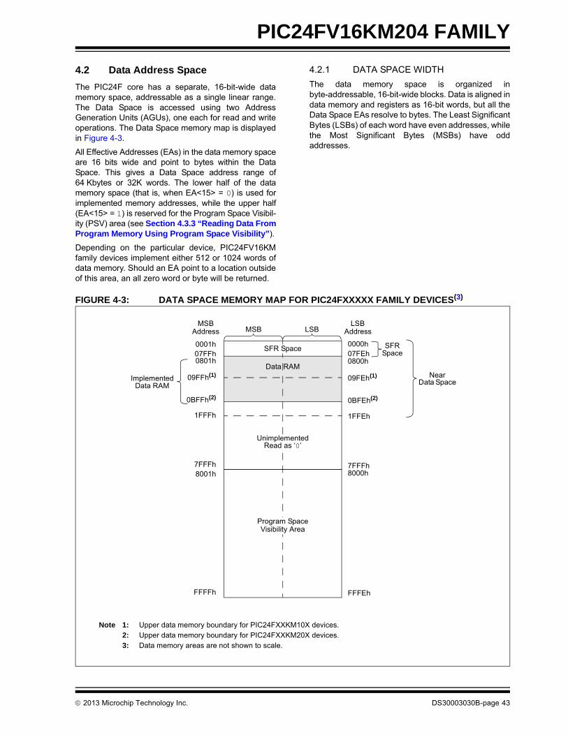
PIC24FV16KM204 FAMILY
4.2 Data Address Space
The PIC24F core has a separate, 16-bit-wide datamemory space, addressable as a single linear range.The Data Space is accessed using two AddressGeneration Units (AGUs), one each for read and writeoperations. The Data Space memory map is displayedin Figure 4-3.
All Effective Addresses (EAs) in the data memory spaceare 16 bits wide and point to bytes within the DataSpace. This gives a Data Space address range of64 Kbytes or 32K words. The lower half of the datamemory space (that is, when EA<15> = 0) is used forimplemented memory addresses, while the upper half(EA<15> = 1) is reserved for the Program Space Visibil-ity (PSV) area (see Section 4.3.3 “Reading Data FromProgram Memory Using Program Space Visibility”).
Depending on the particular device, PIC24FV16KMfamily devices implement either 512 or 1024 words ofdata memory. Should an EA point to a location outsideof this area, an all zero word or byte will be returned.
4.2.1 DATA SPACE WIDTH
The data memory space is organized inbyte-addressable, 16-bit-wide blocks. Data is aligned indata memory and registers as 16-bit words, but all theData Space EAs resolve to bytes. The Least SignificantBytes (LSBs) of each word have even addresses, whilethe Most Significant Bytes (MSBs) have oddaddresses.
FIGURE 4-3: DATA SPACE MEMORY MAP FOR PIC24FXXXXX FAMILY DEVICES(3)
0000h07FEh
FFFEh
LSBAddressLSBMSB
MSBAddress
0001h07FFh
0BFFh(2)
FFFFh
8001h 8000h7FFFh
0801h 0800h
Near
0BFEh(2)
SFRSFR Space
7FFFh
Program SpaceVisibility Area
Note 1: Upper data memory boundary for PIC24FXXKM10X devices.2: Upper data memory boundary for PIC24FXXKM20X devices.3: Data memory areas are not shown to scale.
1FFEh1FFFh
Space
Data SpaceImplementedData RAM
UnimplementedRead as ‘0’
09FFh(1) 09FEh(1)
Data RAM
2013 Microchip Technology Inc. DS30003030B-page 43

PIC24FV16KM204 FAMILY
4.2.2 DATA MEMORY ORGANIZATION AND ALIGNMENT
To maintain backward compatibility with PIC® devicesand improve Data Space memory usage efficiency, thePIC24F instruction set supports both word and byteoperations. As a consequence of byte accessibility, allEA calculations are internally scaled to step throughword-aligned memory. For example, the core recog-nizes that Post-Modified Register Indirect Addressingmode [Ws++] will result in a value of Ws + 1 for byteoperations and Ws + 2 for word operations.
Data byte reads will read the complete word, whichcontains the byte, using the LSB of any EA todetermine which byte to select. The selected byte isplaced onto the LSB of the data path. That is, the datamemory and the registers are organized as twoparallel, byte-wide entities with shared (word) addressdecode, but separate write lines. Data byte writes onlywrite to the corresponding side of the array or register,which matches the byte address.
All word accesses must be aligned to an even address.Misaligned word data fetches are not supported, socare must be taken when mixing byte and wordoperations, or translating from 8-bit MCU code. If a mis-aligned read or write is attempted, an address errortrap will be generated. If the error occurred on a read,the instruction underway is completed; if it occurred ona write, the instruction will be executed, but the writewill not occur. In either case, a trap is then executed,allowing the system and/or user to examine themachine state prior to execution of the address Fault.
All byte loads into any W register are loaded into theLSB; the MSB is not modified.
A Sign-Extend (SE) instruction is provided to allow theusers to translate 8-bit signed data to 16-bit signedvalues. Alternatively, for 16-bit unsigned data, userscan clear the MSB of any W register by executing aZero-Extend (ZE) instruction on the appropriateaddress.
Although most instructions are capable of operating onword or byte data sizes, it should be noted that someinstructions operate only on words.
4.2.3 NEAR DATA SPACE
The 8-Kbyte area between 0000h and 1FFFh is referredto as the Near Data Space. Locations in this space aredirectly addressable via a 13-bit absolute address fieldwithin all memory direct instructions. The remainder ofthe Data Space is addressable indirectly. Additionally,the whole Data Space is addressable using MOV instruc-tions, which support Memory Direct Addressing (MDA)with a 16-bit address field. For PIC24FV16KM204 familydevices, the entire implemented data memory lies inNear Data Space (NDS).
4.2.4 SFR SPACE
The first 2 Kbytes of the Near Data Space, from 0000hto 07FFh, are primarily occupied with Special FunctionRegisters (SFRs). These are used by the PIC24F coreand peripheral modules for controlling the operation ofthe device.
SFRs are distributed among the modules that theycontrol and are generally grouped together by thatmodule. Much of the SFR space contains unusedaddresses; these are read as ‘0’. The SFR space,where the SFRs are actually implemented, is providedin Table 4-2. Each implemented area indicates a32-byte region where at least one address isimplemented as an SFR. A complete listing ofimplemented SFRs, including their addresses, isprovided in Table 4-3 through Table 4-26.
TABLE 4-2: IMPLEMENTED REGIONS OF SFR DATA SPACE
SFR Space Address
xx00 xx20 xx40 xx60 xx80 xxA0 xxC0 xxE0
000h Core ICN Interrupts —
100h Timers CLC MCCP/SCCP
200h MSSP UART Op Amp DAC — — I/O
300h A/D/CMTU — — — —
400h — — — — — — — ANSEL
500h — — — — — — — —
600h — RTCC/Comp — Band Gap —
700h — — System/HLVD
NVM/PMD — — — —
Legend: — = No implemented SFRs in this block.
DS30003030B-page 44 2013 Microchip Technology Inc.

2
01
3 M
icroch
ip T
ech
no
log
y Inc.
D
S3
00
03
03
0B
-pa
ge
45
PIC
24FV
16KM
204 FA
MIL
Y
TA
Nit 3 Bit 2 Bit 1 Bit 0
All Resets
WR 0000
WR 0000
WR 0000
WR 0000
WR 0000
WR 0000
WR 0000
WR 0000
WR 0000
WR 0000
WR 0000
WR 0000
WR 0000
WR 0000
WR 0000
WR 0800
SP xxxx
PC 0000
PC CH3 PCH2 PCH1 PCH0 0000
TB LPAG3 TBLPAG2 TBLPAG1 TBLPAG0 0000
PS VPAG3 PSVPAG2 PSVPAG1 PSVPAG0 0000
RC xxxx
SR N OV Z C 0000
CO IPL3 PSV — — 0000
DIS ICNT3 DISICNT2 DISICNT1 DISICNT0 xxxx
Le
BLE 4-3: CPU CORE REGISTERS MAP
File ame
Addr. Bit 15 Bit 14 Bit 13 Bit 12 Bit 11 Bit 10 Bit 9 Bit 8 Bit 7 Bit 6 Bit 5 Bit 4 B
EG0 0h WREG0
EG1 2h WREG1
EG2 4h WREG2
EG3 6h WREG3
EG4 8h WREG4
EG5 Ah WREG5
EG6 Ch WREG6
EG7 Eh WREG7
EG8 10h WREG8
EG9 12h WREG9
EG10 14h WREG10
EG11 16h WREG11
EG12 18h WREG12
EG13 1Ah WREG13
EG14 1Ch WREG14
EG15 1Eh WREG15
LIM 20h SPLIM Register
L 2Eh PCL Register
H 30h — — — — — — — — PCH7 PCH6 PCH5 PCH4 P
LPAG 32h — — — — — — — — TBLPAG7 TBLPAG6 TBLPAG5 TBLPAG4 TB
VPAG 34h — — — — — — — — PSVPAG7 PSVPAG6 PSVPAG5 PSVPAG4 PS
OUNT 36h RCOUNT Register
42h — — — — — — — DC IPL2 IPL1 IPL0 RA
RCON 44h — — — — — — — — — — — —
ICNT 52h — — DISICNT13 DISICNT12 DISICNT11 DISICNT10 DISICNT9 DISICNT8 DISICNT7 DISICNT6 DISICNT5 DISICNT4 DIS
gend: x = unknown, u = unchanged, — = unimplemented, q = value depends on condition, r = reserved.

PIC
24FV
16KM
204 FA
MIL
Y
DS
30
00
30
30
B-p
ag
e 4
6
2
01
3 M
icroch
ip T
ech
no
log
y Inc.
Bit 3 Bit 2 Bit 1 Bit 0All
Resets
CN3PDE CN2PDE CN1PDE CN0PDE 0000) CN19PDE(2) CN18PDE(2) CN17PDE(2) CN16PDE(1,2) 0000) CN35PDE(2) CN34PDE(2) CN33PDE(2) CN32PDE(2) 0000
CN3IE CN2IE CN1IE CN0IE 0000
CN19IE(2) CN18IE(2) CN17IE(2) CN16IE(1,2) 0000
CN35IE(2) CN34IE(2) CN33IE(2) CN32IE(2) 0000
CN3PUE CN2PUE CN1PUE CN0PUE 0000) CN19PUE(2) CN18PUE(2) CN17PUE(2) CN16PUE(1,2) 0000) CN35PUE(2) CN34PUE(2) CN33PUE(2) CN32PUE(2) 0000
TABLE 4-4: ICN REGISTER MAP
File Name
Addr. Bit 15 Bit 14 Bit 13 Bit 12 Bit 11 Bit 10 Bit 9 Bit 8 Bit 7 Bit 6 Bit 5 Bit 4
CNPD1 56h CN15PDE(1,2) CN14PDE CN13PDE CN12PDE CN11PDE CN10PDE(2) CN9PDE(1,2) — CN7PDE(1,2) CN6PDE CN5PDE CN4PDE
CNPD2 58h CN31PDE(2) CN30PDE CN29PDE CN28PDE(2) CN27PDE(1,2) CN26PDE(2) CN25PDE(2) CN24PDE(1,2) CN23PDE CN22PDE CN21PDE CN20PDE(2
CNPD3 5Ah — — — — — — — — — — — CN36PDE(2
CNEN1 62h CN15IE(1,2) CN14IE CN13IE CN12IE CN11IE CN10IE(2) CN9IE(1,2) — CN7IE(1,2) CN6IE CN5IE CN4IE
CNEN2 64h CN31IE(2) CN30IE CN29IE CN28IE(2) CN27IE(1,2) CN26IE(2) CN25IE(2) CN24IE(1,2) CN23IE CN22IE CN21IE CN20IE(2)
CNEN3 66h — — — — — — — — — — — CN36IE(2)
CNPU1 6Eh CN15PUE(1,2) CN14PUE CN13PUE CN12PUE CN11PUE CN10PUE(2) CN9PUE(1,2) — CN7PUE(1,2) CN6PUE CN5PUE CN4PUE
CNPU2 70h CN31PUE(2) CN30PUE CN29PUE CN28PUE(2) CN27PUE(1,2) CN26PUE(2) CN25PUE(2) CN24PUE(1,2) CN23PUE CN22PUE CN21PUE CN20PUE(2
CNPU3 72h — — — — — — — — — — — CN36PUE(2
Legend: x = unknown, u = unchanged, — = unimplemented, q = value depends on condition, r = reserved.Note 1: These bits are available only on 28-pin devices
2: These bits are available only on 44-pin devices

2
01
3 M
icroch
ip T
ech
no
log
y Inc.
D
S3
00
03
03
0B
-pa
ge
47
PIC
24FV
16KM
204 FA
MIL
Y
TA
Fi Bit 2 Bit 1 Bit 0All
Resets
IN RR STKERR OSCFAIL — 0000
IN INT2EP INT1EP INT0EP 0000
IF CCP2IF CCP1IF INT0IF 0000
IF CMIF BCL1IF SSP1IF 0000
IF — — — 0000
IF BCL2IF SSP2IF — 0000
IF U2ERIF U1ERIF — 0000
IF — — ULPWUIF 0000
IF — CLC2IF CLC1IF 0000
IE CCP2IE CCP1IE INT0IE 0000
IE CMIE BCL1IE SSP1IE 0000
IE — — — 0000
IE BCL2IE SSP2IE — 0000
IE U2ERIE U1ERIE — 0000
IE — — ULPWUIE 0000
IE — CLC2IE CLC1IE 0000
IP INT0IP2 INT0IP1 INT0IP0 4444
IP — — — 4440
IP CCT2IP2 CCT2IP1 CCT2IP0 4004
IP U1TXIP2 U1TXIP1 U1TXIP0 4044
IP SSP1IP2 SSP1IP1 SSP1IP0 4444
IP INT1IP2 INT1IP1 INT1IP0 0404
IP — — — 4000
IP CCT4IP2 CCT4IP1 CCT4IP0 4444
IP — — — 0040
IP — — — 0440
IP — — — 0400
IP — — — 0440
IP HLVDIP2 HLVDIP1 HLVDIP0 0004
IP — — — 4440
IP ULPWUIP2 ULPWUIP1 ULPWUIP0 0004
IP CLC1IP2 CLC1IP1 CLC1IP0 0044
IN M3 VECNUM2 VECNUM1 VECNUM0 0000
Le
BLE 4-5: INTERRUPT CONTROLLER REGISTER MAP
le Name Addr. Bit 15 Bit 14 Bit 13 Bit 12 Bit 11 Bit 10 Bit 9 Bit 8 Bit 7 Bit 6 Bit 5 Bit 4 Bit 3
TCON1 80h NSTDIS — — — — — — — — — — MATHERR ADDRE
TCON2 82h ALTIVT DISI — — — — — — — — — — —
S0 84h NVMIF — AD1IF U1TXIF U1RXIF — — CCT2IF CCT1IF CCP4IF CCP3IF — T1IF
S1 86h U2TXIF U2RXIF INT2IF CCT4IF CCT3IF — — — — CCP5IF — INT1IF CNIF
S2 88h — — — — — — CCT5IF — — — — — —
S3 8Ah — RTCIF — — — — — — — — — — —
S4 8Ch DAC2IF DAC1IF CTMUIF — — — — HLVDIF — — — — —
S5 8Eh — — — — — — — — — — — — —
S6 90h — — — — — — — — — — — — —
C0 94h NVMIE — AD1IE U1TXIE U1RXIE — — CCT2IE CCT1IE CCP4IE CCP3IE — T1IE
C1 96h U2TXIE U2RXIE INT2IE CCT4IE CCT3IE — — — — CCP5IE — INT1IE CNIE
C2 98h — — — — — — CCT5IE — — — — — —
C3 9Ah — RTCIE — — — — — — — — — — —
C4 9Ch DAC2IE DAC1IE CTMUIE — — — — HLVDIE — — — — —
C5 9Eh — — — — — — — — — — — — —
C6 A0h — — — — — — — — — — — — —
C0 A4h — T1IP2 T1IP1 T1IP0 — CCP2IP2 CCP2IP1 CCP2IP0 — CCP1IP2 CCP1IP1 CCP1IP0 —
C1 A6h — CCT1IP2 CCT1IP1 CCT1IP0 — CCP4IP2 CCP4IP1 CCP4IP0 — CCP3IP2 CCP3IP1 CCP3IP0 —
C2 A8h — U1RXIP2 U1RXIP1 U1RXIP0 — — — — — — — — —
C3 AAh — NVMIP2 NVMIP1 NVMIP0 — — — — — AD1IP2 AD1IP1 AD1IP0 —
C4 ACh — CNIP2 CNIP1 CNIP0 — CMIP2 CMIP1 CMIP0 — BCL1IP2 BCL1IP1 BCL1IP0 —
C5 AEh — — — — — CCP5IP2 CCP5IP1 CCP5IP0 — — — — —
C6 B0h — CCT3IP2 CCT3IP1 CCT3IP0 — — — — — — — — —
C7 B2h — U2TXIP2 U2TXIP1 U2TXIP0 — U2RXIP2 U2RXIP1 U2RXIP0 — INT2IP2 INT2IP1 INT2IP0 —
C10 B8h — — — — — — — — — CCT5IP2 CCT5IP1 CCT5IP0 —
C12 BCh — — — — — BCL2IP2 BCL2IP1 BCL2IP0 — SSP2IP2 SSP2IP1 SSP2IP0 —
C15 C2h — — — — — RTCIP2 RTCIP1 RTCIP0 — — — — —
C16 C4h — — — — — U2ERIP2 U2ERIP1 U2ERIP0 — U1ERIP2 U1ERIP1 U1ERIP0 —
C18 C8h — — — — — — — — — — — — —
C19 CAh — DAC2IP2 DAC2IP1 DAC2IP0 — DAC1IP2 DAC1IP1 DAC1IP0 — CTMUIP2 CTMUIP1 CTMUIP0 —
C20 CCh — — — — — — — — — — — — —
C24 D4h — — — — — — — — — CLC2IP2 CLC2IP1 CLC2IP0 —
TTREG E0h CPUIRQ — VHOLD — ILR3 ILR2 ILR1 ILR0 — VECNUM6 VECNUM5 VECNUM4 VECNU
gend: x = unknown, u = unchanged, — = unimplemented, q = value depends on condition, r = reserved.

PIC
24FV
16KM
204 FA
MIL
Y
DS
30
00
30
30
B-p
ag
e 4
8
2
01
3 M
icroch
ip T
ech
no
log
y Inc.
Bit 3 Bit 2 Bit 1 Bit 0All
Resets
xxxx
FFFF
— TSYNC TCS — 0000
Bit 3 Bit 2 Bit 1 Bit 0All
Resets
— MODE2 MODE1 MODE0 0000
4POL G3POL G2POL G1POL 0000
— DS12 DS11 DS10 0000
1D2T G1D2N G1D1T G1D1N 0000
3D2T G3D2N G3D1T G3D1N 0000
— MODE2 MODE1 MODE0 0000
4POL G3POL G2POL G1POL 0000
— DS12 DS11 DS10 0000
1D2T G1D2N G1D1T G1D1N 0000
3D2T G3D2N G3D1T G3D1N 0000
TABLE 4-6: TIMER1 REGISTER MAP
File Name Addr. Bit 15 Bit 14 Bit 13 Bit 12 Bit 11 Bit 10 Bit 9 Bit 8 Bit 7 Bit 6 Bit 5 Bit 4
TMR1 100h Timer1 Register
PR1 102h Timer1 Period Register
T1CON 104h TON — TSIDL — — — TECS1 TECS0 — TGATE TCKPS1 TCKPS0
Legend: x = unknown, u = unchanged, — = unimplemented, q = value depends on condition, r = reserved.
TABLE 4-7: CLC1-2 REGISTER MAP
File Name Addr. Bit 15 Bit 14 Bit 13 Bit 12 Bit 11 Bit 10 Bit 9 Bit 8 Bit 7 Bit 6 Bit 5 Bit 4
CLC1CONL 122h LCEN — — — INTP INTN — — LCOE LCOUT LCPOL —
CLC1CONH 124h — — — — — — — — — — — — G
CLC1SEL 126h — DS42 DS41 DS40 — DS32 DS31 DS30 — DS22 DS21 DS20
CLC1GLSL 12Ah G2D4T G2D4N G2D3T G2D3N G2D2T G2D2N G2D1T G2D1N G1D4T G1D4N G1D3T G1D3N G
CLC1GLSH 12Ch G4D4T G4D4N G4D3T G4D3N G4D2T G4D2N G4D1T G4D1N G3D4T G3D4N G3D3T G3D3N G
CLC2CONL(1) 12Eh LCEN — — — INTP INTN — — LCOE LCOUT LCPOL —
CLC2CONH(1) 130h — — — — — — — — — — — — G
CLC2SEL(1) 132h — DS42 DS41 DS40 — DS32 DS31 DS30 — DS22 DS21 DS20
CLC2GLSL(1) 136h G2D4T G2D4N G2D3T G2D3N G2D2T G2D2N G2D1T G2D1N G1D4T G1D4N G1D3T G1D3N G
CLC2GLSH(1) 138h G4D4T G4D4N G4D3T G4D3N G4D2T G4D2N G4D1T G4D1N G3D4T G3D4N G3D3T G3D3N G
Legend: x = unknown, u = unchanged, — = unimplemented, q = value depends on condition, r = reserved.Note 1: These registers are available only on PIC24F(V)16KM2XX devices.
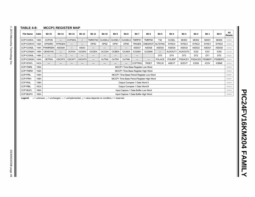
2
01
3 M
icroch
ip T
ech
no
log
y Inc.
D
S3
00
03
03
0B
-pa
ge
49
PIC
24FV
16KM
204 FA
MIL
Y
TA
F Bit 3 Bit 2 Bit 1 Bit 0All
Resets
CC MOD3 MOD2 MOD1 MOD0 0000
CC SYNC3 SYNC2 SYNC1 SYNC0 0000
CC ASDG3 ASDG2 ASDG1 ASDG0 0000
CC UXOUT0 ICS2 ICS1 ICS0 0100
CC DT3 DT2 DT1 DT0 0000
CC SSACE1 PSSACE0 PSSBDF1 PSSBDF0 0000
CC SCEVT ICDIS ICOV ICBNE 0000
CC 0000
CC 0000
CC FFFF
CC FFFF
CC 0000
CC 0000
CC 0000
CC 0000
Leg
BLE 4-8: MCCP1 REGISTER MAP
ile Name Addr. Bit 15 Bit 14 Bit 13 Bit 12 Bit 11 Bit 10 Bit 9 Bit 8 Bit 7 Bit 6 Bit 5 Bit 4
P1CON1L 140h CCPON — CCPSIDL r TMRSYNC CLKSEL2 CLKSEL1 CLKSEL0 TMRPS1 TMRPS0 T32 CCSEL
P1CON1H 142h OPSSRC RTRGEN — — OPS3 OPS2 OPS1 OPS0 TRIGEN ONESHOT ALTSYNC SYNC4
P1CON2L 144h PWMRSEN ASDGM — SSDG — — — — ASDG7 ASDG6 ASDG5 ASDG4
P1CON2H 146h OENSYNC — OCFEN OCEEN OCDEN OCCEN OCBEN OCAEN ICGSM1 ICGSM0 — AUXOUT1 A
P1CON3L 148h — — — — — — — — — DT5 DT4
P1CON3H 14Ah OETRIG OSCNT2 OSCNT1 OSCNT0 — OUTM2 OUTM1 OUTM0 — — POLACE POLBDF P
P1STATL 14Ch — — — — — — — — CCPTRIG TRSET TRCLR ASEVT
P1TMRL 150h MCCP1 Time Base Register Low Word
P1TMRH 152h MCCP1 Time Base Register High Word
P1PRL 154h MCCP1 Time Base Period Register Low Word
P1PRH 156h MCCP1 Time Base Period Register High Word
P1RAL 158h Output Compare 1 Data Word A
P1RBL 15Ch Output Compare 1 Data Word B
P1BUFL 160h Input Capture 1 Data Buffer Low Word
P1BUFH 162h Input Capture 1 Data Buffer High Word
end: x = unknown, u = unchanged, — = unimplemented, q = value depends on condition, r = reserved.

PIC
24FV
16KM
204 FA
MIL
Y
DS
30
00
30
30
B-p
ag
e 5
0
2
01
3 M
icroch
ip T
ech
no
log
y Inc.
Bit 3 Bit 2 Bit 1 Bit 0All
Resets
L MOD3 MOD2 MOD1 MOD0 0000
4 SYNC3 SYNC2 SYNC1 SYNC0 0000
4 ASDG3 ASDG2 ASDG1 ASDG0 0000
T1 AUXOUT0 ICSEL2 ICSEL1 ICSEL0 0100
DT3 DT2 DT1 DT0 0000(1) PSSACE1 PSSACE0 PSSBDF1(1) PSSBDF0(1) 0000
T SCEVT ICDIS ICOV ICBNE 0000
0000
0000
FFFF
FFFF
0000
0000
0000
0000
TABLE 4-9: MCCP2 REGISTER MAP
File Name Addr. Bit 15 Bit 14 Bit 13 Bit 12 Bit 11 Bit 10 Bit 9 Bit 8 Bit 7 Bit 6 Bit 5 Bit 4
CCP2CON1L 164h CCPON — CCPSIDL r TMRSYNC CLKSEL2 CLKSEL1 CLKSEL0 TMRPS1 TMRPS0 T32 CCSE
CCP2CON1H 166h OPSSRC RTRGEN — — IOPS3 IOPS2 IOPS1 IOPS0 TRIGEN ONESHOT ALTSYNC SYNC
CCP2CON2L 168h PWMRSEN ASDGM — SSDG — — — — ASDG7 ASDG6 ASDG5 ASDG
CCP2CON2H 16Ah OENSYNC — OCFEN(1) OCEEN(1) OCDEN(1) OCCEN(1) OCBEN(1) OCAEN ICGSM1 ICGSM0 — AUXOU
CCP2CON3L 16Ch — — — — — — — — — DT5 DT4
CCP2CON3H 16Eh OETRIG OSCNT2 OSCNT1 OSCNT0 — OUTM2(1) OUTM1(1) OUTM0(1) — — POLACE POLBDF
CCP2STATL 170h — — — — — — — — CCPTRIG TRSET TRCLR ASEV
CCP2TMRL 174h MCCP2 Time Base Register Low Word
CCP2TMRH 176h MCCP2 Time Base Register High Word
CCP2PRL 178h MCCP2 Time Base Period Register Low Word
CCP2PRH 17Ah MCCP2 Time Base Period Register High Word
CCP2RAL 17Ch Output Compare 2 Data Word A
CCP2RBL 180h Output Compare 2 Data Word B
CCP2BUFL 184h Input Capture 2 Data Buffer Low Word
CCP2BUFH 186h Input Capture 2 Data Buffer High Word
Legend: x = unknown, u = unchanged, — = unimplemented, q = value depends on condition, r = reserved. Note 1: These bits are available only on PIC24F(V)16KM2XX devices.

2
01
3 M
icroch
ip T
ech
no
log
y Inc.
D
S3
00
03
03
0B
-pa
ge
51
PIC
24FV
16KM
204 FA
MIL
Y
TA
Bit 3 Bit 2 Bit 1 Bit 0All
Resets
CC MOD3 MOD2 MOD1 MOD0 0000
CC YNC3 SYNC2 SYNC1 SYNC0 0000
CC SDG3 ASDG2 ASDG1 ASDG0 0000
CC XOUT0 ICS2 ICS1 ICS0 0100
CC DT3 DT2 DT1 DT0 0000
CC SACE1 PSSACE0 PSSBDF1 PSSBDF0 0000
CC CEVT ICDIS ICOV ICBNE 0000
CC 0000
CC 0000
CC FFFF
CC FFFF
CC 0000
CC 0000
CC 0000
CC 0000
LegNo
BLE 4-10: MCCP3 REGISTER MAP
File Name Addr. Bit 15 Bit 14 Bit 13 Bit 12 Bit 11 Bit 10 Bit 9 Bit 8 Bit 7 Bit 6 Bit 5 Bit 4
P3CON1L(1) 188h CCPON — CCPSIDL r TMRSYNC CLKSEL2 CLKSEL1 CLKSEL0 TMRPS1 TMRPS0 T32 CCSEL
P3CON1H(1) 18Ah OPSSRC RTRGEN — — IOPS3 IOPS2 IOPS1 IOPS0 TRIGEN ONESHOT ALTSYNC SYNC4 S
P3CON2L(1) 18Ch PWMRSEN ASDGM — SSDG — — — — ASDG7 ASDG6 ASDG5 ASDG4 A
P3CON2H(1) 18Eh OENSYNC — OCFEN OCEEN OCDEN OCCEN OCBEN OCAEN ICGSM1 ICGSM0 — AUXOUT1 AU
P3CON3L(1) 190h — — — — — — — — — — DT5 DT4
P3CON3H(1) 192h OETRIG OSCNT2 OSCNT1 OSCNT0 — OUTM2 OUTM1 OUTM0 — — POLACE POLBDF PS
P3STAT(1) 194h — — — — — — — — CCPTRIG TRSET TRCLR ASEVT S
P3TMRL(1) 198h MCCP3 Time Base Register Low Word
P3TMRH(1) 19Ah MCCP3 Time Base Register High Word
P3PRL(1) 19Ch MCCP3 Time Base Period Register Low Word
P3PRH(1) 19Eh MCCP3 Time Base Period Register High Word
P3RAL(1) 1A0h Output Compare 3 Data Word A
P3RBL(1) 1A4h Output Compare 3 Data Word B
P3BUFL(1) 1A8h Input Capture 3 Data Buffer Low Word
P3BUFH(1) 1AAh Input Capture 3 Data Buffer High Word
end: x = unknown, u = unchanged, — = unimplemented, q = value depends on condition, r = reserved. te 1: These registers are available only on PIC24F(V)16KM2XX devices.
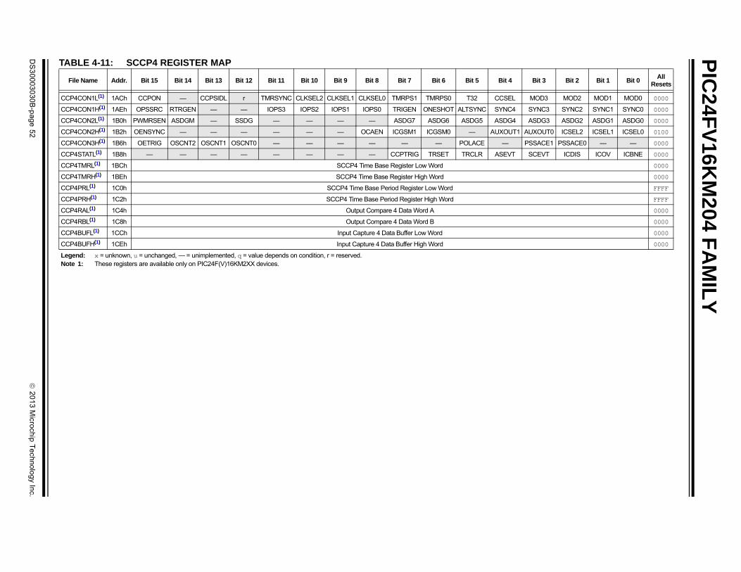
PIC
24FV
16KM
204 FA
MIL
Y
DS
30
00
30
30
B-p
ag
e 5
2
2
01
3 M
icroch
ip T
ech
no
log
y Inc.
it 4 Bit 3 Bit 2 Bit 1 Bit 0All
Resets
SEL MOD3 MOD2 MOD1 MOD0 0000
NC4 SYNC3 SYNC2 SYNC1 SYNC0 0000
DG4 ASDG3 ASDG2 ASDG1 ASDG0 0000
OUT1 AUXOUT0 ICSEL2 ICSEL1 ICSEL0 0100
PSSACE1 PSSACE0 — — 0000
EVT SCEVT ICDIS ICOV ICBNE 0000
0000
0000
FFFF
FFFF
0000
0000
0000
0000
TABLE 4-11: SCCP4 REGISTER MAP
File Name Addr. Bit 15 Bit 14 Bit 13 Bit 12 Bit 11 Bit 10 Bit 9 Bit 8 Bit 7 Bit 6 Bit 5 B
CCP4CON1L(1) 1ACh CCPON — CCPSIDL r TMRSYNC CLKSEL2 CLKSEL1 CLKSEL0 TMRPS1 TMRPS0 T32 CC
CCP4CON1H(1) 1AEh OPSSRC RTRGEN — — IOPS3 IOPS2 IOPS1 IOPS0 TRIGEN ONESHOT ALTSYNC SY
CCP4CON2L(1) 1B0h PWMRSEN ASDGM — SSDG — — — — ASDG7 ASDG6 ASDG5 AS
CCP4CON2H(1) 1B2h OENSYNC — — — — — — OCAEN ICGSM1 ICGSM0 — AUX
CCP4CON3H(1) 1B6h OETRIG OSCNT2 OSCNT1 OSCNT0 — — — — — — POLACE —
CCP4STATL(1) 1B8h — — — — — — — — CCPTRIG TRSET TRCLR AS
CCP4TMRL(1) 1BCh SCCP4 Time Base Register Low Word
CCP4TMRH(1) 1BEh SCCP4 Time Base Register High Word
CCP4PRL(1) 1C0h SCCP4 Time Base Period Register Low Word
CCP4PRH(1) 1C2h SCCP4 Time Base Period Register High Word
CCP4RAL(1) 1C4h Output Compare 4 Data Word A
CCP4RBL(1) 1C8h Output Compare 4 Data Word B
CCP4BUFL(1) 1CCh Input Capture 4 Data Buffer Low Word
CCP4BUFH(1) 1CEh Input Capture 4 Data Buffer High Word
Legend: x = unknown, u = unchanged, — = unimplemented, q = value depends on condition, r = reserved.Note 1: These registers are available only on PIC24F(V)16KM2XX devices.

2
01
3 M
icroch
ip T
ech
no
log
y Inc.
D
S3
00
03
03
0B
-pa
ge
53
PIC
24FV
16KM
204 FA
MIL
Y
TA
F Bit 3 Bit 2 Bit 1 Bit 0All
Resets
CC MOD3 MOD2 MOD1 MOD0 0000
CC SYNC3 SYNC2 SYNC1 SYNC0 0000
CC ASDG3 ASDG2 ASDG1 ASDG0 0000
CC AUXOUT0 ICSEL2 ICSEL1 ICSEL0 0100
CC PSSACE1 PSSACE0 — — 0000
CC SCEVT ICDIS ICOV ICBNE 0000
CC 0000
CC 0000
CC FFFF
CC FFFF
CC 0000
CC 0000
CC 0000
CC 0000
LegNo
BLE 4-12: SCCP5 REGISTER MAP
ile Name Addr. Bit 15 Bit 14 Bit 13 Bit 12 Bit 11 Bit 10 Bit 9 Bit 8 Bit 7 Bit 6 Bit 5 Bit 4
P5CON1L(1) 1D0h CCPON — CCPSIDL r TMRSYNC CLKSEL2 CLKSEL1 CLKSEL0 TMRPS1 TMRPS0 T32 CCSEL
P5CON1H(1) 1D2h OPSSRC RTRGEN — — IOPS3 IOPS2 IOPS1 IOPS0 TRIGEN ONESHOT ALTSYNC SYNC4
P5CON2L(1) 1D4h PWMRSEN ASDGM — SSDG — — — — ASDG7 ASDG6 ASDG5 ASDG4
P5CON2H(1) 1D6h OENSYNC — — — — — — OCAEN ICGSM1 ICGSM0 — AUXOUT1
P5CON3H(1) 1DAh OETRIG OSCNT2 OSCNT1 OSCNT0 — — — — — — POLACE —
P5STATL(1) 1DCh — — — — — — — — CCPTRIG TRSET TRCLR ASEVT
P5TMRL(1) 1E0h SCCP5 Time Base Register Low Word
P5TMRH(1) 1E2h SCCP5 Time Base Register High Word
P5PRL(1) 1E4h SCCP5 Time Base Period Register Low Word
P5PRH(1) 1E6h SCCP5 Time Base Period Register High Word
P5RAL(1) 1E8h Output Compare 5 Data Word A
P5RBL(1) 1ECh Output Compare 5 Data Word B
P5BUFL(1) 1F0h Input Capture 5 Data Buffer Low Word
P5BUFH(1) 1F2h Input Capture 5 Data Buffer High Word
end: x = unknown, u = unchanged, — = unimplemented, q = value depends on condition, r = reserved. te 1: These registers are available only on PIC24F(V)16KM2XX devices.

PIC
24FV
16KM
204 FA
MIL
Y
DS
30
00
30
30
B-p
ag
e 5
4
2
01
3 M
icroch
ip T
ech
no
log
y Inc.
Bit 3 Bit 2 Bit 1 Bit 0All
Resets
ffer/Transmit Register 00xx
SSPM3 SSPM2 SSPM1 SSPM0 0000
RCEN PEN RSEN SEN 0000
SDAHT SBCDE AHEN DHEN 0000
S R/W UA BF 0000
ister in I2C Slave ModeRegister in I2C Master Mode
0000
MSK3 MSK2 MSK1 MSK0 00FF
Bit 3 Bit 2 Bit 1 Bit 0All
Resets
uffer/Transmit Register 00xx
SSPM3 SSPM2 SSPM1 SSPM0 0000
N RCEN PEN RSEN SEN 0000
N SDAHT SBCDE AHEN DHEN 0000
S R/W UA BF 0000
gister in I2C Slave Mode Register in I2C Master Mode
0000
4 MSK3 MSK2 MSK1 MSK0 00FF
TABLE 4-13: MSSP1 (I2C™/SPI) REGISTER MAP
File Name Addr. Bit 15 Bit 14 Bit 13 Bit 12 Bit 11 Bit 10 Bit 9 Bit 8 Bit 7 Bit 6 Bit 5 Bit 4
SSP1BUF 200h — — — — — — — — MSSP1 Receive Bu
SSP1CON1 202h — — — — — — — — WCOL SSPOV SSPEN CKP
SSP1CON2 204h — — — — — — — — GCEN ACKSTAT ACKDT ACKEN
SSP1CON3 206h — — — — — — — — ACKTIM PCIE SCIE BOEN
SSP1STAT 208h — — — — — — — — SMP CKE D/A P
SSP1ADD 20Ah — — — — — — — — MSSP1 Address RegMSSP1 Baud Rate Reload
SSP1MSK 20Ch — — — — — — — — MSK7 MSK6 MSK5 MSK4
Legend: x = unknown, u = unchanged, — = unimplemented, q = value depends on condition, r = reserved.
TABLE 4-14: MSSP2 (I2C™/SPI) REGISTER MAP
File Name Addr. Bit 15 Bit 14 Bit 13 Bit 12 Bit 11 Bit 10 Bit 9 Bit 8 Bit 7 Bit 6 Bit 5 Bit 4
SSP2BUF(1) 210h — — — — — — — — MSSP2 Receive B
SSP2CON1(1) 212h — — — — — — — — WCOL SSPOV SSPEN CKP
SSP2CON2(1) 214h — — — — — — — — GCEN ACKSTAT ACKDT ACKE
SSP2CON3(1) 216h — — — — — — — — ACKTIM PCIE SCIE BOE
SSP2STAT(1) 218h — — — — — — — — SMP CKE D/A P
SSP2ADD(1) 21Ah — — — — — — — — MSSP2 Address ReMSSP2 Baud Rate Reload
SSP2MSK(1) 21Ch — — — — — — — — MSK7 MSK6 MSK5 MSK
Legend: x = unknown, u = unchanged, — = unimplemented, q = value depends on condition, r = reserved. Note 1: These registers are available only on PIC24F(V)16KM2XX devices.
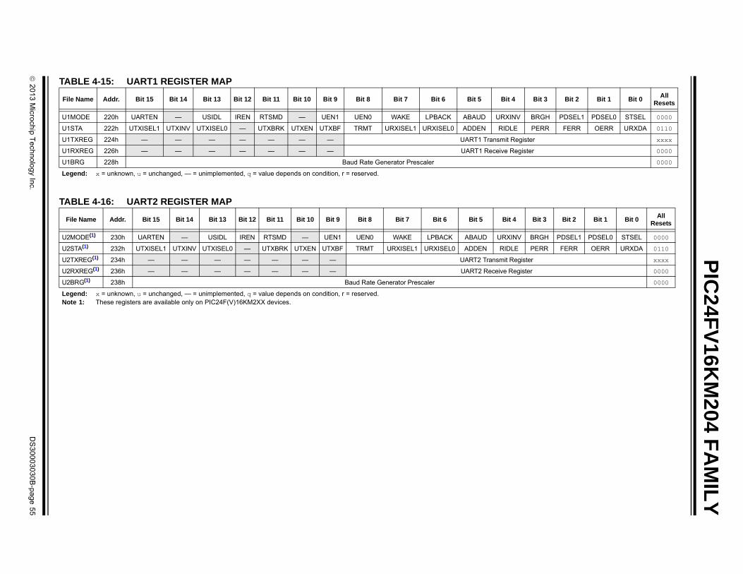
2
01
3 M
icroch
ip T
ech
no
log
y Inc.
D
S3
00
03
03
0B
-pa
ge
55
PIC
24FV
16KM
204 FA
MIL
Y
TA
Fil Bit 3 Bit 2 Bit 1 Bit 0All
Resets
U1 BRGH PDSEL1 PDSEL0 STSEL 0000
U1 PERR FERR OERR URXDA 0110
U1 ster xxxx
U1 ter 0000
U1 0000
Le
TA
F Bit 3 Bit 2 Bit 1 Bit 0All
Resets
U2 BRGH PDSEL1 PDSEL0 STSEL 0000
U2 PERR FERR OERR URXDA 0110
U2 ter xxxx
U2 ter 0000
U2 0000
LeNo
BLE 4-15: UART1 REGISTER MAP
e Name Addr. Bit 15 Bit 14 Bit 13 Bit 12 Bit 11 Bit 10 Bit 9 Bit 8 Bit 7 Bit 6 Bit 5 Bit 4
MODE 220h UARTEN — USIDL IREN RTSMD — UEN1 UEN0 WAKE LPBACK ABAUD URXINV
STA 222h UTXISEL1 UTXINV UTXISEL0 — UTXBRK UTXEN UTXBF TRMT URXISEL1 URXISEL0 ADDEN RIDLE
TXREG 224h — — — — — — — UART1 Transmit Regi
RXREG 226h — — — — — — — UART1 Receive Regis
BRG 228h Baud Rate Generator Prescaler
gend: x = unknown, u = unchanged, — = unimplemented, q = value depends on condition, r = reserved.
BLE 4-16: UART2 REGISTER MAP
ile Name Addr. Bit 15 Bit 14 Bit 13 Bit 12 Bit 11 Bit 10 Bit 9 Bit 8 Bit 7 Bit 6 Bit 5 Bit 4
MODE(1) 230h UARTEN — USIDL IREN RTSMD — UEN1 UEN0 WAKE LPBACK ABAUD URXINV
STA(1) 232h UTXISEL1 UTXINV UTXISEL0 — UTXBRK UTXEN UTXBF TRMT URXISEL1 URXISEL0 ADDEN RIDLE
TXREG(1) 234h — — — — — — — UART2 Transmit Regis
RXREG(1) 236h — — — — — — — UART2 Receive Regis
BRG(1) 238h Baud Rate Generator Prescaler
gend: x = unknown, u = unchanged, — = unimplemented, q = value depends on condition, r = reserved. te 1: These registers are available only on PIC24F(V)16KM2XX devices.

PIC
24FV
16KM
204 FA
MIL
Y
DS
30
00
30
30
B-p
ag
e 5
6
2
01
3 M
icroch
ip T
ech
no
log
y Inc.
Bit 3 Bit 2 Bit 1 Bit 0All
Resets
NINSEL0 PINSEL2 PINSEL1 PINSEL0 0000
Bit 3 Bit 2 Bit 1 Bit 0All
Resets
NINSEL0 PINSEL2 PINSEL1 PINSEL0 0000
t 4 Bit 3 Bit 2 Bit 1 Bit 0All
Resets
SEL2 DACTSEL1 DACTSEL0 DACREF1 DACREF0 0000
AT4(2) DACDAT3(2) DACDAT2(2) DACDAT1(2) DACDAT0(2) 0000
t 4 Bit 3 Bit 2 Bit 1 Bit 0All
Resets
SEL2 DACTSEL1 DACTSEL0 DACREF1 DACREF0 0000
AT4(2) DACDAT3(2) DACDAT2(2) DACDAT1(2) DACDAT0(2) 0000
TABLE 4-17: OP AMP 1 REGISTER MAP
File Name Addr. Bit 15 Bit 14 Bit 13 Bit 12 Bit 11 Bit 10 Bit 9 Bit 8 Bit 7 Bit 6 Bit 5 Bit 4
AMP1CON(1) 24Ah AMPEN — AMPSIDL AMPSLP — — — — SPDSEL — NINSEL2 NINSEL1
Legend: x = unknown, u = unchanged, — = unimplemented, q = value depends on condition, r = reserved. Note 1: This registers are available only on PIC24F(V)16KM2XX devices.
TABLE 4-18: OP AMP 2 REGISTER MAP
File Name Addr. Bit 15 Bit 14 Bit 13 Bit 12 Bit 11 Bit 10 Bit 9 Bit 8 Bit 7 Bit 6 Bit 5 Bit 4
AMP2CON(1) 24Ch AMPEN — AMPSIDL AMPSLP — — — — SPDSEL — NINSEL2 NINSEL1
Legend: x = unknown, u = unchanged, — = unimplemented, q = value depends on condition, r = reserved. Note 1: This registers are available only on PIC24F(V)16KM2XX devices.
TABLE 4-19: DAC1 REGISTER MAP
File Name Addr. Bit 15 Bit 14 Bit 13 Bit 12 Bit 11 Bit 10 Bit 9 Bit 8 Bit 7 Bit 6 Bit 5 Bi
DAC1CON(1) 274h DACEN — DACSIDL DACSLP DACFM — SRDIS DACTRIG DACOE DACTSEL4 DACTSEL3 DACT
DAC1DAT(1) 276h DACDAT15(2) DACDAT14(2) DACDAT13(2) DACDAT12(2) DACDAT11(2) DACDAT10(2) DACDAT9(2) DACDAT8(2) DACDAT7(2) DACDAT6(2) DACDAT5(2) DACD
Legend: x = unknown, u = unchanged, — = unimplemented, q = value depends on condition, r = reserved. Note 1: These registers are available only on PIC24F(V)16KM1XX devices.
2: The 8-bit result format depends on the value of the DACFM control bit.
TABLE 4-20: DAC2 REGISTER MAP
File Name Addr. Bit 15 Bit 14 Bit 13 Bit 12 Bit 11 Bit 10 Bit 9 Bit 8 Bit 7 Bit 6 Bit 5 Bi
DAC2CON(1) 278h DACEN — DACSIDL DACSLP DACFM — SRDIS DACTRIG DACOE DACTSEL4 DACTSEL3 DACT
DAC2DAT(1) 27Ah DACDAT15(2) DACDAT14(2) DACDAT13(2) DACDAT12(2) DACDAT11(2) DACDAT10(2) DACDAT9(2) DACDAT8(2) DACDAT7(2) DACDAT6(2) DACDAT5(2) DACD
Legend: x = unknown, u = unchanged, — = unimplemented, q = value depends on condition, r = reserved. Note 1: These registers are available only on PIC24F(V)16KM2XX devices.
2: The 8-bit result format depends on the value of the DACFM control bit.

2
01
3 M
icroch
ip T
ech
no
log
y Inc.
D
S3
00
03
03
0B
-pa
ge
57
PIC
24FV
16KM
204 FA
MIL
Y
TA
Fil Bit 3 Bit 2 Bit 1 Bit 0All
Resets
TR RISA3 TRISA2 TRISA1 TRISA0 0FDF(1)
PO RA3 RA2 RA1 RA0 xxxx
LA LATA3 LATA2 LATA1 LATA0 xxxx
OD ODA3 ODA2 ODA1 ODA0 0000
LeNo
TA
Fil Bit 3(2) Bit 2 Bit 1 Bit 0All
Resets
TR TRISB3 TRISB2 TRISB1 TRISB0 FFFF(1)
PO RB3 RB2 RB1 RB0 xxxx
LA LATB3 LATB2 LATB1 LATB0 xxxx
OD ODB3 ODB2 ODB1 ODB0 0000
LeNo
TA
Nt 3(2,3) Bit 2(2,3) Bit 1(2,3) Bit 0(2,3) All
Resets
TR ISC3 TRISC2 TRISC1 TRISC0 03FF(1)
PO RC3 RC2 RC1 RC0 xxxx
LA ATC3 LATC2 LATC1 LATC0 xxxx
OD DC3 ODC2 ODC1 ODC0 0000
LeNo
BLE 4-21: PORTA REGISTER MAP
e Name Addr. Bit 15 Bit 14 Bit 13 Bit 12 Bit 11(4,5) Bit 10(4,5) Bit 9(4,5) Bit 8(4,5) Bit 7(4) Bit 6(3) Bit 5(2) Bit 4
ISA 2C0h — — — — TRISA11 TRISA10 TRISA9 TRISA8 TRISA7 TRISA6 — TRISA4 T
RTA 2C2h — — — — RA11 RA10 RA9 RA8 RA7 RA6 RA5 RA4
TA 2C4h — — — — LATA11 LATA10 LATA9 LATA8 LATA7 LATA6 — LATA4
CA 2C6h — — — — ODA11 ODA10 ODA9 ODA8 ODA7 ODA6 — ODA4
gend: x = unknown, u = unchanged, — = unimplemented, q = value depends on condition, r = reserved. te 1: Reset value depends on the device type; the PIC24F16KM204 value is shown.
2: These bits are only available when MCLRE (FPOR<7>) = 0.3: These bits are not implemented in FV devices.4: These bits are not implemented in 20-pin devices.5: These bits are not implemented in 28-pin devices.
BLE 4-22: PORTB REGISTER MAP
e Name Addr. Bit 15 Bit 14 Bit 13 Bit 12 Bit 11(2) Bit 10(2) Bit 9 Bit 8 Bit 7 Bit 6(2) Bit 5(2) Bit 4
ISB 2C8h TRISB15 TRISB14 TRISB13 TRISB12 TRISB11 TRISB10 TRISB9 TRISB8 TRISB7 TRISB6 TRISB5 TRISB4
RTB 2CAh RB15 RB14 RB13 RB12 RB11 RB10 RB9 RB8 RB7 RB6 RB5 RB4
TB 2CCh LATB15 LATB14 LATB13 LATB12 LATB11 LATB10 LATB9 LATB8 LATB7 LATB6 LATB5 LATB4
CB 2CEh ODB15 ODB14 ODB13 ODB12 ODB11 ODB10 ODB9 ODB8 ODB7 ODB6 ODB5 ODB4
gend: x = unknown, u = unchanged, — = unimplemented, q = value depends on condition, r = reserved. te 1: Reset value depends on the device type; the PIC24F16KM204 value is shown.
2: These bits are not implemented in 20-pin devices.
BLE 4-23: PORTC REGISTER MAP
File ame
Addr. Bit 15 Bit 14 Bit 13 Bit 12 Bit 11 Bit 10 Bit 9(2,3) Bit 8(2,3) Bit 7(2,3) Bit 6(2,3) Bit 5(2,3) Bit 4(2,3) Bi
ISC 2D0h — — — — — — TRISC9 TRISC8 TRISC7 TRISC6 TRISC5 TRISC4 TR
RTC 2D2h — — — — — — RC9 RC8 RC7 RC6 RC5 RC4
TTC 2D4h — — — — — — LATC9 LATC8 LATC7 LATC6 LATC5 LATC4 L
CC 2D6h — — — — — — ODC9 ODC8 ODC7 ODC6 ODC5 ODC4 O
gend: x = unknown, u = unchanged, — = unimplemented, q = value depends on condition, r = reserved. te 1: Reset value depends on the device type; the PIC24F16KM204 value is shown.
2: These bits are not implemented in 20-pin devices.3: These bits are not implemented in 28-pin devices.

PIC
24FV
16KM
204 FA
MIL
Y
DS
30
00
30
30
B-p
ag
e 5
8
2
01
3 M
icroch
ip T
ech
no
log
y Inc.
it 4 Bit 3 Bit 2 Bit 1 Bit 0All
Resets
— — — — — 0000
TABLE 4-24: PAD CONFIGURATION REGISTER MAP
File Name Addr. Bit 15 Bit 14 Bit 13 Bit 12 Bit 11 Bit 10 Bit 9 Bit 8 Bit 7 Bit 6 Bit 5 B
PADCFG1 2FCh — — — — SDO2DIS(1) SCK2DIS(1) SDO1DIS SCK1DIS — — —
Legend: x = unknown, u = unchanged, — = unimplemented, q = value depends on condition, r = reserved. Note 1: These bits are not available on the PIC24F(V)08KM101 device, read as ‘0’.

2
01
3 M
icroch
ip T
ech
no
log
y Inc.
D
S3
00
03
03
0B
-pa
ge
59
PIC
24FV
16KM
204 FA
MIL
Y
TA
F Bit 3 Bit 2 Bit 1 Bit 0All
Resets
AD xxxx
AD xxxx
AD xxxx
AD xxxx
AD xxxx
AD xxxx
AD xxxx
AD xxxx
AD xxxx
AD xxxx
AD xxxx
AD xxxx
AD xxxx
AD xxxx
AD xxxx
AD xxxx
AD xxxx
AD xxxx
AD xxxx
AD xxxx
AD xxxx
AD xxxx
AD xxxx
AD xxxx
AD — ASAM SAMP DONE 0000
AD SMPI1 SMPI0 BUFM ALTS 0000
AD ADCS3 ADCS2 ADCS1 ADCS0 0000
AD CH0SA3 CH0SA2 CH0SA1 CH0SA0 0000
AD CSS19(1) CSS18 CSS17 CSS16 0000
AD CSS3 CSS2 CSS1 CSS0 0000
AD WM1 WM0 CM1 CM0 0000
AD CHH19(1) CHH18 CHH17 CHH16 0000
AD CHH3 CHH2 CHH1 CHH0 0000
AD TMEN19(1) CTMEN18 CTMEN17 CTMEN16 0000
AD CTMEN3 CTMEN2 CTMEN1 CTMEN0 0000
LeNo
BLE 4-25: A/D REGISTER MAP
ile Name Addr. Bit 15 Bit 14 Bit 13 Bit 12 Bit 11 Bit 10 Bit 9 Bit 8 Bit 7 Bit 6 Bit 5 Bit 4
C1BUF0 300h A/D Data Buffer 0/Threshold for Channel 0/Threshold for Channel 0 & 12 in Window Compare
C1BUF1 302h A/D Data Buffer 1/Threshold for Channel 1/Threshold for Channel 1 & 13 in Window Compare
C1BUF2 304h A/D Data Buffer 2/Threshold for Channel 2/Threshold for Channel 2 & 14 in Window Compare
C1BUF3 306h A/D Data Buffer 3/Threshold for Channel 3/Threshold for Channel 3 & 15 in Window Compare
C1BUF4 308h A/D Data Buffer 4/Threshold for Channel 4/Threshold for Channel 4 & 16 in Window Compare
C1BUF5 30Ah A/D Data Buffer 5/Threshold for Channel 5/Threshold for Channel 5 & 17 in Window Compare
C1BUF6 30Ch A/D Data Buffer 6/Threshold for Channel 6/Threshold for Channel 6 & 18 in Window Compare
C1BUF7 30Eh A/D Data Buffer 7/Threshold for Channel 7/Threshold for Channel 7 & 19 in Window Compare
C1BUF8 310h A/D Data Buffer 8/Threshold for Channel 8/Threshold for Channel 8 & 20 in Window Compare
C1BUF9 312h A/D Data Buffer 9/Threshold for Channel 9/Threshold for Channel 9 & 21 in Window Compare
C1BUF10 314h A/D Data Buffer 10/Threshold for Channel 10/Threshold for Channel 10 & 22 in Window Compare
C1BUF11 316h A/D Data Buffer 11/Threshold for Channel 11/Threshold for Channel 11 & 23 in Window Compare
C1BUF12 318h A/D Data Buffer 12/Threshold for Channel 12/Threshold for Channel 0 & 12 in Window Compare
C1BUF13 31Ah A/D Data Buffer 13/Threshold for Channel 13/Threshold for Channel 1 & 13 in Window Compare
C1BUF14 31Ch A/D Data Buffer 14/Threshold for Channel 14/Threshold for Channel 2 & 14 in Window Compare
C1BUF15 31Eh A/D Data Buffer 15/Threshold for Channel 15/Threshold for Channel 3 & 15 in Window Compare
C1BUF16 320h A/D Data Buffer 16/Threshold for Channel 16/Threshold for Channel 4 & 16 in Window Compare
C1BUF17 322h A/D Data Buffer 17/Threshold for Channel 17/Threshold for Channel 5 & 17 in Window Compare
C1BUF18 324h A/D Data Buffer 18/Threshold for Channel 18/Threshold for Channel 6 & 18 in Window Compare
C1BUF19 326h A/D Data Buffer 19/Threshold for Channel 19/Threshold for Channel 7 & 19 in Window Compare
C1BUF20 328h A/D Data Buffer 20/Threshold for Channel 20/Threshold for Channel 8 & 20 in Window Compare
C1BUF21 32Ah A/D Data Buffer 21/Threshold for Channel 21/Threshold for Channel 9 & 21 in Window Compare
C1BUF22 32Ch A/D Data Buffer 22/Threshold for Channel 22/Threshold for Channel 10 & 22 in Window Compare
C1BUF23 32Eh A/D Data Buffer 23/Threshold for Channel 23/Threshold for Channel 11 & 23 in Window Compare
1CON1 340h ADON — ADSIDL — — MODE12 FORM1 FORM0 SSRC3 SSRC2 SSRC1 SSRC0
1CON2 342h PVCFG1 PVCFG0 NVCFG0 — BUFREGEN CSCNA — — BUFS SMPI4 SMPI3 SMPI2
1CON3 344h ADRC EXTSAM — SAMC4 SAMC3 SAMC2 SAMC1 SAMC0 ADCS7 ADCS6 ADCS5 ADCS4
1CHS 348h CH0NB2 CH0NB1 CH0NB0 CH0SB4 CH0SB3 CH0SB2 CH0SB1 CH0SB0 CH0NA2 CH0NA1 CH0NA0 CH0SA4
1CSSH 34Eh — CSS30 CSS29 CSS28 CSS27 CSS26 — — CSS23 CSS22 CSS21 CSS20(1)
1CSSL 350h CSS15 CSS14 CSS13 CSS12 CSS11 CSS10 CSS9 CSS8(1,2) CSS7(1,2) CSS6(1,2) CSS5(1) CSS4
1CON5 354h ASEN LPEN CTMREQ BGREQ r — ASINT1 ASINT0 — — — —
1CHITH 356h — — — — — — — — CHH23 CHH22 CHH21 CHH20(1)
1CHITL 358h CHH15 CHH14 CHH13 CHH12 CHH11 CHH10 CHH9 CHH8(1,2) CHH7(1,2) CHH6(1,2) CHH5(1) CHH4
1CTMENH 360h — — — — — — — — CTMEN23 CTMEN22 CTMEN21 CTMEN20(1) C
1CTMENL 362h CTMEN15 CTMEN14 CTMEN13 CTMEN12 CTMEN11 CTMEN10 CTMEN9 CTMEN8((1,2) CTMEN7(1,2) CTMEN6(1,2) CTMEN5(1) CTMEN4
gend: x = unknown, u = unchanged, — = unimplemented, q = value depends on condition, r = reserved. te 1: These bits are not implemented in 20-pin devices.
2: These bits are not implemented in 28-pin devices.

PIC
24FV
16KM
204 FA
MIL
Y
DS
30
00
30
30
B-p
ag
e 6
0
2
01
3 M
icroch
ip T
ech
no
log
y Inc.
it 4 Bit 3 Bit 2 Bit 1 Bit 0All
Resets
IM2 ITRIM1 ITRIM0 IRNG1 IRNG0 0000
2SEL2 EDG2SEL1 EDG2SEL0 — — 0000
TEN — DISCHS2 DISCHS1 DISCHS0 0000
Bit 3 Bit 2 Bit 1 Bit 0All
Resets
NSA3 ANSA2 ANSA1 ANSA0 001F(1)
SB3(2) ANSB2 ANSB1 ANSB0 F3FF(1)
— ANSC2(2,3) ANSC1(2,3) ANSC0(2,3) 0007(1)
Bit 4 Bit 3 Bit 2 Bit 1 Bit 0All
Resets
xxxx
ARPT4 ARPT3 ARPT2 ARPT1 ARPT0 0000(1)
xxxx
CAL4 CAL3 CAL2 CAL1 CAL0 0000(1)
— — — — — 0000(1)
TABLE 4-26: CTMU REGISTER MAP
File Name Addr. Bit 15 Bit 14 Bit 13 Bit 12 Bit 11 Bit 10 Bit 9 Bit 8 Bit 7 Bit 6 Bit 5 B
CTMUCON1L 35Ah CTMUEN — CTMUSIDL TGEN EDGEN EDGSEQEN IDISSEN CTTRIG ITRIM5 ITRIM4 ITRIM3 ITR
CTMUCON1H 35Ch EDG1MOD EDG1POL EDG1SEL3 EDG1SEL2 EDG1SEL1 EDG1SEL0 EDG2STAT EDG1STAT EDG2MOD EDG2POL EDG2SEL3 EDG
CTMUCON2L 35Eh — — — — — — — — — — — IRS
Legend: x = unknown, u = unchanged, — = unimplemented, q = value depends on condition, r = reserved.
TABLE 4-27: ANSEL REGISTER MAP
File Name
Addr. Bit 15 Bit 14 Bit 13 Bit 12 Bit 11 Bit 10 Bit 9 Bit 8 Bit 7 Bit 6 Bit 5 Bit 4
ANSA 4E0h — — — — — — — — — — — ANSA4(2) A
ANSB 4E2h ANSB15 ANSB14 ANSB13 ANSB12 — — ANSB9 ANSB8 ANSB7 ANSB6(2) ANSB5(2) ANSB4 AN
ANSC 4E4h — — — — — — — — — — — —
Legend: x = unknown, u = unchanged, — = unimplemented, q = value depends on condition, r = reserved. Note 1: Reset value depends on the device type; the PIC24F16KM204 value is shown.
2: These bits are not implemented in 20-pin devices.3: These bits are not implemented in 28-pin devices.
TABLE 4-28: REAL-TIME CLOCK AND CALENDAR REGISTER MAP
File Name Addr. Bit 15 Bit 14 Bit 13 Bit 12 Bit 11 Bit 10 Bit 9 Bit 8 Bit 7 Bit 6 Bit 5
ALRMVAL 620h Alarm Value High Register Window Based on APTR<1:0>
ALCFGRPT 622h ALRMEN CHIME AMASK3 AMASK2 AMASK1 AMASK0 ALRMPTR1 ALRMPTR0 ARPT7 ARPT6 ARPT5
RTCVAL 624h RTCC Value High Register Window Based on RTCPTR<1:0>
RCFGCAL 626h RTCEN — RTCWREN RTCSYNC HALFSEC RTCOE RTCPTR1 RTCPTR0 CAL7 CAL6 CAL5
RTCPWC 628h PWCEN PWCPOL PWCCPRE PWCSPRE RTCCLK1 RTCCLK0 RTCOUT1 RTCOUT0 — — —
Legend: x = unknown, u = unchanged, — = unimplemented, q = value depends on condition, r = reserved. Note 1: Values are reset only on a VDD POR event.

2
01
3 M
icroch
ip T
ech
no
log
y Inc.
D
S3
00
03
03
0B
-pa
ge
61
PIC
24FV
16KM
204 FA
MIL
Y
T
Bit 3 Bit 2 Bit 1 Bit 0All
Resets
C — C3OUT(1) C2OUT(1) C1OUT 0000
CVR3 CVR2 CVR1 CVR0 0000
CREF0 — CCH1 CCH0 0000
CREF0 — CCH1 CCH0 0000
CREF0 — CCH1 CCH0 0000
T
3 Bit 2 Bit 1 Bit 0All
Resets
B — BUFREF1 BUFREF0 0001
ABLE 4-29: COMPARATOR REGISTER MAP
File Name Addr. Bit 15 Bit 14 Bit 13 Bit 12 Bit 11 Bit 10 Bit 9 Bit 8 Bit 7 Bit 6 Bit 5 Bit 4
MSTAT 630h CMIDL — — — C3EVT(1) C2EVT(1) C1EVT — — — —
CVRCON 632h — — — — — — — — CVREN CVROE CVRSS CVR4
CM1CON 634h CON COE CPOL CLPWR — — CEVT COUT EVPOL1 EVPOL0 — CREF1
CM2CON(1) 636h CON COE CPOL CLPWR — — CEVT COUT EVPOL1 EVPOL0 — CREF1(1)
CM3CON(1) 638h CON COE CPOL CLPWR — — CEVT COUT EVPOL1 EVPOL0 — CREF1(1)
Legend: x = unknown, u = unchanged, — = unimplemented, q = value depends on condition, r = reserved. Note 1: These registers and bits are available only on PIC24F(V)16KM2XX devices.
ABLE 4-30: BAND GAP BUFFER CONTROL REGISTER MAP
File Name Addr. Bit 15 Bit 14 Bit 13 Bit 12 Bit 11 Bit 10 Bit 9 Bit 8 Bit 7 Bit 6 Bit 5 Bit 4 Bit
UFCON0 670h — — — — — — — — — — — — —
Legend: x = unknown, u = unchanged, — = unimplemented, q = value depends on condition, r = reserved.

PIC
24FV
16KM
204 FA
MIL
Y
DS
30
00
30
30
B-p
ag
e 6
2
2
01
3 M
icroch
ip T
ech
no
log
y Inc.
Bit 3 Bit 2 Bit 1 Bit 0All
Resets
O SLEEP IDLE BOR POR (Note 1)
CF SOSCDRV SOSCEN OSWEN (Note 2)
— — — — 0100
4 TUN3 TUN2 TUN1 TUN0 0000
— — — — 0000
HLVDL3 HLVDL2 HLVDL1 HLVDL0 0000
Bit 3 Bit 2 Bit 1 Bit 0All
Resets
NVMOP3 NVMOP2 NVMOP1 NVMOP0 0000
NVMKEY3 NVMKEY2 NVMKEY1 NVMKEY0 0000
4 Bit 3 Bit 2 Bit 1 Bit 0All
Resets
— — — — 0000
Bit 3 Bit 2 Bit 1 Bit 0All
Resets
— — — ADCMD 0000
P4MD(1) CCP3MD(1) CCP2MD CCP1MD 0000
— — SSP2MD(1) — 0000
FOMD CTMUMD HLVDMD — 0000
P2MD(1) — — — 0000
C2MD(1) CLC1MD — — 0000
TABLE 4-31: CLOCK CONTROL REGISTER MAP
File Name Addr. Bit 15 Bit 14 Bit 13 Bit 12 Bit 11 Bit 10 Bit 9 Bit 8 Bit 7 Bit 6 Bit 5 Bit 4
RCON 740h TRAPR IOPUWR SBOREN RETEN — — CM PMSLP EXTR SWR SWDTEN WDT
OSCCON 742h — COSC2 COSC1 COSC0 — NOSC2 NOSC1 NOSC0 CLKLOCK — LOCK —
CLKDIV 744h ROI DOZE2 DOZE1 DOZE0 DOZEN RCDIV2 RCDIV1 RCDIV0 — — — —
OSCTUN 748h — — — — — — — — — — TUN5 TUN
REFOCON 74Eh ROEN — ROSSLP ROSEL RODIV3 RODIV2 RODIV1 RODIV0 — — — —
HLVDCON 756h HLVDEN — HLSIDL — — — — — VDIR BGVST IRVST —
Legend: x = unknown, u = unchanged, — = unimplemented, q = value depends on condition, r = reserved.Note 1: RCON register Reset values are dependent on the type of Reset.
2: OSCCON register Reset values are dependent on Configuration fuses and by type of Reset.
TABLE 4-32: NVM REGISTER MAP
File Name Addr. Bit 15 Bit 14 Bit 13 Bit 12 Bit 11 Bit 10 Bit 9 Bit 8 Bit 7 Bit 6 Bit 5 Bit 4
NVMCON 760h WR WREN WRERR PGMONLY — — — — — ERASE NVMOP5 NVMOP4
NVMKEY 766h — — — — — — — — NVMKEY7 NVMKEY6 NVMKEY5 NVMKEY4
Legend: x = unknown, u = unchanged, — = unimplemented, q = value depends on condition, r = reserved.
TABLE 4-33: ULTRA LOW-POWER WAKE-UP REGISTER MAP
File Name Addr. Bit 15 Bit 14 Bit 13 Bit 12 Bit 11 Bit 10 Bit 9 Bit 8 Bit 7 Bit 6 Bit 5 Bit
ULPWCON 768h ULPEN — ULPSIDL — — — — ULPSINK — — — —
Legend: x = unknown, u = unchanged, — = unimplemented, q = value depends on condition, r = reserved.
TABLE 4-34: PMD REGISTER MAP
File Name
Addr. Bit 15 Bit 14 Bit 13 Bit 12 Bit 11 Bit 10 Bit 9 Bit 8 Bit 7 Bit 6 Bit 5 Bit 4
PMD1 770h — — — — T1MD — — — SSP1MD U2MD(1) U1MD —
PMD2 772h — — — — — — — — — — — CCP5MD(1) CC
PMD3 774h — — — — — CMPMD RTCCMD — — DAC1MD(1) — —
PMD4 776h — — — — — — — — — ULPWUMD — — RE
PMD6 77Ah — — — — — — — — — — AMP1MD(1) DAC2MD(1) AM
PMD8 77Eh — — — — — — — — — — — — CL
Legend: x = unknown, u = unchanged, — = unimplemented, q = value depends on condition, r = reserved. Note 1: These bits are available only on PIC24F(V)16KM2XX devices.

PIC24FV16KM204 FAMILY
4.2.5 SOFTWARE STACK
In addition to its use as a working register, the W15register in PIC24F devices is also used as a SoftwareStack Pointer. The pointer always points to the firstavailable free word and grows from lower to higheraddresses. It pre-decrements for stack pops andpost-increments for stack pushes, as depicted inFigure 4-4.
For a PC push during any CALL instruction, the MSB ofthe PC is zero-extended before the push, ensuring thatthe MSB is always clear.
The Stack Pointer Limit Value (SPLIM) register,associated with the Stack Pointer, sets an upperaddress boundary for the stack. SPLIM is uninitializedat Reset. As is the case for the Stack Pointer,SPLIM<0> is forced to ‘0’ as all stack operations mustbe word-aligned. Whenever an EA is generated usingW15 as a source or destination pointer, the resultingaddress is compared with the value in SPLIM. If thecontents of the Stack Pointer (W15) and the SPLIMregister are equal, and a push operation is performed,a stack error trap will not occur. The stack error trap willoccur on a subsequent push operation.
Thus, for example, if it is desirable to cause a stackerror trap when the stack grows beyond address, 0DF6in RAM, initialize the SPLIM with the value, 0DF4.
Similarly, a Stack Pointer underflow (stack error) trap isgenerated when the Stack Pointer address is found tobe less than 0800h. This prevents the stack frominterfering with the Special Function Register (SFR)space.
FIGURE 4-4: CALL STACK FRAME
4.3 Interfacing Program and Data Memory Spaces
The PIC24F architecture uses a 24-bit-wide programspace and 16-bit-wide Data Space (DS). The architec-ture is also a modified Harvard scheme, meaning thatdata can also be present in the program space. To usethis data successfully, it must be accessed in a way thatpreserves the alignment of information in both spaces.
Apart from the normal execution, the PIC24Farchitecture provides two methods by which theprogram space can be accessed during operation:
• Using table instructions to access individual bytes or words anywhere in the program space
• Remapping a portion of the program space into the Data Space, PSV
Table instructions allow an application to read or writesmall areas of the program memory. This makes themethod ideal for accessing data tables that need to beupdated from time to time. It also allows access to allbytes of the program word. The remapping methodallows an application to access a large block of data ona read-only basis, which is ideal for look ups from alarge table of static data. It can only access the leastsignificant word (lsw) of the program word.
4.3.1 ADDRESSING PROGRAM SPACE
Since the address ranges for the data and programspaces are 16 and 24 bits, respectively, a method isneeded to create a 23-bit or 24-bit program addressfrom 16-bit data registers. The solution depends on theinterface method to be used.
For table operations, the 8-bit Table Memory PageAddress register (TBLPAG) is used to define a 32K wordregion within the program space. This is concatenatedwith a 16-bit EA to arrive at a full 24-bit program spaceaddress. In this format, the Most Significant bit (MSb) ofTBLPAG is used to determine if the operation occurs inthe user memory (TBLPAG<7> = 0) or the configurationmemory (TBLPAG<7> = 1).
For remapping operations, the 8-bit Program SpaceVisibility Page Address register (PSVPAG) is used todefine a 16K word page in the program space. Whenthe MSb of the EA is ‘1’, PSVPAG is concatenated withthe lower 15 bits of the EA to form a 23-bit programspace address. Unlike the table operations, this limitsremapping operations strictly to the user memory area.
See Table 4-35 and Figure 4-5 to know how the pro-gram EA is created for table operations and remappingaccesses from the data EA. Here, P<23:0> refers to aprogram space word, whereas D<15:0> refers to aData Space word.
Note: A PC push during exception processingwill concatenate the SRL register to theMSB of the PC prior to the push.
Note: A write to the SPLIM register should notbe immediately followed by an indirectread operation using W15.
<Free Word>
PC<15:0>
000000000
015
W15 (before CALL)
W15 (after CALL)
Sta
ck G
row
s To
wa
rds
Hig
her
Add
ress
0000h
PC<22:16>
POP : [--W15]PUSH : [W15++]
2013 Microchip Technology Inc. DS30003030B-page 63

PIC24FV16KM204 FAMILY
TABLE 4-35: PROGRAM SPACE ADDRESS CONSTRUCTION
FIGURE 4-5: DATA ACCESS FROM PROGRAM SPACE ADDRESS GENERATION
Access TypeAccessSpace
Program Space Address
<23> <22:16> <15> <14:1> <0>
Instruction Access(Code Execution)
User 0 PC<22:1> 0
0xx xxxx xxxx xxxx xxxx xxx0
TBLRD/TBLWT(Byte/Word Read/Write)
User TBLPAG<7:0> Data EA<15:0>
0xxx xxxx xxxx xxxx xxxx xxxx
Configuration TBLPAG<7:0> Data EA<15:0>
1xxx xxxx xxxx xxxx xxxx xxxx
Program Space Visibility(Block Remap/Read)
User 0 PSVPAG<7:0>(2) Data EA<14:0>(1)
0 xxxx xxxx xxx xxxx xxxx xxxx
Note 1: Data EA<15> is always ‘1’ in this case, but is not used in calculating the program space address. Bit 15 of the address is PSVPAG<0>.
2: PSVPAG can have only two values (‘00’ to access program memory and FF to access data EEPROM) on the PIC24F16KM family.
0Program Counter
23 Bits
1
PSVPAG
8 Bits
EA
15 Bits
Program Counter(1)
Select
TBLPAG
8 Bits
EA
16 Bits
Byte Select
0
0
1/0
User/Configuration
Table Operations(2)
Program Space Visibility(1)
Space Select
24 Bits
23 Bits
(Remapping)
1/0
0
Note 1: The LSb of program space addresses is always fixed as ‘0’ in order to maintain word alignment of data in the program and Data Spaces.
2: Table operations are not required to be word-aligned. Table Read operations are permitted in the configuration memory space.
DS30003030B-page 64 2013 Microchip Technology Inc.

PIC24FV16KM204 FAMILY
4.3.2 DATA ACCESS FROM PROGRAM MEMORY AND DATA EEPROM MEMORY USING TABLE INSTRUCTIONS
The TBLRDL and TBLWTL instructions offer a directmethod of reading or writing the lower word of anyaddress within the program memory without goingthrough Data Space. It also offers a direct method ofreading or writing a word of any address within dataEEPROM memory. The TBLRDH and TBLWTH instruc-tions are the only method to read or write the upper 8 bitsof a program space word as data.
The PC is incremented by 2 for each successive24-bit program word. This allows program memoryaddresses to directly map to Data Space addresses.Program memory can thus be regarded as two 16-bit,word-wide address spaces, residing side by side, eachwith the same address range. TBLRDL and TBLWTLaccess the space which contains the least significantdata word, and TBLRDH and TBLWTH access the spacewhich contains the upper data byte.
Two table instructions are provided to move byte orword-sized (16-bit) data to and from program space.Both function as either byte or word operations.
1. TBLRDL (Table Read Low): In Word mode, itmaps the lower word of the program spacelocation (P<15:0>) to a data address (D<15:0>).
In Byte mode, either the upper or lower byte ofthe lower program word is mapped to the lowerbyte of a data address. The upper byte isselected when byte select is ‘1’; the lower byteis selected when it is ‘0’.
2. TBLRDH (Table Read High): In Word mode, itmaps the entire upper word of a program address(P<23:16>) to a data address. Note thatD<15:8>, the ‘phantom’ byte, will always be ‘0’.
In Byte mode, it maps the upper or lower byte ofthe program word to D<7:0> of the dataaddress, as above. Note that the data willalways be ‘0’ when the upper ‘phantom’ byte isselected (Byte Select = 1).
In a similar fashion, two table instructions, TBLWTHand TBLWTL, are used to write individual bytes orwords to a program space address. The details oftheir operation are explained in Section 5.0 “FlashProgram Memory”.
For all table operations, the area of program memoryspace to be accessed is determined by the TableMemory Page Address register (TBLPAG). TBLPAGcovers the entire program memory space of thedevice, including user and configuration spaces. WhenTBLPAG<7> = 0, the table page is located in the usermemory space. When TBLPAG<7> = 1, the page islocated in configuration space.
FIGURE 4-6: ACCESSING PROGRAM MEMORY WITH TABLE INSTRUCTIONS
Note: The TBLRDH and TBLWTH instructions are notused while accessing data EEPROM memory.
Note: Only Table Read operations will execute in theconfiguration memory space, and only then, inimplemented areas, such as the Device ID.Table Write operations are not allowed.
081623
00000000
00000000
00000000
00000000
‘Phantom’ Byte
TBLRDH.B (Wn<0> = 0)
TBLRDL.W
TBLRDL.B (Wn<0> = 1)
TBLRDL.B (Wn<0> = 0)
23 15 0
TBLPAG
00
000000h
800000h
002BFEh
Program SpaceData EA<15:0>
The address for the table operation is determined by the data EAwithin the page defined by the TBLPAG register. Only readoperations are provided; write operations are also valid in theuser memory area.
2013 Microchip Technology Inc. DS30003030B-page 65
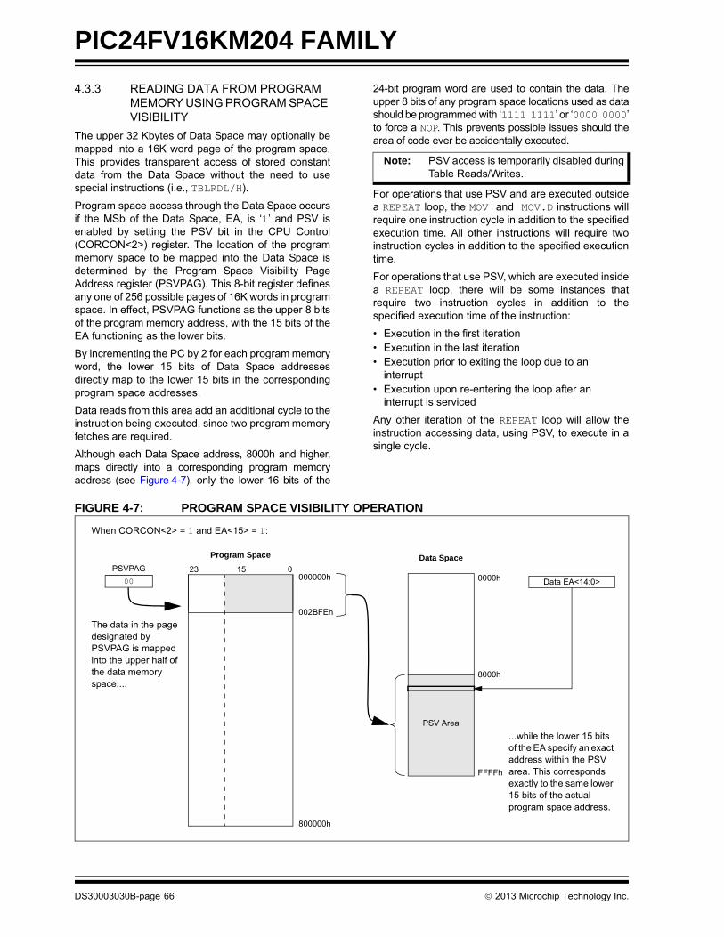
PIC24FV16KM204 FAMILY
4.3.3 READING DATA FROM PROGRAM MEMORY USING PROGRAM SPACE VISIBILITY
The upper 32 Kbytes of Data Space may optionally bemapped into a 16K word page of the program space.This provides transparent access of stored constantdata from the Data Space without the need to usespecial instructions (i.e., TBLRDL/H).
Program space access through the Data Space occursif the MSb of the Data Space, EA, is ‘1’ and PSV isenabled by setting the PSV bit in the CPU Control(CORCON<2>) register. The location of the programmemory space to be mapped into the Data Space isdetermined by the Program Space Visibility PageAddress register (PSVPAG). This 8-bit register definesany one of 256 possible pages of 16K words in programspace. In effect, PSVPAG functions as the upper 8 bitsof the program memory address, with the 15 bits of theEA functioning as the lower bits.
By incrementing the PC by 2 for each program memoryword, the lower 15 bits of Data Space addressesdirectly map to the lower 15 bits in the correspondingprogram space addresses.
Data reads from this area add an additional cycle to theinstruction being executed, since two program memoryfetches are required.
Although each Data Space address, 8000h and higher,maps directly into a corresponding program memoryaddress (see Figure 4-7), only the lower 16 bits of the
24-bit program word are used to contain the data. Theupper 8 bits of any program space locations used as datashould be programmed with ‘1111 1111’ or ‘0000 0000’to force a NOP. This prevents possible issues should thearea of code ever be accidentally executed.
For operations that use PSV and are executed outsidea REPEAT loop, the MOV and MOV.D instructions willrequire one instruction cycle in addition to the specifiedexecution time. All other instructions will require twoinstruction cycles in addition to the specified executiontime.
For operations that use PSV, which are executed insidea REPEAT loop, there will be some instances thatrequire two instruction cycles in addition to thespecified execution time of the instruction:
• Execution in the first iteration• Execution in the last iteration• Execution prior to exiting the loop due to an
interrupt• Execution upon re-entering the loop after an
interrupt is serviced
Any other iteration of the REPEAT loop will allow theinstruction accessing data, using PSV, to execute in asingle cycle.
FIGURE 4-7: PROGRAM SPACE VISIBILITY OPERATION
Note: PSV access is temporarily disabled duringTable Reads/Writes.
23 15 0PSVPAGData SpaceProgram Space
0000h
8000h
FFFFh
00 000000h
800000h
002BFEh
When CORCON<2> = 1 and EA<15> = 1:
PSV Area
The data in the page designated by PSVPAG is mapped into the upper half of the data memory space....
Data EA<14:0>
...while the lower 15 bits of the EA specify an exact address within the PSV area. This corresponds exactly to the same lower 15 bits of the actual program space address.
DS30003030B-page 66 2013 Microchip Technology Inc.

PIC24FV16KM204 FAMILY
5.0 FLASH PROGRAM MEMORY
The PIC24FV16KM204 family of devices containsinternal Flash program memory for storing and execut-ing application code. The memory is readable, writableand erasable when operating with VDD over 1.8V.
Flash memory can be programmed in three ways:
• In-Circuit Serial Programming™ (ICSP™)• Run-Time Self-Programming (RTSP)• Enhanced In-Circuit Serial Programming
(Enhanced ICSP)
ICSP allows a PIC24FXXXXX device to be serially pro-grammed while in the end application circuit. This issimply done with two lines for the programming clockand programming data (which are named PGECx andPGEDx, respectively), and three other lines for power(VDD), ground (VSS) and Master Clear/Program ModeEntry Voltage (MCLR/VPP). This allows customers tomanufacture boards with unprogrammed devices andthen program the microcontroller just before shippingthe product. This also allows the most recent firmwareor custom firmware to be programmed.
Run-Time Self-Programming (RTSP) is accomplishedusing TBLRD (Table Read) and TBLWT (Table Write)instructions. With RTSP, the user may write programmemory data in blocks of 32 instructions (96 bytes) at atime, and erase program memory in blocks of 32, 64 and128 instructions (96,192 and 384 bytes) at a time.
The NVMOP<1:0> (NVMCON<1:0>) bits decide theerase block size.
5.1 Table Instructions and Flash Programming
Regardless of the method used, Flash memoryprogramming is done with the Table Read and Writeinstructions. These allow direct read and write access tothe program memory space from the data memory whilethe device is in normal operating mode. The 24-bit targetaddress in the program memory is formed using theTBLPAG<7:0> bits and the Effective Address (EA) froma W register, specified in the table instruction, asdepicted in Figure 5-1.
The TBLRDL and the TBLWTL instructions are used toread or write to bits<15:0> of program memory.TBLRDL and TBLWTL can access program memory inboth Word and Byte modes.
The TBLRDH and TBLWTH instructions are used to reador write to bits<23:16> of program memory. TBLRDHand TBLWTH can also access program memory in Wordor Byte mode.
FIGURE 5-1: ADDRESSING FOR TABLE REGISTERS
Note: This data sheet summarizes the features ofthis group of PIC24F devices. It is notintended to be a comprehensive referencesource. For more information on Flashprogramming, refer to the “PIC24F FamilyReference Manual”, “Program Memory”(DS39715).
24 Bits
Program
TBLPAG Reg
8 Bits 16 Bits
Using
Byte24-Bit EA
1/0
Select
TableInstruction
Counter
Using
User/ConfigurationSpace Select
Working Reg EA
0Program Counter0
2013 Microchip Technology Inc. DS30003030B-page 67

PIC24FV16KM204 FAMILY
5.2 RTSP Operation
The PIC24F Flash program memory array is organizedinto rows of 32 instructions or 96 bytes. RTSP allowsthe user to erase blocks of 1 row, 2 rows and 4 rows(32, 64 and 128 instructions) at a time, and to programone row at a time. It is also possible to program singlewords.
The 1-row (96 bytes), 2-row (192 bytes) and 4-row(384 bytes) erase blocks, and single row write block(96 bytes) are edge-aligned, from the beginning ofprogram memory.
When data is written to program memory using TBLWTinstructions, the data is not written directly to memory.Instead, data written using Table Writes is stored in holdinglatches until the programming sequence is executed.
Any number of TBLWT instructions can be executedand a write will be successfully performed. However,32 TBLWT instructions are required to write the full rowof memory.
The basic sequence for RTSP programming is to set upa Table Pointer, then do a series of TBLWT instructions toload the buffers. Programming is performed by settingthe control bits in the NVMCON register.
Data can be loaded in any order and the holding regis-ters can be written to multiple times before performinga write operation. Subsequent writes, however, willwipe out any previous writes.
All of the Table Write operations are single-word writes(two instruction cycles), because only the buffers are writ-ten. A programming cycle is required for programmingeach row.
5.3 Enhanced In-Circuit Serial Programming
Enhanced ICSP uses an on-board bootloader, knownas the Program Executive (PE), to manage the pro-gramming process. Using an SPI data frame format,the Program Executive can erase, program and verifyprogram memory. For more information on EnhancedICSP, see the device programming specification.
5.4 Control Registers
There are two SFRs used to read and write theprogram Flash memory: NVMCON and NVMKEY.
The NVMCON register (Register 5-1) controls theblocks that need to be erased, which memory type is tobe programmed and when the programming cyclestarts.
NVMKEY is a write-only register that is used for writeprotection. To start a programming or erase sequence,the user must consecutively write 55h and AAh to theNVMKEY register. Refer to Section 5.5 “ProgrammingOperations” for further details.
5.5 Programming Operations
A complete programming sequence is necessary forprogramming or erasing the internal Flash in RTSPmode. During a programming or erase operation, theprocessor stalls (waits) until the operation is finished.Setting the WR bit (NVMCON<15>) starts theoperation and the WR bit is automatically cleared whenthe operation is finished.
Note: Writing to a location multiple times,without erasing it, is not recommended.
DS30003030B-page 68 2013 Microchip Technology Inc.
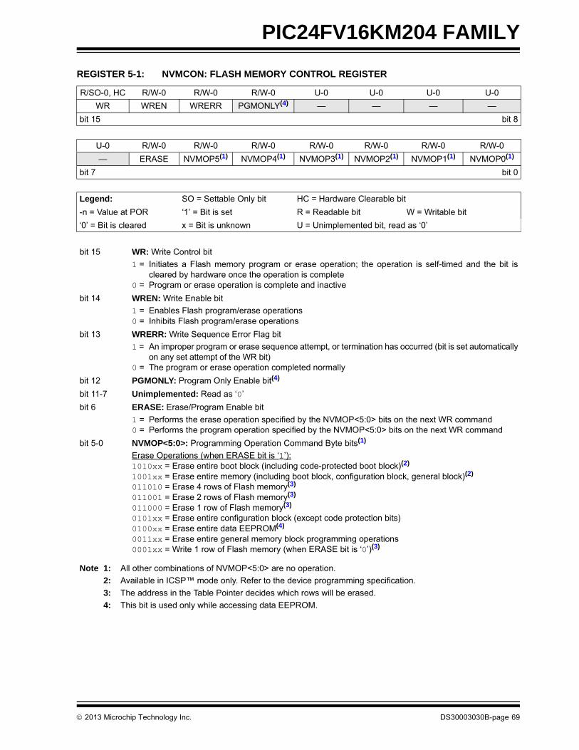
PIC24FV16KM204 FAMILY
REGISTER 5-1: NVMCON: FLASH MEMORY CONTROL REGISTER
R/SO-0, HC R/W-0 R/W-0 R/W-0 U-0 U-0 U-0 U-0
WR WREN WRERR PGMONLY(4) — — — —
bit 15 bit 8
U-0 R/W-0 R/W-0 R/W-0 R/W-0 R/W-0 R/W-0 R/W-0
— ERASE NVMOP5(1) NVMOP4(1) NVMOP3(1) NVMOP2(1) NVMOP1(1) NVMOP0(1)
bit 7 bit 0
Legend: SO = Settable Only bit HC = Hardware Clearable bit
-n = Value at POR ‘1’ = Bit is set R = Readable bit W = Writable bit
‘0’ = Bit is cleared x = Bit is unknown U = Unimplemented bit, read as ‘0’
bit 15 WR: Write Control bit
1 = Initiates a Flash memory program or erase operation; the operation is self-timed and the bit iscleared by hardware once the operation is complete
0 = Program or erase operation is complete and inactive
bit 14 WREN: Write Enable bit
1 = Enables Flash program/erase operations0 = Inhibits Flash program/erase operations
bit 13 WRERR: Write Sequence Error Flag bit
1 = An improper program or erase sequence attempt, or termination has occurred (bit is set automaticallyon any set attempt of the WR bit)
0 = The program or erase operation completed normally
bit 12 PGMONLY: Program Only Enable bit(4)
bit 11-7 Unimplemented: Read as ‘0’
bit 6 ERASE: Erase/Program Enable bit
1 = Performs the erase operation specified by the NVMOP<5:0> bits on the next WR command0 = Performs the program operation specified by the NVMOP<5:0> bits on the next WR command
bit 5-0 NVMOP<5:0>: Programming Operation Command Byte bits(1)
Erase Operations (when ERASE bit is ‘1’):1010xx = Erase entire boot block (including code-protected boot block)(2)
1001xx = Erase entire memory (including boot block, configuration block, general block)(2)
011010 = Erase 4 rows of Flash memory(3)
011001 = Erase 2 rows of Flash memory(3)
011000 = Erase 1 row of Flash memory(3)
0101xx = Erase entire configuration block (except code protection bits)0100xx = Erase entire data EEPROM(4)
0011xx = Erase entire general memory block programming operations0001xx = Write 1 row of Flash memory (when ERASE bit is ‘0’)(3)
Note 1: All other combinations of NVMOP<5:0> are no operation.
2: Available in ICSP™ mode only. Refer to the device programming specification.
3: The address in the Table Pointer decides which rows will be erased.
4: This bit is used only while accessing data EEPROM.
2013 Microchip Technology Inc. DS30003030B-page 69

PIC24FV16KM204 FAMILY
5.5.1 PROGRAMMING ALGORITHM FOR FLASH PROGRAM MEMORY
The user can program one row of Flash programmemory at a time by erasing the programmable row.The general process is:
1. Read a row of program memory (32 instructions)and store in data RAM.
2. Update the program data in RAM with thedesired new data.
3. Erase a row (see Example 5-1):a) Set the NVMOPx bits (NVMCON<5:0>) to
‘011000’ to configure for row erase. Set theERASE (NVMCON<6>) and WREN(NVMCON<14>) bits.
b) Write the starting address of the block to beerased into the TBLPAG and W registers.
c) Write 55h to NVMKEY.d) Write AAh to NVMKEY.e) Set the WR bit (NVMCON<15>). The erase
cycle begins and the CPU stalls for theduration of the erase cycle. When the erase isdone, the WR bit is cleared automatically.
4. Write the first 32 instructions from data RAM intothe program memory buffers (see Example 5-1).
5. Write the program block to Flash memory:
a) Set the NVMOPx bits to ‘000100’ toconfigure for row programming. Clear theERASE bit and set the WREN bit.
b) Write 55h to NVMKEY.c) Write AAh to NVMKEY.d) Set the WR bit. The programming cycle
begins and the CPU stalls for the durationof the write cycle. When the write to Flashmemory is done, the WR bit is clearedautomatically.
For protection against accidental operations, the writeinitiate sequence for NVMKEY must be used to allowany erase or program operation to proceed. After theprogramming command has been executed, the usermust wait for the programming time until programmingis complete. The two instructions following the start ofthe programming sequence should be NOPs, asdisplayed in Example 5-5.
EXAMPLE 5-1: ERASING A PROGRAM MEMORY ROW – ASSEMBLY LANGUAGE CODE
EXAMPLE 5-2: ERASING A PROGRAM MEMORY ROW – ‘C’ LANGUAGE CODE
; Set up NVMCON for row erase operationMOV #0x4058, W0 ;MOV W0, NVMCON ; Initialize NVMCON
; Init pointer to row to be ERASEDMOV #tblpage(PROG_ADDR), W0 ; MOV W0, TBLPAG ; Initialize PM Page Boundary SFRMOV #tbloffset(PROG_ADDR), W0 ; Initialize in-page EA[15:0] pointerTBLWTL W0, [W0] ; Set base address of erase blockDISI #5 ; Block all interrupts
for next 5 instructionsMOV #0x55, W0 MOV W0, NVMKEY ; Write the 55 key MOV #0xAA, W1 ;MOV W1, NVMKEY ; Write the AA keyBSET NVMCON, #WR ; Start the erase sequence NOP ; Insert two NOPs after the eraseNOP ; command is asserted
// C example using MPLAB C30 int __attribute__ ((space(auto_psv))) progAddr = 0x1234; // Variable located in Pgm Memory, declared as a
// global variable unsigned int offset;
//Set up pointer to the first memory location to be written
TBLPAG = __builtin_tblpage(&progAddr); // Initialize PM Page Boundary SFR offset = __builtin_tbloffset(&progAddr); // Initialize lower word of address __builtin_tblwtl(offset, 0x0000); // Set base address of erase block // with dummy latch write NVMCON = 0x4058; // Initialize NVMCON
asm("DISI #5"); // Block all interrupts for next 5 instructions __builtin_write_NVM(); // C30 function to perform unlock // sequence and set WR
DS30003030B-page 70 2013 Microchip Technology Inc.

PIC24FV16KM204 FAMILY
EXAMPLE 5-3: LOADING THE WRITE BUFFERS – ASSEMBLY LANGUAGE CODE
EXAMPLE 5-4: LOADING THE WRITE BUFFERS – ‘C’ LANGUAGE CODE
; Set up NVMCON for row programming operationsMOV #0x4004, W0 ;MOV W0, NVMCON ; Initialize NVMCON
; Set up a pointer to the first program memory location to be written; program memory selected, and writes enabled
MOV #0x0000, W0 ; MOV W0, TBLPAG ; Initialize PM Page Boundary SFRMOV #0x1500, W0 ; An example program memory address
; Perform the TBLWT instructions to write the latches; 0th_program_word
MOV #LOW_WORD_0, W2 ; MOV #HIGH_BYTE_0, W3 ; TBLWTL W2, [W0] ; Write PM low word into program latchTBLWTH W3, [W0++] ; Write PM high byte into program latch
; 1st_program_wordMOV #LOW_WORD_1, W2 ; MOV #HIGH_BYTE_1, W3 ; TBLWTL W2, [W0] ; Write PM low word into program latchTBLWTH W3, [W0++] ; Write PM high byte into program latch
; 2nd_program_wordMOV #LOW_WORD_2, W2 ; MOV #HIGH_BYTE_2, W3 ; TBLWTL W2, [W0] ; Write PM low word into program latchTBLWTH W3, [W0++] ; Write PM high byte into program latch•••
; 32nd_program_wordMOV #LOW_WORD_31, W2 ; MOV #HIGH_BYTE_31, W3 ; TBLWTL W2, [W0] ; Write PM low word into program latchTBLWTH W3, [W0] ; Write PM high byte into program latch
// C example using MPLAB C30
#define NUM_INSTRUCTION_PER_ROW 64int __attribute__ ((space(auto_psv))) progAddr = 0x1234 // Variable located in Pgm Memory
unsigned int offset;unsigned int i;unsigned int progData[2*NUM_INSTRUCTION_PER_ROW]; // Buffer of data to write
//Set up NVMCON for row programmingNVMCON = 0x4004; // Initialize NVMCON
//Set up pointer to the first memory location to be writtenTBLPAG = __builtin_tblpage(&progAddr); // Initialize PM Page Boundary SFRoffset = __builtin_tbloffset(&progAddr); // Initialize lower word of address
//Perform TBLWT instructions to write necessary number of latchesfor(i=0; i < 2*NUM_INSTRUCTION_PER_ROW; i++) __builtin_tblwtl(offset, progData[i++]); // Write to address low word __builtin_tblwth(offset, progData[i]); // Write to upper byte offset = offset + 2; // Increment address
2013 Microchip Technology Inc. DS30003030B-page 71

PIC24FV16KM204 FAMILY
EXAMPLE 5-5: INITIATING A PROGRAMMING SEQUENCE – ASSEMBLY LANGUAGE CODE
EXAMPLE 5-6: INITIATING A PROGRAMMING SEQUENCE – ‘C’ LANGUAGE CODE
DISI #5 ; Block all interrupts for next 5 instructions
MOV #0x55, W0MOV W0, NVMKEY ; Write the 55 key MOV #0xAA, W1 ;MOV W1, NVMKEY ; Write the AA keyBSET NVMCON, #WR ; Start the erase sequence NOP ; 2 NOPs required after setting WRNOP ;BTSC NVMCON, #15 ; Wait for the sequence to be completedBRA $-2 ;
// C example using MPLAB C30
asm("DISI #5"); // Block all interrupts for next 5 instructions
__builtin_write_NVM(); // Perform unlock sequence and set WR
DS30003030B-page 72 2013 Microchip Technology Inc.

PIC24FV16KM204 FAMILY
6.0 DATA EEPROM MEMORY
The data EEPROM memory is a Nonvolatile Memory(NVM), separate from the program and volatile dataRAM. Data EEPROM memory is based on the sameFlash technology as program memory, and is optimizedfor both long retention and a higher number oferase/write cycles.
The data EEPROM is mapped to the top of the user pro-gram memory space, with the top address at programmemory address, 7FFE00h to 7FFFFFh. The size of thedata EEPROM is 256 words in PIC24FXXXXX devices.
The data EEPROM is organized as 16-bit-widememory. Each word is directly addressable, and isreadable and writable during normal operation over theentire VDD range.
Unlike the Flash program memory, normal programexecution is not stopped during a data EEPROMprogram or erase operation.
The data EEPROM programming operations arecontrolled using the three NVM Control registers:
• NVMCON: Nonvolatile Memory Control Register• NVMKEY: Nonvolatile Memory Key Register • NVMADR: Nonvolatile Memory Address Register
6.1 NVMCON Register
The NVMCON register (Register 6-1) is also the primarycontrol register for data EEPROM program/eraseoperations. The upper byte contains the control bitsused to start the program or erase cycle and the flag bitto indicate if the operation was successfully performed.The lower byte of NVMCOM configures the type of NVMoperation that will be performed.
6.2 NVMKEY Register
The NVMKEY is a write-only register that is used toprevent accidental writes or erasures of data EEPROMlocations.
To start any programming or erase sequence, thefollowing instructions must be executed first, in theexact order provided:
1. Write 55h to NVMKEY.
2. Write AAh to NVMKEY.
After this sequence, a write will be allowed to theNVMCON register for one instruction cycle. In mostcases, the user will simply need to set the WR bit in theNVMCON register to start the program or erase cycle.Interrupts should be disabled during the unlocksequence.
The MPLAB® C30 C compiler provides a defined libraryprocedure (builtin_write_NVM) to perform theunlock sequence. Example 6-1 illustrates how theunlock sequence can be performed with in-lineassembly.
EXAMPLE 6-1: DATA EEPROM UNLOCK SEQUENCE
Note: This data sheet summarizes the features ofthis group of PIC24F devices. It is notintended to be a comprehensive referencesource. For more information on dataEEPROM, refer to the “PIC24F FamilyReference Manual”, “Data EEPROM”(DS39720).
//Disable Interrupts For 5 instructions asm volatile ("disi #5");//Issue Unlock Sequenceasm volatile ("mov #0x55, W0 \n"
"mov W0, NVMKEY \n" "mov #0xAA, W1 \n"
"mov W1, NVMKEY \n");// Perform Write/Erase operationsasm volatile ("bset NVMCON, #WR \n"
"nop \n""nop \n");
2013 Microchip Technology Inc. DS30003030B-page 73
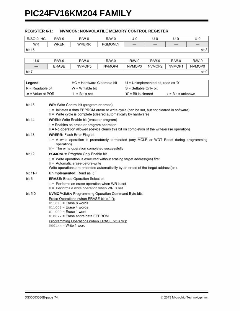
PIC24FV16KM204 FAMILY
REGISTER 6-1: NVMCON: NONVOLATILE MEMORY CONTROL REGISTER
R/SO-0, HC R/W-0 R/W-0 R/W-0 U-0 U-0 U-0 U-0
WR WREN WRERR PGMONLY — — — —
bit 15 bit 8
U-0 R/W-0 R/W-0 R/W-0 R/W-0 R/W-0 R/W-0 R/W-0
— ERASE NVMOP5 NVMOP4 NVMOP3 NVMOP2 NVMOP1 NVMOP0
bit 7 bit 0
Legend: HC = Hardware Clearable bit U = Unimplemented bit, read as ‘0’
R = Readable bit W = Writable bit S = Settable Only bit
-n = Value at POR ‘1’ = Bit is set ‘0’ = Bit is cleared x = Bit is unknown
bit 15 WR: Write Control bit (program or erase)
1 = Initiates a data EEPROM erase or write cycle (can be set, but not cleared in software)0 = Write cycle is complete (cleared automatically by hardware)
bit 14 WREN: Write Enable bit (erase or program)
1 = Enables an erase or program operation0 = No operation allowed (device clears this bit on completion of the write/erase operation)
bit 13 WRERR: Flash Error Flag bit
1 = A write operation is prematurely terminated (any MCLR or WDT Reset during programmingoperation)
0 = The write operation completed successfully
bit 12 PGMONLY: Program Only Enable bit
1 = Write operation is executed without erasing target address(es) first0 = Automatic erase-before-writeWrite operations are preceded automatically by an erase of the target address(es).
bit 11-7 Unimplemented: Read as ‘0’
bit 6 ERASE: Erase Operation Select bit
1 = Performs an erase operation when WR is set0 = Performs a write operation when WR is set
bit 5-0 NVMOP<5:0>: Programming Operation Command Byte bits
Erase Operations (when ERASE bit is ‘1’):011010 = Erase 8 words011001 = Erase 4 words011000 = Erase 1 word 0100xx = Erase entire data EEPROM
Programming Operations (when ERASE bit is ‘0’):0001xx = Write 1 word
DS30003030B-page 74 2013 Microchip Technology Inc.

PIC24FV16KM204 FAMILY
6.3 NVM Address Register
As with Flash program memory, the NVM Addressregisters, NVMADRU and NVMADR, form the 24-bitEffective Address (EA) of the selected row or word fordata EEPROM operations. The NVMADRU register isused to hold the upper 8 bits of the EA, while theNVMADR register is used to hold the lower 16 bits ofthe EA. These registers are not mapped into theSpecial Function Register (SFR) space; instead, theydirectly capture the EA<23:0> of the last Table Writeinstruction that has been executed and select the dataEEPROM row to erase. Figure 6-1 depicts the programmemory EA that is formed for programming and eraseoperations.
Like program memory operations, the Least Significantbit (LSb) of NVMADR is restricted to even addresses.This is because any given address in the data EEPROMspace consists of only the lower word of the programmemory width; the upper word, including the uppermost“phantom byte”, are unavailable. This means that theLSb of a data EEPROM address will always be ‘0’.
Similarly, the Most Significant bit (MSb) of NVMADRUis always ‘0’, since all addresses lie in the user programspace.
FIGURE 6-1: DATA EEPROM ADDRESSING WITH TBLPAG AND NVM ADDRESS REGISTERS
6.4 Data EEPROM Operations
The EEPROM block is accessed using Table Read andWrite operations, similar to those used for programmemory. The TBLWTH and TBLRDH instructions are notrequired for data EEPROM operations since thememory is only 16 bits wide (data on the lower addressis valid only). The following programming operationscan be performed on the data EEPROM:
• Erase one, four or eight words• Bulk erase the entire data EEPROM• Write one word• Read one word
The library procedures are used in the code examplesdetailed in the following sections. General descriptionsof each process are provided for users who are notusing the XC16 compiler libraries.
24-Bit PM Address
TBLPAG
NVMADR
W Register EA
7Fh xxxxh
00
NVMADRU
Note 1: Unexpected results will be obtained if theuser attempts to read the EEPROM whilea programming or erase operation isunderway.
2: The XC16 C compiler includes libraryprocedures to automatically perform theTable Read and Table Write operations,manage the Table Pointer and write buf-fers, and unlock and initiate memorywrite sequences. This eliminates theneed to create assembler macros or timecritical routines in C for each application.
2013 Microchip Technology Inc. DS30003030B-page 75
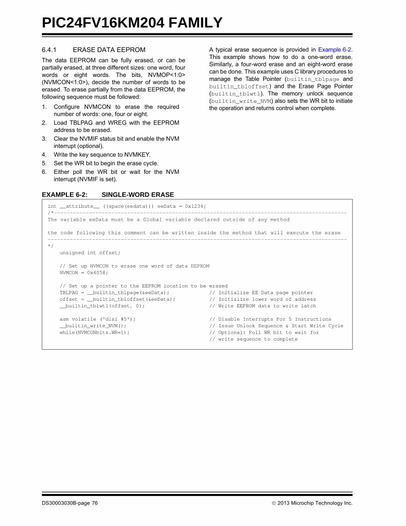
PIC24FV16KM204 FAMILY
6.4.1 ERASE DATA EEPROM
The data EEPROM can be fully erased, or can bepartially erased, at three different sizes: one word, fourwords or eight words. The bits, NVMOP<1:0>(NVMCON<1:0>), decide the number of words to beerased. To erase partially from the data EEPROM, thefollowing sequence must be followed:
1. Configure NVMCON to erase the requirednumber of words: one, four or eight.
2. Load TBLPAG and WREG with the EEPROMaddress to be erased.
3. Clear the NVMIF status bit and enable the NVMinterrupt (optional).
4. Write the key sequence to NVMKEY.
5. Set the WR bit to begin the erase cycle.
6. Either poll the WR bit or wait for the NVMinterrupt (NVMIF is set).
A typical erase sequence is provided in Example 6-2.This example shows how to do a one-word erase.Similarly, a four-word erase and an eight-word erasecan be done. This example uses C library procedures tomanage the Table Pointer (builtin_tblpage andbuiltin_tbloffset) and the Erase Page Pointer(builtin_tblwtl). The memory unlock sequence(builtin_write_NVM) also sets the WR bit to initiatethe operation and returns control when complete.
EXAMPLE 6-2: SINGLE-WORD ERASE
int __attribute__ ((space(eedata))) eeData = 0x1234;/*--------------------------------------------------------------------------------------------The variable eeData must be a Global variable declared outside of any method
the code following this comment can be written inside the method that will execute the erase----------------------------------------------------------------------------------------------*/
unsigned int offset;
// Set up NVMCON to erase one word of data EEPROM NVMCON = 0x4058;
// Set up a pointer to the EEPROM location to be erased TBLPAG = __builtin_tblpage(&eeData); // Initialize EE Data page pointer offset = __builtin_tbloffset(&eeData); // Initizlize lower word of address __builtin_tblwtl(offset, 0); // Write EEPROM data to write latch
asm volatile ("disi #5"); // Disable Interrupts For 5 Instructions__builtin_write_NVM(); // Issue Unlock Sequence & Start Write Cycle while(NVMCONbits.WR=1); // Optional: Poll WR bit to wait for
// write sequence to complete
DS30003030B-page 76 2013 Microchip Technology Inc.
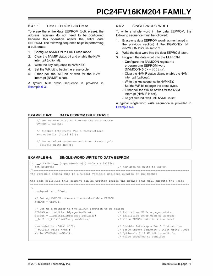
PIC24FV16KM204 FAMILY
6.4.1.1 Data EEPROM Bulk Erase
To erase the entire data EEPROM (bulk erase), theaddress registers do not need to be configuredbecause this operation affects the entire dataEEPROM. The following sequence helps in performinga bulk erase:
1. Configure NVMCON to Bulk Erase mode.
2. Clear the NVMIF status bit and enable the NVMinterrupt (optional).
3. Write the key sequence to NVMKEY.
4. Set the WR bit to begin the erase cycle.
5. Either poll the WR bit or wait for the NVMinterrupt (NVMIF is set).
A typical bulk erase sequence is provided inExample 6-3.
6.4.2 SINGLE-WORD WRITE
To write a single word in the data EEPROM, thefollowing sequence must be followed:
1. Erase one data EEPROM word (as mentioned inthe previous section) if the PGMONLY bit(NVMCON<12>) is set to ‘1’.
2. Write the data word into the data EEPROM latch.
3. Program the data word into the EEPROM:
- Configure the NVMCON register to program one EEPROM word (NVMCON<5:0> = 0001xx).
- Clear the NVMIF status bit and enable the NVM interrupt (optional).
- Write the key sequence to NVMKEY.- Set the WR bit to begin the erase cycle.- Either poll the WR bit or wait for the NVM
interrupt (NVMIF is set).- To get cleared, wait until NVMIF is set.
A typical single-word write sequence is provided inExample 6-4.
EXAMPLE 6-3: DATA EEPROM BULK ERASE
EXAMPLE 6-4: SINGLE-WORD WRITE TO DATA EEPROM
// Set up NVMCON to bulk erase the data EEPROMNVMCON = 0x4050;
// Disable Interrupts For 5 Instructions asm volatile ("disi #5");
// Issue Unlock Sequence and Start Erase Cycle__builtin_write_NVM();
int __attribute__ ((space(eedata))) eeData = 0x1234;int newData; // New data to write to EEPROM
/*---------------------------------------------------------------------------------------------The variable eeData must be a Global variable declared outside of any method
the code following this comment can be written inside the method that will execute the write-----------------------------------------------------------------------------------------------*/
unsigned int offset;
// Set up NVMCON to erase one word of data EEPROMNVMCON = 0x4004;
// Set up a pointer to the EEPROM location to be erasedTBLPAG = __builtin_tblpage(&eeData); // Initialize EE Data page pointeroffset = __builtin_tbloffset(&eeData); // Initizlize lower word of address__builtin_tblwtl(offset, newData); // Write EEPROM data to write latch
asm volatile ("disi #5"); // Disable Interrupts For 5 Instructions__builtin_write_NVM(); // Issue Unlock Sequence & Start Write Cyclewhile(NVMCONbits.WR=1); // Optional: Poll WR bit to wait for
// write sequence to complete
2013 Microchip Technology Inc. DS30003030B-page 77

PIC24FV16KM204 FAMILY
6.4.3 READING THE DATA EEPROM
To read a word from data EEPROM, the Table Readinstruction is used. Since the EEPROM array is only16 bits wide, only the TBLRDL instruction is needed.The read operation is performed by loading TBLPAGand WREG with the address of the EEPROM location,followed by a TBLRDL instruction.
A typical read sequence, using the TablePointer management (builtin_tblpage andbuiltin_tbloffset) and Table Read(builtin_tblrdl) procedures from the C30compiler library, is provided in Example 6-5.
Program Space Visibility (PSV) can also be used toread locations in the data EEPROM.
EXAMPLE 6-5: READING THE DATA EEPROM USING THE TBLRD COMMANDint __attribute__ ((space(eedata))) eeData = 0x1234;int data; // Data read from EEPROM/*--------------------------------------------------------------------------------------------The variable eeData must be a Global variable declared outside of any method
the code following this comment can be written inside the method that will execute the read----------------------------------------------------------------------------------------------*/
unsigned int offset;
// Set up a pointer to the EEPROM location to be erasedTBLPAG = __builtin_tblpage(&eeData); // Initialize EE Data page pointeroffset = __builtin_tbloffset(&eeData); // Initizlize lower word of addressdata = __builtin_tblrdl(offset); // Write EEPROM data to write latch
DS30003030B-page 78 2013 Microchip Technology Inc.
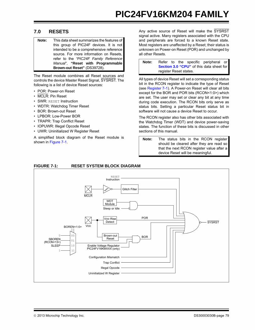
PIC24FV16KM204 FAMILY
7.0 RESETS
The Reset module combines all Reset sources andcontrols the device Master Reset Signal, SYSRST. Thefollowing is a list of device Reset sources:
• POR: Power-on Reset• MCLR: Pin Reset• SWR: RESET Instruction• WDTR: Watchdog Timer Reset• BOR: Brown-out Reset• LPBOR: Low-Power BOR• TRAPR: Trap Conflict Reset• IOPUWR: Illegal Opcode Reset• UWR: Uninitialized W Register Reset
A simplified block diagram of the Reset module isshown in Figure 7-1.
Any active source of Reset will make the SYSRSTsignal active. Many registers associated with the CPUand peripherals are forced to a known Reset state.Most registers are unaffected by a Reset; their status isunknown on Power-on Reset (POR) and unchanged byall other Resets.
All types of device Reset will set a corresponding statusbit in the RCON register to indicate the type of Reset(see Register 7-1). A Power-on Reset will clear all bitsexcept for the BOR and POR bits (RCON<1:0>) whichare set. The user may set or clear any bit at any timeduring code execution. The RCON bits only serve asstatus bits. Setting a particular Reset status bit insoftware will not cause a device Reset to occur.
The RCON register also has other bits associated withthe Watchdog Timer (WDT) and device power-savingstates. The function of these bits is discussed in othersections of this manual.
FIGURE 7-1: RESET SYSTEM BLOCK DIAGRAM
Note: This data sheet summarizes the features ofthis group of PIC24F devices. It is notintended to be a comprehensive referencesource. For more information on Resets,refer to the “PIC24F Family ReferenceManual”, “Reset with ProgrammableBrown-out Reset” (DS39728).
Note: Refer to the specific peripheral orSection 3.0 “CPU” of this data sheet forregister Reset states.
Note: The status bits in the RCON registershould be cleared after they are read sothat the next RCON register value after adevice Reset will be meaningful.
MCLR
VDD
VDD RiseDetect
POR
Sleep or Idle
Brown-outReset
RESETInstruction
WDTModule
Glitch Filter
BOR
Trap Conflict
Illegal Opcode
Uninitialized W Register
SYSRST
BOREN<1:0>
00
01
10
11
0SBOREN
SLEEP
1
Configuration Mismatch
Enable Voltage Regulator(RCON<13>)
PIC24FV16KMXXX (only)
2013 Microchip Technology Inc. DS30003030B-page 79
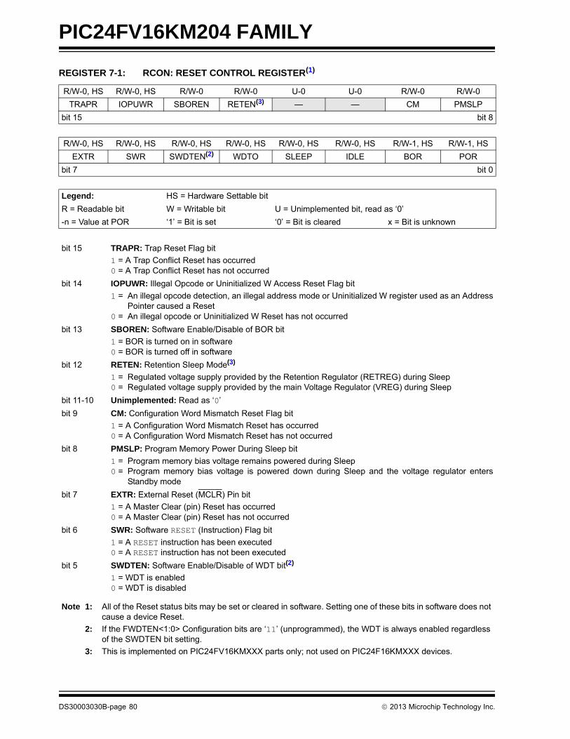
PIC24FV16KM204 FAMILY
REGISTER 7-1: RCON: RESET CONTROL REGISTER(1)
R/W-0, HS R/W-0, HS R/W-0 R/W-0 U-0 U-0 R/W-0 R/W-0
TRAPR IOPUWR SBOREN RETEN(3) — — CM PMSLP
bit 15 bit 8
R/W-0, HS R/W-0, HS R/W-0, HS R/W-0, HS R/W-0, HS R/W-0, HS R/W-1, HS R/W-1, HS
EXTR SWR SWDTEN(2) WDTO SLEEP IDLE BOR POR
bit 7 bit 0
Legend: HS = Hardware Settable bit
R = Readable bit W = Writable bit U = Unimplemented bit, read as ‘0’
-n = Value at POR ‘1’ = Bit is set ‘0’ = Bit is cleared x = Bit is unknown
bit 15 TRAPR: Trap Reset Flag bit
1 = A Trap Conflict Reset has occurred0 = A Trap Conflict Reset has not occurred
bit 14 IOPUWR: Illegal Opcode or Uninitialized W Access Reset Flag bit
1 = An illegal opcode detection, an illegal address mode or Uninitialized W register used as an AddressPointer caused a Reset
0 = An illegal opcode or Uninitialized W Reset has not occurred
bit 13 SBOREN: Software Enable/Disable of BOR bit
1 = BOR is turned on in software0 = BOR is turned off in software
bit 12 RETEN: Retention Sleep Mode(3)
1 = Regulated voltage supply provided by the Retention Regulator (RETREG) during Sleep0 = Regulated voltage supply provided by the main Voltage Regulator (VREG) during Sleep
bit 11-10 Unimplemented: Read as ‘0’
bit 9 CM: Configuration Word Mismatch Reset Flag bit
1 = A Configuration Word Mismatch Reset has occurred0 = A Configuration Word Mismatch Reset has not occurred
bit 8 PMSLP: Program Memory Power During Sleep bit
1 = Program memory bias voltage remains powered during Sleep0 = Program memory bias voltage is powered down during Sleep and the voltage regulator enters
Standby mode
bit 7 EXTR: External Reset (MCLR) Pin bit
1 = A Master Clear (pin) Reset has occurred0 = A Master Clear (pin) Reset has not occurred
bit 6 SWR: Software RESET (Instruction) Flag bit
1 = A RESET instruction has been executed0 = A RESET instruction has not been executed
bit 5 SWDTEN: Software Enable/Disable of WDT bit(2)
1 = WDT is enabled0 = WDT is disabled
Note 1: All of the Reset status bits may be set or cleared in software. Setting one of these bits in software does not cause a device Reset.
2: If the FWDTEN<1:0> Configuration bits are ‘11’ (unprogrammed), the WDT is always enabled regardless of the SWDTEN bit setting.
3: This is implemented on PIC24FV16KMXXX parts only; not used on PIC24F16KMXXX devices.
DS30003030B-page 80 2013 Microchip Technology Inc.

PIC24FV16KM204 FAMILY
TABLE 7-1: RESET FLAG BIT OPERATION
bit 4 WDTO: Watchdog Timer Time-out Flag bit
1 = WDT time-out has occurred0 = WDT time-out has not occurred
bit 3 SLEEP: Wake-up from Sleep Flag bit
1 = Device has been in Sleep mode0 = Device has not been in Sleep mode
bit 2 IDLE: Wake-up from Idle Flag bit
1 = Device has been in Idle mode0 = Device has not been in Idle mode
bit 1 BOR: Brown-out Reset Flag bit
1 = A Brown-out Reset has occurred (the BOR is also set after a POR)0 = A Brown-out Reset has not occurred
bit 0 POR: Power-on Reset Flag bit
1 = A Power-on Reset has occurred0 = A Power-on Reset has not occurred
Flag Bit Setting Event Clearing Event
TRAPR (RCON<15>) Trap Conflict Event POR
IOPUWR (RCON<14>) Illegal Opcode or Uninitialized W Register Access POR
CM (RCON<9>) Configuration Mismatch Reset POR
EXTR (RCON<7>) MCLR Reset POR
SWR (RCON<6>) RESET Instruction POR
WDTO (RCON<4>) WDT Time-out PWRSAV Instruction, POR
SLEEP (RCON<3>) PWRSAV #SLEEP Instruction POR
IDLE (RCON<2>) PWRSAV #IDLE Instruction POR
BOR (RCON<1>) POR, BOR —
POR (RCON<0>) POR —
Note: All Reset flag bits may be set or cleared by the user software.
REGISTER 7-1: RCON: RESET CONTROL REGISTER(1) (CONTINUED)
Note 1: All of the Reset status bits may be set or cleared in software. Setting one of these bits in software does not cause a device Reset.
2: If the FWDTEN<1:0> Configuration bits are ‘11’ (unprogrammed), the WDT is always enabled regardless of the SWDTEN bit setting.
3: This is implemented on PIC24FV16KMXXX parts only; not used on PIC24F16KMXXX devices.
2013 Microchip Technology Inc. DS30003030B-page 81

PIC24FV16KM204 FAMILY
7.1 Clock Source Selection at Reset
If clock switching is enabled, the system clock source atdevice Reset is chosen, as shown in Table 7-2. If clockswitching is disabled, the system clock source is alwaysselected according to the Oscillator Configuration bits.For more information, see Section 9.0 “OscillatorConfiguration”.
TABLE 7-2: OSCILLATOR SELECTION vs. TYPE OF RESET (CLOCK SWITCHING ENABLED)
7.2 Device Reset Times
The Reset times for various types of device Reset aresummarized in Table 7-3. Note that the system Resetsignal, SYSRST, is released after the POR and PWRTdelay times expire.
The time at which the device actually begins to executecode will also depend on the system oscillator delays,which include the Oscillator Start-up Timer (OST) andthe PLL lock time. The OST and PLL lock times occurin parallel with the applicable SYSRST delay times.
The FSCM delay determines the time at which theFSCM begins to monitor the system clock source afterthe SYSRST signal is released.
TABLE 7-3: RESET DELAY TIMES FOR VARIOUS DEVICE RESETS
Reset Type Clock Source Determinant
POR FNOSC<2:0> Configuration bits(FOSCSEL<2:0>)BOR
MCLR COSC<2:0> Control bits (OSCCON<14:12>)WDTO
SWR
Reset Type Clock Source SYSRST DelaySystem Clock
Delay Notes
POR(6) EC TPOR + TPWRT — 1, 2
FRC, FRCDIV TPOR + TPWRT TFRC 1, 2, 3
LPRC TPOR + TPWRT TLPRC 1, 2, 3
ECPLL TPOR + TPWRT TLOCK 1, 2, 4
FRCPLL TPOR + TPWRT TFRC + TLOCK 1, 2, 3, 4
XT, HS, SOSC TPOR+ TPWRT TOST 1, 2, 5
XTPLL, HSPLL TPOR + TPWRT TOST + TLOCK 1, 2, 4, 5
BOR EC TPWRT — 2
FRC, FRCDIV TPWRT TFRC 2, 3
LPRC TPWRT TLPRC 2, 3
ECPLL TPWRT TLOCK 2, 4
FRCPLL TPWRT TFRC + TLOCK 2, 3, 4
XT, HS, SOSC TPWRT TOST 2, 5
XTPLL, HSPLL TPWRT TFRC + TLOCK 2, 3, 4
All Others Any Clock — — None
Note 1: TPOR = Power-on Reset delay.
2: TPWRT = 64 ms nominal if the Power-up Timer is enabled; otherwise, it is zero.
3: TFRC and TLPRC = RC Oscillator start-up times.
4: TLOCK = PLL Lock time.
5: TOST = Oscillator Start-up Timer (OST). A 10-bit counter waits 1024 oscillator periods before releasing the oscillator clock to the system.
6: If Two-Speed Start-up is enabled, regardless of the Primary Oscillator selected, the device starts with FRC, and in such cases, FRC start-up time is valid.
Note: For detailed operating frequency and timing specifications, see Section 27.0 “Electrical Characteristics”.
DS30003030B-page 82 2013 Microchip Technology Inc.
PIC24FV16KM204 FAMILY
7.2.1 POR AND LONG OSCILLATOR START-UP TIMES
The oscillator start-up circuitry and its associated delaytimers are not linked to the device Reset delays thatoccur at power-up. Some crystal circuits (especiallylow-frequency crystals) will have a relatively longstart-up time. Therefore, one or more of the followingconditions is possible after SYSRST is released:
• The oscillator circuit has not begun to oscillate.
• The Oscillator Start-up Timer (OST) has not expired (if a crystal oscillator is used).
• The PLL has not achieved a lock (if PLL is used).
The device will not begin to execute code until a validclock source has been released to the system.Therefore, the oscillator and PLL start-up delays mustbe considered when the Reset delay time must beknown.
7.2.2 FAIL-SAFE CLOCK MONITOR (FSCM) AND DEVICE RESETS
If the FSCM is enabled, it will begin to monitor thesystem clock source when SYSRST is released. If avalid clock source is not available at this time, thedevice will automatically switch to the FRC Oscillatorand the user can switch to the desired crystal oscillatorin the Trap Service Routine (TSR).
7.3 Special Function Register Reset States
Most of the Special Function Registers (SFRs)associated with the PIC24F CPU and peripherals arereset to a particular value at a device Reset. The SFRsare grouped by their peripheral or CPU function and theirReset values are specified in each section of this manual.
The Reset value for each SFR does not depend on thetype of Reset, with the exception of four registers. TheReset value for the Reset Control register, RCON, willdepend on the type of device Reset. The Reset value forthe Oscillator Control register, OSCCON, will depend onthe type of Reset and the programmed values of theFNOSCx bits in the Flash Configuration Word(FOSCSEL<2:0>); see Table 7-2. The RCFGCAL andNVMCON registers are only affected by a POR.
7.4 Brown-out Reset (BOR)
The PIC24FXXXXX family devices implement a BORcircuit, which provides the user several configurationand power-saving options. The BOR is controlled bythe BORV<1:0> and BOREN<1:0> Configuration bits(FPOR<6:5,1:0>). There are a total of four BORconfigurations, which are provided in Table 7-3.
The BOR threshold is set by the BORV<1:0> bits. IfBOR is enabled (any values of BOREN<1:0>, except‘00’), any drop of VDD below the set threshold point willreset the device. The chip will remain in BOR until VDD
rises above the threshold.
If the Power-up Timer is enabled, it will be invoked afterVDD rises above the threshold. Then, it will keep the chipin Reset for an additional time delay, TPWRT, if VDD
drops below the threshold while the Power-up Timer isrunning. The chip goes back into a BOR and thePower-up Timer will be initialized. Once VDD rises abovethe threshold, the Power-up Timer will execute theadditional time delay.
BOR and the Power-up Timer (PWRT) are inde-pendently configured. Enabling the Brown-out Resetdoes not automatically enable the PWRT.
7.4.1 LOW-POWER BOR (LPBOR)
The Low-Power BOR is an alternate setting for the BOR,designed to consume minimal power. In LPBOR mode,BORV<1:0> (FPOR<6:5>) = 00. The BOR trip point isapproximately 2.0V. Due to the low current consumption,the accuracy of the LPBOR mode can vary.
Unlike the other BOR modes, LPBOR mode will notcause a device Reset when VDD drops below the trippoint. Instead, it re-arms the POR circuit to ensure thatthe device will reset properly in the event that VDD
continues to drop below the minimum operating voltage.
The device will continue to execute code when VDD isbelow the level of the LPBOR trip point. A device thatrequires falling edge BOR protection to prevent codefrom improperly executing should use one of the otherBOR voltage settings.
2013 Microchip Technology Inc. DS30003030B-page 83

PIC24FV16KM204 FAMILY
7.4.2 SOFTWARE ENABLED BOR
When BOREN<1:0> = 01, the BOR can be enabled ordisabled by the user in software. This is done with thecontrol bit, SBOREN (RCON<13>). Setting SBORENenables the BOR to function as previously described.Clearing the SBOREN disables the BOR entirely. TheSBOREN bit operates only in this mode; otherwise, it isread as ‘0’.
Placing BOR under software control gives the user theadditional flexibility of tailoring the application to itsenvironment without having to reprogram the device tochange the BOR configuration. It also allows the user totailor the incremental current that the BOR consumes.While the BOR current is typically very small, it may havesome impact in low-power applications.
7.4.3 DETECTING BOR
When BOR is enabled, the BOR bit (RCON<1>) isalways reset to ‘1’ on any BOR or POR event. Thismakes it difficult to determine if a BOR event hasoccurred just by reading the state of BOR alone. Amore reliable method is to simultaneously check thestate of both POR and BOR. This assumes that thePOR and BOR bits are reset to ‘0’ in the softwareimmediately after any POR event. If the BOR bit is ‘1’while POR is ‘0’, it can be reliably assumed that a BORevent has occurred.
7.4.4 DISABLING BOR IN SLEEP MODE
When BOREN<1:0> = 10, BOR remains under hardwarecontrol and operates as previously described. However,whenever the device enters Sleep mode, BOR isautomatically disabled. When the device returns to anyother operating mode, BOR is automatically re-enabled.
This mode allows for applications to recover frombrown-out situations, while actively executing code,when the device requires BOR protection the most. Atthe same time, it saves additional power in Sleep modeby eliminating the small incremental BOR current.
Note: Even when the BOR is under software con-trol, the Brown-out Reset voltage level isstill set by the BORV<1:0> Configurationbits; it can not be changed in software.
Note: BOR levels differ depending on devicetype; PIC24FV16KM204 devices areat different levels than thoseof PIC24F16KM204 devices. SeeSection 27.0 “Electrical Characteristics”for BOR voltage levels.
DS30003030B-page 84 2013 Microchip Technology Inc.

PIC24FV16KM204 FAMILY
8.0 INTERRUPT CONTROLLER
The PIC24F interrupt controller reduces the numerousperipheral interrupt request signals to a single interruptrequest signal to the CPU. It has the following features:
• Up to Eight Processor Exceptions and Software Traps
• Seven User-Selectable Priority Levels• Interrupt Vector Table (IVT) with up to 118 Vectors• Unique Vector for Each Interrupt or Exception
Source• Fixed Priority within a Specified User Priority
Level• Alternate Interrupt Vector Table (AIVT) for Debug
Support• Fixed Interrupt Entry and Return Latencies
8.1 Interrupt Vector Table (IVT)
The IVT is shown in Figure 8-1. The IVT resides in theprogram memory, starting at location, 000004h. The IVTcontains 126 vectors, consisting of eight non-maskabletrap vectors, plus up to 118 sources of interrupt. Ingeneral, each interrupt source has its own vector. Eachinterrupt vector contains a 24-bit-wide address. Thevalue programmed into each interrupt vector location isthe starting address of the associated Interrupt ServiceRoutine (ISR).
Interrupt vectors are prioritized in terms of their naturalpriority; this is linked to their position in the vector table.All other things being equal, lower addresses have ahigher natural priority. For example, the interruptassociated with Vector 0 will take priority over interruptsat any other vector address.
PIC24FV16KM204 family devices implementnon-maskable traps and unique interrupts; these aresummarized in Table 8-1.
8.1.1 ALTERNATE INTERRUPT VECTOR TABLE (AIVT)
The Alternate Interrupt Vector Table (AIVT) is locatedafter the IVT, as shown in Figure 8-1. Access to theAIVT is provided by the ALTIVT control bit(INTCON2<15>). If the ALTIVT bit is set, all interruptand exception processes will use the alternate vectorsinstead of the default vectors. The alternate vectors areorganized in the same manner as the default vectors.
The AIVT supports emulation and debugging efforts byproviding a means to switch between an applicationand a support environment without requiring the inter-rupt vectors to be reprogrammed. This feature alsoenables switching between applications for evaluationof different software algorithms at run time. If the AIVTis not needed, the AIVT should be programmed withthe same addresses used in the IVT.
8.2 Reset Sequence
A device Reset is not a true exception, because theinterrupt controller is not involved in the Reset process.The PIC24F devices clear their registers in response toa Reset, which forces the Program Counter (PC) tozero. The microcontroller then begins programexecution at location, 000000h. The user programs aGOTO instruction at the Reset address, which redirectsthe program execution to the appropriate start-uproutine.
Note: This data sheet summarizes the featuresof this group of PIC24F devices. It is notintended to be a comprehensive refer-ence source. For more information on theInterrupt Controller, refer to the “PIC24FFamily Reference Manual”, “Interrupts”(DS39707).
Note: Any unimplemented or unused vectorlocations in the IVT and AIVT should beprogrammed with the address of a defaultinterrupt handler routine that contains aRESET instruction.
2013 Microchip Technology Inc. DS30003030B-page 85

PIC24FV16KM204 FAMILY
FIGURE 8-1: PIC24F INTERRUPT VECTOR TABLE
Reset – GOTO Instruction 000000hReset – GOTO Address 000002h
Reserved 000004hOscillator Fail Trap VectorAddress Error Trap Vector
Stack Error Trap VectorMath Error Trap Vector
ReservedReservedReserved
Interrupt Vector 0 000014hInterrupt Vector 1
———
Interrupt Vector 52 00007ChInterrupt Vector 53 00007EhInterrupt Vector 54 000080h
———
Interrupt Vector 116 0000FChInterrupt Vector 117 0000FEh
Reserved 000100hReserved 000102hReserved
Oscillator Fail Trap VectorAddress Error Trap Vector
Stack Error Trap VectorMath Error Trap Vector
ReservedReservedReserved
Interrupt Vector 0 000114hInterrupt Vector 1
———
Interrupt Vector 52 00017ChInterrupt Vector 53 00017EhInterrupt Vector 54 000180h
———
Interrupt Vector 116Interrupt Vector 117 0001FEh
Start of Code 000200h
De
cre
asi
ng
Na
tura
l Ord
er
Pri
ori
ty
Interrupt Vector Table (IVT)
Alternate Interrupt Vector Table (AIVT)
DS30003030B-page 86 2013 Microchip Technology Inc.

PIC24FV16KM204 FAMILY
TABLE 8-1: TRAP VECTOR DETAILS
Vector Number IVT Address AIVT Address Trap Source
0 000004h 000104h Reserved
1 000006h 000106h Oscillator Failure
2 000008h 000108h Address Error
3 00000Ah 00010Ah Stack Error
4 00000Ch 00010Ch Math Error
5 00000Eh 00010Eh Reserved
6 000010h 000110h Reserved
7 000012h 000112h Reserved
TABLE 8-2: IMPLEMENTED INTERRUPT VECTORS
Interrupt Source Vector Number IVT AddressAIVT
Address
Interrupt Bit Locations
Flag Enable Priority
ADC1 – ADC1 Convert Done 13 00002Eh 00012Eh IFS0<13> IEC0<13> IPC3<6:4>
CLC1 96 0000D4h 0001D4h IFS6<0> IEC6<0> IPC24<2:0>
CLC2 97 0000D6h 0001D6h IFS6<1> IEC6<1> IPC24<6:4>
Comparator Interrupt 18 000038h 000138h IFS1<2> IEC1<2> IPC4<10:8>
CTMU 77 0000AEh 0001AEh IFS4<13> IEC4<13> IPC19<6:4>
DAC1 – Buffer Update 78 0000B0h 0001B0h IFS4<14> IEC4<14> IPC19<10:8>
DAC2 – Buffer Update 79 0000B2h 0001B2h IFS4<15> IEC4<15> IPC19<14:12>
HLVD – High/Low-Voltage Detect 72 0000A4h 0001A4h IFS4<8> IEC4<8> IPC18<2:0>
ICN – Input Change Notification 19 00003Ah 00013Ah IFS1<3> IEC1<3> IPC4<14:12>
INT0 – External Interrupt 0 0 000014h 000114h IFS0<0> IEC0<0> IPC0<2:0>
INT1 – External Interrupt 1 20 00003Ch 00013Ch IFS1<4> IEC1<4> IPC5<2:0>
INT2 – External Interrupt 2 29 00004Eh 00014Eh IFS1<13> IEC1<13> IPC7<6:4>
MCCP1 – Capture/Compare 1 000016h 000116h IFS0<1> IEC0<1> IPC0<6:4>
MCCP1 – Time Base 7 000022h 000122h IFS0<7> IEC0<7> IPC1<14:12>
MCCP2 – Capture/Compare 2 000018h 000118h IFS0<2> IEC0<2> IPC0<10:8>
MCCP2 – Time Base 8 000024h 000124h IFS0<8> IEC0<8> IPC2<2:0>
MCCP3 – Capture/Compare 5 00001Eh 00011Eh IFS0<5> IEC0<5> IPC1<6:4>
MCCP3 – Time Base 27 00004Ah 00014Ah IFS1<11> IEC1<11> IPC6<14:12>
MSSP1 – Bus Collision Interrupt 17 000036h 000136h IFS1<1> IEC1<1> IPC4<6:4>
MSSP1 – I2C™/SPI Interrupt 16 000034h 000134h IFS1<0> IEC1<0> IPC4<2:0>
MSSP2 – Bus Collision Interrupt 50 000078h 000178h IFS3<2> IEC3<2> IPC12<10:8>
MSSP2 – I2C/SPI Interrupt 49 000076h 000176h IFS3<1> IEC3<1> IPC12<6:4>
NVM – NVM Write Complete 15 000032h 000132h IFS0<15> IEC0<15> IPC3<14:12>
RTCC – Real-Time Clock/Calendar 62 000090h 000190h IFS3<14> IEC3<14> IPC15<10:8>
SCCP4 – Capture/Compare 6 000020h 000120h IFS0<6> IEC0<6> IPC1<10:8>
SCCP4 – Time Base 28 00004Ch 00014Ch IFS1<12> IEC1<12> IPC7<2:0>
SCCP5 – Capture/Compare 22 000040h 000140h IFS1<6> IEC1<6> IPC5<10:8>
SCCP5 – Time Base 41 000066h 000166h IFS2<9> IEC2<9> IPC10<6:4>
TMR1 – Timer1 3 00001Ah 00011Ah IFS0<3> IEC0<3> IPC0<14:12>
UART1 Error 65 000096h 000196h IFS4<1> IEC4<1> IPC16<6:4>
UART2 Error 66 000098h 000198h IFS4<2> IEC4<2> IPC16<10:8>
UART1RX – UART1 Receiver 11 00002Ah 00012Ah IFS0<11> IEC0<11> IPC2<14:12>
UART1TX – UART1 Transmitter 12 00002Ch 00012Ch IFS0<12> IEC0<12> IPC3<2:0>
UART2RX – UART2 Receiver 30 000050h 000150h IFS1<14> IEC1<14> IPC7<10:8>
UART2TX – UART2 Transmitter 31 000052h 000152h IFS1<15> IEC1<15> IPC7<14:12>
ULPWU – Ultra Low-Power Wake-up 80 0000B4h 0001B4h IFS5<0> IEC5<0> IPC20<2:0>
2013 Microchip Technology Inc. DS30003030B-page 87
PIC24FV16KM204 FAMILY
8.3 Interrupt Control and Status Registers
The PIC24FV16KM204 family of devices implements atotal of 33 registers for the interrupt controller:
• INTCON1 • INTCON2 • IFS0 through IFS6• IEC0 through IEC6• IPC0 through IPC7, IPC10, IPC12, IPC15, IPC16,
IPC18 through IPC20 and IPC24• INTTREG
Global Interrupt Enable (GIE) control functions arecontrolled from INTCON1 and INTCON2. INTCON1contains the Interrupt Nesting Disable (NSTDIS) bit, aswell as the control and status flags for the processortrap sources. The INTCON2 register controls the exter-nal interrupt request signal behavior and the use of theAIVT.
The IFSx registers maintain all of the interrupt requestflags. Each source of interrupt has a status bit, which isset by the respective peripherals, or external signal,and is cleared via software.
The IECx registers maintain all of the interrupt enablebits. These control bits are used to individually enableinterrupts from the peripherals or external signals.
The IPCx registers are used to set the Interrupt PriorityLevel (IPL) for each source of interrupt. Each userinterrupt source can be assigned to one of eight prioritylevels.
The INTTREG register contains the associatedinterrupt vector number and the new CPU InterruptPriority Level, which are latched into the VectorNumber (VECNUM<6:0>) and the Interrupt Level(ILR<3:0>) bit fields in the INTTREG register. The newInterrupt Priority Level is the priority of the pendinginterrupt.
The interrupt sources are assigned to the IFSx, IECxand IPCx registers in the same sequence. Forexample, the INT0 (External Interrupt 0) is depicted ashaving a vector number and a natural order priority of0. The INT0IF status bit is found in IFS0<0>, the INT0IEenable bit in IEC0<0> and the INT0IP<2:0> priority bitsare in the first position of IPC0 (IPC0<2:0>).
Although they are not specifically part of the interruptcontrol hardware, two of the CPU Control registers con-tain bits that control interrupt functionality. The ALUSTATUS Register (SR) contains the IPL<2:0> bits(SR<7:5>). These indicate the current CPU InterruptPriority Level. The user may change the current CPUInterrupt Priority Level by writing to the IPLx bits.
The CORCON register contains the IPL3 bit, whichtogether with IPL<2:0>, also indicates the current CPUInterrupt Priority Level. IPL3 is a read-only bit so that thetrap events cannot be masked by the user’s software.
All Interrupt registers are described in Register 8-1through Register 8-35, in the following sections.
DS30003030B-page 88 2013 Microchip Technology Inc.

PIC24FV16KM204 FAMILY
REGISTER 8-1: SR: ALU STATUS REGISTER
U-0 U-0 U-0 U-0 U-0 U-0 U-0 R-0, HSC
— — — — — — — DC(1)
bit 15 bit 8
R/W-0, HSC R/W-0, HSC R/W-0, HSC R-0, HSC R/W-0, HSC R/W-0, HSC R/W-0, HSC R/W-0, HSC
IPL2(2,3) IPL1(2,3) IPL0(2,3) RA(1) N(1) OV(1) Z(1) C(1)
bit 7 bit 0
Legend: HSC = Hardware Settable/Clearable bit
R = Readable bit W = Writable bit U = Unimplemented bit, read as ‘0’
-n = Value at POR ‘1’ = Bit is set ‘0’ = Bit is cleared x = Bit is unknown
bit 15-9 Unimplemented: Read as ‘0’
bit 7-5 IPL<2:0>: CPU Interrupt Priority Level Status bits(2,3)
111 = CPU Interrupt Priority Level is 7 (15); user interrupts are disabled110 = CPU Interrupt Priority Level is 6 (14)101 = CPU Interrupt Priority Level is 5 (13)100 = CPU Interrupt Priority Level is 4 (12)011 = CPU Interrupt Priority Level is 3 (11)010 = CPU Interrupt Priority Level is 2 (10)001 = CPU Interrupt Priority Level is 1 (9)000 = CPU Interrupt Priority Level is 0 (8)
Note 1: See Register 3-1 for the description of these bits, which are not dedicated to interrupt control functions.
2: The IPL<2:0> bits are concatenated with the IPL3 bit (CORCON<3>) to form the CPU Interrupt Priority Level. The value in parentheses indicates the Interrupt Priority Level if IPL3 = 1.
3: The IPLx Status bits are read-only when NSTDIS (INTCON1<15>) = 1.
Note: Bit 8 and bits 4 through 0 are described in Section 3.0 “CPU”.
2013 Microchip Technology Inc. DS30003030B-page 89

PIC24FV16KM204 FAMILY
REGISTER 8-2: CORCON: CPU CONTROL REGISTER
U-0 U-0 U-0 U-0 U-0 U-0 U-0 U-0
— — — — — — — —
bit 15 bit 8
U-0 U-0 U-0 U-0 R/C-0, HSC R/W-0 U-0 U-0
— — — — IPL3(2) PSV(1) — —
bit 7 bit 0
Legend: C = Clearable bit HSC = Hardware Settable/Clearable bit
R = Readable bit W = Writable bit U = Unimplemented bit, read as ‘0’
-n = Value at POR ‘1’ = Bit is set ‘0’ = Bit is cleared x = Bit is unknown
bit 15-4 Unimplemented: Read as ‘0’
bit 3 IPL3: CPU Interrupt Priority Level Status bit(2)
1 = CPU Interrupt Priority Level is greater than 70 = CPU Interrupt Priority Level is 7 or less
bit 1-0 Unimplemented: Read as ‘0’
Note 1: See Register 3-2 for the description of this bit, which is not dedicated to interrupt control functions.
2: The IPL3 bit is concatenated with the IPL<2:0> bits (SR<7:5>) to form the CPU Interrupt Priority Level.
Note: Bit 2 is described in Section 3.0 “CPU”.
DS30003030B-page 90 2013 Microchip Technology Inc.
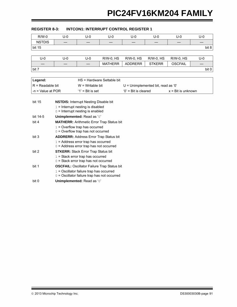
PIC24FV16KM204 FAMILY
REGISTER 8-3: INTCON1: INTERRUPT CONTROL REGISTER 1
R/W-0 U-0 U-0 U-0 U-0 U-0 U-0 U-0
NSTDIS — — — — — — —
bit 15 bit 8
U-0 U-0 U-0 R/W-0, HS R/W-0, HS R/W-0, HS R/W-0, HS U-0
— — — MATHERR ADDRERR STKERR OSCFAIL —
bit 7 bit 0
Legend: HS = Hardware Settable bit
R = Readable bit W = Writable bit U = Unimplemented bit, read as ‘0’
-n = Value at POR ‘1’ = Bit is set ‘0’ = Bit is cleared x = Bit is unknown
bit 15 NSTDIS: Interrupt Nesting Disable bit
1 = Interrupt nesting is disabled0 = Interrupt nesting is enabled
bit 14-5 Unimplemented: Read as ‘0’
bit 4 MATHERR: Arithmetic Error Trap Status bit
1 = Overflow trap has occurred0 = Overflow trap has not occurred
bit 3 ADDRERR: Address Error Trap Status bit
1 = Address error trap has occurred0 = Address error trap has not occurred
bit 2 STKERR: Stack Error Trap Status bit
1 = Stack error trap has occurred0 = Stack error trap has not occurred
bit 1 OSCFAIL: Oscillator Failure Trap Status bit
1 = Oscillator failure trap has occurred0 = Oscillator failure trap has not occurred
bit 0 Unimplemented: Read as ‘0’
2013 Microchip Technology Inc. DS30003030B-page 91
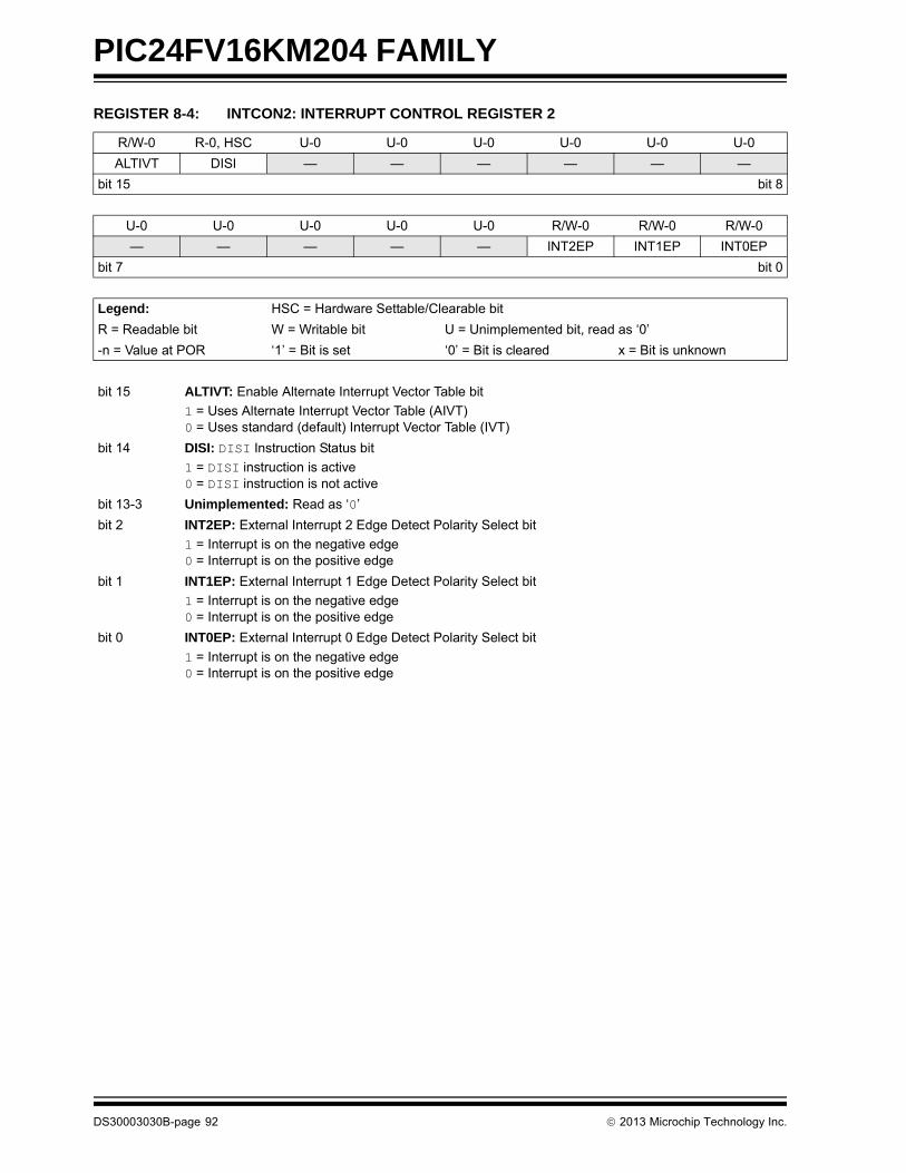
PIC24FV16KM204 FAMILY
REGISTER 8-4: INTCON2: INTERRUPT CONTROL REGISTER 2
R/W-0 R-0, HSC U-0 U-0 U-0 U-0 U-0 U-0
ALTIVT DISI — — — — — —
bit 15 bit 8
U-0 U-0 U-0 U-0 U-0 R/W-0 R/W-0 R/W-0
— — — — — INT2EP INT1EP INT0EP
bit 7 bit 0
Legend: HSC = Hardware Settable/Clearable bit
R = Readable bit W = Writable bit U = Unimplemented bit, read as ‘0’
-n = Value at POR ‘1’ = Bit is set ‘0’ = Bit is cleared x = Bit is unknown
bit 15 ALTIVT: Enable Alternate Interrupt Vector Table bit
1 = Uses Alternate Interrupt Vector Table (AIVT)0 = Uses standard (default) Interrupt Vector Table (IVT)
bit 14 DISI: DISI Instruction Status bit
1 = DISI instruction is active0 = DISI instruction is not active
bit 13-3 Unimplemented: Read as ‘0’
bit 2 INT2EP: External Interrupt 2 Edge Detect Polarity Select bit
1 = Interrupt is on the negative edge 0 = Interrupt is on the positive edge
bit 1 INT1EP: External Interrupt 1 Edge Detect Polarity Select bit
1 = Interrupt is on the negative edge 0 = Interrupt is on the positive edge
bit 0 INT0EP: External Interrupt 0 Edge Detect Polarity Select bit
1 = Interrupt is on the negative edge 0 = Interrupt is on the positive edge
DS30003030B-page 92 2013 Microchip Technology Inc.
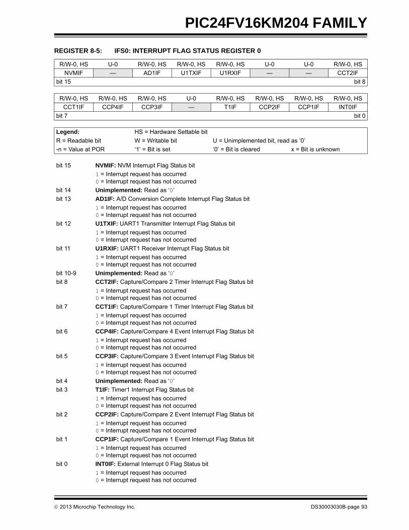
PIC24FV16KM204 FAMILY
REGISTER 8-5: IFS0: INTERRUPT FLAG STATUS REGISTER 0
R/W-0, HS U-0 R/W-0, HS R/W-0, HS R/W-0, HS U-0 U-0 R/W-0, HS
NVMIF — AD1IF U1TXIF U1RXIF — — CCT2IF
bit 15 bit 8
R/W-0, HS R/W-0, HS R/W-0, HS U-0 R/W-0, HS R/W-0, HS R/W-0, HS R/W-0, HS
CCT1IF CCP4IF CCP3IF — T1IF CCP2IF CCP1IF INT0IF
bit 7 bit 0
Legend: HS = Hardware Settable bit
R = Readable bit W = Writable bit U = Unimplemented bit, read as ‘0’
-n = Value at POR ‘1’ = Bit is set ‘0’ = Bit is cleared x = Bit is unknown
bit 15 NVMIF: NVM Interrupt Flag Status bit
1 = Interrupt request has occurred0 = Interrupt request has not occurred
bit 14 Unimplemented: Read as ‘0’
bit 13 AD1IF: A/D Conversion Complete Interrupt Flag Status bit
1 = Interrupt request has occurred0 = Interrupt request has not occurred
bit 12 U1TXIF: UART1 Transmitter Interrupt Flag Status bit
1 = Interrupt request has occurred0 = Interrupt request has not occurred
bit 11 U1RXIF: UART1 Receiver Interrupt Flag Status bit
1 = Interrupt request has occurred0 = Interrupt request has not occurred
bit 10-9 Unimplemented: Read as ‘0’
bit 8 CCT2IF: Capture/Compare 2 Timer Interrupt Flag Status bit
1 = Interrupt request has occurred0 = Interrupt request has not occurred
bit 7 CCT1IF: Capture/Compare 1 Timer Interrupt Flag Status bit
1 = Interrupt request has occurred0 = Interrupt request has not occurred
bit 6 CCP4IF: Capture/Compare 4 Event Interrupt Flag Status bit
1 = Interrupt request has occurred0 = Interrupt request has not occurred
bit 5 CCP3IF: Capture/Compare 3 Event Interrupt Flag Status bit
1 = Interrupt request has occurred0 = Interrupt request has not occurred
bit 4 Unimplemented: Read as ‘0’
bit 3 T1IF: Timer1 Interrupt Flag Status bit
1 = Interrupt request has occurred0 = Interrupt request has not occurred
bit 2 CCP2IF: Capture/Compare 2 Event Interrupt Flag Status bit
1 = Interrupt request has occurred0 = Interrupt request has not occurred
bit 1 CCP1IF: Capture/Compare 1 Event Interrupt Flag Status bit
1 = Interrupt request has occurred0 = Interrupt request has not occurred
bit 0 INT0IF: External Interrupt 0 Flag Status bit
1 = Interrupt request has occurred0 = Interrupt request has not occurred
2013 Microchip Technology Inc. DS30003030B-page 93

PIC24FV16KM204 FAMILY
REGISTER 8-6: IFS1: INTERRUPT FLAG STATUS REGISTER 1
R/W-0, HS R/W-0, HS R/W-0, HS R/W-0, HS R/W-0, HS U-0 U-0 U-0
U2TXIF U2RXIF INT2IF CCT4IF CCT3IF — — —
bit 15 bit 8
U-0 R/W-0, HS U-0 R/W-0, HS R/W-0, HS R/W-0, HS R/W-0, HS R/W-0, HS
— CCP5IF — INT1IF CNIF CMIF BCL1IF SSP1IF
bit 7 bit 0
Legend: HS = Hardware Settable bit
R = Readable bit W = Writable bit U = Unimplemented bit, read as ‘0’
-n = Value at POR ‘1’ = Bit is set ‘0’ = Bit is cleared x = Bit is unknown
bit 15 U2TXIF: UART2 Transmitter Interrupt Flag Status bit
1 = Interrupt request has occurred0 = Interrupt request has not occurred
bit 14 U2RXIF: UART2 Receiver Interrupt Flag Status bit
1 = Interrupt request has occurred0 = Interrupt request has not occurred
bit 13 INT2IF: External Interrupt 2 Flag Status bit
1 = Interrupt request has occurred0 = Interrupt request has not occurred
bit 12 CCT4IF: Capture/Compare 4 Timer Interrupt Flag Status bit
1 = Interrupt request has occurred0 = Interrupt request has not occurred
bit 11 CCT3IF: Capture/Compare 3 Timer Interrupt Flag Status bit
1 = Interrupt request has occurred0 = Interrupt request has not occurred
bit 10-7 Unimplemented: Read as ‘0’
bit 6 CCP5IF: Capture/Compare 5 Event Interrupt Flag Status bit
1 = Interrupt request has occurred0 = Interrupt request has not occurred
bit 5 Unimplemented: Read as ‘0’
bit 4 INT1IF: External Interrupt 1 Flag Status bit
1 = Interrupt request has occurred0 = Interrupt request has not occurred
bit 3 CNIF: Input Change Notification Interrupt Flag Status bit
1 = Interrupt request has occurred0 = Interrupt request has not occurred
bit 2 CMIF: Comparator Interrupt Flag Status Bit
1 = Interrupt request has occurred0 = Interrupt request has not occurred
bit 1 BCL1IF: MSSP1 I2C™ Bus Collision Interrupt Flag Status bit
1 = Interrupt request has occurred0 = Interrupt request has not occurred
bit 0 SI2C1IF: MSSP1 SPI/I2C Event Interrupt Flag Status bit
1 = Interrupt request has occurred0 = Interrupt request has not occurred
DS30003030B-page 94 2013 Microchip Technology Inc.

PIC24FV16KM204 FAMILY
REGISTER 8-7: IFS2: INTERRUPT FLAG STATUS REGISTER 2
U-0 U-0 U-0 U-0 U-0 U-0 R/W-0, HS U-0
— — — — — — CCT5IF —
bit 15 bit 8
U-0 U-0 U-0 U-0 U-0 U-0 U-0 U-0
— — — — — — — —
bit 7 bit 0
Legend: HS = Hardware Settable bit
R = Readable bit W = Writable bit U = Unimplemented bit, read as ‘0’
-n = Value at POR ‘1’ = Bit is set ‘0’ = Bit is cleared x = Bit is unknown
bit 15-10 Unimplemented: Read as ‘0’
bit 9 CCT5IF: Capture/Compare 5 Timer Interrupt Flag Status bit
1 = Interrupt request has occurred0 = Interrupt request has not occurred
bit 8-0 Unimplemented: Read as ‘0’
REGISTER 8-8: IFS3: INTERRUPT FLAG STATUS REGISTER 3
U-0 R/W-0, HS U-0 U-0 U-0 U-0 U-0 U-0
— RTCIF — — — — — —
bit 15 bit 8
U-0 U-0 U-0 U-0 U-0 R/W-0, HS R/W-0, HS U-0
— — — — — BCL2IF SSP2IF —
bit 7 bit 0
Legend: HS = Hardware Settable bit
R = Readable bit W = Writable bit U = Unimplemented bit, read as ‘0’
-n = Value at POR ‘1’ = Bit is set ‘0’ = Bit is cleared x = Bit is unknown
bit 15 Unimplemented: Read as ‘0’
bit 14 RTCIF: Real-Time Clock and Calendar Interrupt Flag Status bit
1 = Interrupt request has occurred0 = Interrupt request has not occurred
bit 13-3 Unimplemented: Read as ‘0’
bit 2 BCL2IF: MSSP2 I2C™ Bus Collision Interrupt Flag Status bit
1 = Interrupt request has occurred0 = Interrupt request has not occurred
bit 1 SSP2IF: MSSP2 SPI/I2C Event Interrupt Flag Status bit
1 = Interrupt request has occurred0 = Interrupt request has not occurred
bit 0 Unimplemented: Read as ‘0’
2013 Microchip Technology Inc. DS30003030B-page 95

PIC24FV16KM204 FAMILY
REGISTER 8-9: IFS4: INTERRUPT FLAG STATUS REGISTER 4
R/W-0, HS R/W-0, HS R/W-0, HS U-0 U-0 U-0 U-0 R/W-0, HS
DAC2IF DAC1IF CTMUIF — — — — HLVDIF
bit 15 bit 8
U-0 U-0 U-0 U-0 U-0 R/W-0, HS R/W-0, HS U-0
— — — — — U2ERIF U1ERIF —
bit 7 bit 0
Legend: HS = Hardware Settable bit
R = Readable bit W = Writable bit U = Unimplemented bit, read as ‘0’
-n = Value at POR ‘1’ = Bit is set ‘0’ = Bit is cleared x = Bit is unknown
bit 15 DAC2IF: Digital-to-Analog Converter 2 Interrupt Flag Status bit
1 = Interrupt request has occurred0 = Interrupt request has not occurred
bit 14 DAC1IF: Digital-to-Analog Converter 1 Interrupt Flag Status bit
1 = Interrupt request has occurred0 = Interrupt request has not occurred
bit 13 CTMUIF: CTMU Interrupt Flag Status bit
1 = Interrupt request has occurred0 = Interrupt request has not occurred
bit 12-9 Unimplemented: Read as ‘0’
bit 8 HLVDIF: High/Low-Voltage Detect Interrupt Flag Status bit
1 = Interrupt request has occurred0 = Interrupt request has not occurred
bit 7-3 Unimplemented: Read as ‘0’
bit 2 U2ERIF: UART2 Error Interrupt Flag Status bit
1 = Interrupt request has occurred0 = Interrupt request has not occurred
bit 1 U1ERIF: UART1 Error Interrupt Flag Status bit
1 = Interrupt request has occurred0 = Interrupt request has not occurred
bit 0 Unimplemented: Read as ‘0’
DS30003030B-page 96 2013 Microchip Technology Inc.

PIC24FV16KM204 FAMILY
2013 Microchip Technology Inc. DS30003030B-page 97
REGISTER 8-10: IFS5: INTERRUPT FLAG STATUS REGISTER 5
U-0 U-0 U-0 U-0 U-0 U-0 U-0 U-0
— — — — — — — —
bit 15 bit 8
U-0 U-0 U-0 U-0 U-0 U-0 U-0 R/W-0, HS
— — — — — — — ULPWUIF
bit 7 bit 0
Legend: HS = Hardware Settable bit
R = Readable bit W = Writable bit U = Unimplemented bit, read as ‘0’
-n = Value at POR ‘1’ = Bit is set ‘0’ = Bit is cleared x = Bit is unknown
bit 15-1 Unimplemented: Read as ‘0’
bit 0 ULPWUIF: Ultra Low-Power Wake-up Interrupt Flag Status bit
1 = Interrupt request has occurred0 = Interrupt request has not occurred
REGISTER 8-11: IFS6: INTERRUPT FLAG STATUS REGISTER 6
U-0 U-0 U-0 U-0 U-0 U-0 U-0 U-0
— — — — — — — —
bit 15 bit 8
U-0 U-0 U-0 U-0 U-0 U-0 R/W-0, HS R/W-0, HS
— — — — — — CLC2IF CLC1IF
bit 7 bit 0
Legend: HS = Hardware Settable bit
R = Readable bit W = Writable bit U = Unimplemented bit, read as ‘0’
-n = Value at POR ‘1’ = Bit is set ‘0’ = Bit is cleared x = Bit is unknown
bit 15-2 Unimplemented: Read as ‘0’
bit 1 CLC2IF: Configurable Logic Cell 2 Interrupt Flag Status bit
1 = Interrupt request has occurred0 = Interrupt request has not occurred
bit 0 CLC1IF: Configurable Logic Cell 1 Interrupt Flag Status bit
1 = Interrupt request has occurred0 = Interrupt request has not occurred

PIC24FV16KM204 FAMILY
REGISTER 8-12: IEC0: INTERRUPT ENABLE CONTROL REGISTER 0
R/W-0 U-0 R/W-0 R/W-0 R/W-0 U-0 U-0 R/W-0
NVMIE — AD1IE U1TXIE U1RXIE — — CCT2IE
bit 15 bit 8
R/W-0 R/W-0 R/W-0 U-0 R/W-0 R/W-0 R/W-0 R/W-0
CCT1IE CCP4IE CCP3IE — T1IE CCP2IE CCP1IE INT0IE
bit 7 bit 0
Legend:
R = Readable bit W = Writable bit U = Unimplemented bit, read as ‘0’
-n = Value at POR ‘1’ = Bit is set ‘0’ = Bit is cleared x = Bit is unknown
bit 15 NVMIE: NVM Interrupt Enable bit
1 = Interrupt request is enabled0 = Interrupt request is not enabled
bit 14 Unimplemented: Read as ‘0’
bit 13 AD1IE: A/D Conversion Complete Interrupt Enable bit
1 = Interrupt request is enabled0 = Interrupt request is not enabled
bit 12 U1TXIE: UART1 Transmitter Interrupt Enable bit
1 = Interrupt request is enabled0 = Interrupt request is not enabled
bit 11 U1RXIE: UART1 Receiver Interrupt Enable bit
1 = Interrupt request is enabled0 = Interrupt request is not enabled
bit 10-9 Unimplemented: Read as ‘0’
bit 8 CCT2IE: Capture/Compare 2 Timer Interrupt Enable bit
1 = Interrupt request is enabled0 = Interrupt request is not enabled
bit 7 CCT1IE: Capture/Compare 1 Timer Interrupt Enable bit
1 = Interrupt request is enabled0 = Interrupt request is not enabled
bit 6 CCP4IE: Capture/Compare 4 Event Interrupt Enable bit1 = Interrupt request is enabled0 = Interrupt request is not enabled
bit 5 CCP3IE: Capture/Compare 3 Event Interrupt Enable bit
1 = Interrupt request is enabled0 = Interrupt request is not enabled
bit 4 Unimplemented: Read as ‘0’
bit 3 T1IE: Timer1 Interrupt Enable bit
1 = Interrupt request is enabled0 = Interrupt request is not enabled
bit 2 CCP2IE: Capture/Compare 2 Event Interrupt Enable bit
1 = Interrupt request is enabled0 = Interrupt request is not enabled
bit 1 CCP1IE: Capture/Compare 1 Event Interrupt Enable bit
1 = Interrupt request is enabled0 = Interrupt request is not enabled
bit 0 INT0IE: External Interrupt 0 Enable bit
1 = Interrupt request is enabled0 = Interrupt request is not enabled
DS30003030B-page 98 2013 Microchip Technology Inc.

PIC24FV16KM204 FAMILY
REGISTER 8-13: IEC1: INTERRUPT ENABLE CONTROL REGISTER 1
R/W-0 R/W-0 R/W-0 R/W-0 R/W-0 U-0 U-0 U-0
U2TXIE U2RXIE INT2IE CCT4IE CCT3IE — — —
bit 15 bit 8
U-0 R/W-0 U-0 R/W-0 R/W-0 R/W-0 R/W-0 R/W-0
— CCP5IE — INT1IE CNIE CMIE BCL1IE SSP1IE
bit 7 bit 0
Legend:
R = Readable bit W = Writable bit U = Unimplemented bit, read as ‘0’
-n = Value at POR ‘1’ = Bit is set ‘0’ = Bit is cleared x = Bit is unknown
bit 15 U2TXIE: UART2 Transmitter Interrupt Enable bit
1 = Interrupt request is enabled0 = Interrupt request is not enabled
bit 14 U2RXIE: UART2 Receiver Interrupt Enable bit
1 = Interrupt request is enabled0 = Interrupt request is not enabled
bit 13 INT2IE: External Interrupt 2 Enable bit
1 = Interrupt request is enabled0 = Interrupt request is not enabled
bit 12 CCT4IE: Capture/Compare 4 Timer Interrupt Enable bit
1 = Interrupt request is enabled0 = Interrupt request is not enabled
bit 11 CCT3IE: Capture/Compare 3 Timer Interrupt Enable bit
1 = Interrupt request is enabled0 = Interrupt request is not enabled
bit 10-7 Unimplemented: Read as ‘0’
bit 6 CCP5IE: Capture/Compare 5 Event Interrupt Enable bit
1 = Interrupt request is enabled0 = Interrupt request is not enabled
bit 5 Unimplemented: Read as ‘0’
bit 4 INT1IE: External Interrupt 1 Enable bit
1 = Interrupt request is enabled0 = Interrupt request is not enabled
bit 3 CNIE: Input Change Notification Interrupt Enable bit
1 = Interrupt request is enabled0 = Interrupt request is not enabled
bit 2 CMIE: Comparator Interrupt Enable bit
1 = Interrupt request is enabled0 = Interrupt request is not enabled
bit 1 BCL1IE: MSSP1 I2C™ Bus Collision Interrupt Enable bit
1 = Interrupt request is enabled0 = Interrupt request is not enabled
bit 0 SSP1IE: MSSP1 SPI/I2C Event Interrupt Enable bit
1 = Interrupt request is enabled0 = Interrupt request is not enabled
2013 Microchip Technology Inc. DS30003030B-page 99

PIC24FV16KM204 FAMILY
REGISTER 8-14: IEC2: INTERRUPT ENABLE CONTROL REGISTER 2
U-0 U-0 U-0 U-0 U-0 U-0 R/W-0 U-0
— — — — — — CCT5IE —
bit 15 bit 8
U-0 U-0 U-0 U-0 U-0 U-0 U-0 U-0
— — — — — — — —
bit 7 bit 0
Legend:
R = Readable bit W = Writable bit U = Unimplemented bit, read as ‘0’
-n = Value at POR ‘1’ = Bit is set ‘0’ = Bit is cleared x = Bit is unknown
bit 15-10 Unimplemented: Read as ‘0’
bit 9 CCT5IE: Capture/Compare 5 Timer Interrupt Enable bit
1 = Interrupt request is enabled0 = Interrupt request is not enabled
bit 8-0 Unimplemented: Read as ‘0’
REGISTER 8-15: IEC3: INTERRUPT ENABLE CONTROL REGISTER 3
U-0 R/W-0 U-0 U-0 U-0 U-0 U-0 U-0
— RTCIE — — — — — —
bit 15 bit 8
U-0 U-0 U-0 U-0 U-0 R/W-0 R/W-0 U-0
— — — — — BCL2IE SSP2IE —
bit 7 bit 0
Legend:
R = Readable bit W = Writable bit U = Unimplemented bit, read as ‘0’
-n = Value at POR ‘1’ = Bit is set ‘0’ = Bit is cleared x = Bit is unknown
bit 15 Unimplemented: Read as ‘0’
bit 14 RTCIE: Real-Time Clock and Calendar Interrupt Enable bit
1 = Interrupt request is enabled0 = Interrupt request is not enabled
bit 13-3 Unimplemented: Read as ‘0’
bit 2 BCL2IE: MSSP2 I2C™ Bus Collision Interrupt Enable bit
1 = Interrupt request is enabled0 = Interrupt request is not enabled
bit 1 SSP2IE: MSSP2 SPI/I2C Event Interrupt Enable bit
1 = Interrupt request is enabled0 = Interrupt request is not enabled
bit 0 Unimplemented: Read as ‘0’
DS30003030B-page 100 2013 Microchip Technology Inc.

PIC24FV16KM204 FAMILY
REGISTER 8-16: IEC4: INTERRUPT ENABLE CONTROL REGISTER 4
R/W-0 R/W-0 R/W-0 U-0 U-0 U-0 U-0 R/W-0
DAC2IE DAC1IE CTMUIE — — — — HLVDIE
bit 15 bit 8
U-0 U-0 U-0 U-0 U-0 R/W-0 R/W-0 U-0
— — — — — U2ERIE U1ERIE —
bit 7 bit 0
Legend:
R = Readable bit W = Writable bit U = Unimplemented bit, read as ‘0’
-n = Value at POR ‘1’ = Bit is set ‘0’ = Bit is cleared x = Bit is unknown
bit 15 DAC2IE: Digital-to-Analog Converter 2 Interrupt Enable bit
1 = Interrupt request is enabled0 = Interrupt request is not enabled
bit 14 DAC1IE: Digital-to-Analog Converter 1 Interrupt Enable bit
1 = Interrupt request is enabled0 = Interrupt request is not enabled
bit 13 CTMUIE: CTMU Interrupt Enable bit
1 = Interrupt request is enabled0 = Interrupt request is not enabled
bit 12-9 Unimplemented: Read as ‘0’
bit 8 HLVDIE: High/Low-Voltage Detect Interrupt Enable bit
1 = Interrupt request is enabled0 = Interrupt request is not enabled
bit 7-3 Unimplemented: Read as ‘0’
bit 2 U2ERIE: UART2 Error Interrupt Enable bit
1 = Interrupt request is enabled0 = Interrupt request is not enabled
bit 1 U1ERIE: UART1 Error Interrupt Enable bit
1 = Interrupt request is enabled0 = Interrupt request is not enabled
bit 0 Unimplemented: Read as ‘0’
2013 Microchip Technology Inc. DS30003030B-page 101

PIC24FV16KM204 FAMILY
REGISTER 8-17: IEC5: INTERRUPT ENABLE CONTROL REGISTER 5
U-0 U-0 U-0 U-0 U-0 U-0 U-0 U-0
— — — — — — — —
bit 15 bit 8
U-0 U-0 U-0 U-0 U-0 U-0 U-0 R/W-0
— — — — — — — ULPWUIE
bit 7 bit 0
Legend:
R = Readable bit W = Writable bit U = Unimplemented bit, read as ‘0’
-n = Value at POR ‘1’ = Bit is set ‘0’ = Bit is cleared x = Bit is unknown
bit 15-1 Unimplemented: Read as ‘0’
bit 0 ULPWUIE: Ultra Low-Power Wake-up Interrupt Enable bit
1 = Interrupt request is enabled0 = Interrupt request is not enabled
REGISTER 8-18: IEC6: INTERRUPT ENABLE CONTROL REGISTER 5
U-0 U-0 U-0 U-0 U-0 U-0 U-0 U-0
— — — — — — — —
bit 15 bit 8
U-0 U-0 U-0 U-0 U-0 U-0 R/W-0 R/W-0
— — — — — — CLC2IE CLC1IE
bit 7 bit 0
Legend:
R = Readable bit W = Writable bit U = Unimplemented bit, read as ‘0’
-n = Value at POR ‘1’ = Bit is set ‘0’ = Bit is cleared x = Bit is unknown
bit 15-2 Unimplemented: Read as ‘0’
bit 1 CLC2IE: Configurable Logic Cell 2 Interrupt Enable bit
1 = Interrupt request is enabled0 = Interrupt request is not enabled
bit 0 CLC1IE: Configurable Logic Cell 1 Interrupt Enable bit
1 = Interrupt request is enabled0 = Interrupt request is not enabled
DS30003030B-page 102 2013 Microchip Technology Inc.

PIC24FV16KM204 FAMILY
REGISTER 8-19: IPC0: INTERRUPT PRIORITY CONTROL REGISTER 0
U-0 R/W-1 R/W-0 R/W-0 U-0 R/W-1 R/W-0 R/W-0
— T1IP2 T1IP1 T1IP0 — CCP2IP2 CCP2IP1 CCP2IP0
bit 15 bit 8
U-0 R/W-1 R/W-0 R/W-0 U-0 R/W-1 R/W-0 R/W-0
— CCP1IP2 CCP1IP1 CCP1IP0 — INT0IP2 INT0IP1 INT0IP0
bit 7 bit 0
Legend:
R = Readable bit W = Writable bit U = Unimplemented bit, read as ‘0’
-n = Value at POR ‘1’ = Bit is set ‘0’ = Bit is cleared x = Bit is unknown
bit 15 Unimplemented: Read as ‘0’
bit 14-12 T1IP<2:0>: Timer1 Interrupt Priority bits
111 = Interrupt is Priority 7 (highest priority interrupt)•••001 = Interrupt is Priority 1000 = Interrupt source is disabled
bit 11 Unimplemented: Read as ‘0’
bit 10-8 CCP2IP<2:0>: Capture/Compare 2 Event Interrupt Priority bits
111 = Interrupt is Priority 7 (highest priority interrupt)•••001 = Interrupt is Priority 1000 = Interrupt source is disabled
bit 7 Unimplemented: Read as ‘0’
bit 6-4 CCP1IP<2:0>: Capture/Compare 1 Event Interrupt Priority bits
111 = Interrupt is Priority 7 (highest priority interrupt)•••001 = Interrupt is Priority 1000 = Interrupt source is disabled
bit 3 Unimplemented: Read as ‘0’
bit 2-0 INT0IP<2:0>: External Interrupt 0 Interrupt Priority bits
111 = Interrupt is Priority 7 (highest priority interrupt)•••001 = Interrupt is Priority 1000 = Interrupt source is disabled
2013 Microchip Technology Inc. DS30003030B-page 103
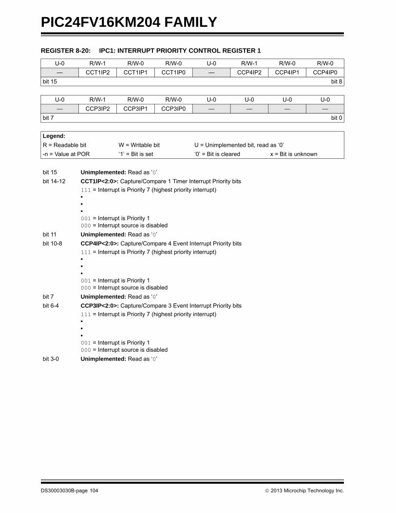
PIC24FV16KM204 FAMILY
REGISTER 8-20: IPC1: INTERRUPT PRIORITY CONTROL REGISTER 1
U-0 R/W-1 R/W-0 R/W-0 U-0 R/W-1 R/W-0 R/W-0
— CCT1IP2 CCT1IP1 CCT1IP0 — CCP4IP2 CCP4IP1 CCP4IP0
bit 15 bit 8
U-0 R/W-1 R/W-0 R/W-0 U-0 U-0 U-0 U-0
— CCP3IP2 CCP3IP1 CCP3IP0 — — — —
bit 7 bit 0
Legend:
R = Readable bit W = Writable bit U = Unimplemented bit, read as ‘0’
-n = Value at POR ‘1’ = Bit is set ‘0’ = Bit is cleared x = Bit is unknown
bit 15 Unimplemented: Read as ‘0’
bit 14-12 CCT1IP<2:0>: Capture/Compare 1 Timer Interrupt Priority bits
111 = Interrupt is Priority 7 (highest priority interrupt)•••001 = Interrupt is Priority 1000 = Interrupt source is disabled
bit 11 Unimplemented: Read as ‘0’
bit 10-8 CCP4IP<2:0>: Capture/Compare 4 Event Interrupt Priority bits
111 = Interrupt is Priority 7 (highest priority interrupt)•••001 = Interrupt is Priority 1000 = Interrupt source is disabled
bit 7 Unimplemented: Read as ‘0’
bit 6-4 CCP3IP<2:0>: Capture/Compare 3 Event Interrupt Priority bits
111 = Interrupt is Priority 7 (highest priority interrupt)•••001 = Interrupt is Priority 1000 = Interrupt source is disabled
bit 3-0 Unimplemented: Read as ‘0’
DS30003030B-page 104 2013 Microchip Technology Inc.
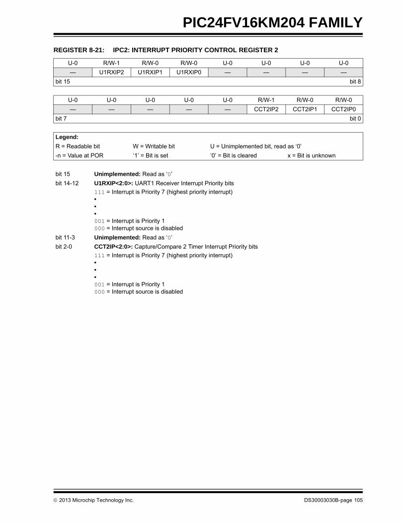
PIC24FV16KM204 FAMILY
REGISTER 8-21: IPC2: INTERRUPT PRIORITY CONTROL REGISTER 2
U-0 R/W-1 R/W-0 R/W-0 U-0 U-0 U-0 U-0
— U1RXIP2 U1RXIP1 U1RXIP0 — — — —
bit 15 bit 8
U-0 U-0 U-0 U-0 U-0 R/W-1 R/W-0 R/W-0
— — — — — CCT2IP2 CCT2IP1 CCT2IP0
bit 7 bit 0
Legend:
R = Readable bit W = Writable bit U = Unimplemented bit, read as ‘0’
-n = Value at POR ‘1’ = Bit is set ‘0’ = Bit is cleared x = Bit is unknown
bit 15 Unimplemented: Read as ‘0’
bit 14-12 U1RXIP<2:0>: UART1 Receiver Interrupt Priority bits
111 = Interrupt is Priority 7 (highest priority interrupt)•••001 = Interrupt is Priority 1000 = Interrupt source is disabled
bit 11-3 Unimplemented: Read as ‘0’
bit 2-0 CCT2IP<2:0>: Capture/Compare 2 Timer Interrupt Priority bits
111 = Interrupt is Priority 7 (highest priority interrupt)•••001 = Interrupt is Priority 1000 = Interrupt source is disabled
2013 Microchip Technology Inc. DS30003030B-page 105

PIC24FV16KM204 FAMILY
REGISTER 8-22: IPC3: INTERRUPT PRIORITY CONTROL REGISTER 3
U-0 R/W-1 R/W-0 R/W-0 U-0 U-0 U-0 U-0
— NVMIP2 NVMIP1 NVMIP0 — — — —
bit 15 bit 8
U-0 R/W-1 R/W-0 R/W-0 U-0 R/W-1 R/W-0 R/W-0
— AD1IP2 AD1IP1 AD1IP0 — U1TXIP2 U1TXIP1 U1TXIP0
bit 7 bit 0
Legend:
R = Readable bit W = Writable bit U = Unimplemented bit, read as ‘0’
-n = Value at POR ‘1’ = Bit is set ‘0’ = Bit is cleared x = Bit is unknown
bit 15 Unimplemented: Read as ‘0’
bit 14-12 NVMIP<2:0>: NVM Interrupt Priority bits111 = Interrupt is Priority 7 (highest priority interrupt)•••001 = Interrupt is Priority 1000 = Interrupt source is disabled
bit 11-7 Unimplemented: Read as ‘0’
bit 6-4 AD1IP<2:0>: A/D Conversion Complete Interrupt Priority bits
111 = Interrupt is Priority 7 (highest priority interrupt)•••001 = Interrupt is Priority 1000 = Interrupt source is disabled
bit 3 Unimplemented: Read as ‘0’
bit 2-0 U1TXIP<2:0>: UART1 Transmitter Interrupt Priority bits
111 = Interrupt is Priority 7 (highest priority interrupt)•••001 = Interrupt is Priority 1000 = Interrupt source is disabled
DS30003030B-page 106 2013 Microchip Technology Inc.

PIC24FV16KM204 FAMILY
REGISTER 8-23: IPC4: INTERRUPT PRIORITY CONTROL REGISTER 4
U-0 R/W-1 R/W-0 R/W-0 U-0 R/W-1 R/W-0 R/W-0
— CNIP2 CNIP1 CNIP0 — CMIP2 CMIP1 CMIP0
bit 15 bit 8
U-0 R/W-1 R/W-0 R/W-0 U-0 R/W-1 R/W-0 R/W-0
— BCL1IP2 BCL1IP1 BCL1IP0 — SSP1IP2 SSP1IP1 SSP1IP0
bit 7 bit 0
Legend:
R = Readable bit W = Writable bit U = Unimplemented bit, read as ‘0’
-n = Value at POR ‘1’ = Bit is set ‘0’ = Bit is cleared x = Bit is unknown
bit 15 Unimplemented: Read as ‘0’
bit 14-12 CNIP<2:0>: Input Change Notification Interrupt Priority bits
111 = Interrupt is Priority 7 (highest priority interrupt)•••001 = Interrupt is Priority 1000 = Interrupt source is disabled
bit 11 Unimplemented: Read as ‘0’
bit 10-8 CMIP<2:0>: Comparator Interrupt Priority bits
111 = Interrupt is Priority 7 (highest priority interrupt)•••001 = Interrupt is Priority 1000 = Interrupt source is disabled
bit 7 Unimplemented: Read as ‘0’
bit 6-4 BCL1IP<2:0>: MSSP1 I2C™ Bus Collision Interrupt Priority bits
111 = Interrupt is Priority 7 (highest priority interrupt)•••001 = Interrupt is Priority 1000 = Interrupt source is disabled
bit 3 Unimplemented: Read as ‘0’
bit 2-0 SSP1IP<2:0>: MSSP1 SPI/I2C Event Interrupt Priority bits
111 = Interrupt is Priority 7 (highest priority interrupt)•••001 = Interrupt is Priority 1000 = Interrupt source is disabled
2013 Microchip Technology Inc. DS30003030B-page 107

PIC24FV16KM204 FAMILY
REGISTER 8-24: IPC5: INTERRUPT PRIORITY CONTROL REGISTER 5
U-0 U-0 U-0 U-0 U-0 R/W-1 R/W-0 R/W-0
— — — — — CCP5IP2 CCP5IP1 CCP5IP0
bit 15 bit 8
U-0 U-0 U-0 U-0 U-0 R/W-1 R/W-0 R/W-0
— — — — — INT1IP2 INT1IP1 INT1IP0
bit 7 bit 0
Legend:
R = Readable bit W = Writable bit U = Unimplemented bit, read as ‘0’
-n = Value at POR ‘1’ = Bit is set ‘0’ = Bit is cleared x = Bit is unknown
bit 15-11 Unimplemented: Read as ‘0’
bit 10-8 CCP5IP<2:0>: Capture/Compare 5 Event Interrupt Priority bits
111 = Interrupt is Priority 7 (highest priority interrupt)•••001 = Interrupt is Priority 1000 = Interrupt source is disabled
bit 7-3 Unimplemented: Read as ‘0’
bit 2-0 INT1IP<2:0>: External Interrupt 1 Priority bits
111 = Interrupt is Priority 7 (highest priority interrupt)•••001 = Interrupt is Priority 1000 = Interrupt source is disabled
DS30003030B-page 108 2013 Microchip Technology Inc.

PIC24FV16KM204 FAMILY
REGISTER 8-25: IPC6: INTERRUPT PRIORITY CONTROL REGISTER 6
U-0 R/W-1 R/W-0 R/W-0 U-0 U-0 U-0 U-0
— CCT3IP2 CCT3IP1 CCT3IP0 — — — —
bit 15 bit 8
U-0 U-0 U-0 U-0 U-0 U-0 U-0 U-0
— — — — — — — —
bit 7 bit 0
Legend:
R = Readable bit W = Writable bit U = Unimplemented bit, read as ‘0’
-n = Value at POR ‘1’ = Bit is set ‘0’ = Bit is cleared x = Bit is unknown
bit 15 Unimplemented: Read as ‘0’
bit 14-12 CCT3IP<2:0>: Capture/Compare 3 Timer Interrupt Priority bits
111 = Interrupt is Priority 7 (highest priority interrupt)•••001 = Interrupt is Priority 1000 = Interrupt source is disabled
bit 11-0 Unimplemented: Read as ‘0’
2013 Microchip Technology Inc. DS30003030B-page 109

PIC24FV16KM204 FAMILY
REGISTER 8-26: IPC7: INTERRUPT PRIORITY CONTROL REGISTER 7
U-0 R/W-1 R/W-0 R/W-0 U-0 R/W-1 R/W-0 R/W-0
— U2TXIP2 U2TXIP1 U2TXIP0 — U2RXIP2 U2RXIP1 U2RXIP0
bit 15 bit 8
U-0 R/W-1 R/W-0 R/W-0 U-0 R/W-1 R/W-0 R/W-0
— INT2IP2 INT2IP1 INT2IP0 — CCT4IP2 CCT4IP1 CCT4IP0
bit 7 bit 0
Legend:
R = Readable bit W = Writable bit U = Unimplemented bit, read as ‘0’
-n = Value at POR ‘1’ = Bit is set ‘0’ = Bit is cleared x = Bit is unknown
bit 15 Unimplemented: Read as ‘0’
bit 14-12 U2TXIP<2:0>: UART2 Transmitter Interrupt Priority bits
111 = Interrupt is Priority 7 (highest priority interrupt)•••001 = Interrupt is Priority 1000 = Interrupt source is disabled
bit 11 Unimplemented: Read as ‘0’
bit 10-8 U2RXIP<2:0>: UART2 Receiver Interrupt Priority bits
111 = Interrupt is Priority 7 (highest priority interrupt)•••001 = Interrupt is Priority 1000 = Interrupt source is disabled
bit 7 Unimplemented: Read as ‘0’
bit 6-4 INT2IP<2:0>: External Interrupt 2 Priority bits
111 = Interrupt is Priority 7 (highest priority interrupt)•••001 = Interrupt is Priority 1000 = Interrupt source is disabled
bit 3 Unimplemented: Read as ‘0’
bit 2-0 CCT4IP<2:0>: Capture/Compare 4 Timer Interrupt Priority bits
111 = Interrupt is Priority 7 (highest priority interrupt)•••001 = Interrupt is Priority 1000 = Interrupt source is disabled
DS30003030B-page 110 2013 Microchip Technology Inc.

PIC24FV16KM204 FAMILY
REGISTER 8-27: IPC10: INTERRUPT PRIORITY CONTROL REGISTER 10
U-0 U-0 U-0 U-0 U-0 U-0 U-0 U-0
— — — — — — — —
bit 15 bit 8
U-0 R/W-1 R/W-0 R/W-0 U-0 U-0 U-0 U-0
— CCT5IP2 CCT5IP1 CCT5IP0 — — — —
bit 7 bit 0
Legend:
R = Readable bit W = Writable bit U = Unimplemented bit, read as ‘0’
-n = Value at POR ‘1’ = Bit is set ‘0’ = Bit is cleared x = Bit is unknown
bit 15-7 Unimplemented: Read as ‘0’
bit 6-4 CCT5IP<2:0>: Capture/Compare 5 Timer Interrupt Priority bits
111 = Interrupt is Priority 7 (highest priority interrupt)•••001 = Interrupt is Priority 1000 = Interrupt source is disabled
bit 3-0 Unimplemented: Read as ‘0’
2013 Microchip Technology Inc. DS30003030B-page 111

PIC24FV16KM204 FAMILY
REGISTER 8-28: IPC12: INTERRUPT PRIORITY CONTROL REGISTER 12
U-0 U-0 U-0 U-0 U-0 R/W-1 R/W-0 R/W-0
— — — — — BCL2IP2 BCL2IP1 BCL2IP0
bit 15 bit 8
U-0 R/W-1 R/W-0 R/W-0 U-0 U-0 U-0 U-0
— SSP2IP2 SSP2IP1 SSP2IP0 — — — —
bit 7 bit 0
Legend:
R = Readable bit W = Writable bit U = Unimplemented bit, read as ‘0’
-n = Value at POR ‘1’ = Bit is set ‘0’ = Bit is cleared x = Bit is unknown
bit 15-11 Unimplemented: Read as ‘0’
bit 10-8 BCL2IP<2:0>: MSSP2 I2C™ Bus Collision Interrupt Priority bits
111 = Interrupt is Priority 7 (highest priority interrupt)•••001 = Interrupt is Priority 1000 = Interrupt source is disabled
bit 7 Unimplemented: Read as ‘0’
bit 6-4 SSP2IP<2:0>: MSSP2 SPI/I2C Event Interrupt Priority bits
111 = Interrupt is Priority 7 (highest priority interrupt)•••001 = Interrupt is Priority 1000 = Interrupt source is disabled
bit 3-0 Unimplemented: Read as ‘0’
DS30003030B-page 112 2013 Microchip Technology Inc.

PIC24FV16KM204 FAMILY
REGISTER 8-29: IPC15: INTERRUPT PRIORITY CONTROL REGISTER 15
U-0 U-0 U-0 U-0 U-0 R/W-1 R/W-0 R/W-0
— — — — — RTCIP2 RTCIP1 RTCIP0
bit 15 bit 8
U-0 U-0 U-0 U-0 U-0 U-0 U-0 U-0
— — — — — — — —
bit 7 bit 0
Legend:
R = Readable bit W = Writable bit U = Unimplemented bit, read as ‘0’
-n = Value at POR ‘1’ = Bit is set ‘0’ = Bit is cleared x = Bit is unknown
bit 15-11 Unimplemented: Read as ‘0’
bit 10-8 RTCIP<2:0>: Real-Time Clock and Calendar Interrupt Priority bits
111 = Interrupt is Priority 7 (highest priority interrupt)•••001 = Interrupt is Priority 1000 = Interrupt source is disabled
bit 7-0 Unimplemented: Read as ‘0’
2013 Microchip Technology Inc. DS30003030B-page 113

PIC24FV16KM204 FAMILY
REGISTER 8-30: IPC16: INTERRUPT PRIORITY CONTROL REGISTER 16
U-0 U-0 U-0 U-0 U-0 R/W-1 R/W-0 R/W-0
— — — — — U2ERIP2 U2ERIP1 U2ERIP0
bit 15 bit 8
U-0 R/W-1 R/W-0 R/W-0 U-0 U-0 U-0 U-0
— U1ERIP2 U1ERIP1 U1ERIP0 — — — —
bit 7 bit 0
Legend:
R = Readable bit W = Writable bit U = Unimplemented bit, read as ‘0’
-n = Value at POR ‘1’ = Bit is set ‘0’ = Bit is cleared x = Bit is unknown
bit 15-11 Unimplemented: Read as ‘0’
bit 10-8 U2ERIP<2:0>: UART2 Error Interrupt Priority bits
111 = Interrupt is Priority 7 (highest priority interrupt)•••001 = Interrupt is Priority 1000 = Interrupt source is disabled
bit 7 Unimplemented: Read as ‘0’
bit 6-4 U1ERIP<2:0>: UART1 Error Interrupt Priority bits
111 = Interrupt is Priority 7 (highest priority interrupt)•••001 = Interrupt is Priority 1000 = Interrupt source is disabled
bit 3-0 Unimplemented: Read as ‘0’
DS30003030B-page 114 2013 Microchip Technology Inc.
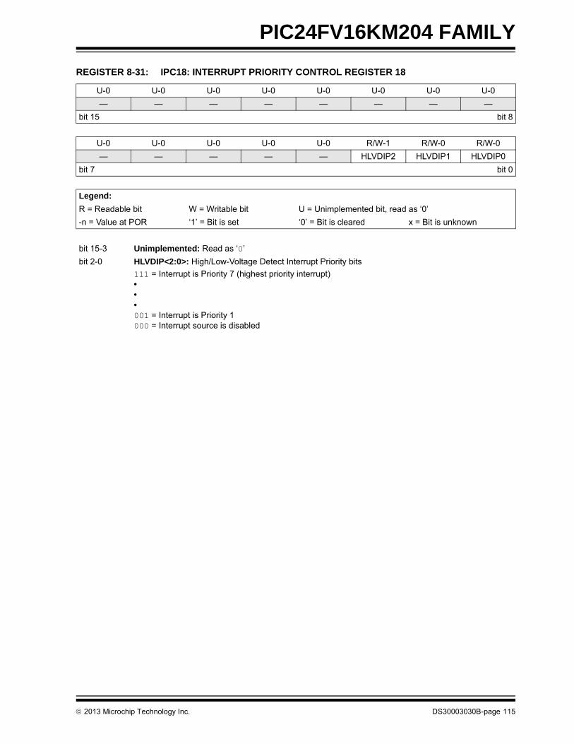
PIC24FV16KM204 FAMILY
REGISTER 8-31: IPC18: INTERRUPT PRIORITY CONTROL REGISTER 18
U-0 U-0 U-0 U-0 U-0 U-0 U-0 U-0
— — — — — — — —
bit 15 bit 8
U-0 U-0 U-0 U-0 U-0 R/W-1 R/W-0 R/W-0
— — — — — HLVDIP2 HLVDIP1 HLVDIP0
bit 7 bit 0
Legend:
R = Readable bit W = Writable bit U = Unimplemented bit, read as ‘0’
-n = Value at POR ‘1’ = Bit is set ‘0’ = Bit is cleared x = Bit is unknown
bit 15-3 Unimplemented: Read as ‘0’
bit 2-0 HLVDIP<2:0>: High/Low-Voltage Detect Interrupt Priority bits
111 = Interrupt is Priority 7 (highest priority interrupt)•••001 = Interrupt is Priority 1000 = Interrupt source is disabled
2013 Microchip Technology Inc. DS30003030B-page 115

PIC24FV16KM204 FAMILY
REGISTER 8-32: IPC19: INTERRUPT PRIORITY CONTROL REGISTER 19
U-0 R/W-1 R/W-0 R/W-0 U-0 R/W-1 R/W-0 R/W-0
— DAC2IP2 DAC2IP1 DAC2IP0 — DAC1IP2 DAC1IP1 DAC1IP0
bit 15 bit 8
U-0 R/W-1 R/W-0 R/W-0 U-0 U-0 U-0 U-0
— CTMUIP2 CTMUIP1 CTMUIP0 — — — —
bit 7 bit 0
Legend:
R = Readable bit W = Writable bit U = Unimplemented bit, read as ‘0’
-n = Value at POR ‘1’ = Bit is set ‘0’ = Bit is cleared x = Bit is unknown
bit 15 Unimplemented: Read as ‘0’
bit 14-12 DAC2IP<2:0>: Digital-to-Analog Converter 2 Event Interrupt Priority bits
111 = Interrupt is Priority 7 (highest priority interrupt)•••001 = Interrupt is Priority 1000 = Interrupt source is disabled
bit 11 Unimplemented: Read as ‘0’
bit 10-8 DAC1IP<2:0>: Digital-to-Analog Converter 1 Event Interrupt Priority bits
111 = Interrupt is Priority 7 (highest priority interrupt)•••001 = Interrupt is Priority 1000 = Interrupt source is disabled
bit 7 Unimplemented: Read as ‘0’
bit 6-4 CTMUIP<2:0>: CTMU Interrupt Priority bits
111 = Interrupt is Priority 7 (highest priority interrupt)•••001 = Interrupt is Priority 1000 = Interrupt source is disabled
bit 3-0 Unimplemented: Read as ‘0’
DS30003030B-page 116 2013 Microchip Technology Inc.

PIC24FV16KM204 FAMILY
REGISTER 8-33: IPC20: INTERRUPT PRIORITY CONTROL REGISTER 20
U-0 U-0 U-0 U-0 U-0 U-0 U-0 U-0
— — — — — — — —
bit 15 bit 8
U-0 U-0 U-0 U-0 U-0 R/W-1 R/W-0 R/W-0
— — — — — ULPWUIP2 ULPWUIP1 ULPWUIP0
bit 7 bit 0
Legend:
R = Readable bit W = Writable bit U = Unimplemented bit, read as ‘0’
-n = Value at POR ‘1’ = Bit is set ‘0’ = Bit is cleared x = Bit is unknown
bit 15-3 Unimplemented: Read as ‘0’
bit 2-0 ULPWUIP<2:0>: Ultra Low-Power Wake-up Interrupt Priority bits111 = Interrupt is Priority 7 (highest priority interrupt)•••001 = Interrupt is Priority 1000 = Interrupt source is disabled
REGISTER 8-34: IPC24: INTERRUPT PRIORITY CONTROL REGISTER 24
U-0 U-0 U-0 U-0 U-0 U-0 U-0 U-0
— — — — — — — —
bit 15 bit 8
U-0 R/W-1 R/W-0 R/W-0 U-0 R/W-1 R/W-0 R/W-0
— CLC2IP2 CLC2IP1 CLC2IP0 — CLC1IP2 CLC1IP1 CLC1IP0
bit 7 bit 0
Legend:
R = Readable bit W = Writable bit U = Unimplemented bit, read as ‘0’
-n = Value at POR ‘1’ = Bit is set ‘0’ = Bit is cleared x = Bit is unknown
bit 15-7 Unimplemented: Read as ‘0’
bit 6-4 CLC2IP<2:0>: CLC2 Interrupt Priority bits
111 = Interrupt is Priority 7 (highest priority interrupt)•••001 = Interrupt is Priority 1000 = Interrupt source is disabled
bit 3 Unimplemented: Read as ‘0’
bit 2-0 CLC1IP<2:0>: CLC1 Interrupt Priority bits
111 = Interrupt is Priority 7 (highest priority interrupt)•••001 = Interrupt is Priority 1000 = Interrupt source is disabled
2013 Microchip Technology Inc. DS30003030B-page 117

PIC24FV16KM204 FAMILY
REGISTER 8-35: INTTREG: INTERRUPT CONTROL AND STATUS REGISTER
R-0 U-0 R/W-0 U-0 R-0 R-0 R-0 R-0
CPUIRQ — VHOLD — ILR3 ILR2 ILR1 ILR0
bit 15 bit 8
U-0 R-0 R-0 R-0 R-0 R-0 R-0 R-0
— VECNUM6 VECNUM5 VECNUM4 VECNUM3 VECNUM2 VECNUM1 VECNUM0
bit 7 bit 0
Legend:
R = Readable bit W = Writable bit U = Unimplemented bit, read as ‘0’
-n = Value at POR ‘1’ = Bit is set ‘0’ = Bit is cleared x = Bit is unknown
bit 15 CPUIRQ: Interrupt Request from Interrupt Controller CPU bit
1 = An interrupt request has occurred but has not yet been Acknowledged by the CPU (this willhappen when the CPU priority is higher than the interrupt priority)
0 = No interrupt request is left unacknowledged
bit 14 Unimplemented: Read as ‘0’
bit 13 VHOLD: Vector Hold bit
Allows Vector Number Capture and Changes which Interrupt is Stored in the VECNUM<6:0> bits:1 = VECNUM<6:0> will contain the value of the highest priority pending interrupt, instead of the
current interrupt0 = VECNUM<6:0> will contain the value of the last Acknowledged interrupt (last interrupt that has
occurred with higher priority than the CPU, even if other interrupts are pending)
bit 12 Unimplemented: Read as ‘0’
bit 11-8 ILR<3:0>: New CPU Interrupt Priority Level bits
1111 = CPU Interrupt Priority Level is 15 •••0001 = CPU Interrupt Priority Level is 10000 = CPU Interrupt Priority Level is 0
bit 7 Unimplemented: Read as ‘0’
bit 6-0 VECNUM<6:0>: Vector Number of Pending Interrupt bits
0111111 = Interrupt vector pending is Number 135 •••0000001 = Interrupt vector pending is Number 90000000 = Interrupt vector pending is Number 8
DS30003030B-page 118 2013 Microchip Technology Inc.
PIC24FV16KM204 FAMILY
8.4 Interrupt Setup Procedures
8.4.1 INITIALIZATION
To configure an interrupt source:
1. Set the NSTDIS control bit (INTCON1<15>) ifnested interrupts are not desired.
2. Select the user-assigned priority level for theinterrupt source by writing the control bits in theappropriate IPCx register. The priority level willdepend on the specific application and type ofinterrupt source. If multiple priority levels are notdesired, the IPCx register control bits for allenabled interrupt sources may be programmedto the same non-zero value.
3. Clear the interrupt flag status bit associated withthe peripheral in the associated IFSx register.
4. Enable the interrupt source by setting theinterrupt enable control bit associated with thesource in the appropriate IECx register.
8.4.2 INTERRUPT SERVICE ROUTINE
The method that is used to declare an ISR (InterruptService Routine) and initialize the IVT with the correctvector address depends on the programming language(i.e., C or assembly), and the language developmenttoolsuite that is used to develop the application. Ingeneral, the user must clear the interrupt flag in theappropriate IFSx register for the source of the interruptthat the ISR handles. Otherwise, the ISR will bere-entered immediately after exiting the routine. If theISR is coded in assembly language, it must be termi-nated using a RETFIE instruction to unstack the savedPC value, SRL value and old CPU priority level.
8.4.3 TRAP SERVICE ROUTINE (TSR)
A Trap Service Routine (TSR) is coded like an ISR,except that the appropriate trap status flag in theINTCON1 register must be cleared to avoid re-entryinto the TSR.
8.4.4 INTERRUPT DISABLE
All user interrupts can be disabled using the followingprocedure:
1. Push the current SR value onto the softwarestack using the PUSH instruction.
2. Force the CPU to Priority Level 7 by inclusiveORing the value, 0Eh, with SRL.
To enable user interrupts, the POP instruction may beused to restore the previous SR value.
Only user interrupts with a priority level of 7 or less canbe disabled. Trap sources (Levels 8-15) cannot bedisabled.
The DISI instruction provides a convenient way todisable interrupts of Priority Levels 1-6 for a fixedperiod. Level 7 interrupt sources are not disabled bythe DISI instruction.
Note: At a device Reset, the IPCx registers areinitialized, such that all user interruptsources are assigned to Priority Level 4.
2013 Microchip Technology Inc. DS30003030B-page 119

PIC24FV16KM204 FAMILY
NOTES:
DS30003030B-page 120 2013 Microchip Technology Inc.

PIC24FV16KM204 FAMILY
9.0 OSCILLATOR CONFIGURATION
The oscillator system for the PIC24FV16KM204 familyof devices has the following features:
• A total of five external and internal oscillator options as clock sources, providing 11 different clock modes.
• On-chip 4x Phase Locked Loop (PLL) to boost internal operating frequency on select internal and external oscillator sources.
• Software-controllable switching between various clock sources.
• Software-controllable postscaler for selective clocking of CPU for system power savings.
• System frequency range declaration bits for Exter-nal Clock (EC) mode. When using an EC source, the current consumption is reduced by setting the declaration bits to the expected frequency range.
• A Fail-Safe Clock Monitor (FSCM) that detects clock failure and permits safe application recovery or shutdown.
A simplified diagram of the oscillator system is shown inFigure 9-1.
FIGURE 9-1: PIC24FXXXXX FAMILY CLOCK DIAGRAM
Note: This data sheet summarizes the featuresof this group of PIC24F devices. It is notintended to be a comprehensive refer-ence source. For more information onoscillator configuration, refer to the“PIC24F Family Reference Manual”,“Oscillator with 500 kHz Low-PowerFRC” (DS39726).
Secondary Oscillator
SOSCENEnableOscillator
SOSCO
SOSCI
Clock Source Optionfor Other Modules
OSCI
OSCO
Primary Oscillator
XT, HS, EC
CLKDIV<10:8>
WDT, PWRT, DSWDT
FRCDIV
31 kHz (nominal)
8 MHzFRC
SOSC
LPRC
Clock Control Logic
Fail-SafeClock
Monitor
FRC
4 x PLL
8 MHz4 MHz
CPU
Peripherals
CLKDIV<14:12>
CLKO
Reference ClockGenerator
REFO
REFOCON<15:8>
Oscillator
500 kHzLPFRC
Oscillator
LPRCOscillator
XTPLL, HSPLLECPLL, FRCPLL
Pos
tsca
ler
Po
stsc
ale
r
2013 Microchip Technology Inc. DS30003030B-page 121

PIC24FV16KM204 FAMILY
9.1 CPU Clocking Scheme
The system clock source can be provided by one offour sources:
• Primary Oscillator (POSC) on the OSCI and OSCO pins
• Secondary Oscillator (SOSC) on the SOSCI and SOSCO pins
The PIC24FXXXXX family devices consist of twotypes of secondary oscillator:
- High-Power Secondary Oscillator
- Low-Power Secondary Oscillator
These can be selected by using the SOSCSEL(FOSC<5>) bit.
• Fast Internal RC (FRC) Oscillator:
- 8 MHz FRC Oscillator
- 500 kHz Lower Power FRC Oscillator
• Low-Power Internal RC (LPRC) Oscillator with two modes:
- High-Power/High-Accuracy mode
- Low-Power/Low-Accuracy mode
The Primary Oscillator and 8 MHz FRC sources havethe option of using the internal 4x PLL. The frequency ofthe FRC clock source can optionally be reduced by theprogrammable clock divider. The selected clock sourcegenerates the processor and peripheral clock sources.
The processor clock source is divided by two to producethe internal instruction cycle clock, FCY. In thisdocument, the instruction cycle clock is also denoted byFOSC/2. The internal instruction cycle clock, FOSC/2, canbe provided on the OSCO I/O pin for some operatingmodes of the Primary Oscillator.
9.2 Initial Configuration on POR
The oscillator source (and operating mode) that is usedat a device Power-on Reset (POR) event is selectedusing Configuration bit settings. The OscillatorConfiguration bit settings are located in theConfiguration registers in the program memory (formore information, see Section 25.1 “ConfigurationBits”). The Primary Oscillator Configuration bits,POSCMD<1:0> (FOSC<1:0>), and the Initial OscillatorSelect Configuration bits, FNOSC<2:0>(FOSCSEL<2:0>), select the oscillator source that isused at a POR. The FRC Primary Oscillator withPostscaler (FRCDIV) is the default (unprogrammed)selection. The Secondary Oscillator, or one of theinternal oscillators, may be chosen by programmingthese bit locations. The EC mode Frequency RangeConfiguration bits, POSCFREQ<1:0> (FOSC<4:3>),optimize power consumption when running in ECmode. The default configuration is “frequency range isgreater than 8 MHz”.
The Configuration bits allow users to choose betweenthe various clock modes, shown in Table 9-1.
9.2.1 CLOCK SWITCHING MODE CONFIGURATION BITS
The FCKSM<1:0> Configuration bits (FOSC<7:6>) areused jointly to configure device clock switching and theFSCM. Clock switching is enabled only when FCKSM1is programmed (‘0’). The FSCM is enabled only whenFCKSM<1:0> are both programmed (‘00’).
TABLE 9-1: CONFIGURATION BIT VALUES FOR CLOCK SELECTION
Oscillator Mode Oscillator Source POSCMD<1:0> FNOSC<2:0> Notes
8 MHz FRC Oscillator with Postscaler (FRCDIV) Internal 11 111 1, 2
500 kHz FRC Oscillator with Postscaler (LPFRCDIV)
Internal 11 110 1
Low-Power RC Oscillator (LPRC) Internal 11 101 1
Secondary (Timer1) Oscillator (SOSC) Secondary 00 100 1
Primary Oscillator (HS) with PLL Module (HSPLL) Primary 10 011
Primary Oscillator (EC) with PLL Module (ECPLL) Primary 00 011
Primary Oscillator (HS) Primary 10 010
Primary Oscillator (XT) Primary 01 010
Primary Oscillator (EC) Primary 00 010
8 MHz FRC Oscillator with PLL Module (FRCPLL) Internal 11 001 1
8 MHz FRC Oscillator (FRC) Internal 11 000 1
Note 1: The OSCO pin function is determined by the OSCIOFNC Configuration bit.
2: This is the default oscillator mode for an unprogrammed (erased) device.
DS30003030B-page 122 2013 Microchip Technology Inc.
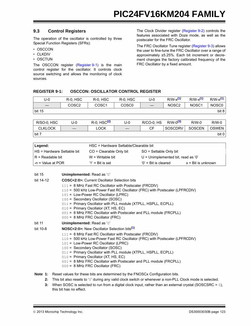
PIC24FV16KM204 FAMILY
9.3 Control Registers
The operation of the oscillator is controlled by threeSpecial Function Registers (SFRs):
• OSCCON• CLKDIV• OSCTUN
The OSCCON register (Register 9-1) is the maincontrol register for the oscillator. It controls clocksource switching and allows the monitoring of clocksources.
The Clock Divider register (Register 9-2) controls thefeatures associated with Doze mode, as well as thepostscaler for the FRC Oscillator.
The FRC Oscillator Tune register (Register 9-3) allowsthe user to fine-tune the FRC Oscillator over a range ofapproximately ±5.25%. Each bit increment or decre-ment changes the factory calibrated frequency of theFRC Oscillator by a fixed amount.
REGISTER 9-1: OSCCON: OSCILLATOR CONTROL REGISTER
U-0 R-0, HSC R-0, HSC R-0, HSC U-0 R/W-x(1) R/W-x(1) R/W-x(1)
— COSC2 COSC1 COSC0 — NOSC2 NOSC1 NOSC0
bit 15 bit 8
R/SO-0, HSC U-0 R-0, HSC(2) U-0 R/CO-0, HS R/W-0(3) R/W-0 R/W-0
CLKLOCK — LOCK — CF SOSCDRV SOSCEN OSWEN
bit 7 bit 0
Legend: HSC = Hardware Settable/Clearable bit
HS = Hardware Settable bit CO = Clearable Only bit SO = Settable Only bit
R = Readable bit W = Writable bit U = Unimplemented bit, read as ‘0’
-n = Value at POR ‘1’ = Bit is set ‘0’ = Bit is cleared x = Bit is unknown
bit 15 Unimplemented: Read as ‘0’
bit 14-12 COSC<2:0>: Current Oscillator Selection bits
111 = 8 MHz Fast RC Oscillator with Postscaler (FRCDIV)110 = 500 kHz Low-Power Fast RC Oscillator (FRC) with Postscaler (LPFRCDIV)101 = Low-Power RC Oscillator (LPRC)100 = Secondary Oscillator (SOSC)011 = Primary Oscillator with PLL module (XTPLL, HSPLL, ECPLL)010 = Primary Oscillator (XT, HS, EC)001 = 8 MHz FRC Oscillator with Postscaler and PLL module (FRCPLL)000 = 8 MHz FRC Oscillator (FRC)
bit 11 Unimplemented: Read as ‘0’
bit 10-8 NOSC<2:0>: New Oscillator Selection bits(1)
111 = 8 MHz Fast RC Oscillator with Postscaler (FRCDIV)110 = 500 kHz Low-Power Fast RC Oscillator (FRC) with Postscaler (LPFRCDIV)101 = Low-Power RC Oscillator (LPRC)100 = Secondary Oscillator (SOSC)011 = Primary Oscillator with PLL module (XTPLL, HSPLL, ECPLL)010 = Primary Oscillator (XT, HS, EC)001 = 8 MHz FRC Oscillator with Postscaler and PLL module (FRCPLL)000 = 8 MHz FRC Oscillator (FRC)
Note 1: Reset values for these bits are determined by the FNOSCx Configuration bits.
2: This bit also resets to ‘0’ during any valid clock switch or whenever a non-PLL Clock mode is selected.
3: When SOSC is selected to run from a digital clock input, rather than an external crystal (SOSCSRC = 0), this bit has no effect.
2013 Microchip Technology Inc. DS30003030B-page 123

PIC24FV16KM204 FAMILY
bit 7 CLKLOCK: Clock Selection Lock Enable bit
If FSCM is Enabled (FCKSM1 = 1):1 = Clock and PLL selections are locked0 = Clock and PLL selections are not locked and may be modified by setting the OSWEN bit
If FSCM is Disabled (FCKSM1 = 0):Clock and PLL selections are never locked and may be modified by setting the OSWEN bit.
bit 6 Unimplemented: Read as ‘0’
bit 5 LOCK: PLL Lock Status bit(2)
1 = PLL module is in lock or PLL module start-up timer is satisfied0 = PLL module is out of lock, PLL start-up timer is running or PLL is disabled
bit 4 Unimplemented: Read as ‘0’
bit 3 CF: Clock Fail Detect bit
1 = FSCM has detected a clock failure0 = No clock failure has been detected
bit 2 SOSCDRV: Secondary Oscillator Drive Strength bit(3)
1 = High-power SOSC circuit is selected 0 = Low/high-power select is done via the SOSCSRC Configuration bit
bit 1 SOSCEN: 32 kHz Secondary Oscillator (SOSC) Enable bit
1 = Enables the Secondary Oscillator0 = Disables the Secondary Oscillator
bit 0 OSWEN: Oscillator Switch Enable bit
1 = Initiates an oscillator switch to the clock source specified by the NOSC<2:0> bits0 = Oscillator switch is complete
REGISTER 9-1: OSCCON: OSCILLATOR CONTROL REGISTER (CONTINUED)
Note 1: Reset values for these bits are determined by the FNOSCx Configuration bits.
2: This bit also resets to ‘0’ during any valid clock switch or whenever a non-PLL Clock mode is selected.
3: When SOSC is selected to run from a digital clock input, rather than an external crystal (SOSCSRC = 0), this bit has no effect.
DS30003030B-page 124 2013 Microchip Technology Inc.

PIC24FV16KM204 FAMILY
REGISTER 9-2: CLKDIV: CLOCK DIVIDER REGISTER
R/W-0 R/W-0 R/W-1 R/W-1 R/W-0 R/W-0 R/W-0 R/W-1
ROI DOZE2 DOZE1 DOZE0 DOZEN(1) RCDIV2 RCDIV1 RCDIV0
bit 15 bit 8
U-0 U-0 U-0 U-0 U-0 U-0 U-0 U-0
— — — — — — — —
bit 7 bit 0
Legend:
R = Readable bit W = Writable bit U = Unimplemented bit, read as ‘0’
-n = Value at POR ‘1’ = Bit is set ‘0’ = Bit is cleared x = Bit is unknown
bit 15 ROI: Recover on Interrupt bit
1 = Interrupts clear the DOZEN bit, and reset the CPU and peripheral clock ratio to 1:10 = Interrupts have no effect on the DOZEN bit
bit 14-12 DOZE<2:0>: CPU and Peripheral Clock Ratio Select bits
111 = 1:128110 = 1:64101 = 1:32100 = 1:16011 = 1:8010 = 1:4001 = 1:2000 = 1:1
bit 11 DOZEN: Doze Enable bit(1)
1 = DOZE<2:0> bits specify the CPU and peripheral clock ratio0 = CPU and peripheral clock ratio are set to 1:1
bit 10-8 RCDIV<2:0>: FRC Postscaler Select bits
When COSC<2:0> (OSCCON<14:12>) = 111:111 = 31.25 kHz (divide-by-256)110 = 125 kHz (divide-by-64) 101 = 250 kHz (divide-by-32) 100 = 500 kHz (divide-by-16) 011 = 1 MHz (divide-by-8) 010 = 2 MHz (divide-by-4) 001 = 4 MHz (divide-by-2) – default000 = 8 MHz (divide-by-1)
When COSC<2:0> (OSCCON<14:12>) = 110:111 = 1.95 kHz (divide-by-256)110 = 7.81 kHz (divide-by-64) 101 = 15.62 kHz (divide-by-32) 100 = 31.25 kHz (divide-by-16) 011 = 62.5 kHz (divide-by-8) 010 = 125 kHz (divide-by-4) 001 = 250 kHz (divide-by-2) – default000 = 500 kHz (divide-by-1)
bit 7-0 Unimplemented: Read as ‘0’
Note 1: This bit is automatically cleared when the ROI bit is set and an interrupt occurs.
2013 Microchip Technology Inc. DS30003030B-page 125

PIC24FV16KM204 FAMILY
REGISTER 9-3: OSCTUN: FRC OSCILLATOR TUNE REGISTER
U-0 U-0 U-0 U-0 U-0 U-0 U-0 U-0
— — — — — — — —
bit 15 bit 8
U-0 U-0 R/W-0 R/W-0 R/W-0 R/W-0 R/W-0 R/W-0
— — TUN5(1) TUN4(1) TUN3(1) TUN2(1) TUN1(1) TUN0(1)
bit 7 bit 0
Legend:
R = Readable bit W = Writable bit U = Unimplemented bit, read as ‘0’
-n = Value at POR ‘1’ = Bit is set ‘0’ = Bit is cleared x = Bit is unknown
bit 15-6 Unimplemented: Read as ‘0’
bit 5-0 TUN<5:0>: FRC Oscillator Tuning bits(1)
011111 = Maximum frequency deviation011110•••000001000000 = Center frequency, oscillator is running at factory calibrated frequency111111•••100001100000 = Minimum frequency deviation
Note 1: Increments or decrements of TUN<5:0> may not change the FRC frequency in equal steps over the FRC tuning range and may not be monotonic.
DS30003030B-page 126 2013 Microchip Technology Inc.
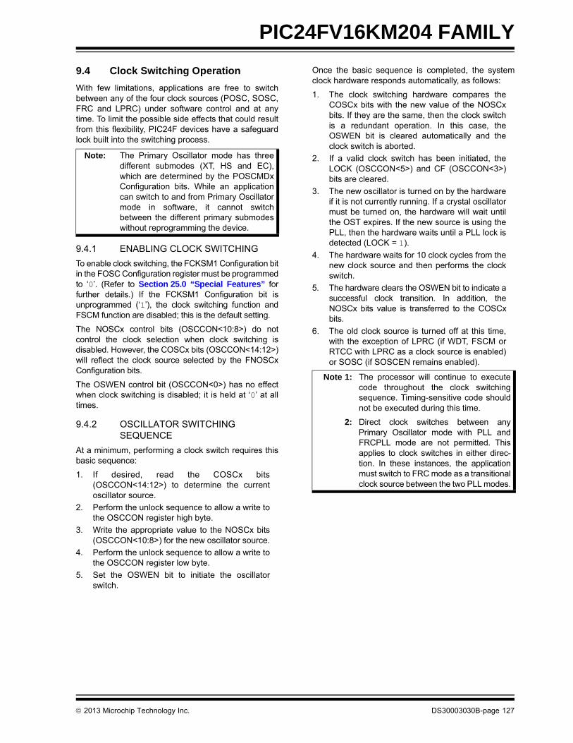
PIC24FV16KM204 FAMILY
9.4 Clock Switching Operation
With few limitations, applications are free to switchbetween any of the four clock sources (POSC, SOSC,FRC and LPRC) under software control and at anytime. To limit the possible side effects that could resultfrom this flexibility, PIC24F devices have a safeguardlock built into the switching process.
9.4.1 ENABLING CLOCK SWITCHING
To enable clock switching, the FCKSM1 Configuration bitin the FOSC Configuration register must be programmedto ‘0’. (Refer to Section 25.0 “Special Features” forfurther details.) If the FCKSM1 Configuration bit isunprogrammed (‘1’), the clock switching function andFSCM function are disabled; this is the default setting.
The NOSCx control bits (OSCCON<10:8>) do notcontrol the clock selection when clock switching isdisabled. However, the COSCx bits (OSCCON<14:12>)will reflect the clock source selected by the FNOSCxConfiguration bits.
The OSWEN control bit (OSCCON<0>) has no effectwhen clock switching is disabled; it is held at ‘0’ at alltimes.
9.4.2 OSCILLATOR SWITCHING SEQUENCE
At a minimum, performing a clock switch requires thisbasic sequence:
1. If desired, read the COSCx bits(OSCCON<14:12>) to determine the currentoscillator source.
2. Perform the unlock sequence to allow a write tothe OSCCON register high byte.
3. Write the appropriate value to the NOSCx bits(OSCCON<10:8>) for the new oscillator source.
4. Perform the unlock sequence to allow a write tothe OSCCON register low byte.
5. Set the OSWEN bit to initiate the oscillatorswitch.
Once the basic sequence is completed, the systemclock hardware responds automatically, as follows:
1. The clock switching hardware compares theCOSCx bits with the new value of the NOSCxbits. If they are the same, then the clock switchis a redundant operation. In this case, theOSWEN bit is cleared automatically and theclock switch is aborted.
2. If a valid clock switch has been initiated, theLOCK (OSCCON<5>) and CF (OSCCON<3>)bits are cleared.
3. The new oscillator is turned on by the hardwareif it is not currently running. If a crystal oscillatormust be turned on, the hardware will wait untilthe OST expires. If the new source is using thePLL, then the hardware waits until a PLL lock isdetected (LOCK = 1).
4. The hardware waits for 10 clock cycles from thenew clock source and then performs the clockswitch.
5. The hardware clears the OSWEN bit to indicate asuccessful clock transition. In addition, theNOSCx bits value is transferred to the COSCxbits.
6. The old clock source is turned off at this time,with the exception of LPRC (if WDT, FSCM orRTCC with LPRC as a clock source is enabled)or SOSC (if SOSCEN remains enabled).
Note: The Primary Oscillator mode has threedifferent submodes (XT, HS and EC),which are determined by the POSCMDxConfiguration bits. While an applicationcan switch to and from Primary Oscillatormode in software, it cannot switchbetween the different primary submodeswithout reprogramming the device.
Note 1: The processor will continue to executecode throughout the clock switchingsequence. Timing-sensitive code shouldnot be executed during this time.
2: Direct clock switches between anyPrimary Oscillator mode with PLL andFRCPLL mode are not permitted. Thisapplies to clock switches in either direc-tion. In these instances, the applicationmust switch to FRC mode as a transitionalclock source between the two PLL modes.
2013 Microchip Technology Inc. DS30003030B-page 127

PIC24FV16KM204 FAMILY
The following code sequence for a clock switch isrecommended:
1. Disable interrupts during the OSCCON registerunlock and write sequence.
2. Execute the unlock sequence for the OSCCONhigh byte by writing 78h and 9Ah toOSCCON<15:8>, in two back-to-backinstructions.
3. Write the new oscillator source to the NOSCxbits in the instruction immediately following theunlock sequence.
4. Execute the unlock sequence for the OSCCONlow byte by writing 46h and 57h toOSCCON<7:0>, in two back-to-back instructions.
5. Set the OSWEN bit in the instruction immediatelyfollowing the unlock sequence.
6. Continue to execute code that is notclock-sensitive (optional).
7. Invoke an appropriate amount of software delay(cycle counting) to allow the selected oscillatorand/or PLL to start and stabilize.
8. Check to see if OSWEN is ‘0’. If it is, the switchwas successful. If OSWEN is still set, then checkthe LOCK bit to determine the cause of failure.
The core sequence for unlocking the OSCCON registerand initiating a clock switch is shown in Example 9-1and Example 9-2.
EXAMPLE 9-1: ASSEMBLY CODE SEQUENCE FOR CLOCK SWITCHING
EXAMPLE 9-2: BASIC ‘C’ CODE SEQUENCE FOR CLOCK SWITCHING
9.5 Reference Clock Output
In addition to the CLKO output (FOSC/2) available incertain oscillator modes, the device clock in thePIC24FXXXXX family devices can also be configuredto provide a reference clock output signal to a port pin.This feature is available in all oscillator configurationsand allows the user to select a greater range of clocksubmultiples to drive external devices in theapplication.
This reference clock output is controlled by theREFOCON register (Register 9-4). Setting the ROEN bit(REFOCON<15>) makes the clock signal available onthe REFO pin. The RODIV<3:0> bits (REFOCON<11:8>)enable the selection of 16 different clock divider options.
The ROSSLP and ROSEL bits (REFOCON<13:12>)control the availability of the reference output duringSleep mode. The ROSEL bit determines if the oscillatoron OSC1 and OSC2, or the current system clocksource, is used for the reference clock output. TheROSSLP bit determines if the reference source isavailable on REFO when the device is in Sleep mode.
To use the reference clock output in Sleep mode, boththe ROSSLP and ROSEL bits must be set. The deviceclock must also be configured for one of the primarymodes (EC, HS or XT); otherwise, if the ROSEL bit isnot also set, the oscillator on OSC1 and OSC2 will bepowered down when the device enters Sleep mode.Clearing the ROSEL bit allows the reference outputfrequency to change as the system clock changesduring any clock switches.
;Place the new oscillator selection in W0;OSCCONH (high byte) Unlock SequenceMOV #OSCCONH, w1MOV #0x78, w2MOV #0x9A, w3MOV.b w2, [w1]MOV.b w3, [w1];Set new oscillator selectionMOV.b WREG, OSCCONH;OSCCONL (low byte) unlock sequenceMOV #OSCCONL, w1MOV #0x46, w2MOV #0x57, w3MOV.b w2, [w1]MOV.b w3, [w1];Start oscillator switch operationBSET OSCCON,#0
//Use compiler built-in function to write new clock setting__builtin_write_OSCCONH(0x01); //0x01 switches to FRCPLL
//Use compiler built-in function to set the OSWEN bit.__builtin_write_OSCCONL(OSCCONL | 0x01);
//Optional: Wait for clock switch sequence to completewhile(OSCCONbits.OSWEN == 1);
DS30003030B-page 128 2013 Microchip Technology Inc.

PIC24FV16KM204 FAMILY
REGISTER 9-4: REFOCON: REFERENCE OSCILLATOR CONTROL REGISTER
R/W-0 U-0 R/W-0 R/W-0 R/W-0 R/W-0 R/W-0 R/W-0
ROEN — ROSSLP ROSEL RODIV3 RODIV2 RODIV1 RODIV0
bit 15 bit 8
U-0 U-0 U-0 U-0 U-0 U-0 U-0 U-0
— — — — — — — —
bit 7 bit 0
Legend:
R = Readable bit W = Writable bit U = Unimplemented bit, read as ‘0’
-n = Value at POR ‘1’ = Bit is set ‘0’ = Bit is cleared x = Bit is unknown
bit 15 ROEN: Reference Oscillator Output Enable bit
1 = Reference Oscillator is enabled on the REFO pin0 = Reference Oscillator is disabled
bit 14 Unimplemented: Read as ‘0’
bit 13 ROSSLP: Reference Oscillator Output Stop in Sleep bit
1 = Reference Oscillator continues to run in Sleep0 = Reference Oscillator is disabled in Sleep
bit 12 ROSEL: Reference Oscillator Source Select bit
1 = Primary Oscillator is used as the base clock(1)
0 = System clock is used as the base clock; base clock reflects any clock switching of the device
bit 11-8 RODIV<3:0>: Reference Oscillator Divisor Select bits
1111 = Base clock value divided by 32,7681110 = Base clock value divided by 16,3841101 = Base clock value divided by 8,1921100 = Base clock value divided by 4,0961011 = Base clock value divided by 2,0481010 = Base clock value divided by 1,0241001 = Base clock value divided by 5121000 = Base clock value divided by 2560111 = Base clock value divided by 1280110 = Base clock value divided by 640101 = Base clock value divided by 320100 = Base clock value divided by 160011 = Base clock value divided by 80010 = Base clock value divided by 40001 = Base clock value divided by 20000 = Base clock value
bit 7-0 Unimplemented: Read as ‘0’
Note 1: The crystal oscillator must be enabled using the FOSC<2:0> bits; the crystal maintains the operation in Sleep mode.
2013 Microchip Technology Inc. DS30003030B-page 129

PIC24FV16KM204 FAMILY
NOTES:
DS30003030B-page 130 2013 Microchip Technology Inc.

PIC24FV16KM204 FAMILY
10.0 POWER-SAVING FEATURES
The PIC24FV16KM204 family of devices provides theability to manage power consumption by selectivelymanaging clocking to the CPU and the peripherals. Ingeneral, a lower clock frequency and a reduction in thenumber of circuits being clocked constitutes lowerconsumed power. All PIC24F devices manage powerconsumption in four different ways:
• Clock Frequency
• Instruction-Based Sleep and Idle modes
• Software Controlled Doze mode
• Selective Peripheral Control in Software
Combinations of these methods can be used toselectively tailor an application’s power consumption,while still maintaining critical application features, suchas timing-sensitive communications.
10.1 Clock Frequency and Clock Switching
PIC24F devices allow for a wide range of clockfrequencies to be selected under application control. Ifthe system clock configuration is not locked, users canchoose low-power or high-precision oscillators by simplychanging the NOSCx bits. The process of changing asystem clock during operation, as well as limitations tothe process, are discussed in more detail in Section 9.0“Oscillator Configuration”.
10.2 Instruction-Based Power-Saving Modes
PIC24F devices have two special power-saving modesthat are entered through the execution of a specialPWRSAV instruction. Sleep mode stops clock operationand halts all code execution; Idle mode halts the CPUand code execution, but allows peripheral modules tocontinue operation.
The ‘C’ syntax of the PWRSAV instruction is shown inExample 10-1.
Sleep and Idle modes can be exited as a result of anenabled interrupt, WDT time-out or a device Reset.When the device exits these modes, it is said to“wake-up”.
10.2.1 SLEEP MODE
Sleep mode includes these features:
• The system clock source is shut down. If an on-chip oscillator is used, it is turned off.
• The device current consumption will be reduced to a minimum provided that no I/O pin is sourcing current.
• The I/O pin directions and states are frozen.
• The Fail-Safe Clock Monitor does not operate during Sleep mode since the system clock source is disabled.
• The LPRC clock will continue to run in Sleep mode if the WDT or RTCC with LPRC as the clock source is enabled.
• The WDT, if enabled, is automatically cleared prior to entering Sleep mode.
• Some device features or peripherals may continue to operate in Sleep mode. This includes items, such as the Input Change Notification on the I/O ports or peripherals that use an External Clock input. Any peripheral that requires the sys-tem clock source for its operation will be disabled in Sleep mode.
The device will wake-up from Sleep mode on any ofthese events:
• On any interrupt source that is individually enabled
• On any form of device Reset
• On a WDT time-out
On wake-up from Sleep, the processor will restart withthe same clock source that was active when Sleepmode was entered.
EXAMPLE 10-1: ‘C’ POWER-SAVING ENTRY
Note: This data sheet summarizes the features ofthis group of PIC24F devices. It is notintended to be a comprehensive referencesource. For more information, refer to the“PIC24F Family Reference Manual”,“Power-Saving Features with VBAT”(DS30622).
This FRM describes some features whichare not implemented in this device. Sectionsrelated to the VBAT pin and Deep Sleep donot apply to the PIC24FV16KM204 family.
Note: SLEEP_MODE and IDLE_MODE areconstants defined in the assemblerinclude file for the selected device.
Sleep(); //Put the device into Sleep modeIdle(); //Put the device into Idle mode
2013 Microchip Technology Inc. DS30003030B-page 131

PIC24FV16KM204 FAMILY
10.2.2 IDLE MODEIdle mode includes these features:
• The CPU will stop executing instructions.• The WDT is automatically cleared.• The system clock source remains active. By
default, all peripheral modules continue to operate normally from the system clock source, but can also be selectively disabled (see Section 10.6 “Selective Peripheral Module Control”).
• If the WDT or FSCM is enabled, the LPRC will also remain active.
The device will wake from Idle mode on any of theseevents:
• Any interrupt that is individually enabled• Any device Reset• A WDT time-out
On wake-up from Idle, the clock is reapplied to the CPUand instruction execution begins immediately, startingwith the instruction following the PWRSAV instruction orthe first instruction in the ISR.
10.2.3 INTERRUPTS COINCIDENT WITH POWER SAVE INSTRUCTIONS
Any interrupt that coincides with the execution of aPWRSAV instruction will be held off until entry into Sleepor Idle mode has completed. The device will thenwake-up from Sleep or Idle mode.
10.2.3.1 Power-on Resets (PORs)
VDD voltage is monitored to produce PORs. When a truePOR occurs, the entire device is reset.
10.3 Ultra Low-Power Wake-up
The Ultra Low-Power Wake-up (ULPWU) on pin, RB0,allows a slow falling voltage to generate an interruptwithout excess current consumption.
To use this feature:
1. Charge the capacitor on RB0 by configuring theRB0 pin to an output and setting it to ‘1’.
2. Stop charging the capacitor by configuring RB0as an input.
3. Discharge the capacitor by setting the ULPENand ULPSINK bits in the ULPWCON register.
4. Configure Sleep mode.5. Enter Sleep mode.
When the voltage on RB0 drops below VIL, the devicewakes up and executes the next instruction.
This feature provides a low-power technique forperiodically waking up the device from Sleep mode.
The time-out is dependent on the discharge time of theRC circuit on RB0.
When the ULPWU module wakes the device fromSleep mode, the ULPWUIF bit (IFS5<0>) is set. Soft-ware can check this bit upon wake-up to determine thewake-up source.
See Example 10-2 for initializing the ULPWU module.
EXAMPLE 10-2: ULTRA LOW-POWER WAKE-UP INITIALIZATION
A series resistor, between RB0 and the externalcapacitor provides overcurrent protection for theAN2/ULPWU/RB0 pin and enables software calibrationof the time-out (see Figure 10-1).
FIGURE 10-1: SERIES RESISTOR
A timer can be used to measure the charge time anddischarge time of the capacitor. The charge time canthen be adjusted to provide the desired delay in Sleep.This technique compensates for the affects of temper-ature, voltage and component accuracy. The peripheralcan also be configured as a simple, programmableLow-Voltage Detect (LVD) or temperature sensor.
//*******************************// 1. Charge the capacitor on RB0//******************************* TRISBbits.TRISB0 = 0; LATBbits.LATB0 = 1; for(i = 0; i < 10000; i++) Nop();//*****************************//2. Stop Charging the capacitor// on RB0//***************************** TRISBbits.TRISB0 = 1;//*****************************//3. Enable ULPWU Interrupt//*****************************IFS5bits.ULPWUIF = 0;IEC5bits.ULPWUIE = 1;IPC21bits.ULPWUIP = 0x7;//*****************************//4. Enable the Ultra Low Power// Wakeup module and allow// capacitor discharge//***************************** ULPWCONbits.ULPEN = 1; ULPWCONbit.ULPSINK = 1;//*****************************//5. Enter Sleep Mode//***************************** Sleep();//for sleep, execution will//resume here
R1
C1
RB0
DS30003030B-page 132 2013 Microchip Technology Inc.

PIC24FV16KM204 FAMILY
REGISTER 10-1: ULPWCON: ULPWU CONTROL REGISTER
R/W-0 U-0 R/W-0 U-0 U-0 U-0 U-0 R/W-0
ULPEN — ULPSIDL — — — — ULPSINK
bit 15 bit 8
U-0 U-0 U-0 U-0 U-0 U-0 U-0 U-0
— — — — — — — —
bit 7 bit 0
Legend:
R = Readable bit W = Writable bit U = Unimplemented bit, read as ‘0’
-n = Value at POR ‘1’ = Bit is set ‘0’ = Bit is cleared x = Bit is unknown
bit 15 ULPEN: ULPWU Module Enable bit
1 = Module is enabled0 = Module is disabled
bit 14 Unimplemented: Read as ‘0’
bit 13 ULPSIDL: ULPWU Stop in Idle Select bit
1 = Discontinues module operation when the device enters Idle mode0 = Continues module operation in Idle mode
bit 12-9 Unimplemented: Read as ‘0’
bit 8 ULPSINK: ULPWU Current Sink Enable bit
1 = Current sink is enabled0 = Current sink is disabled
bit 7-0 Unimplemented: Read as ‘0’
2013 Microchip Technology Inc. DS30003030B-page 133

PIC24FV16KM204 FAMILY
10.4 Voltage Regulator-Based Power-Saving Features
The PIC24FV16KM204 family series devices have avoltage regulator that has the ability to alterfunctionality to provide power savings. The on-chipregulator is made up of two basic modules: the VoltageRegulator (VREG) and the Retention Regulator(RETREG). With the combination of VREG andRETREG, the following power modes are available:
10.4.1 RUN MODE
In Run mode, the main VREG is providing a regulatedvoltage with enough current to supply a device runningat full speed and the device is not in Sleep mode. TheRETREG may or may not be running, but is unused.
10.4.2 SLEEP MODE
In Sleep mode, the device is in Sleep and the mainVREG is providing a regulated voltage to the core. Bydefault, in Sleep mode, the regulator enters alow-power standby state which consumes reducedquiescent current. The PMSLP bit (RCON<8>) controlsthe regulator state in Sleep mode. If the PMSLP bit isset, the program Flash memory will stay powered onduring Sleep mode and the regulator will stay in itsfull-power mode.
10.4.3 RETENTION REGULATOR
The Retention Regulator, sometimes referred to as thelow-voltage regulator, is designed to provide power tothe core at a lower voltage than the standard voltageregulator, while consuming significantly lower quiescentcurrent. Refer to Section 27.0 “Electrical Characteris-tics” for the voltage output range of the RETREG. Thisregulator is only used in Sleep mode, and has limitedoutput current to maintain the RAM and provide powerfor limited peripherals, such as the WDT, while thedevice is in Sleep. It is controlled by the RETCFG Con-figuration bit (FPOR<2>) and in firmware by the RETENbit (RCON<12>). RETCFG must be programmed (= 0)and the RETEN bit must be set (= 1) for the RetentionRegulator to be enabled.
10.4.4 RETENTION SLEEP MODE
In Retention Sleep mode, the device is in Sleep and allregulated voltage is provided solely by the RETREG,while the main VREG is disabled. Consequently, thismode provides the lowest Sleep power consumption,but has a trade-off of a longer wake-up time. Thelow-voltage Sleep wake-up time is longer than Sleepmode due to the extra time required to re-enable theVREG and raise the VDDCORE supply rail back tonormal regulated levels.
TABLE 10-1: VOLTAGE REGULATION CONFIGURATION SETTINGS FOR PIC24FXXXXX FAMILY DEVICES
Note: The PIC24F16KM204 family devices donot have any internal voltage regulation,and therefore, do not support RetentionSleep mode.
RETCFG Bit (FPOR<2>)
RETEN Bit (RCON<12>
PMSLP Bit (RCON<8>)
Power ModeDuring Sleep
Description
0 0 1 Sleep VREG mode (normal) is unchanged during Sleep.
RETREG is unused.
0 0 0 Sleep VREG goes to Low-Power Standby mode during Sleep.
(Standby) RETREG is unused.
0 1 0 Retention Sleep
VREG is off during Sleep.
RETREG is enabled and provides Sleep voltage regulation.
1 x 1 Sleep VREG mode (normal) is unchanged during Sleep.
RETREG is disabled at all times.
1 x 0 Sleep VREG goes to Low-Power Standby mode during Sleep.
(Standby) RETREG is disabled at all times.
DS30003030B-page 134 2013 Microchip Technology Inc.

PIC24FV16KM204 FAMILY
10.5 Doze Mode
Generally, changing clock speed and invoking one ofthe power-saving modes are the preferred strategiesfor reducing power consumption. There may becircumstances, however, where this is not practical. Forexample, it may be necessary for an application tomaintain uninterrupted synchronous communication,even while it is doing nothing else. Reducing systemclock speed may introduce communication errors,while using a power-saving mode may stopcommunications completely.
Doze mode is a simple and effective alternative methodto reduce power consumption while the device is stillexecuting code. In this mode, the system clock contin-ues to operate from the same source and at the samespeed. Peripheral modules continue to be clocked atthe same speed, while the CPU clock speed isreduced. Synchronization between the two clockdomains is maintained, allowing the peripherals toaccess the SFRs while the CPU executes code at aslower rate.
Doze mode is enabled by setting the DOZEN bit(CLKDIV<11>). The ratio between peripheral andcore clock speed is determined by the DOZE<2:0>bits (CLKDIV<14:12>). There are eight possibleconfigurations, from 1:1 to 1:128, with 1:1 being thedefault.
It is also possible to use Doze mode to selectivelyreduce power consumption in event driven applica-tions. This allows clock-sensitive functions, such assynchronous communications, to continue withoutinterruption. Meanwhile, the CPU Idles, waiting forsomething to invoke an interrupt routine. Enabling theautomatic return to full-speed CPU operation on inter-rupts is enabled by setting the ROI bit (CLKDIV<15>).By default, interrupt events have no effect on Dozemode operation.
10.6 Selective Peripheral Module Control
Idle and Doze modes allow users to substantiallyreduce power consumption by slowing or stopping theCPU clock. Even so, peripheral modules still remainclocked, and thus, consume power. There may becases where the application needs what these modesdo not provide: the allocation of power resources toCPU processing with minimal power consumption fromthe peripherals.
PIC24F devices address this requirement by allowingperipheral modules to be selectively disabled, reducingor eliminating their power consumption. This can bedone with two control bits:
• The Peripheral Enable bit, generically named, “XXXEN”, located in the module’s main control SFR.
• The Peripheral Module Disable (PMD) bit, generically named, “XXXMD”, located in one of the PMDx Control registers.
Both bits have similar functions in enabling or disablingits associated module. Setting the PMDx bits for amodule, disables all clock sources to that module, reduc-ing its power consumption to an absolute minimum. Inthis state, the control and status registers associatedwith the peripheral will also be disabled, so writes tothose registers will have no effect, and read values willbe invalid. Many peripheral modules have acorresponding PMDx bit.
In contrast, disabling a module by clearing its XXXENbit, disables its functionality, but leaves its registersavailable to be read and written to. Power consumptionis reduced, but not by as much as when the PMDx bitsare used. Most peripheral modules have an enable bit;exceptions include capture, compare and RTCC.
To achieve more selective power savings, peripheralmodules can also be selectively disabled when thedevice enters Idle mode. This is done through the controlbit of the generic name format, “XXXIDL”. By default, allmodules that can operate during Idle mode will do so.Using the disable on Idle feature disables the modulewhile in Idle mode, allowing further reduction of powerconsumption during Idle mode, enhancing powersavings for extremely critical power applications.
2013 Microchip Technology Inc. DS30003030B-page 135

PIC24FV16KM204 FAMILY
NOTES:
DS30003030B-page 136 2013 Microchip Technology Inc.
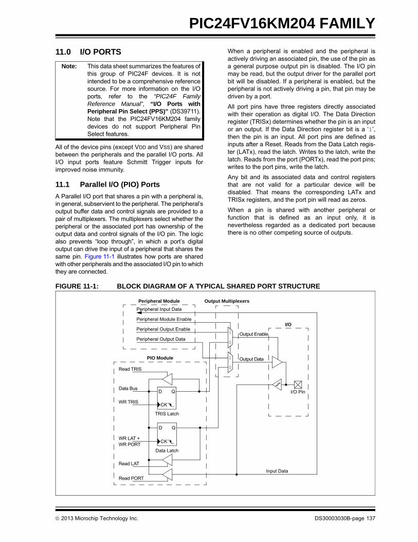
PIC24FV16KM204 FAMILY
11.0 I/O PORTS
All of the device pins (except VDD and VSS) are sharedbetween the peripherals and the parallel I/O ports. AllI/O input ports feature Schmitt Trigger inputs forimproved noise immunity.
11.1 Parallel I/O (PIO) Ports
A Parallel I/O port that shares a pin with a peripheral is,in general, subservient to the peripheral. The peripheral’soutput buffer data and control signals are provided to apair of multiplexers. The multiplexers select whether theperipheral or the associated port has ownership of theoutput data and control signals of the I/O pin. The logicalso prevents “loop through”, in which a port’s digitaloutput can drive the input of a peripheral that shares thesame pin. Figure 11-1 illustrates how ports are sharedwith other peripherals and the associated I/O pin to whichthey are connected.
When a peripheral is enabled and the peripheral isactively driving an associated pin, the use of the pin asa general purpose output pin is disabled. The I/O pinmay be read, but the output driver for the parallel portbit will be disabled. If a peripheral is enabled, but theperipheral is not actively driving a pin, that pin may bedriven by a port.
All port pins have three registers directly associatedwith their operation as digital I/O. The Data Directionregister (TRISx) determines whether the pin is an inputor an output. If the Data Direction register bit is a ‘1’,then the pin is an input. All port pins are defined asinputs after a Reset. Reads from the Data Latch regis-ter (LATx), read the latch. Writes to the latch, write thelatch. Reads from the port (PORTx), read the port pins;writes to the port pins, write the latch.
Any bit and its associated data and control registersthat are not valid for a particular device will bedisabled. That means the corresponding LATx andTRISx registers, and the port pin will read as zeros.
When a pin is shared with another peripheral orfunction that is defined as an input only, it isnevertheless regarded as a dedicated port becausethere is no other competing source of outputs.
FIGURE 11-1: BLOCK DIAGRAM OF A TYPICAL SHARED PORT STRUCTURE
Note: This data sheet summarizes the features ofthis group of PIC24F devices. It is notintended to be a comprehensive referencesource. For more information on the I/Oports, refer to the “PIC24F FamilyReference Manual”, “I/O Ports withPeripheral Pin Select (PPS)” (DS39711).Note that the PIC24FV16KM204 familydevices do not support Peripheral PinSelect features.
QD
CK
WR LAT +
TRIS Latch
I/O Pin
WR PORT
Data Bus
QD
CK
Data Latch
Read PORT
Read TRIS
1
0
1
0
WR TRIS
Peripheral Output Data
Peripheral Input Data
I/O
Peripheral Module
Peripheral Output Enable
PIO Module
Output Multiplexers
Output Data
Input Data
Peripheral Module Enable
Read LAT
Output Enable
2013 Microchip Technology Inc. DS30003030B-page 137

PIC24FV16KM204 FAMILY
11.1.1 OPEN-DRAIN CONFIGURATION
In addition to the PORT, LAT and TRIS registers fordata control, each port pin can also be individually con-figured for either digital or open-drain output. This iscontrolled by the Open-Drain Control register, ODCx,associated with each port. Setting any of the bitsconfigures the corresponding pin to act as anopen-drain output.
The maximum open-drain voltage allowed is the sameas the maximum VIH specification.
11.2 Configuring Analog Port Pins
The use of the ANSx and TRISx registers controls theoperation of the A/D port pins. The port pins that aredesired as analog inputs must have their correspond-ing TRISx bit set (input). If the TRISx bit is cleared(output), the digital output level (VOH or VOL) will beconverted.
When reading the PORTx register, all pins configuredas analog input channels will read as cleared (a lowlevel). Analog levels on any pin that is defined as a dig-ital input (including the ANx pins) may cause the inputbuffer to consume current that exceeds the devicespecifications.
11.2.1 ANALOG SELECTION REGISTER
I/O pins with shared analog functionality, such as A/Dinputs and comparator inputs, must have their digitalinputs shut off when analog functionality is used. Notethat analog functionality includes an analog voltagebeing applied to the pin externally.
To allow for analog control, the ANSx registers areprovided. There is one ANSx register for each port(ANSA, ANSB and ANSC). Within each ANSx register,there is a bit for each pin that shares analogfunctionality with the digital I/O functionality.
If a particular pin does not have an analog function, thatbit is unimplemented. See Register 11-1 to Register 11-3for implementation.
REGISTER 11-1: ANSA: PORTA ANALOG SELECTION REGISTER
U-0 U-0 U-0 U-0 U-0 U-0 U-0 U-0
— — — — — — — —
bit 15 bit 8
U-0 U-0 U-0 R/W-1 R/W-1 R/W-1 R/W-1 R/W-1
— — — ANSA4(1) ANSA3 ANSA2 ANSA1 ANSA0
bit 7 bit 0
Legend:
R = Readable bit W = Writable bit U = Unimplemented bit, read as ‘0’
-n = Value at POR ‘1’ = Bit is set ‘0’ = Bit is cleared x = Bit is unknown
bit 15-5 Unimplemented: Read as ‘0’
bit 4-0 ANSA<4:0>: Analog Select Control bits(1)
1 = Digital input buffer is not active (use for analog input)0 = Digital input buffer is active
Note 1: The ANSA4 bit is not available on 20-pin devices.
DS30003030B-page 138 2013 Microchip Technology Inc.

PIC24FV16KM204 FAMILY
REGISTER 11-2: ANSB: PORTB ANALOG SELECTION REGISTER
R/W-1 R/W-1 R/W-1 R/W-1 U-0 U-0 R/W-1 R/W-1
ANSB15 ANSB14 ANSB13 ANSB12 — — ANSB9 ANSB8
bit 15 bit 8
R/W-1 R/W-1 R/W-1 R/W-1 R/W-1 R/W-1 R/W-1 R/W-1
ANSB7 ANSB6(1) ANSB5(1) ANSB4 ANSB3(1) ANSB2 ANSB1 ANSB0
bit 7 bit 0
Legend:
R = Readable bit W = Writable bit U = Unimplemented bit, read as ‘0’
-n = Value at POR ‘1’ = Bit is set ‘0’ = Bit is cleared x = Bit is unknown
bit 15-12 ANSB<15:12>: Analog Select Control bits
1 = Digital input buffer is not active (use for analog input)0 = Digital input buffer is active
bit 11-10 Unimplemented: Read as ‘0’
bit 9-0 ANSB<9:0>: Analog Select Control bits(1)
1 = Digital input buffer is not active (use for analog input)0 = Digital input buffer is active
Note 1: The ANSB<6:5,3> bits are not available on 20-pin devices.
REGISTER 11-3: ANSC: PORTC ANALOG SELECTION REGISTER
U-0 U-0 U-0 U-0 U-0 U-0 U-0 U-0
— — — — — — — —
bit 15 bit 8
U-0 U-0 U-0 U-0 U-0 R/W-1 R/W-1 R/W-1
— — — — — ANSC2(1,2) ANSC1(1,2) ANSC0(1,2)
bit 7 bit 0
Legend:
R = Readable bit W = Writable bit U = Unimplemented bit, read as ‘0’
-n = Value at POR ‘1’ = Bit is set ‘0’ = Bit is cleared x = Bit is unknown
bit 15-3 Unimplemented: Read as ‘0’
bit 2-0 ANSC<2:0>: Analog Select Control bits(1,2)
1 = Digital input buffer is not active (use for analog input)0 = Digital input buffer is active
Note 1: These bits are not implemented in 20-pin devices.
2: These bits are not implemented in 28-pin devices.
2013 Microchip Technology Inc. DS30003030B-page 139

PIC24FV16KM204 FAMILY
11.2.2 I/O PORT WRITE/READ TIMING
One instruction cycle is required between a portdirection change or port write operation, and a readoperation of the same port. Typically, this instructionwould be a NOP.
11.3 Input Change Notification (ICN)
The Input Change Notification function of the I/O portsallows the PIC24FXXXXX family of devices to generateinterrupt requests to the processor in response to aChange-of-State (COS) on selected input pins. Thisfeature is capable of detecting input Change-of-States,even in Sleep mode, when the clocks are disabled.Depending on the device pin count, there are up to37 external signals (CN0 through CN36) that may beselected (enabled) for generating an interrupt requeston a Change-of-State.
There are six control registers associated with the CNmodule. The CNEN1 and CNEN3 registers contain theinterrupt enable control bits for each of the CNx inputpins. Setting any of these bits enables a CN interruptfor the corresponding pins.
Each CNx pin also has a weak pull-up/pull-downconnected to it. The pull-ups act as a current sourcethat is connected to the pin. The pull-downs act as acurrent sink to eliminate the need for external resistorswhen push button or keypad devices are connected.
On any pin, only the pull-up resistor or the pull-downresistor should be enabled, but not both of them. If thepush button or the keypad is connected to VDD, enablethe pull-down, or if they are connected to VSS, enablethe pull-up resistors. The pull-ups are enabledseparately using the CNPU1 and CNPU3 registers,which contain the control bits for each of the CNx pins.
Setting any of the control bits enables the weakpull-ups for the corresponding pins. The pull-downs areenabled separately using the CNPD1 and CNPD3registers, which contain the control bits for each of theCNx pins. Setting any of the control bits enables theweak pull-downs for the corresponding pins.
When the internal pull-up is selected, the pin uses VDD
as the pull-up source voltage. When the internalpull-down is selected, the pins are pulled down to VSS
by an internal resistor. Make sure that there is noexternal pull-up source/pull-down sink when theinternal pull-ups/pull-downs are enabled.
EXAMPLE 11-1: PORT WRITE/READ EXAMPLE
Note: Pull-ups and pull-downs on Change Notifi-cation (CN) pins should always be disabledwhenever the port pin is configured as adigital output.
MOV 0xFF00, W0; //Configure PORTB<15:8> as inputs and PORTB<7:0> as outputsMOV W0, TRISB; NOP; //Delay 1 cycleBTSS PORTB, #13; //Next Instruction
Equivalent ‘C’ Code TRISB = 0xFF00; //Configure PORTB<15:8> as inputs and PORTB<7:0> as outputsNOP(); //Delay 1 cycleif(PORTBbits.RB13 == 1) // execute following code if PORTB pin 13 is set.
DS30003030B-page 140 2013 Microchip Technology Inc.
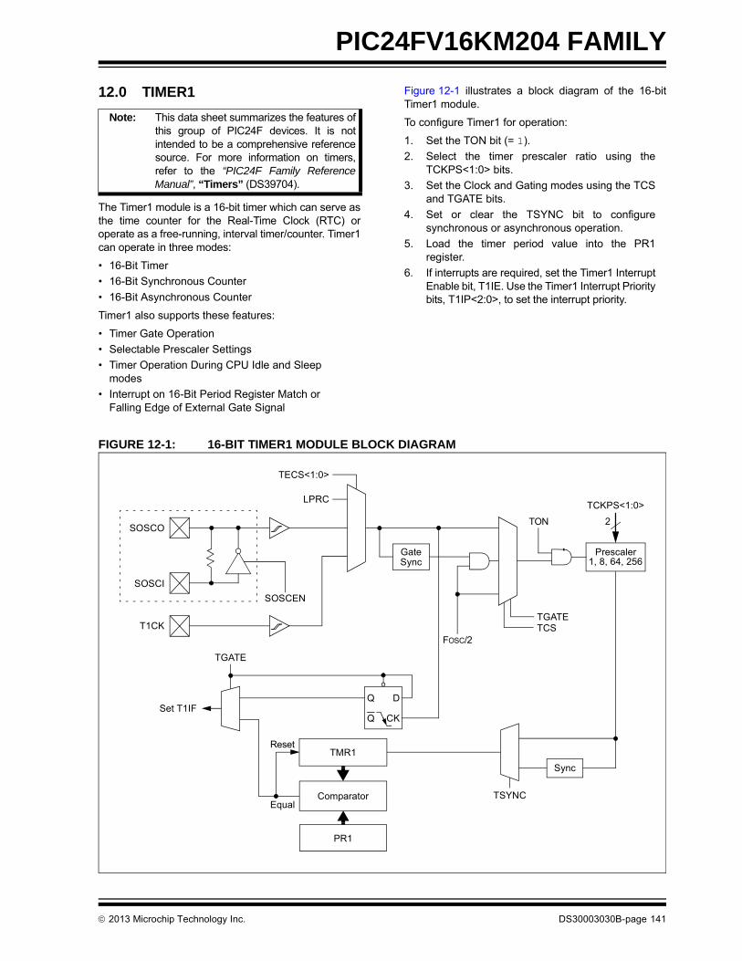
PIC24FV16KM204 FAMILY
12.0 TIMER1
The Timer1 module is a 16-bit timer which can serve asthe time counter for the Real-Time Clock (RTC) oroperate as a free-running, interval timer/counter. Timer1can operate in three modes:
• 16-Bit Timer
• 16-Bit Synchronous Counter
• 16-Bit Asynchronous Counter
Timer1 also supports these features:
• Timer Gate Operation
• Selectable Prescaler Settings
• Timer Operation During CPU Idle and Sleep modes
• Interrupt on 16-Bit Period Register Match or Falling Edge of External Gate Signal
Figure 12-1 illustrates a block diagram of the 16-bitTimer1 module.
To configure Timer1 for operation:
1. Set the TON bit (= 1).
2. Select the timer prescaler ratio using theTCKPS<1:0> bits.
3. Set the Clock and Gating modes using the TCSand TGATE bits.
4. Set or clear the TSYNC bit to configuresynchronous or asynchronous operation.
5. Load the timer period value into the PR1register.
6. If interrupts are required, set the Timer1 InterruptEnable bit, T1IE. Use the Timer1 Interrupt Prioritybits, T1IP<2:0>, to set the interrupt priority.
FIGURE 12-1: 16-BIT TIMER1 MODULE BLOCK DIAGRAM
Note: This data sheet summarizes the features ofthis group of PIC24F devices. It is notintended to be a comprehensive referencesource. For more information on timers,refer to the “PIC24F Family ReferenceManual”, “Timers” (DS39704).
TON
Sync
SOSCI
SOSCO
PR1
Set T1IF
Equal
Reset
SOSCEN
TSYNC
Q
Q D
CK
TCKPS<1:0>
Prescaler1, 8, 64, 256
2
TGATE
FOSC/2TCSTGATE
T1CK
TECS<1:0>
LPRC
Comparator
TMR1
GateSync
2013 Microchip Technology Inc. DS30003030B-page 141

PIC24FV16KM204 FAMILY
REGISTER 12-1: T1CON: TIMER1 CONTROL REGISTER
R/W-0 U-0 R/W-0 U-0 U-0 U-0 R/W-0 R/W-0
TON — TSIDL — — — TECS1(1) TECS0(1)
bit 15 bit 8
U-0 R/W-0 R/W-0 R/W-0 U-0 R/W-0 R/W-0 U-0
— TGATE TCKPS1 TCKPS0 — TSYNC TCS —
bit 7 bit 0
Legend:
R = Readable bit W = Writable bit U = Unimplemented bit, read as ‘0’
-n = Value at POR ‘1’ = Bit is set ‘0’ = Bit is cleared x = Bit is unknown
bit 15 TON: Timer1 On bit
1 = Starts 16-bit Timer10 = Stops 16-bit Timer1
bit 14 Unimplemented: Read as ‘0’
bit 13 TSIDL: Timer1 Stop in Idle Mode bit
1 = Discontinues module operation when device enters Idle mode0 = Continues module operation in Idle mode
bit 12-10 Unimplemented: Read as ‘0’
bit 9-8 TECS<1:0>: Timer1 Extended Clock Select bits(1)
11 = Reserved; do not use10 = Timer1 uses the LPRC as the clock source01 = Timer1 uses the External Clock (EC) from T1CK00 = Timer1 uses the Secondary Oscillator (SOSC) as the clock source
bit 7 Unimplemented: Read as ‘0’
bit 6 TGATE: Timer1 Gated Time Accumulation Enable bit
When TCS = 1:This bit is ignored.
When TCS = 0: 1 = Gated time accumulation is enabled0 = Gated time accumulation is disabled
bit 5-4 TCKPS<1:0>: Timer1 Input Clock Prescale Select bits
11 = 1:256 10 = 1:6401 = 1:8 00 = 1:1
bit 3 Unimplemented: Read as ‘0’
bit 2 TSYNC: Timer1 External Clock Input Synchronization Select bit
When TCS = 1: 1 = Synchronizes External Clock input0 = Does not synchronize External Clock input
When TCS = 0: This bit is ignored.
bit 1 TCS: Timer1 Clock Source Select bit
1 = Timer1 clock source is selected by TECS<1:0>0 = Internal clock (FOSC/2)
bit 0 Unimplemented: Read as ‘0’
Note 1: The TECSx bits are valid only when TCS = 1.
DS30003030B-page 142 2013 Microchip Technology Inc.
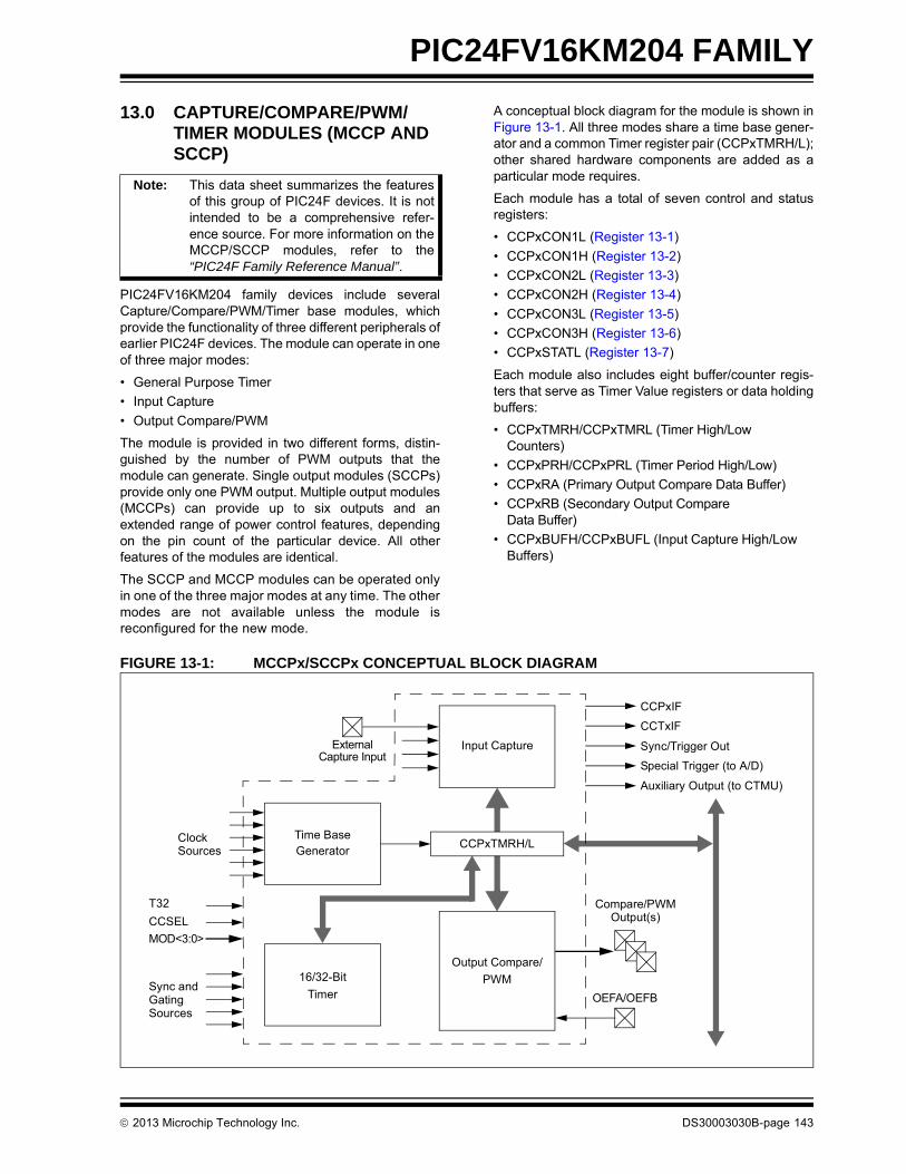
PIC24FV16KM204 FAMILY
13.0 CAPTURE/COMPARE/PWM/TIMER MODULES (MCCP AND SCCP)
PIC24FV16KM204 family devices include severalCapture/Compare/PWM/Timer base modules, whichprovide the functionality of three different peripherals ofearlier PIC24F devices. The module can operate in oneof three major modes:
• General Purpose Timer
• Input Capture
• Output Compare/PWM
The module is provided in two different forms, distin-guished by the number of PWM outputs that themodule can generate. Single output modules (SCCPs)provide only one PWM output. Multiple output modules(MCCPs) can provide up to six outputs and anextended range of power control features, dependingon the pin count of the particular device. All otherfeatures of the modules are identical.
The SCCP and MCCP modules can be operated onlyin one of the three major modes at any time. The othermodes are not available unless the module isreconfigured for the new mode.
A conceptual block diagram for the module is shown inFigure 13-1. All three modes share a time base gener-ator and a common Timer register pair (CCPxTMRH/L);other shared hardware components are added as aparticular mode requires.
Each module has a total of seven control and statusregisters:
• CCPxCON1L (Register 13-1)
• CCPxCON1H (Register 13-2)
• CCPxCON2L (Register 13-3)
• CCPxCON2H (Register 13-4)
• CCPxCON3L (Register 13-5)
• CCPxCON3H (Register 13-6)
• CCPxSTATL (Register 13-7)
Each module also includes eight buffer/counter regis-ters that serve as Timer Value registers or data holdingbuffers:
• CCPxTMRH/CCPxTMRL (Timer High/Low Counters)
• CCPxPRH/CCPxPRL (Timer Period High/Low)
• CCPxRA (Primary Output Compare Data Buffer)
• CCPxRB (Secondary Output Compare Data Buffer)
• CCPxBUFH/CCPxBUFL (Input Capture High/Low Buffers)
FIGURE 13-1: MCCPx/SCCPx CONCEPTUAL BLOCK DIAGRAM
Note: This data sheet summarizes the featuresof this group of PIC24F devices. It is notintended to be a comprehensive refer-ence source. For more information on theMCCP/SCCP modules, refer to the“PIC24F Family Reference Manual”.
ClockSources
Input Capture
Output Compare/
PWM
T32
CCSEL
MOD<3:0>
Sync andGatingSources
16/32-Bit
Auxiliary Output (to CTMU)
CCPxIF
CCTxIF
External
Compare/PWMOutput(s)
OEFA/OEFBTimer
Sync/Trigger Out
Special Trigger (to A/D)Capture Input
Time BaseGenerator
CCPxTMRH/L
2013 Microchip Technology Inc. DS30003030B-page 143

PIC24FV16KM204 FAMILY
13.1 Time Base Generator
The Timer Clock Generator (TCG) generates a clockfor the module’s internal time base, using one of theclock signals already available on the microcontroller.This is used as the time reference for the module in itsthree major modes. The internal time base is shown inFigure 13-2.
There are eight inputs available to the clock generator,which are selected using the CLKSEL<2:0> bits(CCPxCON1L<10:8>). Available sources include theFRC and LPRC, the Secondary Oscillator, and the TCLKIExternal Clock inputs. The system clock is the defaultsource (CLKSEL<2:0> = 000). On PIC24FV16KM204family devices, clock sources to the MCCPx modulemust be synchronized with the system clock; as a result,when clock sources are selected, clock input timingrestrictions or module operating restrictions may exist.Table 13-1 describes which time base sources are validfor the various operating modes.
TABLE 13-1: VALID TIMER OPTIONS FOR MCCPx/SCCPx MODES
FIGURE 13-2: TIMER CLOCK GENERATOR
CLKSEL<2:0>(1)
Timer Input Capture
Output CompareSync(2) Async(3)
111 X — — —
110 X — — —
101 X — — —
011 X — — —
010 X — — —
001 X — — —
000(4) — X X X
Note 1: See Register 13-1 for the description of the time base sources.
2: Synchronous Operation: TMRSYNC (CCPxCON1L<11>) = 1 and TRIGEN (CCPxCON1H<7>) = 0.
3: Asynchronous Operation: (TMRSYNC = 0) or Triggered mode (TRIGEN = 1).
4: When CLKSEL<2:0> = 000, the TMRSYNC bit must be cleared.
CLKSEL<2:0>
TMRPS<1:0>
PrescalerClock
Synchronizer
TMRSYNC
Gate(1)
SSDG
ClockSources
To Restof Module
Note 1: Gating available in Timer modes only.
DS30003030B-page 144 2013 Microchip Technology Inc.

PIC24FV16KM204 FAMILY
13.2 General Purpose Timer
Timer mode is selected when CCSEL = 0 andMOD<3:0> = 0000. The timer can function as a 32-bittimer or a dual 16-bit timer, depending on the setting ofthe T32 bit (Table 13-2).
TABLE 13-2: TIMER OPERATION MODE
Dual 16-Bit Timer mode provides a simple timer func-tion with two independent 16-bit timer/counters. Theprimary timer uses CCPxTMRL and CCPxPRL. Onlythe primary timer can interact with other modules onthe device. It generates the MCCPx Sync out signalsfor use by other MCCP modules. It can also use theSYNC<4:0> bits signal generated by other modules.
The secondary timer uses CCPxTMRH and CCPxPRH.It is intended to be used only as a periodic interruptsource for scheduling CPU events. It does not generatean Output Sync/Trigger signal like the primary time base.In Dual Timer mode, the Secondary Timer Period regis-ter, CCPxPRH, generates the MCCP Compare Event(CCPxIF) used by many other modules on the device.
The 32-Bit Timer mode uses the CCPxTMRL andCCPxTMRH registers, together, as a single 32-bit timer.When CCPxTMRL overflows, CCPxTMRH incrementsby one. This mode provides a simple timer functionwhen it is important to track long time periods. Note that
the T32 bit (CCPxCON1L<5>) should be set before theCCPxTMRL or CCPxPRH registers are written toinitialize the 32-bit timer.
13.2.1 SYNC AND TRIGGER OPERATION
In both 16-bit and 32-bit modes, the timer can alsofunction in either Synchronization (“Sync”) or Triggeroperation. Both use the SYNC<4:0> bits(CCPxCON1H<4:0>) to determine the input signalsource. The difference is how that signal affects thetimer.
In Sync operation, the timer Reset or clear occurs whenthe input selected by SYNC<4:0> is asserted. Thetimer immediately begins to count again from zerounless it is held for some other reason. Sync operationis used whenever the TRIGEN bit (CCPxCON1H<7>)is cleared. SYNC<4:0> can have any value except‘11111’.
In Trigger operation, the timer is held in Reset until theinput selected by SYNC<4:0> is asserted; when itoccurs, the timer starts counting. Trigger operation isused whenever the TRIGEN bit is set. In Trigger mode,the timer will continue running after a Trigger event aslong as the CCPTRIG bit (CCPxSTATL< 7>) is set. Toclear CCPTRIG, the TRCLR bit (CCPxSTATL<5>) mustbe set to clear the Trigger event, reset the timer andhold it at zero until another Trigger event occurs. OnPIC24FV16KM204 family devices, Trigger operationcan only be used when the system clock is the timebase source (CLKSEL<2:0> = 000).
FIGURE 13-3: DUAL 16-BIT TIMER MODE
T32 (CCPxCON1L<5>)
Operating Mode
0 Dual Timer Mode (16-bit)
1 Timer Mode (32-bit)
Comparator
CCPxTMRL
CCPxPRL
CCPxRB
CCPxTMRH
CCPxPRH
Comparator
ClockSources
Set CCTxIF
Special Event Trigger
Set CCPxIF
SYNC<4:0>
Time BaseGenerator
Sync/TriggerControl
Comparator
2013 Microchip Technology Inc. DS30003030B-page 145

PIC24FV16KM204 FAMILY
FIGURE 13-4: 32-BIT TIMER MODE
CCPxTMRL
CCPxPRL
Comparator Set CCTxIF
CCPxTMRH
CCPxPRH
ClockSources
Sync/TriggerControl
SYNC<4:0>
Time BaseGenerator
DS30003030B-page 146 2013 Microchip Technology Inc.

PIC24FV16KM204 FAMILY
13.3 Output Compare Mode
Output Compare mode compares the Timer registervalue with the value of one or two Compare registers,depending on its mode of operation. The Output Com-pare x module on compare match events has the abilityto generate a single output transition or a train of output
pulses. Like most PIC® MCU peripherals, the OutputCompare x module can also generate interrupts on acompare match event.
Table 13-3 shows the various modes available inOutput Compare modes.
TABLE 13-3: OUTPUT COMPARE/PWM MODES
FIGURE 13-5: OUTPUT COMPARE x BLOCK DIAGRAM
MOD<3:0> (CCPxCON1L<3:0>)
T32 (CCPxCON1L<5>)
Operating Mode
0001 0 Output High on Compare (16-bit)
Single Edge Mode
0001 1 Output High on Compare (32-bit)
0010 0 Output Low on Compare (16-bit)
0010 1 Output Low on Compare (32-bit)
0011 0 Output Toggle on Compare (16-bit)
0011 1 Output Toggle on Compare (32-bit)
0100 0 Dual Edge Compare (16-bit) Dual Edge Mode
0101 0 Dual Edge Compare (16-bit buffered) PWM Mode
0110 0 Center-Aligned Pulse (16-bit buffered) Center PWM
0111 0 Variable Frequency Pulse (16-bit)
0111 1 Variable Frequency Pulse (32-bit)
CCPxRA Buffer
Comparator
CCPxCON1H/L
CCPxCON2H/L
OCx Output,
Output Compare
CCPx Pin(s)
CCPxRB Buffer
Comparator
Fault Logic
Match
Match
Time BaseGenerator
Increment
Reset
OCx ClockSources
Trigger andSync Sources
Reset
Match EventOCFA/OCFB
CCPxRA
Event
Event
Rollover
Rollover/Reset
Rollover/Reset
CCPxCON3H/L
Auto-Shutdown
and Polarity
ControlEdgeDetect
Interrupt
Comparator
Trigger andSync Logic
CCPxPRL
CCPxRB
CCPxTMRH/L
2013 Microchip Technology Inc. DS30003030B-page 147
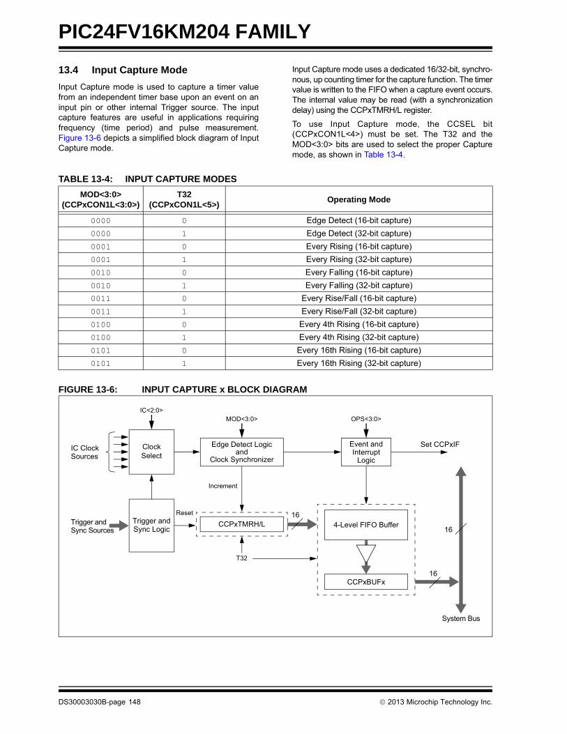
PIC24FV16KM204 FAMILY
13.4 Input Capture Mode
Input Capture mode is used to capture a timer valuefrom an independent timer base upon an event on aninput pin or other internal Trigger source. The inputcapture features are useful in applications requiringfrequency (time period) and pulse measurement.Figure 13-6 depicts a simplified block diagram of InputCapture mode.
Input Capture mode uses a dedicated 16/32-bit, synchro-nous, up counting timer for the capture function. The timervalue is written to the FIFO when a capture event occurs.The internal value may be read (with a synchronizationdelay) using the CCPxTMRH/L register.
To use Input Capture mode, the CCSEL bit(CCPxCON1L<4>) must be set. The T32 and theMOD<3:0> bits are used to select the proper Capturemode, as shown in Table 13-4.
FIGURE 13-6: INPUT CAPTURE x BLOCK DIAGRAM
TABLE 13-4: INPUT CAPTURE MODES
MOD<3:0> (CCPxCON1L<3:0>)
T32 (CCPxCON1L<5>)
Operating Mode
0000 0 Edge Detect (16-bit capture)
0000 1 Edge Detect (32-bit capture)
0001 0 Every Rising (16-bit capture)
0001 1 Every Rising (32-bit capture)
0010 0 Every Falling (16-bit capture)
0010 1 Every Falling (32-bit capture)
0011 0 Every Rise/Fall (16-bit capture)
0011 1 Every Rise/Fall (32-bit capture)
0100 0 Every 4th Rising (16-bit capture)
0100 1 Every 4th Rising (32-bit capture)
0101 0 Every 16th Rising (16-bit capture)
0101 1 Every 16th Rising (32-bit capture)
CCPxBUFx
4-Level FIFO Buffer
MOD<3:0>
Set CCPxIF
OPS<3:0>
InterruptLogic
System Bus
Event and
Trigger andSync Logic
ClockSelect
IC ClockSources
Trigger andSync Sources
IC<2:0>
16
16
16CCPxTMRH/L
Increment
Reset
T32
Edge Detect Logicand
Clock Synchronizer
DS30003030B-page 148 2013 Microchip Technology Inc.
PIC24FV16KM204 FAMILY
13.5 Auxiliary Output
The MCCPx and SCCPx modules have an auxiliary(secondary) output that provides other peripheralsaccess to internal module signals. The auxiliary outputis intended to connect to other MCCP or SCCPmodules, or other digital peripherals, to provide thesetypes of functions:
• Time Base Synchronization
• Peripheral Trigger and Clock Inputs
• Signal Gating
The type of output signal is selected using theAUXOUT<1:0> control bits (CCPxCON2H<4:3>). Thetype of output signal is also dependent on the moduleoperating mode.
On the PIC24FV16KM204 family of devices, only theCTMU discharge trigger has access to the auxiliaryoutput signal.
TABLE 13-5: AUXILIARY OUTPUT
AUXOUT<1:0> CCSEL MOD<3:0> Comments Signal Description
00 x xxxx Auxiliary output disabled No Output
01 0 0000 Time Base modes Time Base Period Reset or Rollover
10 Special Event Trigger Output
11 No Output
01 0 0001through1111
Output Compare modes Time Base Period Reset or Rollover
10 Output Compare Event Signal
11 Output Compare Signal
01 1 xxxx Input Capture modes Time Base Period Reset or Rollover
10 Reflects the Value of the ICDIS bit
11 Input Capture Event Signal
2013 Microchip Technology Inc. DS30003030B-page 149
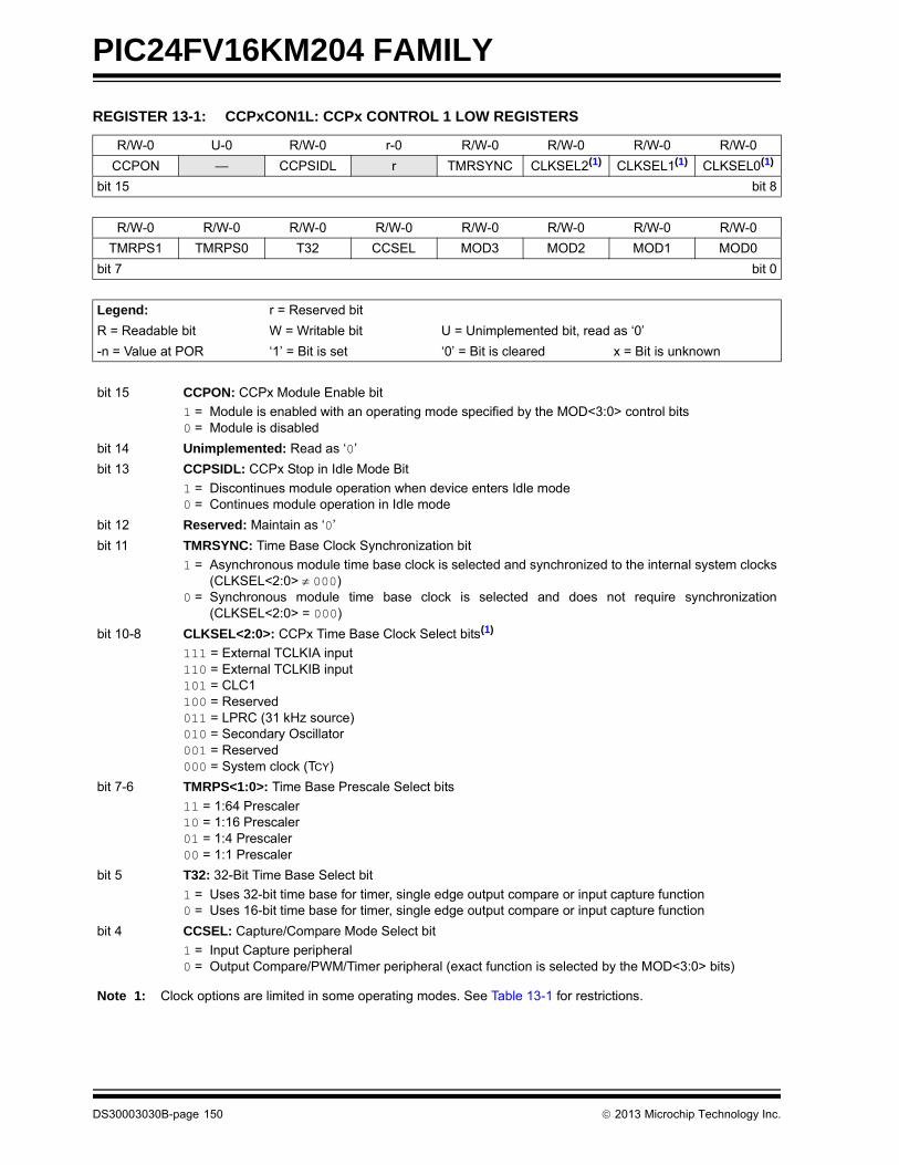
PIC24FV16KM204 FAMILY
REGISTER 13-1: CCPxCON1L: CCPx CONTROL 1 LOW REGISTERS
R/W-0 U-0 R/W-0 r-0 R/W-0 R/W-0 R/W-0 R/W-0
CCPON — CCPSIDL r TMRSYNC CLKSEL2(1) CLKSEL1(1) CLKSEL0(1)
bit 15 bit 8
R/W-0 R/W-0 R/W-0 R/W-0 R/W-0 R/W-0 R/W-0 R/W-0
TMRPS1 TMRPS0 T32 CCSEL MOD3 MOD2 MOD1 MOD0
bit 7 bit 0
Legend: r = Reserved bit
R = Readable bit W = Writable bit U = Unimplemented bit, read as ‘0’
-n = Value at POR ‘1’ = Bit is set ‘0’ = Bit is cleared x = Bit is unknown
bit 15 CCPON: CCPx Module Enable bit
1 = Module is enabled with an operating mode specified by the MOD<3:0> control bits0 = Module is disabled
bit 14 Unimplemented: Read as ‘0’
bit 13 CCPSIDL: CCPx Stop in Idle Mode Bit
1 = Discontinues module operation when device enters Idle mode0 = Continues module operation in Idle mode
bit 12 Reserved: Maintain as ‘0’
bit 11 TMRSYNC: Time Base Clock Synchronization bit
1 = Asynchronous module time base clock is selected and synchronized to the internal system clocks(CLKSEL<2:0> 000)
0 = Synchronous module time base clock is selected and does not require synchronization(CLKSEL<2:0> = 000)
bit 10-8 CLKSEL<2:0>: CCPx Time Base Clock Select bits(1)
111 = External TCLKIA input110 = External TCLKIB input101 = CLC1100 = Reserved011 = LPRC (31 kHz source)010 = Secondary Oscillator001 = Reserved000 = System clock (TCY)
bit 7-6 TMRPS<1:0>: Time Base Prescale Select bits
11 = 1:64 Prescaler10 = 1:16 Prescaler01 = 1:4 Prescaler00 = 1:1 Prescaler
bit 5 T32: 32-Bit Time Base Select bit
1 = Uses 32-bit time base for timer, single edge output compare or input capture function0 = Uses 16-bit time base for timer, single edge output compare or input capture function
bit 4 CCSEL: Capture/Compare Mode Select bit
1 = Input Capture peripheral0 = Output Compare/PWM/Timer peripheral (exact function is selected by the MOD<3:0> bits)
Note 1: Clock options are limited in some operating modes. See Table 13-1 for restrictions.
DS30003030B-page 150 2013 Microchip Technology Inc.

PIC24FV16KM204 FAMILY
bit 3-0 MOD<3:0>: CCPx Mode Select bits
For CCSEL = 1 (Input Capture modes):1xxx = Reserved011x = Reserved0101 = Capture every 16th rising edge0100 = Capture every 4th rising edge0011 = Capture every rising and falling edge0010 = Capture every falling edge0001 = Capture every rising edge0000 = Capture every rising and falling edge (Edge Detect mode)
For CCSEL = 0 (Output Compare/Timer modes):1111 = External Input mode: Pulse generator is disabled, source is selected by ICS<2:0>1110 = Reserved110x = Reserved10xx = Reserved0111 = Variable Frequency Pulse mode0110 = Center-Aligned Pulse Compare mode, buffered0101 = Dual Edge Compare mode, buffered0100 = Dual Edge Compare mode0011 = 16-Bit/32-Bit Single Edge mode, toggle output on compare match0010 = 16-Bit/32-Bit Single Edge mode, drive output low on compare match0001 = 16-Bit/32-Bit Single Edge mode, drive output high on compare match0000 = 16-Bit/32-Bit Timer mode, output functions are disabled
REGISTER 13-1: CCPxCON1L: CCPx CONTROL 1 LOW REGISTERS (CONTINUED)
Note 1: Clock options are limited in some operating modes. See Table 13-1 for restrictions.
2013 Microchip Technology Inc. DS30003030B-page 151
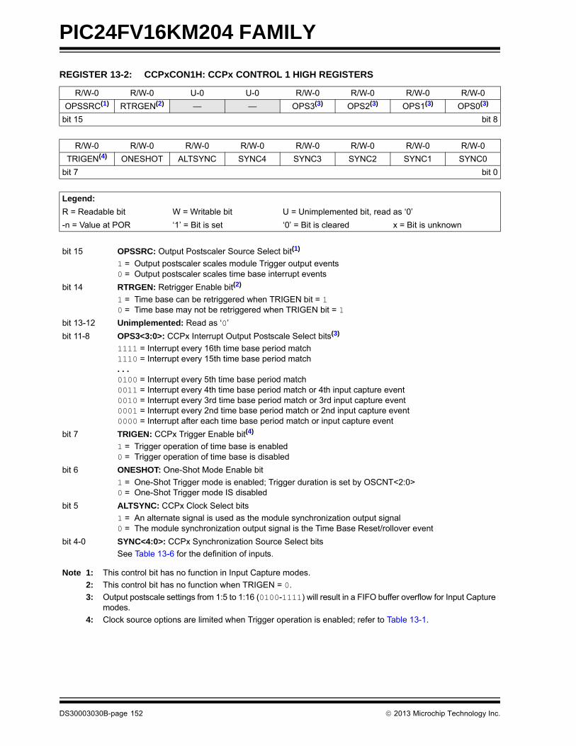
PIC24FV16KM204 FAMILY
REGISTER 13-2: CCPxCON1H: CCPx CONTROL 1 HIGH REGISTERS
R/W-0 R/W-0 U-0 U-0 R/W-0 R/W-0 R/W-0 R/W-0
OPSSRC(1) RTRGEN(2) — — OPS3(3) OPS2(3) OPS1(3) OPS0(3)
bit 15 bit 8
R/W-0 R/W-0 R/W-0 R/W-0 R/W-0 R/W-0 R/W-0 R/W-0
TRIGEN(4) ONESHOT ALTSYNC SYNC4 SYNC3 SYNC2 SYNC1 SYNC0
bit 7 bit 0
Legend:
R = Readable bit W = Writable bit U = Unimplemented bit, read as ‘0’
-n = Value at POR ‘1’ = Bit is set ‘0’ = Bit is cleared x = Bit is unknown
bit 15 OPSSRC: Output Postscaler Source Select bit(1)
1 = Output postscaler scales module Trigger output events0 = Output postscaler scales time base interrupt events
bit 14 RTRGEN: Retrigger Enable bit(2)
1 = Time base can be retriggered when TRIGEN bit = 10 = Time base may not be retriggered when TRIGEN bit = 1
bit 13-12 Unimplemented: Read as ‘0’
bit 11-8 OPS3<3:0>: CCPx Interrupt Output Postscale Select bits(3)
1111 = Interrupt every 16th time base period match1110 = Interrupt every 15th time base period match. . .0100 = Interrupt every 5th time base period match0011 = Interrupt every 4th time base period match or 4th input capture event0010 = Interrupt every 3rd time base period match or 3rd input capture event0001 = Interrupt every 2nd time base period match or 2nd input capture event0000 = Interrupt after each time base period match or input capture event
bit 7 TRIGEN: CCPx Trigger Enable bit(4)
1 = Trigger operation of time base is enabled0 = Trigger operation of time base is disabled
bit 6 ONESHOT: One-Shot Mode Enable bit
1 = One-Shot Trigger mode is enabled; Trigger duration is set by OSCNT<2:0>0 = One-Shot Trigger mode IS disabled
bit 5 ALTSYNC: CCPx Clock Select bits
1 = An alternate signal is used as the module synchronization output signal 0 = The module synchronization output signal is the Time Base Reset/rollover event
bit 4-0 SYNC<4:0>: CCPx Synchronization Source Select bits
See Table 13-6 for the definition of inputs.
Note 1: This control bit has no function in Input Capture modes.
2: This control bit has no function when TRIGEN = 0.
3: Output postscale settings from 1:5 to 1:16 (0100-1111) will result in a FIFO buffer overflow for Input Capture modes.
4: Clock source options are limited when Trigger operation is enabled; refer to Table 13-1.
DS30003030B-page 152 2013 Microchip Technology Inc.

PIC24FV16KM204 FAMILY
TABLE 13-6: SYNCHRONIZATION SOURCES
SYNC<4:0> Synchronization Source
00000 None; Timer with Rollover on CCPxPR Match or FFFFh
00001 MCCP1 or SCCP1 Sync Output
00010 MCCP2 or SCCP2 Sync Output
00011 MCCP3 or SCCP3 Sync Output
00100 MCCP4 or SCCP4 Sync Output
00101 MCCP5 or SCCP5 Sync Output
00110 to 01010 Unused
01011 Timer1 Sync Output(1)
01100 to 10000 Unused
10001 CLC1 Output(1)
10010 CLC2 Output(1)
10011 to 11010 Unused
11011 A/D(1)
11110 Unused
11111 None; Timer with Auto-Rollover (FFFFh → 0000h)
Note 1: These sources are only available when the source module is being used in a Synchronous mode.
2013 Microchip Technology Inc. DS30003030B-page 153
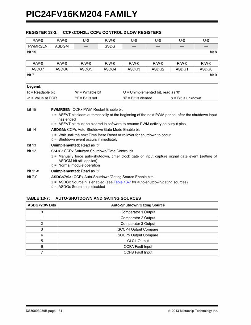
PIC24FV16KM204 FAMILY
TABLE 13-7: AUTO-SHUTDOWN AND GATING SOURCES
REGISTER 13-3: CCPxCON2L: CCPx CONTROL 2 LOW REGISTERS
R/W-0 R/W-0 U-0 R/W-0 U-0 U-0 U-0 U-0
PWMRSEN ASDGM — SSDG — — — —
bit 15 bit 8
R/W-0 R/W-0 R/W-0 R/W-0 R/W-0 R/W-0 R/W-0 R/W-0
ASDG7 ASDG6 ASDG5 ASDG4 ASDG3 ASDG2 ASDG1 ASDG0
bit 7 bit 0
Legend:
R = Readable bit W = Writable bit U = Unimplemented bit, read as ‘0’
-n = Value at POR ‘1’ = Bit is set ‘0’ = Bit is cleared x = Bit is unknown
bit 15 PWMRSEN: CCPx PWM Restart Enable bit
1 = ASEVT bit clears automatically at the beginning of the next PWM period, after the shutdown inputhas ended
0 = ASEVT bit must be cleared in software to resume PWM activity on output pins
bit 14 ASDGM: CCPx Auto-Shutdown Gate Mode Enable bit
1 = Wait until the next Time Base Reset or rollover for shutdown to occur0 = Shutdown event occurs immediately
bit 13 Unimplemented: Read as ‘0’
bit 12 SSDG: CCPx Software Shutdown/Gate Control bit
1 = Manually force auto-shutdown, timer clock gate or input capture signal gate event (setting ofASDGM bit still applies)
0 = Normal module operation
bit 11-8 Unimplemented: Read as ‘0’
bit 7-0 ASDG<7:0>: CCPx Auto-Shutdown/Gating Source Enable bits
1 = ASDGx Source n is enabled (see Table 13-7 for auto-shutdown/gating sources)0 = ASDGx Source n is disabled
ASDG<7:0> Bits Auto-Shutdown/Gating Source
0 Comparator 1 Output
1 Comparator 2 Output
2 Comparator 3 Output
3 SCCP4 Output Compare
4 SCCP5 Output Compare
5 CLC1 Output
6 OCFA Fault Input
7 OCFB Fault Input
DS30003030B-page 154 2013 Microchip Technology Inc.

PIC24FV16KM204 FAMILY
REGISTER 13-4: CCPxCON2H: CCPx CONTROL 2 HIGH REGISTERS
R/W-0 U-0 R/W-0 R/W-0 R/W-0 R/W-0 R/W-0 R/W-0
OENSYNC — OCFEN(1) OCEEN(1) OCDEN(1) OCCEN(1) OCBEN(1) OCAEN
bit 15 bit 8
R/W-0 R/W-0 U-0 R/W-0 R/W-0 R/W-0 R/W-0 R/W-0
ICGSM1 ICGSM0 — AUXOUT1 AUXOUT0 ICS2 ICS1 ICS0
bit 7 bit 0
Legend:
R = Readable bit W = Writable bit U = Unimplemented bit, read as ‘0’
-n = Value at POR ‘1’ = Bit is set ‘0’ = Bit is cleared x = Bit is unknown
bit 15 OENSYNC: Output Enable Synchronization bit
1 = Update by output enable bits occurs on the next Time Base Reset or rollover0 = Update by output enable bits occurs immediately
bit 14 Unimplemented: Read as ‘0’
bit 13-8 OC<F:A>EN: Output Enable/Steering Control bits(1)
1 = OCx pin is controlled by the CCPx module and produces an output compare or PWM signal0 = OCx pin is not controlled by the CCPx module; the pin is available to the port logic or another
peripheral multiplexed on the pin
bit 7-6 ICGSM<1:0>: Input Capture Gating Source Mode Control bits
11 = Reserved10 = One-Shot mode: Falling edge from gating source disables future capture events (ICDIS = 1)01 = One-Shot mode: Rising edge from gating source enables future capture events (ICDIS = 0)00 = Level-Sensitive mode: A high level from gating source will enable future capture events; a low
level will disable future capture events
bit 5 Unimplemented: Read as ‘0’
bit 4-3 AUXOUT<1:0>: Auxiliary Output Signal on Event Selection bits
11 = Input capture or output compare event; no signal in Timer mode10 = Signal output is defined by module operating mode (see Table 13-5)01 = Time base rollover event (all modes)00 = Disabled
bit 2-0 ICS<2:0>: Input Capture Source Select bits
111 = Unused110 = CLC2 output101 = CLC1 output100 = Unused011 = Comparator 3 output010 = Comparator 2 output001 = Comparator 1 output000 = Input Capture x (ICx) I/O pin
Note 1: OCFEN through OCBEN (bits<13:9>) are implemented in MCCPx modules only.
2013 Microchip Technology Inc. DS30003030B-page 155

PIC24FV16KM204 FAMILY
REGISTER 13-5: CCPxCON3L: CCPx CONTROL 3 LOW REGISTERS (1)
U-0 U-0 U-0 U-0 U-0 U-0 U-0 U-0
— — — — — — — —
bit 15 bit 8
U-0 U-0 R/W-0 R/W-0 R/W-0 R/W-0 R/W-0 R/W-0
— — DT5 DT4 DT3 DT2 DT1 DT0
bit 7 bit 0
Legend:
R = Readable bit W = Writable bit U = Unimplemented bit, read as ‘0’
-n = Value at POR ‘1’ = Bit is set ‘0’ = Bit is cleared x = Bit is unknown
bit 15-6 Unimplemented: Read as ‘0’
bit 5-0 DT<5:0>: CCPx Dead-Time Select bits
111111 = Insert 63 dead-time delay periods between complementary output signals111110 = Insert 62 dead-time delay periods between complementary output signals. . .000010 = Insert 2 dead-time delay periods between complementary output signals000001 = Insert 1 dead-time delay period between complementary output signals000000 = Dead-time logic is disabled
Note 1: This register is implemented in MCCPx modules only.
DS30003030B-page 156 2013 Microchip Technology Inc.
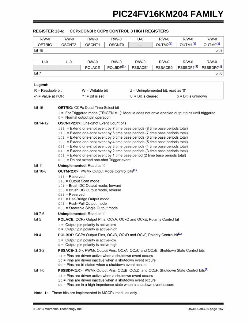
PIC24FV16KM204 FAMILY
REGISTER 13-6: CCPxCON3H: CCPx CONTROL 3 HIGH REGISTERS
R/W-0 R/W-0 R/W-0 R/W-0 U-0 R/W-0 R/W-0 R/W-0
OETRIG OSCNT2 OSCNT1 OSCNT0 — OUTM2(1) OUTM1(1) OUTM0(1)
bit 15 bit 8
U-0 U-0 R/W-0 R/W-0 R/W-0 R/W-0 R/W-0 R/W-0
— — POLACE POLBDF(1) PSSACE1 PSSACE0 PSSBDF1(1) PSSBDF0(1)
bit 7 bit 0
Legend:
R = Readable bit W = Writable bit U = Unimplemented bit, read as ‘0’
-n = Value at POR ‘1’ = Bit is set ‘0’ = Bit is cleared x = Bit is unknown
bit 15 OETRIG: CCPx Dead-Time Select bit
1 = For Triggered mode (TRIGEN = 1): Module does not drive enabled output pins until triggered0 = Normal output pin operation
bit 14-12 OSCNT<2:0>: One-Shot Event Count bits
111 = Extend one-shot event by 7 time base periods (8 time base periods total)110 = Extend one-shot event by 6 time base periods (7 time base periods total)101 = Extend one-shot event by 5 time base periods (6 time base periods total)100 = Extend one-shot event by 4 time base periods (5 time base periods total)011 = Extend one-shot event by 3 time base periods (4 time base periods total)010 = Extend one-shot event by 2 time base periods (3 time base periods total)001 = Extend one-shot event by 1 time base period (2 time base periods total)000 = Do not extend one-shot Trigger event
bit 11 Unimplemented: Read as ‘0’
bit 10-8 OUTM<2:0>: PWMx Output Mode Control bits(1)
111 = Reserved110 = Output Scan mode101 = Brush DC Output mode, forward100 = Brush DC Output mode, reverse011 = Reserved010 = Half-Bridge Output mode001 = Push-Pull Output mode000 = Steerable Single Output mode
bit 7-6 Unimplemented: Read as ‘0’
bit 5 POLACE: CCPx Output Pins, OCxA, OCxC and OCxE, Polarity Control bit
1 = Output pin polarity is active-low0 = Output pin polarity is active-high
bit 4 POLBDF: CCPx Output Pins, OCxB, OCxD and OCxF, Polarity Control bit(1)
1 = Output pin polarity is active-low0 = Output pin polarity is active-high
bit 3-2 PSSACE<1:0>: PWMx Output Pins, OCxA, OCxC and OCxE, Shutdown State Control bits
11 = Pins are driven active when a shutdown event occurs10 = Pins are driven inactive when a shutdown event occurs0x = Pins are tri-stated when a shutdown event occurs
bit 1-0 PSSBDF<1:0>: PWMx Output Pins, OCxB, OCxD, and OCxF, Shutdown State Control bits(1)
11 = Pins are driven active when a shutdown event occurs10 = Pins are driven inactive when a shutdown event occurs0x = Pins are in a high-impedance state when a shutdown event occurs
Note 1: These bits are implemented in MCCPx modules only.
2013 Microchip Technology Inc. DS30003030B-page 157

PIC24FV16KM204 FAMILY
REGISTER 13-7: CCPxSTATL: CCPx STATUS REGISTER
U-0 U-0 U-0 U-0 U-0 U-0 U-0 U-0
— — — — — — — —
bit 15 bit 8
R-0 W1-0 W1-0 R/C-0 R/C-0 R/C-0 R/C-0 R/C-0
CCPTRIG TRSET TRCLR ASEVT SCEVT ICDIS ICOV ICBNE
bit 7 bit 0
Legend: C = Clearable bit
R = Readable bit W1 = Write ‘1’ only U = Unimplemented bit, read as ‘0’
-n = Value at POR ‘1’ = Bit is set ‘0’ = Bit is cleared x = Bit is unknown
bit 15-8 Unimplemented: Read as ‘0’
bit 7 CCPTRIG: CCPx Trigger Status bit
1 = Timer has been triggered and is running0 = Timer has not been triggered and is held in Reset
bit 6 TRSET: CCPx Trigger Set Request bit
Write ‘1’ to this location to trigger the timer when TRIGEN = 1 (location always reads as ‘0’).
bit 5 TRCLR: CCPx Trigger Clear Request bit
Write ‘1’ to this location to cancel the timer Trigger when TRIGEN = 1 (location always reads as ‘0’).
bit 4 ASEVT: CCPx Auto-Shutdown Event Status/Control bit
1 = A shutdown event is in progress; CCPx outputs are in the shutdown state0 = CCPx outputs operate normally
bit 3 SCEVT: Single Edge Compare Event Status bit
1 = A single edge compare event has occurred0 = A single edge compare event has not occurred
bit 2 ICDIS: Input Capture x Disable bit
1 = Event on Input Capture x pin (ICx) does not generate a capture event0 = Event on Input Capture x pin will generate a capture event
bit 1 ICOV: Input Capture x Buffer Overflow Status bit
1 = The Input Capture x FIFO buffer has overflowed0 = The Input Capture x FIFO buffer has not overflowed
bit 0 ICBNE: Input Capture x Buffer Status bit
1 = Input Capture x buffer has data available0 = Input Capture x buffer is empty
DS30003030B-page 158 2013 Microchip Technology Inc.

PIC24FV16KM204 FAMILY
14.0 MASTER SYNCHRONOUS SERIAL PORT (MSSP)
The Master Synchronous Serial Port (MSSP) module isan 8-bit serial interface, useful for communicating withother peripheral or microcontroller devices. Theseperipheral devices may be serial EEPROMs, Shift reg-isters, display drivers, A/D Converters, etc. The MSSPmodule can operate in one of two modes:
• Serial Peripheral Interface (SPI)
• Inter-Integrated Circuit (I2C™)
- Full Master mode
- Slave mode (with general address call)
The SPI interface supports these modes in hardware:
• Master mode
• Slave mode
• Daisy-Chaining Operation in Slave mode
• Synchronized Slave Operation
The I2C interface supports the following modes inhardware:
• Master mode
• Multi-Master mode
• Slave mode with 10-Bit and 7-Bit Addressing and Address Masking
• Byte NACKing
• Selectable Address and Data Hold, and Interrupt Masking
14.1 I/O Pin Configuration for SPI
In SPI Master mode, the MSSP module will assert con-trol over any pins associated with the SDOx and SCKxoutputs. This does not automatically disable other digi-tal functions associated with the pin and may result inthe module driving the digital I/O port inputs. To preventthis, the MSSP module outputs must be disconnectedfrom their output pins while the module is in SPI Mastermode. While disabling the module temporarily may bean option, it may not be a practical solution in allapplications.
The SDOx and SCKx outputs for the module can beselectively disabled by using the SDOxDIS andSCKxDIS bits in the PADCFG1 register (Register 14-10).Setting the bit disconnects the corresponding output for aparticular module from its assigned pin.
Note: This data sheet summarizes the features ofthis group of PIC24F devices. It is notintended to be a comprehensive referencesource. For more information on MSSP,refer to the “PIC24F Family ReferenceManual”.
2013 Microchip Technology Inc. DS30003030B-page 159

PIC24FV16KM204 FAMILY
FIGURE 14-1: MSSPx BLOCK DIAGRAM (SPI MODE)
FIGURE 14-2: SPI MASTER/SLAVE CONNECTION
( )
Read Write
Internal Data Bus
SSPM<3:0>
bit 0Shift Clock
SSx Control Enable
EdgeSelect
Clock Select
TMR2 Output
TOSCPrescaler4, 16, 64
2EdgeSelect
2
4
Data to TX/RX in SSPxSRTRISx bit
2SMP:CKE
SDOx
SDIx
SSx
SCKx
Note: Refer to the device data sheet for pin multiplexing.
SSPxADD<7:0>
7
SSPxBUF
SSPxSR
BaudRate
Generator
Serial Input Buffer(SSPxBUF)
Shift Register(SSPxSR)
MSb LSb
SDOx
SDIx
PROCESSOR 1SCKx
SPI Master SSPM<3:0> = 00xx
Serial Input Buffer(SSPxBUF)
Shift Register(SSPxSR)
LSbMSb
SDIx
SDOx
PROCESSOR 2SCKx
SPI Slave SSPM<3:0> = 010x
Serial Clock
DS30003030B-page 160 2013 Microchip Technology Inc.

PIC24FV16KM204 FAMILY
FIGURE 14-3: MSSPx BLOCK DIAGRAM (I2C™ MODE)
FIGURE 14-4: MSSPx BLOCK DIAGRAM (I2C™ MASTER MODE)
Match Detect
SSPxADD
Internal Data Bus
Address Match
Set/Reset S, P bits
ShiftClock
MSb LSb
Note: Only port I/O names are shown in this diagram. Refer to the text for a full list of multiplexed functions.
SCLx
SDAx
Start andStop bit Detect
Read Write
SSPxBUF
SSPxSR
Address Mask
Start bit, Stop bit,
Internal Data Bus
Set/Reset S, P (SSPxSTAT), WCOL
ShiftClock
MSb LSb
SDAx
AcknowledgeGenerate
Stop bit DetectWrite Collision Detect
Clock ArbitrationState Counter forEnd of XMIT/RCV
SCLx
SCLx In
Bus Collision
SDAx In
RCV Enable
Clock Cntl
Clock Arbitrate/WCOL Detect(hold off clock source)
SSPxADD<6:0>
Baud
Set SSPxIF, BCLxIFReset ACKSTAT, PEN
RateGenerator
SSPM<3:0>
Start bit Detect
SSPxSR
SSPxBUF
Read Write
2013 Microchip Technology Inc. DS30003030B-page 161

PIC24FV16KM204 FAMILY
REGISTER 14-1: SSPxSTAT: MSSPx STATUS REGISTER (SPI MODE)
U-0 U-0 U-0 U-0 U-0 U-0 U-0 U-0
— — — — — — — —
bit 15 bit 8
R/W-0 R/W-0 R-0 R-0 R-0 R-0 R-0 R-0
SMP CKE(1) D/A P S R/W UA BF
bit 7 bit 0
Legend:
R = Readable bit W = Writable bit U = Unimplemented bit, read as ‘0’
-n = Value at POR ‘1’ = Bit is set ‘0’ = Bit is cleared x = Bit is unknown
bit 15-8 Unimplemented: Read as ‘0’
bit 7 SMP: Sample bit
SPI Master mode:1 = Input data is sampled at the end of data output time0 = Input data is sampled at the middle of data output time
SPI Slave mode:SMP must be cleared when SPI is used in Slave mode.
bit 6 CKE: SPI Clock Select bit(1)
1 = Transmit occurs on transition from active to Idle clock state0 = Transmit occurs on transition from Idle to active clock state
bit 5 D/A: Data/Address bit
Used in I2C™ mode only.
bit 4 P: Stop bit
Used in I2C mode only. This bit is cleared when the MSSPx module is disabled; SSPEN bit is cleared.
bit 3 S: Start bit
Used in I2C mode only.
bit 2 R/W: Read/Write Information bit
Used in I2C mode only.
bit 1 UA: Update Address bit
Used in I2C mode only.
bit 0 BF: Buffer Full Status bit
1 = Receive is complete, SSPxBUF is full 0 = Receive is not complete, SSPxBUF is empty
Note 1: Polarity of clock state is set by the CKP bit (SSPxCON1<4>).
DS30003030B-page 162 2013 Microchip Technology Inc.
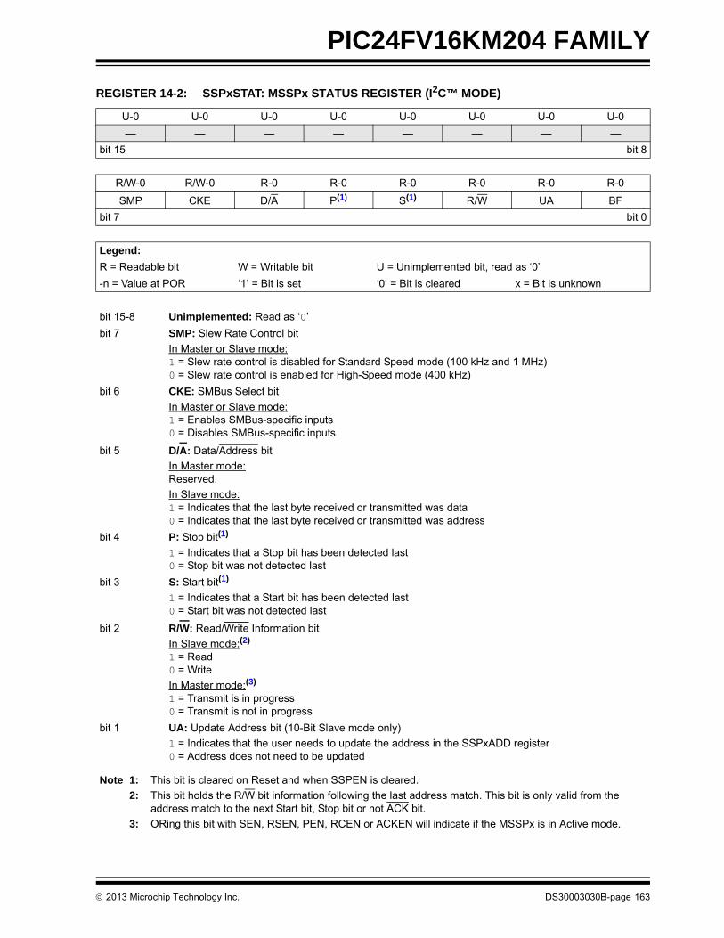
PIC24FV16KM204 FAMILY
REGISTER 14-2: SSPxSTAT: MSSPx STATUS REGISTER (I2C™ MODE)
U-0 U-0 U-0 U-0 U-0 U-0 U-0 U-0
— — — — — — — —
bit 15 bit 8
R/W-0 R/W-0 R-0 R-0 R-0 R-0 R-0 R-0
SMP CKE D/A P(1) S(1) R/W UA BF
bit 7 bit 0
Legend:
R = Readable bit W = Writable bit U = Unimplemented bit, read as ‘0’
-n = Value at POR ‘1’ = Bit is set ‘0’ = Bit is cleared x = Bit is unknown
bit 15-8 Unimplemented: Read as ‘0’
bit 7 SMP: Slew Rate Control bit
In Master or Slave mode: 1 = Slew rate control is disabled for Standard Speed mode (100 kHz and 1 MHz) 0 = Slew rate control is enabled for High-Speed mode (400 kHz)
bit 6 CKE: SMBus Select bit
In Master or Slave mode:1 = Enables SMBus-specific inputs 0 = Disables SMBus-specific inputs
bit 5 D/A: Data/Address bit
In Master mode:Reserved.
In Slave mode:1 = Indicates that the last byte received or transmitted was data0 = Indicates that the last byte received or transmitted was address
bit 4 P: Stop bit(1)
1 = Indicates that a Stop bit has been detected last0 = Stop bit was not detected last
bit 3 S: Start bit(1)
1 = Indicates that a Start bit has been detected last0 = Start bit was not detected last
bit 2 R/W: Read/Write Information bit
In Slave mode:(2)
1 = Read0 = Write
In Master mode:(3)
1 = Transmit is in progress0 = Transmit is not in progress
bit 1 UA: Update Address bit (10-Bit Slave mode only)
1 = Indicates that the user needs to update the address in the SSPxADD register 0 = Address does not need to be updated
Note 1: This bit is cleared on Reset and when SSPEN is cleared.
2: This bit holds the R/W bit information following the last address match. This bit is only valid from the address match to the next Start bit, Stop bit or not ACK bit.
3: ORing this bit with SEN, RSEN, PEN, RCEN or ACKEN will indicate if the MSSPx is in Active mode.
2013 Microchip Technology Inc. DS30003030B-page 163

PIC24FV16KM204 FAMILY
bit 0 BF: Buffer Full Status bit
In Transmit mode: 1 = Transmit is in progress, SSPxBUF is full 0 = Transmit is complete, SSPxBUF is empty
In Receive mode:1 = SSPxBUF is full (does not include the ACK and Stop bits)0 = SSPxBUF is empty (does not include the ACK and Stop bits)
REGISTER 14-2: SSPxSTAT: MSSPx STATUS REGISTER (I2C™ MODE) (CONTINUED)
Note 1: This bit is cleared on Reset and when SSPEN is cleared.
2: This bit holds the R/W bit information following the last address match. This bit is only valid from the address match to the next Start bit, Stop bit or not ACK bit.
3: ORing this bit with SEN, RSEN, PEN, RCEN or ACKEN will indicate if the MSSPx is in Active mode.
DS30003030B-page 164 2013 Microchip Technology Inc.

PIC24FV16KM204 FAMILY
REGISTER 14-3: SSPxCON1: MSSPx CONTROL REGISTER 1 (SPI MODE)
U-0 U-0 U-0 U-0 U-0 U-0 U-0 U-0
— — — — — — — —
bit 15 bit 8
R/W-0 R/W-0 R/W-0 R/W-0 R/W-0 R/W-0 R/W-0 R/W-0
WCOL SSPOV(1) SSPEN(2) CKP SSPM3(3) SSPM2(3) SSPM1(3) SSPM0(3)
bit 7 bit 0
Legend:
R = Readable bit W = Writable bit U = Unimplemented bit, read as ‘0’
-n = Value at POR ‘1’ = Bit is set ‘0’ = Bit is cleared x = Bit is unknown
bit 15-8 Unimplemented: Read as ‘0’
bit 7 WCOL: Write Collision Detect bit
1 = The SSPxBUF register is written while it is still transmitting the previous word (must be cleared insoftware)
0 = No collision
bit 6 SSPOV: Master Synchronous Serial Port Receive Overflow Indicator bit(1)
SPI Slave mode: 1 = A new byte is received while the SSPxBUF register is still holding the previous data. In case of over-
flow, the data in SSPxSR is lost. Overflow can only occur in Slave mode. The user must read theSSPxBUF, even if only transmitting data, to avoid setting overflow (must be cleared in software).
0 = No overflow
bit 5 SSPEN: Master Synchronous Serial Port Enable bit(2)
1 = Enables the serial port and configures SCKx, SDOx, SDIx and SSx as serial port pins 0 = Disables the serial port and configures these pins as I/O port pins
bit 4 CKP: Clock Polarity Select bit
1 = Idle state for clock is a high level 0 = Idle state for clock is a low level
bit 3-0 SSPM<3:0>: Master Synchronous Serial Port Mode Select bits(3)
1010 = SPI Master mode, Clock = FOSC/(2 * ([SSPxADD] + 1))0101 = SPI Slave mode, Clock = SCKx pin; SSx pin control is disabled, SSx can be used as an I/O pin 0100 = SPI Slave mode, Clock = SCKx pin; SSx pin control is enabled0011 = SPI Master mode, Clock = TMR2 output/2 0010 = SPI Master mode, Clock = FOSC/32 0001 = SPI Master mode, Clock = FOSC/8 0000 = SPI Master mode, Clock = FOSC/2
Note 1: In Master mode, the overflow bit is not set since each new reception (and transmission) is initiated by writing to the SSPxBUF register.
2: When enabled, these pins must be properly configured as inputs or outputs.
3: Bit combinations not specifically listed here are either reserved or implemented in I2C™ mode only.
2013 Microchip Technology Inc. DS30003030B-page 165

PIC24FV16KM204 FAMILY
REGISTER 14-4: SSPxCON1: MSSPx CONTROL REGISTER 1 (I2C™ MODE)
U-0 U-0 U-0 U-0 U-0 U-0 U-0 U-0
— — — — — — — —
bit 15 bit 8
R/W-0 R/W-0 R/W-0 R/W-0 R/W-0 R/W-0 R/W-0 R/W-0
WCOL SSPOV SSPEN(1) CKP SSPM3(2) SSPM2(2) SSPM1(2) SSPM0(2)
bit 7 bit 0
Legend:
R = Readable bit W = Writable bit U = Unimplemented bit, read as ‘0’
-n = Value at POR ‘1’ = Bit is set ‘0’ = Bit is cleared x = Bit is unknown
bit 15-8 Unimplemented: Read as ‘0’
bit 7 WCOL: Write Collision Detect bit
In Master Transmit mode:1 = A write to the SSPxBUF register was attempted while the I2C conditions were not valid for a
transmission to be started (must be cleared in software)0 = No collision
In Slave Transmit mode:1 = The SSPxBUF register is written while it is still transmitting the previous word (must be cleared in
software)0 = No collision
In Receive mode (Master or Slave modes):This is a “don’t care” bit.
bit 6 SSPOV: Master Synchronous Serial Port Receive Overflow Indicator bit
In Receive mode:1 = A byte is received while the SSPxBUF register is still holding the previous byte (must be cleared in
software)0 = No overflow
In Transmit mode: This is a “don’t care” bit in Transmit mode.
bit 5 SSPEN: Master Synchronous Serial Port Enable bit(1)
1 = Enables the serial port and configures the SDAx and SCLx pins as the serial port pins 0 = Disables the serial port and configures these pins as I/O port pins
bit 4 CKP: SCLx Release Control bit
In Slave mode:1 = Releases clock 0 = Holds clock low (clock stretch), used to ensure data setup time
In Master mode:Unused in this mode.
bit 3-0 SSPM<3:0>: Master Synchronous Serial Port Mode Select bits(2)
1111 = I2C Slave mode, 10-bit address with Start and Stop bit interrupts enabled1110 = I2C Slave mode, 7-bit address with Start and Stop bit interrupts enabled1011 = I2C Firmware Controlled Master mode (Slave Idle)1000 = I2C Master mode, Clock = FOSC/(2 * ([SSPxADD] + 1))(3)
0111 = I2C Slave mode, 10-bit address0110 = I2C Slave mode, 7-bit address
Note 1: When enabled, the SDAx and SCLx pins must be configured as inputs.
2: Bit combinations not specifically listed here are either reserved or implemented in SPI mode only.
3: SSPxADD values of 0, 1 or 2 are not supported when the Baud Rate Generator is used with I2C mode.
DS30003030B-page 166 2013 Microchip Technology Inc.

PIC24FV16KM204 FAMILY
REGISTER 14-5: SSPxCON2: MSSPx CONTROL REGISTER 2 (I2C™ MODE)
U-0 U-0 U-0 U-0 U-0 U-0 U-0 U-0
— — — — — — — —
bit 15 bit 8
R/W-0 R/W-0 R/W-0 R/W-0 R/W-0 R/W-0 R/W-0 R/W-0
GCEN ACKSTAT ACKDT(1) ACKEN(2) RCEN(2) PEN(2) RSEN(2) SEN(2)
bit 7 bit 0
Legend:
R = Readable bit W = Writable bit U = Unimplemented bit, read as ‘0’
-n = Value at POR ‘1’ = Bit is set ‘0’ = Bit is cleared x = Bit is unknown
bit 15-8 Unimplemented: Read as ‘0’
bit 7 GCEN: General Call Enable bit (Slave mode only)
1 = Enables interrupt when a general call address (0000h) is received in the SSPxSR 0 = General call address is disabled
bit 6 ACKSTAT: Acknowledge Status bit (Master Transmit mode only)
1 = Acknowledge was not received from slave 0 = Acknowledge was received from slave
bit 5 ACKDT: Acknowledge Data bit (Master Receive mode only)(1)
1 = No Acknowledge0 = Acknowledge
bit 4 ACKEN: Acknowledge Sequence Enable bit (Master mode only)(2)
1 = Initiates Acknowledge sequence on SDAx and SCLx pins and transmits ACKDT data bit;automatically cleared by hardware
0 = Acknowledge sequence is Idle
bit 3 RCEN: Receive Enable bit (Master Receive mode only)(2)
1 = Enables Receive mode for I2C 0 = Receive is Idle
bit 2 PEN: Stop Condition Enable bit (Master mode only)(2)
1 = Initiates Stop condition on SDAx and SCLx pins; automatically cleared by hardware0 = Stop condition is Idle
bit 1 RSEN: Repeated Start Condition Enable bit (Master mode only)(2)
1 = Initiates Repeated Start condition on SDAx and SCLx pins; automatically cleared by hardware0 = Repeated Start condition is Idle
bit 0 SEN: Start Condition Enable bit(2)
Master Mode:
1 = Initiates Start condition on SDAx and SCLx pins; automatically cleared by hardware0 = Start condition is IdleSlave Mode:
1 = Clock stretching is enabled for both slave transmit and slave receive (stretch is enabled)0 = Clock stretching is disabled
Note 1: The value that will be transmitted when the user initiates an Acknowledge sequence at the end of a receive.
2: If the I2C module is active, these bits may not be set (no spooling) and the SSPxBUF may not be written (or writes to the SSPxBUF are disabled).
2013 Microchip Technology Inc. DS30003030B-page 167

PIC24FV16KM204 FAMILY
REGISTER 14-6: SSPxCON3: MSSPx CONTROL REGISTER 3 (SPI MODE)
U-0 U-0 U-0 U-0 U-0 U-0 U-0 U-0
— — — — — — — —
bit 15 bit 8
R-0 R/W-0 R/W-0 R/W-0 R/W-0 R/W-0 R/W-0 R/W-0
ACKTIM PCIE SCIE BOEN(1) SDAHT SBCDE AHEN DHEN
bit 7 bit 0
Legend:
R = Readable bit W = Writable bit U = Unimplemented bit, read as ‘0’
-n = Value at POR ‘1’ = Bit is set ‘0’ = Bit is cleared x = Bit is unknown
bit 15-8 Unimplemented: Read as ‘0’
bit 7 ACKTIM: Acknowledge Time Status bit (I2C™ mode only)
Unused in SPI mode.
bit 6 PCIE: Stop Condition Interrupt Enable bit (I2C mode only)
Unused in SPI mode.
bit 5 SCIE: Start Condition Interrupt Enable bit (I2C mode only)
Unused in SPI mode.
bit 4 BOEN: Buffer Overwrite Enable bit(1)
In SPI Slave mode:1 = SSPxBUF updates every time that a new data byte is shifted in, ignoring the BF bit0 = If a new byte is received with the BF bit of the SSPxSTAT register already set, the SSPOV bit of
the SSPxCON1 register is set and the buffer is not updated
bit 3 SDAHT: SDAx Hold Time Selection bit (I2C mode only)
Unused in SPI mode.
bit 2 SBCDE: Slave Mode Bus Collision Detect Enable bit (I2C Slave mode only)
Unused in SPI mode.
bit 1 AHEN: Address Hold Enable bit (I2C Slave mode only)
Unused in SPI mode.
bit 0 DHEN: Data Hold Enable bit (Slave mode only)
Unused in SPI mode.
Note 1: For Daisy-Chained SPI Operation: Allows the user to ignore all but the last received byte. SSPOV is still set when a new byte is received and BF = 1, but hardware continues to write the most recent byte to SSPxBUF.
DS30003030B-page 168 2013 Microchip Technology Inc.

PIC24FV16KM204 FAMILY
REGISTER 14-7: SSPxCON3: MSSPx CONTROL REGISTER 3 (I2C™ MODE)
U-0 U-0 U-0 U-0 U-0 U-0 U-0 U-0
— — — — — — — —
bit 15 bit 8
R-0 R/W-0 R/W-0 R/W-0 R/W-0 R/W-0 R/W-0 R/W-0
ACKTIM(1) PCIE SCIE BOEN SDAHT SBCDE AHEN DHEN
bit 7 bit 0
Legend:
R = Readable bit W = Writable bit U = Unimplemented bit, read as ‘0’
-n = Value at POR ‘1’ = Bit is set ‘0’ = Bit is cleared x = Bit is unknown
bit 15-8 Unimplemented: Read as ‘0’
bit 7 ACKTIM: Acknowledge Time Status bit(1)
1 = Indicates the I2C bus is in an Acknowledge sequence, set on the 8th falling edge of the SCLx clock0 = Not an Acknowledge sequence, cleared on the 9th rising edge of the SCLx clock
bit 6 PCIE: Stop Condition Interrupt Enable bit
1 = Enables interrupt on detection of a Stop condition0 = Stop detection interrupts are disabled(2)
bit 5 SCIE: Start Condition Interrupt Enable bit
1 = Enables interrupt on detection of a Start or Restart condition0 = Start detection interrupts are disabled(2)
bit 4 BOEN: Buffer Overwrite Enable bit
I2 C Master mode:This bit is ignored.
I2 C Slave mode:1 = SSPxBUF is updated and an ACK is generated for a received address/data byte, ignoring the state
of the SSPOV bit only if the BF bit = 00 = SSPxBUF is only updated when SSPOV is clear
bit 3 SDAHT: SDAx Hold Time Selection bit
1 = Minimum of 300 ns hold time on SDAx after the falling edge of SCLx0 = Minimum of 100 ns hold time on SDAx after the falling edge of SCLx
bit 2 SBCDE: Slave Mode Bus Collision Detect Enable bit (Slave mode only)
1 = Enables slave bus collision interrupts0 = Slave bus collision interrupts are disabled
bit 1 AHEN: Address Hold Enable bit (Slave mode only)
1 = Following the 8th falling edge of SCLx for a matching received address byte; CKP bit of theSSPxCON1 register will be cleared and SCLx will be held low
0 = Address holding is disabled
bit 0 DHEN: Data Hold Enable bit (Slave mode only)
1 = Following the 8th falling edge of SCLx for a received data byte; slave hardware clears the CKP bitof the SSPxCON1 register and SCLx is held low
0 = Data holding is disabled
Note 1: This bit has no effect in Slave modes for which Start and Stop condition detection is explicitly listed as enabled.
2: The ACKTIM status bit is active only when the AHEN bit or DHEN bit is set.
2013 Microchip Technology Inc. DS30003030B-page 169

PIC24FV16KM204 FAMILY
REGISTER 14-8: SSPxADD: MSSPx SLAVE ADDRESS/BAUD RATE GENERATOR REGISTER
U-0 U-0 U-0 U-0 U-0 U-0 U-0 U-0
— — — — — — — —
bit 15 bit 8
R/W-0 R/W-0 R/W-0 R/W-0 R/W-0 R/W-0 R/W-0 R/W-0
ADD7 ADD6 ADD5 ADD4 ADD3 ADD2 ADD1 ADD0
bit 7 bit 0
Legend:
R = Readable bit W = Writable bit U = Unimplemented bit, read as ‘0’
-n = Value at POR ‘1’ = Bit is set ‘0’ = Bit is cleared x = Bit is unknown
bit 15-8 Unimplemented: Read as ‘0’
bit 7-0 ADD<7:0>: Slave Address/Baud Rate Generator Value bits
SPI Master and I2 C™ Master modes:Reload value for the Baud Rate Generator. Clock period is (([SPxADD] + 1) * 2)/FOSC.
I2 C Slave modes:Represents 7 or 8 bits of the slave address, depending on the addressing mode used:
7-Bit mode: Address is ADD<7:1>; ADD<0> is ignored.
10-Bit LSb mode: ADD<7:0> are the Least Significant bits of the address.
10-Bit MSb mode: ADD<2:1> are the two Most Significant bits of the address; ADD<7:3> are always‘11110’ as a specification requirement; ADD<0> is ignored.
REGISTER 14-9: SSPxMSK: I2C™ SLAVE ADDRESS MASK REGISTER
U-0 U-0 U-0 U-0 U-0 U-0 U-0 U-0
— — — — — — — —
bit 15 bit 8
R/W-1 R/W-1 R/W-1 R/W-1 R/W-1 R/W-1 R/W-1 R/W-1
MSK7 MSK6 MSK5 MSK4 MSK3 MSK2 MSK1 MSK0(1)
bit 7 bit 0
Legend:
R = Readable bit W = Writable bit U = Unimplemented bit, read as ‘0’
-n = Value at POR ‘1’ = Bit is set ‘0’ = Bit is cleared x = Bit is unknown
bit 15-8 Unimplemented: Read as ‘0’
bit 7-0 MSK<7:0>: Slave Address Mask Select bits(1)
1 = Masking of corresponding bit of SSPxADD is enabled 0 = Masking of corresponding bit of SSPxADD is disabled
Note 1: MSK0 is not used as a mask bit in 7-bit addressing.
DS30003030B-page 170 2013 Microchip Technology Inc.
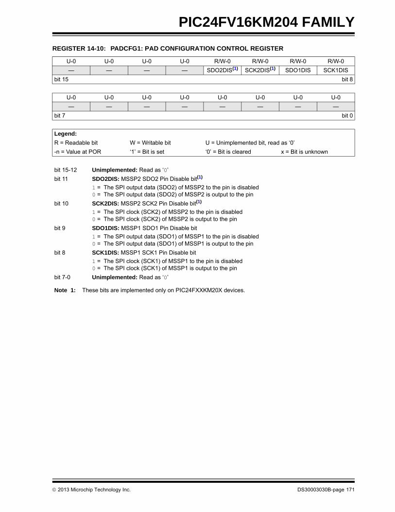
PIC24FV16KM204 FAMILY
REGISTER 14-10: PADCFG1: PAD CONFIGURATION CONTROL REGISTER
U-0 U-0 U-0 U-0 R/W-0 R/W-0 R/W-0 R/W-0
— — — — SDO2DIS(1) SCK2DIS(1) SDO1DIS SCK1DIS
bit 15 bit 8
U-0 U-0 U-0 U-0 U-0 U-0 U-0 U-0
— — — — — — — —
bit 7 bit 0
Legend:
R = Readable bit W = Writable bit U = Unimplemented bit, read as ‘0’
-n = Value at POR ‘1’ = Bit is set ‘0’ = Bit is cleared x = Bit is unknown
bit 15-12 Unimplemented: Read as ‘0’
bit 11 SDO2DIS: MSSP2 SDO2 Pin Disable bit(1)
1 = The SPI output data (SDO2) of MSSP2 to the pin is disabled0 = The SPI output data (SDO2) of MSSP2 is output to the pin
bit 10 SCK2DIS: MSSP2 SCK2 Pin Disable bit(1)
1 = The SPI clock (SCK2) of MSSP2 to the pin is disabled0 = The SPI clock (SCK2) of MSSP2 is output to the pin
bit 9 SDO1DIS: MSSP1 SDO1 Pin Disable bit
1 = The SPI output data (SDO1) of MSSP1 to the pin is disabled0 = The SPI output data (SDO1) of MSSP1 is output to the pin
bit 8 SCK1DIS: MSSP1 SCK1 Pin Disable bit
1 = The SPI clock (SCK1) of MSSP1 to the pin is disabled0 = The SPI clock (SCK1) of MSSP1 is output to the pin
bit 7-0 Unimplemented: Read as ‘0’
Note 1: These bits are implemented only on PIC24FXXKM20X devices.
2013 Microchip Technology Inc. DS30003030B-page 171

PIC24FV16KM204 FAMILY
NOTES:
DS30003030B-page 172 2013 Microchip Technology Inc.

PIC24FV16KM204 FAMILY
15.0 UNIVERSAL ASYNCHRONOUS RECEIVER TRANSMITTER (UART)
The Universal Asynchronous Receiver Transmitter(UART) module is one of the serial I/O modulesavailable in this PIC24F device family. The UART is afull-duplex, asynchronous system that can communicatewith peripheral devices, such as personal computers,LIN/J2602, RS-232 and RS-485 interfaces. This modulealso supports a hardware flow control option with theUxCTS and UxRTS pins, and also includes an IrDA®
encoder and decoder.
The primary features of the UART module are:
• Full-Duplex, 8-Bit or 9-Bit Data Transmission through the UxTX and UxRX Pins
• Even, Odd or No Parity Options (for 8-bit data)
• One or Two Stop bits
• Hardware Flow Control Option with UxCTS and UxRTS Pins
• Fully Integrated Baud Rate Generator (IBRG) with 16-Bit Prescaler
• Baud Rates Ranging from 1 Mbps to 15 bps at 16 MIPS
• 4-Deep, First-In-First-Out (FIFO) Transmit Data Buffer
• 4-Deep FIFO Receive Data Buffer
• Parity, Framing and Buffer Overrun Error Detection
• Support for 9-Bit mode with Address Detect (9th bit = 1)
• Transmit and Receive Interrupts
• Loopback mode for Diagnostic Support
• Support for Sync and Break Characters
• Supports Automatic Baud Rate Detection
• IrDA® Encoder and Decoder Logic
• 16x Baud Clock Output for IrDA Support
A simplified block diagram of the UARTx module isshown in Figure 15-1. The UARTx module consists ofthese important hardware elements:
• Baud Rate Generator
• Asynchronous Transmitter
• Asynchronous Receiver
FIGURE 15-1: UARTx MODULE SIMPLIFIED BLOCK DIAGRAM
Note: This data sheet summarizes the features ofthis group of PIC24F devices. It is notintended to be a comprehensive referencesource. For more information on the Univer-sal Asynchronous Receiver Transmitter,refer to the “PIC24F Family ReferenceManual”, “UART” (DS39708).
Note: Throughout this section, references toregister and bit names that may be asso-ciated with a specific USART module arereferred to generically by the use of ‘x’ inplace of the specific module number.Thus, “UxSTA” might refer to the USARTStatus register for either USART1 orUSART2.
UxRX
IrDA®
Hardware Flow Control
UARTx Receiver
UARTx Transmitter UxTX
UxCTS
UxRTS
UxBCLK
Baud Rate Generator
2013 Microchip Technology Inc. DS30003030B-page 173

PIC24FV16KM204 FAMILY
15.1 UARTx Baud Rate Generator (BRG)
The UARTx module includes a dedicated 16-bit BaudRate Generator (BRG). The UxBRG register controlsthe period of a free-running, 16-bit timer. Equation 15-1provides the formula for computation of the baud ratewith BRGH = 0.
EQUATION 15-1: UARTx BAUD RATE WITH BRGH = 0(1)
Example 15-1 provides the calculation of the baud rateerror for the following conditions:
• FCY = 4 MHz
• Desired Baud Rate = 9600
The maximum baud rate (BRGH = 0) possible isFCY/16 (for UxBRG = 0) and the minimum baud ratepossible is FCY/(16 * 65536).
Equation 15-2 shows the formula for computation ofthe baud rate with BRGH = 1.
EQUATION 15-2: UARTx BAUD RATE WITH BRGH = 1(1)
The maximum baud rate (BRGH = 1) possible is FCY/4(for UxBRG = 0) and the minimum baud rate possibleis FCY/(4 * 65536).
Writing a new value to the UxBRG register causes theBRG timer to be reset (cleared). This ensures the BRGdoes not wait for a timer overflow before generating thenew baud rate.
EXAMPLE 15-1: BAUD RATE ERROR CALCULATION (BRGH = 0)(1)
Note 1: Based on FCY = FOSC/2; Doze mode and PLL are disabled.
Baud Rate =FCY
16 • (UxBRG + 1)
FCY
16 • Baud RateUxBRG = – 1
Baud Rate =FCY
4 • (UxBRG + 1)
FCY
4 • Baud RateUxBRG = – 1
Note 1: Based on FCY = FOSC/2; Doze mode and PLL are disabled.
Desired Baud Rate = FCY/(16 (UxBRG + 1))
Solving for UxBRG value:
UxBRG = ((FCY/Desired Baud Rate)/16) – 1UxBRG = ((4000000/9600)/16) – 1 UxBRG = 25
Calculated Baud Rate = 4000000/(16 (25 + 1)) = 9615
Error = (Calculated Baud Rate – Desired Baud Rate)Desired Baud Rate
= (9615 – 9600)/9600 = 0.16%
Note 1: Based on FCY = FOSC/2; Doze mode and PLL are disabled.
DS30003030B-page 174 2013 Microchip Technology Inc.

PIC24FV16KM204 FAMILY
15.2 Transmitting in 8-Bit Data Mode
1. Set up the UARTx:
a) Write the appropriate values for data, parityand Stop bits.
b) Write the appropriate baud rate value to theUxBRG register.
c) Set up transmit and receive interrupt enableand priority bits.
2. Enable the UARTx.
3. Set the UTXEN bit (causes a transmit interrupt,two cycles after being set).
4. Write the data byte to the lower byte of theUxTXREG word. The value will be immediatelytransferred to the Transmit Shift Register (TSR)and the serial bit stream will start shifting outwith the next rising edge of the baud clock.
5. Alternately, the data byte may be transferredwhile UTXEN = 0, and then, the user may setUTXEN. This will cause the serial bit stream tobegin immediately, because the baud clock willstart from a cleared state.
6. A transmit interrupt will be generated as perinterrupt control bit, UTXISELx.
15.3 Transmitting in 9-Bit Data Mode
1. Set up the UARTx (as described in Section 15.2“Transmitting in 8-Bit Data Mode”).
2. Enable the UARTx.
3. Set the UTXEN bit (causes a transmit interrupt,two cycles after being set).
4. Write UxTXREG as a 16-bit value only.
5. A word write to UxTXREG triggers the transferof the 9-bit data to the TSR. The serial bit streamwill start shifting out with the first rising edge ofthe baud clock.
6. A transmit interrupt will be generated as per thesetting of control bit, UTXISELx.
15.4 Break and Sync Transmit Sequence
The following sequence will send a message frameheader, made up of a Break, followed by an Auto-BaudSync byte.
1. Configure the UARTx for the desired mode.
2. Set UTXEN and UTXBRK – this sets up theBreak character.
3. Load the UxTXREG with a dummy character toinitiate transmission (value is ignored).
4. Write ‘55h’ to UxTXREG – loads the Synccharacter into the transmit FIFO.
5. After the Break has been sent, the UTXBRK bitis reset by hardware. The Sync character nowtransmits.
15.5 Receiving in 8-Bit or 9-Bit Data Mode
1. Set up the UARTx (as described in Section 15.2“Transmitting in 8-Bit Data Mode”).
2. Enable the UARTx.
3. A receive interrupt will be generated when oneor more data characters have been received, asper interrupt control bit, URXISELx.
4. Read the OERR bit to determine if an overrunerror has occurred. The OERR bit must be resetin software.
5. Read UxRXREG.
The act of reading the UxRXREG character will movethe next character to the top of the receive FIFO,including a new set of PERR and FERR values.
15.6 Operation of UxCTS and UxRTS Control Pins
UARTx Clear-To-Send (UxCTS) and Request-To-Send(UxRTS) are the two hardware controlled pins that areassociated with the UARTx module. These two pinsallow the UARTx to operate in Simplex and Flow Con-trol modes. They are implemented to control thetransmission and reception between the Data TerminalEquipment (DTE). The UEN<1:0> bits in the UxMODEregister configure these pins.
15.7 Infrared Support
The UARTx module provides two types of infraredUARTx support: one is the IrDA clock output to supportan external IrDA encoder and decoder device (legacymodule support), and the other is the full implementationof the IrDA encoder and decoder.
As the IrDA modes require a 16x baud clock, they willonly work when the BRGH bit (UxMODE<3>) is ‘0’.
15.7.1 EXTERNAL IrDA SUPPORT – IrDA CLOCK OUTPUT
To support external IrDA encoder and decoder devices,the UxBCLK pin (same as the UxRTS pin) can beconfigured to generate the 16x baud clock. WhenUEN<1:0> = 11, the UxBCLK pin will output the 16xbaud clock if the UARTx module is enabled; it can beused to support the IrDA codec chip.
15.7.2 BUILT-IN IrDA ENCODER AND DECODER
The UARTx has full implementation of the IrDAencoder and decoder as part of the UARTx module.The built-in IrDA encoder and decoder functionality isenabled using the IREN bit (UxMODE<12>). Whenenabled (IREN = 1), the receive pin (UxRX) acts as theinput from the infrared receiver. The transmit pin(UxTX) acts as the output to the infrared transmitter.
2013 Microchip Technology Inc. DS30003030B-page 175

PIC24FV16KM204 FAMILY
REGISTER 15-1: UxMODE: UARTx MODE REGISTER
R/W-0 U-0 R/W-0 R/W-0 R/W-0 U-0 R/W-0(2) R/W-0(2)
UARTEN — USIDL IREN(1) RTSMD — UEN1 UEN0
bit 15 bit 8
R/C-0, HC R/W-0 R/W-0, HC R/W-0 R/W-0 R/W-0 R/W-0 R/W-0
WAKE LPBACK ABAUD URXINV BRGH PDSEL1 PDSEL0 STSEL
bit 7 bit 0
Legend: C = Clearable bit HC = Hardware Clearable bit
R = Readable bit W = Writable bit U = Unimplemented bit, read as ‘0’
-n = Value at POR ‘1’ = Bit is set ‘0’ = Bit is cleared x = Bit is unknown
bit 15 UARTEN: UARTx Enable bit
1 = UARTx is enabled; all UARTx pins are controlled by UARTx, as defined by UEN<1:0>0 = UARTx is disabled; all UARTx pins are controlled by port latches, UARTx power consumption is
minimal
bit 14 Unimplemented: Read as ‘0’
bit 13 USIDL: UARTx Stop in Idle Mode bit
1 = Discontinues module operation when the device enters Idle mode0 = Continues module operation in Idle mode
bit 12 IREN: IrDA® Encoder and Decoder Enable bit(1)
1 = IrDA encoder and decoder are enabled0 = IrDA encoder and decoder are disabled
bit 11 RTSMD: Mode Selection for UxRTS Pin bit
1 = UxRTS pin is in Simplex mode0 = UxRTS pin is in Flow Control mode
bit 10 Unimplemented: Read as ‘0’
bit 9-8 UEN<1:0>: UARTx Enable bits(2)
11 = UxTX, UxRX and UxBCLK pins are enabled and used; UxCTS pin is controlled by port latches10 = UxTX, UxRX, UxCTS and UxRTS pins are enabled and used01 = UxTX, UxRX and UxRTS pins are enabled and used; UxCTS pin is controlled by port latches00 = UxTX and UxRX pins are enabled and used; UxCTS and UxRTS/UxBCLK pins are controlled by port
latches
bit 7 WAKE: Wake-up on Start Bit Detect During Sleep Mode Enable bit
1 = UARTx will continue to sample the UxRX pin; interrupt is generated on the falling edge, bit iscleared in hardware on the following rising edge
0 = No wake-up is enabled
bit 6 LPBACK: UARTx Loopback Mode Select bit
1 = Enables Loopback mode0 = Loopback mode is disabled
bit 5 ABAUD: Auto-Baud Enable bit
1 = Enables baud rate measurement on the next character – requires reception of a Sync field (55h);cleared in hardware upon completion
0 = Baud rate measurement is disabled or completed
bit 4 URXINV: UARTx Receive Polarity Inversion bit
1 = UxRX Idle state is ‘0’0 = UxRX Idle state is ‘1’
Note 1: This feature is is only available for the 16x BRG mode (BRGH = 0).
2: The bit availability depends on the pin availability.
DS30003030B-page 176 2013 Microchip Technology Inc.

PIC24FV16KM204 FAMILY
bit 3 BRGH: High Baud Rate Enable bit
1 = BRG generates 4 clocks per bit period (4x baud clock, High-Speed mode)0 = BRG generates 16 clocks per bit period (16x baud clock, Standard mode)
bit 2-1 PDSEL<1:0>: Parity and Data Selection bits
11 = 9-bit data, no parity10 = 8-bit data, odd parity01 = 8-bit data, even parity00 = 8-bit data, no parity
bit 0 STSEL: Stop Bit Selection bit
1 = Two Stop bits0 = One Stop bit
REGISTER 15-1: UxMODE: UARTx MODE REGISTER (CONTINUED)
Note 1: This feature is is only available for the 16x BRG mode (BRGH = 0).
2: The bit availability depends on the pin availability.
2013 Microchip Technology Inc. DS30003030B-page 177
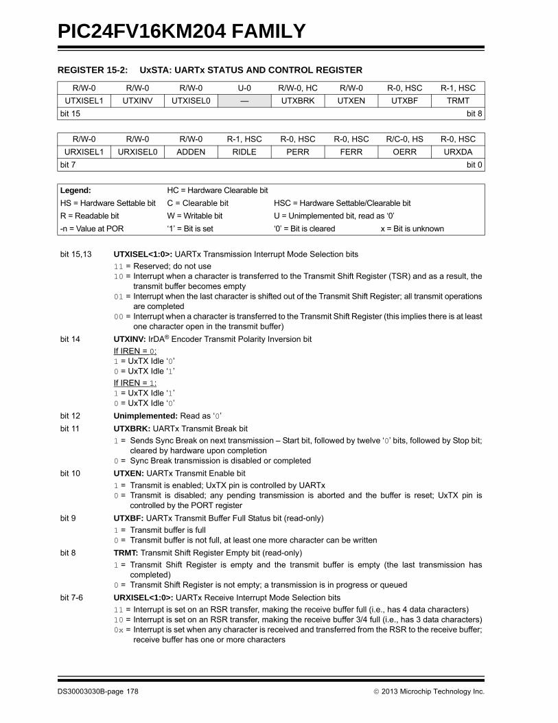
PIC24FV16KM204 FAMILY
REGISTER 15-2: UxSTA: UARTx STATUS AND CONTROL REGISTER
R/W-0 R/W-0 R/W-0 U-0 R/W-0, HC R/W-0 R-0, HSC R-1, HSC
UTXISEL1 UTXINV UTXISEL0 — UTXBRK UTXEN UTXBF TRMT
bit 15 bit 8
R/W-0 R/W-0 R/W-0 R-1, HSC R-0, HSC R-0, HSC R/C-0, HS R-0, HSC
URXISEL1 URXISEL0 ADDEN RIDLE PERR FERR OERR URXDA
bit 7 bit 0
Legend: HC = Hardware Clearable bit
HS = Hardware Settable bit C = Clearable bit HSC = Hardware Settable/Clearable bit
R = Readable bit W = Writable bit U = Unimplemented bit, read as ‘0’
-n = Value at POR ‘1’ = Bit is set ‘0’ = Bit is cleared x = Bit is unknown
bit 15,13 UTXISEL<1:0>: UARTx Transmission Interrupt Mode Selection bits
11 = Reserved; do not use10 = Interrupt when a character is transferred to the Transmit Shift Register (TSR) and as a result, the
transmit buffer becomes empty01 = Interrupt when the last character is shifted out of the Transmit Shift Register; all transmit operations
are completed00 = Interrupt when a character is transferred to the Transmit Shift Register (this implies there is at least
one character open in the transmit buffer)
bit 14 UTXINV: IrDA® Encoder Transmit Polarity Inversion bit
If IREN = 0:1 = UxTX Idle ‘0’0 = UxTX Idle ‘1’
If IREN = 1:1 = UxTX Idle ‘1’0 = UxTX Idle ‘0’
bit 12 Unimplemented: Read as ‘0’
bit 11 UTXBRK: UARTx Transmit Break bit
1 = Sends Sync Break on next transmission – Start bit, followed by twelve ‘0’ bits, followed by Stop bit;cleared by hardware upon completion
0 = Sync Break transmission is disabled or completed
bit 10 UTXEN: UARTx Transmit Enable bit
1 = Transmit is enabled; UxTX pin is controlled by UARTx0 = Transmit is disabled; any pending transmission is aborted and the buffer is reset; UxTX pin is
controlled by the PORT register
bit 9 UTXBF: UARTx Transmit Buffer Full Status bit (read-only)
1 = Transmit buffer is full0 = Transmit buffer is not full, at least one more character can be written
bit 8 TRMT: Transmit Shift Register Empty bit (read-only)
1 = Transmit Shift Register is empty and the transmit buffer is empty (the last transmission hascompleted)
0 = Transmit Shift Register is not empty; a transmission is in progress or queued
bit 7-6 URXISEL<1:0>: UARTx Receive Interrupt Mode Selection bits
11 = Interrupt is set on an RSR transfer, making the receive buffer full (i.e., has 4 data characters)10 = Interrupt is set on an RSR transfer, making the receive buffer 3/4 full (i.e., has 3 data characters)0x = Interrupt is set when any character is received and transferred from the RSR to the receive buffer;
receive buffer has one or more characters
DS30003030B-page 178 2013 Microchip Technology Inc.

PIC24FV16KM204 FAMILY
bit 5 ADDEN: Address Character Detect bit (bit 8 of received data = 1)
1 = Address Detect mode is enabled; if 9-bit mode is not selected, this does not take effect0 = Address Detect mode is disabled
bit 4 RIDLE: Receiver Idle bit (read-only)
1 = Receiver is Idle0 = Receiver is active
bit 3 PERR: Parity Error Status bit (read-only)
1 = Parity error has been detected for the current character (character at the top of the receive FIFO)0 = Parity error has not been detected
bit 2 FERR: Framing Error Status bit (read-only)
1 = Framing error has been detected for the current character (character at the top of the receive FIFO)0 = Framing error has not been detected
bit 1 OERR: Receive Buffer Overrun Error Status bit (clear/read-only)
1 = Receive buffer has overflowed0 = Receive buffer has not overflowed (clearing a previously set OERR bit (1 0 transition) will reset
the receiver buffer and the RSR to the empty state)
bit 0 URXDA: UARTx Receive Buffer Data Available bit (read-only)
1 = Receive buffer has data; at least one more characters can be read0 = Receive buffer is empty
REGISTER 15-2: UxSTA: UARTx STATUS AND CONTROL REGISTER (CONTINUED)
2013 Microchip Technology Inc. DS30003030B-page 179

PIC24FV16KM204 FAMILY
REGISTER 15-3: UxTXREG: UARTx TRANSMIT REGISTER
U-x U-x U-x U-x U-x U-x U-x W-x
— — — — — — — UTX8
bit 15 bit 8
W-x W-x W-x W-x W-x W-x W-x W-x
UTX7 UTX6 UTX5 UTX4 UTX3 UTX2 UTX1 UTX0
bit 7 bit 0
Legend:
R = Readable bit W = Writable bit U = Unimplemented bit, read as ‘0’
-n = Value at POR ‘1’ = Bit is set ‘0’ = Bit is cleared x = Bit is unknown
bit 15-9 Unimplemented: Read as ‘0’
bit 8 UTX8: Data of the Transmitted Character bit (in 9-bit mode)
bit 7-0 UTX<7:0>: Data of the Transmitted Character bits
REGISTER 15-4: UxRXREG: UARTx RECEIVE REGISTER
U-0 U-0 U-0 U-0 U-0 U-0 U-0 R-0, HSC
— — — — — — — URX8
bit 15 bit 8
R-0, HSC R-0, HSC R-0, HSC R-0, HSC R-0, HSC R-0, HSC R-0, HSC R-0, HSC
URX7 URX6 URX5 URX4 URX3 URX2 URX1 URX0
bit 7 bit 0
Legend: HSC = Hardware Settable/Clearable bit
R = Readable bit W = Writable bit U = Unimplemented bit, read as ‘0’
-n = Value at POR ‘1’ = Bit is set ‘0’ = Bit is cleared x = Bit is unknown
bit 15-9 Unimplemented: Read as ‘0’
bit 8 URX8: Data of the Received Character bit (in 9-bit mode)
bit 7-0 URX<7:0>: Data of the Received Character bits
DS30003030B-page 180 2013 Microchip Technology Inc.

PIC24FV16KM204 FAMILY
16.0 REAL-TIME CLOCK AND CALENDAR (RTCC)
The RTCC provides the user with a Real-Time Clockand Calendar (RTCC) function that can be calibrated.
Key features of the RTCC module are:
• Operates in Sleep and Retention Sleep modes
• Selectable clock source
• Provides hours, minutes and seconds using 24-hour format
• Visibility of one half second period
• Provides calendar – weekday, date, month and year
• Alarm-configurable for half a second, one second, 10 seconds, one minute, 10 minutes, one hour, one day, one week, one month or one year
• Alarm repeat with decrementing counter
• Alarm with indefinite repeat chime
• Year 2000 to 2099 leap year correction
• BCD format for smaller software overhead
• Optimized for long term battery operation
• User calibration of the 32.768 kHz clock crystal/32K INTRC frequency with periodic auto-adjust
• Optimized for long term battery operation
• Fractional second synchronization
• Calibration to within ±2.64 seconds error per month
• Calibrates up to 260 ppm of crystal error
• Ability to periodically wake-up external devices without CPU intervention (external power control)
• Power control output for external circuit control
• Calibration takes effect every 15 seconds
• Runs from any one of the following:
- External Real-Time Clock of 32.768 kHz- Internal 31.25 kHz LPRC Clock- 50 Hz or 60 Hz External Input
16.1 RTCC Source Clock
The user can select between the SOSC crystaloscillator, LPRC internal oscillator or an external50 Hz/60 Hz power line input as the clock reference forthe RTCC module. This gives the user an option to tradeoff system cost, accuracy and power consumption,based on the overall system needs.
FIGURE 16-1: RTCC BLOCK DIAGRAM
Note: This data sheet summarizes the features ofthis group of PIC24F devices. It is notintended to be a comprehensive referencesource. For more information on theReal-Time Clock and Calendar, refer to the“PIC24F Family Reference Manual”,“Real-Time Clock and Calendar(RTCC)” (DS39696).
RTCC Clock Domain CPU Clock Domain
RTCC
RTCC Prescalers
RTCC Timer
Comparator
Alarm Registers with Masks
Repeat Counter
0.5 Sec
RTCC Interrupt Logic
ALRMVAL
ALCFGRPT
RCFGCAL
Alarm Event
YEARMTHDY
WKDYHRMINSEC
ALMTHDYALWDHR
ALMINSEC
RTCC Interrupt
RTCOUT<1:0>
RTCOE
Clock Source
1s
Pin
Alarm Pulse
Input fromSOSC/LPRCOscillator orExternal Source
RTCVAL
2013 Microchip Technology Inc. DS30003030B-page 181

PIC24FV16KM204 FAMILY
16.2 RTCC Module Registers
The RTCC module registers are organized into threecategories:
• RTCC Control Registers
• RTCC Value Registers
• Alarm Value Registers
16.2.1 REGISTER MAPPING
To limit the register interface, the RTCC Timer andAlarm Time registers are accessed through corre-sponding register pointers. The RTCC Value registerwindow (RTCVALH and RTCVALL) uses the RTCPTRxbits (RCFGCAL<9:8>) to select the desired Timerregister pair (see Table 16-1).
By writing the RTCVALH byte, the RTCC Pointer value,the RTCPTR<1:0> bits decrement by one until they reach‘00’. Once they reach ‘00’, the MINUTES and SECONDSvalue will be accessible through RTCVALH andRTCVALL until the pointer value is manually changed.
TABLE 16-1: RTCVAL REGISTER MAPPING
The Alarm Value register window (ALRMVALH andALRMVALL) uses the ALRMPTRx bits(ALCFGRPT<9:8>) to select the desired Alarmregister pair (see Table 16-2).
By writing the ALRMVALH byte, the ALRMPTR<1:0>bits (Alarm Pointer value) decrement by one until theyreach ‘00’. Once they reach ‘00’, the ALRMMIN andALRMSEC value will be accessible throughALRMVALH and ALRMVALL, until the pointer value ismanually changed.
TABLE 16-2: ALRMVAL REGISTER MAPPING
Considering that the 16-bit core does not distinguishbetween 8-bit and 16-bit read operations, the user mustbe aware that when reading either the ALRMVALH orALRMVALL bytes, the ALRMPTR<1:0> value will bedecremented. The same applies to the RTCVALH orRTCVALL bytes with the RTCPTR<1:0> beingdecremented.
16.2.2 WRITE LOCK
In order to perform a write to any of the RTCC Timerregisters, the RTCWREN bit (RCFGCAL<13>) must beset (see Example 16-1 and Example 16-2).
16.2.3 SELECTING RTCC CLOCK SOURCE
There are four reference source clock options that canbe selected for the RTCC using the RTCCLK<1:0>bits (RTCPWC<11:10>): 00 = Secondary Oscillator,01 = LPRC, 10 = 50 Hz External Clock and 11 = 60 HzExternal Clock.
EXAMPLE 16-1: SETTING THE RTCWREN BIT IN ASSEMBLY
EXAMPLE 16-2: SETTING THE RTCWREN BIT IN ‘C’
RTCPTR<1:0>RTCC Value Register Window
RTCVAL<15:8> RTCVAL<7:0>
00 MINUTES SECONDS
01 WEEKDAY HOURS
10 MONTH DAY
11 — YEAR
ALRMPTR<1:0>
Alarm Value Register Window
ALRMVALH<15:8> ALRMVALL<7:0>
00 ALRMMIN ALRMSEC
01 ALRMWD ALRMHR
10 ALRMMNTH ALRMDAY
11 PWCSTAB PWCSAMP
Note: This only applies to read operations andnot write operations.
Note: To avoid accidental writes to the timer, it isrecommended that the RTCWREN bit(RCFGCAL<13>) is kept clear at anyother time. For the RTCWREN bit to beset, there is only one instruction cycle timewindow allowed between the 55h/AAsequence and the setting of RTCWREN.Therefore, it is recommended that codefollow the procedure in Example 16-2.
push w7 ; Store W7 and W8 values on the stack.push w8disi #5 ; Disable interrupts until sequence is complete.mov #0x55, w7 ; Write 0x55 unlock value to NVMKEY.mov w7, NVMKEYmov #0xAA, w8 ; Write 0xAA unlock value to NVMKEY.mov w8, NVMKEYbset RCFGCAL, #13 ; Set the RTCWREN bit.pop w8 ; Restore the original W register values from the stack.pop w7
//This builtin function executes implements the unlock sequence and sets//the RTCWREN bit.__builtin_write_RTCWEN();
DS30003030B-page 182 2013 Microchip Technology Inc.
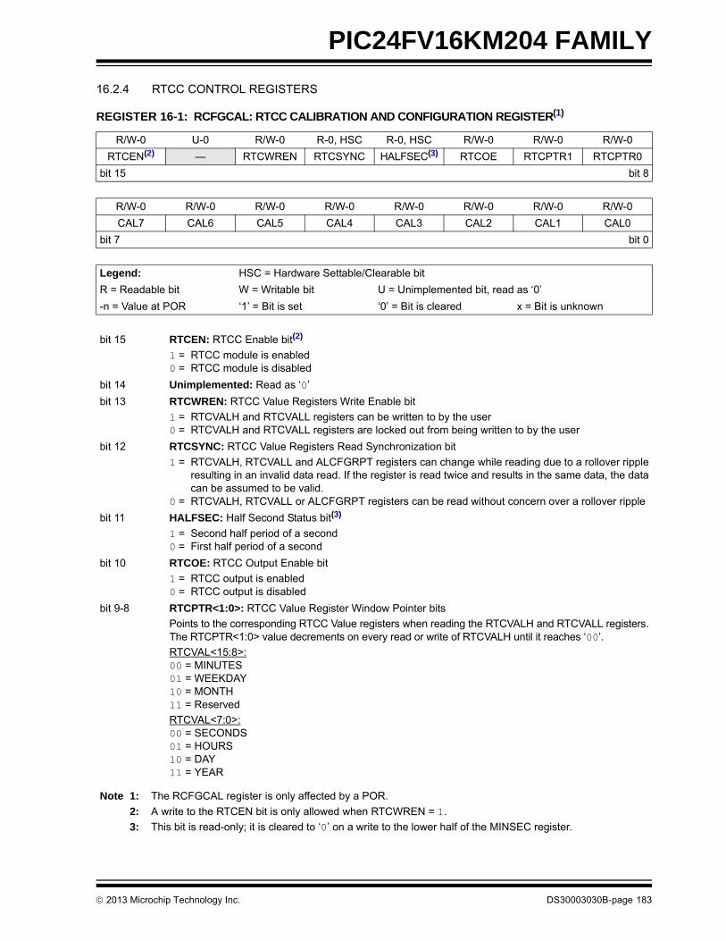
PIC24FV16KM204 FAMILY
16.2.4 RTCC CONTROL REGISTERS
REGISTER 16-1: RCFGCAL: RTCC CALIBRATION AND CONFIGURATION REGISTER(1)
R/W-0 U-0 R/W-0 R-0, HSC R-0, HSC R/W-0 R/W-0 R/W-0
RTCEN(2) — RTCWREN RTCSYNC HALFSEC(3) RTCOE RTCPTR1 RTCPTR0
bit 15 bit 8
R/W-0 R/W-0 R/W-0 R/W-0 R/W-0 R/W-0 R/W-0 R/W-0
CAL7 CAL6 CAL5 CAL4 CAL3 CAL2 CAL1 CAL0
bit 7 bit 0
Legend: HSC = Hardware Settable/Clearable bit
R = Readable bit W = Writable bit U = Unimplemented bit, read as ‘0’
-n = Value at POR ‘1’ = Bit is set ‘0’ = Bit is cleared x = Bit is unknown
bit 15 RTCEN: RTCC Enable bit(2)
1 = RTCC module is enabled0 = RTCC module is disabled
bit 14 Unimplemented: Read as ‘0’
bit 13 RTCWREN: RTCC Value Registers Write Enable bit
1 = RTCVALH and RTCVALL registers can be written to by the user0 = RTCVALH and RTCVALL registers are locked out from being written to by the user
bit 12 RTCSYNC: RTCC Value Registers Read Synchronization bit
1 = RTCVALH, RTCVALL and ALCFGRPT registers can change while reading due to a rollover rippleresulting in an invalid data read. If the register is read twice and results in the same data, the datacan be assumed to be valid.
0 = RTCVALH, RTCVALL or ALCFGRPT registers can be read without concern over a rollover ripple
bit 11 HALFSEC: Half Second Status bit(3)
1 = Second half period of a second0 = First half period of a second
bit 10 RTCOE: RTCC Output Enable bit
1 = RTCC output is enabled0 = RTCC output is disabled
bit 9-8 RTCPTR<1:0>: RTCC Value Register Window Pointer bits
Points to the corresponding RTCC Value registers when reading the RTCVALH and RTCVALL registers.The RTCPTR<1:0> value decrements on every read or write of RTCVALH until it reaches ‘00’.
RTCVAL<15:8>:00 = MINUTES01 = WEEKDAY10 = MONTH11 = Reserved
RTCVAL<7:0>:00 = SECONDS01 = HOURS10 = DAY11 = YEAR
Note 1: The RCFGCAL register is only affected by a POR.
2: A write to the RTCEN bit is only allowed when RTCWREN = 1.
3: This bit is read-only; it is cleared to ‘0’ on a write to the lower half of the MINSEC register.
2013 Microchip Technology Inc. DS30003030B-page 183
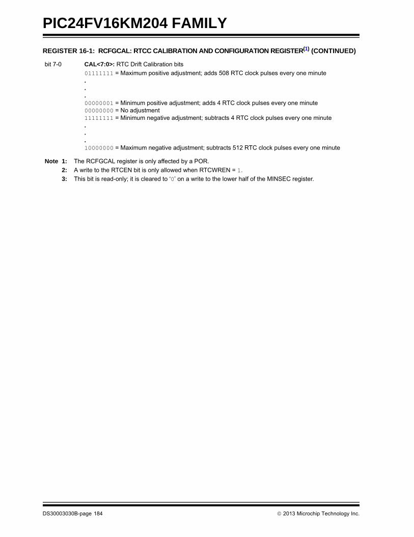
PIC24FV16KM204 FAMILY
bit 7-0 CAL<7:0>: RTC Drift Calibration bits
01111111 = Maximum positive adjustment; adds 508 RTC clock pulses every one minute...00000001 = Minimum positive adjustment; adds 4 RTC clock pulses every one minute00000000 = No adjustment11111111 = Minimum negative adjustment; subtracts 4 RTC clock pulses every one minute...10000000 = Maximum negative adjustment; subtracts 512 RTC clock pulses every one minute
REGISTER 16-1: RCFGCAL: RTCC CALIBRATION AND CONFIGURATION REGISTER(1) (CONTINUED)
Note 1: The RCFGCAL register is only affected by a POR.
2: A write to the RTCEN bit is only allowed when RTCWREN = 1.
3: This bit is read-only; it is cleared to ‘0’ on a write to the lower half of the MINSEC register.
DS30003030B-page 184 2013 Microchip Technology Inc.

PIC24FV16KM204 FAMILY
REGISTER 16-2: RTCPWC: RTCC CONFIGURATION REGISTER 2(1)
R/W-0 R/W-0 R/W-0 R/W-0 R/W-0 R/W-0 R/W-0 R/W-0
PWCEN PWCPOL PWCCPRE PWCSPRE RTCCLK1(2) RTCCLK0(2) RTCOUT1 RTCOUT0
bit 15 bit 8
U-0 U-0 U-0 U-0 U-0 U-0 U-0 U-0
— — — — — — — —
bit 7 bit 0
Legend:
R = Readable bit W = Writable bit U = Unimplemented bit, read as ‘0’
-n = Value at POR ‘1’ = Bit is set ‘0’ = Bit is cleared x = Bit is unknown
bit 15 PWCEN: Power Control Enable bit
1 = Power control is enabled0 = Power control is disabled
bit 14 PWCPOL: Power Control Polarity bit
1 = Power control output is active-high0 = Power control output is active-low
bit 13 PWCCPRE: Power Control/Stability Prescaler bits
1 = PWC stability window clock is divide-by-2 of source RTCC clock0 = PWC stability window clock is divide-by-1 of source RTCC clock
bit 12 PWCSPRE: Power Control Sample Prescaler bits
1 = PWC sample window clock is divide-by-2 of source RTCC clock0 = PWC sample window clock is divide-by-1 of source RTCC clock
bit 11-10 RTCCLK<1:0>: RTCC Clock Select bits(2)
Determines the source of the internal RTCC clock, which is used for all RTCC timer operations.00 = External Secondary Oscillator (SOSC) 01 = Internal LPRC Oscillator10 = External power line source – 50 Hz 11 = External power line source – 60 Hz
bit 9-8 RTCOUT<1:0>: RTCC Output Select bits
Determines the source of the RTCC pin output.00 = RTCC alarm pulse 01 = RTCC seconds clock 10 = RTCC clock 11 = Power control
bit 7-0 Unimplemented: Read as ‘0’
Note 1: The RTCPWC register is only affected by a POR.
2: When a new value is written to these register bits, the Seconds Value register should also be written to properly reset the clock prescalers in the RTCC.
2013 Microchip Technology Inc. DS30003030B-page 185
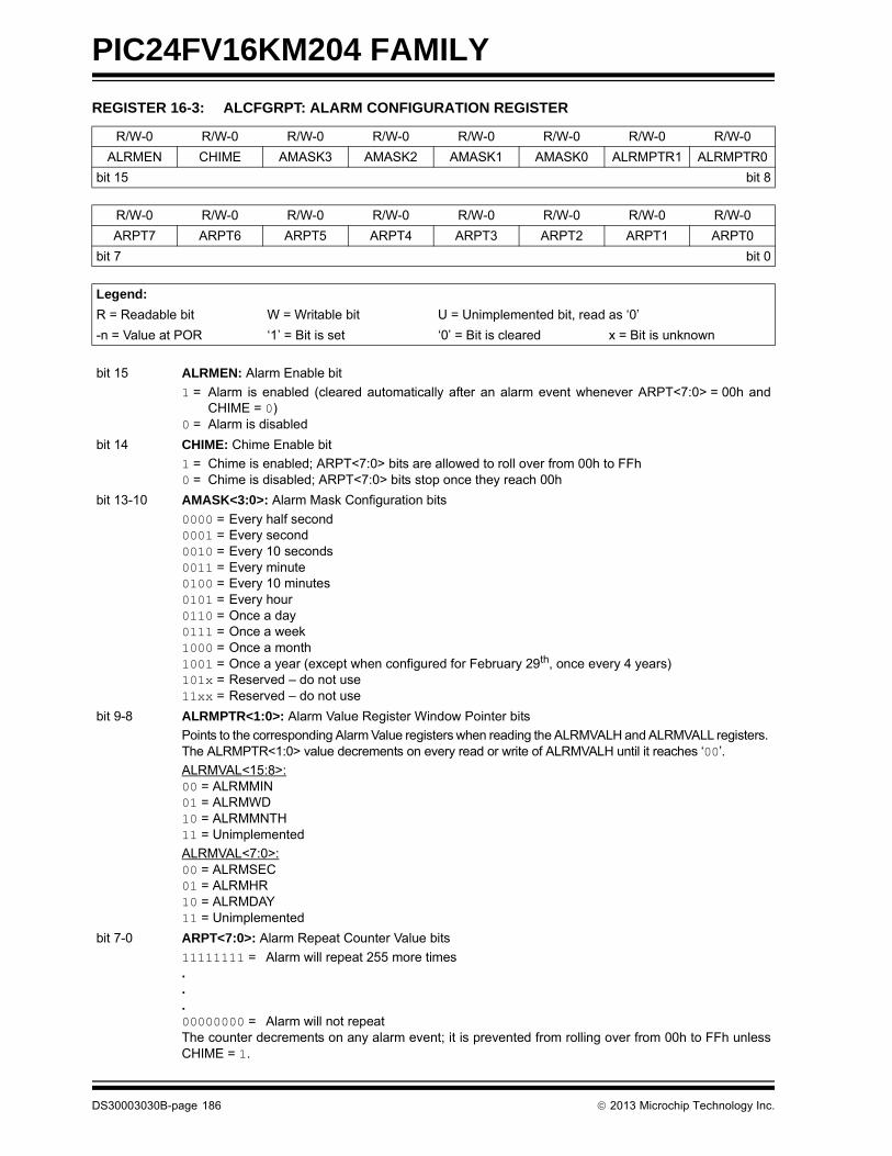
PIC24FV16KM204 FAMILY
REGISTER 16-3: ALCFGRPT: ALARM CONFIGURATION REGISTER
R/W-0 R/W-0 R/W-0 R/W-0 R/W-0 R/W-0 R/W-0 R/W-0
ALRMEN CHIME AMASK3 AMASK2 AMASK1 AMASK0 ALRMPTR1 ALRMPTR0
bit 15 bit 8
R/W-0 R/W-0 R/W-0 R/W-0 R/W-0 R/W-0 R/W-0 R/W-0
ARPT7 ARPT6 ARPT5 ARPT4 ARPT3 ARPT2 ARPT1 ARPT0
bit 7 bit 0
Legend:
R = Readable bit W = Writable bit U = Unimplemented bit, read as ‘0’
-n = Value at POR ‘1’ = Bit is set ‘0’ = Bit is cleared x = Bit is unknown
bit 15 ALRMEN: Alarm Enable bit
1 = Alarm is enabled (cleared automatically after an alarm event whenever ARPT<7:0> = 00h andCHIME = 0)
0 = Alarm is disabled
bit 14 CHIME: Chime Enable bit
1 = Chime is enabled; ARPT<7:0> bits are allowed to roll over from 00h to FFh0 = Chime is disabled; ARPT<7:0> bits stop once they reach 00h
bit 13-10 AMASK<3:0>: Alarm Mask Configuration bits
0000 = Every half second0001 = Every second0010 = Every 10 seconds0011 = Every minute0100 = Every 10 minutes0101 = Every hour0110 = Once a day0111 = Once a week1000 = Once a month1001 = Once a year (except when configured for February 29th, once every 4 years)101x = Reserved – do not use11xx = Reserved – do not use
bit 9-8 ALRMPTR<1:0>: Alarm Value Register Window Pointer bits
Points to the corresponding Alarm Value registers when reading the ALRMVALH and ALRMVALL registers. The ALRMPTR<1:0> value decrements on every read or write of ALRMVALH until it reaches ‘00’.
ALRMVAL<15:8>:00 = ALRMMIN01 = ALRMWD10 = ALRMMNTH11 = Unimplemented
ALRMVAL<7:0>:00 = ALRMSEC01 = ALRMHR10 = ALRMDAY11 = Unimplemented
bit 7-0 ARPT<7:0>: Alarm Repeat Counter Value bits
11111111 = Alarm will repeat 255 more times...00000000 = Alarm will not repeatThe counter decrements on any alarm event; it is prevented from rolling over from 00h to FFh unlessCHIME = 1.
DS30003030B-page 186 2013 Microchip Technology Inc.

PIC24FV16KM204 FAMILY
16.2.5 RTCVAL REGISTER MAPPINGS
REGISTER 16-4: YEAR: YEAR VALUE REGISTER(1)
U-0 U-0 U-0 U-0 U-0 U-0 U-0 U-0
— — — — — — — —
bit 15 bit 8
R/W-x R/W-x R/W-x R/W-x R/W-x R/W-x R/W-x R/W-x
YRTEN3 YRTEN2 YRTEN1 YRTEN0 YRONE3 YRONE2 YRONE1 YRONE0
bit 7 bit 0
Legend:
R = Readable bit W = Writable bit U = Unimplemented bit, read as ‘0’
-n = Value at POR ‘1’ = Bit is set ‘0’ = Bit is cleared x = Bit is unknown
bit 15-8 Unimplemented: Read as ‘0’
bit 7-4 YRTEN<3:0>: Binary Coded Decimal Value of Year’s Tens Digit bits
Contains a value from 0 to 9.
bit 3-0 YRONE<3:0>: Binary Coded Decimal Value of Year’s Ones Digit bits
Contains a value from 0 to 9.
Note 1: A write to the YEAR register is only allowed when RTCWREN = 1.
REGISTER 16-5: MTHDY: MONTH AND DAY VALUE REGISTER(1)
U-0 U-0 U-0 R/W-x R/W-x R/W-x R/W-x R/W-x
— — — MTHTEN0 MTHONE3 MTHONE2 MTHONE1 MTHONE0
bit 15 bit 8
U-0 U-0 R/W-x R/W-x R/W-x R/W-x R/W-x R/W-x
— — DAYTEN1 DAYTEN0 DAYONE3 DAYONE2 DAYONE1 DAYONE0
bit 7 bit 0
Legend:
R = Readable bit W = Writable bit U = Unimplemented bit, read as ‘0’
-n = Value at POR ‘1’ = Bit is set ‘0’ = Bit is cleared x = Bit is unknown
bit 15-13 Unimplemented: Read as ‘0’
bit 12 MTHTEN0: Binary Coded Decimal Value of Month’s Tens Digit bitContains a value of ‘0’ or ‘1’.
bit 11-8 MTHONE<3:0>: Binary Coded Decimal Value of Month’s Ones Digit bits
Contains a value from 0 to 9.
bit 7-6 Unimplemented: Read as ‘0’
bit 5-4 DAYTEN<1:0>: Binary Coded Decimal Value of Day’s Tens Digit bits
Contains a value from 0 to 3.
bit 3-0 DAYONE<3:0>: Binary Coded Decimal Value of Day’s Ones Digit bits
Contains a value from 0 to 9.
Note 1: A write to this register is only allowed when RTCWREN = 1.
2013 Microchip Technology Inc. DS30003030B-page 187

PIC24FV16KM204 FAMILY
REGISTER 16-6: WKDYHR: WEEKDAY AND HOURS VALUE REGISTER(1)
U-0 U-0 U-0 U-0 U-0 R/W-x R/W-x R/W-x
— — — — — WDAY2 WDAY1 WDAY0
bit 15 bit 8
U-0 U-0 R/W-x R/W-x R/W-x R/W-x R/W-x R/W-x
— — HRTEN1 HRTEN0 HRONE3 HRONE2 HRONE1 HRONE0
bit 7 bit 0
Legend:
R = Readable bit W = Writable bit U = Unimplemented bit, read as ‘0’
-n = Value at POR ‘1’ = Bit is set ‘0’ = Bit is cleared x = Bit is unknown
bit 15-11 Unimplemented: Read as ‘0’
bit 10-8 WDAY<2:0>: Binary Coded Decimal Value of Weekday Digit bits
Contains a value from 0 to 6.
bit 7-6 Unimplemented: Read as ‘0’
bit 5-4 HRTEN<1:0>: Binary Coded Decimal Value of Hour’s Tens Digit bits
Contains a value from 0 to 2.
bit 3-0 HRONE<3:0>: Binary Coded Decimal Value of Hour’s Ones Digit bits
Contains a value from 0 to 9.
Note 1: A write to this register is only allowed when RTCWREN = 1.
REGISTER 16-7: MINSEC: MINUTES AND SECONDS VALUE REGISTER
U-0 R/W-x R/W-x R/W-x R/W-x R/W-x R/W-x R/W-x
— MINTEN2 MINTEN1 MINTEN0 MINONE3 MINONE2 MINONE1 MINONE0
bit 15 bit 8
U-0 R/W-x R/W-x R/W-x R/W-x R/W-x R/W-x R/W-x
— SECTEN2 SECTEN1 SECTEN0 SECONE3 SECONE2 SECONE1 SECONE0
bit 7 bit 0
Legend:
R = Readable bit W = Writable bit U = Unimplemented bit, read as ‘0’
-n = Value at POR ‘1’ = Bit is set ‘0’ = Bit is cleared x = Bit is unknown
bit 15 Unimplemented: Read as ‘0’
bit 14-12 MINTEN<2:0>: Binary Coded Decimal Value of Minute’s Tens Digit bits
Contains a value from 0 to 5.
bit 11-8 MINONE<3:0>: Binary Coded Decimal Value of Minute’s Ones Digit bits
Contains a value from 0 to 9.
bit 7 Unimplemented: Read as ‘0’
bit 6-4 SECTEN<2:0>: Binary Coded Decimal Value of Second’s Tens Digit bits
Contains a value from 0 to 5.
bit 3-0 SECONE<3:0>: Binary Coded Decimal Value of Second’s Ones Digit bits
Contains a value from 0 to 9.
DS30003030B-page 188 2013 Microchip Technology Inc.

PIC24FV16KM204 FAMILY
16.2.6 ALRMVAL REGISTER MAPPINGS
REGISTER 16-8: ALMTHDY: ALARM MONTH AND DAY VALUE REGISTER(1)
U-0 U-0 U-0 R/W-x R/W-x R/W-x R/W-x R/W-x
— — — MTHTEN0 MTHONE3 MTHONE2 MTHONE1 MTHONE0
bit 15 bit 8
U-0 U-0 R/W-x R/W-x R/W-x R/W-x R/W-x R/W-x
— — DAYTEN1 DAYTEN0 DAYONE3 DAYONE2 DAYONE1 DAYONE0
bit 7 bit 0
Legend:
R = Readable bit W = Writable bit U = Unimplemented bit, read as ‘0’
-n = Value at POR ‘1’ = Bit is set ‘0’ = Bit is cleared x = Bit is unknown
bit 15-13 Unimplemented: Read as ‘0’
bit 12 MTHTEN0: Binary Coded Decimal Value of Month’s Tens Digit bitContains a value of ‘0’ or ‘1’.
bit 11-8 MTHONE<3:0>: Binary Coded Decimal Value of Month’s Ones Digit bitsContains a value from 0 to 9.
bit 7-6 Unimplemented: Read as ‘0’
bit 5-4 DAYTEN<1:0>: Binary Coded Decimal Value of Day’s Tens Digit bitsContains a value from 0 to 3.
bit 3-0 DAYONE<3:0>: Binary Coded Decimal Value of Day’s Ones Digit bitsContains a value from 0 to 9.
Note 1: A write to this register is only allowed when RTCWREN = 1.
REGISTER 16-9: ALWDHR: ALARM WEEKDAY AND HOURS VALUE REGISTER(1)
U-0 U-0 U-0 U-0 U-0 R/W-x R/W-x R/W-x
— — — — — WDAY2 WDAY1 WDAY0
bit 15 bit 8
U-0 U-0 R/W-x R/W-x R/W-x R/W-x R/W-x R/W-x
— — HRTEN1 HRTEN0 HRONE3 HRONE2 HRONE1 HRONE0
bit 7 bit 0
Legend:
R = Readable bit W = Writable bit U = Unimplemented bit, read as ‘0’
-n = Value at POR ‘1’ = Bit is set ‘0’ = Bit is cleared x = Bit is unknown
bit 15-11 Unimplemented: Read as ‘0’
bit 10-8 WDAY<2:0>: Binary Coded Decimal Value of Weekday Digit bitsContains a value from 0 to 6.
bit 7-6 Unimplemented: Read as ‘0’
bit 5-4 HRTEN<1:0>: Binary Coded Decimal Value of Hour’s Tens Digit bitsContains a value from 0 to 2.
bit 3-0 HRONE<3:0>: Binary Coded Decimal Value of Hour’s Ones Digit bitsContains a value from 0 to 9.
Note 1: A write to this register is only allowed when RTCWREN = 1.
2013 Microchip Technology Inc. DS30003030B-page 189

PIC24FV16KM204 FAMILY
REGISTER 16-10: ALMINSEC: ALARM MINUTES AND SECONDS VALUE REGISTER
U-0 R/W-x R/W-x R/W-x R/W-x R/W-x R/W-x R/W-x
— MINTEN2 MINTEN1 MINTEN0 MINONE3 MINONE2 MINONE1 MINONE0
bit 15 bit 8
U-0 R/W-x R/W-x R/W-x R/W-x R/W-x R/W-x R/W-x
— SECTEN2 SECTEN1 SECTEN0 SECONE3 SECONE2 SECONE1 SECONE0
bit 7 bit 0
Legend:
R = Readable bit W = Writable bit U = Unimplemented bit, read as ‘0’
-n = Value at POR ‘1’ = Bit is set ‘0’ = Bit is cleared x = Bit is unknown
bit 15 Unimplemented: Read as ‘0’
bit 14-12 MINTEN<2:0>: Binary Coded Decimal Value of Minute’s Tens Digit bits
Contains a value from 0 to 5.
bit 11-8 MINONE<3:0>: Binary Coded Decimal Value of Minute’s Ones Digit bits
Contains a value from 0 to 9.
bit 7 Unimplemented: Read as ‘0’
bit 6-4 SECTEN<2:0>: Binary Coded Decimal Value of Second’s Tens Digit bits
Contains a value from 0 to 5.
bit 3-0 SECONE<3:0>: Binary Coded Decimal Value of Second’s Ones Digit bits
Contains a value from 0 to 9.
DS30003030B-page 190 2013 Microchip Technology Inc.

PIC24FV16KM204 FAMILY
REGISTER 16-11: RTCCSWT: RTCC CONTROL/SAMPLE WINDOW TIMER REGISTER(1)
R/W-x R/W-x R/W-x R/W-x R/W-x R/W-x R/W-x R/W-x
PWCSTAB7 PWCSTAB6 PWCSTAB5 PWCSTAB4 PWCSTAB3 PWCSTAB2 PWCSTAB1 PWCSTAB0
bit 15 bit 8
R/W-x R/W-x R/W-x R/W-x R/W-x R/W-x R/W-x R/W-x
PWCSAMP7 PWCSAMP6 PWCSAMP5 PWCSAMP4 PWCSAMP3 PWCSAMP2 PWCSAMP1 PWCSAMP0
bit 7 bit 0
Legend:
R = Readable bit W = Writable bit U = Unimplemented bit, read as ‘0’
-n = Value at POR ‘1’ = Bit is set ‘0’ = Bit is cleared x = Bit is unknown
bit 15-8 PWCSTAB<7:0>: PWM Stability Window Timer bits
11111111 = Stability window is 255 TPWCCLK clock periods...00000000 = Stability window is 0 TPWCCLK clock periods The sample window starts when the alarm event triggers. The stability window timer starts countingfrom every alarm event when PWCEN = 1.
bit 7-0 PWCSAMP<7:0>: PWM Sample Window Timer bits
11111111 = Sample window is always enabled, even when PWCEN = 011111110 = Sample window is 254 TPWCCLK clock periods...00000000 = Sample window is 0 TPWCCLK clock periodsThe sample window timer starts counting at the end of the stability window when PWCEN = 1. IfPWCSTAB<7:0> = 00000000, the sample window timer starts counting from every alarm event whenPWCEN = 1.
Note 1: A write to this register is only allowed when RTCWREN = 1.
2013 Microchip Technology Inc. DS30003030B-page 191
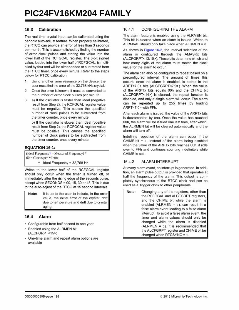
PIC24FV16KM204 FAMILY
16.3 Calibration
The real-time crystal input can be calibrated using theperiodic auto-adjust feature. When properly calibrated,the RTCC can provide an error of less than 3 secondsper month. This is accomplished by finding the numberof error clock pulses and storing the value into thelower half of the RCFGCAL register. The 8-bit signedvalue, loaded into the lower half of RCFGCAL, is multi-plied by four and will be either added or subtracted fromthe RTCC timer, once every minute. Refer to the stepsbelow for RTCC calibration:
1. Using another timer resource on the device, theuser must find the error of the 32.768 kHz crystal.
2. Once the error is known, it must be converted tothe number of error clock pulses per minute.
3. a) If the oscillator is faster than ideal (negativeresult from Step 2), the RCFGCAL register valuemust be negative. This causes the specifiednumber of clock pulses to be subtracted fromthe timer counter, once every minute.
b) If the oscillator is slower than ideal (positiveresult from Step 2), the RCFGCAL register valuemust be positive. This causes the specifiednumber of clock pulses to be subtracted fromthe timer counter, once every minute.
EQUATION 16-1:
Writes to the lower half of the RCFGCAL registershould only occur when the timer is turned off, orimmediately after the rising edge of the seconds pulse,except when SECONDS = 00, 15, 30 or 45. This is dueto the auto-adjust of the RTCC at 15 second intervals.
16.4 Alarm
• Configurable from half second to one year
• Enabled using the ALRMEN bit (ALCFGRPT<15>)
• One-time alarm and repeat alarm options are available
16.4.1 CONFIGURING THE ALARM
The alarm feature is enabled using the ALRMEN bit.This bit is cleared when an alarm is issued. Writes toALRMVAL should only take place when ALRMEN = 0.
As shown in Figure 16-2, the interval selection of thealarm is configured through the AMASKx bits(ALCFGRPT<13:10>). These bits determine which andhow many digits of the alarm must match the clockvalue for the alarm to occur.
The alarm can also be configured to repeat based on apreconfigured interval. The amount of times thisoccurs, once the alarm is enabled, is stored in theARPT<7:0> bits (ALCFGRPT<7:0>). When the valueof the ARPTx bits equals 00h and the CHIME bit(ALCFGRPT<14>) is cleared, the repeat function isdisabled, and only a single alarm will occur. The alarmcan be repeated up to 255 times by loadingARPT<7:0> with FFh.
After each alarm is issued, the value of the ARPTx bitsis decremented by one. Once the value has reached00h, the alarm will be issued one last time, after which,the ALRMEN bit will be cleared automatically and thealarm will turn off.
Indefinite repetition of the alarm can occur if theCHIME bit = 1. Instead of the alarm being disabledwhen the value of the ARPTx bits reaches 00h, it rollsover to FFh and continues counting indefinitely whileCHIME is set.
16.4.2 ALARM INTERRUPT
At every alarm event, an interrupt is generated. In addi-tion, an alarm pulse output is provided that operates athalf the frequency of the alarm. This output is com-pletely synchronous to the RTCC clock and can beused as a Trigger clock to other peripherals.
(Ideal Frequency† – Measured Frequency) * 60 = Clocks per Minute
† Ideal Frequency = 32,768 Hz
Note: It is up to the user to include, in the errorvalue, the initial error of the crystal: driftdue to temperature and drift due to crystalaging.
Note: Changing any of the registers, other thanthe RCFGCAL and ALCFGRPT registers,and the CHIME bit while the alarm isenabled (ALRMEN = 1), can result in afalse alarm event leading to a false alarminterrupt. To avoid a false alarm event, thetimer and alarm values should only bechanged while the alarm is disabled(ALRMEN = 0). It is recommended thatthe ALCFGRPT register and CHIME bit bechanged when RTCSYNC = 0.
DS30003030B-page 192 2013 Microchip Technology Inc.

PIC24FV16KM204 FAMILY
FIGURE 16-2: ALARM MASK SETTINGS
16.5 Power Control
The RTCC includes a power control feature that allowsthe device to periodically wake-up an external device,wait for the device to be stable before sampling wake-upevents from that device and then shut down the externaldevice. This can be done completely autonomously bythe RTCC, without the need to wake from the currentlow-power mode (Sleep, Deep Sleep, etc.).
To enable this feature, the RTCC must be enabled(RTCEN = 1), the PWCEN register bit must be set andthe RTCC pin must be driving the PWC control signal(RTCOE = 1 and RTCCLK<1:0> = 11).
The polarity of the PWC control signal may be chosenusing the PWCPOL register bit. Active-low oractive-high may be used with the appropriate externalswitch to turn on or off the power to one or more exter-nal devices. The active-low setting may also be used inconjunction with an open-drain setting on the RTCCpin. This setting is able to drive the GND pin(s) of theexternal device directly (with the appropriate externalVDD pull-up device), without the need for externalswitches. Finally, the CHIME bit should be set to enablethe PWC periodicity.
Note 1: Annually, except when configured for February 29.
s
s s
m s s
m m s s
h h m m s s
d h h m m s s
d d h h m m s s
m m d d h h m m s s
Day ofthe
Week Month Day Hours Minutes Seconds
Alarm Mask Setting(AMASK<3:0>)
0000 - Every half second0001 - Every second
0010 - Every 10 seconds
0011 - Every minute
0100 - Every 10 minutes
0101 - Every hour
0110 - Every day
0111 - Every week
1000 - Every month
1001 - Every year(1)
2013 Microchip Technology Inc. DS30003030B-page 193

PIC24FV16KM204 FAMILY
NOTES:
DS30003030B-page 194 2013 Microchip Technology Inc.

PIC24FV16KM204 FAMILY
17.0 CONFIGURABLE LOGIC CELL (CLC)
The Configurable Logic Cell (CLC) module allows theuser to specify combinations of signals as inputs to alogic function and to use the logic output to controlother peripherals or I/O pins. This provides greater flex-ibility and potential in embedded designs since the CLC
module can operate outside the limitations of softwareexecution and supports a vast amount of outputdesigns.
There are four input gates to the selected logic func-tion. These four input gates select from a pool of up to32 signals that are selected using four data sourceselection multiplexers. Figure 17-1 shows an overviewof the module. Figure 17-3 shows the details of the datasource multiplexers and logic input gate connections.
FIGURE 17-1: CLCx MODULE
Gate 1
Gate 2
Gate 3
Gate 4
Interruptdet
Logic
Function
Inpu
t D
ata
Se
lect
ion
Gat
es
CLCx
LCOE
Logic
LCPOL
LCOUTD Q
LECLCFRZ
MODE<2:0>
CLCx
CLCIN[0]CLCIN[1]CLCIN[2]CLCIN[3]CLCIN[4]CLCIN[5]CLCIN[6]CLCIN[7]CLCIN[8]CLCIN[9]
CLCIN[10]CLCIN[11]CLCIN[12]CLCIN[13]CLCIN[14]CLCIN[15]
TRISx Control
Interrupt
det
INTP
INTN
LCEN
CLCxIFSets
Flag
Note: All register bits shown in this figure can be found in the CLCxCONL register.
Output
OutputCLCIN[16]CLCIN[17]CLCIN[18]CLCIN[19]CLCIN[20]CLCIN[21]CLCIN[22]CLCIN[23]CLCIN[24]CLCIN[25]CLCIN[26]CLCIN[27]CLCIN[28]CLCIN[29]CLCIN[30]CLCIN[31]
See Figure 17-2
See Figure 17-3
2013 Microchip Technology Inc. DS30003030B-page 195

PIC24FV16KM204 FAMILY
FIGURE 17-2: CLCx LOGIC FUNCTION COMBINATORIAL OPTIONS
Gate 1
Gate 2
Gate 3
Gate 4
Logic Output
Gate 1
Gate 2
Gate 3
Gate 4
Logic Output
Gate 1
Gate 2
Gate 3
Gate 4
Logic Output
S
R
QGate 1
Gate 2
Gate 3
Gate 4
Logic Output
D Q
Gate 1
Gate 2
Gate 3
Gate 4
Logic OutputS
R
J QGate 2
Gate 3
Gate 4
Logic Output
R
Gate 1
K
D Q
Gate 1
Gate 2
Gate 3
Gate 4
Logic OutputS
R
D Q
Gate 1
Gate 3
Logic Output
R
Gate 4
Gate 2
MODE<2:0> = 000
MODE<2:0> = 010
MODE<2:0> = 001
MODE<2:0> = 011
MODE<2:0> = 100
MODE<2:0> = 110
MODE<2:0> = 101
MODE<2:0> = 111
LE
AND – OR OR – XOR
4-Input AND S-R Latch
1-Input D Flip-Flop with S and R 2-Input D Flip-Flop with R
1-Input Transparent Latch with S and RJ-K Flip-Flop with R
DS30003030B-page 196 2013 Microchip Technology Inc.
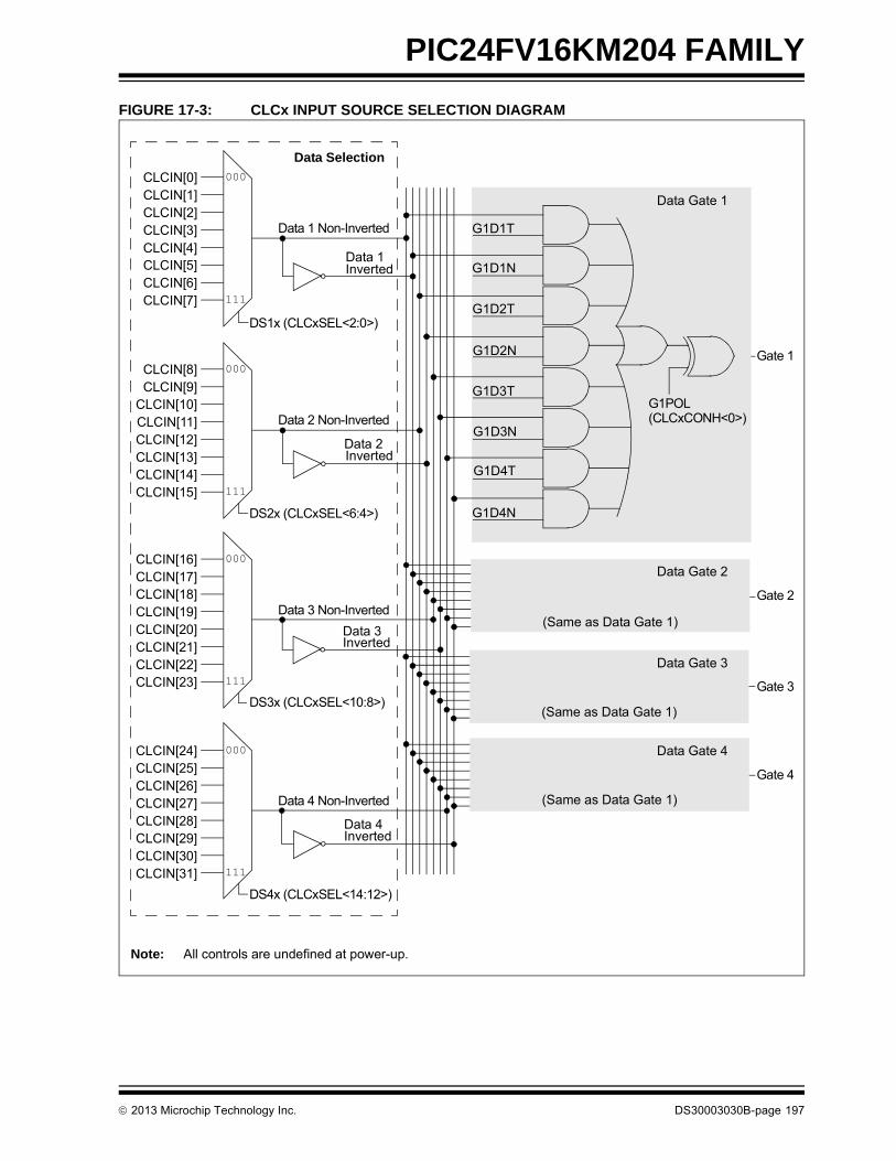
PIC24FV16KM204 FAMILY
FIGURE 17-3: CLCx INPUT SOURCE SELECTION DIAGRAM
Gate 1
G1POL
Data Gate 1
G1D1T
Gate 2
Gate 3
Gate 4
Data Gate 2
Data Gate 3
Data Gate 4
G1D1N
DS1x (CLCxSEL<2:0>)
DS2x (CLCxSEL<6:4>)
CLCIN[0]CLCIN[1]CLCIN[2]
CLCIN[5]CLCIN[6]CLCIN[7]
Data Selection
Note: All controls are undefined at power-up.
Data 1 Non-Inverted
Data 1
Data 2 Non-Inverted
Data 2
Data 3 Non-Inverted
Data 3
Data 4 Non-Inverted
Data 4
(Same as Data Gate 1)
(Same as Data Gate 1)
(Same as Data Gate 1)
G1D2T
G1D2N
G1D3T
G1D3N
G1D4T
G1D4N
Inverted
Inverted
Inverted
Inverted
CLCIN[8]CLCIN[9]
CLCIN[10]
CLCIN[13]CLCIN[14]CLCIN[15]
CLCIN[3]CLCIN[4]
CLCIN[11]CLCIN[12]
CLCIN[18]
CLCIN[21]CLCIN[22]CLCIN[23]
CLCIN[19]CLCIN[20]
CLCIN[17]CLCIN[16]
DS3x (CLCxSEL<10:8>)
CLCIN[26]
CLCIN[29]CLCIN[30]CLCIN[31]
CLCIN[27]CLCIN[28]
CLCIN[25]CLCIN[24]
DS4x (CLCxSEL<14:12>)
000
111
000
111
000
111
000
111
(CLCxCONH<0>)
2013 Microchip Technology Inc. DS30003030B-page 197

PIC24FV16KM204 FAMILY
17.1 Control Registers
The CLCx module is controlled by the following registers:
• CLCxCONL
• CLCxCONH
• CLCxSEL
• CLCxGLSL
• CLCxGLSH
The CLCx Control registers (CLCxCONL andCLCxCONH) are used to enable the module and inter-rupts, control the output enable bit, select output polarityand select the logic function. The CLCx Control registersalso allow the user to control the logic polarity of not onlythe cell output, but also some intermediate variables.
The CLCx Source Select register (CLCxSEL) allowsthe user to select up to 4 data input sources using the4 data input selection multiplexers. Each multiplexerhas a list of 8 data sources available.
The CLCx Gate Logic Select registers (CLCxGLSL andCLCxGLSH) allow the user to select which outputsfrom each of the selection MUXes are used as inputs tothe input gates of the logic cell. Each data source MUXoutputs both a true and a negated version of its output.All of these 8 signals are enabled, ORed together bythe logic cell input gates.
REGISTER 17-1: CLCxCONL: CLCx CONTROL REGISTER (LOW)
R/W-0 U-0 U-0 U-0 R/W-0 R/W-0 U-0 U-0
LCEN — — — INTP INTN — —
bit 15 bit 8
R-0 R-0 R/W-0 U-0 U-0 R/W-0 R/W-0 R/W-0
LCOE LCOUT LCPOL — — MODE2 MODE1 MODE0
bit 7 bit 0
Legend:
R = Readable bit W = Writable bit U = Unimplemented bit, read as ‘0’
-n = Value at POR ‘1’ = Bit is set ‘0’ = Bit is cleared x = Bit is unknown
bit 15 LCEN: CLCx Enable bit
1 = CLCx is enabled and mixing input signals0 = CLCx is disabled and has logic zero outputs
bit 14-12 Unimplemented: Read as ‘0’
bit 11 INTP: CLCx Positive Edge Interrupt Enable bit
1 = Interrupt will be generated when a rising edge occurs on LCOUT0 = Interrupt will not be generated
bit 10 INTN: CLCx Negative Edge Interrupt Enable bit
1 = Interrupt will be generated when a falling edge occurs on LCOUT0 = Interrupt will not be generated
bit 9-8 Unimplemented: Read as ‘0’
bit 7 LCOE: CLCx Port Enable bit
1 = CLCx port pin output is enabled0 = CLCx port pin output is disabled
bit 6 LCOUT: CLCx Data Output Status bit
1 = CLCx output high0 = CLCx output low
bit 5 LCPOL: CLCx Output Polarity Control bit
1 = The output of the module is inverted0 = The output of the module is not inverted
bit 4-3 Unimplemented: Read as ‘0’
DS30003030B-page 198 2013 Microchip Technology Inc.

PIC24FV16KM204 FAMILY
bit 2-0 MODE<2:0>: CLCx Mode bits
111 = Cell is a 1-input transparent latch with S and R110 = Cell is a JK flip-flop with R101 = Cell is a 2-input D flip-flop with R100 = Cell is a 1-input D flip-flop with S and R011 = Cell is an SR latch010 = Cell is a 4-input AND001 = Cell is an OR-XOR000 = Cell is a AND-OR
REGISTER 17-1: CLCxCONL: CLCx CONTROL REGISTER (LOW) (CONTINUED)
REGISTER 17-2: CLCxCONH: CLCx CONTROL REGISTER (HIGH)
U-0 U-0 U-0 U-0 U-0 U-0 U-0 U-0
— — — — — — — —
bit 15 bit 8
U-0 U-0 U-0 U-0 R/W-0 R/W-0 R/W-0 R/W-0
— — — — G4POL G3POL G2POL G1POL
bit 7 bit 0
Legend:
R = Readable bit W = Writable bit U = Unimplemented bit, read as ‘0’
-n = Value at POR ‘1’ = Bit is set ‘0’ = Bit is cleared x = Bit is unknown
bit 15-4 Unimplemented: Read as ‘0’
bit 3 G4POL: Gate 4 Polarity Control bit
1 = The output of Channel 4 logic is inverted when applied to the logic cell0 = The output of Channel 4 logic is not inverted
bit 2 G3POL: Gate 3 Polarity Control bit
1 = The output of Channel 3 logic is inverted when applied to the logic cell0 = The output of Channel 3 logic is not inverted
bit 1 G2POL: Gate 2 Polarity Control bit
1 = The output of Channel 2 logic is inverted when applied to the logic cell0 = The output of Channel 2 logic is not inverted
bit 0 G1POL: Gate 1 Polarity Control bit
1 = The output of Channel 1 logic is inverted when applied to the logic cell0 = The output of Channel 1 logic is not inverted
2013 Microchip Technology Inc. DS30003030B-page 199

PIC24FV16KM204 FAMILY
REGISTER 17-3: CLCxSEL: CLCx INPUT MUX SELECT REGISTER
U-0 R/W-0 R/W-0 R/W-0 U-0 R/W-0 R/W-0 R/W-0
— DS42 DS41 DS40 — DS32 DS31 DS30
bit 15 bit 8
U-0 R/W-0 R/W-0 R/W-0 U-0 R/W-0 R/W-0 R/W-0
— DS22 DS21 DS20 — DS12 DS11 DS10
bit 7 bit 0
Legend:
R = Readable bit W = Writable bit U = Unimplemented bit, read as ‘0’
-n = Value at POR ‘1’ = Bit is set ‘0’ = Bit is cleared x = Bit is unknown
bit 15 Unimplemented: Read as ‘0’
bit 14-12 DS4<2:0>: Data Selection MUX 4 Signal Selection bits
111 = MCCP3 Compare Event Flag (CCP3IF)110 = MCCP1 Compare Event Flag (CCP1IF)101 = Digital logic low100 = CTMU Trigger interrupt
For CLC1:011 = SPI1 SDIx010 = Comparator 3 output001 = CLC2 output000 = CLCINB I/O pin
For CLC2:011 = SPI2 SDIx010 = Comparator 3 output001 = CLC1 output000 = CLCINB I/O pin
bit 11 Unimplemented: Read as ‘0’
bit 10-8 DS3<2:0>: Data Selection MUX 3 Signal Selection bits
111 = MCCP3 Compare Event Flag (CCP3IF)110 = MCCP2 Compare Event Flag (CCP2IF)101 = Digital logic low
For CLC1:100 = UART1 RX011 = SPI1 SDOx010 = Comparator 2 output001 = CLC1 output000 = CLCINA I/O pin
For CLC2:100 = UART2 RX011 = SPI2 SDOx010 = Comparator 2 output001 = CLC2 output000 = CLCINA I/O pin
bit 7 Unimplemented: Read as ‘0’
DS30003030B-page 200 2013 Microchip Technology Inc.

PIC24FV16KM204 FAMILY
bit 6-4 DS2<2:0>: Data Selection MUX 2 Signal Selection bits
111 = MCCP2 Compare Event Flag (CCP2IF)110 = MCCP1 Compare Event Flag (CCP1IF)101 = Digital logic low100 = A/D end of conversion event
For CLC1:011 = UART1 TX010 = Comparator 1 output001 = CLC2 output000 = CLCINB I/O pin
For CLC2:011 = UART2 TX010 = Comparator 1 output001 = CLC1 output000 = CLCINB I/O pin
bit 3 Unimplemented: Read as ‘0’
bit 2-0 DS1<2:0>: Data Selection MUX 1 Signal Selection bits
111 = SCCP5 Compare Event Flag (CCP5IF)110 = SCCP4 Compare Event Flag (CCP4IF)101 = Digital logic low100 = 8 MHz FRC clock source011 = LPRC clock source010 = SOSC clock source001 = System clock (TCY)000 = CLCINA I/O pin
REGISTER 17-3: CLCxSEL: CLCx INPUT MUX SELECT REGISTER (CONTINUED)
2013 Microchip Technology Inc. DS30003030B-page 201

PIC24FV16KM204 FAMILY
REGISTER 17-4: CLCxGLSL: CLCx GATE LOGIC INPUT SELECT LOW REGISTER
R/W-0 R/W-0 R/W-0 R/W-0 R/W-0 R/W-0 R/W-0 R/W-0
G2D4T G2D4N G2D3T G2D3N G2D2T G2D2N G2D1T G2D1N
bit 15 bit 8
R/W-0 R/W-0 R/W-0 R/W-0 R/W-0 R/W-0 R/W-0 R/W-0
G1D4T G1D4N G1D3T G1D3N G1D2T G1D2N G1D1T G1D1N
bit 7 bit 0
Legend:
R = Readable bit W = Writable bit U = Unimplemented bit, read as ‘0’
-n = Value at POR ‘1’ = Bit is set ‘0’ = Bit is cleared x = Bit is unknown
bit 15 G2D4T: Gate 2 Data Source 4 True Enable bit
1 = The Data Source 4 inverted signal is enabled for Gate 20 = The Data Source 4 inverted signal is disabled for Gate 2
bit 14 G2D4N: Gate 2 Data Source 4 Negated Enable bit
1 = The Data Source 4 inverted signal is enabled for Gate 20 = The Data Source 4 inverted signal is disabled for Gate 2
bit 13 G2D3T: Gate 2 Data Source 3 True Enable bit
1 = The Data Source 3 inverted signal is enabled for Gate 20 = The Data Source 3 inverted signal is disabled for Gate 2
bit 12 G2D3N: Gate 2 Data Source 3 Negated Enable bit
1 = The Data Source 3 inverted signal is enabled for Gate 20 = The Data Source 3 inverted signal is disabled for Gate 2
bit 11 G2D2T: Gate 2 Data Source 2 True Enable bit
1 = The Data Source 2 inverted signal is enabled for Gate 20 = The Data Source 2 inverted signal is disabled for Gate 2
bit 10 G2D2N: Gate 2 Data Source 2 Negated Enable bit
1 = The Data Source 2 inverted signal is enabled for Gate 20 = The Data Source 2 inverted signal is disabled for Gate 2
bit 9 G2D1T: Gate 2 Data Source 1 True Enable bit
1 = The Data Source 1 inverted signal is enabled for Gate 20 = The Data Source 1 inverted signal is disabled for Gate 2
bit 8 G2D1N: Gate 2 Data Source 1 Negated Enable bit
1 = The Data Source 2 inverted signal is enabled for Gate 10 = The Data Source 2 inverted signal is disabled for Gate 1
bit 7 G1D4T: Gate 1 Data Source 4 True Enable bit
1 = The Data Source 4 inverted signal is enabled for Gate 10 = The Data Source 4 inverted signal is disabled for Gate 1
bit 6 G1D4N: Gate 1 Data Source 4 Negated Enable bit
1 = The Data Source 4 inverted signal is enabled for Gate 10 = The Data Source 4 inverted signal is disabled for Gate 1
bit 5 G1D3T: Gate 1 Data Source 3 True Enable bit
1 = The Data Source 3 inverted signal is enabled for Gate 10 = The Data Source 3 inverted signal is disabled for Gate 1
bit 4 G1D3N: Gate 1 Data Source 3 Negated Enable bit
1 = The Data Source 3 inverted signal is enabled for Gate 10 = The Data Source 3 inverted signal is disabled for Gate 1
DS30003030B-page 202 2013 Microchip Technology Inc.
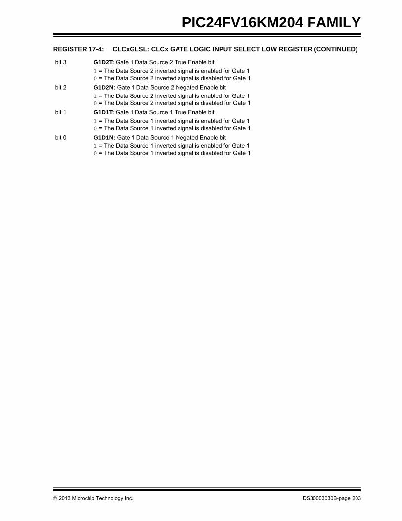
PIC24FV16KM204 FAMILY
bit 3 G1D2T: Gate 1 Data Source 2 True Enable bit
1 = The Data Source 2 inverted signal is enabled for Gate 10 = The Data Source 2 inverted signal is disabled for Gate 1
bit 2 G1D2N: Gate 1 Data Source 2 Negated Enable bit
1 = The Data Source 2 inverted signal is enabled for Gate 10 = The Data Source 2 inverted signal is disabled for Gate 1
bit 1 G1D1T: Gate 1 Data Source 1 True Enable bit
1 = The Data Source 1 inverted signal is enabled for Gate 10 = The Data Source 1 inverted signal is disabled for Gate 1
bit 0 G1D1N: Gate 1 Data Source 1 Negated Enable bit
1 = The Data Source 1 inverted signal is enabled for Gate 10 = The Data Source 1 inverted signal is disabled for Gate 1
REGISTER 17-4: CLCxGLSL: CLCx GATE LOGIC INPUT SELECT LOW REGISTER (CONTINUED)
2013 Microchip Technology Inc. DS30003030B-page 203

PIC24FV16KM204 FAMILY
REGISTER 17-5: CLCxGLSH: CLCx GATE LOGIC INPUT SELECT HIGH REGISTERR/W-0 R/W-0 R/W-0 R/W-0 R/W-0 R/W-0 R/W-0 R/W-0
G4D4T G4D4N G4D3T G4D3N G4D2T G4D2N G4D1T G4D1N
bit 15 bit 8
R/W-0 R/W-0 R/W-0 R/W-0 R/W-0 R/W-0 R/W-0 R/W-0
G3D4T G3D4N G3D3T G3D3N G3D2T G3D2N G3D1T G3D1N
bit 7 bit 0
Legend:
R = Readable bit W = Writable bit U = Unimplemented bit, read as ‘0’
-n = Value at POR ‘1’ = Bit is set ‘0’ = Bit is cleared x = Bit is unknown
bit 15 G4D4T: Gate 4 Data Source 4 True Enable bit
1 = The Data Source 4 inverted signal is enabled for Gate 40 = The Data Source 4 inverted signal is disabled for Gate 4
bit 14 G4D4N: Gate 4 Data Source 4 Negated Enable bit
1 = The Data Source 4 inverted signal is enabled for Gate 40 = The Data Source 4 inverted signal is disabled for Gate 4
bit 13 G4D3T: Gate 4 Data Source 3 True Enable bit
1 = The Data Source 3 inverted signal is enabled for Gate 40 = The Data Source 3 inverted signal is disabled for Gate 4
bit 12 G4D3N: Gate 4 Data Source 3 Negated Enable bit
1 = The Data Source 3 inverted signal is enabled for Gate 40 = The Data Source 3 inverted signal is disabled for Gate 4
bit 11 G4D2T: Gate 4 Data Source 2 True Enable bit
1 = The Data Source 2 inverted signal is enabled for Gate 40 = The Data Source 2 inverted signal is disabled for Gate 4
bit 10 G4D2N: Gate 4 Data Source 2 Negated Enable bit
1 = The Data Source 2 inverted signal is enabled for Gate 40 = The Data Source 2 inverted signal is disabled for Gate 4
bit 9 G4D1T: Gate 4 Data Source 1 True Enable bit
1 = The Data Source 1 inverted signal is enabled for Gate 40 = The Data Source 1 inverted signal is disabled for Gate 4
bit 8 G4D1N: Gate 4 Data Source 1 Negated Enable bit
1 = The Data Source 1 inverted signal is enabled for Gate 40 = The Data Source 1 inverted signal is disabled for Gate 4
bit 7 G3D4T: Gate 3 Data Source 4 True Enable bit
1 = The Data Source 4 inverted signal is enabled for Gate 30 = The Data Source 4 inverted signal is disabled for Gate 3
bit 6 G3D4N: Gate 3 Data Source 4 Negated Enable bit
1 = The Data Source 4 inverted signal is enabled for Gate 30 = The Data Source 4 inverted signal is disabled for Gate 3
bit 5 G3D3T: Gate 3 Data Source 3 True Enable bit
1 = The Data Source 3 inverted signal is enabled for Gate 30 = The Data Source 3 inverted signal is disabled for Gate 3
bit 4 G3D3N: Gate 3 Data Source 3 Negated Enable bit
1 = The Data Source 3 inverted signal is enabled for Gate 30 = The Data Source 3 inverted signal is disabled for Gate 3
DS30003030B-page 204 2013 Microchip Technology Inc.

PIC24FV16KM204 FAMILY
bit 3 G3D2T: Gate 3 Data Source 2 True Enable bit
1 = The Data Source 2 inverted signal is enabled for Gate 30 = The Data Source 2 inverted signal is disabled for Gate 3
bit 2 G3D2N: Gate 3 Data Source 2 Negated Enable bit
1 = The Data Source 2 inverted signal is enabled for Gate 30 = The Data Source 2 inverted signal is disabled for Gate 3
bit 1 G3D1T: Gate 3 Data Source 1 True Enable bit
1 = The Data Source 1 inverted signal is enabled for Gate 30 = The Data Source 1 inverted signal is disabled for Gate 3
bit 0 G3D1N: Gate 3 Data Source 1 Negated Enable bit
1 = The Data Source 1 inverted signal is enabled for Gate 30 = The Data Source 1 inverted signal is disabled for Gate 3
REGISTER 17-5: CLCxGLSH: CLCx GATE LOGIC INPUT SELECT HIGH REGISTER (CONTINUED)
2013 Microchip Technology Inc. DS30003030B-page 205

PIC24FV16KM204 FAMILY
NOTES:
DS30003030B-page 206 2013 Microchip Technology Inc.

PIC24FV16KM204 FAMILY
18.0 HIGH/LOW-VOLTAGE DETECT (HLVD)
The High/Low-Voltage Detect module (HLVD) is aprogrammable circuit that allows the user to specifyboth the device voltage trip point and the direction ofchange.
An interrupt flag is set if the device experiences anexcursion past the trip point in the direction of change.If the interrupt is enabled, the program execution willbranch to the interrupt vector address and the softwarecan then respond to the interrupt.
The HLVD Control register (see Register 18-1) com-pletely controls the operation of the HLVD module. Thisallows the circuitry to be “turned off” by the user undersoftware control, which minimizes the currentconsumption for the device.
FIGURE 18-1: HIGH/LOW-VOLTAGE DETECT (HLVD) MODULE BLOCK DIAGRAM
Note: This data sheet summarizes the features ofthis group of PIC24F devices. It is notintended to be a comprehensive referencesource. For more information onthe High/Low-Voltage Detect, refer tothe “PIC24F Family Reference Manual”,“High-Level Integration withProgrammable High/Low-VoltageDetect (HLVD)” (DS39725).
Set
VDD
16
-to
-1 M
UX
HLVDEN
HLVDL<3:0>HLVDIN
VDD
Externally GeneratedTrip Point
HLVDIF
HLVDEN
Internal VoltageReference
VDIR
VBG
–
2013 Microchip Technology Inc. DS30003030B-page 207

PIC24FV16KM204 FAMILY
REGISTER 18-1: HLVDCON: HIGH/LOW-VOLTAGE DETECT CONTROL REGISTER
R/W-0 U-0 R/W-0 U-0 U-0 U-0 U-0 U-0
HLVDEN — HLSIDL — — — — —
bit 15 bit 8
R/W-0 R/W-0 R/W-0 U-0 R/W-0 R/W-0 R/W-0 R/W-0
VDIR BGVST IRVST — HLVDL3 HLVDL2 HLVDL1 HLVDL0
bit 7 bit 0
Legend:
R = Readable bit W = Writable bit U = Unimplemented bit, read as ‘0’
-n = Value at POR ‘1’ = Bit is set ‘0’ = Bit is cleared x = Bit is unknown
bit 15 HLVDEN: High/Low-Voltage Detect Power Enable bit
1 = HLVD is enabled0 = HLVD is disabled
bit 14 Unimplemented: Read as ‘0’
bit 13 HLSIDL: HLVD Stop in Idle Mode bit
1 = Discontinues module operation when device enters Idle mode0 = Continues module operation in Idle mode
bit 12-8 Unimplemented: Read as ‘0’
bit 7 VDIR: Voltage Change Direction Select bit
1 = Event occurs when voltage equals or exceeds trip point (HLVDL<3:0>)0 = Event occurs when voltage equals or falls below trip point (HLVDL<3:0>)
bit 6 BGVST: Band Gap Voltage Stable Flag bit
1 = Indicates that the band gap voltage is stable0 = Indicates that the band gap voltage is unstable
bit 5 IRVST: Internal Reference Voltage Stable Flag bit
1 = Indicates that the internal reference voltage is stable and the High-Voltage Detect logic generatesthe interrupt flag at the specified voltage range
0 = Indicates that the internal reference voltage is unstable and the High-Voltage Detect logic will notgenerate the interrupt flag at the specified voltage range, and the HLVD interrupt should not beenabled
bit 4 Unimplemented: Read as ‘0’
bit 3-0 HLVDL<3:0>: High/Low-Voltage Detection Limit bits
1111 = External analog input is used (input comes from the HLVDIN pin)1110 = Trip Point 1(1)
1101 = Trip Point 2(1)
1100 = Trip Point 3(1)
.
.
.0000 = Trip Point 15(1)
Note 1: For the actual trip point, see Section 27.0 “Electrical Characteristics”.
DS30003030B-page 208 2013 Microchip Technology Inc.

PIC24FV16KM204 FAMILY
19.0 12-BIT A/D CONVERTER WITH THRESHOLD DETECT
The PIC24F 12-bit A/D Converter has the following keyfeatures:
• Successive Approximation Register (SAR) Conversion
• Conversion Speeds of up to 100 ksps
• Up to 32 Analog Input Channels (internal and external)
• Multiple Internal Reference Input Channels
• External Voltage Reference Input Pins
• Unipolar Differential Sample-and-Hold (S/H) Amplifier
• Automated Threshold Scan and Compare Operation to Pre-Evaluate Conversion Results
• Selectable Conversion Trigger Source
• Fixed-Length (one word per channel), Configurable Conversion Result Buffer
• Four Options for Results Alignment
• Configurable Interrupt Generation
• Operation During CPU Sleep and Idle modes
The 12-bit A/D Converter module is an enhancedversion of the 10-bit module offered in some PIC24devices. Both modules are Successive ApproximationRegister (SAR) converters at their cores, surroundedby a range of hardware features for flexibleconfiguration. This version of the module extendsfunctionality by providing 12-bit resolution, a widerrange of automatic sampling options and tighterintegration with other analog modules, such as theCTMU, and a configurable results buffer. There is alegacy 10-bit mode on this A/D to allow the option to runwith lower resolution in order to obtain higherthroughput. This module also includes a uniqueThreshold Detect feature that allows the module itselfto make simple decisions based on the conversionresults.
A simplified block diagram for the module is illustratedin Figure 19-1.
Note: This data sheet summarizes the features ofthis group of PIC24F devices. It is notintended to be a comprehensive referencesource. For more information on the 12-BitA/D Converter with Threshold Detect, referto the “PIC24F Family Reference Manual”,“12-Bit A/D Converter with ThresholdDetect” (DS39739).
2013 Microchip Technology Inc. DS30003030B-page 209

PIC24FV16KM204 FAMILY
FIGURE 19-1: 12-BIT A/D CONVERTER BLOCK DIAGRAM
Comparator
10/12-Bit SAR
VREF+
DAC
AN20
AN21
AN8
AN9
AN4
AN5
AN6
AN7
AN0
AN1
AN2
AN3
VREF-
Sample Control
S/H
AVSS
AVDD
ADC1BUF0:ADC1BUF17
AD1CON1
AD1CON2
AD1CON3
AD1CHS
AD1CHITL
AD1CHITH
Control Logic
Data Formatting
Input MUX Control
Conversion Control
Pin Config. Control
Internal
16
VR+VR-M
UX
A
VINH
VINL
VINH
VINH
VINL
VINL
VR+
VR-V
R S
ele
ct
CTMU
VBG
AD1CSSL
AD1CSSH
AVss
0.785 * VDD
AVDD
0.215 * VDD
AD1CON5
CTMU
VBG
Temp. Sensor
Data Bus
MU
X B
Conversion Logic
DS30003030B-page 210 2013 Microchip Technology Inc.
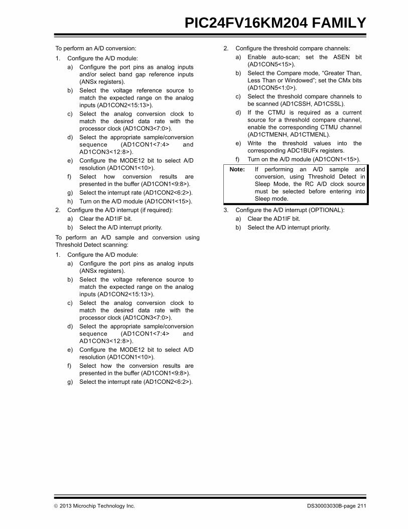
PIC24FV16KM204 FAMILY
To perform an A/D conversion:
1. Configure the A/D module:
a) Configure the port pins as analog inputsand/or select band gap reference inputs(ANSx registers).
b) Select the voltage reference source tomatch the expected range on the analoginputs (AD1CON2<15:13>).
c) Select the analog conversion clock tomatch the desired data rate with theprocessor clock (AD1CON3<7:0>).
d) Select the appropriate sample/conversionsequence (AD1CON1<7:4> andAD1CON3<12:8>).
e) Configure the MODE12 bit to select A/Dresolution (AD1CON1<10>).
f) Select how conversion results arepresented in the buffer (AD1CON1<9:8>).
g) Select the interrupt rate (AD1CON2<6:2>).
h) Turn on the A/D module (AD1CON1<15>).
2. Configure the A/D interrupt (if required):
a) Clear the AD1IF bit.
b) Select the A/D interrupt priority.
To perform an A/D sample and conversion usingThreshold Detect scanning:
1. Configure the A/D module:
a) Configure the port pins as analog inputs(ANSx registers).
b) Select the voltage reference source tomatch the expected range on the analoginputs (AD1CON2<15:13>).
c) Select the analog conversion clock tomatch the desired data rate with theprocessor clock (AD1CON3<7:0>).
d) Select the appropriate sample/conversionsequence (AD1CON1<7:4> andAD1CON3<12:8>).
e) Configure the MODE12 bit to select A/Dresolution (AD1CON1<10>).
f) Select how the conversion results arepresented in the buffer (AD1CON1<9:8>).
g) Select the interrupt rate (AD1CON2<6:2>).
2. Configure the threshold compare channels:
a) Enable auto-scan; set the ASEN bit(AD1CON5<15>).
b) Select the Compare mode, “Greater Than,Less Than or Windowed”; set the CMx bits(AD1CON5<1:0>).
c) Select the threshold compare channels tobe scanned (AD1CSSH, AD1CSSL).
d) If the CTMU is required as a currentsource for a threshold compare channel,enable the corresponding CTMU channel(AD1CTMENH, AD1CTMENL).
e) Write the threshold values into thecorresponding ADC1BUFx registers.
f) Turn on the A/D module (AD1CON1<15>).
3. Configure the A/D interrupt (OPTIONAL):
a) Clear the AD1IF bit.
b) Select the A/D interrupt priority.
Note: If performing an A/D sample andconversion, using Threshold Detect inSleep Mode, the RC A/D clock sourcemust be selected before entering intoSleep mode.
2013 Microchip Technology Inc. DS30003030B-page 211
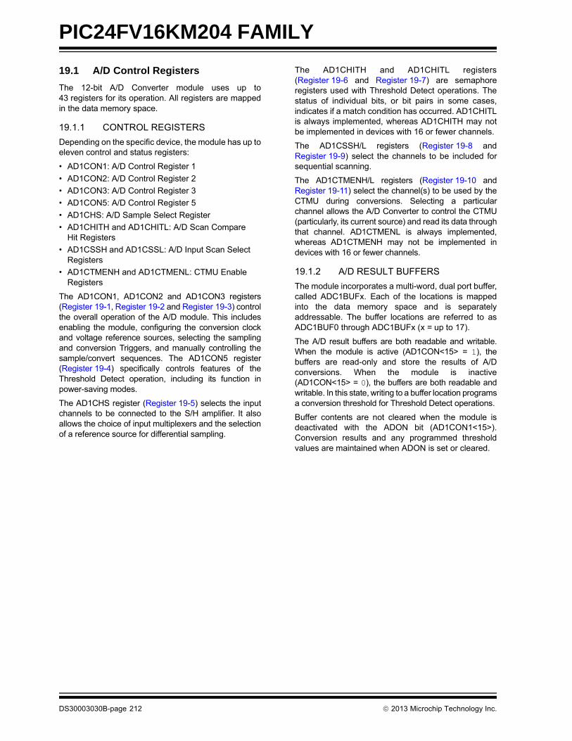
PIC24FV16KM204 FAMILY
19.1 A/D Control Registers
The 12-bit A/D Converter module uses up to43 registers for its operation. All registers are mappedin the data memory space.
19.1.1 CONTROL REGISTERS
Depending on the specific device, the module has up toeleven control and status registers:
• AD1CON1: A/D Control Register 1
• AD1CON2: A/D Control Register 2
• AD1CON3: A/D Control Register 3
• AD1CON5: A/D Control Register 5
• AD1CHS: A/D Sample Select Register
• AD1CHITH and AD1CHITL: A/D Scan Compare Hit Registers
• AD1CSSH and AD1CSSL: A/D Input Scan Select Registers
• AD1CTMENH and AD1CTMENL: CTMU Enable Registers
The AD1CON1, AD1CON2 and AD1CON3 registers(Register 19-1, Register 19-2 and Register 19-3) controlthe overall operation of the A/D module. This includesenabling the module, configuring the conversion clockand voltage reference sources, selecting the samplingand conversion Triggers, and manually controlling thesample/convert sequences. The AD1CON5 register(Register 19-4) specifically controls features of theThreshold Detect operation, including its function inpower-saving modes.
The AD1CHS register (Register 19-5) selects the inputchannels to be connected to the S/H amplifier. It alsoallows the choice of input multiplexers and the selectionof a reference source for differential sampling.
The AD1CHITH and AD1CHITL registers(Register 19-6 and Register 19-7) are semaphoreregisters used with Threshold Detect operations. Thestatus of individual bits, or bit pairs in some cases,indicates if a match condition has occurred. AD1CHITLis always implemented, whereas AD1CHITH may notbe implemented in devices with 16 or fewer channels.
The AD1CSSH/L registers (Register 19-8 andRegister 19-9) select the channels to be included forsequential scanning.
The AD1CTMENH/L registers (Register 19-10 andRegister 19-11) select the channel(s) to be used by theCTMU during conversions. Selecting a particularchannel allows the A/D Converter to control the CTMU(particularly, its current source) and read its data throughthat channel. AD1CTMENL is always implemented,whereas AD1CTMENH may not be implemented indevices with 16 or fewer channels.
19.1.2 A/D RESULT BUFFERS
The module incorporates a multi-word, dual port buffer,called ADC1BUFx. Each of the locations is mappedinto the data memory space and is separatelyaddressable. The buffer locations are referred to asADC1BUF0 through ADC1BUFx (x = up to 17).
The A/D result buffers are both readable and writable.When the module is active (AD1CON<15> = 1), thebuffers are read-only and store the results of A/Dconversions. When the module is inactive(AD1CON<15> = 0), the buffers are both readable andwritable. In this state, writing to a buffer location programsa conversion threshold for Threshold Detect operations.
Buffer contents are not cleared when the module isdeactivated with the ADON bit (AD1CON1<15>).Conversion results and any programmed thresholdvalues are maintained when ADON is set or cleared.
DS30003030B-page 212 2013 Microchip Technology Inc.

PIC24FV16KM204 FAMILY
REGISTER 19-1: AD1CON1: A/DA/D CONTROL REGISTER 1
R/W-0 U-0 R/W-0 U-0 U-0 R/W-0 R/W-0 R/W-0
ADON — ADSIDL — — MODE12 FORM1 FORM0
bit 15 bit 8
R/W-0 R/W-0 R/W-0 R/W-0 U-0 R/W-0 R/W-0, HSC R/C-0, HSC
SSRC3 SSRC2 SSRC1 SSRC0 — ASAM SAMP DONE
bit 7 bit 0
Legend: C = Clearable bit U = Unimplemented bit, read as ‘0’
R = Readable bit W = Writable bit HSC = Hardware Settable/Clearable bit
-n = Value at POR ‘1’ = Bit is set ‘0’ = Bit is cleared x = Bit is unknown
bit 15 ADON: A/D Operating Mode bit
1 = A/D Converter is operating0 = A/D Converter is off
bit 14 Unimplemented: Read as ‘0’
bit 13 ADSIDL: A/D Stop in Idle Mode bit
1 = Discontinues module operation when device enters Idle mode0 = Continues module operation in Idle mode
bit 12-11 Unimplemented: Read as ‘0’
bit 10 MODE12: 12-Bit A/D Operation Mode bit
1 = 12-bit A/D operation0 = 10-bit A/D operation
bit 9-8 FORM<1:0>: Data Output Format bits (see the following formats)
11 = Fractional result, signed, left justified10 = Absolute fractional result, unsigned, left justified01 = Decimal result, signed, right justified00 = Absolute decimal result, unsigned, right justified
bit 7-4 SSRC<3:0>: Sample Clock Source Select bits
1111 = Reserved•••1101 = Reserved1100 = CLC2 event ends sampling and starts conversion1011 = SCCP4 Compare Event (CCP4IF) ends sampling and starts conversion1010 = MCCP3 Compare Event (CCP3IF) ends sampling and starts conversion1001 = MCCP2 Compare Event (CCP2IF) ends sampling and starts conversion1000 = CLC1 event ends sampling and starts conversion0111 = Internal counter ends sampling and starts conversion (auto-convert)0110 = TMR1 Sleep mode Trigger event ends sampling and starts conversion(1)
0101 = TMR1 event ends sampling and starts conversion0100 = CTMU event ends sampling and starts conversion0011 = SCCP5 Compare Event (CCP5IF) ends sampling and starts conversion0010 = MCCP1 Compare Event (CCP1IF) ends sampling and starts conversion0001 = INT0 event ends sampling and starts conversion0000 = Clearing the Sample bit ends sampling and starts conversion
Note 1: This version of the TMR1 Trigger allows A/D conversions to be triggered from TMR1 while the device is operating in Sleep mode. The SSRC<3:0> = 0101 option allows conversions to be triggered in Run or Idle modes only.
2013 Microchip Technology Inc. DS30003030B-page 213
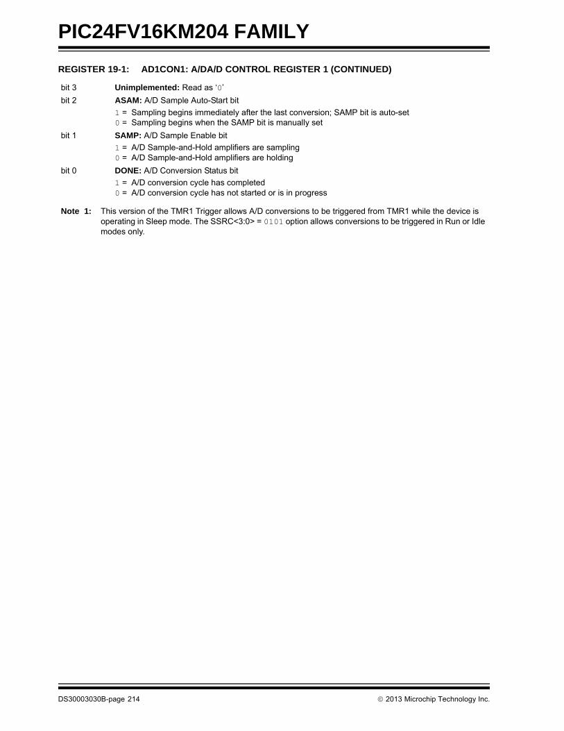
PIC24FV16KM204 FAMILY
bit 3 Unimplemented: Read as ‘0’
bit 2 ASAM: A/D Sample Auto-Start bit
1 = Sampling begins immediately after the last conversion; SAMP bit is auto-set0 = Sampling begins when the SAMP bit is manually set
bit 1 SAMP: A/D Sample Enable bit
1 = A/D Sample-and-Hold amplifiers are sampling0 = A/D Sample-and-Hold amplifiers are holding
bit 0 DONE: A/D Conversion Status bit
1 = A/D conversion cycle has completed 0 = A/D conversion cycle has not started or is in progress
REGISTER 19-1: AD1CON1: A/DA/D CONTROL REGISTER 1 (CONTINUED)
Note 1: This version of the TMR1 Trigger allows A/D conversions to be triggered from TMR1 while the device is operating in Sleep mode. The SSRC<3:0> = 0101 option allows conversions to be triggered in Run or Idle modes only.
DS30003030B-page 214 2013 Microchip Technology Inc.

PIC24FV16KM204 FAMILY
REGISTER 19-2: AD1CON2: A/D CONTROL REGISTER 2
R/W-0 R/W-0 R/W-0 U-0 R/W-0 R/W-0 U-0 U-0
PVCFG1 PVCFG0 NVCFG0 — BUFREGEN CSCNA — —
bit 15 bit 8
R/W-0 R/W-0 R/W-0 R/W-0 R/W-0 R/W-0 R/W-0 R/W-0
BUFS(1) SMPI4 SMPI3 SMPI2 SMPI1 SMPI0 BUFM(1) ALTS
bit 7 bit 0
Legend:
R = Readable bit W = Writable bit U = Unimplemented bit, read as ‘0’
-n = Value at POR ‘1’ = Bit is set ‘0’ = Bit is cleared x = Bit is unknown
bit 15-14 PVCFG<1:0>: A/D Converter Positive Voltage Reference Configuration bits
11 = 4 * Internal VBG(2)
10 = 2 * Internal VBG(3)
01 = External VREF+00 = AVDD
bit 13 NVCFG0: A/D Converter Negative Voltage Reference Configuration bits
1 = External VREF-0 = AVSS
bit 12 Unimplemented: Read as ‘0’
bit 11 BUFREGEN: A/D Buffer Register Enable bit
1 = Conversion result is loaded into a buffer location determined by the converted channel0 = A/D result buffer is treated as a FIFO
bit 10 CSCNA: Scan Input Selections for CH0+ S/H Input for MUX A Setting bit
1 = Scans inputs0 = Does not scan inputs
bit 9-8 Unimplemented: Read as ‘0’
bit 7 BUFS: A/D Buffer Fill Status bit(1)
1 = A/D is filling the upper half of the buffer; user should access data in the lower half0 = A/D is filling the lower half of the buffer; user should access data in the upper half
bit 6-2 SMPI<4:0>: Interrupt Sample Rate Select bits
11111 = Interrupts at the completion of the conversion for each 32nd sample11110 = Interrupts at the completion of the conversion for each 31st sample•••00001 = Interrupts at the completion of the conversion for every other sample00000 = Interrupts at the completion of the conversion for each sample
bit 1 BUFM: A/D Buffer Fill Mode Select bit(1)
1 = Starts filling the buffer at address, ADC1BUF0, on the first interrupt and ADC1BUF(x/2) on the nextinterrupt (Split Buffer mode)
0 = Starts filling the buffer at address, ADC1BUF0, and each sequential address on successiveinterrupts (FIFO mode)
bit 0 ALTS: Alternate Input Sample Mode Select bit
1 = Uses channel input selects for Sample A on the first sample and Sample B on the next sample0 = Always uses channel input selects for Sample A
Note 1: This is only applicable when the buffer is used in FIFO mode (BUFREGEN = 0). In addition, BUFS is only used when BUFM = 1.
2: PIC24FV16KMXXX devices only. Reference setting will not be within specification for VDD below 4.5V.3: Reference setting will not be within specification for VDD below 2.3V.
2013 Microchip Technology Inc. DS30003030B-page 215

PIC24FV16KM204 FAMILY
REGISTER 19-3: AD1CON3: A/D CONTROL REGISTER 3R/W-0 R-0 r-0 R/W-0 R/W-0 R/W-0 R/W-0 R/W-0
ADRC EXTSAM r SAMC4 SAMC3 SAMC2 SAMC1 SAMC0
bit 15 bit 8
R/W-0 R/W-0 R/W-0 R/W-0 R/W-0 R/W-0 R/W-0 R/W-0
ADCS7 ADCS6 ADCS5 ADCS4 ADCS3 ADCS2 ADCS1 ADCS0
bit 7 bit 0
Legend: r = Reserved bit
R = Readable bit W = Writable bit U = Unimplemented bit, read as ‘0’
-n = Value at POR ‘1’ = Bit is set ‘0’ = Bit is cleared x = Bit is unknown
bit 15 ADRC: A/D Conversion Clock Source bit
1 = RC clock0 = Clock is derived from the system clock
bit 14 EXTSAM: Extended Sampling Time bit
1 = A/D is still sampling after SAMP = 00 = A/D is finished sampling
bit 13 Reserved: Maintain as ‘0’
bit 12-8 SAMC<4:0>: Auto-Sample Time Select bits
11111 = 31 TAD
•••00001 = 1 TAD
00000 = 0 TAD
bit 7-0 ADCS<7:0>: A/D Conversion Clock Select bits
11111111-01000000 = Reserved 00111111 = 64 * TCY = TAD
•••00000001 = 2 * TCY = TAD
00000000 = TCY = TAD
DS30003030B-page 216 2013 Microchip Technology Inc.

PIC24FV16KM204 FAMILY
REGISTER 19-4: AD1CON5: A/D CONTROL REGISTER 5
R/W-0 R/W-0 R/W-0 R/W-0 r-0 U-0 R/W-0 R/W-0
ASEN(1) LPEN CTMREQ BGREQ r — ASINT1 ASINT0
bit 15 bit 8
U-0 U-0 U-0 U-0 R/W-0 R/W-0 R/W-0 R/W-0
— — — — WM1 WM0 CM1 CM0
bit 7 bit 0
Legend: r = Reserved bit
R = Readable bit W = Writable bit U = Unimplemented bit, read as ‘0’
-n = Value at POR ‘1’ = Bit is set ‘0’ = Bit is cleared x = Bit is unknown
bit 15 ASEN: A/D Auto-Scan Enable bit(1)
1 = Auto-scan is enabled0 = Auto-scan is disabled
bit 14 LPEN: A/D Low-Power Enable bit
1 = Returns to Low-Power mode after scan0 = Remains in Full-Power mode after scan
bit 13 CTMREQ: CTMU Request bit
1 = CTMU is enabled when the A/D is enabled and active0 = CTMU is not enabled by the A/D
bit 12 BGREQ: Band Gap Request bit
1 = Band gap is enabled when the A/D is enabled and active0 = Band gap is not enabled by the A/D
bit 11 Reserved: Maintain as ‘0’
bit 10 Unimplemented: Read as ‘0’
bit 9-8 ASINT<1:0>: Auto-Scan (Threshold Detect) Interrupt Mode bits
11 = Interrupt after a Threshold Detect sequence has completed and a valid compare has occurred10 = Interrupt after a valid compare has occurred01 = Interrupt after a Threshold Detect sequence has completed00 = No interrupt
bit 7-4 Unimplemented: Read as ‘0’
bit 3-2 WM<1:0>: A/D Write Mode bits
11 = Reserved10 = Auto-compare only (conversion results are not saved, but interrupts are generated when a valid
match, as defined by the CMx and ASINTx bits, occurs)01 = Convert and save (conversion results are saved to locations as determined by the register bits when
a match, as defined by the CMx bits, occurs)00 = Legacy operation (conversion data is saved to a location determined by the buffer register bits)
bit 1-0 CM<1:0>: A/D Compare Mode bits
11 = Outside Window mode (valid match occurs if the conversion result is outside of the window defined bythe corresponding buffer pair)
10 = Inside Window mode (valid match occurs if the conversion result is inside the window defined by thecorresponding buffer pair)
01 = Greater Than mode (valid match occurs if the result is greater than the value in the corresponding bufferregister)
00 = Less Than mode (valid match occurs if the result is less than the value in the corresponding buffer register)
Note 1: When using auto-scan with Threshold Detect (ASEN = 1), do not configure the sample clock source to Auto-Convert mode (SSRC<3:0> = 7). Any other available SSRC selection is valid. To use auto-convert as the sample clock source (SSRC<3:0> = 7), make sure ASEN is cleared.
2013 Microchip Technology Inc. DS30003030B-page 217
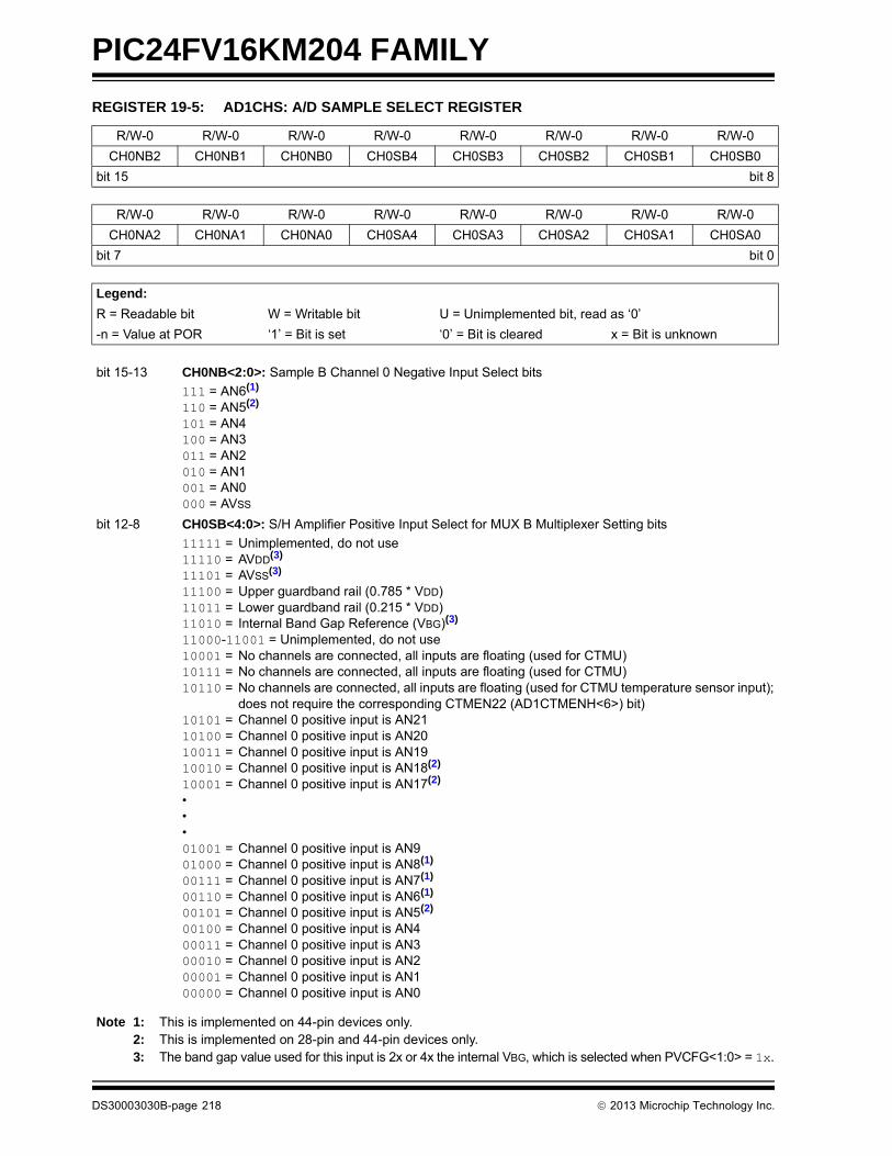
PIC24FV16KM204 FAMILY
REGISTER 19-5: AD1CHS: A/D SAMPLE SELECT REGISTER
R/W-0 R/W-0 R/W-0 R/W-0 R/W-0 R/W-0 R/W-0 R/W-0
CH0NB2 CH0NB1 CH0NB0 CH0SB4 CH0SB3 CH0SB2 CH0SB1 CH0SB0
bit 15 bit 8
R/W-0 R/W-0 R/W-0 R/W-0 R/W-0 R/W-0 R/W-0 R/W-0
CH0NA2 CH0NA1 CH0NA0 CH0SA4 CH0SA3 CH0SA2 CH0SA1 CH0SA0
bit 7 bit 0
Legend:
R = Readable bit W = Writable bit U = Unimplemented bit, read as ‘0’
-n = Value at POR ‘1’ = Bit is set ‘0’ = Bit is cleared x = Bit is unknown
bit 15-13 CH0NB<2:0>: Sample B Channel 0 Negative Input Select bits
111 = AN6(1)
110 = AN5(2)
101 = AN4100 = AN3011 = AN2010 = AN1001 = AN0000 = AVSS
bit 12-8 CH0SB<4:0>: S/H Amplifier Positive Input Select for MUX B Multiplexer Setting bits
11111 = Unimplemented, do not use11110 = AVDD(3)
11101 = AVSS(3)
11100 = Upper guardband rail (0.785 * VDD)11011 = Lower guardband rail (0.215 * VDD)11010 = Internal Band Gap Reference (VBG)(3)
11000-11001 = Unimplemented, do not use10001 = No channels are connected, all inputs are floating (used for CTMU)10111 = No channels are connected, all inputs are floating (used for CTMU)10110 = No channels are connected, all inputs are floating (used for CTMU temperature sensor input);
does not require the corresponding CTMEN22 (AD1CTMENH<6>) bit)10101 = Channel 0 positive input is AN2110100 = Channel 0 positive input is AN2010011 = Channel 0 positive input is AN1910010 = Channel 0 positive input is AN18(2)
10001 = Channel 0 positive input is AN17(2)
•••01001 = Channel 0 positive input is AN901000 = Channel 0 positive input is AN8(1)
00111 = Channel 0 positive input is AN7(1)
00110 = Channel 0 positive input is AN6(1)
00101 = Channel 0 positive input is AN5(2)
00100 = Channel 0 positive input is AN400011 = Channel 0 positive input is AN300010 = Channel 0 positive input is AN200001 = Channel 0 positive input is AN100000 = Channel 0 positive input is AN0
Note 1: This is implemented on 44-pin devices only.2: This is implemented on 28-pin and 44-pin devices only. 3: The band gap value used for this input is 2x or 4x the internal VBG, which is selected when PVCFG<1:0> = 1x.
DS30003030B-page 218 2013 Microchip Technology Inc.

PIC24FV16KM204 FAMILY
bit 7-5 CH0NA<2:0>: Sample A Channel 0 Negative Input Select bits
The same definitions as for CHONB<2:0>.
bit 4-0 CH0SA<4:0>: Sample A Channel 0 Positive Input Select bits
The same definitions as for CHONA<4:0>.
REGISTER 19-5: AD1CHS: A/D SAMPLE SELECT REGISTER (CONTINUED)
Note 1: This is implemented on 44-pin devices only.2: This is implemented on 28-pin and 44-pin devices only. 3: The band gap value used for this input is 2x or 4x the internal VBG, which is selected when PVCFG<1:0> = 1x.
REGISTER 19-6: AD1CHITH: A/D SCAN COMPARE HIT REGISTER (HIGH WORD)(1)
U-0 U-0 U-0 U-0 U-0 U-0 U-0 U-0
— — — — — — — —
bit 15 bit 8
R/W-0 R/W-0 R/W-0 R/W-0 R/W-0 R/W-0 R/W-0 R/W-0
CHH23 CHH22 CHH21 CHH20(2) CHH19(2) CHH18 CHH17 CHH16
bit 7 bit 0
Legend:
R = Readable bit W = Writable bit U = Unimplemented bit, read as ‘0’
-n = Value at POR ‘1’ = Bit is set ‘0’ = Bit is cleared x = Bit is unknown
bit 15-8 Unimplemented: Read as ‘0’.
bit 7-0 CHH<23:16>: A/D Compare Hit bits(2)
If CM<1:0> = 11:1 = A/D Result Buffer x has been written with data or a match has occurred0 = A/D Result Buffer x has not been written with data
For All Other Values of CM<1:0>:1 = A match has occurred on A/D Result Channel x0 = No match has occurred on A/D Result Channel x
Note 1: Unimplemented channels are read as ‘0’.
2: The CHH<20:19> bits are not implemented in 20-pin devices.
2013 Microchip Technology Inc. DS30003030B-page 219

PIC24FV16KM204 FAMILY
REGISTER 19-7: AD1CHITL: A/D SCAN COMPARE HIT REGISTER (LOW WORD)(1)
R/W-0 R/W-0 R/W-0 R/W-0 R/W-0 R/W-0 R/W-0 R/W-0
CHH15 CHH14 CHH13 CHH12 CHH11 CHH10 CHH9 CHH8(2,3)
bit 15 bit 8
R/W-0 R/W-0 R/W-0 R/W-0 R/W-0 R/W-0 R/W-0 R/W-0
CHH7(2,3) CHH6(2,3) CHH5(2) CHH4 CHH3 CHH2 CHH1 CHH0
bit 7 bit 0
Legend:
R = Readable bit W = Writable bit U = Unimplemented bit, read as ‘0’
-n = Value at POR ‘1’ = Bit is set ‘0’ = Bit is cleared x = Bit is unknown
bit 15-0 CHH<15:0>: A/D Compare Hit bits(2,3)
If CM<1:0> = 11:1 = A/D Result Buffer x has been written with data or a match has occurred0 = A/D Result Buffer x has not been written with data
For All Other Values of CM<1:0>:1 = A match has occurred on A/D Result Channel x0 = No match has occurred on A/D Result Channel x
Note 1: Unimplemented channels are read as ‘0’.
2: The CHH<8:5> bits are not implemented in 20-pin devices.
3: The CHH<8:6> bits are not implemented in 28-pin devices.
DS30003030B-page 220 2013 Microchip Technology Inc.

PIC24FV16KM204 FAMILY
REGISTER 19-8: AD1CSSH: A/D INPUT SCAN SELECT REGISTER (HIGH WORD)(1)
U-0 R/W-0 R/W-0 R/W-0 R/W-0 R/W-0 U-0 U-0
— CSS30 CSS29 CSS28 CSS27 CSS26 — —
bit 15 bit 8
R/W-0 R/W-0 R/W-0 R/W-0 R/W-0 R/W-0 R/W-0 R/W-0
CSS23 CSS22 CSS21 CSS20(2) CSS19(2) CSS18 CSS17 CSS16
bit 7 bit 0
Legend:
R = Readable bit W = Writable bit U = Unimplemented bit, read as ‘0’
-n = Value at POR ‘1’ = Bit is set ‘0’ = Bit is cleared x = Bit is unknown
bit 15 Unimplemented: Read as ‘0’
bit 14-10 CSS<30:26>: A/D Input Scan Selection bits
1 = Includes the corresponding channel for input scan0 = Skips the channel for input scan
bit 9-8 Unimplemented: Read as ‘0’
bit 7-0 CSS<23:16>: A/D Input Scan Selection bits(2)
1 = Includes the corresponding channel for input scan0 = Skips the channel for input scan
Note 1: Unimplemented channels are read as ‘0’. Do not select unimplemented channels for sampling as indeterminate results may be produced.
2: The CSS<20:19> bits are not implemented in 20-pin devices.
REGISTER 19-9: AD1CSSL: A/D INPUT SCAN SELECT REGISTER (LOW WORD)(1)
R/W-0 R/W-0 R/W-0 R/W-0 R/W-0 R/W-0 R/W-0 R/W-0
CSS15 CSS14 CSS13 CSS12 CSS11 CSS10 CSS9 CSS8(2,3)
bit 15 bit 8
R/W-0 R/W-0 R/W-0 R/W-0 R/W-0 R/W-0 R/W-0 R/W-0
CSS7(2,3) CSS6(2,3) CSS5(2) CSS4 CSS3 CSS2 CSS1 CSS0
bit 7 bit 0
Legend:
R = Readable bit W = Writable bit U = Unimplemented bit, read as ‘0’
-n = Value at POR ‘1’ = Bit is set ‘0’ = Bit is cleared x = Bit is unknown
bit 15-0 CSS<15:0>: A/D Input Scan Selection bits(2,3)
1 = Includes the corresponding ANx input for scan0 = Skips the channel for input scan
Note 1: Unimplemented channels are read as ‘0’. Do not select unimplemented channels for sampling as indeterminate results may be produced.
2: The CSS<8:5> bits are not implemented in 20-pin devices.
3: The CSS<8:6> bits are not implemented in 28-pin devices.
2013 Microchip Technology Inc. DS30003030B-page 221

PIC24FV16KM204 FAMILY
REGISTER 19-10: AD1CTMENH: CTMU ENABLE REGISTER (HIGH WORD)(1)
U-0 U-0 U-0 U-0 U-0 U-0 U-0 U-0
— — — — — — — —
bit 15 bit 8
R/W-0 R/W-0 R/W-0 R/W-0 R/W-0 R/W-0 R/W-0 R/W-0
CTMEN23 CTMEN22 CTMEN21 CTMEN20(2) CTMEN19(2) CTMEN18 CTMEN17 CTMEN16
bit 7 bit 0
Legend:
R = Readable bit W = Writable bit U = Unimplemented bit, read as ‘0’
-n = Value at POR ‘1’ = Bit is set ‘0’ = Bit is cleared x = Bit is unknown
bit 15-8 Unimplemented: Read as ‘0’.
bit 7-0 CTMEN<23:16>: CTMU Enabled During Conversion bits(2)
1 = CTMU is enabled and connected to the selected channel during conversion0 = CTMU is not connected to this channel
Note 1: Unimplemented channels are read as ‘0’.
2: The CTMEN<20:19> bits are not implemented in 20-pin devices.
REGISTER 19-11: AD1CTMENL: CTMU ENABLE REGISTER (LOW WORD)(1)
R/W-0 R/W-0 R/W-0 R/W-0 R/W-0 R/W-0 R/W-0 R/W-0
CTMEN15 CTMEN14 CTMEN13 CTMEN12 CTMEN11 CTMEN10 CTMEN9 CTMEN8(2,3)
bit 15 bit 8
R/W-0 R/W-0 R/W-0 R/W-0 R/W-0 R/W-0 R/W-0 R/W-0
CTMEN7(2,3) CTMEN6(2,3) CTMEN5(2) CTMEN4 CTMEN3 CTMEN2 CTMEN1 CTMEN0
bit 7 bit 0
Legend:
R = Readable bit W = Writable bit U = Unimplemented bit, read as ‘0’
-n = Value at POR ‘1’ = Bit is set ‘0’ = Bit is cleared x = Bit is unknown
bit 15-0 CTMEN<15:0>: CTMU Enabled During Conversion bits(2,3)
1 = CTMU is enabled and connected to the selected channel during conversion0 = CTMU is not connected to this channel
Note 1: Unimplemented channels are read as ‘0’.
2: The CTMEN<8:5> bits are not implemented in 20-pin devices.
3: The CTMEN<8:6> bits are not implemented in 28-pin devices.
DS30003030B-page 222 2013 Microchip Technology Inc.

PIC24FV16KM204 FAMILY
19.2 A/D Sampling Requirements
The analog input model of the 12-bit A/D Converter isshown in Figure 19-2. The total sampling time for theA/D is a function of the holding capacitor charge time.
For the A/D Converter to meet its specified accuracy, theCharge Holding Capacitor (CHOLD) must be allowed tofully charge to the voltage level on the analog input pin.The Source Impedance (RS), the Interconnect Imped-ance (RIC) and the Internal Sampling Switch Impedance(RSS) combine to directly affect the time required tocharge CHOLD. The combined impedance of the analogsources must, therefore, be small enough to fully chargethe holding capacitor within the chosen sample time. Tominimize the effects of pin leakage currents on the accu-racy of the A/D Converter, the maximum recommendedsource impedance, RS, is 2.5 k. After the analog inputchannel is selected (changed), this sampling function
must be completed prior to starting the conversion. Theinternal holding capacitor will be in a discharged stateprior to each sample operation.
At least 1 TAD time period should be allowed betweenconversions for the sample time. For more details, seeSection 27.0 “Electrical Characteristics”.
EQUATION 19-1: A/D CONVERSION CLOCK PERIOD
FIGURE 19-2: 12-BIT A/D CONVERTER ANALOG INPUT MODEL
Note: Based on TCY = 2/FOSC; Doze modeand PLL are disabled.
TAD = TCY (ADCS + 1)
ADCS = TADTCY
– 1
CPIN
Rs ANx
ILEAKAGE
RIC 250 SamplingSwitch
RSS
CHOLD
VSS
= 32 pF500 nA
Legend: CPIN
VT
ILEAKAGE
RIC
RSS
CHOLD
= Input Capacitance= Threshold Voltage= Leakage Current at the Pin Due to
= Interconnect Resistance= Sampling Switch Resistance= Sample-and-Hold Capacitance (from DAC)
Various Junctions
Note: The CPIN value depends on the device package and is not tested. The effect of CPIN is negligible if Rs 5 k.
VA
RSS 3 k
2013 Microchip Technology Inc. DS30003030B-page 223

PIC24FV16KM204 FAMILY
19.3 Transfer Function
The transfer functions of the A/D Converter in 12-bitresolution are shown in Figure 19-3. The difference ofthe input voltages (VINH – VINL) is compared to thereference ((VR+) – (VR-)).
• The first code transition occurs when the input voltage is ((VR+) – (VR-))/4096 or 1.0 LSb.
• The ‘0000 0000 0001’ code is centered at VR- + (1.5 * ((VR+) – (VR-))/4096).
• The ‘0010 0000 0000’ code is centered at VREFL + (2048.5 * ((VR+) – (VR-))/4096).
• An input voltage less than VR- + (((VR-) – (VR-))/4096) converts as ‘0000 0000 0000’.
• An input voltage greater than (VR-) + (4095((VR+) – (VR-))/4096) converts as ‘1111 1111 1111’.
FIGURE 19-3: 12-BIT A/D TRANSFER FUNCTION
0010 0000 0001 (2049)
0010 0000 0010 (2050)
0010 0000 0011 (2051)
0001 1111 1101 (2045)
0001 1111 1110 (2046)
0001 1111 1111 (2047)
1111 1111 1110 (4094)
1111 1111 1111 (4095)
0000 0000 0000 (0)
0000 0000 0001 (1)
Output Code
0010 0000 0000 (2048)
(VIN
H –
VIN
L)
VR
-
VR
+ –
VR
-
4096
204
8 *
(VR
+ –
VR
-)
4096
VR
+
VR
- +
VR
-+
409
5 *
(VR
+ –
VR
-)
4096
VR
- +
0
(Binary (Decimal))
Voltage Level
DS30003030B-page 224 2013 Microchip Technology Inc.

PIC24FV16KM204 FAMILY
19.4 Buffer Data Formats
The A/D conversions are fully differential 12-bit valueswhen MODE12 = 1 (AD1CON1<10>) and 10-bit valueswhen MODE12 = 0. When absolute fractional or abso-lute integer formats are used, the results are 12 or10 bits wide, respectively. When signed decimal format-ting is used, the conversion also includes a Sign bit,making 12-bit conversions 13 bits wide and 10-bit
conversions 11 bits wide. The signed decimal formatyields 12-bit and 10-bit values, respectively. The Sign bit(bit 12 or bit 10) is sign-extended to fill the buffer. TheFORM<1:0> bits (AD1CON1<9:8>) select the format.Figure 19-4 and Figure 19-5 show the data outputformats that can be selected. Table 19-1 throughTable 19-4 show the numerical equivalents for thevarious conversion result codes.
FIGURE 19-4: A/D OUTPUT DATA FORMATS (12-BIT)
TABLE 19-1: NUMERICAL EQUIVALENTS OF VARIOUS RESULT CODES: 12-BIT INTEGER FORMATS
RAM Contents: d11 d10 d09 d08 d07 d06 d05 d04 d03 d02 d01 d00
Read to Bus:
Integer 0 0 0 0 d11 d10 d09 d08 d07 d06 d05 d04 d03 d02 d01 d00
Signed Integer s0 s0 s0 s0 d11 d10 d09 d08 d07 d06 d05 d04 d03 d02 d01 d00
Fractional (1.15) d11 d10 d09 d08 d07 d06 d05 d04 d03 d02 d01 d00 0 0 0 0
Signed Fractional (1.15) s0 d11 d10 d09 d08 d07 d06 d05 d04 d03 d02 d01 d00 0 0 0
VIN/VREF
12-Bit DifferentialOutput Code(13-bit result)
16-Bit Integer Format/Equivalent Decimal Value
16-Bit Signed Integer Format/Equivalent Decimal Value
+4095/4096 0 1111 1111 1111 0000 1111 1111 1111 +4095 0000 1111 1111 1111 +4095
+4094/4096 0 1111 1111 1110 0000 1111 1111 1110 +4094 0000 1111 1111 1110 +4094
+1/4096 0 1000 0000 0001 0000 0000 0000 0001 +1 0000 0000 0000 0001 +1
0/4096 0 0000 0000 0000 0000 0000 0000 0000 0 0000 0000 0000 0000 0
-1/4096 1 0111 1111 1111 0000 0000 0000 0000 0 1111 1111 1111 1111 -1
-4095/4096 1 0000 0000 0001 0000 0000 0000 0000 0 1111 0000 0000 0001 -4095
-4096/4096 1 0000 0000 0000 0000 0000 0000 0000 0 1111 0000 0000 0000 -4096
2013 Microchip Technology Inc. DS30003030B-page 225
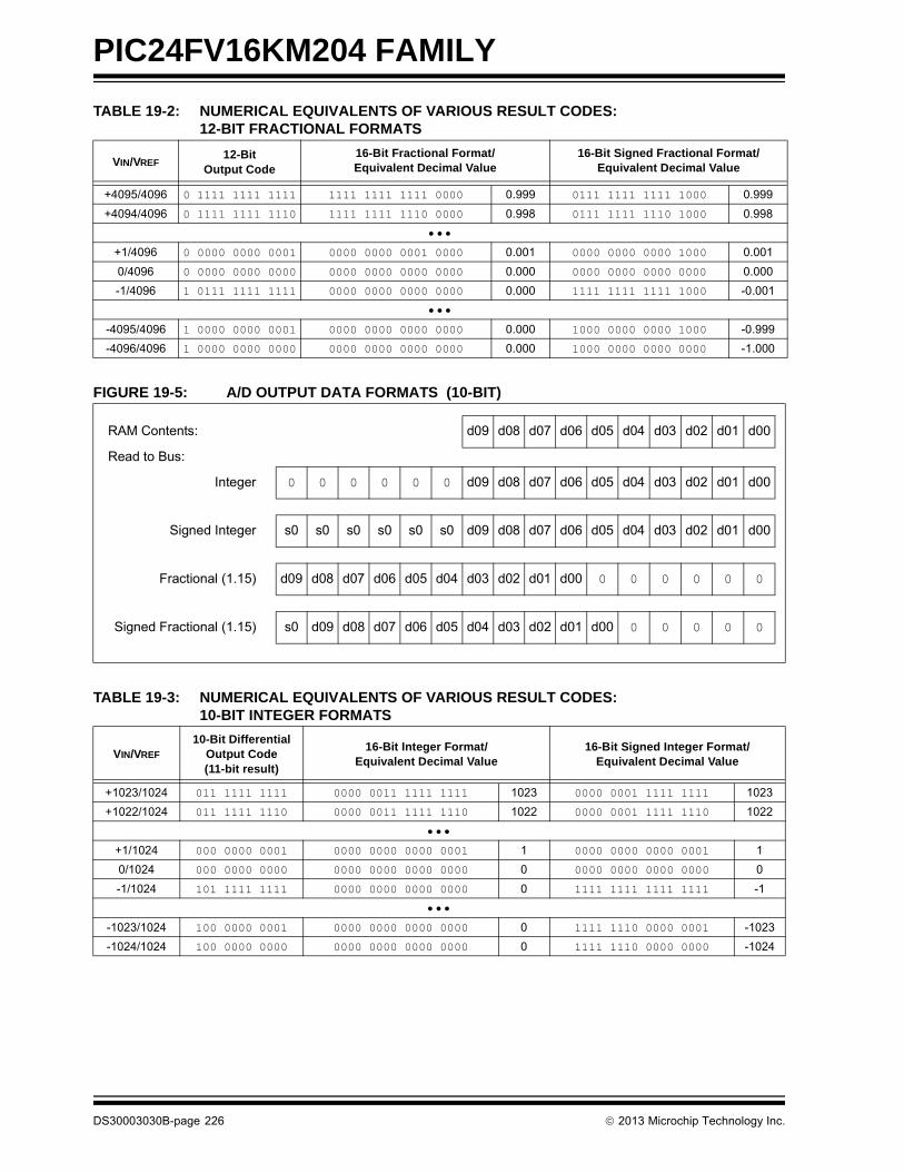
PIC24FV16KM204 FAMILY
TABLE 19-2: NUMERICAL EQUIVALENTS OF VARIOUS RESULT CODES: 12-BIT FRACTIONAL FORMATS
FIGURE 19-5: A/D OUTPUT DATA FORMATS (10-BIT)
TABLE 19-3: NUMERICAL EQUIVALENTS OF VARIOUS RESULT CODES: 10-BIT INTEGER FORMATS
VIN/VREF12-Bit
Output Code16-Bit Fractional Format/Equivalent Decimal Value
16-Bit Signed Fractional Format/Equivalent Decimal Value
+4095/4096 0 1111 1111 1111 1111 1111 1111 0000 0.999 0111 1111 1111 1000 0.999
+4094/4096 0 1111 1111 1110 1111 1111 1110 0000 0.998 0111 1111 1110 1000 0.998
+1/4096 0 0000 0000 0001 0000 0000 0001 0000 0.001 0000 0000 0000 1000 0.001
0/4096 0 0000 0000 0000 0000 0000 0000 0000 0.000 0000 0000 0000 0000 0.000
-1/4096 1 0111 1111 1111 0000 0000 0000 0000 0.000 1111 1111 1111 1000 -0.001
-4095/4096 1 0000 0000 0001 0000 0000 0000 0000 0.000 1000 0000 0000 1000 -0.999
-4096/4096 1 0000 0000 0000 0000 0000 0000 0000 0.000 1000 0000 0000 0000 -1.000
RAM Contents: d09 d08 d07 d06 d05 d04 d03 d02 d01 d00
Read to Bus:
Integer 0 0 0 0 0 0 d09 d08 d07 d06 d05 d04 d03 d02 d01 d00
Signed Integer s0 s0 s0 s0 s0 s0 d09 d08 d07 d06 d05 d04 d03 d02 d01 d00
Fractional (1.15) d09 d08 d07 d06 d05 d04 d03 d02 d01 d00 0 0 0 0 0 0
Signed Fractional (1.15) s0 d09 d08 d07 d06 d05 d04 d03 d02 d01 d00 0 0 0 0 0
VIN/VREF
10-Bit DifferentialOutput Code(11-bit result)
16-Bit Integer Format/Equivalent Decimal Value
16-Bit Signed Integer Format/Equivalent Decimal Value
+1023/1024 011 1111 1111 0000 0011 1111 1111 1023 0000 0001 1111 1111 1023
+1022/1024 011 1111 1110 0000 0011 1111 1110 1022 0000 0001 1111 1110 1022
+1/1024 000 0000 0001 0000 0000 0000 0001 1 0000 0000 0000 0001 1
0/1024 000 0000 0000 0000 0000 0000 0000 0 0000 0000 0000 0000 0
-1/1024 101 1111 1111 0000 0000 0000 0000 0 1111 1111 1111 1111 -1
-1023/1024 100 0000 0001 0000 0000 0000 0000 0 1111 1110 0000 0001 -1023
-1024/1024 100 0000 0000 0000 0000 0000 0000 0 1111 1110 0000 0000 -1024
DS30003030B-page 226 2013 Microchip Technology Inc.

PIC24FV16KM204 FAMILY
TABLE 19-4: NUMERICAL EQUIVALENTS OF VARIOUS RESULT CODES: 10-BIT FRACTIONAL FORMATS
VIN/VREF
10-Bit DifferentialOutput Code(11-bit result)
16-Bit Fractional Format/Equivalent Decimal Value
16-Bit Signed Fractional Format/Equivalent Decimal Value
+1023/1024 011 1111 1111 1111 1111 1100 0000 0.999 0111 1111 1110 0000 0.999
+1022/1024 011 1111 1110 1111 1111 1000 0000 0.998 0111 1111 1000 0000 0.998
+1/1024 000 0000 0001 0000 0000 0100 0000 0.001 0000 0000 0010 0000 0.001
0/1024 000 0000 0000 0000 0000 0000 0000 0.000 0000 0000 0000 0000 0.000
-1/1024 101 1111 1111 0000 0000 0000 0000 0.000 1111 1111 1110 0000 -0.001
-1023/1024 100 0000 0001 0000 0000 0000 0000 0.000 1000 0000 0010 0000 -0.999
-1024/1024 100 0000 0000 0000 0000 0000 0000 0.000 1000 0000 0000 0000 -1.000
2013 Microchip Technology Inc. DS30003030B-page 227

PIC24FV16KM204 FAMILY
NOTES:
DS30003030B-page 228 2013 Microchip Technology Inc.
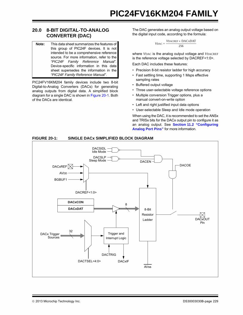
PIC24FV16KM204 FAMILY
20.0 8-BIT DIGITAL-TO-ANALOG CONVERTER (DAC)
PIC24FV16KM204 family devices include two 8-bitDigital-to-Analog Converters (DACs) for generatinganalog outputs from digital data. A simplified blockdiagram for a single DAC is shown in Figure 20-1. Bothof the DACs are identical.
The DAC generates an analog output voltage based onthe digital input code, according to the formula:
where VDAC is the analog output voltage and VDACREF
is the reference voltage selected by DACREF<1:0>.
Each DAC includes these features:
• Precision 8-bit resistor ladder for high accuracy
• Fast settling time, supporting 1 Msps effective sampling rates
• Buffered output voltage
• Three user-selectable voltage reference options
• Multiple conversion Trigger options, plus a manual convert-on-write option
• Left and right justified input data options
• User-selectable Sleep and Idle mode operation
When using the DAC, it is recommended to set the ANSxand TRISx bits for the DACx output pin to configure it asan analog output. See Section 11.2 “ConfiguringAnalog Port Pins” for more information.
FIGURE 20-1: SINGLE DACx SIMPLIFIED BLOCK DIAGRAM
Note: This data sheet summarizes the features ofthis group of PIC24F devices. It is notintended to be a comprehensive referencesource. For more information, refer to the“PIC24F Family Reference Manual”.Device-specific information in this datasheet supersedes the information in the“PIC24F Family Reference Manual”.
VDACREF DACxDAT
256VDAC =
DACxCON
Resistor
Ladder
AVss
8
DACTSEL<4:0>
Trigger and
Interrupt Logic
DACxIF
DACxREF
AVDD
BGBUF1
DACREF<1:0>
DACxOUT
DACEN
DACSIDLIdle Mode
DACSLPSleep Mode
DACTRIG
8-Bit
Pin
32DACx Trigger
Sources
DACxDAT
DACOE
2013 Microchip Technology Inc. DS30003030B-page 229

PIC24FV16KM204 FAMILY
REGISTER 20-1: DACxCON: DACx CONTROL REGISTER
R/W-0 U-0 R/W-0 R/W-0 R/W-0 U-0 R/W-0 R/W-0
DACEN — DACSIDL DACSLP DACFM — SRDIS DACTRIG
bit 15 bit 8
R/W-0 R/W-0 R/W-0 R/W-0 R/W-0 R/W-0 R/W-0 R/W-0
DACOE DACTSEL4 DACTSEL3 DACTSEL2 DACTSEL1 DACTSEL0 DACREF1 DACREF0
bit 7 bit 0
Legend:
R = Readable bit W = Writable bit U = Unimplemented bit, read as ‘0’
-n = Value at POR ‘1’ = Bit is set ‘0’ = Bit is cleared x = Bit is unknown
bit 15 DACEN: DACx Enable bit
1 = Module is enabled0 = Module is disabled
bit 14 Unimplemented: Read as ‘0’
bit 13 DACSIDL: DACx Stop in Idle Mode bit
1 = Discontinues module operation when device enters Idle mode0 = Continues module operation in Idle mode
bit 12 DACSLP: DACx Enable Peripheral During Sleep bit
1 = DACx continues to output the most recent value of DACxDAT during Sleep mode0 = DACx is powered down in Sleep mode; DACxOUT pin is controlled by the TRISx and LATx bits
bit 11 DACFM: DACx Data Format Select bit
1 = Data is left justified (data stored in DACxDAT<15:8>)0 = Data is right justified (data stored in DACxDAT<7:0>)
bit 10 Unimplemented: Read as ‘0’
bit 9 SRDIS: Soft Reset Disable bit
1 = DACxCON and DACxDAT SFRs reset only on a POR or BOR Reset0 = DACxCON and DACxDAT SFRs reset on any type of device Reset
bit 8 DACTRIG: DACx Trigger Input Enable bit
1 = Analog output value updates when the selected (by DACTSEL<4:0>) event occurs0 = Analog output value updates as soon as DACxDAT is written (DAC Trigger is ignored)
bit 7 DACOE: DACx Output Enable bit
1 = DACx output pin is enabled and driven on the DACxOUT pin0 = DACx output pin is disabled, DACx output is available internally to other peripherals only
Note 1: BGBUF1 voltage is configured by BUFREF<1:0> (BUFCON0<1:0>).
DS30003030B-page 230 2013 Microchip Technology Inc.

PIC24FV16KM204 FAMILY
bit 6-2 DACTSEL<4:0>: DACx Trigger Source Select bits
11101-11111 = Unused11100 = CTMU11011 = A/D11010 = Comparator 311001 = Comparator 211000 = Comparator 110011 to 10111 = Unused10010 = CLC2 output10001 = CLC1 output01100 to 10000 = Unused01011 = Timer1 Sync output01010 = External Interrupt 201001 = External Interrupt 101000 = External Interrupt 00011x = Unused00101 = MCCP5 or SCCP5 Sync output00100 = MCCP4 or SCCP4 Sync output00011 = MCCP3 or SCCP3 Sync output00010 = MCCP2 or SCCP2 Sync output00001 = MCCP1 or SCCP1 Sync output00000 = Unused
bit 1-0 DACREF<1:0>: DACx Reference Source Select bits
11 = Internal Band Gap Buffer 1 (BGBUF1)(1)
10 = AVDD
01 = DVREF+00 = Reference is not connected (lowest power but no DAC functionality)
REGISTER 20-1: DACxCON: DACx CONTROL REGISTER (CONTINUED)
Note 1: BGBUF1 voltage is configured by BUFREF<1:0> (BUFCON0<1:0>).
2013 Microchip Technology Inc. DS30003030B-page 231

PIC24FV16KM204 FAMILY
REGISTER 20-2: BUFCON0: INTERNAL VOLTAGE REFERENCE CONTROL REGISTER 0
U-0 U-0 U-0 U-0 U-0 U-0 U-0 U-0
— — — — — — — —
bit 15 bit 8
U-0 U-0 U-0 U-0 U-0 U-0 R/W-0 R/W-1
— — — — — — BUFREF1 BUFREF0
bit 7 bit 0
Legend:
R = Readable bit W = Writable bit U = Unimplemented bit, read as ‘0’
-n = Value at POR ‘1’ = Bit is set ‘0’ = Bit is cleared x = Bit is unknown
bit 15-2 Unimplemented: Read as ‘0’
bit 1-0 BUFREF<1:0>: Internal Voltage Reference Select bits
11 = Reference output is set at 4 * BGBUF1(1)
10 = Reference output is set at 2 * BGBUF1(2)
01 = Reference output is set at BGBUF100 = Reserved, do not use
Note 1: Available only on PIC24FV16KMXXX devices. The reference may not be within specifications for VDD below specified levels; see Table 27-15 for minimum VDD limits.
2: The reference may not be within specifications for VDD below specified levels; see Table 27-15 for minimum VDD limits.
DS30003030B-page 232 2013 Microchip Technology Inc.
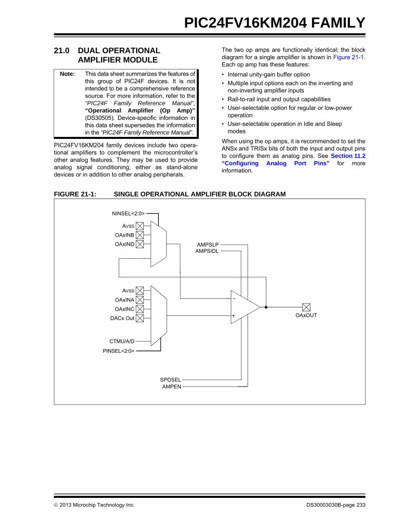
PIC24FV16KM204 FAMILY
21.0 DUAL OPERATIONAL AMPLIFIER MODULE
PIC24FV16KM204 family devices include two opera-tional amplifiers to complement the microcontroller’sother analog features. They may be used to provideanalog signal conditioning, either as stand-alonedevices or in addition to other analog peripherals.
The two op amps are functionally identical; the blockdiagram for a single amplifier is shown in Figure 21-1.Each op amp has these features:
• Internal unity-gain buffer option
• Multiple input options each on the inverting and non-inverting amplifier inputs
• Rail-to-rail input and output capabilities
• User-selectable option for regular or low-power operation
• User-selectable operation in Idle and Sleep modes
When using the op amps, it is recommended to set theANSx and TRISx bits of both the input and output pinsto configure them as analog pins. See Section 11.2“Configuring Analog Port Pins” for moreinformation.
FIGURE 21-1: SINGLE OPERATIONAL AMPLIFIER BLOCK DIAGRAM
Note: This data sheet summarizes the features ofthis group of PIC24F devices. It is notintended to be a comprehensive referencesource. For more information, refer to the“PIC24F Family Reference Manual”,“Operational Amplifier (Op Amp)”(DS30505). Device-specific information inthis data sheet supersedes the informationin the “PIC24F Family Reference Manual”.
SPDSEL
+
–
AMPEN
OAxOUT
AMPSIDLAMPSLP
NINSEL<2:0>
PINSEL<2:0>
OAxINB
OAxIND
AVSS
CTMU/A/D
OAxINA
OAxINC
DACx Out
AVSS
2013 Microchip Technology Inc. DS30003030B-page 233

PIC24FV16KM204 FAMILY
REGISTER 21-1: AMPxCON: OP AMP x CONTROL REGISTER(1)
R/W-0 U-0 R/W-0 R/W-0 U-0 U-0 U-0 U-0
AMPEN — AMPSIDL AMPSLP — — — —
bit 15 bit 8
R/W-0 U-0 R/W-0 R/W-0 R/W-0 R/W-0 R/W-0 R/W-0
SPDSEL — NINSEL2 NINSEL1 NINSEL0 PINSEL2 PINSEL1 PINSEL0
bit 7 bit 0
Legend:
R = Readable bit W = Writable bit U = Unimplemented bit, read as ‘0’
-n = Value at POR ‘1’ = Bit is set ‘0’ = Bit is cleared x = Bit is unknown
bit 15 AMPEN: Op Amp x Control Module Enable bit
1 = Module is enabled0 = Module is disabled
bit 14 Unimplemented: Read as ‘0’
bit 13 AMPSIDL: Op Amp x Peripheral Stop in Idle Mode bit
1 = Discontinues module operation when device enters Idle mode0 = Continues module operation in Idle mode
bit 12 AMPSLP: Op Amp x Peripheral Enabled in Sleep Mode bit
1 = Continues module operation when device enters Sleep mode0 = Discontinues module operation in Sleep mode
bit 11-8 Unimplemented: Read as ‘0’
bit 7 SPDSEL: Op Amp x Power/Speed Select bit
1 = Higher power and bandwidth (faster response time)0 = Lower power and bandwidth (slower response time)
bit 6 Unimplemented: Read as ‘0’
bit 5-3 NINSEL<2:0>: Negative Op Amp Input Select bits
111 = Reserved; do not use110 = Reserved; do not use101 = Op amp negative input is connected to the op amp output (voltage follower)100 = Reserved; do not use011 = Reserved; do not use010 = Op amp negative input is connected to the OAxIND pin001 = Op amp negative input is connected to the OAxINB pin000 = Op amp negative input is connected to AVSS
bit 2-0 PINSEL<2:0>: Positive Op Amp Input Select bits
111 = Op amp positive input is connected to the output of the A/D input multiplexer110 = Reserved; do not use101 = Op amp positive input is connected to the DAC1 output for OA1 (DAC2 output for OA2)100 = Reserved; do not use011 = Reserved; do not use010 = Op amp positive input is connected to the OAxINC pin001 = Op amp positive input is connected to the OAxINA pin000 = Op amp positive input is connected to AVSS
Note 1: This register is available only on PIC24F(V)16KM2XX devices.
DS30003030B-page 234 2013 Microchip Technology Inc.

PIC24FV16KM204 FAMILY
22.0 COMPARATOR MODULE
The comparator module provides three dual inputcomparators. The inputs to the comparator can beconfigured to use any one of four external analoginputs, as well as a voltage reference input from eitherthe Internal Band Gap Buffer 1 (BGBUF1) or the com-parator voltage reference generator.
The comparator outputs may be directly connected tothe CxOUT pins. When the respective COE bit equals‘1’, the I/O pad logic makes the unsynchronized outputof the comparator available on the pin.
A simplified block diagram of the module is shown inFigure 22-1. Diagrams of the possible individualcomparator configurations are shown in Figure 22-2.
Each comparator has its own control register,CMxCON (Register 22-1), for enabling and configuringits operation. The output and event status of all threecomparators is provided in the CMSTAT register(Register 22-2).
FIGURE 22-1: COMPARATOR x MODULE BLOCK DIAGRAM
Note: This data sheet summarizes the featuresof this group of PIC24F devices. It is notintended to be a comprehensive refer-ence source. For more information on theComparator module, refer to the “PIC24FFamily Reference Manual”, “ScalableComparator Module” (DS39734).
C1
VIN-
VIN+
CXINB
CXINC
CXINA
CXIND
CVREF
BGBUF1
C3
VIN-
VIN+
COE
C1OUTPin
CPOL
CEVT
EVPOL<1:0>
COUT
InputSelectLogic
CCH<1:0>CREF<1:0>
COE
C3OUTPin
CPOL
CEVT
EVPOL<1:0>
COUT
C2
VIN-
VIN+
COE
C2OUTPin
CPOL
CEVT
COUT
Trigger/InterruptLogic
Trigger/InterruptLogic
EVPOL<1:0>
Trigger/InterruptLogic
2013 Microchip Technology Inc. DS30003030B-page 235

PIC24FV16KM204 FAMILY
FIGURE 22-2: INDIVIDUAL COMPARATOR CONFIGURATIONS
Cx
VIN-
VIN+Off (Read as ‘0’)
Comparator OffCON = 0, CREF<1:0> = xx, CCH<1:0> = xx
Comparator CxINB > CxINA Compare CON = 1, CREF<1:0> = 00, CCH<1:0> = 00
COE
CxOUT
Cx
VIN-
VIN+
COE
CXINB
CXINA
Comparator CxIND > CxINA Compare CON = 1, CREF<1:0> = 00, CCH<1:0> = 10
Cx
VIN-
VIN+
COE
CxOUT
CXIND
CXINA
Comparator CxINC > CxINA Compare CON = 1, CREF<1:0> = 00, CCH<1:0> = 01
Cx
VIN-
VIN+
COE
CXINC
CXINA
Comparator BGBUF1 > CxINA Compare CON = 1, CREF<1:0> = 00, CCH<1:0> = 11
Cx
VIN-
VIN+
COE
BGBUF1
CXINA
Comparator CxINB > CVREF Compare CON = 1, CREF<1:0> = 01, CCH<1:0> = 00
Cx
VIN-
VIN+
COE
CXINB
CVREF
Comparator CxIND > DAC1OUT Compare CON = 1, CREF<1:0> = 10, CCH<1:0> = 10
Cx
VIN-
VIN+
COE
CXIND
DAC1OUT
Comparator CxINC > CVREF Compare CON = 1, CREF<1:0> = 01, CCH<1:0> = 01
Cx
VIN-
VIN+
COE
CXINC
CVREF
Comparator BGBUF1 > DAC2OUT Compare CON = 1, CREF<1:0> = 11, CCH<1:0> = 11
Cx
VIN-
VIN+
COEBGBUF1
DAC2OUT
Pin
Pin
CxOUTPin
CxOUTPin
CxOUTPin
CxOUTPin
CxOUTPin
CxOUTPin
CxOUTPin
–
–
–
–
– –
–
–
–
DS30003030B-page 236 2013 Microchip Technology Inc.

PIC24FV16KM204 FAMILY
REGISTER 22-1: CMxCON: COMPARATOR x CONTROL REGISTERS
R/W-0 R/W-0 R/W-0 R/W-0 U-0 U-0 R/W-0 R-0
CON COE CPOL CLPWR — — CEVT COUT
bit 15 bit 8
R/W-0 R/W-0 U-0 R/W-0 R/W-0 U-0 R/W-0 R/W-0
EVPOL1(2) EVPOL0(2) — CREF1 CREF0 — CCH1 CCH0
bit 7 bit 0
Legend:
R = Readable bit W = Writable bit U = Unimplemented bit, read as ‘0’
-n = Value at POR ‘1’ = Bit is set ‘0’ = Bit is cleared x = Bit is unknown
bit 15 CON: Comparator x Enable bit
1 = Comparator is enabled0 = Comparator is disabled
bit 14 COE: Comparator x Output Enable bit
1 = Comparator output is present on the CxOUT pin0 = Comparator output is internal only
bit 13 CPOL: Comparator x Output Polarity Select bit
1 = Comparator output is inverted0 = Comparator output is not inverted
bit 12 CLPWR: Comparator x Low-Power Mode Select bit
1 = Comparator operates in Low-Power mode0 = Comparator does not operate in Low-Power mode
bit 11-10 Unimplemented: Read as ‘0’
bit 9 CEVT: Comparator x Event bit
1 = Comparator event, defined by EVPOL<1:0>, has occurred; subsequent Triggers and interrupts aredisabled until the bit is cleared
0 = Comparator event has not occurred
bit 8 COUT: Comparator x Output bit
When CPOL = 0:1 = VIN+ > VIN-0 = VIN+ < VIN-
When CPOL = 1:1 = VIN+ < VIN-0 = VIN+ > VIN-
bit 7-6 EVPOL<1:0>: Trigger/Event/Interrupt Polarity Select bits(2)
11 = Trigger/event/interrupt is generated on any change of the comparator output (while CEVT = 0)10 = Trigger/event/interrupt is generated on the high-to-low transition of the comparator output01 = Trigger/event/interrupt is generated on the low-to-high transition of the comparator output00 = Trigger/event/interrupt generation is disabled
bit 5 Unimplemented: Read as ‘0’
bit 4-3 CREF<1:0>: Comparator x Reference Select bits (non-inverting input)
11 = Non-inverting input connects to the DAC2 output10 = Non-inverting input connects to the DAC1 output01 = Non-inverting input connects to the internal CVREF voltage00 = Non-inverting input connects to the CxINA pin
Note 1: BGBUF1 voltage is configured by BUFREF1<1:0> (BUFCON0<1:0>).
2: If the EVPOL<1:0> bits are set to a value other than ‘00’, the first interrupt generated will occur on any transition of COUT. Subsequent interrupts will occur based on the EVPOLx bits setting.
2013 Microchip Technology Inc. DS30003030B-page 237

PIC24FV16KM204 FAMILY
bit 2 Unimplemented: Read as ‘0’
bit 1-0 CCH<1:0>: Comparator x Channel Select bits
11 = Inverting input of the comparator connects to BGBUF1(1)
10 = Inverting input of the comparator connects to the CxIND pin01 = Inverting input of the comparator connects to the CxINC pin00 = Inverting input of the comparator connects to the CxINB pin
REGISTER 22-1: CMxCON: COMPARATOR x CONTROL REGISTERS (CONTINUED)
Note 1: BGBUF1 voltage is configured by BUFREF1<1:0> (BUFCON0<1:0>).
2: If the EVPOL<1:0> bits are set to a value other than ‘00’, the first interrupt generated will occur on any transition of COUT. Subsequent interrupts will occur based on the EVPOLx bits setting.
REGISTER 22-2: CMSTAT: COMPARATOR MODULE STATUS REGISTER
R/W-0 U-0 U-0 U-0 U-0 R-0, HSC R-0, HSC R-0, HSC
CMIDL — — — — C3EVT(1) C2EVT(1) C1EVT
bit 15 bit 8
U-0 U-0 U-0 U-0 U-0 R-0, HSC R-0, HSC R-0, HSC
— — — — — C3OUT(1) C2OUT(1) C1OUT
bit 7 bit 0
Legend: HSC = Hardware Settable/Clearable bit
R = Readable bit W = Writable bit U = Unimplemented bit, read as ‘0’
-n = Value at POR ‘1’ = Bit is set ‘0’ = Bit is cleared x = Bit is unknown
bit 15 CMIDL: Comparator x Stop in Idle Mode bit
1 = Comparator interrupts are disabled in Idle mode; enabled comparators remain operational0 = Continues operation of all enabled comparators in Idle mode
bit 14-11 Unimplemented: Read as ‘0’
bit 10 C3EVT: Comparator 3 Event Status bit (read-only)(1)
Shows the current event status of Comparator 3 (CM3CON<9>).
bit 9 C2EVT: Comparator 2 Event Status bit (read-only)(1)
Shows the current event status of Comparator 2 (CM2CON<9>).
bit 8 C1EVT: Comparator 1 Event Status bit (read-only)
Shows the current event status of Comparator 1 (CM1CON<9>).
bit 7-3 Unimplemented: Read as ‘0’
bit 2 C3OUT: Comparator 3 Output Status bit (read-only)(1)
Shows the current output of Comparator 3 (CM3CON<8>).
bit 1 C2OUT: Comparator 2 Output Status bit (read-only)(1)
Shows the current output of Comparator 2 (CM2CON<8>).
bit 0 C1OUT: Comparator 1 Output Status bit (read-only)
Shows the current output of Comparator 1 (CM1CON<8>).
Note 1: Comparator 2 and Comparator 3 are only available on PIC24F(V)16KM2XX devices.
DS30003030B-page 238 2013 Microchip Technology Inc.

PIC24FV16KM204 FAMILY
23.0 COMPARATOR VOLTAGE REFERENCE
23.1 Configuring the Comparator Voltage Reference
The comparator voltage reference module is controlledthrough the CVRCON register (Register 23-1). Thecomparator voltage reference provides a range ofoutput voltages with 32 distinct levels.
The comparator voltage reference supply voltage cancome from either VDD and VSS, or the external VREF+and VREF-. The voltage source is selected by theCVRSS bit (CVRCON<5>).
The settling time of the comparator voltage referencemust be considered when changing the CVREF output.
FIGURE 23-1: COMPARATOR VOLTAGE REFERENCE BLOCK DIAGRAM
Note: This data sheet summarizes the features ofthis group of PIC24F devices. It is notintended to be a comprehensive referencesource. For more information on theComparator Voltage Reference, refer tothe “PIC24F Family Reference Manual”,“Comparator Voltage ReferenceModule” (DS39709).
32-t
o-1
MU
X
CVR<3:0>
RCVREN
CVRSS = 0AVDD
VREF+CVRSS = 1
CVRSS = 0
VREF-CVRSS = 1
R
R
R
R
R
R
32 StepsCVREF
AVSS
2013 Microchip Technology Inc. DS30003030B-page 239
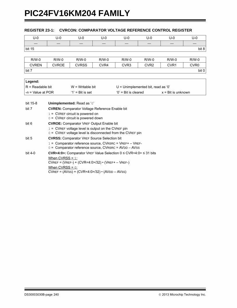
PIC24FV16KM204 FAMILY
REGISTER 23-1: CVRCON: COMPARATOR VOLTAGE REFERENCE CONTROL REGISTER
U-0 U-0 U-0 U-0 U-0 U-0 U-0 U-0
— — — — — — — —
bit 15 bit 8
R/W-0 R/W-0 R/W-0 R/W-0 R/W-0 R/W-0 R/W-0 R/W-0
CVREN CVROE CVRSS CVR4 CVR3 CVR2 CVR1 CVR0
bit 7 bit 0
Legend:
R = Readable bit W = Writable bit U = Unimplemented bit, read as ‘0’
-n = Value at POR ‘1’ = Bit is set ‘0’ = Bit is cleared x = Bit is unknown
bit 15-8 Unimplemented: Read as ‘0’
bit 7 CVREN: Comparator Voltage Reference Enable bit
1 = CVREF circuit is powered on0 = CVREF circuit is powered down
bit 6 CVROE: Comparator VREF Output Enable bit
1 = CVREF voltage level is output on the CVREF pin0 = CVREF voltage level is disconnected from the CVREF pin
bit 5 CVRSS: Comparator VREF Source Selection bit
1 = Comparator reference source, CVRSRC = VREF+ – VREF-0 = Comparator reference source, CVRSRC = AVDD – AVSS
bit 4-0 CVR<4:0>: Comparator VREF Value Selection 0 ≤ CVR<4:0> ≤ 31 bits
When CVRSS = 1:CVREF = (VREF-) + (CVR<4:0>/32) • (VREF+ – VREF-)
When CVRSS = 0:CVREF = (AVSS) + (CVR<4:0>/32) • (AVDD – AVSS)
DS30003030B-page 240 2013 Microchip Technology Inc.

PIC24FV16KM204 FAMILY
24.0 CHARGE TIME MEASUREMENT UNIT (CTMU)
The Charge Time Measurement Unit (CTMU) is aflexible analog module that provides chargemeasurement, accurate differential time measurementbetween pulse sources and asynchronous pulsegeneration. Its key features include:
• Thirteen external edge input Trigger sources• Polarity control for each edge source• Control of edge sequence• Control of response to edge levels or edge
transitions• Time measurement resolution of one nanosecond• Accurate current source suitable for capacitive
measurement
Together with other on-chip analog modules, the CTMUcan be used to precisely measure time, measurecapacitance, measure relative changes in capacitanceor generate output pulses that are independent of thesystem clock. The CTMU module is ideal for interfacingwith capacitive-based touch sensors.
The CTMU is controlled through three registers:CTMUCON1, CTMUCON2 and CTMUICON.CTMUCON1 enables the module and controls the modeof operation of the CTMU, as well as controlling edgesequencing. CTMUCON2 controls edge source selec-tion and edge source polarity selection. The CTMUICONregister selects the current range of current source andtrims the current.
24.1 Measuring Capacitance
The CTMU module measures capacitance bygenerating an output pulse, with a width equal to thetime between edge events, on two separate inputchannels. The pulse edge events to both inputchannels can be selected from several internalperipheral modules (OC1, Timer1, any input capture orcomparator module) and up to 13 external pins(CTED1 through CTED13). This pulse is used with themodule’s precision current source to calculatecapacitance according to the relationship:
EQUATION 24-1:
For capacitance measurements, the A/D Convertersamples an External Capacitor (CAPP) on one of itsinput channels after the CTMU output’s pulse. A Preci-sion Resistor (RPR) provides current source calibrationon a second A/D channel. After the pulse ends, theconverter determines the voltage on the capacitor. Theactual calculation of capacitance is performed insoftware by the application.
Figure 24-1 illustrates the external connections usedfor capacitance measurements, and how the CTMUand A/D modules are related in this application. Thisexample also shows the edge events coming fromTimer1, but other configurations using external edgesources are possible. A detailed discussion on measur-ing capacitance and time with the CTMU module isprovided in the “PIC24F Family Reference Manual”.
Note: This data sheet summarizes the features ofthis group of PIC24F devices. It is notintended to be a comprehensive referencesource. For more information on theCharge Time Measurement Unit, refer tothe “PIC24F Family Reference Manual”,“Charge Time Measurement Unit(CTMU) with Threshold Detect”(DS39743).
I CdVdT-------=
2013 Microchip Technology Inc. DS30003030B-page 241

PIC24FV16KM204 FAMILY
FIGURE 24-1: TYPICAL CONNECTIONS AND INTERNAL CONFIGURATION FOR CAPACITANCE MEASUREMENT
24.2 Measuring Time
Time measurements on the pulse width can be similarlyperformed using the A/D module’s Internal Capacitor(CAD) and a precision resistor for current calibration.Figure 24-2 displays the external connections used for
time measurements, and how the CTMU and A/Dmodules are related in this application. This examplealso shows both edge events coming from the externalCTEDx pins, but other configurations using internaledge sources are possible.
FIGURE 24-2: TYPICAL CONNECTIONS AND INTERNAL CONFIGURATION FOR TIME MEASUREMENT
PIC24F Device
A/D Converter
CTMU
ANx
CAPP
Output Pulse
EDG1STAT
EDG2STAT
RPR
ANy
Timer1
Current Source
PIC24F Device
A/D Converter
CTMUCTEDX
CTEDX
ANx
Output Pulse
EDG1STAT
EDG2STAT
CAD
RPR
Current Source
DS30003030B-page 242 2013 Microchip Technology Inc.

PIC24FV16KM204 FAMILY
24.3 Pulse Generation and Delay
The CTMU module can also generate an output pulsewith edges that are not synchronous with the device’ssystem clock. More specifically, it can generate a pulsewith a programmable delay from an edge event input tothe module.
When the module is configured for pulse generationdelay by setting the TGEN bit (CTMUCON1L<12>), theinternal current source is connected to the B input ofComparator 2. A Capacitor (CDELAY) is connected tothe Comparator 2 pin, C2INB, and the ComparatorVoltage Reference, CVREF, is connected to C2INA.CVREF is then configured for a specific trip point. Themodule begins to charge CDELAY when an edge eventis detected. While CVREF is greater than the voltage onCDELAY, the CTPLS pin is high.
When the voltage on CDELAY equals CVREF, CTPLSgoes low. With Comparator 2 configured as the secondedge, this stops the CTMU from charging. In this stateevent, the CTMU automatically connects to ground.The IDISSEN bit doesn’t need to be set and clearedbefore the next CTPLS cycle.
Figure 24-3 illustrates the external connections forpulse generation, as well as the relationship of thedifferent analog modules required. While CTED1 isshown as the input pulse source, other options areavailable. A detailed discussion on pulse generationwith the CTMU module is provided in the “PIC24FFamily Reference Manual”.
FIGURE 24-3: TYPICAL CONNECTIONS AND INTERNAL CONFIGURATION FOR PULSE DELAY GENERATION
C2
CVREF
CTPLS
PIC24F Device
Current
Comparator
CTMU
CTED1
C2INB
CDELAY
EDG1STAT
–
Q
QD
CK
EDG2STAT
Source
R
VDDEDG1STAT EDG2STAT
2013 Microchip Technology Inc. DS30003030B-page 243

PIC24FV16KM204 FAMILY
REGISTER 24-1: CTMUCON1L: CTMU CONTROL 1 LOW REGISTER
R/W-0 U-0 R/W-0 R/W-0 R/W-0 R/W-0 R/W-0 R/W-0
CTMUEN — CTMUSIDL TGEN EDGEN EDGSEQEN IDISSEN CTTRIG
bit 15 bit 8
R/W-0 R/W-0 R/W-0 R/W-0 R/W-0 R/W-0 R/W-0 R/W-0
ITRIM5 ITRIM4 ITRIM3 ITRIM2 ITRIM1 ITRIM0 IRNG1 IRNG0
bit 7 bit 0
Legend:
R = Readable bit W = Writable bit U = Unimplemented bit, read as ‘0’
-n = Value at POR ‘1’ = Bit is set ‘0’ = Bit is cleared x = Bit is unknown
bit 15 CTMUEN: CTMU Enable bit
1 = Module is enabled0 = Module is disabled
bit 14 Unimplemented: Read as ‘0’
bit 13 CTMUSIDL: CTMU Stop in Idle Mode bit
1 = Discontinues module operation when device enters Idle mode0 = Continues module operation in Idle mode
bit 12 TGEN: Time Generation Enable bit
1 = Enables edge delay generation0 = Disables edge delay generation
bit 11 EDGEN: Edge Enable bit
1 = Edges are not blocked0 = Edges are blocked
bit 10 EDGSEQEN: Edge Sequence Enable bit
1 = Edge 1 event must occur before Edge 2 event can occur0 = No edge sequence is needed
bit 9 IDISSEN: Analog Current Source Control bit
1 = Analog current source output is grounded0 = Analog current source output is not grounded
bit 8 CTTRIG: CTMU Trigger Control bit
1 = Trigger output is enabled0 = Trigger output is disabled
bit 7-2 ITRIM<5:0>: Current Source Trim bits
011111 = Maximum positive change from nominal current011110 •••000001 = Minimum positive change from nominal current000000 = Nominal current output specified by IRNG<1:0>111111 = Minimum negative change from nominal current•••100010 100001 = Maximum negative change from nominal current
DS30003030B-page 244 2013 Microchip Technology Inc.
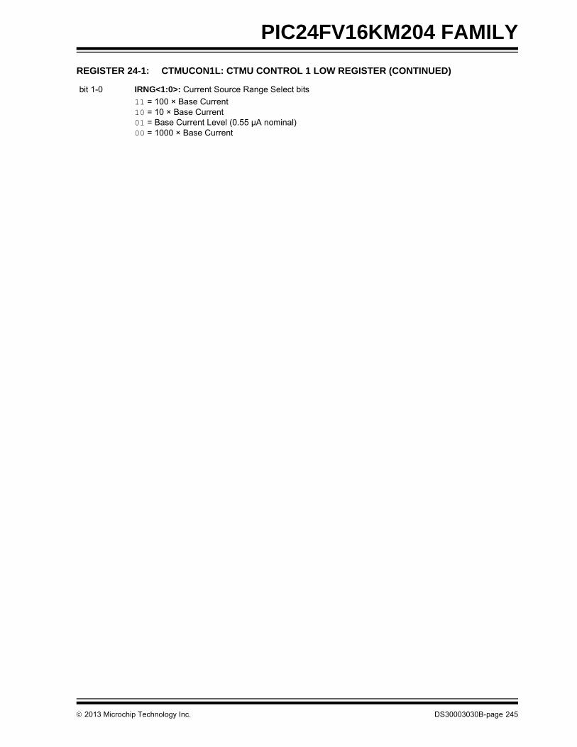
PIC24FV16KM204 FAMILY
bit 1-0 IRNG<1:0>: Current Source Range Select bits
11 = 100 × Base Current10 = 10 × Base Current01 = Base Current Level (0.55 µA nominal)00 = 1000 × Base Current
REGISTER 24-1: CTMUCON1L: CTMU CONTROL 1 LOW REGISTER (CONTINUED)
2013 Microchip Technology Inc. DS30003030B-page 245

PIC24FV16KM204 FAMILY
REGISTER 24-2: CTMUCON1H: CTMU CONTROL 1 HIGH REGISTER
R/W-0 R/W-0 R/W-0 R/W-0 R/W-0 R/W-0 R/W-0 R/W-0
EDG1MOD EDG1POL EDG1SEL3 EDG1SEL2 EDG1SEL1 EDG1SEL0 EDG2STAT EDG1STAT
bit 15 bit 8
R/W-0 R/W-0 R/W-0 R/W-0 R/W-0 R/W-0 U-0 U-0
EDG2MOD EDG2POL EDG2SEL3 EDG2SEL2 EDG2SEL1 EDG2SEL0 — —
bit 7 bit 0
Legend:
R = Readable bit W = Writable bit U = Unimplemented bit, read as ‘0’
-n = Value at POR ‘1’ = Bit is set ‘0’ = Bit is cleared x = Bit is unknown
bit 15 EDG1MOD: Edge 1 Edge-Sensitive Select bit
1 = Input is edge-sensitive0 = Input is level-sensitive
bit 14 EDG1POL: Edge 1 Polarity Select bit
1 = Edge 1 is programmed for a positive edge response0 = Edge 1 is programmed for a negative edge response
bit 13-10 EDG1SEL<3:0>: Edge 1 Source Select bits
1111 = Edge 1 source is the Comparator 3 output1110 = Edge 1 source is the Comparator 2 output1101 = Edge 1 source is the Comparator 1 output1100 = Edge 1 source is CLC21011 = Edge 1 source is CLC11010 = Edge 1 source is the MCCP2 Compare Event (CCP2IF)1001 = Edge 1 source is CTED8(1)
1000 = Edge 1 source is CTED7(1)
0111 = Edge 1 source is CTED60110 = Edge 1 source is CTED50101 = Edge 1 source is CTED40100 = Edge 1 source is CTED3(2)
0011 = Edge 1 source is CTED10010 = Edge 1 source is CTED20001 = Edge 1 source is the MCCP1 Compare Event (CCP1IF)0000 = Edge 1 source is Timer1
bit 9 EDG2STAT: Edge 2 Status bit
Indicates the status of Edge 2 and can be written to control the current source.1 = Edge 2 has occurred0 = Edge 2 has not occurred
bit 8 EDG1STAT: Edge 1 Status bit
Indicates the status of Edge 1 and can be written to control the current source.1 = Edge 1 has occurred0 = Edge 1 has not occurred
bit 7 EDG2MOD: Edge 2 Edge-Sensitive Select bit
1 = Input is edge-sensitive0 = Input is level-sensitive
Note 1: Edge sources, CTED7 and CTED8, are not available on 28-pin and 20-pin devices.
2: Edge sources, CTED3, CTED9 and CTED11, are not available on 20-pin devices.
DS30003030B-page 246 2013 Microchip Technology Inc.

PIC24FV16KM204 FAMILY
bit 6 EDG2POL: Edge 2 Polarity Select bit
1 = Edge 2 is programmed for a positive edge0 = Edge 2 is programmed for a negative edge
bit 5-2 EDG2SEL<3:0>: Edge 2 Source Select bits
1111 = Edge 2 source is the Comparator 3 output1110 = Edge 2 source is the Comparator 2 output1101 = Edge 2 source is the Comparator 1 output1100 = Unimplemented; do not use1011 = Edge 2 source is CLC11010 = Edge 2 source is the MCCP2 Compare Event (CCP2IF)1001 = Unimplemented; do not use1000 = Edge 2 source is CTED130111 = Edge 2 source is CTED120110 = Edge 2 source is CTED11(2)
0101 = Edge 2 source is CTED100100 = Edge 2 source is CTED9(2)
0011 = Edge 2 source is CTED10010 = Edge 2 source is CTED20001 = Edge 2 source is the MCCP1 Compare Event (CCP1IF)0000 = Edge 2 source is Timer1
bit 1-0 Unimplemented: Read as ‘0’
REGISTER 24-2: CTMUCON1H: CTMU CONTROL 1 HIGH REGISTER (CONTINUED)
Note 1: Edge sources, CTED7 and CTED8, are not available on 28-pin and 20-pin devices.
2: Edge sources, CTED3, CTED9 and CTED11, are not available on 20-pin devices.
2013 Microchip Technology Inc. DS30003030B-page 247
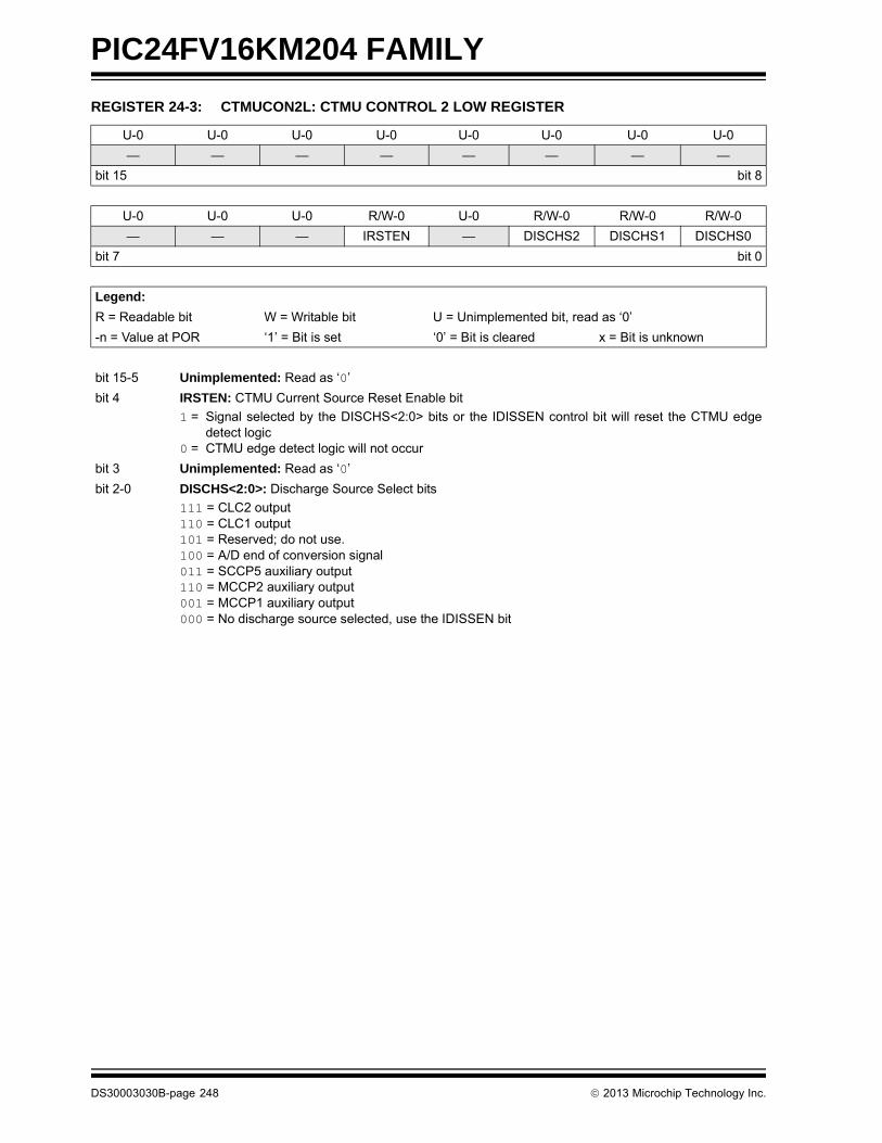
PIC24FV16KM204 FAMILY
REGISTER 24-3: CTMUCON2L: CTMU CONTROL 2 LOW REGISTERU-0 U-0 U-0 U-0 U-0 U-0 U-0 U-0
— — — — — — — —
bit 15 bit 8
U-0 U-0 U-0 R/W-0 U-0 R/W-0 R/W-0 R/W-0
— — — IRSTEN — DISCHS2 DISCHS1 DISCHS0
bit 7 bit 0
Legend:
R = Readable bit W = Writable bit U = Unimplemented bit, read as ‘0’
-n = Value at POR ‘1’ = Bit is set ‘0’ = Bit is cleared x = Bit is unknown
bit 15-5 Unimplemented: Read as ‘0’
bit 4 IRSTEN: CTMU Current Source Reset Enable bit
1 = Signal selected by the DISCHS<2:0> bits or the IDISSEN control bit will reset the CTMU edgedetect logic
0 = CTMU edge detect logic will not occur
bit 3 Unimplemented: Read as ‘0’
bit 2-0 DISCHS<2:0>: Discharge Source Select bits
111 = CLC2 output110 = CLC1 output101 = Reserved; do not use.100 = A/D end of conversion signal011 = SCCP5 auxiliary output110 = MCCP2 auxiliary output001 = MCCP1 auxiliary output000 = No discharge source selected, use the IDISSEN bit
DS30003030B-page 248 2013 Microchip Technology Inc.

PIC24FV16KM204 FAMILY
25.0 SPECIAL FEATURES
PIC24FXXXXX family devices include several featuresintended to maximize application flexibility and reli-ability, and minimize cost through elimination ofexternal components. These are:
• Flexible Configuration• Watchdog Timer (WDT)• Code Protection• In-Circuit Serial Programming™ (ICSP™)• In-Circuit Emulation
25.1 Configuration Bits
The Configuration bits can be programmed (read as‘0’) or left unprogrammed (read as ‘1’) to select variousdevice configurations. These bits are mapped, startingat program memory location, F80000h. A complete listof Configuration register locations is provided inTable 25-1. A detailed explanation of the various bitfunctions is provided in Register 25-1 throughRegister 25-9.
The address, F80000h, is beyond the user programmemory space. In fact, it belongs to the configurationmemory space (800000h-FFFFFFh), which can only beaccessed using Table Reads and Table Writes.
TABLE 25-1: CONFIGURATION REGISTERS LOCATIONS
REGISTER 25-1: FBS: BOOT SEGMENT CONFIGURATION REGISTER
Note: This data sheet summarizes the features ofthis group of PIC24F devices. It is notintended to be a comprehensive referencesource. For more information on theWatchdog Timer, High-Level DeviceIntegration and Programming Diagnostics,refer to the individual sections of the“PIC24F Family Reference Manual”provided below:
• “Watchdog Timer (WDT)” (DS39697)• “Programming and Diagnostics”
(DS39716)
Configuration Register
Address
FBS F80000
FGS F80004
FOSCSEL F80006
FOSC F80008
FWDT F8000A
FPOR F8000C
FICD F8000E
U-0 U-0 U-0 U-0 R/W-1 R/W-1 R/W-1 R/W-1
— — — — BSS2 BSS1 BSS0 BWRP
bit 7 bit 0
Legend:
R = Readable bit W = Writable bit U = Unimplemented bit, read as ‘0’
-n = Value at POR ‘1’ = Bit is set ‘0’ = Bit is cleared x = Bit is unknown
bit 7-4 Unimplemented: Read as ‘0’
bit 3-1 BSS<2:0>: Boot Segment Program Flash Code Protection bits
111 = No boot program Flash segment011 = Reserved110 = Standard security, boot program Flash segment starts at 200h, ends at 000AFEh010 = High-security, boot program Flash segment starts at 200h, ends at 000AFEh101 = Standard security, boot program Flash segment starts at 200h, ends at 0015FEh(1)
001 = High-security, boot program Flash segment starts at 200h, ends at 0015FEh(1)
100 = Reserved000 = Reserved
bit 0 BWRP: Boot Segment Program Flash Write Protection bit
1 = Boot Segment may be written0 = Boot Segment is write-protected
Note 1: This selection should not be used in PIC24FV08KMXXX devices.
2013 Microchip Technology Inc. DS30003030B-page 249

PIC24FV16KM204 FAMILY
REGISTER 25-2: FGS: GENERAL SEGMENT CONFIGURATION REGISTER
REGISTER 25-3: FOSCSEL: OSCILLATOR SELECTION CONFIGURATION REGISTER
U-0 U-0 U-0 U-0 U-0 U-0 R/C-1 R/C-1
— — — — — — GCP GWRP
bit 7 bit 0
Legend:
R = Readable bit C = Clearable bit U = Unimplemented bit, read as ‘0’
-n = Value at POR ‘1’ = Bit is set ‘0’ = Bit is cleared x = Bit is unknown
bit 7-2 Unimplemented: Read as ‘0’
bit 1 GCP: General Segment Code Flash Code Protection bit
1 = No protection0 = Standard security is enabled
bit 0 GWRP: General Segment Code Flash Write Protection bit
1 = General Segment may be written0 = General Segment is write-protected
R/P-1 R/P-1 R/P-1 U-0 U-0 R/P-1 R/P-1 R/P-1
IESO LPRCSEL SOSCSRC — — FNOSC2 FNOSC1 FNOSC0
bit 7 bit 0
Legend:
R = Readable bit P = Programmable bit U = Unimplemented bit, read as ‘0’
-n = Value at POR ‘1’ = Bit is set ‘0’ = Bit is cleared x = Bit is unknown
bit 7 IESO: Internal External Switchover bit
1 = Internal External Switchover mode is enabled (Two-Speed Start-up is enabled)0 = Internal External Switchover mode is disabled (Two-Speed Start-up is disabled)
bit 6 LPRCSEL: Internal LPRC Oscillator Power Select bit
1 = High-Power/High-Accuracy mode0 = Low-Power/Low-Accuracy mode
bit 5 SOSCSRC: Secondary Oscillator Clock Source Configuration bit
1 = SOSC analog crystal function is available on the SOSCI/SOSCO pins0 = SOSC crystal is disabled; digital SCLKI function is selected on the SOSCO pin
bit 4-3 Unimplemented: Read as ‘0’
bit 2-0 FNOSC<2:0>: Oscillator Selection bits
000 = Fast RC Oscillator (FRC)001 = Fast RC Oscillator with Divide-by-N with PLL module (FRCDIV+PLL)010 = Primary Oscillator (XT, HS, EC)011 = Primary Oscillator with PLL module (HS+PLL, EC+PLL)100 = Secondary Oscillator (SOSC)101 = Low-Power RC Oscillator (LPRC)110 = 500 kHz Low-Power FRC Oscillator with Divide-by-N (LPFRCDIV)111 = 8 MHz FRC Oscillator with Divide-by-N (FRCDIV)
DS30003030B-page 250 2013 Microchip Technology Inc.

PIC24FV16KM204 FAMILY
REGISTER 25-4: FOSC: OSCILLATOR CONFIGURATION REGISTER
R/P-1 R/P-1 R/P-1 R/P-1 R/P-1 R/P-1 R/P-1 R/P-1
FCKSM1 FCKSM0 SOSCSEL POSCFREQ1 POSCFREQ0 OSCIOFNC POSCMD1 POSCMD0
bit 7 bit 0
Legend:
R = Readable bit P = Programmable bit U = Unimplemented bit, read as ‘0’
-n = Value at POR ‘1’ = Bit is set ‘0’ = Bit is cleared x = Bit is unknown
bit 7-6 FCKSM<1:0>: Clock Switching and Fail-Safe Clock Monitor Selection Configuration bits
1x = Clock switching is disabled, Fail-Safe Clock Monitor is disabled01 = Clock switching is enabled, Fail-Safe Clock Monitor is disabled00 = Clock switching is enabled, Fail-Safe Clock Monitor is enabled
bit 5 SOSCSEL: Secondary Oscillator Power Selection Configuration bit
1 = Secondary Oscillator is configured for high-power operation0 = Secondary Oscillator is configured for low-power operation
bit 4-3 POSCFREQ<1:0>: Primary Oscillator Frequency Range Configuration bits
11 = Primary Oscillator/External Clock input frequency is greater than 8 MHz10 = Primary Oscillator/External Clock input frequency is between 100 kHz and 8 MHz01 = Primary Oscillator/External Clock input frequency is less than 100 kHz00 = Reserved; do not use
bit 2 OSCIOFNC: CLKO Enable Configuration bit
1 = CLKO output signal is active on the OSCO pin; Primary Oscillator must be disabled or configuredfor the External Clock (EC) mode for the CLKO to be active (POSCMD<1:0> = 11 or 00)
0 = CLKO output is disabled
bit 1-0 POSCMD<1:0>: Primary Oscillator Configuration bits
11 = Primary Oscillator mode is disabled10 = HS Oscillator mode is selected01 = XT Oscillator mode is selected00 = External Clock mode is selected
2013 Microchip Technology Inc. DS30003030B-page 251

PIC24FV16KM204 FAMILY
REGISTER 25-5: FWDT: WATCHDOG TIMER CONFIGURATION REGISTER
R/P-1 R/P-1 R/P-1 R/P-1 R/P-1 R/P-1 R/P-1 R/P-1
FWDTEN1 WINDIS FWDTEN0 FWPSA WDTPS3 WDTPS2 WDTPS1 WDTPS0
bit 7 bit 0
Legend:
R = Readable bit P = Programmable bit U = Unimplemented bit, read as ‘0’
-n = Value at POR ‘1’ = Bit is set ‘0’ = Bit is cleared x = Bit is unknown
bit 7,5 FWDTEN<1:0>: Watchdog Timer Enable bits
11 = WDT is enabled in hardware10 = WDT is controlled with the SWDTEN bit setting01 = WDT is enabled only while the device is active, WDT is disabled in Sleep; SWDTEN bit is disabled00 = WDT is disabled in hardware; SWDTEN bit is disabled
bit 6 WINDIS: Windowed Watchdog Timer Disable bit
1 = Standard WDT is selected; windowed WDT is disabled0 = Windowed WDT is enabled; note that executing a CLRWDT instruction while the WDT is disabled in
hardware and software (FWDTEN<1:0> = 00 and SWDTEN (RCON<5>) = 0) will not cause adevice Reset
bit 4 FWPSA: WDT Prescaler bit
1 = WDT prescaler ratio of 1:1280 = WDT prescaler ratio of 1:32
bit 3-0 WDTPS<3:0>: Watchdog Timer Postscale Select bits
1111 = 1:32,7681110 = 1:16,3841101 = 1:8,1921100 = 1:4,0961011 = 1:2,0481010 = 1:1,0241001 = 1:5121000 = 1:2560111 = 1:1280110 = 1:640101 = 1:320100 = 1:160011 = 1:80010 = 1:40001 = 1:20000 = 1:1
DS30003030B-page 252 2013 Microchip Technology Inc.

PIC24FV16KM204 FAMILY
REGISTER 25-6: FPOR: RESET CONFIGURATION REGISTER
R/P-1 R/P-1 R/P-1 R/P-1 R/P-1 R/P-1 R/P-1 R/P-1
MCLRE(2) BORV1(3) BORV0(3) I2C1SEL(1) PWRTEN RETCFG(1) BOREN1 BOREN0
bit 7 bit 0
Legend:
R = Readable bit P = Programmable bit U = Unimplemented bit, read as ‘0’
-n = Value at POR ‘1’ = Bit is set ‘0’ = Bit is cleared x = Bit is unknown
bit 7 MCLRE: MCLR Pin Enable bit(2)
1 = MCLR pin is enabled; RA5 input pin is disabled0 = RA5 input pin is enabled; MCLR is disabled
bit 6-5 BORV<1:0>: Brown-out Reset Enable bits(3)
11 = Brown-out Reset is set to the lowest voltage10 = Brown-out Reset is set to the middle voltage01 = Brown-out Reset is set to the highest voltage00 = Downside protection on POR is enabled – Low-Power BOR (LPBOR) is selected
bit 4 I2C1SEL: Alternate I2C1 Pin Mapping bit(1)
1 = Default location for SCL1/SDA1 pins0 = Alternate location for SCL1/SDA1 pins
bit 3 PWRTEN: Power-up Timer Enable bit
1 = PWRT is enabled0 = PWRT is disabled
bit 2 RETCFG: Retention Regulator Configuration bit(1)
1 = Low-voltage regulator is not available0 = Low-voltage regulator is available and controlled by the RETEN bit (RCON<12>) during Sleep
bit 1-0 BOREN<1:0>: Brown-out Reset Enable bits
11 = Brown-out Reset is enabled in hardware; SBOREN bit is disabled10 = Brown-out Reset is enabled only while device is active and disabled in Sleep; SBOREN bit is disabled01 = Brown-out Reset is controlled with the SBOREN bit setting00 = Brown-out Reset is disabled in hardware; SBOREN bit is disabled
Note 1: This setting only applies to the “FV” devices. This bit is reserved and should be maintained as ‘1’ on “F” devices.
2: The MCLRE fuse can only be changed when using the VPP-based ICSP™ mode entry. This prevents a user from accidentally locking out the device from the low-voltage test entry.
3: Refer to Section 27.0 “Electrical Characteristics” for BOR voltages.
2013 Microchip Technology Inc. DS30003030B-page 253

PIC24FV16KM204 FAMILY
REGISTER 25-7: FICD: IN-CIRCUIT DEBUGGER CONFIGURATION REGISTER
R/P-1 U-0 U-0 U-0 U-0 U-0 R/P-1 R/P-1
DEBUG — — — — — FICD1 FICD0
bit 7 bit 0
Legend:
R = Readable bit P = Programmable bit U = Unimplemented bit, read as ‘0’
-n = Value at POR ‘1’ = Bit is set ‘0’ = Bit is cleared x = Bit is unknown
bit 7 DEBUG: Background Debugger Enable bit
1 = Background debugger is disabled0 = Background debugger functions are enabled
bit 6-2 Unimplemented: Read as ‘0’
bit 1-0 FICD<1:0:>: ICD Pin Select bits
11 = PGEC1/PGED1 are used for programming and debugging the device10 = PGEC2/PGED2 are used for programming and debugging the device01 = PGEC3/PGED3 are used for programming and debugging the device00 = Reserved; do not use
DS30003030B-page 254 2013 Microchip Technology Inc.

PIC24FV16KM204 FAMILY
REGISTER 25-8: DEVID: DEVICE ID REGISTER
U-0 U-0 U-0 U-0 U-0 U-0 U-0 U-0
— — — — — — — —
bit 23 bit 16
R R R R R R R R
FAMID7 FAMID6 FAMID5 FAMID4 FAMID3 FAMID2 FAMID1 FAMID0
bit 15 bit 8
R R R R R R R R
DEV7 DEV6 DEV5 DEV4 DEV3 DEV2 DEV1 DEV0
bit 7 bit 0
Legend:
R = Readable bit W = Writable bit U = Unimplemented bit, read as ‘0’
-n = Value at POR ‘1’ = Bit is set ‘0’ = Bit is cleared x = Bit is unknown
bit 23-16 Unimplemented: Read as ‘0’
bit 15-8 FAMID<7:0>: Device Family Identifier bits
01000101 = PIC24FV16KM204 family
bit 7-0 DEV<7:0>: Individual Device Identifier bits
00011111 = PIC24FV16KM20400011011 = PIC24FV16KM20200010111 = PIC24FV08KM20400010011 = PIC24FV08KM20200001111 = PIC24FV16KM10400001011 = PIC24FV16KM10200000011 = PIC24FV08KM10200000001 = PIC24FV08KM101
00011110 = PIC24F16KM20400011010 = PIC24F16KM20200010110 = PIC24F08KM20400010010 = PIC24F08KM20200001110 = PIC24F16KM10400001010 = PIC24F16KM10200000010 = PIC24F08KM10200000000 = PIC24F08KM101
2013 Microchip Technology Inc. DS30003030B-page 255

PIC24FV16KM204 FAMILY
REGISTER 25-9: DEVREV: DEVICE REVISION REGISTER
U-0 U-0 U-0 U-0 U-0 U-0 U-0 U-0
— — — — — — — —
bit 23 bit 16
U-0 U-0 U-0 U-0 U-0 U-0 U-0 U-0
— — — — — — — —
bit 15 bit 8
U-0 U-0 U-0 U-0 R R R R
— — — — REV3 REV2 REV1 REV0
bit 7 bit 0
Legend:
R = Readable bit W = Writable bit U = Unimplemented bit, read as ‘0’
-n = Value at POR ‘1’ = Bit is set ‘0’ = Bit is cleared x = Bit is unknown
bit 23-4 Unimplemented: Read as ‘0’
bit 3-0 REV<3:0>: Minor Revision Identifier bits
DS30003030B-page 256 2013 Microchip Technology Inc.

PIC24FV16KM204 FAMILY
25.2 On-Chip Voltage Regulator
All of the PIC24FXXXXX family devices power theircore digital logic at a nominal 3.0V. This may create anissue for designs that are required to operate at ahigher typical voltage, as high as 5.0V. To simplify sys-tem design, all devices in the “FV” family incorporate anon-chip regulator that allows the device core to run at3.0V, while the I/O is powered by VDD at a highervoltage.
The regulator is always enabled and provides power tothe core from the other VDD pins. A low-ESR capacitor(such as ceramic) must be connected to the VCAP pin(Figure 25-1). This helps to maintain the stability of theregulator. The recommended value for the filter capac-itor is provided in Section 27.1 “DC Characteristics”and discussed in detail in Section 2.0 “Guidelines forGetting Started with 16-Bit Microcontrollers”.
In all of the “F” family of devices, the regulator isdisabled. Instead, the core logic is directly poweredfrom VDD. “F” devices operate at a lower range of VDD
voltage, from 1.8V-3.6V.
25.2.1 VOLTAGE REGULATOR TRACKING MODE AND LOW-VOLTAGE DETECTION
For all PIC24FXXXXX devices, the on-chip regulatorprovides a constant voltage of 3.0V nominal to the dig-ital core logic. The regulator can provide this level froma VDD of about 3.2V, all the way up to the device’sVDDMAX. It does not have the capability to boost VDD
levels below 3.2V. In order to prevent “brown out” con-ditions when the voltage drops too low for the regulator,the regulator enters Tracking mode. In Tracking mode,the regulator output follows VDD with a typical voltagedrop of 150 mV.
When the device enters Tracking mode, it is no longerpossible to operate at full speed. To provide informationabout when the device enters Tracking mode, theon-chip High/Low-Voltage Detect (HLVD) module can beused. The HLVD trip point should be configured so thatif VDD drops close to the minimum voltage for the oper-ating frequency of the device, the HLVD Interrupt Flag,HLVDIF (IFS4<8>), will occur. This can be used togenerate an interrupt and put the application into alow-power operational mode or trigger an orderlyshutdown. Refer to Section 27.1 “DC Characteristics”for the specifications detailing the maximum operatingspeed based on the applied VDD voltage.
FIGURE 25-1: CONNECTIONS FOR THE ON-CHIP VOLTAGE REGULATOR
25.2.2 VOLTAGE REGULATOR START-UP TIME
For PIC24FXXXXX family devices, it takes a short time,designated as TPM, for the regulator to generate astable output. During this time, code execution is dis-abled. TPM is applied every time the device resumesoperation after any power-down, including Sleep mode.TPM is specified in Section 27.2 “AC Characteristicsand Timing Parameters”.
25.3 Watchdog Timer (WDT)
For the PIC24FXXXXX family of devices, the WDT isdriven by the LPRC Oscillator. When the WDT isenabled, the clock source is also enabled.
The nominal WDT clock source from LPRC is 31 kHz.This feeds a prescaler that can be configured for either5-bit (divide-by-32) or 7-bit (divide-by-128) operation.The prescaler is set by the FWPSA Configuration bit.With a 31 kHz input, the prescaler yields a nominalWDT Time-out period (TWDT) of 1 ms in 5-bit mode or4 ms in 7-bit mode.
A variable postscaler divides down the WDT prescaleroutput and allows for a wide range of time-out periods.The postscaler is controlled by the Configuration bits,WDTPS<3:0> (FWDT<3:0>), which allow the selectionof a total of 16 settings, from 1:1 to 1:32,768. Using theprescaler and postscaler time-out periods, ranges from1 ms to 131 seconds can be achieved.
VDD
VCAP
VSS
PIC24FV16KM
CEFC
5.0V
(10 F typ)
Regulator Enabled:(1)
Note 1: These are typical operating voltages. Refer to Section 27.0 “Electrical Characteristics” for the full operating ranges of VDD and VDDCORE.
2013 Microchip Technology Inc. DS30003030B-page 257

PIC24FV16KM204 FAMILY
The WDT, prescaler and postscaler are reset:
• On any device Reset• On the completion of a clock switch, whether
invoked by software (i.e., setting the OSWEN bit after changing the NOSCx bits) or by hardware (i.e., Fail-Safe Clock Monitor)
• When a PWRSAV instruction is executed (i.e., Sleep or Idle mode is entered)
• When the device exits Sleep or Idle mode to resume normal operation
• By a CLRWDT instruction during normal execution
If the WDT is enabled in hardware (FWDTEN<1:0> = 11),it will continue to run during Sleep or Idle modes. Whenthe WDT time-out occurs, the device will wake and codeexecution will continue from where the PWRSAVinstruction was executed. The corresponding SLEEP orIDLE bit (RCON<3:2>) will need to be cleared in softwareafter the device wakes up.
The WDT Flag bit, WDTO (RCON<4>), is not auto-matically cleared following a WDT time-out. To detectsubsequent WDT events, the flag must be cleared insoftware.
25.3.1 WINDOWED OPERATION
The Watchdog Timer has an optional Fixed Windowmode of operation. In this Windowed mode, CLRWDTinstructions can only reset the WDT during the last 1/4of the programmed WDT period. A CLRWDT instructionexecuted before that window causes a WDT Reset,similar to a WDT time-out.
Windowed WDT mode is enabled by programming theConfiguration bit, WINDIS (FWDT<6>), to ‘0’.
25.3.2 CONTROL REGISTER
The WDT is enabled or disabled by the FWDTEN<1:0>Configuration bits. When both of the FWDTEN<1:0>Configuration bits are set, the WDT is always enabled.
The WDT can be optionally controlled in software whenthe FWDTEN<1:0> Configuration bits have been pro-grammed to ‘10’. The WDT is enabled in software bysetting the SWDTEN control bit (RCON<5>). TheSWDTEN control bit is cleared on any device Reset.The software WDT option allows the user to enable theWDT for critical code segments, and disable the WDTduring non-critical segments, for maximum powersavings. When the FWDTEN<1:0> bits are set to ‘01’,the WDT is only enabled in Run and Idle modes, and isdisabled in Sleep. Software control of the SWDTEN bit(RCON<5>) is disabled with this setting.
FIGURE 25-2: WDT BLOCK DIAGRAM
Note: The CLRWDT and PWRSAV instructionsclear the prescaler and postscaler countswhen executed.
LPRC InputWDT Overflow
Wake from Sleep
31 kHz
Prescaler Postscaler
FWPSA
SWDTENFWDTEN<1:0>
Reset
All Device Resets
Sleep or Idle Mode
LPRC Control
CLRWDT Instr.PWRSAV Instr.
(5-Bit/7-Bit) 1:1 to 1:32.768
WDTPS<3:0>
1 ms/4 ms
Exit Sleep orIdle Mode
WDTCounter
Transition toNew Clock Source
DS30003030B-page 258 2013 Microchip Technology Inc.

PIC24FV16KM204 FAMILY
25.4 Program Verification and Code Protection
For all devices in the PIC24FXXXXX family, codeprotection for the Boot Segment is controlled by theConfiguration bit, BSS0, and the General Segment bythe Configuration bit, GCP. These bits inhibit externalreads and writes to the program memory space Thishas no direct effect in normal execution mode.
Write protection is controlled by bit, BWRP, for the BootSegment and bit, GWRP, for the General Segment inthe Configuration Word. When these bits are pro-grammed to ‘0’, internal write and erase operations toprogram memory are blocked.
25.5 In-Circuit Serial Programming
PIC24FXXXXX family microcontrollers can be seriallyprogrammed while in the end application circuit. This issimply done with two lines for clock (PGECx) and data(PGEDx), and three other lines for power, ground andthe programming voltage. This allows customers tomanufacture boards with unprogrammed devices andthen program the microcontroller just before shipping theproduct. This also allows the most recent firmware or acustom firmware to be programmed.
25.6 In-Circuit Debugger
When MPLAB® ICD 3, MPLAB REAL ICE™ or PICkit™ 3is selected as a debugger, the in-circuit debuggingfunctionality is enabled. This function allows simpledebugging functions when used with MPLAB IDE.Debugging functionality is controlled through thePGECx and PGEDx pins.
To use the in-circuit debugger function of the device,the design must implement ICSP connections toMCLR, VDD, VSS, PGECx, PGEDx and the pin pair. Inaddition, when the feature is enabled, some of theresources are not available for general use. Theseresources include the first 80 bytes of data RAM andtwo I/O pins.
2013 Microchip Technology Inc. DS30003030B-page 259

PIC24FV16KM204 FAMILY
NOTES:
DS30003030B-page 260 2013 Microchip Technology Inc.

PIC24FV16KM204 FAMILY
26.0 DEVELOPMENT SUPPORT
The PIC® microcontrollers (MCU) and dsPIC® digitalsignal controllers (DSC) are supported with a full rangeof software and hardware development tools:
• Integrated Development Environment
- MPLAB® X IDE Software
• Compilers/Assemblers/Linkers
- MPLAB XC Compiler
- MPASMTM Assembler
- MPLINKTM Object Linker/MPLIBTM Object Librarian
- MPLAB Assembler/Linker/Librarian forVarious Device Families
• Simulators
- MPLAB X SIM Software Simulator
• Emulators
- MPLAB REAL ICE™ In-Circuit Emulator
• In-Circuit Debuggers/Programmers
- MPLAB ICD 3
- PICkit™ 3
• Device Programmers
- MPLAB PM3 Device Programmer
• Low-Cost Demonstration/Development Boards, Evaluation Kits and Starter Kits
• Third-party development tools
26.1 MPLAB X Integrated Development Environment Software
The MPLAB X IDE is a single, unified graphical userinterface for Microchip and third-party software, andhardware development tool that runs on Windows®,Linux and Mac OS® X. Based on the NetBeans IDE,MPLAB X IDE is an entirely new IDE with a host of freesoftware components and plug-ins for high-performance application development and debugging.Moving between tools and upgrading from softwaresimulators to hardware debugging and programmingtools is simple with the seamless user interface.
With complete project management, visual call graphs,a configurable watch window and a feature-rich editorthat includes code completion and context menus,MPLAB X IDE is flexible and friendly enough for newusers. With the ability to support multiple tools onmultiple projects with simultaneous debugging, MPLABX IDE is also suitable for the needs of experiencedusers.
Feature-Rich Editor:
• Color syntax highlighting
• Smart code completion makes suggestions and provides hints as you type
• Automatic code formatting based on user-defined rules
• Live parsing
User-Friendly, Customizable Interface:
• Fully customizable interface: toolbars, toolbar buttons, windows, window placement, etc.
• Call graph window
Project-Based Workspaces:
• Multiple projects
• Multiple tools
• Multiple configurations
• Simultaneous debugging sessions
File History and Bug Tracking:
• Local file history feature
• Built-in support for Bugzilla issue tracker
2013 Microchip Technology Inc. DS30003030B-page 261
PIC24FV16KM204 FAMILY
26.2 MPLAB XC Compilers
The MPLAB XC Compilers are complete ANSI Ccompilers for all of Microchip’s 8, 16 and 32-bit MCUand DSC devices. These compilers provide powerfulintegration capabilities, superior code optimization andease of use. MPLAB XC Compilers run on Windows,Linux or MAC OS X.
For easy source level debugging, the compilers providedebug information that is optimized to the MPLAB XIDE.
The free MPLAB XC Compiler editions support alldevices and commands, with no time or memoryrestrictions, and offer sufficient code optimization formost applications.
MPLAB XC Compilers include an assembler, linker andutilities. The assembler generates relocatable objectfiles that can then be archived or linked with otherrelocatable object files and archives to create an exe-cutable file. MPLAB XC Compiler uses the assemblerto produce its object file. Notable features of theassembler include:
• Support for the entire device instruction set
• Support for fixed-point and floating-point data
• Command-line interface
• Rich directive set
• Flexible macro language
• MPLAB X IDE compatibility
26.3 MPASM Assembler
The MPASM Assembler is a full-featured, universalmacro assembler for PIC10/12/16/18 MCUs.
The MPASM Assembler generates relocatable objectfiles for the MPLINK Object Linker, Intel® standard HEXfiles, MAP files to detail memory usage and symbolreference, absolute LST files that contain source linesand generated machine code, and COFF files fordebugging.
The MPASM Assembler features include:
• Integration into MPLAB X IDE projects
• User-defined macros to streamline assembly code
• Conditional assembly for multipurpose source files
• Directives that allow complete control over the assembly process
26.4 MPLINK Object Linker/MPLIB Object Librarian
The MPLINK Object Linker combines relocatableobjects created by the MPASM Assembler. It can linkrelocatable objects from precompiled libraries, usingdirectives from a linker script.
The MPLIB Object Librarian manages the creation andmodification of library files of precompiled code. Whena routine from a library is called from a source file, onlythe modules that contain that routine will be linked inwith the application. This allows large libraries to beused efficiently in many different applications.
The object linker/library features include:
• Efficient linking of single libraries instead of many smaller files
• Enhanced code maintainability by grouping related modules together
• Flexible creation of libraries with easy module listing, replacement, deletion and extraction
26.5 MPLAB Assembler, Linker and Librarian for Various Device Families
MPLAB Assembler produces relocatable machinecode from symbolic assembly language for PIC24,PIC32 and dsPIC DSC devices. MPLAB XC Compileruses the assembler to produce its object file. Theassembler generates relocatable object files that canthen be archived or linked with other relocatable objectfiles and archives to create an executable file. Notablefeatures of the assembler include:
• Support for the entire device instruction set
• Support for fixed-point and floating-point data
• Command-line interface
• Rich directive set
• Flexible macro language
• MPLAB X IDE compatibility
DS30003030B-page 262 2013 Microchip Technology Inc.

PIC24FV16KM204 FAMILY
26.6 MPLAB X SIM Software Simulator
The MPLAB X SIM Software Simulator allows codedevelopment in a PC-hosted environment by simulat-ing the PIC MCUs and dsPIC DSCs on an instructionlevel. On any given instruction, the data areas can beexamined or modified and stimuli can be applied froma comprehensive stimulus controller. Registers can belogged to files for further run-time analysis. The tracebuffer and logic analyzer display extend the power ofthe simulator to record and track program execution,actions on I/O, most peripherals and internal registers.
The MPLAB X SIM Software Simulator fully supportssymbolic debugging using the MPLAB XC Compilers,and the MPASM and MPLAB Assemblers. The soft-ware simulator offers the flexibility to develop anddebug code outside of the hardware laboratory envi-ronment, making it an excellent, economical softwaredevelopment tool.
26.7 MPLAB REAL ICE In-Circuit Emulator System
The MPLAB REAL ICE In-Circuit Emulator System isMicrochip’s next generation high-speed emulator forMicrochip Flash DSC and MCU devices. It debugs andprograms all 8, 16 and 32-bit MCU, and DSC deviceswith the easy-to-use, powerful graphical user interface ofthe MPLAB X IDE.
The emulator is connected to the design engineer’sPC using a high-speed USB 2.0 interface and isconnected to the target with either a connectorcompatible with in-circuit debugger systems (RJ-11)or with the new high-speed, noise tolerant, Low-Voltage Differential Signal (LVDS) interconnection(CAT5).
The emulator is field upgradable through future firmwaredownloads in MPLAB X IDE. MPLAB REAL ICE offerssignificant advantages over competitive emulatorsincluding full-speed emulation, run-time variablewatches, trace analysis, complex breakpoints, logicprobes, a ruggedized probe interface and long (up tothree meters) interconnection cables.
26.8 MPLAB ICD 3 In-Circuit Debugger System
The MPLAB ICD 3 In-Circuit Debugger System isMicrochip’s most cost-effective, high-speed hardwaredebugger/programmer for Microchip Flash DSC andMCU devices. It debugs and programs PIC Flashmicrocontrollers and dsPIC DSCs with the powerful,yet easy-to-use graphical user interface of the MPLABIDE.
The MPLAB ICD 3 In-Circuit Debugger probe isconnected to the design engineer’s PC using a high-speed USB 2.0 interface and is connected to the targetwith a connector compatible with the MPLAB ICD 2 orMPLAB REAL ICE systems (RJ-11). MPLAB ICD 3supports all MPLAB ICD 2 headers.
26.9 PICkit 3 In-Circuit Debugger/Programmer
The MPLAB PICkit 3 allows debugging and program-ming of PIC and dsPIC Flash microcontrollers at a mostaffordable price point using the powerful graphical userinterface of the MPLAB IDE. The MPLAB PICkit 3 isconnected to the design engineer’s PC using a full-speed USB interface and can be connected to thetarget via a Microchip debug (RJ-11) connector (com-patible with MPLAB ICD 3 and MPLAB REAL ICE). Theconnector uses two device I/O pins and the Reset lineto implement in-circuit debugging and In-Circuit SerialProgramming™ (ICSP™).
26.10 MPLAB PM3 Device Programmer
The MPLAB PM3 Device Programmer is a universal,CE compliant device programmer with programmablevoltage verification at VDDMIN and VDDMAX formaximum reliability. It features a large LCD display(128 x 64) for menus and error messages, and a mod-ular, detachable socket assembly to support variouspackage types. The ICSP cable assembly is includedas a standard item. In Stand-Alone mode, the MPLABPM3 Device Programmer can read, verify and programPIC devices without a PC connection. It can also setcode protection in this mode. The MPLAB PM3connects to the host PC via an RS-232 or USB cable.The MPLAB PM3 has high-speed communications andoptimized algorithms for quick programming of largememory devices, and incorporates an MMC card for filestorage and data applications.
2013 Microchip Technology Inc. DS30003030B-page 263
PIC24FV16KM204 FAMILY
26.11 Demonstration/Development Boards, Evaluation Kits and Starter Kits
A wide variety of demonstration, development andevaluation boards for various PIC MCUs and dsPICDSCs allows quick application development on fullyfunctional systems. Most boards include prototypingareas for adding custom circuitry and provide applica-tion firmware and source code for examination andmodification.
The boards support a variety of features, including LEDs,temperature sensors, switches, speakers, RS-232interfaces, LCD displays, potentiometers and additionalEEPROM memory.
The demonstration and development boards can beused in teaching environments, for prototyping customcircuits and for learning about various microcontrollerapplications.
In addition to the PICDEM™ and dsPICDEM™demonstration/development board series of circuits,Microchip has a line of evaluation kits and demonstra-tion software for analog filter design, KEELOQ® securityICs, CAN, IrDA®, PowerSmart battery management,SEEVAL® evaluation system, Sigma-Delta ADC, flowrate sensing, plus many more.
Also available are starter kits that contain everythingneeded to experience the specified device. This usuallyincludes a single application and debug capability, allon one board.
Check the Microchip web page (www.microchip.com)for the complete list of demonstration, developmentand evaluation kits.
26.12 Third-Party Development Tools
Microchip also offers a great collection of tools fromthird-party vendors. These tools are carefully selectedto offer good value and unique functionality.
• Device Programmers and Gang Programmers from companies, such as SoftLog and CCS
• Software Tools from companies, such as Gimpel and Trace Systems
• Protocol Analyzers from companies, such as Saleae and Total Phase
• Demonstration Boards from companies, such as MikroElektronika, Digilent® and Olimex
• Embedded Ethernet Solutions from companies, such as EZ Web Lynx, WIZnet and IPLogika®
DS30003030B-page 264 2013 Microchip Technology Inc.

PIC24FV16KM204 FAMILY
27.0 ELECTRICAL CHARACTERISTICS
This section provides an overview of the PIC24FV16KM204 family electrical characteristics. Additional information willbe provided in future revisions of this document as it becomes available.
Absolute maximum ratings for the PIC24FV16KM204 family are listed below. Exposure to these maximum ratingconditions for extended periods may affect device reliability. Functional operation of the device at these, or any otherconditions above the parameters indicated in the operation listings of this specification, is not implied.
Absolute Maximum Ratings(†)
Ambient temperature under bias............................................................................................................ .-40°C to +125°C
Storage temperature .............................................................................................................................. -65°C to +150°C
Voltage on VDD with respect to VSS (PIC24FXXKMXXX) ........................................................................ -0.3V to +4.5V
Voltage on VDD with respect to VSS (PIC24FVXXKMXXX) ...................................................................... -0.3V to +6.5V
Voltage on any combined analog and digital pin with respect to VSS ............................................ -0.3V to (VDD + 0.3V)
Voltage on any digital only pin with respect to VSS ....................................................................... -0.3V to (VDD + 0.3V)
Voltage on MCLR/VPP pin with respect to VSS ......................................................................................... -0.3V to +9.0V
Maximum current out of VSS pin ...........................................................................................................................300 mA
Maximum current into VDD pin(1)...........................................................................................................................250 mA
Maximum output current sunk by any I/O pin..........................................................................................................25 mA
Maximum output current sourced by any I/O pin ....................................................................................................25 mA
Maximum current sunk by all ports .......................................................................................................................200 mA
Maximum current sourced by all ports(1)...............................................................................................................200 mA
Note 1: Maximum allowable current is a function of device maximum power dissipation (see Table 27-1).
† Notice: Stresses above those listed under “Absolute Maximum Ratings” may cause permanent damage to the device. This is a stress rating only and functional operation of the device at those or any other conditions above those indicated in the operation listings of this specification is not implied. Exposure to maximum rating conditions for extended periods may affect device reliability.
2013 Microchip Technology Inc. DS30003030B-page 265
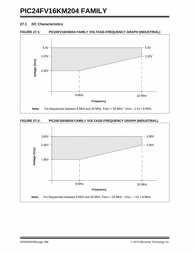
PIC24FV16KM204 FAMILY
27.1 DC Characteristics
FIGURE 27-1: PIC24FV16KM204 FAMILY VOLTAGE-FREQUENCY GRAPH (INDUSTRIAL)
FIGURE 27-2: PIC24F16KM204 FAMILY VOLTAGE-FREQUENCY GRAPH (INDUSTRIAL)
Frequency
Vo
ltag
e (
VD
D)
2.00V
32 MHz
5.5V
3.20V
5.5V
8 MHz
3.20V
Note: For frequencies between 8 MHz and 32 MHz, FMAX = 20 MHz * (VDD – 2.0) + 8 MHz.
Frequency
Vo
ltag
e (
VD
D)
1.80V
32 MHz
3.60V
3.00V
3.60V
8 MHz
3.00V
Note: For frequencies between 8 MHz and 32 MHz, FMAX = 20 MHz * (VDD – 1.8) + 8 MHz.
DS30003030B-page 266 2013 Microchip Technology Inc.
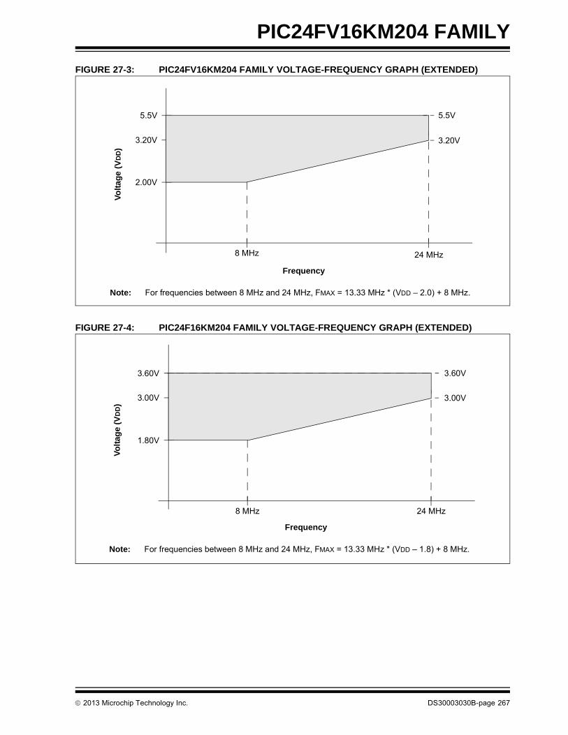
PIC24FV16KM204 FAMILY
FIGURE 27-3: PIC24FV16KM204 FAMILY VOLTAGE-FREQUENCY GRAPH (EXTENDED)
FIGURE 27-4: PIC24F16KM204 FAMILY VOLTAGE-FREQUENCY GRAPH (EXTENDED)
Frequency
Vo
lta
ge
(V
DD
)
2.00V
24 MHz
5.5V
3.20V
5.5V
8 MHz
3.20V
Note: For frequencies between 8 MHz and 24 MHz, FMAX = 13.33 MHz * (VDD – 2.0) + 8 MHz.
Frequency
Vo
ltag
e (
VD
D)
1.80V
24 MHz
3.60V
3.00V
3.60V
8 MHz
3.00V
Note: For frequencies between 8 MHz and 24 MHz, FMAX = 13.33 MHz * (VDD – 1.8) + 8 MHz.
2013 Microchip Technology Inc. DS30003030B-page 267
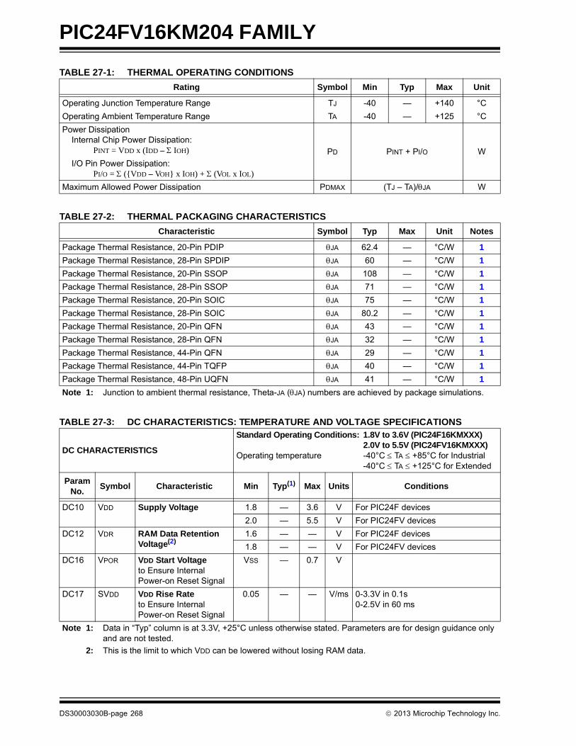
PIC24FV16KM204 FAMILY
TABLE 27-1: THERMAL OPERATING CONDITIONS
Rating Symbol Min Typ Max Unit
Operating Junction Temperature Range TJ -40 — +140 °C
Operating Ambient Temperature Range TA -40 — +125 °C
Power Dissipation Internal Chip Power Dissipation:
PINT = VDD x (IDD – IOH) PD PINT + PI/O W
I/O Pin Power Dissipation:PI/O = (VDD – VOH x IOH) + (VOL x IOL)
Maximum Allowed Power Dissipation PDMAX (TJ – TA)/JA W
TABLE 27-2: THERMAL PACKAGING CHARACTERISTICS
Characteristic Symbol Typ Max Unit Notes
Package Thermal Resistance, 20-Pin PDIP JA 62.4 — °C/W 1
Package Thermal Resistance, 28-Pin SPDIP JA 60 — °C/W 1
Package Thermal Resistance, 20-Pin SSOP JA 108 — °C/W 1
Package Thermal Resistance, 28-Pin SSOP JA 71 — °C/W 1
Package Thermal Resistance, 20-Pin SOIC JA 75 — °C/W 1
Package Thermal Resistance, 28-Pin SOIC JA 80.2 — °C/W 1
Package Thermal Resistance, 20-Pin QFN JA 43 — °C/W 1
Package Thermal Resistance, 28-Pin QFN JA 32 — °C/W 1
Package Thermal Resistance, 44-Pin QFN JA 29 — °C/W 1
Package Thermal Resistance, 44-Pin TQFP JA 40 — °C/W 1
Package Thermal Resistance, 48-Pin UQFN JA 41 — °C/W 1
Note 1: Junction to ambient thermal resistance, Theta-JA (JA) numbers are achieved by package simulations.
TABLE 27-3: DC CHARACTERISTICS: TEMPERATURE AND VOLTAGE SPECIFICATIONS
DC CHARACTERISTICS
Standard Operating Conditions: 1.8V to 3.6V (PIC24F16KMXXX)2.0V to 5.5V (PIC24FV16KMXXX)
Operating temperature -40°C TA +85°C for Industrial -40°C TA +125°C for Extended
ParamNo.
Symbol Characteristic Min Typ(1) Max Units Conditions
DC10 VDD Supply Voltage 1.8 — 3.6 V For PIC24F devices
2.0 — 5.5 V For PIC24FV devices
DC12 VDR RAM Data Retention Voltage(2)
1.6 — — V For PIC24F devices
1.8 — — V For PIC24FV devices
DC16 VPOR VDD Start Voltageto Ensure InternalPower-on Reset Signal
VSS — 0.7 V
DC17 SVDD VDD Rise Rateto Ensure InternalPower-on Reset Signal
0.05 — — V/ms 0-3.3V in 0.1s0-2.5V in 60 ms
Note 1: Data in “Typ” column is at 3.3V, +25°C unless otherwise stated. Parameters are for design guidance only and are not tested.
2: This is the limit to which VDD can be lowered without losing RAM data.
DS30003030B-page 268 2013 Microchip Technology Inc.
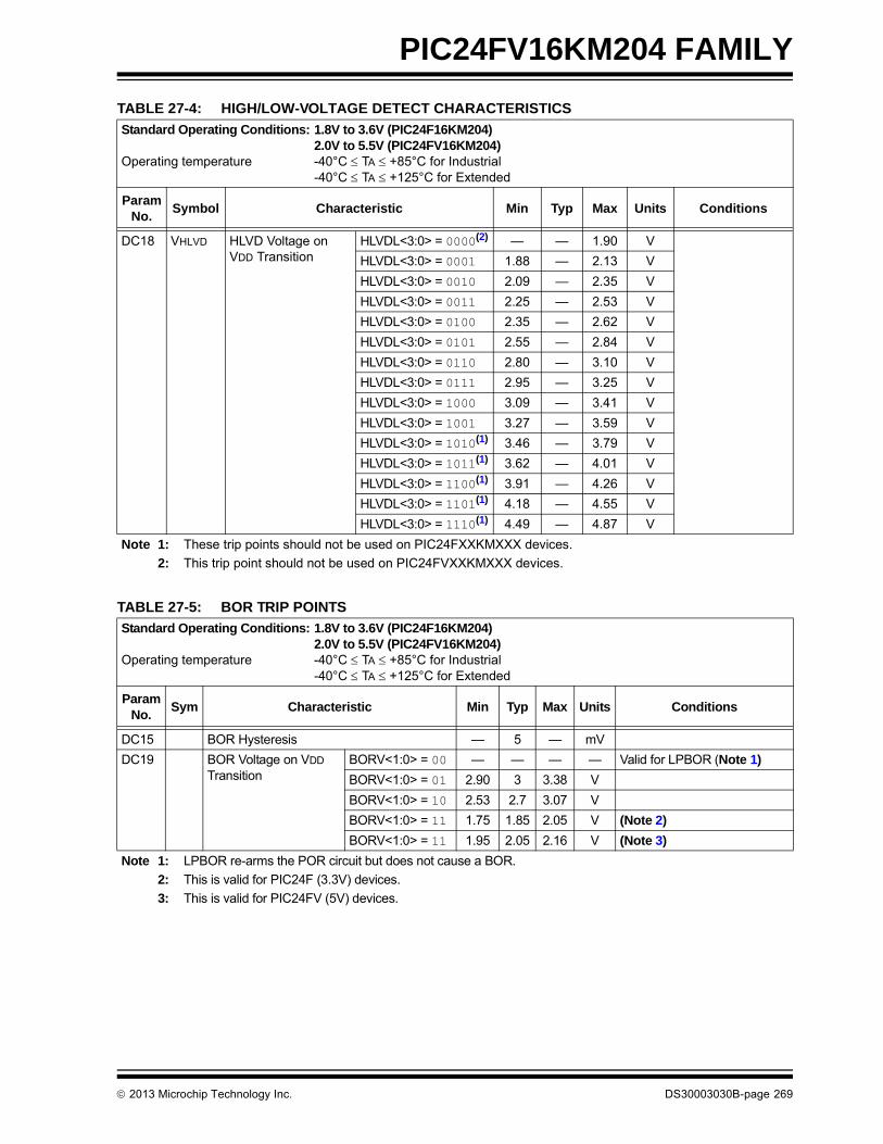
PIC24FV16KM204 FAMILY
TABLE 27-4: HIGH/LOW-VOLTAGE DETECT CHARACTERISTICS
TABLE 27-5: BOR TRIP POINTS
Standard Operating Conditions: 1.8V to 3.6V (PIC24F16KM204)2.0V to 5.5V (PIC24FV16KM204)
Operating temperature -40°C TA +85°C for Industrial-40°C TA +125°C for Extended
Param No.
Symbol Characteristic Min Typ Max Units Conditions
DC18 VHLVD HLVD Voltage on VDD Transition
HLVDL<3:0> = 0000(2) — — 1.90 V
HLVDL<3:0> = 0001 1.88 — 2.13 V
HLVDL<3:0> = 0010 2.09 — 2.35 V
HLVDL<3:0> = 0011 2.25 — 2.53 V
HLVDL<3:0> = 0100 2.35 — 2.62 V
HLVDL<3:0> = 0101 2.55 — 2.84 V
HLVDL<3:0> = 0110 2.80 — 3.10 V
HLVDL<3:0> = 0111 2.95 — 3.25 V
HLVDL<3:0> = 1000 3.09 — 3.41 V
HLVDL<3:0> = 1001 3.27 — 3.59 V
HLVDL<3:0> = 1010(1) 3.46 — 3.79 V
HLVDL<3:0> = 1011(1) 3.62 — 4.01 V
HLVDL<3:0> = 1100(1) 3.91 — 4.26 V
HLVDL<3:0> = 1101(1) 4.18 — 4.55 V
HLVDL<3:0> = 1110(1) 4.49 — 4.87 V
Note 1: These trip points should not be used on PIC24FXXKMXXX devices.
2: This trip point should not be used on PIC24FVXXKMXXX devices.
Standard Operating Conditions: 1.8V to 3.6V (PIC24F16KM204)2.0V to 5.5V (PIC24FV16KM204)
Operating temperature -40°C TA +85°C for Industrial-40°C TA +125°C for Extended
Param No.
Sym Characteristic Min Typ Max Units Conditions
DC15 BOR Hysteresis — 5 — mV
DC19 BOR Voltage on VDD Transition
BORV<1:0> = 00 — — — — Valid for LPBOR (Note 1)
BORV<1:0> = 01 2.90 3 3.38 V
BORV<1:0> = 10 2.53 2.7 3.07 V
BORV<1:0> = 11 1.75 1.85 2.05 V (Note 2)
BORV<1:0> = 11 1.95 2.05 2.16 V (Note 3)
Note 1: LPBOR re-arms the POR circuit but does not cause a BOR.
2: This is valid for PIC24F (3.3V) devices.
3: This is valid for PIC24FV (5V) devices.
2013 Microchip Technology Inc. DS30003030B-page 269

PIC24FV16KM204 FAMILY
TABLE 27-6: DC CHARACTERISTICS: OPERATING CURRENT (IDD)
DC CHARACTERISTICS
Standard Operating Conditions: 1.8V to 3.6V (PIC24F16KMXXX)2.0V to 5.5V (PIC24FV16KMXXX)
Operating temperature -40°C TA +85°C for Industrial -40°C TA +125°C for Extended
Parameter No. Device Typical Max Units Conditions
IDD Current
D20 PIC24FV16KMXXX 269 450 µA 2.0V
0.5 MIPS,FOSC = 1 MHz(1)
465 830 µA 5.0V
PIC24F16KMXXX 200 330 µA 1.8V
410 750 µA 3.3V
DC22 PIC24FV16KMXXX 490 — µA 2.0V
1 MIPS,FOSC = 2 MHz(1)
880 — µA 5.0V
PIC24F16KMXXX 407 — µA 1.8V
800 — µA 3.3V
DC24 PIC24FV16KMXXX 13.0 15.0 mA 5.0V 16 MIPS,FOSC = 32 MHz(1)
PIC24F16KMXXX 12.0 13.0 mA 3.3V
DC26 PIC24FV16KMXXX 2.0 — mA 2.0V
FRC (4 MIPS), FOSC = 8 MHz
3.5 — mA 5.0V
PIC24F16KMXXX 1.80 — mA 1.8V
3.40 — mA 3.3V
DC30 PIC24FV16KMXXX 48.0 250 µA 2.0V
LPRC (15.5 KIPS),FOSC = 31 kHz
75.0 275 µA 5.0V
PIC24F16KMXXX 8.1 28.0 µA 1.8V
13.50 55.00 µA 3.3V
Legend: Unshaded rows represent PIC24F16KMXXX devices and shaded rows represent PIC24FV16KMXXX devices.
Note 1: The oscillator is in External Clock mode (FOSCSEL<2:0> = 010, FOSC<1:0> = 00).
DS30003030B-page 270 2013 Microchip Technology Inc.
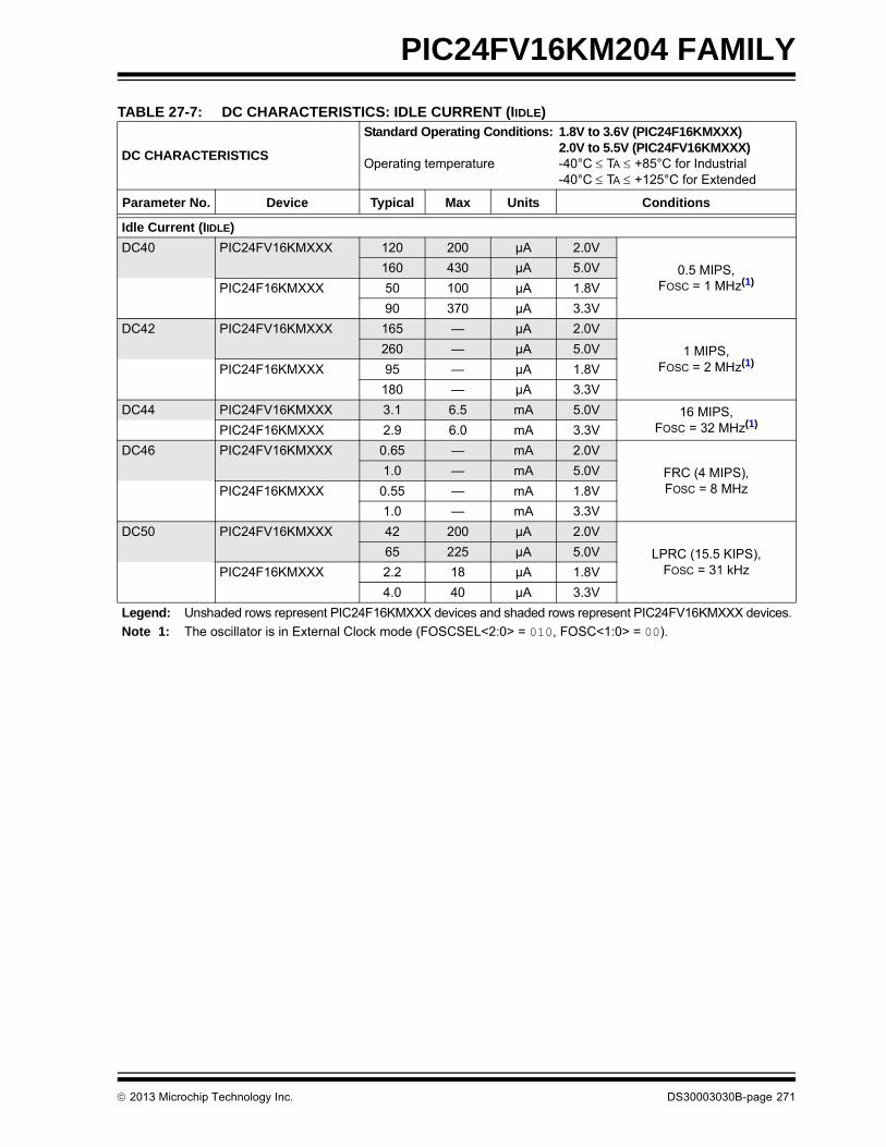
PIC24FV16KM204 FAMILY
TABLE 27-7: DC CHARACTERISTICS: IDLE CURRENT (IIDLE)
DC CHARACTERISTICS
Standard Operating Conditions: 1.8V to 3.6V (PIC24F16KMXXX)2.0V to 5.5V (PIC24FV16KMXXX)
Operating temperature -40°C TA +85°C for Industrial -40°C TA +125°C for Extended
Parameter No. Device Typical Max Units Conditions
Idle Current (IIDLE)
DC40 PIC24FV16KMXXX 120 200 µA 2.0V
0.5 MIPS, FOSC = 1 MHz(1)
160 430 µA 5.0V
PIC24F16KMXXX 50 100 µA 1.8V
90 370 µA 3.3V
DC42 PIC24FV16KMXXX 165 — µA 2.0V
1 MIPS,FOSC = 2 MHz(1)
260 — µA 5.0V
PIC24F16KMXXX 95 — µA 1.8V
180 — µA 3.3V
DC44 PIC24FV16KMXXX 3.1 6.5 mA 5.0V 16 MIPS, FOSC = 32 MHz(1)
PIC24F16KMXXX 2.9 6.0 mA 3.3V
DC46 PIC24FV16KMXXX 0.65 — mA 2.0V
FRC (4 MIPS), FOSC = 8 MHz
1.0 — mA 5.0V
PIC24F16KMXXX 0.55 — mA 1.8V
1.0 — mA 3.3V
DC50 PIC24FV16KMXXX 42 200 µA 2.0V
LPRC (15.5 KIPS), FOSC = 31 kHz
65 225 µA 5.0V
PIC24F16KMXXX 2.2 18 µA 1.8V
4.0 40 µA 3.3V
Legend: Unshaded rows represent PIC24F16KMXXX devices and shaded rows represent PIC24FV16KMXXX devices.
Note 1: The oscillator is in External Clock mode (FOSCSEL<2:0> = 010, FOSC<1:0> = 00).
2013 Microchip Technology Inc. DS30003030B-page 271
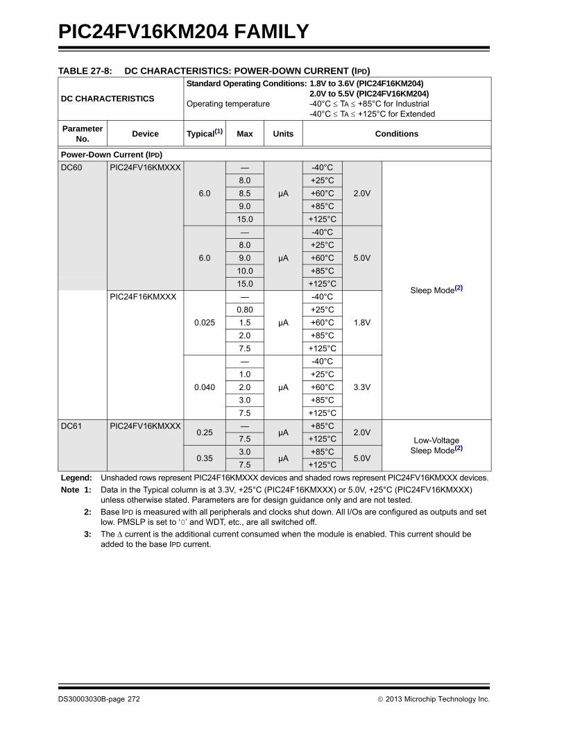
PIC24FV16KM204 FAMILY
TABLE 27-8: DC CHARACTERISTICS: POWER-DOWN CURRENT (IPD)
DC CHARACTERISTICS
Standard Operating Conditions: 1.8V to 3.6V (PIC24F16KM204)2.0V to 5.5V (PIC24FV16KM204)
Operating temperature -40°C TA +85°C for Industrial-40°C TA +125°C for Extended
Parameter No.
Device Typical(1) Max Units Conditions
Power-Down Current (IPD)
DC60 PIC24FV16KMXXX
6.0
—
µA
-40°C
2.0V
Sleep Mode(2)
8.0 +25°C
8.5 +60°C
9.0 +85°C
15.0 +125°C
6.0
—
µA
-40°C
5.0V
8.0 +25°C
9.0 +60°C
10.0 +85°C
15.0 +125°C
PIC24F16KMXXX
0.025
—
µA
-40°C
1.8V
0.80 +25°C
1.5 +60°C
2.0 +85°C
7.5 +125°C
0.040
—
µA
-40°C
3.3V
1.0 +25°C
2.0 +60°C
3.0 +85°C
7.5 +125°C
DC61 PIC24FV16KMXXX0.25
—µA
+85°C2.0V
Low-VoltageSleep Mode(2)
7.5 +125°C
0.353.0
µA+85°C
5.0V7.5 +125°C
Legend: Unshaded rows represent PIC24F16KMXXX devices and shaded rows represent PIC24FV16KMXXX devices.
Note 1: Data in the Typical column is at 3.3V, +25°C (PIC24F16KMXXX) or 5.0V, +25°C (PIC24FV16KMXXX) unless otherwise stated. Parameters are for design guidance only and are not tested.
2: Base IPD is measured with all peripherals and clocks shut down. All I/Os are configured as outputs and set low. PMSLP is set to ‘0’ and WDT, etc., are all switched off.
3: The current is the additional current consumed when the module is enabled. This current should be added to the base IPD current.
DS30003030B-page 272 2013 Microchip Technology Inc.

PIC24FV16KM204 FAMILY
Module Differential Current (IPD)(3)
DC71 PIC24FV16KMXXX 0.50 — µA 2.0VWatchdog Timer
Current: WDT
0.70 1.5 µA 5.0V
PIC24F16KMXXX 0.50 — µA 1.8V
0.70 1.5 µA 3.3V
DC72 PIC24FV16KMXXX 0.80 — µA 2.0V 32 kHz Crystal with RTCC, DSWDT or Timer1:
SOSC(SOSCSEL = 0)
1.50 2.0 µA 5.0V
PIC24F16KMXXX 0.70 — µA 1.8V
1.0 1.5 µA 3.3V
DC75 PIC24FV16KMXXX 5.4 — µA 2.0V
HLVD8.1 14.0 µA 5.0V
PIC24F16KMXXX 4.9 — µA 1.8V
7.5 14.0 µA 3.3V
DC76 PIC24FV16KMXXX 5.6 — µA 2.0V
BOR6.5 11.2 µA 5.0V
PIC24F16KMXXX 5.6 — µA 1.8V
6.0 11.2 µA 3.3V
DC78 PIC24FV16KMXXX 0.03 — µA 2.0V
Low-Power BOR:LPBOR
0.05 0.3 µA 5.0V
PIC24F16KMXXX 0.03 — µA 1.8V
0.05 0.3 µA 3.3V
TABLE 27-8: DC CHARACTERISTICS: POWER-DOWN CURRENT (IPD) (CONTINUED)
DC CHARACTERISTICS
Standard Operating Conditions: 1.8V to 3.6V (PIC24F16KM204)2.0V to 5.5V (PIC24FV16KM204)
Operating temperature -40°C TA +85°C for Industrial-40°C TA +125°C for Extended
Parameter No.
Device Typical(1) Max Units Conditions
Legend: Unshaded rows represent PIC24F16KMXXX devices and shaded rows represent PIC24FV16KMXXX devices.
Note 1: Data in the Typical column is at 3.3V, +25°C (PIC24F16KMXXX) or 5.0V, +25°C (PIC24FV16KMXXX) unless otherwise stated. Parameters are for design guidance only and are not tested.
2: Base IPD is measured with all peripherals and clocks shut down. All I/Os are configured as outputs and set low. PMSLP is set to ‘0’ and WDT, etc., are all switched off.
3: The current is the additional current consumed when the module is enabled. This current should be added to the base IPD current.
2013 Microchip Technology Inc. DS30003030B-page 273

PIC24FV16KM204 FAMILY
TABLE 27-9: DC CHARACTERISTICS: I/O PIN INPUT SPECIFICATIONS
DC CHARACTERISTICS
Standard Operating Conditions: 1.8V to 3.6V (PIC24F16KM204)2.0V to 5.5V (PIC24FV16KM204)
Operating temperature -40°C TA +85°C for Industrial-40°C TA +125°C for Extended
Param No.
Sym Characteristic Min Typ(1) Max Units Conditions
VIL Input Low Voltage(4)
DI10 I/O Pins VSS — 0.2 VDD V
DI15 MCLR VSS — 0.2 VDD V
DI16 OSCI (XT mode) VSS — 0.2 VDD V
DI17 OSCI (HS mode) VSS — 0.2 VDD V
DI18 I/O Pins with I2C™ Buffer VSS — 0.3 VDD V SMBus disabled
DI19 I/O Pins with SMBus Buffer VSS — 0.8 V SMBus enabled
VIH Input High Voltage(4,5)
DI20 I/O Pins: with Analog Functions Digital Only
0.8 VDD
0.8 VDD
——
VDD
VDD
VV
DI25 MCLR 0.8 VDD — VDD V
DI26 OSCI (XT mode) 0.7 VDD — VDD V
DI27 OSCI (HS mode) 0.7 VDD — VDD V
DI28 I/O Pins with I2C Buffer: with Analog Functions Digital Only
0.7 VDD
0.7 VDD
——
VDD
VDD
VV
DI29 I/O Pins with SMBus 2.1 — VDD V 2.5V VPIN VDD
DI30 ICNPU CNx Pull-up Current 50 250 500 A VDD = 3.3V, VPIN = VSS
DI31 IPU Maximum Load Current for Digital High Detection w/Internal Pull-up
— — 30 A VDD = 2.0V
— — 1000 A VDD = 3.3V
IIL Input Leakage Current(2,3)
DI50 I/O Ports — 0.050 ±0.100 A VSS VPIN VDD,Pin at high-impedance
DI51 Pins with OAxOUT Functions (RB15 and RB3)
— 0.100 ±0.200 A VSS VPIN VDD,Pin at high-impedance
Note 1: Data in “Typ” column is at 3.3V, +25°C unless otherwise stated.
2: The leakage current on the MCLR pin is strongly dependent on the applied voltage level. The specified levels represent normal operating conditions. Higher leakage current may be measured at different input voltages.
3: Negative current is defined as current sourced by the pin.
4: Refer to Table 1-4 and Table 1-5 for I/O pin buffer types.
5: VIH requirements are met when the internal pull-ups are enabled.
DS30003030B-page 274 2013 Microchip Technology Inc.

PIC24FV16KM204 FAMILY
TABLE 27-10: DC CHARACTERISTICS: I/O PIN OUTPUT SPECIFICATIONS
DC CHARACTERISTICS
Standard Operating Conditions: 1.8V to 3.6V (PIC24F16KM204)2.0V to 5.5V (PIC24FV16KM204)
Operating temperature -40°C TA +85°C for Industrial-40°C TA +125°C for Extended
Param No.
Sym Characteristic Min Typ(1) Max Units Conditions
VOL Output Low Voltage
DO10 All I/O Pins — — 0.4 V IOL = 8.0 mA VDD = 4.5V
— — 0.4 V IOL = 4.0 mA VDD = 3.6V
— — 0.4 V IOL = 3.5 mA VDD = 2.0V
DO16 OSC2/CLKO — — 0.4 V IOL = 2.0 mA VDD = 4.5V
— — 0.4 V IOL = 1.2 mA VDD = 3.6V
— — 0.4 V IOL = 0.4 mA VDD = 2.0V
VOH Output High Voltage
DO20 All I/O Pins 3.8 — — V IOH = -3.5 mA VDD = 4.5V
3 — — V IOH = -3.0 mA VDD = 3.6V
1.6 — — V IOH = -1.0 mA VDD = 2.0V
DO26 OSC2/CLKO 3.8 — — V IOH = -2.0 mA VDD = 4.5V
3 — — V IOH = -1.0 mA VDD = 3.6V
1.6 — — V IOH = -0.5 mA VDD = 2.0V
Note 1: Data in “Typ” column is at 3.3V, +25°C unless otherwise stated. Parameters are for design guidance only and are not tested.
TABLE 27-11: DC CHARACTERISTICS: PROGRAM MEMORY
DC CHARACTERISTICS
Standard Operating Conditions: 1.8V to 3.6V (PIC24F16KM204)2.0V to 5.5V (PIC24FV16KM204)
Operating temperature -40°C TA +85°C for Industrial-40°C TA +125°C for Extended
ParamNo.
Sym Characteristic Min Typ(1) Max Units Conditions
Program Flash Memory
D130 EP Cell Endurance 10,000(2) — — E/W
D131 VPR VDD for Read VMIN — 3.6 V VMIN = Minimum operating voltage
D133A TIW Self-Timed Write Cycle Time
— 2 — ms
D134 TRETD Characteristic Retention 40 — — Year Provided no other specifications are violated
D135 IDDP Supply Current During Programming
— 10 — mA
Note 1: Data in “Typ” column is at 3.3V, +25°C unless otherwise stated.
2: Self-write and block erase.
2013 Microchip Technology Inc. DS30003030B-page 275

PIC24FV16KM204 FAMILY
TABLE 27-13: DC CHARACTERISTICS: COMPARATOR
TABLE 27-14: DC CHARACTERISTICS: COMPARATOR VOLTAGE REFERENCE
TABLE 27-12: DC CHARACTERISTICS: DATA EEPROM MEMORY
DC CHARACTERISTICS
Standard Operating Conditions: 1.8V to 3.6V (PIC24F16KM204)2.0V to 5.5V (PIC24FV16KM204)
Operating temperature -40°C TA +85°C for Industrial-40°C TA +125°C for Extended
ParamNo.
Sym Characteristic Min Typ(1) Max Units Conditions
Data EEPROM Memory
D140 EPD Cell Endurance 100,000 — — E/W
D141 VPRD VDD for Read VMIN — 3.6 V VMIN = Minimum operating voltage
D143A TIWD Self-Timed Write Cycle Time
— 4 — ms
D143B TREF Number of Total Write/Erase Cycles Before Refresh
— 10M — E/W
D144 TRETDD Characteristic Retention 40 — — Year Provided no other specifications are violated
D145 IDDPD Supply Current During Programming
— 7 — mA
Note 1: Data in “Typ” column is at 3.3V, +25°C unless otherwise stated.
DC CHARACTERISTICS
Standard Operating Conditions: 1.8V to 3.6V (PIC24F16KM204)2.0V to 5.5V (PIC24FV16KM204)
Operating temperature -40°C TA +85°C for Industrial-40°C TA +125°C for Extended
ParamNo.
Symbol Characteristic Min Typ Max Units Conditions
D300 VIOFF Input Offset Voltage — 20 40 mV
D301 VICM Input Common-Mode Voltage 0 — VDD V
D302 CMRR Common-Mode Rejection Ratio
55 — — dB
DC CHARACTERISTICS
Standard Operating Conditions: 1.8V to 3.6V (PIC24F16KM204)2.0V to 5.5V (PIC24FV16KM204)
Operating temperature -40°C TA +85°C for Industrial-40°C TA +125°C for Extended
ParamNo.
Symbol Characteristic Min Typ Max Units Conditions
VRD310 CVRES Resolution — — VDD/32 LSb
VRD311 CVRAA Absolute Accuracy — — 1 LSb AVDD = 3.3V-5.5V
VRD312 CVRUR Unit Resistor Value (R) — 2k —
DS30003030B-page 276 2013 Microchip Technology Inc.

PIC24FV16KM204 FAMILY
TABLE 27-15: INTERNAL VOLTAGE REGULATOR SPECIFICATIONS
Operating Conditions: -40°C < TA < +85°C (unless otherwise stated) -40°C TA +125°C for Extended
ParamNo.
Symbol Characteristics Min Typ Max Units Comments
VBG Band Gap Reference Voltage
0.973 1.024 1.075 V VDD > 4.5V for 4*VBG referenceVDD > 2.3V for 2*VBG reference
TBG Band Gap Reference Start-up Time
— 1 — ms
VRGOUT Regulator Output Voltage 3.1 3.3 3.6 V
CEFC External Filter Capacitor Value
4.7 10 — F Series resistance < 3 Ohm recommended; < 5 Ohm is required.
VLVR Low-Voltage Regulator Output Voltage
— 2.6 — V
TABLE 27-16: CTMU CURRENT SOURCE SPECIFICATIONS
DC CHARACTERISTICS
Standard Operating Conditions: 1.8V to 3.6V (PIC24F16KM204)2.0V to 5.5V (PIC24FV16KM204)
Operating temperature -40°C TA +85°C for Industrial-40°C TA +125°C for Extended
ParamNo.
Sym Characteristic Min Typ(1) Max Units Comments Conditions
IOUT1 CTMU Current Source, Base Range
— 550 — nA CTMUCON1L<1:0> = 01
2.5V < VDD < VDDMAX
IOUT2 CTMU Current Source, 10x Range
— 5.5 — A CTMUCON1L<1:0> = 10
IOUT3 CTMU Current Source, 100x Range
— 55 — A CTMUCON1L<1:0> = 11
IOUT4 CTMU Current Source, 1000x Range
— 550 — A CTMUCON1L<1:0> = 00(Note 2)
VF Temperature Diode Forward Voltage
— .76 — V
V Voltage Change per Degree Celsius
— 1.6 — mV/°C
Note 1: Nominal value at the center point of the current trim range (CTMUCON1L<7:2> = 000000). On PIC24F16KM parts, the current output is limited to the typical current value when IOUT4 is chosen.
2: Do not use this current range with a temperature sensing diode.
2013 Microchip Technology Inc. DS30003030B-page 277

PIC24FV16KM204 FAMILY
TABLE 27-17: OPERATIONAL AMPLIFIER SPECIFICATIONS
DC CHARACTERISTICS
Standard Operating Conditions: 1.8V to 3.6V (PIC24F16KM204)2.0V to 5.5V (PIC24FV16KM204)
Operating temperature -40°C TA +85°C for Industrial-40°C TA +125°C for Extended
ParamNo.
Sym Characteristic Min Typ(1) Max Units Comments
GBWP Gain Bandwidth Product
— 5 — MHz SPDSEL = 1
— 0.5 — MHz SPDSEL = 0
SR Slew Rate — 1.2 — V/µs SPDSEL = 1
— 0.3 — V/µs SPDSEL = 0
AOL DC Open-Loop Gain — 90 — dB
VIOFF Input Offset Voltage — ±2 ±10 mV
VIBC Input Bias Current — — — nA (Note 1)
VICM Common-Mode Input Voltage Range
AVSS — AVDD V
CMRR Common-Mode Rejection Ratio
— 60 — db
PSRR Power Supply Rejection Ratio
— 60 — dB
VOR Output Voltage Range
AVSS + 200 AVSS + 5 to AVDD – 5
AVDD – 200 mV 0.5V input overdrive, no output loading
Note 1: The op amps use CMOS input circuitry with negligible input bias current. The maximum “effective bias current” is the I/O pin leakage specified by electrical Parameter DI50.
DS30003030B-page 278 2013 Microchip Technology Inc.

PIC24FV16KM204 FAMILY
27.2 AC Characteristics and Timing Parameters
The information contained in this section defines the PIC24FV16KM204 family AC characteristics and timingparameters.
TABLE 27-18: TEMPERATURE AND VOLTAGE SPECIFICATIONS – AC
FIGURE 27-5: LOAD CONDITIONS FOR DEVICE TIMING SPECIFICATIONS
TABLE 27-19: CAPACITIVE LOADING REQUIREMENTS ON OUTPUT PINS
AC CHARACTERISTICS
Standard Operating Conditions: 1.8V to 3.6V Operating temperature -40°C TA +85°C for Industrial
-40°C TA +125°C for ExtendedOperating voltage VDD range as described in Section 27.1 “DC Characteristics”.
Param No.
Symbol Characteristic Min Typ(1) Max Units Conditions
DO50 COSC2 OSCO/CLKO Pin — — 15 pF In XT and HS modes when External Clock is used to drive OSCI
DO56 CIO All I/O Pins and OSCO — — 50 pF EC mode
DO58 CB SCLx, SDAx — — 400 pF In I2C™ mode
Note 1: Data in “Typ” column is at 3.3V, +25°C unless otherwise stated. Parameters are for design guidance only and are not tested.
VDD/2
CL
RL
Pin
Pin
VSS
VSS
CL
RL = 464CL = 50 pF for all pins except OSCO
15 pF for OSCO output
Load Condition 1 – for all pins except OSCO Load Condition 2 – for OSCO
2013 Microchip Technology Inc. DS30003030B-page 279

PIC24FV16KM204 FAMILY
FIGURE 27-6: EXTERNAL CLOCK TIMING
OSCI
CLKO
Q4 Q1 Q2 Q3 Q4 Q1
OS20
OS25OS30 OS30
OS40 OS41
OS31OS31
Q1 Q2 Q3 Q4 Q2 Q3
TABLE 27-20: EXTERNAL CLOCK TIMING REQUIREMENTS
AC CHARACTERISTICS
Standard Operating Conditions: 1.8V to 3.6V (PIC24F16KM204)2.0V to 5.5V (PIC24FV16KM204)
Operating temperature -40°C TA +85°C for Industrial-40°C TA +125°C for Extended
ParamNo.
Sym Characteristic Min Typ(1) Max Units Conditions
OS10 FOSC External CLKI Frequency(External Clocks allowed only in EC mode)
DC4
DC4
————
328246
MHzMHzMHzMHz
EC, -40°C < TA < +85°CECPLL, -40°C < TA < +85°CEC, -40°C < TA < +125°CECPLL, -40°C < TA < +125°C
Oscillator Frequency 0.244431
—————
4258633
MHzMHzMHzMHzkHz
XTHSXTPLL, -40°C < TA < +85°CXTPLL, -40°C < TA < +125°CSOSC
OS20 TOSC TOSC = 1/FOSC — — — — See Parameter OS10 for FOSC value
OS25 TCY Instruction Cycle Time(2) 62.5 — DC ns
OS30 TosL,TosH
External Clock in (OSCI)High or Low Time
0.45 x TOSC — — ns EC
OS31 TosR,TosF
External Clock in (OSCI)Rise or Fall Time
— — 20 ns EC
OS40 TckR CLKO Rise Time(3) — 6 10 ns
OS41 TckF CLKO Fall Time(3) — 6 10 ns
Note 1: Data in “Typ” column is at 3.3V, +25°C unless otherwise stated. Parameters are for design guidance only and are not tested.
2: Instruction cycle period (TCY) equals two times the input oscillator time base period. All specified values are based on characterization data for that particular oscillator type, under standard operating conditions, with the device executing code. Exceeding these specified limits may result in an unstable oscillator operation and/or higher than expected current consumption. All devices are tested to operate at “Min.” values with an External Clock applied to the OSCI/CLKI pin. When an External Clock input is used, the “Max.” cycle time limit is “DC” (no clock) for all devices.
3: Measurements are taken in EC mode. The CLKO signal is measured on the OSCO pin. CLKO is low for the Q1-Q2 period (1/2 TCY) and high for the Q3-Q4 period (1/2 TCY).
DS30003030B-page 280 2013 Microchip Technology Inc.

PIC24FV16KM204 FAMILY
TABLE 27-21: PLL CLOCK TIMING SPECIFICATIONS
AC CHARACTERISTICS
Standard Operating Conditions: 1.8V to 3.6V (PIC24F16KM204)2.0V to 5.5V (PIC24FV16KM204)
Operating temperature -40°C TA +85°C for Industrial-40°C TA +125°C for Extended
ParamNo.
Sym Characteristic(1) Min Typ(2) Max Units Conditions
OS50 FPLLI PLL Input Frequency Range
4 — 8 MHz ECPLL, HSPLL modes, -40°C TA +85°C
OS51 FSYS PLL Output Frequency Range
16 — 32 MHz -40°C TA +85°C
OS52 TLOCK PLL Start-up Time (Lock Time)
— 1 2 ms
OS53 DCLK CLKO Stability (Jitter) -2 1 2 % Measured over 100 ms period
Note 1: These parameters are characterized but not tested in manufacturing.
2: Data in “Typ” column is at 3.3V, +25°C unless otherwise stated. Parameters are for design guidance only and are not tested.
TABLE 27-22: INTERNAL RC OSCILLATOR ACCURACY
AC CHARACTERISTICS
Standard Operating Conditions: 1.8V to 3.6V (PIC24F16KM204)2.0V to 5.5V (PIC24FV16KM204)
Operating temperature -40°C TA +85°C for Industrial-40°C TA +125°C for Extended
Param No.
Characteristic Min Typ Max Units Conditions
F20 FRC @ 8 MHz(1) -2 — +2 % +25°C 3.0V VDD 3.6V, F device3.2V VDD 5.5V, FV device
-5 — +5 % -40°C TA +125°C 1.8V VDD 3.6V, F device2.0V VDD 5.5V, FV device
F21 LPRC @ 31 kHz(2) -15 — +15 % -40°C TA +125°C 1.8V VDD 3.6V, F device2.0V VDD 5.5V, FV device
Note 1: The frequency is calibrated at +25°C and 3.3V. The OSCTUN bits can be used to compensate for temperature drift.
2: The change of LPRC frequency as VDD changes.
TABLE 27-23: INTERNAL RC OSCILLATOR SPECIFICATIONS
AC CHARACTERISTICS
Standard Operating Conditions: 1.8V to 3.6V (PIC24F16KM204)2.0V to 5.5V (PIC24FV16KM204)
Operating temperature -40°C TA +85°C for Industrial-40°C TA +125°C for Extended
ParamNo.
Sym Characteristic Min Typ Max Units Conditions
TFRC FRC Start-up Time — 5 — s
TLPRC LPRC Start-up Time — 70 — s
2013 Microchip Technology Inc. DS30003030B-page 281

PIC24FV16KM204 FAMILY
FIGURE 27-7: CLKO AND I/O TIMING CHARACTERISTICS
Note: Refer to Figure 27-5 for load conditions.
I/O Pin(Input)
I/O Pin(Output)
DI35
Old Value New Value
DI40
DO31DO32
TABLE 27-24: CLKO AND I/O TIMING REQUIREMENTS
AC CHARACTERISTICS
Standard Operating Conditions: 1.8V to 3.6V (PIC24F16KM204)2.0V to 5.5V (PIC24FV16KM204)
Operating temperature -40°C TA +85°C for Industrial-40°C TA +125°C for Extended
ParamNo.
Sym Characteristic Min Typ(1) Max Units Conditions
DO31 TIOR Port Output Rise Time — 10 25 ns
DO32 TIOF Port Output Fall Time — 10 25 ns
DI35 TINP INTx Pin High or Low Time (output)
20 — — ns
DI40 TRBP CNx High or Low Time (input) 2 — — TCY
Note 1: Data in “Typ” column is at 3.3V, +25°C unless otherwise stated.
DS30003030B-page 282 2013 Microchip Technology Inc.

PIC24FV16KM204 FAMILY
FIGURE 27-8: RESET, WATCHDOG TIMER, OSCILLATOR START-UP TIMER AND POWER-UP TIMER TIMING CHARACTERISTICS
VDD
MCLR
InternalPOR
PWRT
SYSRST
SystemClock
WatchdogTimer Reset
SY10
SY20
SY13
I/O Pins
SY13
SY35
SY11
SY12
2013 Microchip Technology Inc. DS30003030B-page 283

PIC24FV16KM204 FAMILY
FIGURE 27-9: BROWN-OUT RESET CHARACTERISTICS
TABLE 27-25: RESET, WATCHDOG TIMER, OSCILLATOR START-UP TIMER, POWER-UP TIMER AND BROWN-OUT RESET TIMING REQUIREMENTS
AC CHARACTERISTICS
Standard Operating Conditions: 1.8V to 3.6V (PIC24F16KM204)2.0V to 5.5V (PIC24FV16KM204)
Operating temperature -40°C TA +85°C for Industrial-40°C TA +125°C for Extended
Param No.
Symbol Characteristic Min. Typ(1) Max. Units Conditions
SY10 TmcL MCLR Pulse Width (low) 2 — — s
SY11 TPWRT Power-up Timer Period 50 64 90 ms
SY12 TPOR Power-on Reset Delay 1 5 10 s
SY13 TIOZ I/O High-Impedance from MCLR Low or Watchdog Timer Reset
— — 100 ns
SY20 TWDT Watchdog Timer Time-out Period
0.85 1.0 1.15 ms 1.32 prescaler
3.4 4.0 4.6 ms 1:128 prescaler
SY25 TBOR Brown-out Reset Pulse Width
1 — — s
SY35 TFSCM Fail-Safe Clock Monitor Delay
— 2.0 2.3 s
SY45 TRST Internal State Reset Time — 5 — s
SY50 TVREG On-Chip Voltage Regulator Output Delay
— 10 — s (Note 2)
SY55 TLOCK PLL Start-up Time — 100 — s
SY65 TOST Oscillator Start-up Time — 1024 — TOSC
SY71 TPM Program Memory Wake-up Time
— 1 — s Sleep wake-up with PMSLP = 0
SY72 TLVR Low-Voltage Regulator Wake-up Time
— 250 — s
Note 1: Data in “Typ” column is at 3.3V, +25°C unless otherwise stated.
2: This applies to PIC24FV16KMXXX devices only.
DC19
Reset (Due to BOR)
VDDCORE
(Device in Brown-out Reset)
(Device not in Brown-out Reset)
TVREG + TRST
DC15
SY25
DS30003030B-page 284 2013 Microchip Technology Inc.

PIC24FV16KM204 FAMILY
TABLE 27-26: COMPARATOR TIMING REQUIREMENTS
TABLE 27-27: COMPARATOR VOLTAGE REFERENCE SETTLING TIME SPECIFICATIONS
FIGURE 27-10: CAPTURE/COMPARE/PWM TIMINGS (MCCPx, SCCPx MODULES)
TABLE 27-28: CAPTURE/COMPARE/PWM REQUIREMENTS (MCCPx, SCCPx MODULES)
ParamNo.
Symbol Characteristic Min Typ Max Units Comments
300 TRESP Response Time*(1) — 150 400 ns
301 TMC2OV Comparator Mode Change to Output Valid*
— — 10 s
* Parameters are characterized but not tested.
Note 1: Response time is measured with one comparator input at (VDD – 1.5)/2, while the other input transitions from VSS to VDD.
ParamNo.
Symbol Characteristic Min Typ Max Units Comments
VR310 TSET Settling Time(1) — — 10 s
Note 1: Settling time is measured while CVRSS = 1 and the CVR<3:0> bits transition from ‘0000’ to ‘1111’.
Param No.
Symbol Characteristic Min Max Units Conditions
50 TCLKL CCPx Time Base Clock Source Low Time TCY/2 — ns
51 TCLKH CCPx Time Base Clock Source High Time TCY/2 — ns
52 TCLK CCPx Time Base Clock Source Period TCY — ns
53 TCCL CCPx Capture or Gating Input Low Time TCLK — ns
54 TCCH CCPx Capture or Gating Input High Time TCLK — ns
55 TCCP CCPx Capture or Gating Input Period 2 * TCLK/N — ns N = Prescale Value (1, 4 or 16)
Note: Refer to Figure 27-5 for load conditions.
CCPx Time Base
50 51
52
Clock Source
CCPx Capture Input (ICx)
53 54
55
and Gating Inputs
2013 Microchip Technology Inc. DS30003030B-page 285

PIC24FV16KM204 FAMILY
FIGURE 27-11: EXAMPLE SPI MASTER MODE TIMING (CKE = 0)
TABLE 27-29: EXAMPLE SPI MODE REQUIREMENTS (MASTER MODE, CKE = 0)
Param No.
Symbol Characteristic Min Max Units Conditions
73 TDIV2SCH, TDIV2SCL
Setup Time of SDIx Data Input to SCKx Edge 20 — ns
74 TSCH2DIL, TSCL2DIL
Hold Time of SDIx Data Input to SCKx Edge 40 — ns
75 TDOR SDOx Data Output Rise Time — 25 ns
76 TDOF SDOx Data Output Fall Time — 25 ns
78 TSCR SCKx Output Rise Time (Master mode) — 25 ns
79 TSCF SCKx Output Fall Time (Master mode) — 25 ns
FSCK SCKx Frequency — 10 MHz
SCKx(CKP = 0)
SCKx(CKP = 1)
SDOx
SDIx
7374
75, 76
7879
7978
MSb LSbbit 6 - - - - - - 1
LSb Inbit 6 - - - - 1
Note: Refer to Figure 27-5 for load conditions.
MSb In
DS30003030B-page 286 2013 Microchip Technology Inc.

PIC24FV16KM204 FAMILY
FIGURE 27-12: EXAMPLE SPI MASTER MODE TIMING (CKE = 1)
TABLE 27-30: EXAMPLE SPI MODE REQUIREMENTS (MASTER MODE, CKE = 1)
Param. No.
Symbol Characteristic Min Max Units Conditions
73 TDIV2SCH,TDIV2SCL
Setup Time of SDIx Data Input to SCKx Edge 35 — ns
74 TSCH2DIL, TSCL2DIL
Hold Time of SDIx Data Input to SCKx Edge 40 — ns
75 TDOR SDOx Data Output Rise Time — 25 ns
76 TDOF SDOx Data Output Fall Time — 25 ns
78 TSCR SCKx Output Rise Time (Master mode) — 25 ns
79 TSCF SCKx Output Fall Time (Master mode) — 25 ns
81 TDOV2SCH,TDOV2SCL
SDOx Data Output Setup to SCKx Edge TCY — ns
FSCK SCKx Frequency — 10 MHz
SCKx(CKP = 0)
SCKx(CKP = 1)
SDOx
SDIx
81
74
75, 76
78
MSb
7973
bit 6 - - - - - - 1
LSb Inbit 6 - - - - 1
LSb
Note: Refer to Figure 27-5 for load conditions.
MSb In
2013 Microchip Technology Inc. DS30003030B-page 287

PIC24FV16KM204 FAMILY
FIGURE 27-13: EXAMPLE SPI SLAVE MODE TIMING (CKE = 0)
TABLE 27-31: EXAMPLE SPI MODE REQUIREMENTS (SLAVE MODE TIMING, CKE = 0)
Param No.
Symbol Characteristic Min Max Units Conditions
70 TSSL2SCH, TSSL2SCL
SSx to SCKx or SCKx Input 3 TCY — ns
70A TSSL2WB SSx to Write to SSPxBUF 3 TCY — ns
71 TSCH SCKx Input High Time (Slave mode)
Continuous 1.25 TCY + 30 — ns
71A Single Byte 40 — ns (Note 1)
72 TSCL SCKx Input Low Time (Slave mode)
Continuous 1.25 TCY + 30 — ns
72A Single Byte 40 — ns (Note 1)
73 TDIV2SCH, TDIV2SCL
Setup Time of SDIx Data Input to SCKx Edge 20 — ns
73A TB2B Last Clock Edge of Byte 1 to the First Clock Edge of Byte 2 1.5 TCY + 40 — ns (Note 2)
74 TSCH2DIL, TSCL2DIL
Hold Time of SDIx Data Input to SCKx Edge 40 — ns
75 TDOR SDOx Data Output Rise Time — 25 ns
76 TDOF SDOx Data Output Fall Time — 25 ns
77 TSSH2DOZ SSx to SDOx Output High-Impedance 10 50 ns
80 TSCH2DOV,TSCL2DOV
SDOx Data Output Valid After SCKx Edge — 50 ns
83 TSCH2SSH,TSCL2SSH
SSx After SCKx Edge 1.5 TCY + 40 — ns
FSCK SCKx Frequency — 10 MHz
Note 1: Requires the use of Parameter 73A.
2: Only if Parameters 71A and 72A are used.
SSx
SCKx(CKP = 0)
SCKx(CKP = 1)
SDOx
SDIx
70
71 72
7374
75, 76 77
80
MSb LSbbit 6 - - - - - - 1
bit 6 - - - - 1 LSb In
83
Note: Refer to Figure 27-5 for load conditions.
MSb In
DS30003030B-page 288 2013 Microchip Technology Inc.
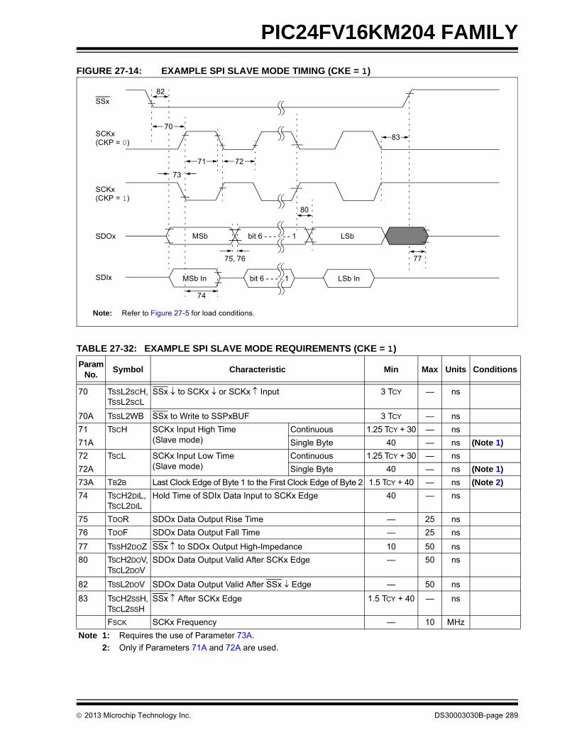
PIC24FV16KM204 FAMILY
FIGURE 27-14: EXAMPLE SPI SLAVE MODE TIMING (CKE = 1)
TABLE 27-32: EXAMPLE SPI SLAVE MODE REQUIREMENTS (CKE = 1)
ParamNo.
Symbol Characteristic Min Max Units Conditions
70 TSSL2SCH, TSSL2SCL
SSx to SCKx or SCKx Input 3 TCY — ns
70A TSSL2WB SSx to Write to SSPxBUF 3 TCY — ns
71 TSCH SCKx Input High Time (Slave mode)
Continuous 1.25 TCY + 30 — ns
71A Single Byte 40 — ns (Note 1)
72 TSCL SCKx Input Low Time (Slave mode)
Continuous 1.25 TCY + 30 — ns
72A Single Byte 40 — ns (Note 1)
73A TB2B Last Clock Edge of Byte 1 to the First Clock Edge of Byte 2 1.5 TCY + 40 — ns (Note 2)
74 TSCH2DIL, TSCL2DIL
Hold Time of SDIx Data Input to SCKx Edge 40 — ns
75 TDOR SDOx Data Output Rise Time — 25 ns
76 TDOF SDOx Data Output Fall Time — 25 ns
77 TSSH2DOZ SSx to SDOx Output High-Impedance 10 50 ns
80 TSCH2DOV,TSCL2DOV
SDOx Data Output Valid After SCKx Edge — 50 ns
82 TSSL2DOV SDOx Data Output Valid After SSx Edge — 50 ns
83 TSCH2SSH,TSCL2SSH
SSx After SCKx Edge 1.5 TCY + 40 — ns
FSCK SCKx Frequency — 10 MHz
Note 1: Requires the use of Parameter 73A.
2: Only if Parameters 71A and 72A are used.
SSx
SCKx(CKP = 0)
SCKx(CKP = 1)
SDOx
71 72
82
SDIx
74
75, 76
MSb bit 6 - - - - - - 1 LSb
77
bit 6 - - - - 1 LSb In
80
83
73
MSb In
Note: Refer to Figure 27-5 for load conditions.
70
2013 Microchip Technology Inc. DS30003030B-page 289

PIC24FV16KM204 FAMILY
FIGURE 27-15: I2C™ BUS START/STOP BITS TIMING
TABLE 27-33: I2C™ BUS START/STOP BITS REQUIREMENTS (SLAVE MODE)
FIGURE 27-16: I2C™ BUS DATA TIMING
Param. No.
Symbol Characteristic Min Max Units Conditions
90 TSU:STA Start Condition Setup Time
100 kHz mode 4700 — ns Only relevant for Repeated Start condition400 kHz mode 600 —
91 THD:STA Start Condition Hold Time
100 kHz mode 4000 — ns After this period, the first clock pulse is generated400 kHz mode 600 —
92 TSU:STO Stop ConditionSetup Time
100 kHz mode 4700 — ns
400 kHz mode 600 —
93 THD:STO Stop ConditionHold Time
100 kHz mode 4000 — ns
400 kHz mode 600 —
Note: Refer to Figure 27-5 for load conditions.
SCLx
SDAx
StartCondition
StopCondition
90
91
92
93
Note: Refer to Figure 27-5 for load conditions.
90
91 92
100
101
103
106 107
109 109110
102
SCLx
SDAx In
SDAxOut
DS30003030B-page 290 2013 Microchip Technology Inc.
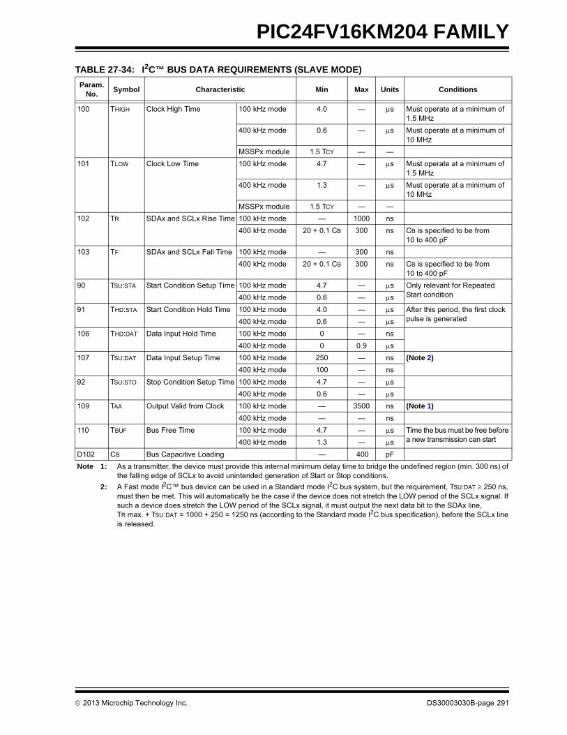
PIC24FV16KM204 FAMILY
TABLE 27-34: I2C™ BUS DATA REQUIREMENTS (SLAVE MODE)
Param. No.
Symbol Characteristic Min Max Units Conditions
100 THIGH Clock High Time 100 kHz mode 4.0 — s Must operate at a minimum of 1.5 MHz
400 kHz mode 0.6 — s Must operate at a minimum of 10 MHz
MSSPx module 1.5 TCY — —
101 TLOW Clock Low Time 100 kHz mode 4.7 — s Must operate at a minimum of 1.5 MHz
400 kHz mode 1.3 — s Must operate at a minimum of 10 MHz
MSSPx module 1.5 TCY — —
102 TR SDAx and SCLx Rise Time 100 kHz mode — 1000 ns
400 kHz mode 20 + 0.1 CB 300 ns CB is specified to be from 10 to 400 pF
103 TF SDAx and SCLx Fall Time 100 kHz mode — 300 ns
400 kHz mode 20 + 0.1 CB 300 ns CB is specified to be from 10 to 400 pF
90 TSU:STA Start Condition Setup Time 100 kHz mode 4.7 — s Only relevant for Repeated Start condition400 kHz mode 0.6 — s
91 THD:STA Start Condition Hold Time 100 kHz mode 4.0 — s After this period, the first clock pulse is generated400 kHz mode 0.6 — s
106 THD:DAT Data Input Hold Time 100 kHz mode 0 — ns
400 kHz mode 0 0.9 s
107 TSU:DAT Data Input Setup Time 100 kHz mode 250 — ns (Note 2)
400 kHz mode 100 — ns
92 TSU:STO Stop Condition Setup Time 100 kHz mode 4.7 — s
400 kHz mode 0.6 — s
109 TAA Output Valid from Clock 100 kHz mode — 3500 ns (Note 1)
400 kHz mode — — ns
110 TBUF Bus Free Time 100 kHz mode 4.7 — s Time the bus must be free before a new transmission can start400 kHz mode 1.3 — s
D102 CB Bus Capacitive Loading — 400 pF
Note 1: As a transmitter, the device must provide this internal minimum delay time to bridge the undefined region (min. 300 ns) of the falling edge of SCLx to avoid unintended generation of Start or Stop conditions.
2: A Fast mode I2C™ bus device can be used in a Standard mode I2C bus system, but the requirement, TSU:DAT 250 ns, must then be met. This will automatically be the case if the device does not stretch the LOW period of the SCLx signal. If such a device does stretch the LOW period of the SCLx signal, it must output the next data bit to the SDAx line,TR max. + TSU:DAT = 1000 + 250 = 1250 ns (according to the Standard mode I2C bus specification), before the SCLx line is released.
2013 Microchip Technology Inc. DS30003030B-page 291

PIC24FV16KM204 FAMILY
FIGURE 27-17: MSSPx I2C™ BUS START/STOP BITS TIMING WAVEFORMS
TABLE 27-35: I2C™ BUS START/STOP BITS REQUIREMENTS (MASTER MODE)
Param.No.
Symbol Characteristic Min Max Units Conditions
90 TSU:STA Start Condition Setup Time
100 kHz mode 2(TOSC)(BRG + 1) — ns Only relevant for Repeated Start condition
400 kHz mode 2(TOSC)(BRG + 1) —
91 THD:STA Start Condition Hold Time
100 kHz mode 2(TOSC)(BRG + 1) — ns After this period, the first clock pulse is generated
400 kHz mode 2(TOSC)(BRG + 1) —
92 TSU:STO Stop ConditionSetup Time
100 kHz mode 2(TOSC)(BRG + 1) ——
ns
400 kHz mode 2(TOSC)(BRG + 1)
93 THD:STO Stop ConditionHold Time
100 kHz mode 2(TOSC)(BRG + 1) — ns
400 kHz mode 2(TOSC)(BRG + 1) —
Note: Refer to Figure 27-5 for load conditions.
SCLx
SDAx
StartCondition
StopCondition
91
90
93
92
DS30003030B-page 292 2013 Microchip Technology Inc.

PIC24FV16KM204 FAMILY
FIGURE 27-18: MSSPx I2C™ BUS DATA TIMING
TABLE 27-36: I2C™ BUS DATA REQUIREMENTS (MASTER MODE)
Param.No.
Symbol Characteristic Min Max Units Conditions
100 THIGH Clock High Time 100 kHz mode 2(TOSC)(BRG + 1) — —
400 kHz mode 2(TOSC)(BRG + 1) — —
101 TLOW Clock Low Time 100 kHz mode 2(TOSC)(BRG + 1) — —
400 kHz mode 2(TOSC)(BRG + 1) — —
102 TR SDAx and SCLx Rise Time
100 kHz mode — 1000 ns CB is specified to be from 10 to 400 pF 400 kHz mode 20 + 0.1 CB 300 ns
103 TF SDAx and SCLx Fall Time
100 kHz mode — 300 ns CB is specified to be from 10 to 400 pF 400 kHz mode 20 + 0.1 CB 300 ns
90 TSU:STA Start Condition Setup Time
100 kHz mode 2(TOSC)(BRG + 1) — — Only relevant for Repeated Start condition400 kHz mode 2(TOSC)(BRG + 1) — —
91 THD:STA Start Condition Hold Time
100 kHz mode 2(TOSC)(BRG + 1) — — After this period, the first clock pulse is generated400 kHz mode 2(TOSC)(BRG + 1) — —
106 THD:DAT Data Input Hold Time
100 kHz mode 0 — ns
400 kHz mode 0 0.9 s
107 TSU:DAT Data Input Setup Time
100 kHz mode 250 — ns (Note 1)
400 kHz mode 100 — ns
92 TSU:STO Stop Condition Setup Time
100 kHz mode 2(TOSC)(BRG + 1) — —
400 kHz mode 2(TOSC)(BRG + 1) — —
109 TAA Output Valid from Clock
100 kHz mode — 3500 ns
400 kHz mode — 1000 ns
110 TBUF Bus Free Time 100 kHz mode 4.7 — s Time the bus must be free before a new transmission can start
400 kHz mode 1.3 — s
D102 CB Bus Capacitive Loading — 400 pF
Note 1: A Fast mode I2C bus device can be used in a Standard mode I2C bus system, but Parameter 107 250 ns must then be met. This will automatically be the case if the device does not stretch the LOW period of the SCLx signal. If such a device does stretch the LOW period of the SCLx signal, it must output the next data bit to the SDAx line, Parameter 102 + Parameter 107 = 1000 + 250 = 1250 ns (for 100 kHz mode), before the SCLx line is released.
Note: Refer to Figure 27-5 for load conditions.
9091 92
100
101
103
106107
109 109 110
102
SCLx
SDAx In
SDAxOut
2013 Microchip Technology Inc. DS30003030B-page 293

PIC24FV16KM204 FAMILY
TABLE 27-37: A/D MODULE SPECIFICATIONS
AC CHARACTERISTICS
Standard Operating Conditions: 1.8V to 3.6V (PIC24F16KM204)2.0V to 5.5V (PIC24FV16KM204)
Operating temperature -40°C TA +85°C for Industrial-40°C TA +125°C for Extended
Param No.
Symbol Characteristic Min. Typ Max. Units Conditions
Device Supply
AD01 AVDD Module VDD Supply Greater of:VDD – 0.3 or 1.8
— Lesser of:VDD + 0.3 or 3.6
V PIC24FXXKMXXX devices
Greater of:VDD – 0.3 or 2.0
— Lesser of:VDD + 0.3 or 5.5
V PIC24FVXXKMXXX devices
AD02 AVSS Module VSS Supply VSS – 0.3 — VSS + 0.3 V
Reference Inputs
AD05 VREFH Reference Voltage High AVSS + 1.7 — AVDD V
AD06 VREFL Reference Voltage Low AVSS — AVDD – 1.7 V
AD07 VREF Absolute ReferenceVoltage
AVSS – 0.3 — AVDD + 0.3 V
AD08 IVREF Reference Voltage Input Current
— 1.25 — mA
AD09 ZVREF Reference Input Impedance
— 10k —
Analog Input
AD10 VINH-VINL Full-Scale Input Span VREFL — VREFH V (Note 2)
AD11 VIN Absolute Input Voltage AVSS – 0.3 — AVDD + 0.3 V
AD12 VINL Absolute VINL Input Voltage
AVSS – 0.3 — AVDD/2 V
AD17 RIN Recommended Impedance of Analog Voltage Source
— — 1k 12-bit
A/D Accuracy
AD20b NR Resolution — 12 — bits
AD21b INL Integral Nonlinearity — ±1 ±9 LSb VINL = AVSS = VREFL = 0V, AVDD = VREFH = 5V
AD22b DNL Differential Nonlinearity — ±1 ±5 LSb VINL = AVSS = VREFL = 0V, AVDD = VREFH = 5V
AD23b GERR Gain Error — ±1 ±9 LSb VINL = AVSS = VREFL = 0V, AVDD = VREFH = 5V
AD24b EOFF Offset Error — ±1 ±5 LSb VINL = AVSS = VREFL = 0V, AVDD = VREFH = 5V
AD25b Monotonicity(1) — — — — Guaranteed
Note 1: The A/D conversion result never decreases with an increase in the input voltage.
2: Measurements are taken with external VREF+ and VREF- used as the A/D voltage reference.
DS30003030B-page 294 2013 Microchip Technology Inc.
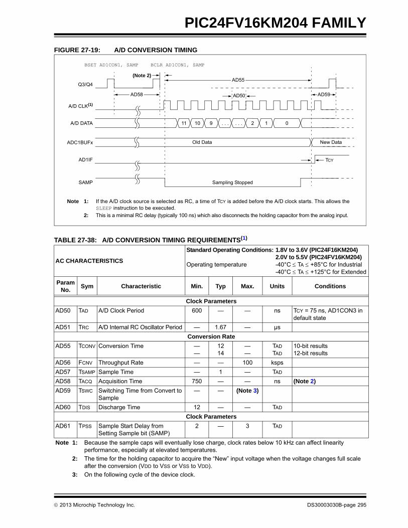
PIC24FV16KM204 FAMILY
FIGURE 27-19: A/D CONVERSION TIMING
TABLE 27-38: A/D CONVERSION TIMING REQUIREMENTS(1)
AC CHARACTERISTICS
Standard Operating Conditions: 1.8V to 3.6V (PIC24F16KM204)2.0V to 5.5V (PIC24FV16KM204)
Operating temperature -40°C TA +85°C for Industrial-40°C TA +125°C for Extended
Param No.
Sym Characteristic Min. Typ Max. Units Conditions
Clock Parameters
AD50 TAD A/D Clock Period 600 — — ns TCY = 75 ns, AD1CON3 in default state
AD51 TRC A/D Internal RC Oscillator Period — 1.67 — µs
Conversion Rate
AD55 TCONV Conversion Time ——
1214
——
TAD
TAD
10-bit results12-bit results
AD56 FCNV Throughput Rate — — 100 ksps
AD57 TSAMP Sample Time — 1 — TAD
AD58 TACQ Acquisition Time 750 — — ns (Note 2)
AD59 TSWC Switching Time from Convert to Sample
— — (Note 3)
AD60 TDIS Discharge Time 12 — — TAD
Clock Parameters
AD61 TPSS Sample Start Delay from Setting Sample bit (SAMP)
2 — 3 TAD
Note 1: Because the sample caps will eventually lose charge, clock rates below 10 kHz can affect linearity performance, especially at elevated temperatures.
2: The time for the holding capacitor to acquire the “New” input voltage when the voltage changes full scale after the conversion (VDD to VSS or VSS to VDD).
3: On the following cycle of the device clock.
AD55
AD50AD58
BCLR AD1CON1, SAMP
Q3/Q4
A/D CLK(1)
A/D DATA
ADC1BUFx
AD1IF
SAMP
Old Data
Sampling Stopped
New Data
(Note 2)
11 10 9 2 1 0
Note 1: If the A/D clock source is selected as RC, a time of TCY is added before the A/D clock starts. This allows the SLEEP instruction to be executed.
2: This is a minimal RC delay (typically 100 ns) which also disconnects the holding capacitor from the analog input.
. . . . . .
TCY
BSET AD1CON1, SAMP
AD59
2013 Microchip Technology Inc. DS30003030B-page 295

PIC24FV16KM204 FAMILY
TABLE 27-39: 8-BIT DIGITAL-TO-ANALOG CONVERTER SPECIFICATIONS
AC CHARACTERISTICS
Standard Operating Conditions: 1.8V to 3.6V (PIC24F16KM204)2.0V to 5.5V (PIC24FV16KM204)
Operating temperature -40°C TA +85°C for Industrial-40°C TA +125°C for Extended
Param No.
Sym Characteristic Min. Typ Max. Units Comments
Resolution 8 — — bits
DACREF<1:0> Input Voltage Range
AVSS + 1.8 — AVDD V
Differential Linearity Error (DNL)
— — ±0.5 LSb
Integral Linearity Error (INL) — — ±1.5 LSb
Offset Error — — ±0.5 LSb
Gain Error — — ±3.0 LSb
Monotonicity — — — — (Note 1)
Output Voltage Range AVSS + 50 AVSS + 5 to AVDD – 5
AVDD – 50 mV 0.5V input overdrive, no output loading
Slew Rate — 5 — V/µs
Settling Time — 10 — µs
Note 1: DAC output voltage never decreases with an increase in the data code.
DS30003030B-page 296 2013 Microchip Technology Inc.

PIC24FV16KM204 FAMILY
28.0 PACKAGING INFORMATION
28.1 Package Marking Information
Legend: XX...X Product-specific informationY Year code (last digit of calendar year)YY Year code (last 2 digits of calendar year)WW Week code (week of January 1 is week ‘01’)NNN Alphanumeric traceability code Pb-free JEDEC designator for Matte Tin (Sn)* This package is Pb-free. The Pb-free JEDEC designator ( )
can be found on the outer packaging for this package.
Note: In the event the full Microchip part number cannot be marked on one line, itwill be carried over to the next line, thus limiting the number of availablecharacters for customer-specific information.
3e
3e
20-Lead PDIP (300 mil)
XXXXXXXXXXXXXXXXXXXXXXXXXXXXXXXXXX
YYWWNNN3e
Example
-I/PPIC24F08KM101
1342M7W
20-Lead SSOP (5.30 mm)
XXXXXXXXXXXXXXXXXXXXXX
YYWWNNN
Example
24F08KM101301-I/SS
1342M7W
3e
20-Lead SOIC (7.50 mm)
XXXXXXXXXXXXXXXXXXXXXXXXXXXXXXXXXXXXXXXXXX
YYWWNNN
Example
PIC24F08KM101-I/SO
1342M7W
3e
XXXXXXX
20-Lead QFN
XXXXXXXYYWWNNN
24F08KM
Example
101/ML1310017
3e
2013 Microchip Technology Inc. DS30003030B-page 297

PIC24FV16KM204 FAMILY
PIN 1
28-Lead SOIC (7.50 mm)
XXXXXXXXXXXXXXXXXXXXXXXXXXXXXXXXXXXXXXXXXXXXXXXXXXXXXXXXXXXX
YYWWNNN
Example
PIC24F16KM202
1342M7W
28-Lead QFN (6x6 mm)
XXXXXXXXXXXXXXXXYYWWNNN
3e-I/SO
Example
F16KM202-I/ML
1342M7W3e
PIN 1
28-Lead SPDIP (.300")
XXXXXXXXXXXXXXXXXXXXXXXXXXXXXXXXXX
YYWWNNN
Example
-I/SPPIC24F16KM202
1342M7W3e
28-Lead SSOP (5.30 mm)
XXXXXXXXXXXXXXXXXXXXXXXX
YYWWNNN
Example
PIC24F16KM102-I/SS
1342M7W
3e
44-Lead TQFP (10x10x1 mm)
XXXXXXXXXXXXXXXXXXXXXXXXXXXXXX
YYWWNNN
24FV16KM204-I/PT1342M7W
3e
Example
DS30003030B-page 298 2013 Microchip Technology Inc.
PIC24FV16KM204 FAMILY
XXXXXXXXXXX
44-Lead QFN (8x8x0.9 mm)
XXXXXXXXXXXXXXXXXXXXXX
YYWWNNN
Example
3e
PIN 1
PIC24FV16KM
Example
204-I/ML1342M7W
PIN 1
XXXXXXXXXXXXXXXXXXXXXXX
YYWWNNN
XXXXXXXX
48-Lead UQFN (6x6x0.5 mm)
XXXXXXXXYYWWNNN
3e
PIN 1
24FV16KM204/MV1342M7W
PIN 1
2013 Microchip Technology Inc. DS30003030B-page 299

PIC24FV16KM204 FAMILY
28.2 Package Details
The following sections give the technical details of the packages.
!"# $% &" ' ()"&'"!&) & #*&& & # +%&,& !&- ' !!#.#&"# '#%!&"!!#%!&"!!!& $ #/ !# ' !#& .0
1,2 1!' ! & $& " !**&"&& !
3& '!&" &4 #*!( ! ! & 4 %&& #&&&255***''54
6&! 7,8.' !9'&! 7 7: ;
7"') %! 7 & 1,& & < < # #4 4 !! - 1! & & < <"# &"# =#& . - - -# #4 =#& . >: 9 & > - ?& & 9 - 9 #4 !! > 6 9 #=#& ) ? 9* 9 #=#& ) > : *+ 1 < < -
N
E1NOTE 1
D
1 2 3
A
A1
A2
L
e
b1
b
E
c
eB
* ,1
DS30003030B-page 300 2013 Microchip Technology Inc.

PIC24FV16KM204 FAMILY
!"# $ %& $
!"# $% &" ' ()"&'"!&) & #*&& & # ' !!#.#&"# '#%!&"!!#%!&"!!!& $ #'' !# - ' !#& .0
1,2 1!' ! & $& " !**&"&& !.32 % ' !("!"*&"&& (%%'&"! !
3& '!&" &4 #*!( ! ! & 4 %&& #&&&255***''54
6&! 99..' !9'&! 7 7: ;
7"') %! 7 & ?1,: 8 & < < # #4 4 !! ? >&#%% < <: =#& . > ># #4 =#& . - ?: 9 & ? 3&9 & 9 3&& 9 .39 #4 !! < 3& @ @ >@9 #=#& ) < ->
φ
LL1
A2c
eb
A1
A
1 2
NOTE 1
E1
E
D
N
* ,1
2013 Microchip Technology Inc. DS30003030B-page 301
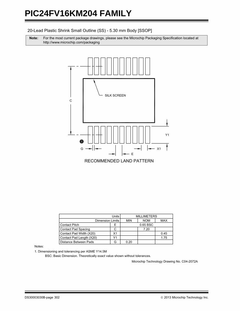
PIC24FV16KM204 FAMILY
Note: For the most current package drawings, please see the Microchip Packaging Specification located at http://www.microchip.com/packaging
DS30003030B-page 302 2013 Microchip Technology Inc.
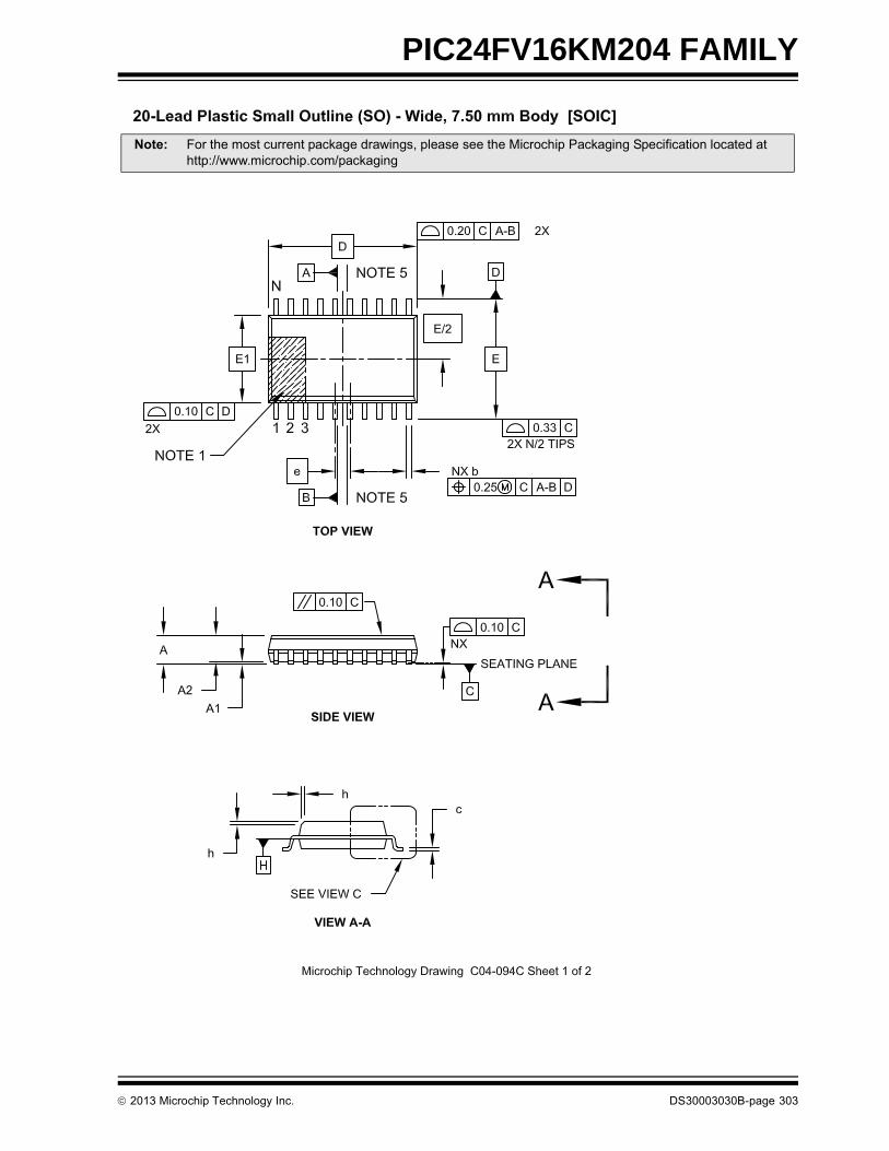
PIC24FV16KM204 FAMILY
Note: For the most current package drawings, please see the Microchip Packaging Specification located at http://www.microchip.com/packaging
2013 Microchip Technology Inc. DS30003030B-page 303
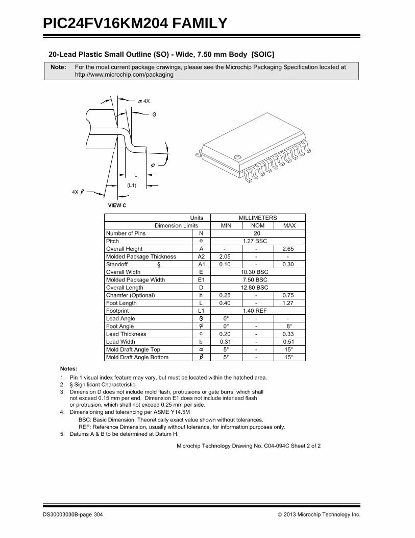
PIC24FV16KM204 FAMILY
Note: For the most current package drawings, please see the Microchip Packaging Specification located at http://www.microchip.com/packaging
DS30003030B-page 304 2013 Microchip Technology Inc.

PIC24FV16KM204 FAMILY
Note: For the most current package drawings, please see the Microchip Packaging Specification located at http://www.microchip.com/packaging
2013 Microchip Technology Inc. DS30003030B-page 305

PIC24FV16KM204 FAMILY
'( )#*+,-,-&.'(
!"# $% &" ' ()"&'"!&) & #*&& & # 4 !!*!"& #- ' !#& .0
1,2 1!' ! & $& " !**&"&& !.32 % ' !("!"*&"&& (%%'&"! !
3& '!&" &4 #*!( ! ! & 4 %&& #&&&255***''54
6&! 99..' !9'&! 7 7: ;
7"') %! 7 & 1,: 8 & > &#%% ,&&4 !! - .3: =#& . 1,.$! ##=#& . ? >: 9 & 1,.$! ##9 & ? >,&&=#& ) > -,&&9 & 9 - ,&&&.$! ## A < <
DEXPOSED
PAD
E
E2
2
1
N
TOP VIEW NOTE 1
N
L
K
b
e
D2
2
1
A
A1A3
BOTTOM VIEW
* ,?1
DS30003030B-page 306 2013 Microchip Technology Inc.

PIC24FV16KM204 FAMILY
3& '!&" &4 #*!( ! ! & 4 %&& #&&&255***''54
2013 Microchip Technology Inc. DS30003030B-page 307

PIC24FV16KM204 FAMILY
/ #
!"# $% &" ' ()"&'"!&) & #*&& & # +%&,& !&- ' !!#.#&"# '#%!&"!!#%!&"!!!& $ #/ !# ' !#& .0
1,2 1!' ! & $& " !**&"&& !
3& '!&" &4 #*!( ! ! & 4 %&& #&&&255***''54
6&! 7,8.' !9'&! 7 7: ;
7"') %! 7 >& 1,& & < < # #4 4 !! - 1! & & < <"# &"# =#& . - --# #4 =#& . > : 9 & - -? & & 9 - 9 #4 !! > 6 9 #=#& ) 9* 9 #=#& ) > : *+ 1 < < -
NOTE 1
N
1 2
D
E1
eB
c
E
L
A2
eb
b1A1
A
3
* ,1
DS30003030B-page 308 2013 Microchip Technology Inc.

PIC24FV16KM204 FAMILY
/ !"# $ %& $
!"# $% &" ' ()"&'"!&) & #*&& & # ' !!#.#&"# '#%!&"!!#%!&"!!!& $ #'' !# - ' !#& .0
1,2 1!' ! & $& " !**&"&& !.32 % ' !("!"*&"&& (%%'&"! !
3& '!&" &4 #*!( ! ! & 4 %&& #&&&255***''54
6&! 99..' !9'&! 7 7: ;
7"') %! 7 >& ?1,: 8 & < < # #4 4 !! ? >&#%% < <: =#& . > ># #4 =#& . - ?: 9 & 3&9 & 9 3&& 9 .39 #4 !! < 3& @ @ >@9 #=#& ) < ->
LL1
cA2
A1
A
EE1
D
N
1 2
NOTE 1b
e
φ
* ,-1
2013 Microchip Technology Inc. DS30003030B-page 309

PIC24FV16KM204 FAMILY
Note: For the most current package drawings, please see the Microchip Packaging Specification located at http://www.microchip.com/packaging
DS30003030B-page 310 2013 Microchip Technology Inc.
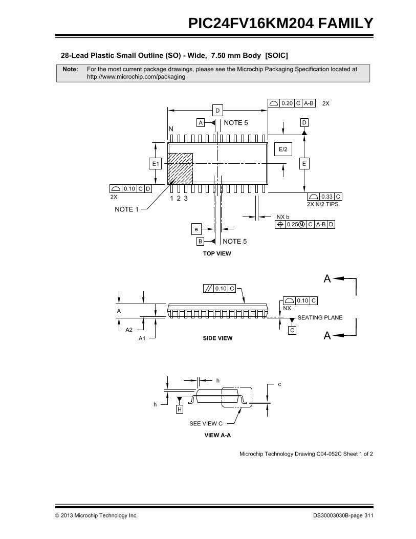
PIC24FV16KM204 FAMILY
Note: For the most current package drawings, please see the Microchip Packaging Specification located at http://www.microchip.com/packaging
2013 Microchip Technology Inc. DS30003030B-page 311
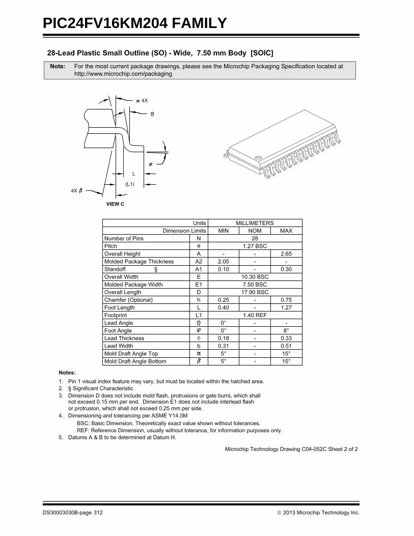
PIC24FV16KM204 FAMILY
Note: For the most current package drawings, please see the Microchip Packaging Specification located at http://www.microchip.com/packaging
DS30003030B-page 312 2013 Microchip Technology Inc.

PIC24FV16KM204 FAMILY
Note: For the most current package drawings, please see the Microchip Packaging Specification located at http://www.microchip.com/packaging
2013 Microchip Technology Inc. DS30003030B-page 313

PIC24FV16KM204 FAMILY
/ '( )#*+0-0'(1 !&%%2 * !
!"# $% &" ' ()"&'"!&) & #*&& & # 4 !!*!"& #- ' !#& .0
1,2 1!' ! & $& " !**&"&& !.32 % ' !("!"*&"&& (%%'&"! !
3& '!&" &4 #*!( ! ! & 4 %&& #&&&255***''54
6&! 99..' !9'&! 7 7: ;
7"') %! 7 >& ?1,: 8 & > &#%% ,&&4 !! - .3: =#& . ?1,.$! ##=#& . -? - : 9 & ?1,.$! ##9 & -? - ,&&=#& ) - - -,&&9 & 9 ,&&&.$! ## A < <
D EXPOSED D2
e
b
K
E2
E
L
N
NOTE 1
1
22
1
N
A
A1A3
TOP VIEW BOTTOM VIEW
PAD
* ,1
DS30003030B-page 314 2013 Microchip Technology Inc.
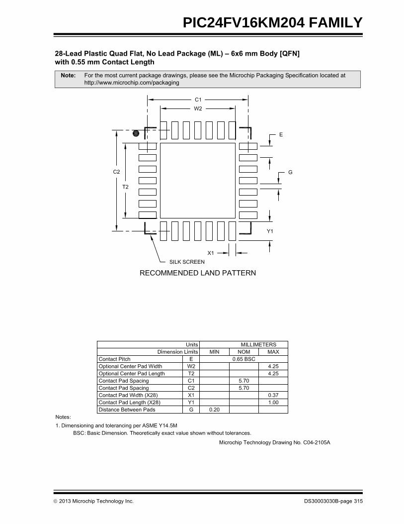
PIC24FV16KM204 FAMILY
/ '( )#*+0-0'(1 !&%%2 * !
3& '!&" &4 #*!( ! ! & 4 %&& #&&&255***''54
2013 Microchip Technology Inc. DS30003030B-page 315

PIC24FV16KM204 FAMILY
,, 3!'( 4#35-5-5)&3'(
!"# $% &" ' ()"&'"!&) & #*&& & # ,'% !& ! &B!C ' - ' !!#.#&"# '#%!&"!!#%!&"!!!& $ #'' !# ' !#& .0
1,2 1!' ! & $& " !**&"&& !.32 % ' !("!"*&"&& (%%'&"! !
3& '!&" &4 #*!( ! ! & 4 %&& #&&&255***''54
6&! 99..' !9'&! 7 7: ;
7"') %9 #! 7 9 #& >1,: 8 & < < # #4 4 !! &#%% < 3&9 & 9 ? 3&& 9 .33& @ -@ @: =#& . 1,: 9 & 1,# #4 =#& . 1,# #4 9 & 1,9 #4 !! < 9 #=#& ) - - #%& @ @ -@#%& 1&&' @ @ -@
A
E
E1
DD1
e
b
NOTE 1NOTE 2
N
1 2 3
c
A1L
A2L1
α
φ
β
* ,?1
DS30003030B-page 316 2013 Microchip Technology Inc.

PIC24FV16KM204 FAMILY
Note: For the most current package drawings, please see the Microchip Packaging Specification located at http://www.microchip.com/packaging
2013 Microchip Technology Inc. DS30003030B-page 317

PIC24FV16KM204 FAMILY
DS30003030B-page 318 2013 Microchip Technology Inc.

PIC24FV16KM204 FAMILY
2013 Microchip Technology Inc. DS30003030B-page 319

PIC24FV16KM204 FAMILY
DS30003030B-page 320 2013 Microchip Technology Inc.

PIC24FV16KM204 FAMILY
Note: For the most current package drawings, please see the Microchip Packaging Specification located at http://www.microchip.com/packaging
2013 Microchip Technology Inc. DS30003030B-page 321

PIC24FV16KM204 FAMILY
Note: For the most current package drawings, please see the Microchip Packaging Specification located at http://www.microchip.com/packaging
DS30003030B-page 322 2013 Microchip Technology Inc.

PIC24FV16KM204 FAMILY
2013 Microchip Technology Inc. DS30003030B-page 323

PIC24FV16KM204 FAMILY
NOTES:
DS30003030B-page 324 2013 Microchip Technology Inc.

PIC24FV16KM204 FAMILY
APPENDIX A: REVISION HISTORY
Revision A (February 2013)
Original data sheet for the PIC24FV16KM204 family ofdevices.
Revision B (July 2013)
Updates all references to PGCx and PGDx pin functionsthroughout the document to PGECx and PGEDx.
Updates Section 4.0 “Memory Organization” tochange bit 12 in the following registers to reserved (“r”designation):
• CCP1CON1L (Table 4-8)
• CCP2CON1L (Table 4-9)
• CCP3CON1L (Table 4-10)
• CCP4CON1L (Table 4-11)
• CCP5CON1L (Table 4-12)
Updates Section 13.0 “Capture/Compare/PWM/Timer Modules (MCCP and SCCP)”:
• Replaces bit 12 of CCPxCON1L (CCPSLP) and its description with a reserved bit
• Removes references to asynchronous operation in Sleep mode (and in other occurrences throughout the document)
• Modifies Section 13.1 “Time Base Generator” to add synchronous operation limitations; adds Table 13-1 to list valid clock options for all operating modes
• Removes the system clock as a time base input option
• Removes external input sources, comparators and CTMU as synchronization sources in Table 13-6; clarifies that other selected sources must be synchronous
Removes the input buffer from the band gap referenceinput in Figure 20-1.
Adds BUFCON0 register description (Register 20-2) toSection 20.0 “8-Bit Digital-to-Analog Converter(DAC)”.
Changes references to internal band gap voltages(VBG, VBG/2 and BGBUF0) in Section 20.0 “8-BitDigital-to-Analog Converter (DAC)” andSection 22.0 “Comparator Module” to BGBUF1.
Adds minimum VDD conditions for VBG specification inTable 27-15 (Internal Voltage Regulator Specifications).
Other minor typographical corrections throughout thedocument.
2013 Microchip Technology Inc. DS30003030B-page 325

PIC24FV16KM204 FAMILY
NOTES:
DS30003030B-page 326 2013 Microchip Technology Inc.

PIC24FV16KM204 FAMILY
INDEX
AA/D
Buffer Data Formats ................................................. 225Control Registers ..................................................... 212
AD1CHITH/L .................................................... 212AD1CHS .......................................................... 212AD1CON1 ........................................................ 212AD1CON2 ........................................................ 212AD1CON3 ........................................................ 212AD1CON5 ........................................................ 212AD1CSSH/L ..................................................... 212AD1CTMENH/L ............................................... 212
Sampling Requirements ........................................... 223Transfer Function ..................................................... 224
AC Characteristics8-Bit DAC Specifications .......................................... 296A/D Conversion Requirements ................................ 295A/D Module Specifications ....................................... 294Capacitive Loading Requirements on
Output Pins ...................................................... 279CLKO and I/O Requirements ................................... 282External Clock Requirements .................................. 280Internal RC Accuracy ............................................... 281Internal RC Oscillator Specifications ........................ 281Load Conditions and Requirements ......................... 279PLL Clock Specification ........................................... 281Reset, Watchdog Timer. Oscillator Start-up Timer,
Power-up Timer, Brown-out Reset Requirements .................................................. 284
Temperature and Voltage Specifications ................. 279Assembler
MPASM Assembler .................................................. 262
BBlock Diagrams
12-Bit A/D Converter ................................................ 21012-Bit A/D Converter Analog Input Model ................ 22316-Bit Timer1 ........................................................... 14132-Bit Timer Mode ................................................... 146Accessing Program Memory with
Table Instructions .............................................. 65CALL Stack Frame ..................................................... 63CLCx Input Source Selection ................................... 197CLCx Logic Function Combinatorial Options ........... 196CLCx Module ........................................................... 195Comparator Voltage Reference ............................... 239Comparator x Module .............................................. 235Conceptual MCCPx/SCCPx Modules ...................... 143CPU Programmer’s Model ......................................... 37CTMU Connections, Internal Configuration for
Capacitance Measurement .............................. 242CTMU Connections, Internal Configuration for
Pulse Delay Generation ................................... 243CTMU Connections, Internal Configuration for
Time Measurement .......................................... 242Data Access from Program Space Address Generation
64Data EEPROM Addressing with TBLPAG and
NVM Registers ................................................... 75Dual 16-Bit Timer Mode ........................................... 145High/Low-Voltage Detect (HLVD) ............................ 207Individual Comparator Configurations ...................... 236Input Capture x Module ............................................ 148
MCLR Pin Connections Example .............................. 30MSSPx (I2C Master Mode) ...................................... 161MSSPx (I2C Mode) .................................................. 161MSSPx (SPI Mode) ................................................. 160On-Chip Voltage Regulator Connections ................ 257Output Compare x Module ...................................... 147PIC24F CPU Core ..................................................... 36PIC24FXXXXX Family (General) ............................... 19PSV Operation ........................................................... 66Recommended Minimum Connections ...................... 29Reset System ............................................................ 79RTCC Module .......................................................... 181Series Resistor ........................................................ 132Shared I/O Port Structure ........................................ 137Simplified Single DACx Module ............................... 229Simplified UARTx .................................................... 173Single Operational Amplifier .................................... 233SPI Master/Slave Connection .................................. 160Suggested Oscillator Circuit Placement .................... 33System Clock ........................................................... 121Table Register Addressing ........................................ 67Timer Clock Generator ............................................ 144Watchdog Timer (WDT) ........................................... 258
Brown-out ResetTrip Points ............................................................... 269
CC Compilers
MPLAB XC Compilers ............................................. 262Capture/Compare/PWM/Timer
Auxiliary Output ....................................................... 149General Purpose Timer ........................................... 145Input Capture Mode ................................................. 148Output Compare Mode ............................................ 147Synchronization Sources ......................................... 153Time Base Generator .............................................. 144
Capture/Compare/PWM/Timer (MCCP, SCCP) .............. 143Charge Time Measurement Unit. See CTMU.CLC
Control Registers ..................................................... 198Code Examples
Assembly Code Sequence for Clock Switching ....... 128C Code Power-Saving Entry .................................... 131C Code Sequence for Clock Switching .................... 128Data EEPROM Bulk Erase ........................................ 77Data EEPROM Unlock Sequence ............................. 73Erasing a Program Memory Row,
Assembly Language .......................................... 70Erasing a Program Memory Row, C Language ......... 70I/O Port Write/Read ................................................. 140Initiating a Programming Sequence,
Assembly Language .......................................... 72Initiating a Programming Sequence, C Language ..... 72Loading the Write Buffers, Assembly Language ....... 71Loading the Write Buffers, C Language .................... 71Reading Data EEPROM Using
TBLRD Command ............................................. 78Setting the RTCWREN Bit in ‘C’ .............................. 182Setting the RTCWREN Bit in Assembly .................. 182Single-Word Erase .................................................... 76Single-Word Write to Data EEPROM ........................ 77Ultra Low-Power Wake-up Initialization ................... 132
Code Protection ............................................................... 259Comparator ...................................................................... 235
2013 Microchip Technology Inc. DS30003030B-page 327
PIC24FV16KM204 FAMILY
Comparator Voltage Reference ....................................... 239Configuring ............................................................... 239
Configurable Logic Cell (CLC) ......................................... 195Configuration Bits ............................................................. 249CPU
ALU ............................................................................ 39Control Registers ....................................................... 38Core Registers ........................................................... 36Programmer’s Model .................................................. 35
CTMUMeasuring Capacitance ........................................... 241Measuring Time ....................................................... 242Pulse Generation and Delay .................................... 243
Customer Change Notification Service ............................ 332Customer Notification Service .......................................... 332Customer Support ............................................................ 332
DData EEPROM Memory ..................................................... 73
Erasing ....................................................................... 76Operations ................................................................. 75Programming
Bulk Erase .......................................................... 77Reading Data EEPROM .................................... 78Single-Word Write .............................................. 77
Programming Control RegistersNVMADR(U) ...................................................... 75NVMCON ........................................................... 73NVMKEY ............................................................ 73
Data MemoryAddress Space ........................................................... 43
Width .................................................................. 43Near Data Space ....................................................... 44Organization, Alignment ............................................. 44SFR Space ................................................................. 44Software Stack ........................................................... 63
Data SpaceMemory Map .............................................................. 43
DC CharacteristicsBOR Trip Points ....................................................... 269Comparator .............................................................. 276CTMU Current Source ............................................. 277Data EEPROM Memory ........................................... 276High/Low-Voltage Detect ......................................... 269I/O Pin Input Specifications ...................................... 274I/O Pin Output Specifications ................................... 275Idle Current (IIDLE) ................................................... 271Internal Voltage Regulator ....................................... 277Operating Current (IDD) ............................................ 270Operational Amplifier ............................................... 278Power-Down Current (IPD) ....................................... 272Program Memory ..................................................... 275Temperature and Voltage Specifications ................. 268
Demo/Development Boards, Evaluation and Starter Kits ............................................................... 264
Development Support ...................................................... 261Third-Party Tools ..................................................... 264
Device FeaturesPIC24F16KM104 Family ............................................ 16PIC24F16KM204 Family ............................................ 15PIC24FV16KM104 Family ......................................... 18PIC24FV16KM204 Family ......................................... 17
Device Overview ................................................................ 13Core Features ............................................................ 13Other Special Features .............................................. 14Pinout Description ...................................................... 20
Dual Operational Amplifier ............................................... 233
EElectrical Characteristics
Absolute Maximum Ratings ..................................... 265Thermal Operating Conditions ................................. 268Thermal Packaging .................................................. 268
EquationsA/D Conversion Clock Period .................................. 223UARTx Baud Rate with BRGH = 0 .......................... 174UARTx Baud Rate with BRGH = 1 .......................... 174
Errata ................................................................................. 11Examples
Baud Rate Error Calculation (BRGH = 0) ................ 174
FFlash Program Memory
Control Registers ....................................................... 68Enhanced ICSP Operation ........................................ 68Programming Algorithm ............................................. 70Programming Operations ........................................... 68RTSP Operation ........................................................ 68Table Instructions ...................................................... 67
GGetting Started Guidelines ................................................. 29
External Oscillator Pins .............................................. 33ICSP Pins .................................................................. 32Master Clear (MCLR) Pin .......................................... 30Power Supply Pins ..................................................... 30Unused I/Os ............................................................... 33Voltage Regulator Pin (VCAP) .................................... 31
HHigh/Low-Voltage Detect (HLVD) .................................... 207
II/O Ports
Analog Port Pins Configuration ................................ 138Analog Selection Registers ...................................... 138Input Change Notification ........................................ 140Open-Drain Configuration ........................................ 138Parallel (PIO) ........................................................... 137
In-Circuit Debugger .......................................................... 259In-Circuit Serial Programming (ICSP) .............................. 259Inter-Integrated Circuit. See I2C.Internet Address .............................................................. 332Interrupts
Alternate Interrupt Vector Table (AIVT) ..................... 85Control and Status Registers ..................................... 88Implemented Vectors ................................................. 87Interrupt Vector Table (IVT) ....................................... 85Reset Sequence ........................................................ 85Setup Procedures .................................................... 119Trap Vectors .............................................................. 87Vector Table .............................................................. 86
DS30003030B-page 328 2013 Microchip Technology Inc.
PIC24FV16KM204 FAMILY
MMaster Synchronous Serial Port (MSSP) ......................... 159Microchip Internet Web Site ............................................. 332MPLAB Assembler, Linker, Librarian ............................... 262MPLAB ICD 3 In-Circuit Debugger .................................. 263MPLAB PM3 Device Programmer ................................... 263MPLAB REAL ICE In-Circuit Emulator System ................ 263MPLAB X Integrated Development
Environment Software .............................................. 261MPLAB X SIM Software Simulator ................................... 263MPLIB Object Librarian .................................................... 262MPLINK Object Linker ..................................................... 262
NNear Data Space ............................................................... 44
OOn-Chip Voltage Regulator .............................................. 257Oscillator Configuration
Clock Switching ........................................................ 127Sequence ......................................................... 127
Configuration Bit Values for Clock Selection ........... 122Control Registers ..................................................... 123CPU Clocking Scheme ............................................ 122Initial Configuration on POR .................................... 122Reference Clock Output ........................................... 128
PPackaging
Details ...................................................................... 300Marking .................................................................... 297
PICkit 3 In-Circuit Debugger/Programmer ....................... 263Power-Saving ................................................................... 135Power-Saving Features ................................................... 131
Clock Frequency, Clock Switching ........................... 131Coincident Interrupts ................................................ 132Instruction-Based Modes ......................................... 131
Idle ................................................................... 132Sleep ................................................................ 131
Retention Regulator (RETREG) ............................... 134Selective Peripheral Control .................................... 135Ultra Low-Power Wake-up (ULPWU) ....................... 132Voltage Regulator-Based ......................................... 134
Retention Sleep Mode ..................................... 134Run Mode ........................................................ 134Sleep Mode ...................................................... 134
Product Identification System .......................................... 334Program and Data Memory
Access Using Table Instructions ................................ 65Program Space Visibility ............................................ 66
Program and Data Memory SpacesInterfacing, Addressing .............................................. 63
Program MemoryAddress Space ........................................................... 41Configuration Word Addresses .................................. 42
Program SpaceMemory Map .............................................................. 41
Program Verification ........................................................ 259
RReal-Time Clock and Calendar (RTCC) ........................... 181Register Maps
A/D ............................................................................. 59ANSEL ....................................................................... 60Band Gap Buffer Control ............................................ 61CLC1-2 ....................................................................... 48
Clock Control ............................................................. 62Comparator ................................................................ 61CPU Core .................................................................. 45CTMU ........................................................................ 60DAC1 ......................................................................... 56DAC2 ......................................................................... 56ICN ............................................................................ 46Interrupt Controller ..................................................... 47MCCP1 ...................................................................... 49MCCP2 ...................................................................... 50MCCP3 ...................................................................... 51MSSP1 (I2C/SPI) ....................................................... 54MSSP2 (I2C/SPI) ....................................................... 54NVM ........................................................................... 62Op Amp 1 .................................................................. 56Op Amp 2 .................................................................. 56Pad Configuration ...................................................... 58PMD ........................................................................... 62PORTA ...................................................................... 57PORTB ...................................................................... 57PORTC ...................................................................... 57Real-Time Clock and Calendar ................................. 60SCCP4 ....................................................................... 52SCCP5 ....................................................................... 53Timer1 ....................................................................... 48UART1 ....................................................................... 55UART2 ....................................................................... 55Ultra Low-Power Wake-up ......................................... 62
RegistersAD1CHITH (A/D Scan Compare Hit,
High Word) ...................................................... 219AD1CHITL (A/D Scan Compare Hit,
Low Word) ....................................................... 220AD1CHS (A/D Sample Select) ................................ 218AD1CON1 (A/D Control 1) ....................................... 213AD1CON2 (A/D Control 2) ....................................... 215AD1CON3 (A/D Control 3) ....................................... 216AD1CON5 (A/D Control 5) ....................................... 217AD1CSSH (A/D Input Scan Select, High Word) ...... 221AD1CSSL (A/D Input Scan Select, Low Word) ....... 221AD1CTMENH (CTMU Enable, High Word) ............. 222AD1CTMENL (CTMU Enable, Low Word) ............... 222ALCFGRPT (Alarm Configuration) .......................... 186ALMINSEC (Alarm Minutes and
Seconds Value) ............................................... 190ALMTHDY (Alarm Month and Day Value) ............... 189ALWDHR (Alarm Weekday and Hours Value) ........ 189AMPxCON (Op Amp x Control) ............................... 234ANSA (PORTA Analog Selection) ........................... 138ANSB (PORTB Analog Selection) ........................... 139ANSC (PORTC Analog Selection) ........................... 139BUFCON0 (Internal Voltage Reference
Control 0) ......................................................... 232CCPxCON1H (CCPx Control 1 High) ...................... 152CCPxCON1L (CCPx Control 1 Low) ....................... 150CCPxCON2H (CCPx Control 2 High) ...................... 155CCPxCON2L (CCPx Control 2 Low) ....................... 154CCPxCON3H (CCPx Control 3 High) ...................... 157CCPxCON3L (CCPx Control 3 Low) ....................... 156CCPxSTATL (CCPx Status) .................................... 158CLCxCONH (CLCx Control High) ............................ 199CLCxCONL (CLCx Control Low) ............................. 198CLCxGLSH (CLCx Gate Logic Input Select High) ... 204CLCxGLSL (CLCx Gate Logic Input Select Low) .... 202CLCxSEL (CLCx Input MUX Select) ....................... 200CLKDIV (Clock Divider) ........................................... 125
2013 Microchip Technology Inc. DS30003030B-page 329

PIC24FV16KM204 FAMILY
CMSTAT (Comparator Status) ................................. 238CMxCON (Comparator x Control) ............................ 237CORCON (CPU Control) ........................................... 39CORCON (CPU Core Control) ................................... 90CTMUCON1H (CTMU Control 1 High) .................... 246CTMUCON1L (CTMU Control 1 Low) ...................... 244CTMUCON2L (CTMU Control 2 Low) ...................... 248CVRCON (Comparator Voltage
Reference Control) ........................................... 240DACxCON (DACx Control) ...................................... 230DEVID (Device ID) ................................................... 255DEVREV (Device Revision) ..................................... 256FBS (Boot Segment Configuration) ......................... 249FGS (General Segment Configuration) .................... 250FICD (In-Circuit Debugger Configuration) ................ 254FOSC (Oscillator Configuration) .............................. 251FOSCSEL (Oscillator Selection Configuration) ........ 250FPOR (Reset Configuration) .................................... 253FWDT (Watchdog Timer Configuration) .................. 252HLVDCON (High/Low-Voltage Detect Control) ........ 208IEC0 (Interrupt Enable Control 0) .............................. 98IEC1 (Interrupt Enable Control 1) .............................. 99IEC2 (Interrupt Enable Control 2) ............................ 100IEC3 (Interrupt Enable Control 3) ............................ 100IEC4 (Interrupt Enable Control 4) ............................ 101IEC5 (Interrupt Enable Control 5) ............................ 102IEC6 (Interrupt Enable Control 6) ............................ 102IFS0 (Interrupt Flag Status 0) .................................... 93IFS1 (Interrupt Flag Status 1) .................................... 94IFS2 (Interrupt Flag Status 2) .................................... 95IFS3 (Interrupt Flag Status 3) .................................... 95IFS4 (Interrupt Flag Status 4) .................................... 96IFS5 (Interrupt Flag Status 5) .................................... 97IFS6 (Interrupt Flag Status 6) .................................... 97INTCON1 (Interrupt Control 1) ................................... 91INTCON2 (Interrupt Control 2) ................................... 92INTTREG (Interrupt Control and Status) .................. 118IPC0 (Interrupt Priority Control 0) ............................ 103IPC1 (Interrupt Priority Control 1) ............................ 104IPC10 (Interrupt Priority Control 10) ........................ 111IPC12 (Interrupt Priority Control 12) ........................ 112IPC15 (Interrupt Priority Control 15) ........................ 113IPC16 (Interrupt Priority Control 16) ........................ 114IPC18 (Interrupt Priority Control 18) ........................ 115IPC19 (Interrupt Priority Control 19) ........................ 116IPC2 (Interrupt Priority Control 2) ............................ 105IPC20 (Interrupt Priority Control 20) ........................ 117IPC24 (Interrupt Priority Control 24) ........................ 117IPC3 (Interrupt Priority Control 3) ............................ 106IPC4 (Interrupt Priority Control 4) ............................ 107IPC5 (Interrupt Priority Control 5) ............................ 108IPC6 (Interrupt Priority Control 6) ............................ 109IPC7 (Interrupt Priority Control 7) ............................ 110MINSEC (RTCC Minutes and Seconds Value) ........ 188MTHDY (RTCC Month and Day Value) ................... 187NVMCON (Flash Memory Control) ............................ 69NVMCON (Nonvolatile Memory Control) ................... 74OSCCON (Oscillator Control) .................................. 123OSCTUN (FRC Oscillator Tune) .............................. 126
PADCFG1 (Pad Configuration Control) ................... 171RCFGCAL (RTCC Calibration
and Configuration) ........................................... 183RCON (Reset Control) ............................................... 80REFOCON (Reference Oscillator Control) .............. 129RTCCSWT (RTCC Control/Sample
Window Timer) ................................................ 191RTCPWC (RTCC Configuration 2) .......................... 185SR (ALU STATUS) .............................................. 38, 89SSPxADD (MSSPx Slave Address/Baud
Rate Generator) ............................................... 170SSPxCON1 (MSSPx Control 1, I2C Mode) .............. 166SSPxCON1 (MSSPx Control 1, SPI Mode) ............. 165SSPxCON2 (MSSPx Control 2, I2C Mode) .............. 167SSPxCON3 (MSSPx Control 3, I2C Mode) .............. 169SSPxCON3 (MSSPx Control 3, SPI Mode) ............. 168SSPxMSK (I2C Slave Address Mask) ...................... 170SSPxSTAT (MSSPx Status, I2C Mode) ................... 163SSPxSTAT (MSSPx Status, SPI Mode) .................. 162T1CON (Timer1 Control) ......................................... 142ULPWCON (ULPWU Control) ................................. 133UxMODE (UARTx Mode) ......................................... 176UxRXREG (UARTx Receive) ................................... 180UxSTA (UARTx Status and Control) ........................ 178UxTXREG (UARTx Transmit) .................................. 180WKDYHR (RTCC Weekday and Hours Value) ........ 188YEAR (RTCC Year Value) ....................................... 187
ResetsBrown-out Reset (BOR) ............................................. 83Clock Source Selection .............................................. 82Delay Times ............................................................... 82Device Times ............................................................. 82Low-Power BOR (LPBOR) ........................................ 83RCON Flag Operation ............................................... 81SFR States ................................................................ 83
Retention Regulator (RETREG) ...................................... 134Revision History ............................................................... 325RTCC
Alarm Configuration ................................................. 192Alarm Mask Settings (figure) ................................... 193ALRMVAL Register Mappings ................................. 189Calibration ............................................................... 192Module Registers ..................................................... 182
Mapping ........................................................... 182Clock Source Selection ........................... 182
Write Lock ........................................................ 182Power Control .......................................................... 193RTCVAL Register Mappings .................................... 187Source Clock ........................................................... 181
SSerial Peripheral Interface. See SPI Mode.SFR Space ........................................................................ 44Software Stack ................................................................... 63SPI Mode
I/O Pin Configuration ............................................... 159
DS30003030B-page 330 2013 Microchip Technology Inc.

PIC24FV16KM204 FAMILY
TTimer1 .............................................................................. 141Timing Diagrams
A/D Conversion ........................................................ 295Brown-out Reset Characteristics ............................. 284Capture/Compare/PWM (MCCPx, SCCPx) ............. 285CLKO and I/O Timing ............................................... 282Example SPI Master Mode (CKE = 0) ..................... 286Example SPI Master Mode (CKE = 1) ..................... 287Example SPI Slave Mode (CKE = 0) ....................... 288Example SPI Slave Mode (CKE = 1) ....................... 289External Clock .......................................................... 280I2C Bus Data ............................................................ 290I2C Bus Start/Stop Bits ............................................. 290MSSPx I2C Bus Data ............................................... 293MSSPx I2C Bus Start/Stop Bits ................................ 292Reset, Watchdog Timer. Oscillator Start-up Timer,
Power-up Timer Characteristics ...................... 283Timing Requirements
Capture/Compare/PWM (MCCPx, SCCPx) ............. 285Comparator .............................................................. 285Comparator Voltage Reference Settling Time ......... 285I2C Bus Data (Slave Mode) ...................................... 291I2C Bus Data Requirements (Master Mode) ............ 293I2C Bus Start/Stop Bits (Master Mode) .................... 292I2C Bus Start/Stop Bits (Slave Mode) ...................... 290SPI Mode (Master Mode, CKE = 0) ......................... 286SPI Mode (Master Mode, CKE = 1) ......................... 287SPI Mode (Slave Mode, CKE = 0) ........................... 288SPI Slave Mode (CKE = 1) ...................................... 289
UUART
Baud Rate Generator (BRG) ................................... 174Break and Sync Transmit Sequence ....................... 175IrDA Support ............................................................ 175Operation of UxCTS and UxRTS Control Pins ........ 175Receiving in 8-Bit or 9-Bit Data Mode ..................... 175Transmitting in 8-Bit Data Mode .............................. 175Transmitting in 9-Bit Data Mode .............................. 175
Universal Asynchronous Receiver Transmitter (UART) ................................................. 173
VVoltage Regulator (VREG) .............................................. 134Voltage-Frequency Graph
(PIC24F16KM204 Extended) .................................. 267Voltage-Frequency Graph
(PIC24F16KM204 Industrial) ................................... 266Voltage-Frequency Graph
(PIC24FV16KM204 Extended) ................................ 267Voltage-Frequency Graph
(PIC24FV16KM204 Industrial) ................................. 266
WWatchdog Timer (WDT) ................................................... 257
Windowed Operation ............................................... 258WWW Address ................................................................ 332WWW, On-Line Support .................................................... 11
2013 Microchip Technology Inc. DS30003030B-page 331
PIC24FV16KM204 FAMILY
NOTES:
DS30003030B-page 332 2013 Microchip Technology Inc.
PIC24FV16KM204 FAMILY
THE MICROCHIP WEB SITE
Microchip provides online support via our WWW site atwww.microchip.com. This web site is used as a meansto make files and information easily available tocustomers. Accessible by using your favorite Internetbrowser, the web site contains the followinginformation:
• Product Support – Data sheets and errata, application notes and sample programs, design resources, user’s guides and hardware support documents, latest software releases and archived software
• General Technical Support – Frequently Asked Questions (FAQ), technical support requests, online discussion groups, Microchip consultant program member listing
• Business of Microchip – Product selector and ordering guides, latest Microchip press releases, listing of seminars and events, listings of Microchip sales offices, distributors and factory representatives
CUSTOMER CHANGE NOTIFICATION SERVICE
Microchip’s customer notification service helps keepcustomers current on Microchip products. Subscriberswill receive e-mail notification whenever there arechanges, updates, revisions or errata related to aspecified product family or development tool of interest.
To register, access the Microchip web site atwww.microchip.com. Under “Support”, click on“Customer Change Notification” and follow theregistration instructions.
CUSTOMER SUPPORT
Users of Microchip products can receive assistancethrough several channels:
• Distributor or Representative
• Local Sales Office
• Field Application Engineer (FAE)
• Technical Support
Customers should contact their distributor,representative or Field Application Engineer (FAE) forsupport. Local sales offices are also available to helpcustomers. A listing of sales offices and locations isincluded in the back of this document.
Technical support is available through the web siteat: http://microchip.com/support
2013 Microchip Technology Inc. DS30003030B-page 333

PIC24FV16KM204 FAMILY
NOTES:
DS30003030B-page 334 2013 Microchip Technology Inc.
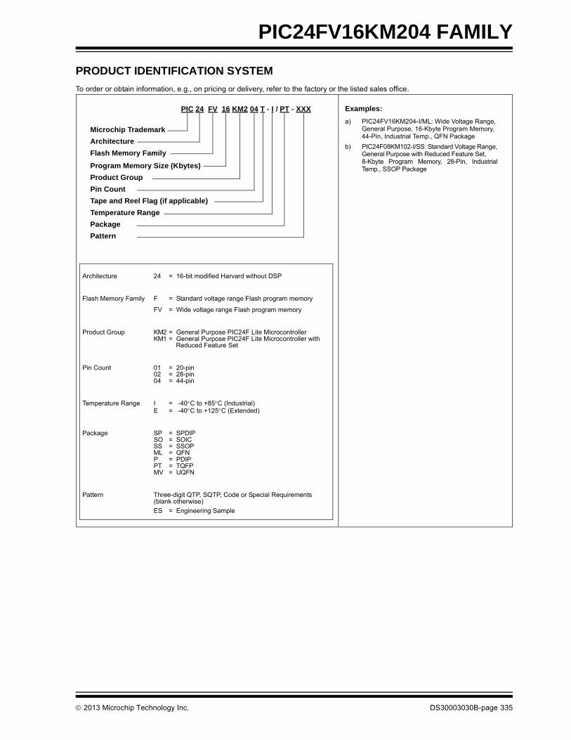
PIC24FV16KM204 FAMILY
PRODUCT IDENTIFICATION SYSTEM
To order or obtain information, e.g., on pricing or delivery, refer to the factory or the listed sales office.
Architecture 24 = 16-bit modified Harvard without DSP
Flash Memory Family F = Standard voltage range Flash program memory
FV = Wide voltage range Flash program memory
Product Group KM2 = General Purpose PIC24F Lite Microcontroller KM1 = General Purpose PIC24F Lite Microcontroller with
Reduced Feature Set
Pin Count 01 = 20-pin02 = 28-pin04 = 44-pin
Temperature Range I = -40C to +85C (Industrial)E = -40C to +125C (Extended)
Package SP = SPDIPSO = SOICSS = SSOPML = QFNP = PDIPPT = TQFPMV = UQFN
Pattern Three-digit QTP, SQTP, Code or Special Requirements (blank otherwise)
ES = Engineering Sample
Examples:
a) PIC24FV16KM204-I/ML: Wide Voltage Range, General Purpose, 16-Kbyte Program Memory, 44-Pin, Industrial Temp., QFN Package
b) PIC24F08KM102-I/SS: Standard Voltage Range,General Purpose with Reduced Feature Set, 8-Kbyte Program Memory, 28-Pin, IndustrialTemp., SSOP Package
Microchip Trademark
Architecture
Flash Memory Family
Program Memory Size (Kbytes)
Product Group
Pin Count
Temperature Range
Package
Pattern
PIC 24 FV 16 KM2 04 T - I / PT - XXX
Tape and Reel Flag (if applicable)
2013 Microchip Technology Inc. DS30003030B-page 335

PIC24FV16KM204 FAMILY
NOTES:
DS30003030B-page 336 2013 Microchip Technology Inc.

Note the following details of the code protection feature on Microchip devices:
• Microchip products meet the specification contained in their particular Microchip Data Sheet.
• Microchip believes that its family of products is one of the most secure families of its kind on the market today, when used in the intended manner and under normal conditions.
• There are dishonest and possibly illegal methods used to breach the code protection feature. All of these methods, to our knowledge, require using the Microchip products in a manner outside the operating specifications contained in Microchip’s Data Sheets. Most likely, the person doing so is engaged in theft of intellectual property.
• Microchip is willing to work with the customer who is concerned about the integrity of their code.
• Neither Microchip nor any other semiconductor manufacturer can guarantee the security of their code. Code protection does not mean that we are guaranteeing the product as “unbreakable.”
Code protection is constantly evolving. We at Microchip are committed to continuously improving the code protection features of ourproducts. Attempts to break Microchip’s code protection feature may be a violation of the Digital Millennium Copyright Act. If such actsallow unauthorized access to your software or other copyrighted work, you may have a right to sue for relief under that Act.
Information contained in this publication regarding deviceapplications and the like is provided only for your convenienceand may be superseded by updates. It is your responsibility toensure that your application meets with your specifications.MICROCHIP MAKES NO REPRESENTATIONS ORWARRANTIES OF ANY KIND WHETHER EXPRESS ORIMPLIED, WRITTEN OR ORAL, STATUTORY OROTHERWISE, RELATED TO THE INFORMATION,INCLUDING BUT NOT LIMITED TO ITS CONDITION,QUALITY, PERFORMANCE, MERCHANTABILITY ORFITNESS FOR PURPOSE. Microchip disclaims all liabilityarising from this information and its use. Use of Microchipdevices in life support and/or safety applications is entirely atthe buyer’s risk, and the buyer agrees to defend, indemnify andhold harmless Microchip from any and all damages, claims,suits, or expenses resulting from such use. No licenses areconveyed, implicitly or otherwise, under any Microchipintellectual property rights.
2013 Microchip Technology Inc.
QUALITY MANAGEMENT SYSTEM CERTIFIED BY DNV
== ISO/TS 16949 ==
Trademarks
The Microchip name and logo, the Microchip logo, dsPIC, FlashFlex, KEELOQ, KEELOQ logo, MPLAB, PIC, PICmicro, PICSTART, PIC32 logo, rfPIC, SST, SST Logo, SuperFlash and UNI/O are registered trademarks of Microchip Technology Incorporated in the U.S.A. and other countries.
FilterLab, Hampshire, HI-TECH C, Linear Active Thermistor, MTP, SEEVAL and The Embedded Control Solutions Company are registered trademarks of Microchip Technology Incorporated in the U.S.A.
Silicon Storage Technology is a registered trademark of Microchip Technology Inc. in other countries.
Analog-for-the-Digital Age, Application Maestro, BodyCom, chipKIT, chipKIT logo, CodeGuard, dsPICDEM, dsPICDEM.net, dsPICworks, dsSPEAK, ECAN, ECONOMONITOR, FanSense, HI-TIDE, In-Circuit Serial Programming, ICSP, Mindi, MiWi, MPASM, MPF, MPLAB Certified logo, MPLIB, MPLINK, mTouch, Omniscient Code Generation, PICC, PICC-18, PICDEM, PICDEM.net, PICkit, PICtail, REAL ICE, rfLAB, Select Mode, SQI, Serial Quad I/O, Total Endurance, TSHARC, UniWinDriver, WiperLock, ZENA and Z-Scale are trademarks of Microchip Technology Incorporated in the U.S.A. and other countries.
SQTP is a service mark of Microchip Technology Incorporated in the U.S.A.
GestIC and ULPP are registered trademarks of Microchip Technology Germany II GmbH & Co. KG, a subsidiary of Microchip Technology Inc., in other countries.
All other trademarks mentioned herein are property of their respective companies.
© 2013, Microchip Technology Incorporated, Printed in the U.S.A., All Rights Reserved.
Printed on recycled paper.
ISBN: 978-1-62077-358-1
Microchip received ISO/TS-16949:2009 certification for its worldwide
DS30003030B-page 337
headquarters, design and wafer fabrication facilities in Chandler and Tempe, Arizona; Gresham, Oregon and design centers in California and India. The Company’s quality system processes and procedures are for its PIC® MCUs and dsPIC® DSCs, KEELOQ® code hopping devices, Serial EEPROMs, microperipherals, nonvolatile memory and analog products. In addition, Microchip’s quality system for the design and manufacture of development systems is ISO 9001:2000 certified.

DS30003030B-page 338 2013 Microchip Technology Inc.
AMERICASCorporate Office2355 West Chandler Blvd.Chandler, AZ 85224-6199Tel: 480-792-7200 Fax: 480-792-7277Technical Support: http://www.microchip.com/supportWeb Address: www.microchip.com
AtlantaDuluth, GA Tel: 678-957-9614 Fax: 678-957-1455
BostonWestborough, MA Tel: 774-760-0087 Fax: 774-760-0088
ChicagoItasca, IL Tel: 630-285-0071 Fax: 630-285-0075
ClevelandIndependence, OH Tel: 216-447-0464 Fax: 216-447-0643
DallasAddison, TX Tel: 972-818-7423 Fax: 972-818-2924
DetroitFarmington Hills, MI Tel: 248-538-2250Fax: 248-538-2260
IndianapolisNoblesville, IN Tel: 317-773-8323Fax: 317-773-5453
Los AngelesMission Viejo, CA Tel: 949-462-9523 Fax: 949-462-9608
Santa ClaraSanta Clara, CA Tel: 408-961-6444Fax: 408-961-6445
TorontoMississauga, Ontario, CanadaTel: 905-673-0699 Fax: 905-673-6509
ASIA/PACIFICAsia Pacific OfficeSuites 3707-14, 37th FloorTower 6, The GatewayHarbour City, KowloonHong KongTel: 852-2401-1200Fax: 852-2401-3431
Australia - SydneyTel: 61-2-9868-6733Fax: 61-2-9868-6755
China - BeijingTel: 86-10-8569-7000 Fax: 86-10-8528-2104
China - ChengduTel: 86-28-8665-5511Fax: 86-28-8665-7889
China - ChongqingTel: 86-23-8980-9588Fax: 86-23-8980-9500
China - HangzhouTel: 86-571-2819-3187 Fax: 86-571-2819-3189
China - Hong Kong SARTel: 852-2943-5100 Fax: 852-2401-3431
China - NanjingTel: 86-25-8473-2460Fax: 86-25-8473-2470
China - QingdaoTel: 86-532-8502-7355Fax: 86-532-8502-7205
China - ShanghaiTel: 86-21-5407-5533 Fax: 86-21-5407-5066
China - ShenyangTel: 86-24-2334-2829Fax: 86-24-2334-2393
China - ShenzhenTel: 86-755-8864-2200 Fax: 86-755-8203-1760
China - WuhanTel: 86-27-5980-5300Fax: 86-27-5980-5118
China - XianTel: 86-29-8833-7252Fax: 86-29-8833-7256
China - XiamenTel: 86-592-2388138 Fax: 86-592-2388130
China - ZhuhaiTel: 86-756-3210040 Fax: 86-756-3210049
ASIA/PACIFICIndia - BangaloreTel: 91-80-3090-4444 Fax: 91-80-3090-4123
India - New DelhiTel: 91-11-4160-8631Fax: 91-11-4160-8632
India - PuneTel: 91-20-2566-1512Fax: 91-20-2566-1513
Japan - OsakaTel: 81-6-6152-7160 Fax: 81-6-6152-9310
Japan - TokyoTel: 81-3-6880- 3770 Fax: 81-3-6880-3771
Korea - DaeguTel: 82-53-744-4301Fax: 82-53-744-4302
Korea - SeoulTel: 82-2-554-7200Fax: 82-2-558-5932 or 82-2-558-5934
Malaysia - Kuala LumpurTel: 60-3-6201-9857Fax: 60-3-6201-9859
Malaysia - PenangTel: 60-4-227-8870Fax: 60-4-227-4068
Philippines - ManilaTel: 63-2-634-9065Fax: 63-2-634-9069
SingaporeTel: 65-6334-8870Fax: 65-6334-8850
Taiwan - Hsin ChuTel: 886-3-5778-366Fax: 886-3-5770-955
Taiwan - KaohsiungTel: 886-7-213-7828Fax: 886-7-330-9305
Taiwan - TaipeiTel: 886-2-2508-8600 Fax: 886-2-2508-0102
Thailand - BangkokTel: 66-2-694-1351Fax: 66-2-694-1350
EUROPEAustria - WelsTel: 43-7242-2244-39Fax: 43-7242-2244-393Denmark - CopenhagenTel: 45-4450-2828 Fax: 45-4485-2829
France - ParisTel: 33-1-69-53-63-20 Fax: 33-1-69-30-90-79
Germany - MunichTel: 49-89-627-144-0 Fax: 49-89-627-144-44
Italy - Milan Tel: 39-0331-742611 Fax: 39-0331-466781
Netherlands - DrunenTel: 31-416-690399 Fax: 31-416-690340
Spain - MadridTel: 34-91-708-08-90Fax: 34-91-708-08-91
UK - WokinghamTel: 44-118-921-5869Fax: 44-118-921-5820
Worldwide Sales and Service
11/29/12