8-Pin, 8-Bit Flash Microcontrollers - Microchip...
96
© 2008 Microchip Technology Inc. DS41319B PIC12F519 Data Sheet 8-Pin, 8-Bit Flash Microcontrollers *8-bit, 8-pin devices protected by Microchip’s Low Pin Count Patent: U.S. Patent No. 5,847,450. Additional U.S. and foreign patents and applications may be issued or pending.
Transcript of 8-Pin, 8-Bit Flash Microcontrollers - Microchip...
© 2008 Microchip Technology Inc. DS41319B
PIC12F519Data Sheet
8-Pin, 8-Bit Flash Microcontrollers
*8-bit, 8-pin devices protected by Microchip’s Low Pin Count Patent: U.S. Patent No. 5,847,450. Additional U.S. andforeign patents and applications may be issued or pending.
Note the following details of the code protection feature on Microchip devices:• Microchip products meet the specification contained in their particular Microchip Data Sheet.
• Microchip believes that its family of products is one of the most secure families of its kind on the market today, when used in the intended manner and under normal conditions.
• There are dishonest and possibly illegal methods used to breach the code protection feature. All of these methods, to our knowledge, require using the Microchip products in a manner outside the operating specifications contained in Microchip’s Data Sheets. Most likely, the person doing so is engaged in theft of intellectual property.
• Microchip is willing to work with the customer who is concerned about the integrity of their code.
• Neither Microchip nor any other semiconductor manufacturer can guarantee the security of their code. Code protection does not mean that we are guaranteeing the product as “unbreakable.”
Code protection is constantly evolving. We at Microchip are committed to continuously improving the code protection features of ourproducts. Attempts to break Microchip’s code protection feature may be a violation of the Digital Millennium Copyright Act. If such actsallow unauthorized access to your software or other copyrighted work, you may have a right to sue for relief under that Act.
Information contained in this publication regarding deviceapplications and the like is provided only for your convenienceand may be superseded by updates. It is your responsibility toensure that your application meets with your specifications.MICROCHIP MAKES NO REPRESENTATIONS ORWARRANTIES OF ANY KIND WHETHER EXPRESS ORIMPLIED, WRITTEN OR ORAL, STATUTORY OROTHERWISE, RELATED TO THE INFORMATION,INCLUDING BUT NOT LIMITED TO ITS CONDITION,QUALITY, PERFORMANCE, MERCHANTABILITY ORFITNESS FOR PURPOSE. Microchip disclaims all liabilityarising from this information and its use. Use of Microchipdevices in life support and/or safety applications is entirely atthe buyer’s risk, and the buyer agrees to defend, indemnify andhold harmless Microchip from any and all damages, claims,suits, or expenses resulting from such use. No licenses areconveyed, implicitly or otherwise, under any Microchipintellectual property rights.
DS41319B-page ii
Trademarks
The Microchip name and logo, the Microchip logo, Accuron, dsPIC, KEELOQ, KEELOQ logo, MPLAB, PIC, PICmicro, PICSTART, rfPIC, SmartShunt and UNI/O are registered trademarks of Microchip Technology Incorporated in the U.S.A. and other countries.
FilterLab, Linear Active Thermistor, MXDEV, MXLAB, SEEVAL, SmartSensor and The Embedded Control Solutions Company are registered trademarks of Microchip Technology Incorporated in the U.S.A.
Analog-for-the-Digital Age, Application Maestro, CodeGuard, dsPICDEM, dsPICDEM.net, dsPICworks, dsSPEAK, ECAN, ECONOMONITOR, FanSense, In-Circuit Serial Programming, ICSP, ICEPIC, Mindi, MiWi, MPASM, MPLAB Certified logo, MPLIB, MPLINK, mTouch, PICkit, PICDEM, PICDEM.net, PICtail, PIC32 logo, PowerCal, PowerInfo, PowerMate, PowerTool, REAL ICE, rfLAB, Select Mode, Total Endurance, WiperLock and ZENA are trademarks of Microchip Technology Incorporated in the U.S.A. and other countries.
SQTP is a service mark of Microchip Technology Incorporated in the U.S.A.
All other trademarks mentioned herein are property of their respective companies.
© 2008, Microchip Technology Incorporated, Printed in the U.S.A., All Rights Reserved.
Printed on recycled paper.
© 2008 Microchip Technology Inc.
Microchip received ISO/TS-16949:2002 certification for its worldwide headquarters, design and wafer fabrication facilities in Chandler and Tempe, Arizona; Gresham, Oregon and design centers in California and India. The Company’s quality system processes and procedures are for its PIC® MCUs and dsPIC® DSCs, KEELOQ® code hopping devices, Serial EEPROMs, microperipherals, nonvolatile memory and analog products. In addition, Microchip’s quality system for the design and manufacture of development systems is ISO 9001:2000 certified.
PIC12F5198-Pin, 8-Bit Flash Microcontroller
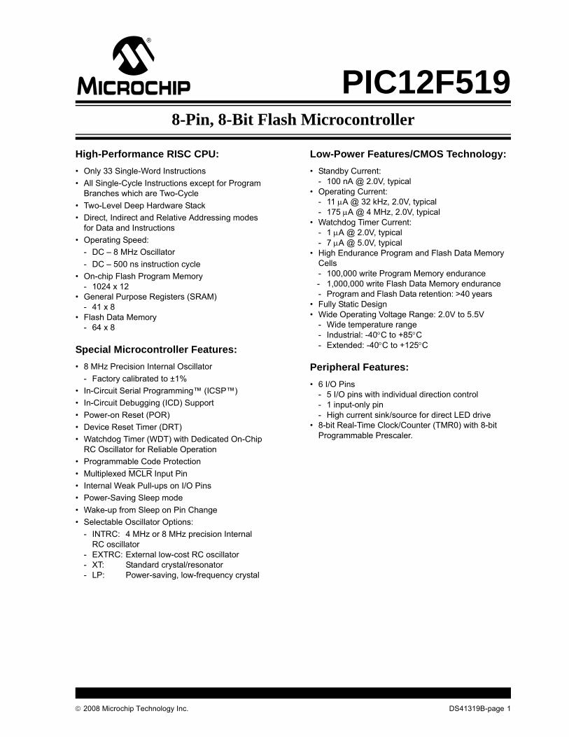
High-Performance RISC CPU: • Only 33 Single-Word Instructions• All Single-Cycle Instructions except for Program
Branches which are Two-Cycle• Two-Level Deep Hardware Stack• Direct, Indirect and Relative Addressing modes
for Data and Instructions• Operating Speed:
- DC – 8 MHz Oscillator- DC – 500 ns instruction cycle
• On-chip Flash Program Memory- 1024 x 12
• General Purpose Registers (SRAM)- 41 x 8
• Flash Data Memory- 64 x 8
Special Microcontroller Features:• 8 MHz Precision Internal Oscillator
- Factory calibrated to ±1%• In-Circuit Serial Programming™ (ICSP™)• In-Circuit Debugging (ICD) Support• Power-on Reset (POR)• Device Reset Timer (DRT)• Watchdog Timer (WDT) with Dedicated On-Chip
RC Oscillator for Reliable Operation• Programmable Code Protection• Multiplexed MCLR Input Pin• Internal Weak Pull-ups on I/O Pins• Power-Saving Sleep mode• Wake-up from Sleep on Pin Change• Selectable Oscillator Options:
- INTRC: 4 MHz or 8 MHz precision Internal RC oscillator
- EXTRC: External low-cost RC oscillator- XT: Standard crystal/resonator- LP: Power-saving, low-frequency crystal
Low-Power Features/CMOS Technology: • Standby Current:
- 100 nA @ 2.0V, typical• Operating Current:
- 11 μA @ 32 kHz, 2.0V, typical- 175 μA @ 4 MHz, 2.0V, typical
• Watchdog Timer Current:- 1 μA @ 2.0V, typical- 7 μA @ 5.0V, typical
• High Endurance Program and Flash Data Memory Cells- 100,000 write Program Memory endurance- 1,000,000 write Flash Data Memory endurance- Program and Flash Data retention: >40 years
• Fully Static Design• Wide Operating Voltage Range: 2.0V to 5.5V
- Wide temperature range - Industrial: -40°C to +85°C- Extended: -40°C to +125°C
Peripheral Features:• 6 I/O Pins
- 5 I/O pins with individual direction control- 1 input-only pin- High current sink/source for direct LED drive
• 8-bit Real-Time Clock/Counter (TMR0) with 8-bit Programmable Prescaler.
© 2008 Microchip Technology Inc. DS41319B-page 1
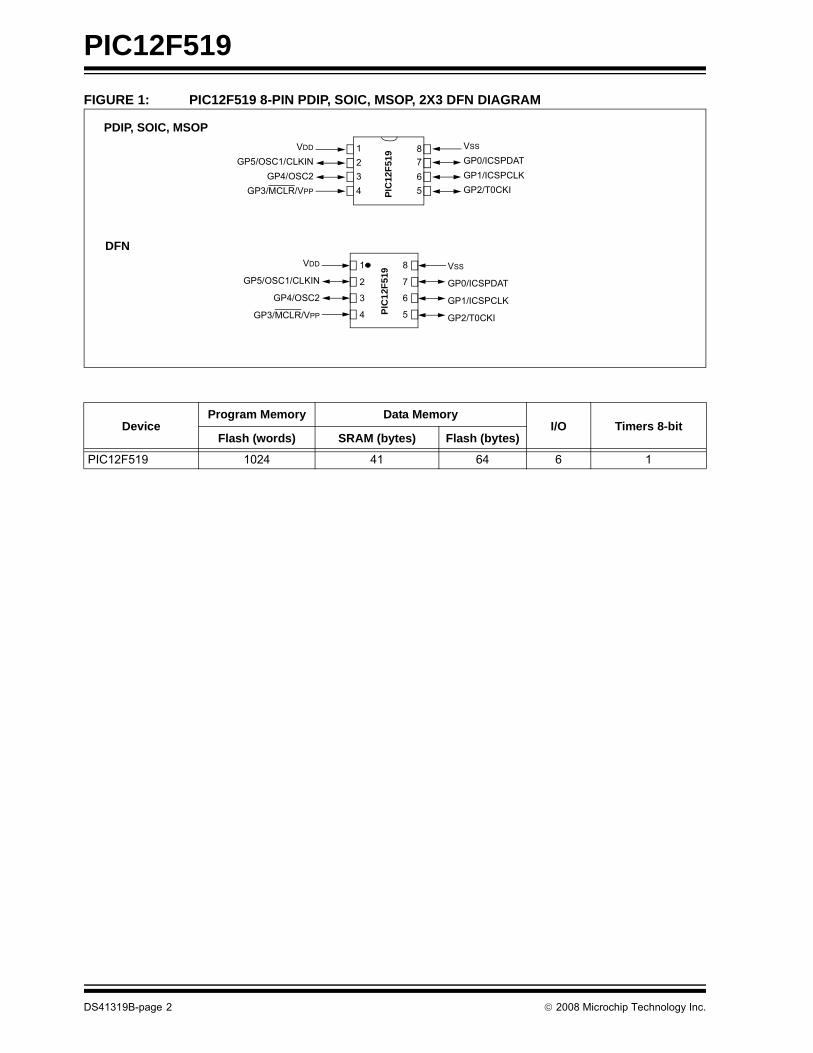
PIC12F519
FIGURE 1: PIC12F519 8-PIN PDIP, SOIC, MSOP, 2X3 DFN DIAGRAMVDD
GP5/OSC1/CLKINGP4/OSC2
GP3/MCLR/VPP
VSS
GP0/ICSPDATGP1/ICSPCLKGP2/T0CKIPI
C12
F519
1234 5
678
DFN
PIC
12F5
19
1
2
3
4
8
7
6
5
VSS
GP0/ICSPDAT
GP1/ICSPCLK
GP2/T0CKI
VDD
GP5/OSC1/CLKIN
GP4/OSC2
GP3/MCLR/VPP
PDIP, SOIC, MSOP
DeviceProgram Memory Data Memory
I/O Timers 8-bitFlash (words) SRAM (bytes) Flash (bytes)
PIC12F519 1024 41 64 6 1
DS41319B-page 2 © 2008 Microchip Technology Inc.
PIC12F519
Table of Contents1.0 General Description .................................................................................................................................................................. 52.0 PIC12F519 Device Varieties .................................................................................................................................................... 73.0 Architectural Overview.............................................................................................................................................................. 94.0 Memory Organization ............................................................................................................................................................. 135.0 Flash Data Memory ................................................................................................................................................................ 216.0 I/O Port ................................................................................................................................................................................... 237.0 Timer0 Module and TMR0 Register ........................................................................................................................................ 318.0 Special Features Of The CPU ................................................................................................................................................ 379.0 Instruction Set Summary ........................................................................................................................................................ 4910.0 Development Support ............................................................................................................................................................. 5711.0 Electrical Characteristics ........................................................................................................................................................ 6112.0 DC and AC Characteristics Graphs and Charts ..................................................................................................................... 7313.0 Packaging Information ............................................................................................................................................................ 83Index ................................................................................................................................................................................................... 89The Microchip Web Site ...................................................................................................................................................................... 91Customer Change Notification Service ............................................................................................................................................... 91Customer Support ............................................................................................................................................................................... 91Reader Response ............................................................................................................................................................................... 92Product Identification System ............................................................................................................................................................. 93TO OUR VALUED CUSTOMERSIt is our intention to provide our valued customers with the best documentation possible to ensure successful use of your Micro-chip products. To this end, we will continue to improve our publications to better suit your needs. Our publications will be refinedand enhanced as new volumes and updates are introduced. If you have any questions or comments regarding this publication, please contact the Marketing Communications Department viaE-mail at [email protected] or fax the Reader Response Form in the back of this data sheet to (480) 792-4150.We welcome your feedback.
Most Current Data SheetTo obtain the most up-to-date version of this data sheet, please register at our Worldwide Web site at:
http://www.microchip.comYou can determine the version of a data sheet by examining its literature number found on the bottom outside corner of any page.The last character of the literature number is the version number, (e.g., DS30000A is version A of document DS30000).
ErrataAn errata sheet, describing minor operational differences from the data sheet and recommended workarounds, may exist for currentdevices. As device/documentation issues become known to us, we will publish an errata sheet. The errata will specify the revisionof silicon and revision of document to which it applies.To determine if an errata sheet exists for a particular device, please check with one of the following:• Microchip’s Worldwide Web site; http://www.microchip.com• Your local Microchip sales office (see last page)• The Microchip Corporate Literature Center; U.S. FAX: (480) 792-7277When contacting a sales office or the literature center, please specify which device, revision of silicon and data sheet (include lit-erature number) you are using.
Customer Notification SystemRegister on our web site at www.microchip.com/cn to receive the most current information on all of our products.
© 2008 Microchip Technology Inc. DS41319B-page 3

PIC12F519
NOTES:DS41319B-page 4 © 2008 Microchip Technology Inc.
PIC12F519
1.0 GENERAL DESCRIPTIONThe PIC12F519 device from Microchip Technology islow-cost, high-performance, 8-bit, fully-static, Flash-based CMOS microcontrollers. They employ a RISCarchitecture with only 33 single-word/single-cycleinstructions. All instructions are single cycle except forprogram branches, which take two cycles. ThePIC12F519 device delivers performance an order ofmagnitude higher than their competitors in the sameprice category. The 12-bit wide instructions are highlysymmetrical, resulting in a typical 2:1 codecompression over other 8-bit microcontrollers in itsclass. The easy-to-use and easy to rememberinstruction set reduces development time significantly.
The PIC12F519 product is equipped with specialfeatures that reduce system cost and powerrequirements. The Power-on Reset (POR) and DeviceReset Timer (DRT) eliminate the need for externalReset circuitry. There are four oscillator configurationsto choose from including INTRC Internal Oscillatormode and the power-saving LP (Low-power) Oscillatormode. Power-Saving Sleep mode, Watchdog Timerand code protection features improve system cost,power and reliability.
The PIC12F519 device is available in the cost-effectiveFlash programmable version, which is suitable forproduction in any volume. The customer can take fulladvantage of Microchip’s price leadership in Flashprogrammable microcontrollers, while benefiting fromthe Flash programmable flexibility.
The PIC12F519 product is supported by a full-featuredmacro assembler, a software simulator, an in-circuitemulator, a low-cost development programmer and afull featured programmer. All the tools are supported onPC and compatible machines.
1.1 ApplicationsThe PIC12F519 device fits in applications ranging frompersonal care appliances and security systems to low-power remote transmitters/receivers. The Flashtechnology makes customizing application programs(transmitter codes, appliance settings, receiverfrequencies, etc.) extremely fast and convenient. Thesmall footprint packages, for through hole or surfacemounting, make these microcontrollers perfect forapplications with space limitations. Low cost, lowpower, high performance, ease of use and I/O flexibilitymake the PIC12F519 device very versatile even inareas where no microcontroller use has beenconsidered before (e.g., timer functions, logic andPLDs in larger systems and coprocessor applications).
TABLE 1-1: FEATURES AND MEMORY OF PIC12F519 PIC12F519
Clock Maximum Frequency of Operation (MHz) 8Memory Flash Program Memory 1024
SRAM Data Memory (bytes) 41Flash Data Memory (bytes) 64
Peripherals Timer Module(s) TMR0Wake-up from Sleep on Pin Change Yes
Features I/O Pins 5Input Pins 1Internal Pull-ups YesIn-Circuit Serial Programming™ YesNumber of Instructions 33Packages 8-pin PDIP, SOIC, MSOP, 2X3 DFN
The PIC12F519 device has Power-on Reset, selectable Watchdog Timer, selectable code-protect, high I/O current capability andprecision internal oscillator.The PIC12F519 device uses serial programming with data pin GP0 and clock pin GP1.
© 2008 Microchip Technology Inc. DS41319B-page 5

PIC12F519
NOTES:DS41319B-page 6 © 2008 Microchip Technology Inc.
PIC12F519
2.0 PIC12F519 DEVICE VARIETIES When placing orders, please use the PIC12F519Product Identification System at the back of this datasheet to specify the correct part number. A variety ofpackaging options are available. Depending onapplication and production requirements, the properdevice option can be selected using the information inthis section.
2.1 Quick Turn Programming (QTP) Devices
Microchip offers a QTP programming service for factoryproduction orders. This service is made available forusers who choose not to program medium-to-highquantity units and whose code patterns have stabilized.The devices are identical to the Flash devices but withall Flash locations and fuse options alreadyprogrammed by the factory. Certain code and prototypeverification procedures do apply before productionshipments are available. Please contact your localMicrochip Technology sales office for more details.
2.2 Serialized Quick Turn ProgrammingSM (SQTPSM) Devices
Microchip offers a unique programming service, where afew user-defined locations in each device areprogrammed with different serial numbers. The serialnumbers may be random, pseudo-random or sequential.
Serial programming allows each device to have aunique number, which can serve as an entry code,password or ID number.
© 2008 Microchip Technology Inc. DS41319B-page 7

PIC12F519
NOTES:DS41319B-page 8 © 2008 Microchip Technology Inc.
PIC12F519
3.0 ARCHITECTURAL OVERVIEW The high performance of the PIC12F519 device canbe attributed to a number of architectural featurescommonly found in RISC microprocessors. To beginwith, the PIC12F519 device uses a Harvard architec-ture in which program and data are accessed on sep-arate buses. This improves bandwidth over traditionalvon Neumann architectures where program and dataare fetched on the same bus. Separating program anddata memory further allows instructions to be sizeddifferently than the 8-bit wide data word. Instructionopcodes are 12 bits wide, making it possible to haveall single-word instructions. A 12-bit wide programmemory access bus fetches a 12-bit instruction in asingle cycle. A two-stage pipeline overlaps fetch andexecution of instructions. Consequently, all instruc-tions (33) execute in a single cycle (500 ns @ 8 MHz,1 μs @ 4 MHz) except for program branches.
Table 3-1 below lists memory supported by thePIC12F519 device.
TABLE 3-1: PIC12F519 MEMORY
The PIC12F519 device can directly or indirectlyaddress its register files and data memory. All SpecialFunction Registers (SFR), including the PC, aremapped in the data memory. The PIC12F519 devicehas a highly orthogonal (symmetrical) instruction setthat makes it possible to carry out any operation, onany register, using any addressing mode. This symmet-rical nature and lack of “special optimal situations”make programming with the PIC12F519 device simple,yet efficient. In addition, the learning curve is reducedsignificantly.
The PIC12F519 device contains an 8-bit ALU andworking register. The ALU is a general purpose arith-metic unit. It performs arithmetic and Boolean functionsbetween data in the working register and any registerfile.
The ALU is 8 bits wide and capable of addition,subtraction, shift and logical operations. Unless other-wise mentioned, arithmetic operations are two’scomplement in nature. In two-operand instructions, oneoperand is typically the W (working) register. The otheroperand is either a file register or an immediateconstant. In single operand instructions, the operand iseither the W register or a file register.
The W register is an 8-bit working register used for ALUoperations. It is not an addressable register.
Depending on the instruction executed, the ALU mayaffect the values of the Carry (C), Digit Carry (DC) andZero (Z) bits in the STATUS register. The C and DC bitsoperate as a borrow and digit borrow out bit, respec-tively, in subtraction. See the SUBWF and ADDWFinstructions for examples.
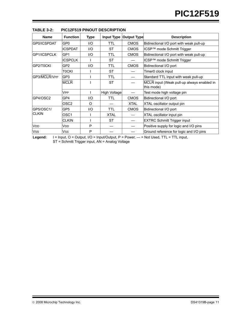
A simplified block diagram is shown in Figure 3-1, withthe corresponding device pins described in Table 3-2.
Device
Program Memory Data Memory
Flash (words)
SRAM (bytes)
Flash Data
(bytes)
PIC12F519 1024 41 64
© 2008 Microchip Technology Inc. DS41319B-page 9
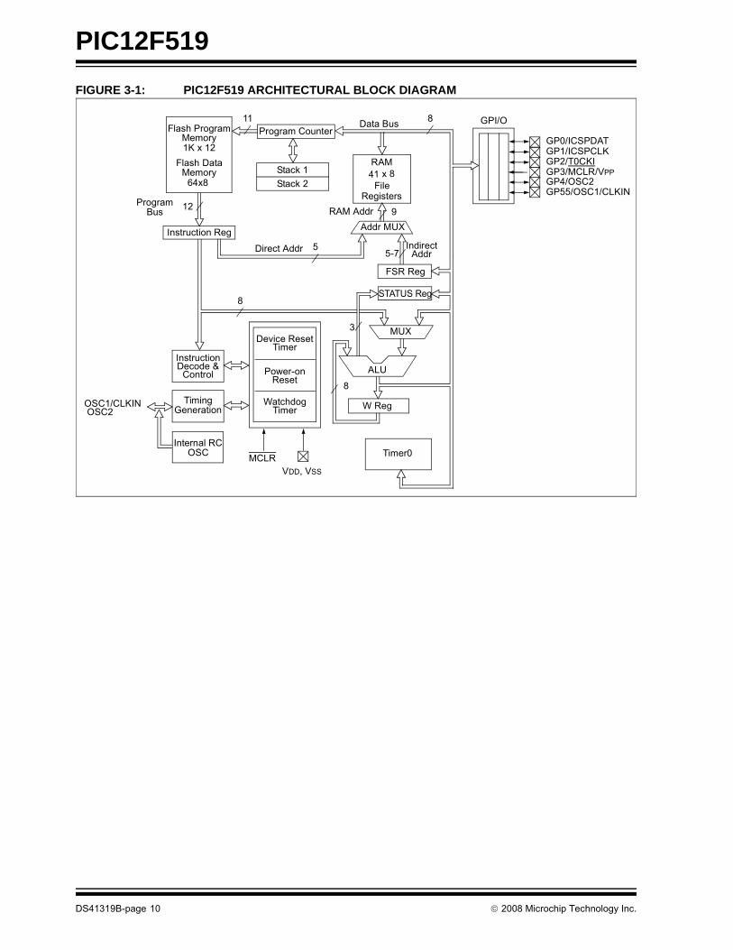
PIC12F519
FIGURE 3-1: PIC12F519 ARCHITECTURAL BLOCK DIAGRAMDevice ResetTimer
Power-onReset
WatchdogTimer
11 Data Bus 8
12ProgramBus
Instruction Reg
Program Counter
RAM
FileRegisters
Direct Addr 5
RAM Addr 9Addr MUX
IndirectAddr
FSR Reg
STATUS Reg
MUX
ALU
W Reg
InstructionDecode &
Control
TimingGeneration
OSC1/CLKINOSC2
MCLRVDD, VSS
Timer0
GPI/O
8
8
GP4/OSC2GP3/MCLR/VPPGP2/T0CKIGP1/ICSPCLKGP0/ICSPDAT
5-7
3
GP55/OSC1/CLKIN
Stack 1Stack 2
41 x 8
Internal RCOSC
Flash ProgramMemory1K x 12
Memory64x8
Flash Data
DS41319B-page 10 © 2008 Microchip Technology Inc.
PIC12F519
TABLE 3-2: PIC12F519 PINOUT DESCRIPTIONName Function Type Input Type Output Type Description
GP0/ICSPDAT GP0 I/O TTL CMOS Bidirectional I/O port with weak pull-upICSPDAT I/O ST CMOS ICSP™ mode Schmitt Trigger
GP1/ICSPCLK GP1 I/O TTL CMOS Bidirectional I/O port with weak pull-upICSPCLK I ST — ICSP™ mode Schmitt Trigger
GP2/T0CKI GP2 I/O TTL CMOS Bidirectional I/O portT0CKI I ST — Timer0 clock input
GP3/MCLR/VPP GP3 I TTL — Standard TTL input with weak pull-upMCLR I ST — MCLR input (Weak pull-up always enabled in
this mode)VPP I High Voltage — Test mode high voltage pin
GP4/OSC2 GP4 I/O TTL CMOS Bidirectional I/O port OSC2 O — XTAL XTAL oscillator output pin
GP5/OSC1/CLKIN
GP5 I/O TTL CMOS Bidirectional I/O port OSC1 I XTAL — XTAL oscillator input pinCLKIN I ST — EXTRC Schmitt Trigger input
VDD VDD P — — Positive supply for logic and I/O pinsVSS VSS P — — Ground reference for logic and I/O pinsLegend: I = Input, O = Output, I/O = Input/Output, P = Power, — = Not Used, TTL = TTL input,
ST = Schmitt Trigger input, AN = Analog Voltage
© 2008 Microchip Technology Inc. DS41319B-page 11
PIC12F519
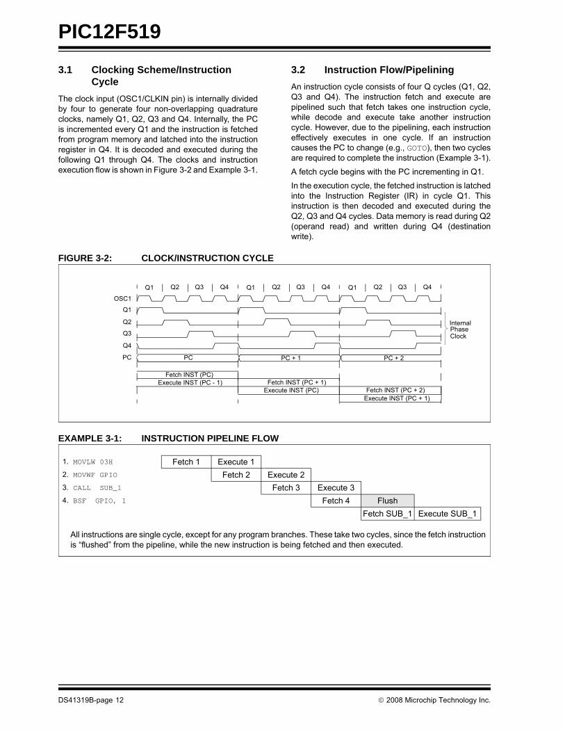
3.1 Clocking Scheme/InstructionCycleThe clock input (OSC1/CLKIN pin) is internally dividedby four to generate four non-overlapping quadratureclocks, namely Q1, Q2, Q3 and Q4. Internally, the PCis incremented every Q1 and the instruction is fetchedfrom program memory and latched into the instructionregister in Q4. It is decoded and executed during thefollowing Q1 through Q4. The clocks and instructionexecution flow is shown in Figure 3-2 and Example 3-1.
3.2 Instruction Flow/PipeliningAn instruction cycle consists of four Q cycles (Q1, Q2,Q3 and Q4). The instruction fetch and execute arepipelined such that fetch takes one instruction cycle,while decode and execute take another instructioncycle. However, due to the pipelining, each instructioneffectively executes in one cycle. If an instructioncauses the PC to change (e.g., GOTO), then two cyclesare required to complete the instruction (Example 3-1).
A fetch cycle begins with the PC incrementing in Q1.
In the execution cycle, the fetched instruction is latchedinto the Instruction Register (IR) in cycle Q1. Thisinstruction is then decoded and executed during theQ2, Q3 and Q4 cycles. Data memory is read during Q2(operand read) and written during Q4 (destinationwrite).
FIGURE 3-2: CLOCK/INSTRUCTION CYCLE
EXAMPLE 3-1: INSTRUCTION PIPELINE FLOW
Q1 Q2 Q3 Q4 Q1 Q2 Q3 Q4 Q1 Q2 Q3 Q4
OSC1
Q1
Q2
Q3
Q4
PC PC PC + 1 PC + 2
Fetch INST (PC)Execute INST (PC - 1) Fetch INST (PC + 1)
Execute INST (PC) Fetch INST (PC + 2)Execute INST (PC + 1)
InternalPhaseClock
All instructions are single cycle, except for any program branches. These take two cycles, since the fetch instructionis “flushed” from the pipeline, while the new instruction is being fetched and then executed.
1. MOVLW 03H Fetch 1 Execute 12. MOVWF GPIO Fetch 2 Execute 23. CALL SUB_1 Fetch 3 Execute 34. BSF GPIO, 1 Fetch 4 Flush
Fetch SUB_1 Execute SUB_1
DS41319B-page 12 © 2008 Microchip Technology Inc.
PIC12F519
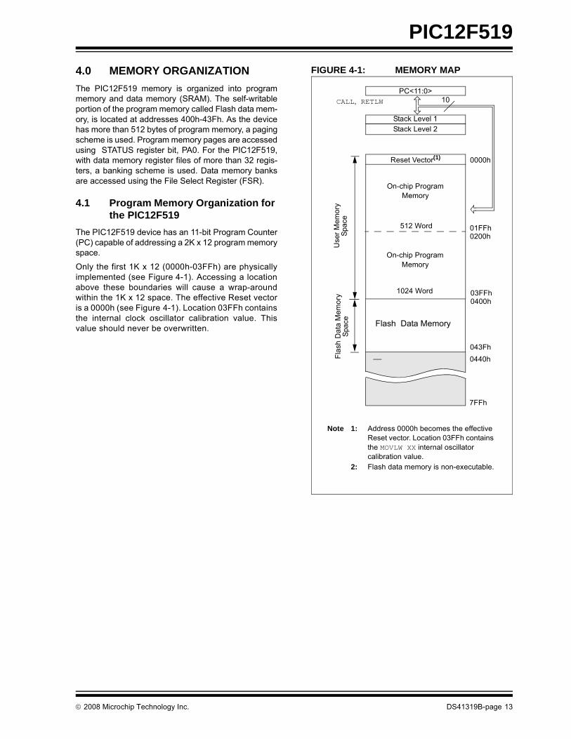
4.0 MEMORY ORGANIZATIONThe PIC12F519 memory is organized into programmemory and data memory (SRAM). The self-writableportion of the program memory called Flash data mem-ory, is located at addresses 400h-43Fh. As the devicehas more than 512 bytes of program memory, a pagingscheme is used. Program memory pages are accessedusing STATUS register bit, PA0. For the PIC12F519,with data memory register files of more than 32 regis-ters, a banking scheme is used. Data memory banksare accessed using the File Select Register (FSR).
4.1 Program Memory Organization for the PIC12F519
The PIC12F519 device has an 11-bit Program Counter(PC) capable of addressing a 2K x 12 program memoryspace.
Only the first 1K x 12 (0000h-03FFh) are physicallyimplemented (see Figure 4-1). Accessing a locationabove these boundaries will cause a wrap-aroundwithin the 1K x 12 space. The effective Reset vectoris a 0000h (see Figure 4-1). Location 03FFh containsthe internal clock oscillator calibration value. Thisvalue should never be overwritten.
FIGURE 4-1: MEMORY MAP
CALL, RETLWPC<11:0>
Stack Level 1Stack Level 2
Use
r Mem
ory
Spac
e
10
0000h
7FFh
01FFh0200h
On-chip ProgramMemory
Reset Vector(1)
Note 1: Address 0000h becomes the effective Reset vector. Location 03FFh contains the MOVLW XX internal oscillator calibration value.
2: Flash data memory is non-executable.
512 Word
1024 Word 03FFh0400h
On-chip ProgramMemory
Flash Data Memory
043Fh0440hFl
ash
Dat
a M
emor
ySp
ace
© 2008 Microchip Technology Inc. DS41319B-page 13
PIC12F519
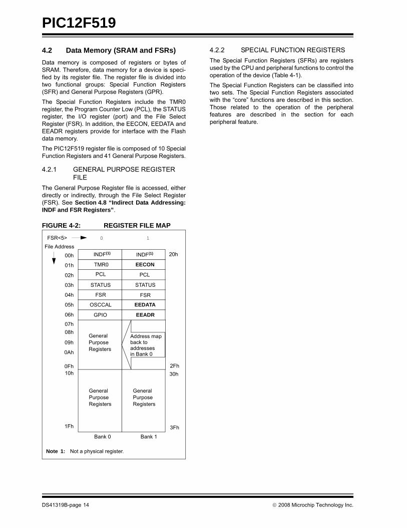
4.2 Data Memory (SRAM and FSRs)Data memory is composed of registers or bytes ofSRAM. Therefore, data memory for a device is speci-fied by its register file. The register file is divided intotwo functional groups: Special Function Registers(SFR) and General Purpose Registers (GPR).The Special Function Registers include the TMR0register, the Program Counter Low (PCL), the STATUSregister, the I/O register (port) and the File SelectRegister (FSR). In addition, the EECON, EEDATA andEEADR registers provide for interface with the Flashdata memory.
The PIC12F519 register file is composed of 10 SpecialFunction Registers and 41 General Purpose Registers.
4.2.1 GENERAL PURPOSE REGISTER FILE
The General Purpose Register file is accessed, eitherdirectly or indirectly, through the File Select Register(FSR). See Section 4.8 “Indirect Data Addressing:INDF and FSR Registers”.
FIGURE 4-2: REGISTER FILE MAP
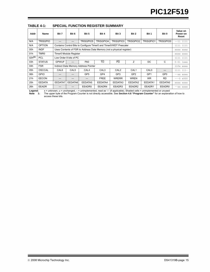
4.2.2 SPECIAL FUNCTION REGISTERSThe Special Function Registers (SFRs) are registersused by the CPU and peripheral functions to control theoperation of the device (Table 4-1).
The Special Function Registers can be classified intotwo sets. The Special Function Registers associatedwith the “core” functions are described in this section.Those related to the operation of the peripheralfeatures are described in the section for eachperipheral feature.
File Address
00h
01h
02h
03h
04h
05h
06h
07h
1Fh
INDF(1)
TMR0
PCL
STATUS
FSR
OSCCAL
GPIO
0Fh10h
Bank 0 Bank 1
3Fh
30h
20h
GeneralPurposeRegisters
GeneralPurposeRegisters
GeneralPurposeRegisters
08h
Note 1: Not a physical register.
FSR<5> 0 1
2Fh
09h
0Ah
INDF(1)
EECON
PCL
STATUS
FSR
EEDATA
EEADR
Address mapback to addressesin Bank 0
DS41319B-page 14 © 2008 Microchip Technology Inc.
PIC12F519
TABLE 4-1: SPECIAL FUNCTION REGISTER SUMMARYAddr Name Bit 7 Bit 6 Bit 5 Bit 4 Bit 3 Bit 2 Bit 1 Bit 0Value on Power-on
Reset
N/A TRISGPIO — — TRISGPIO5 TRISGPIO4 TRISGPIO3 TRISGPIO2 TRISGPIO1 TRISGPIO0 --11 1111
N/A OPTION Contains Control Bits to Configure Timer0 and Timer0/WDT Prescaler 1111 1111
00h INDF Uses Contents of FSR to Address Data Memory (not a physical register) xxxx xxxx
01h TMR0 Timer0 Module Register xxxx xxxx
02h(1) PCL Low Order 8 bits of PC 1111 1111
03h STATUS GPWUF — PA0 TO PD Z DC C 0-01 1xxx
04h FSR Indirect Data Memory Address Pointer 110x xxxx
05h OSCCAL CAL6 CAL5 CAL4 CAL3 CAL2 CAL1 CAL0 — 1111 111-
06h GPIO — — GP5 GP4 GP3 GP2 GP1 GP0 --xx xxxx
21h EECON — — — FREE WRERR WREN WR RD ---0 x000
25h EEDATA EEDATA7 EEDATA6 EEDATA5 EEDATA4 EEDATA3 EEDATA2 EEDATA1 EEDATA0 xxxx xxxx
26h EEADR — — EEADR5 EEADR4 EEADR3 EEADR2 EEADR1 EEADR0 --xx xxxx
Legend: x = unknown, u = unchanged, – = unimplemented, read as ‘0’ (if applicable). Shaded cells = unimplemented or unusedNote 1: The upper byte of the Program Counter is not directly accessible. See Section 4.6 “Program Counter” for an explanation of how to
access these bits.
© 2008 Microchip Technology Inc. DS41319B-page 15
PIC12F519
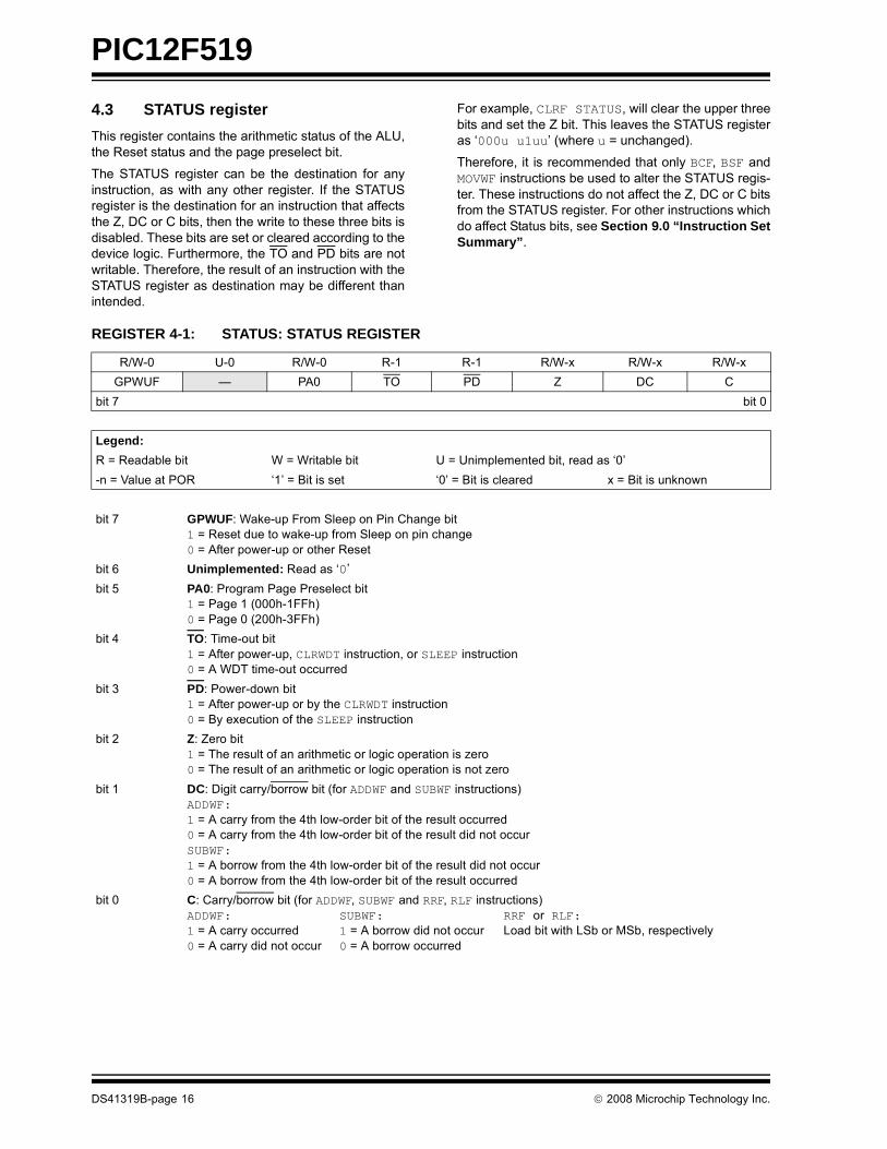
4.3 STATUS registerThis register contains the arithmetic status of the ALU,the Reset status and the page preselect bit.The STATUS register can be the destination for anyinstruction, as with any other register. If the STATUSregister is the destination for an instruction that affectsthe Z, DC or C bits, then the write to these three bits isdisabled. These bits are set or cleared according to thedevice logic. Furthermore, the TO and PD bits are notwritable. Therefore, the result of an instruction with theSTATUS register as destination may be different thanintended.
For example, CLRF STATUS, will clear the upper threebits and set the Z bit. This leaves the STATUS registeras ‘000u u1uu’ (where u = unchanged).
Therefore, it is recommended that only BCF, BSF andMOVWF instructions be used to alter the STATUS regis-ter. These instructions do not affect the Z, DC or C bitsfrom the STATUS register. For other instructions whichdo affect Status bits, see Section 9.0 “Instruction SetSummary”.
REGISTER 4-1: STATUS: STATUS REGISTER
R/W-0 U-0 R/W-0 R-1 R-1 R/W-x R/W-x R/W-xGPWUF — PA0 TO PD Z DC C
bit 7 bit 0
Legend:R = Readable bit W = Writable bit U = Unimplemented bit, read as ‘0’-n = Value at POR ‘1’ = Bit is set ‘0’ = Bit is cleared x = Bit is unknown
bit 7 GPWUF: Wake-up From Sleep on Pin Change bit1 = Reset due to wake-up from Sleep on pin change0 = After power-up or other Reset
bit 6 Unimplemented: Read as ‘0’bit 5 PA0: Program Page Preselect bit
1 = Page 1 (000h-1FFh)0 = Page 0 (200h-3FFh)
bit 4 TO: Time-out bit1 = After power-up, CLRWDT instruction, or SLEEP instruction0 = A WDT time-out occurred
bit 3 PD: Power-down bit1 = After power-up or by the CLRWDT instruction0 = By execution of the SLEEP instruction
bit 2 Z: Zero bit1 = The result of an arithmetic or logic operation is zero0 = The result of an arithmetic or logic operation is not zero
bit 1 DC: Digit carry/borrow bit (for ADDWF and SUBWF instructions)ADDWF:1 = A carry from the 4th low-order bit of the result occurred0 = A carry from the 4th low-order bit of the result did not occurSUBWF:1 = A borrow from the 4th low-order bit of the result did not occur0 = A borrow from the 4th low-order bit of the result occurred
bit 0 C: Carry/borrow bit (for ADDWF, SUBWF and RRF, RLF instructions)ADDWF: SUBWF: RRF or RLF:1 = A carry occurred 1 = A borrow did not occur Load bit with LSb or MSb, respectively0 = A carry did not occur 0 = A borrow occurred
DS41319B-page 16 © 2008 Microchip Technology Inc.
PIC12F519
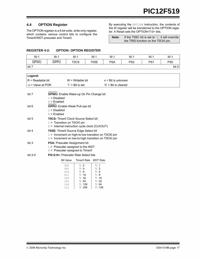
4.4 OPTION RegisterThe OPTION register is a 8-bit wide, write-only register,which contains various control bits to configure theTimer0/WDT prescaler and Timer0.By executing the OPTION instruction, the contents ofthe W register will be transferred to the OPTION regis-ter. A Reset sets the OPTION<7:0> bits.
Note: If the T0SC bit is set to ‘1’, it will overridethe TRIS function on the T0CKI pin.
REGISTER 4-2: OPTION: OPTION REGISTER
W-1 W-1 W-1 W-1 W-1 W-1 W-1 W-1
GPWU GPPU T0CS T0SE PSA PS2 PS1 PS0bit 7 bit 0
Legend:R = Readable bit W = Writable bit x = Bit is unknown-n = Value at POR ‘1’ = Bit is set ‘0’ = Bit is cleared
bit 7 GPWU: Enable Wake-up On Pin Change bit1 = Disabled0 = Enabled
bit 6 GPPU: Enable Weak Pull-ups bit1 = Disabled0 = Enabled
bit 5 T0CS: Timer0 Clock Source Select bit1 = Transition on T0CKI pin0 = Internal instruction cycle clock (CLKOUT)
bit 4 T0SE: Timer0 Source Edge Select bit1 = Increment on high-to-low transition on T0CKI pin0 = Increment on low-to-high transition on T0CKI pin
bit 3 PSA: Prescaler Assignment bit1 = Prescaler assigned to the WDT0 = Prescaler assigned to Timer0
bit 2-0 PS<2:0>: Prescaler Rate Select bits
000001010011100101110111
1 : 21 : 41 : 81 : 161 : 321 : 641 : 1281 : 256
1 : 11 : 21 : 41 : 81 : 161 : 321 : 641 : 128
Bit Value Timer0 Rate WDT Rate
© 2008 Microchip Technology Inc. DS41319B-page 17
PIC12F519
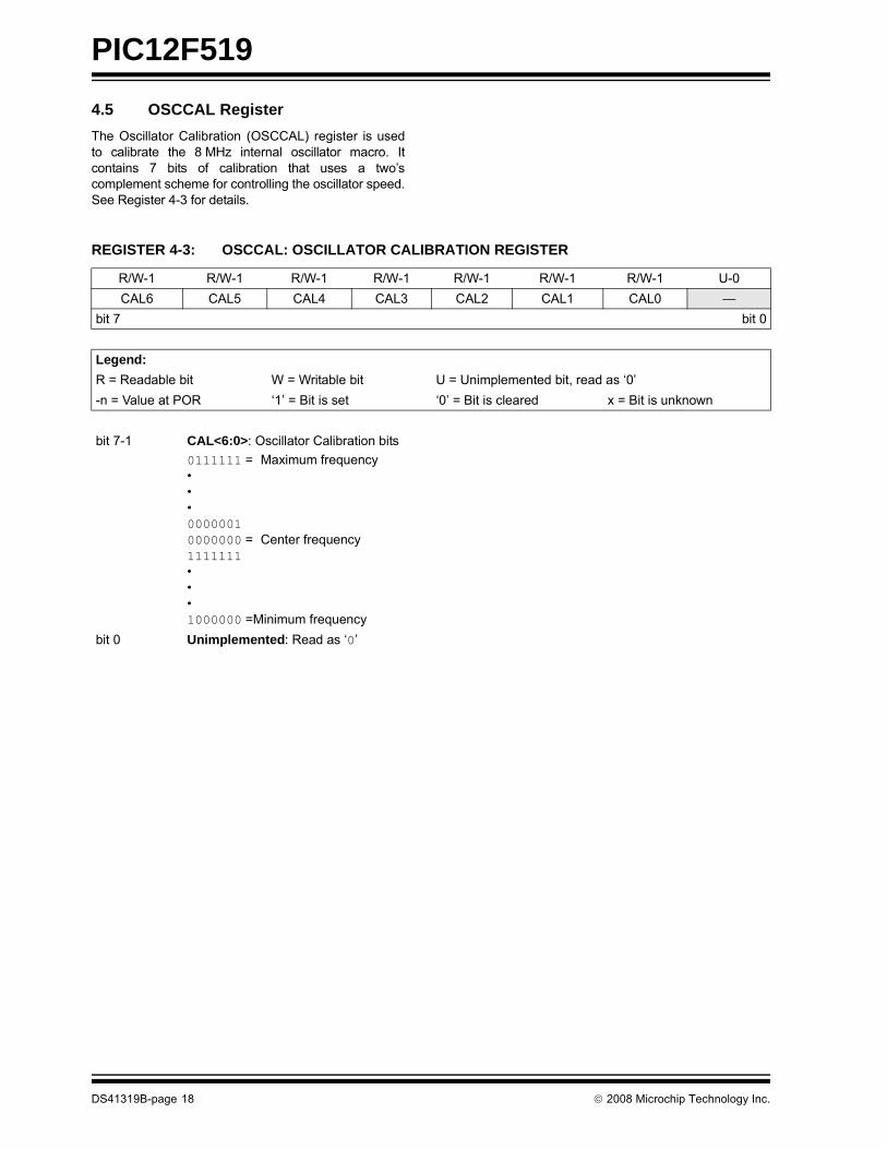
4.5 OSCCAL RegisterThe Oscillator Calibration (OSCCAL) register is usedto calibrate the 8 MHz internal oscillator macro. Itcontains 7 bits of calibration that uses a two’scomplement scheme for controlling the oscillator speed.See Register 4-3 for details.REGISTER 4-3: OSCCAL: OSCILLATOR CALIBRATION REGISTER
R/W-1 R/W-1 R/W-1 R/W-1 R/W-1 R/W-1 R/W-1 U-0CAL6 CAL5 CAL4 CAL3 CAL2 CAL1 CAL0 —
bit 7 bit 0
Legend:R = Readable bit W = Writable bit U = Unimplemented bit, read as ‘0’-n = Value at POR ‘1’ = Bit is set ‘0’ = Bit is cleared x = Bit is unknown
bit 7-1 CAL<6:0>: Oscillator Calibration bits0111111 = Maximum frequency•••0000001 0000000 = Center frequency1111111•••1000000 =Minimum frequency
bit 0 Unimplemented: Read as ‘0’
DS41319B-page 18 © 2008 Microchip Technology Inc.
PIC12F519
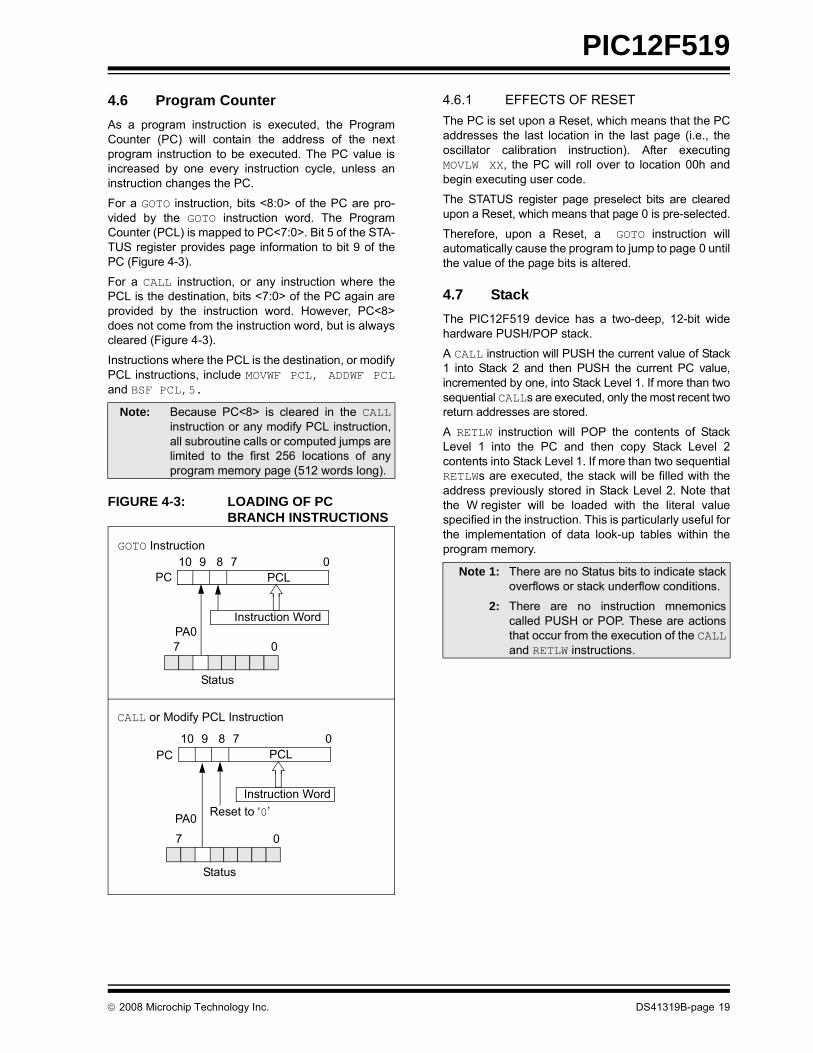
4.6 Program Counter As a program instruction is executed, the ProgramCounter (PC) will contain the address of the nextprogram instruction to be executed. The PC value isincreased by one every instruction cycle, unless aninstruction changes the PC.For a GOTO instruction, bits <8:0> of the PC are pro-vided by the GOTO instruction word. The ProgramCounter (PCL) is mapped to PC<7:0>. Bit 5 of the STA-TUS register provides page information to bit 9 of thePC (Figure 4-3).
For a CALL instruction, or any instruction where thePCL is the destination, bits <7:0> of the PC again areprovided by the instruction word. However, PC<8>does not come from the instruction word, but is alwayscleared (Figure 4-3).
Instructions where the PCL is the destination, or modifyPCL instructions, include MOVWF PCL, ADDWF PCLand BSF PCL,5.
FIGURE 4-3: LOADING OF PCBRANCH INSTRUCTIONS
4.6.1 EFFECTS OF RESETThe PC is set upon a Reset, which means that the PCaddresses the last location in the last page (i.e., theoscillator calibration instruction). After executingMOVLW XX, the PC will roll over to location 00h andbegin executing user code.
The STATUS register page preselect bits are clearedupon a Reset, which means that page 0 is pre-selected.
Therefore, upon a Reset, a GOTO instruction willautomatically cause the program to jump to page 0 untilthe value of the page bits is altered.
4.7 StackThe PIC12F519 device has a two-deep, 12-bit widehardware PUSH/POP stack.
A CALL instruction will PUSH the current value of Stack1 into Stack 2 and then PUSH the current PC value,incremented by one, into Stack Level 1. If more than twosequential CALLs are executed, only the most recent tworeturn addresses are stored.
A RETLW instruction will POP the contents of StackLevel 1 into the PC and then copy Stack Level 2contents into Stack Level 1. If more than two sequentialRETLWs are executed, the stack will be filled with theaddress previously stored in Stack Level 2. Note thatthe W register will be loaded with the literal valuespecified in the instruction. This is particularly useful forthe implementation of data look-up tables within theprogram memory.
Note: Because PC<8> is cleared in the CALLinstruction or any modify PCL instruction,all subroutine calls or computed jumps arelimited to the first 256 locations of anyprogram memory page (512 words long).
PA0
Status
PC8 7 0
PCL910
Instruction Word
7 0
GOTO Instruction
CALL or Modify PCL Instruction
PA0
Status
PC8 7 0
PCL910
Instruction Word
7 0
Reset to ‘0’
Note 1: There are no Status bits to indicate stackoverflows or stack underflow conditions.
2: There are no instruction mnemonicscalled PUSH or POP. These are actionsthat occur from the execution of the CALLand RETLW instructions.
© 2008 Microchip Technology Inc. DS41319B-page 19
PIC12F519
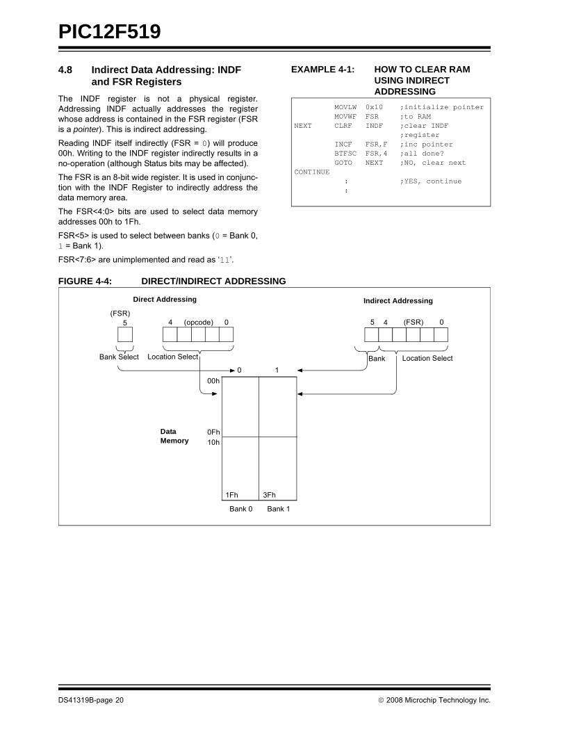
4.8 Indirect Data Addressing: INDFand FSR RegistersThe INDF register is not a physical register.Addressing INDF actually addresses the registerwhose address is contained in the FSR register (FSRis a pointer). This is indirect addressing.
Reading INDF itself indirectly (FSR = 0) will produce00h. Writing to the INDF register indirectly results in ano-operation (although Status bits may be affected).
The FSR is an 8-bit wide register. It is used in conjunc-tion with the INDF Register to indirectly address thedata memory area.
The FSR<4:0> bits are used to select data memoryaddresses 00h to 1Fh.
FSR<5> is used to select between banks (0 = Bank 0,1 = Bank 1).
FSR<7:6> are unimplemented and read as ‘11’.
EXAMPLE 4-1: HOW TO CLEAR RAM USING INDIRECT ADDRESSING
FIGURE 4-4: DIRECT/INDIRECT ADDRESSING
MOVLW 0x10 ;initialize pointerMOVWF FSR ;to RAM
NEXT CLRF INDF ;clear INDF ;register
INCF FSR,F ;inc pointerBTFSC FSR,4 ;all done?GOTO NEXT ;NO, clear next
CONTINUE: ;YES, continue:
Bank Location SelectLocation SelectBank Select
Indirect AddressingDirect Addressing
Data Memory
0Fh10h
Bank 0 Bank 1
045 (FSR)
0 100h
1Fh 3Fh
(opcode) 045(FSR)
DS41319B-page 20 © 2008 Microchip Technology Inc.
PIC12F519
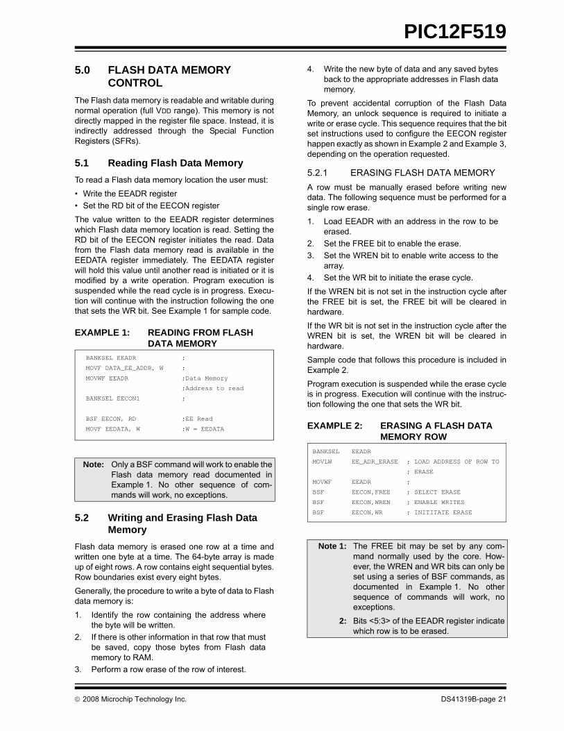
5.0 FLASH DATA MEMORY CONTROL
The Flash data memory is readable and writable duringnormal operation (full VDD range). This memory is notdirectly mapped in the register file space. Instead, it isindirectly addressed through the Special FunctionRegisters (SFRs).
5.1 Reading Flash Data MemoryTo read a Flash data memory location the user must:
• Write the EEADR register• Set the RD bit of the EECON register
The value written to the EEADR register determineswhich Flash data memory location is read. Setting theRD bit of the EECON register initiates the read. Datafrom the Flash data memory read is available in theEEDATA register immediately. The EEDATA registerwill hold this value until another read is initiated or it ismodified by a write operation. Program execution issuspended while the read cycle is in progress. Execu-tion will continue with the instruction following the onethat sets the WR bit. See Example 1 for sample code.
EXAMPLE 1: READING FROM FLASH DATA MEMORY
5.2 Writing and Erasing Flash Data Memory
Flash data memory is erased one row at a time andwritten one byte at a time. The 64-byte array is madeup of eight rows. A row contains eight sequential bytes.Row boundaries exist every eight bytes.
Generally, the procedure to write a byte of data to Flashdata memory is:
1. Identify the row containing the address wherethe byte will be written.
2. If there is other information in that row that mustbe saved, copy those bytes from Flash datamemory to RAM.
3. Perform a row erase of the row of interest.
4. Write the new byte of data and any saved bytesback to the appropriate addresses in Flash datamemory.
To prevent accidental corruption of the Flash DataMemory, an unlock sequence is required to initiate awrite or erase cycle. This sequence requires that the bitset instructions used to configure the EECON registerhappen exactly as shown in Example 2 and Example 3,depending on the operation requested.
5.2.1 ERASING FLASH DATA MEMORYA row must be manually erased before writing newdata. The following sequence must be performed for asingle row erase.
1. Load EEADR with an address in the row to beerased.
2. Set the FREE bit to enable the erase.3. Set the WREN bit to enable write access to the
array.4. Set the WR bit to initiate the erase cycle.
If the WREN bit is not set in the instruction cycle afterthe FREE bit is set, the FREE bit will be cleared inhardware.
If the WR bit is not set in the instruction cycle after theWREN bit is set, the WREN bit will be cleared inhardware.
Sample code that follows this procedure is included inExample 2.
Program execution is suspended while the erase cycleis in progress. Execution will continue with the instruc-tion following the one that sets the WR bit.
EXAMPLE 2: ERASING A FLASH DATA MEMORY ROW
Note: Only a BSF command will work to enable theFlash data memory read documented inExample 1. No other sequence of com-mands will work, no exceptions.
BANKSEL EEADR ;
MOVF DATA_EE_ADDR, W ;
MOVWF EEADR ;Data Memory
;Address to read
BANKSEL EECON1 ;
BSF EECON, RD ;EE Read
MOVF EEDATA, W ;W = EEDATA
Note 1: The FREE bit may be set by any com-mand normally used by the core. How-ever, the WREN and WR bits can only beset using a series of BSF commands, asdocumented in Example 1. No othersequence of commands will work, noexceptions.
2: Bits <5:3> of the EEADR register indicatewhich row is to be erased.
BANKSEL EEADR
MOVLW EE_ADR_ERASE ; LOAD ADDRESS OF ROW TO
; ERASE
MOVWF EEADR ;
BSF EECON,FREE ; SELECT ERASE
BSF EECON,WREN ; ENABLE WRITES
BSF EECON,WR ; INITITATE ERASE
© 2008 Microchip Technology Inc. DS41319B-page 21
PIC12F519
5.2.2 WRITING TO FLASH DATAMEMORYOnce a cell is erased, new data can be written. Pro-gram execution is suspended during the write cycle.The following sequence must be performed for a singlebyte write.
1. Load EEADR with the address.2. Load EEDATA with the data to write.3. Set the WREN bit to enable write access to the
array.4. Set the WR bit to initiate the erase cycle.
If the WR bit is not set in the instruction cycle after theWREN bit is set, the WREN bit will be cleared inhardware.
Sample code that follows this procedure is included inExample 3.
EXAMPLE 3: WRITING A FLASH DATA MEMORY ROW
5.3 Write VerifyDepending on the application, good programmingpractice may dictate that data written to the Flash datamemory be verified. Example 4 is an example of a writeverify.
EXAMPLE 4: WRITE VERIFY OF DATA EEPROM
5.4 Code ProtectionCode protection does not prevent the CPU from per-forming read or write operations on the Flash datamemory. Refer to the code protection chapter for moreinformation.
Note 1: Only a series of BSF commands will workto enable the memory write sequencedocumented in Example 2. No othersequence of commands will work, noexceptions.
2: For reads, erases and writes to the Flashdata memory, there is no need to insert aNOP into the user code as is done onmid-range devices. The instruction imme-diately following the “BSFEECON,WR/RD” will be fetched andexecuted properly.
BANKSEL EEADR
MOVLW EE_ADR_WRITE ; LOAD ADDRESSMOVWF EEADR ;
MOVLW EE_DATA_TO_WRITE ; LOAD DATAMOVWF EEDATA ; INTO EEDATA REGISTERBSF EECON,WREN ; ENABLE WRITES
BSF EECON,WR ; INITITATE ERASE
MOVF EEDATA, W ;EEDATA has not changed
;from previous write
BSF EECON, RD ;Read the value written
XORWF EEDATA, W ;
BTFSS STATUS, Z ;Is data the same
GOTO WRITE_ERR ;No, handle error
;Yes, continue
DS41319B-page 22 © 2008 Microchip Technology Inc.
PIC12F519
6.0 I/O PORTAs with any other register, the I/O register(s) can bewritten and read under program control. However, readinstructions (e.g., MOVF PORTB,W) always read the I/Opins independent of the pin’s Input/Output modes. OnReset, all I/O ports are defined as input (inputs are athigh-impedance) since the I/O control registers are allset.
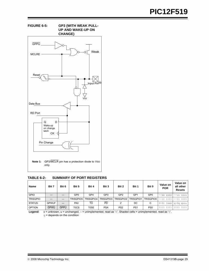
6.1 GPIOGPIO is an 8-bit I/O register. Only the low-order 6 bitsare used (GP<5:0>). Bits 7 and 6 are unimplementedand read as ‘0’s. Please note that GP3 is an input-onlypin. The Configuration Word can set several I/O’s toalternate functions. When acting as alternate functions,the pins will read as ‘0’ during a port read. Pins GP0,GP1, and GP3 can be configured with weak pull-upsand also for wake-up on change. The wake-up onchange and weak pull-up functions are not pin select-able. If GP3/MCLR is configured as MCLR, weak pull-up is always on and wake-up on change for this pin isnot enabled.
6.2 TRIS RegistersThe Output Driver Control registers are loaded withthe contents of the W Register by executing the TRISf instruction. A ‘1’ from a TRISGPIO Register bit putsthe corresponding output driver in a high-impedance(Input) mode. A ‘0’ puts the contents of the output datalatch on the selected pins, enabling the output buffer.
The TRISGPIO register is “write-only”. Bits <5:0> areset (output drivers disabled) upon Reset.
TABLE 6-1: WEAK PULL-UP ENABLED PINS
Note: If the T0CS bit is set to ‘1’, it will overridethe TRISGPIO function on the T0CKI pin.
Pin WPU WU
GP0 Y YGP1 Y YGP2 N NGP3 Y(1) YGP4 N NGP5 N NGP6 N N
Note 1: When MCLRE = 1, the weak pull-up on GP3/MCLR is always enabled.
2: WPU = Weak pull-up; WU = Wake-up.
© 2008 Microchip Technology Inc. DS41319B-page 23
PIC12F519
REGISTER 6-1: GPIO: GPIO REGISTER
U-0 U-0 R/W-x R/W-x R/W-x R/W-x R/W-x R/W-x
— — GP5 GP4 GP3 GP2 GP1 GP0bit 7 bit 0
Legend:R = Readable bit W = Writable bit U = Unimplemented bit, read as ‘0’-n = Value at POR ‘1’ = Bit is set ‘0’ = Bit is cleared x = Bit is unknown
bit 7-6 Unimplemented: Read as ‘0’bit 5-0 GP<5:0>: GPIO I/O Pin bits
1 = GPIO pin is >VIH min.0 = GPIO pin is <VIL max.
REGISTER 6-2: TRISGPIO: TRI-STATE GPIO REGISTER
U-0 U-0 W-1 W-1 W-1 W-1 W-1 W-1
— — TRISGPIO5 TRISGPIO4 TRISGPIO3 TRISGPIO2 TRISGPIO1 TRISGPIO0bit 7 bit 0
Legend:R = Readable bit W = Writable bit U = Unimplemented bit, read as ‘0’-n = Value at POR ‘1’ = Bit is set ‘0’ = Bit is cleared x = Bit is unknown
bit 7-6 Unimplemented: Read as ‘0’bit 5-0 TRISGPIO<5:0>: GPIO Tri-State Control bits
1 = GPIO pin configured as an input (tri-stated)0 = GPIO pin configured as an output
DS41319B-page 24 © 2008 Microchip Technology Inc.
PIC12F519
6.3 I/O InterfacingThe equivalent circuit for an I/O port pin is shown inFigure 6-1. All port pins, except GP3 which is inputonly, may be used for both input and output operations.For input operations, these ports are non-latching. Anyinput must be present until read by an input instruction(e.g., MOVF GPIO, W). The outputs are latched andremain unchanged until the output latch is rewritten. Touse a port pin as output, the corresponding directioncontrol bit in TRISGPIO must be cleared (= 0). For useas an input, the corresponding TRISGPIO bit must beset. Any I/O pin (except GP3) can be programmedindividually as input or output.FIGURE 6-1: PIC12F519 EQUIVALENT CIRCUIT FOR I/O PINS – GP0/GP1
VDD VDD
I/OPin
VSS
Pin Change
Q D
Wake-upon changeLatch
QD
Q
QD
CK Q
Data Latch
TRIS Latch
RD Port
TRIS ‘F’
WREG
WR
Data
GPPU
CK
CK
GP0/ICSPDAT GP1/ICSPCLK
• General purpose I/O • General purpose I/O• In-Circuit Serial Programming™ data • In-circuit Serial Programming™ clock• Wake-up on input change trigger • Wake-up on input change trigger
© 2008 Microchip Technology Inc. DS41319B-page 25
PIC12F519
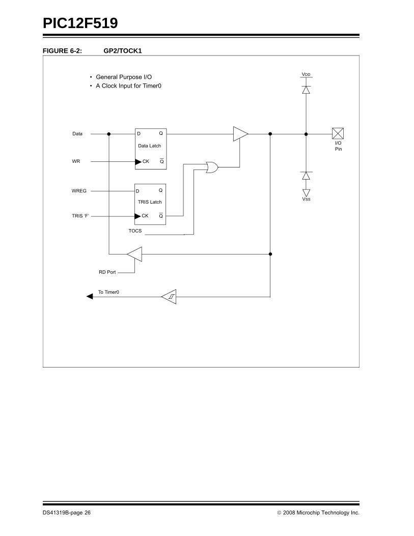
FIGURE 6-2: GP2/TOCK1VDD
I/OPin
VSS
QD
Q
QD
CK Q
Data Latch
TRIS Latch
RD Port
TRIS ‘F’
WREG
WR
Data
CK
To Timer0
TOCS
• General Purpose I/O• A Clock Input for Timer0
DS41319B-page 26 © 2008 Microchip Technology Inc.
PIC12F519
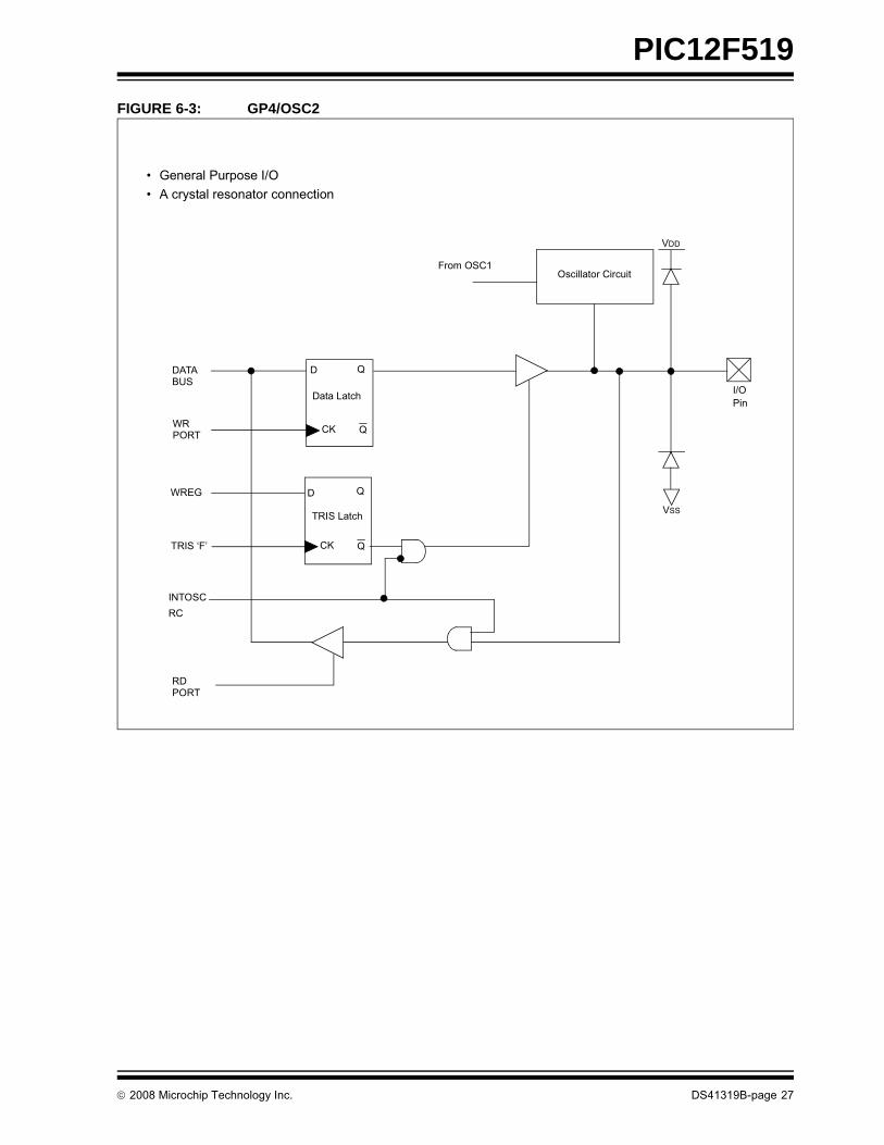
FIGURE 6-3: GP4/OSC2VDD
I/OPin
VSS
QD
Q
QD
CK Q
Data Latch
TRIS Latch
RDPORT
TRIS ‘F’
WREG
WRPORT
DATABUS
CK
INTOSCRC
From OSC1Oscillator Circuit
• General Purpose I/O• A crystal resonator connection
© 2008 Microchip Technology Inc. DS41319B-page 27
PIC12F519
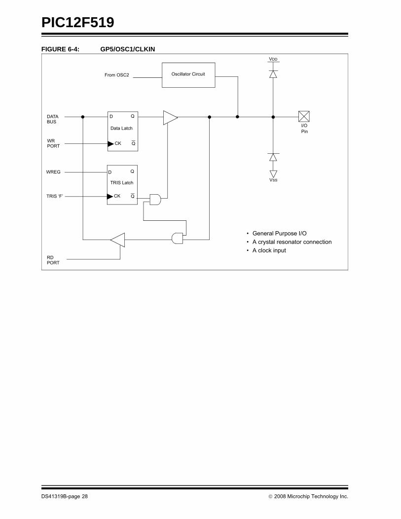
FIGURE 6-4: GP5/OSC1/CLKINVDD
I/OPin
VSS
QD
Q
QD
CK Q
Data Latch
TRIS Latch
RDPORT
TRIS ‘F’
WREG
WRPORT
DATABUS
CK
From OSC2 Oscillator Circuit
• General Purpose I/O• A crystal resonator connection• A clock input
DS41319B-page 28 © 2008 Microchip Technology Inc.
PIC12F519
FIGURE 6-5: GP3 (WITH WEAK PULL-UP AND WAKE-UP ON CHANGE)
TABLE 6-2: SUMMARY OF PORT REGISTERS
Data Bus
RD Port
Note 1: GP3/MCLR pin has a protection diode to VSSonly.
GPPU
D
CK
Q
Pin Change
MCLRE
Reset
Input Pin(1)
Weak
VSS
Wake-upon changelatch
Name Bit 7 Bit 6 Bit 5 Bit 4 Bit 3 Bit 2 Bit 1 Bit 0 Value on POR
Value on all other Resets
GPIO — — GP5 GP4 GP3 GP2 GP1 GP0 --xx xxxx --uu uuuu
TRISGPIO — — TRISGPIO5 TRISGPIO4 TRISGPIO3 TRISGPIO2 TRISGPIO1 TRISGPIO0 --11 1111 --11 1111
STATUS GPWUF — PA0 TO PD Z DC C 0-01 1xxx q-0q quuu
OPTION GPWU GPPU T0CS T0SE PSA PS2 PS1 PS0 1111 1111 1111 1111
Legend: x = unknown, u = unchanged, – = unimplemented, read as ‘0’, Shaded cells = unimplemented, read as ‘0’, q = depends on the condition
© 2008 Microchip Technology Inc. DS41319B-page 29
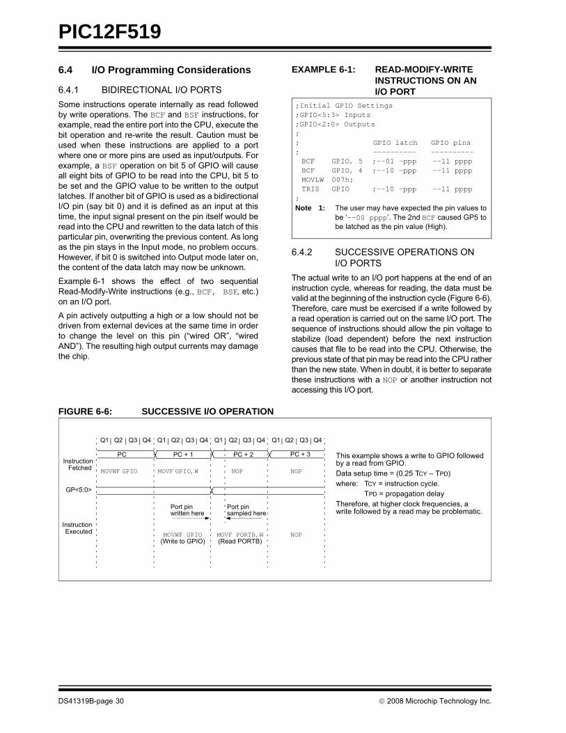
PIC12F519
6.4 I/O Programming Considerations6.4.1 BIDIRECTIONAL I/O PORTSSome instructions operate internally as read followedby write operations. The BCF and BSF instructions, forexample, read the entire port into the CPU, execute thebit operation and re-write the result. Caution must beused when these instructions are applied to a portwhere one or more pins are used as input/outputs. Forexample, a BSF operation on bit 5 of GPIO will causeall eight bits of GPIO to be read into the CPU, bit 5 tobe set and the GPIO value to be written to the outputlatches. If another bit of GPIO is used as a bidirectionalI/O pin (say bit 0) and it is defined as an input at thistime, the input signal present on the pin itself would beread into the CPU and rewritten to the data latch of thisparticular pin, overwriting the previous content. As longas the pin stays in the Input mode, no problem occurs.However, if bit 0 is switched into Output mode later on,the content of the data latch may now be unknown.
Example 6-1 shows the effect of two sequentialRead-Modify-Write instructions (e.g., BCF, BSF, etc.)on an I/O port.
A pin actively outputting a high or a low should not bedriven from external devices at the same time in orderto change the level on this pin (“wired OR”, “wiredAND”). The resulting high output currents may damagethe chip.
EXAMPLE 6-1: READ-MODIFY-WRITE INSTRUCTIONS ON AN I/O PORT
6.4.2 SUCCESSIVE OPERATIONS ONI/O PORTS
The actual write to an I/O port happens at the end of aninstruction cycle, whereas for reading, the data must bevalid at the beginning of the instruction cycle (Figure 6-6).Therefore, care must be exercised if a write followed bya read operation is carried out on the same I/O port. Thesequence of instructions should allow the pin voltage tostabilize (load dependent) before the next instructioncauses that file to be read into the CPU. Otherwise, theprevious state of that pin may be read into the CPU ratherthan the new state. When in doubt, it is better to separatethese instructions with a NOP or another instruction notaccessing this I/O port.
FIGURE 6-6: SUCCESSIVE I/O OPERATION
;Initial GPIO Settings;GPIO<5:3> Inputs;GPIO<2:0> Outputs;; GPIO latch GPIO pins; ---------- ----------BCF GPIO, 5 ;--01 -ppp --11 ppppBCF GPIO, 4 ;--10 -ppp --11 ppppMOVLW 007h;TRIS GPIO ;--10 -ppp --11 pppp
;Note 1: The user may have expected the pin values to
be ‘--00 pppp’. The 2nd BCF caused GP5 to be latched as the pin value (High).
PC PC + 1 PC + 2 PC + 3
Q1 Q2 Q3 Q4 Q1 Q2 Q3 Q4 Q1 Q2 Q3 Q4 Q1 Q2 Q3 Q4
InstructionFetched
GP<5:0>
MOVWF GPIO NOP
Port pinsampled here
NOPMOVF GPIO, W
InstructionExecuted MOVWF GPIO
(Write to GPIO)NOPMOVF PORTB,W
This example shows a write to GPIO followedby a read from GPIO.Data setup time = (0.25 TCY – TPD)where: TCY = instruction cycle.
TPD = propagation delayTherefore, at higher clock frequencies, awrite followed by a read may be problematic.
(Read PORTB)
Port pinwritten here
DS41319B-page 30 © 2008 Microchip Technology Inc.
PIC12F519
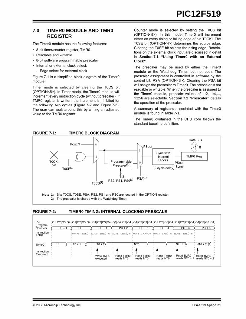
7.0 TIMER0 MODULE AND TMR0 REGISTER
The Timer0 module has the following features:
• 8-bit timer/counter register, TMR0• Readable and writable• 8-bit software programmable prescaler• Internal or external clock select:
- Edge select for external clock
Figure 7-1 is a simplified block diagram of the Timer0module.
Timer mode is selected by clearing the T0CS bit(OPTION<5>). In Timer mode, the Timer0 module willincrement every instruction cycle (without prescaler). IfTMR0 register is written, the increment is inhibited forthe following two cycles (Figure 7-2 and Figure 7-3).The user can work around this by writing an adjustedvalue to the TMR0 register.
Counter mode is selected by setting the T0CS bit(OPTION<5>). In this mode, Timer0 will incrementeither on every rising or falling edge of pin T0CKI. TheT0SE bit (OPTION<4>) determines the source edge.Clearing the T0SE bit selects the rising edge. Restric-tions on the external clock input are discussed in detailin Section 7.1 “Using Timer0 with an ExternalClock”.
The prescaler may be used by either the Timer0module or the Watchdog Timer, but not both. Theprescaler assignment is controlled in software by thecontrol bit, PSA (OPTION<3>). Clearing the PSA bitwill assign the prescaler to Timer0. The prescaler is notreadable or writable. When the prescaler is assigned tothe Timer0 module, prescale values of 1:2, 1:4,...,1:256 are selectable. Section 7.2 “Prescaler” detailsthe operation of the prescaler.
A summary of registers associated with the Timer0module is found in Table 7-1.
The Timer0 contained in the CPU core follows thestandard baseline definition.
FIGURE 7-1: TIMER0 BLOCK DIAGRAM
FIGURE 7-2: TIMER0 TIMING: INTERNAL CLOCK/NO PRESCALE
Note 1: Bits T0CS, T0SE, PSA, PS2, PS1 and PS0 are located in the OPTION register.2: The prescaler is shared with the Watchdog Timer.
T0CKI
T0SE(1)
0
1
1
0pin
T0CS(1)
FOSC/4
ProgrammablePrescaler(2)
Sync withInternalClocks
TMR0 Reg
PSout(2 cycle delay)
PSout
Data Bus
8
PSA(1)PS2, PS1, PS0(1)
3
Sync
PC – 1
Q1 Q2 Q3 Q4 Q1 Q2 Q3 Q4 Q1 Q2 Q3 Q4 Q1 Q2 Q3 Q4 Q1 Q2 Q3 Q4 Q1 Q2 Q3 Q4 Q1 Q2 Q3 Q4 Q1 Q2 Q3 Q4
InstructionFetch
Timer0
PC PC + 1 PC + 2 PC + 3 PC + 4 PC + 6
T0 T0 + 1 T0 + 2 NT0 NT0 + 1 NT0 + 2
MOVWF TMR0 MOVF TMR0,W MOVF TMR0,W MOVF TMR0,W MOVF TMR0,W MOVF TMR0,W
Write TMR0executed
Read TMR0reads NT0
Read TMR0reads NT0
Read TMR0reads NT0
Read TMR0reads NT0 + 1
Read TMR0reads NT0 + 2
InstructionExecuted
PC + 5
PC(ProgramCounter)
© 2008 Microchip Technology Inc. DS41319B-page 31
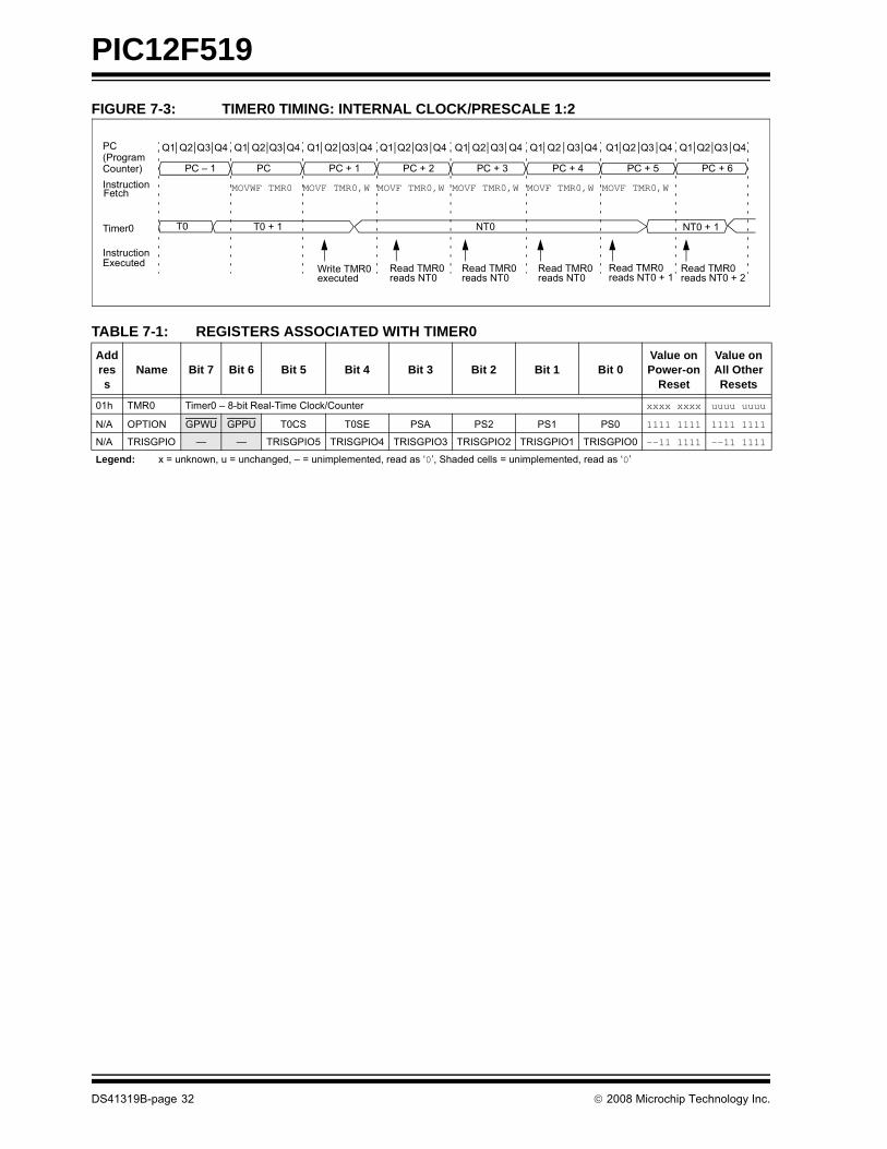
PIC12F519
FIGURE 7-3: TIMER0 TIMING: INTERNAL CLOCK/PRESCALE 1:2TABLE 7-1: REGISTERS ASSOCIATED WITH TIMER0Address
Name Bit 7 Bit 6 Bit 5 Bit 4 Bit 3 Bit 2 Bit 1 Bit 0Value onPower-on
Reset
Value onAll Other Resets
01h TMR0 Timer0 – 8-bit Real-Time Clock/Counter xxxx xxxx uuuu uuuu
N/A OPTION GPWU GPPU T0CS T0SE PSA PS2 PS1 PS0 1111 1111 1111 1111
N/A TRISGPIO — — TRISGPIO5 TRISGPIO4 TRISGPIO3 TRISGPIO2 TRISGPIO1 TRISGPIO0 --11 1111 --11 1111
Legend: x = unknown, u = unchanged, – = unimplemented, read as ‘0’, Shaded cells = unimplemented, read as ‘0’
PC – 1
Q1 Q2 Q3 Q4 Q1 Q2 Q3 Q4 Q1 Q2 Q3 Q4 Q1 Q2 Q3 Q4 Q1 Q2 Q3 Q4 Q1 Q2 Q3 Q4 Q1 Q2 Q3 Q4 Q1 Q2 Q3 Q4
InstructionFetch
Timer0
PC PC + 1 PC + 2 PC + 3 PC + 4 PC + 6
T0 T0 + 1 NT0 NT0 + 1
MOVWF TMR0 MOVF TMR0,W MOVF TMR0,W MOVF TMR0,W MOVF TMR0,W MOVF TMR0,W
Write TMR0executed
Read TMR0reads NT0
Read TMR0reads NT0
Read TMR0reads NT0
Read TMR0reads NT0 + 1
Read TMR0reads NT0 + 2
InstructionExecuted
PC + 5
PC(ProgramCounter)
DS41319B-page 32 © 2008 Microchip Technology Inc.
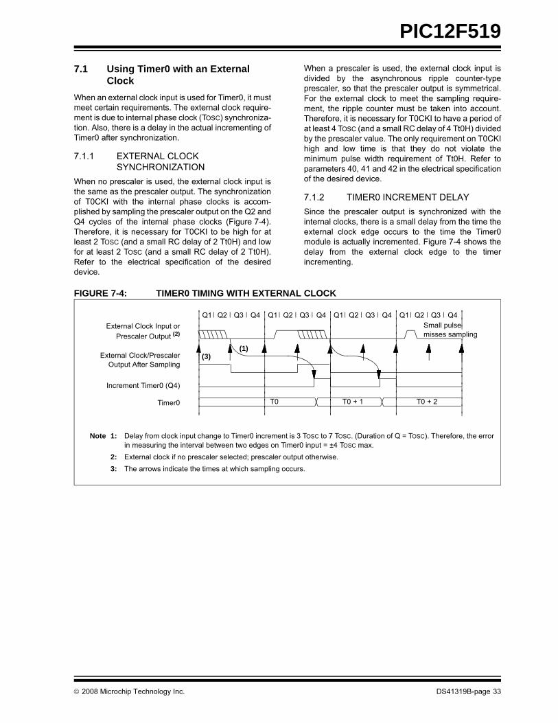
PIC12F519
7.1 Using Timer0 with an ExternalClockWhen an external clock input is used for Timer0, it mustmeet certain requirements. The external clock require-ment is due to internal phase clock (TOSC) synchroniza-tion. Also, there is a delay in the actual incrementing ofTimer0 after synchronization.
7.1.1 EXTERNAL CLOCK SYNCHRONIZATION
When no prescaler is used, the external clock input isthe same as the prescaler output. The synchronizationof T0CKI with the internal phase clocks is accom-plished by sampling the prescaler output on the Q2 andQ4 cycles of the internal phase clocks (Figure 7-4).Therefore, it is necessary for T0CKI to be high for atleast 2 TOSC (and a small RC delay of 2 Tt0H) and lowfor at least 2 TOSC (and a small RC delay of 2 Tt0H).Refer to the electrical specification of the desireddevice.
When a prescaler is used, the external clock input isdivided by the asynchronous ripple counter-typeprescaler, so that the prescaler output is symmetrical.For the external clock to meet the sampling require-ment, the ripple counter must be taken into account.Therefore, it is necessary for T0CKI to have a period ofat least 4 TOSC (and a small RC delay of 4 Tt0H) dividedby the prescaler value. The only requirement on T0CKIhigh and low time is that they do not violate theminimum pulse width requirement of Tt0H. Refer toparameters 40, 41 and 42 in the electrical specificationof the desired device.
7.1.2 TIMER0 INCREMENT DELAYSince the prescaler output is synchronized with theinternal clocks, there is a small delay from the time theexternal clock edge occurs to the time the Timer0module is actually incremented. Figure 7-4 shows thedelay from the external clock edge to the timerincrementing.
FIGURE 7-4: TIMER0 TIMING WITH EXTERNAL CLOCK
Increment Timer0 (Q4)
External Clock Input orQ1 Q2 Q3 Q4 Q1 Q2 Q3 Q4 Q1 Q2 Q3 Q4 Q1 Q2 Q3 Q4
Timer0 T0 T0 + 1 T0 + 2
Small pulse misses sampling
External Clock/PrescalerOutput After Sampling
(3)
Prescaler Output (2)
(1)
Note 1: Delay from clock input change to Timer0 increment is 3 TOSC to 7 TOSC. (Duration of Q = TOSC). Therefore, the errorin measuring the interval between two edges on Timer0 input = ±4 TOSC max.
2: External clock if no prescaler selected; prescaler output otherwise. 3: The arrows indicate the times at which sampling occurs.
© 2008 Microchip Technology Inc. DS41319B-page 33
PIC12F519
7.2 PrescalerAn 8-bit counter is available as a prescaler for theTimer0 module or as a postscaler for the WatchdogTimer (WDT), respectively (see Section 8.6 “Watch-dog Timer (WDT)”). For simplicity, this counter isbeing referred to as “prescaler” throughout this datasheet.The PSA and PS<2:0> bits (OPTION<3:0>) determineprescaler assignment and prescale ratio.
When assigned to the Timer0 module, all instructionswriting to the TMR0 register (e.g., CLRF TMR0,MOVWF TMR0, etc.) will clear the prescaler. Whenassigned to WDT, a CLRWDT instruction will clear theprescaler along with the WDT. The prescaler is neitherreadable nor writable. On a Reset, the prescaler con-tains all ‘0’s.
7.2.1 SWITCHING PRESCALER ASSIGNMENT
The prescaler assignment is fully under softwarecontrol (i.e., it can be changed “on-the-fly” during pro-gram execution). To avoid an unintended device Reset,the following instruction sequence (Example 7-1) mustbe executed when changing the prescaler assignmentfrom Timer0 to the WDT.
EXAMPLE 7-1: CHANGING PRESCALER (TIMER0 → WDT)
To change the prescaler from the WDT to the Timer0module, use the sequence shown in Example 7-2. Thissequence must be used even if the WDT is disabled. ACLRWDT instruction should be executed beforeswitching the prescaler.
EXAMPLE 7-2: CHANGING PRESCALER (WDT → TIMER0)
Note: The prescaler may be used by either theTimer0 module or the WDT, but not both.Thus, a prescaler assignment for theTimer0 module means that there is noprescaler for the WDT and vice versa.
CLRWDT ;Clear WDTCLRF TMR0 ;Clear TMR0 and Prescaler MOVLW b‘00xx1111’OPTION
CLRWDT ;PS<2:0> are 000 or 001MOVLW b‘00xx1xxx’ ;Set Postscaler toOPTION ;desired WDT rate
CLRWDT ;Clear WDT and ;prescaler
MOVLW b‘xxxx0xxx’ ;Select TMR0, new ;prescale value and;clock source
OPTION
DS41319B-page 34 © 2008 Microchip Technology Inc.
PIC12F519
FIGURE 7-5: BLOCK DIAGRAM OF THE TIMER0/ WDT PRESCALER(1)T0CKI
T0SE
pin
TCY (= FOSC/4)
Sync2
CyclesTMR0 Reg
8-bit Prescaler
8-to-1 MUX
M
MUX
WatchdogTimer
PSA
0 1
0
1
WDTTime-Out
PS<2:0>
8
PSAWDT Enable bit
0
1
0
1
Data Bus
8
PSAT0CS
MUX M
UX
UX
Note 1: T0CS, T0SE, PSA, PS<2:0> are bits in the OPTION register.
© 2008 Microchip Technology Inc. DS41319B-page 35

PIC12F519
NOTES:DS41319B-page 36 © 2008 Microchip Technology Inc.
PIC12F519
8.0 SPECIAL FEATURES OF THE CPU
What sets a microcontroller apart from other processorsare special circuits that deal with the needs of real-timeapplications. The PIC12F519 microcontroller has a hostof such features intended to maximize system reliability,minimize cost through elimination of externalcomponents, provide power-saving operating modesand offer code protection. These features are:
• Oscillator Selection• Reset:
- Power-on Reset (POR)- Device Reset Timer (DRT)- Wake-up from Sleep on Pin Change
• Watchdog Timer (WDT)• Sleep• Code Protection• ID Locations• In-Circuit Serial Programming™
The PIC12F519 device has a Watchdog Timer, whichcan be shut off only through Configuration bit WDTE. Itruns off of its own RC oscillator for added reliability. Ifusing XT or LP selectable oscillator options, there isalways an 18 ms (nominal) delay provided by theDevice Reset Timer (DRT), intended to keep the chip inReset until the crystal oscillator is stable. If using INTRCor EXTRC, the DRT provides a 1 ms (nominal) delay.
The Sleep mode is designed to offer a very low-currentPower-Down mode. The user can wake-up from Sleepthrough a change-on-input-pins or through a WatchdogTimer time-out. Several oscillator options are also madeavailable to allow the part to fit the application, includingan internal 4 MHz or 8 MHz oscillator. The EXTRCoscillator option saves system cost while the LP crystaloption saves power. A set of Configuration bits are usedto select various options.
8.1 Configuration BitsThe PIC12F519 Configuration Words consist of 12 bits.Configuration bits can be programmed to select variousdevice configurations. Two bits are for the selection ofthe oscillator type; one bit is the Watchdog Timer enablebit, one bit is the MCLR enable bit and one bit is for codeprotection (Register 8-1).
© 2008 Microchip Technology Inc. DS41319B-page 37
PIC12F519
REGISTER 8-1: CONFIG: CONFIGURATION WORD REGISTER(1)— CPDF IOSCFS MCLRE CP WDTE FOSC1 FOSC0bit 7 bit 0
bit 7 Unimplemented: Read as ‘1’bit 6 CPDF: Code Protection bit - Flash Data Memory
1 = Code protection off0 = Code protection on
bit 5 IOSCFS: Internal Oscillator Frequency Select bit1 = 8 MHz INTOSC frequency0 = 4 MHz INTOSC frequency
bit 4 MCLRE: Master Clear Enable bit1 = GP3/MCLR pin functions as MCLR0 = GP3/MCLR pin functions as GP3, MCLR internally tied to VDD
bit 3 CP: Code Protection bit - User Program Memory1 = Code protection off0 = Code protection on
bit 2 WDTE: Watchdog Timer Enable bit 1 = WDT enabled0 = WDT disabled
bit 1-0 FOSC<1:0>: Oscillator Selection bits00 = LP oscillator with 18 ms DRT(2)
01 = XT oscillator with 18 ms DRT(2)
10 = INTOSC with 1 ms DRT(2)
11 = EXTRC with 1 ms DRT(2)
Note 1: Refer to the “PIC12F519 Memory Programming Specification”, DS41316 to determine how toprogram/erase the Configuration Word.
2: DRT length (18 ms or 1 ms) is a function of clock mode selection. It is the responsibility of the applicationdesigner to ensure the use of either 18 ms (nominal) DRT or the 1 ms (nominal) DRT will result inacceptable operation. Refer to Figure 11-1 and Table 11-2 for VDD rise time and stability requirements forthis mode of operation.
DS41319B-page 38 © 2008 Microchip Technology Inc.
PIC12F519
8.2 Oscillator Configurations8.2.1 OSCILLATOR TYPESThe PIC12F519 device can be operated in up to fourdifferent oscillator modes. The user can program usingthe Configuration bits (FOSC<1:0>), to select one ofthese modes:
• LP: Low-Power Crystal• XT: Crystal/Resonator• INTRC: Internal 4 MHz or 8 MHz Oscillator• EXTRC: External Resistor/Capacitor
8.2.2 CRYSTAL OSCILLATOR/CERAMIC RESONATORS
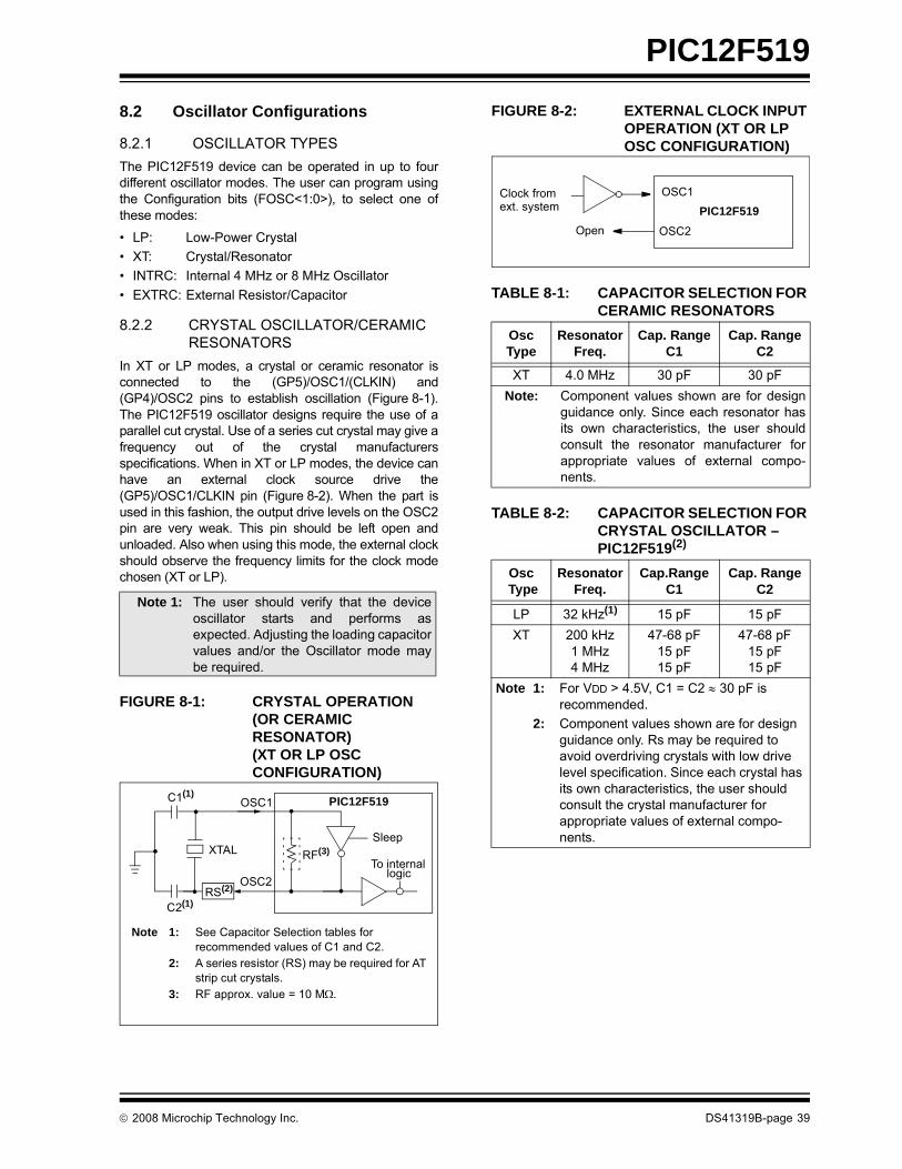
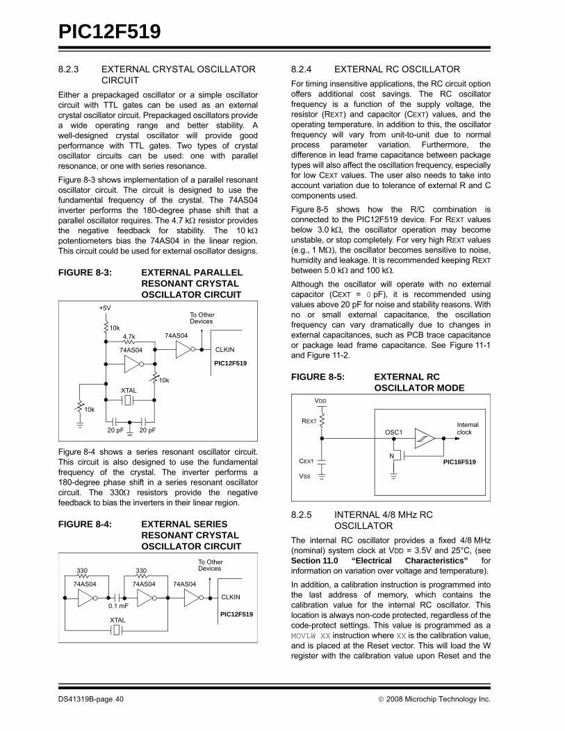
In XT or LP modes, a crystal or ceramic resonator isconnected to the (GP5)/OSC1/(CLKIN) and(GP4)/OSC2 pins to establish oscillation (Figure 8-1).The PIC12F519 oscillator designs require the use of aparallel cut crystal. Use of a series cut crystal may give afrequency out of the crystal manufacturersspecifications. When in XT or LP modes, the device canhave an external clock source drive the(GP5)/OSC1/CLKIN pin (Figure 8-2). When the part isused in this fashion, the output drive levels on the OSC2pin are very weak. This pin should be left open andunloaded. Also when using this mode, the external clockshould observe the frequency limits for the clock modechosen (XT or LP).
FIGURE 8-1: CRYSTAL OPERATION (OR CERAMIC RESONATOR) (XT OR LP OSC CONFIGURATION)
FIGURE 8-2: EXTERNAL CLOCK INPUT OPERATION (XT OR LP OSC CONFIGURATION)
TABLE 8-1: CAPACITOR SELECTION FOR CERAMIC RESONATORS
TABLE 8-2: CAPACITOR SELECTION FOR CRYSTAL OSCILLATOR – PIC12F519(2)
Note 1: The user should verify that the deviceoscillator starts and performs asexpected. Adjusting the loading capacitorvalues and/or the Oscillator mode maybe required.
Note 1: See Capacitor Selection tables for recommended values of C1 and C2.
2: A series resistor (RS) may be required for AT strip cut crystals.
3: RF approx. value = 10 MΩ.
C1(1)
C2(1)
XTAL
OSC2
OSC1
RF(3)Sleep
To internallogic
RS(2)
PIC12F519
OscType
Resonator Freq.
Cap. RangeC1
Cap. RangeC2
XT 4.0 MHz 30 pF 30 pFNote: Component values shown are for design
guidance only. Since each resonator hasits own characteristics, the user shouldconsult the resonator manufacturer forappropriate values of external compo-nents.
Osc Type
Resonator Freq.
Cap.RangeC1
Cap. RangeC2
LP 32 kHz(1) 15 pF 15 pFXT 200 kHz
1 MHz4 MHz
47-68 pF15 pF15 pF
47-68 pF15 pF15 pF
Note 1: For VDD > 4.5V, C1 = C2 ≈ 30 pF is recommended.
2: Component values shown are for design guidance only. Rs may be required to avoid overdriving crystals with low drive level specification. Since each crystal has its own characteristics, the user should consult the crystal manufacturer for appropriate values of external compo-nents.
Clock fromext. system
OSC1
OSC2OpenPIC12F519
© 2008 Microchip Technology Inc. DS41319B-page 39
PIC12F519
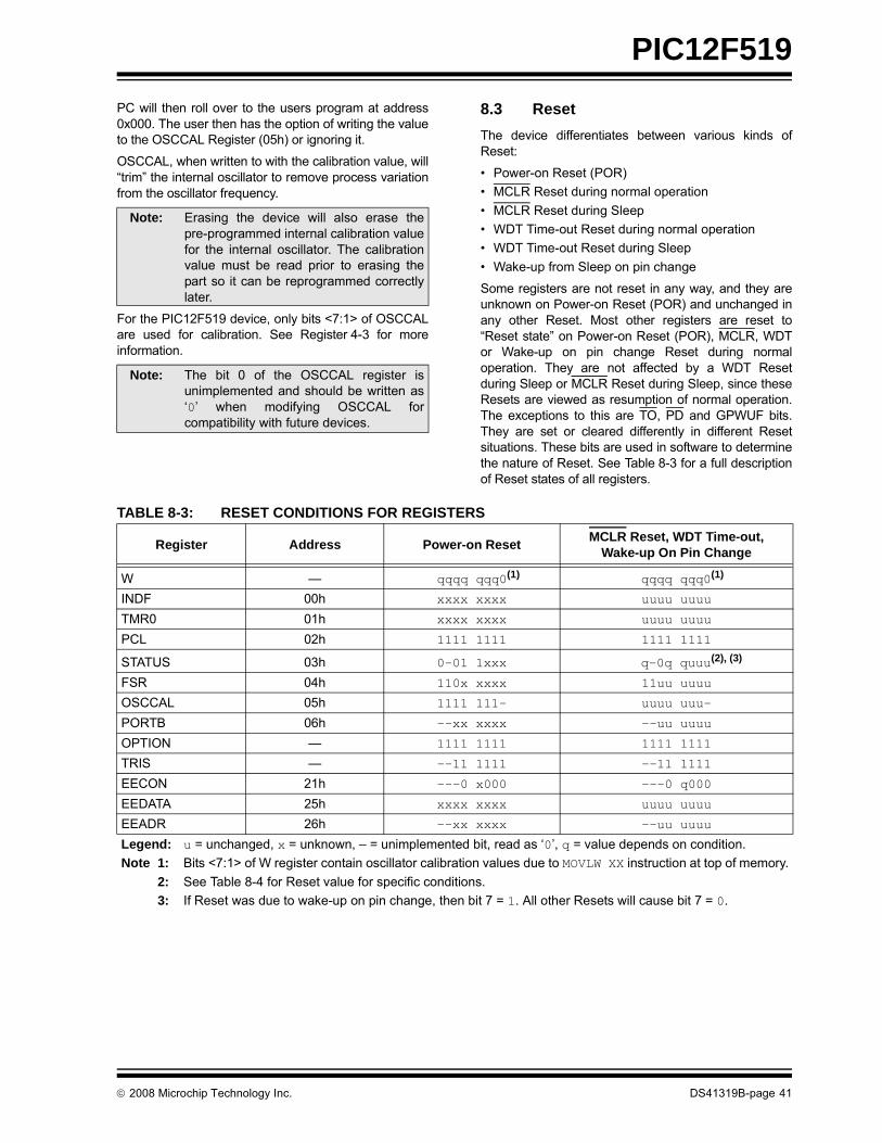
8.2.3 EXTERNAL CRYSTAL OSCILLATORCIRCUITEither a prepackaged oscillator or a simple oscillatorcircuit with TTL gates can be used as an externalcrystal oscillator circuit. Prepackaged oscillators providea wide operating range and better stability. Awell-designed crystal oscillator will provide goodperformance with TTL gates. Two types of crystaloscillator circuits can be used: one with parallelresonance, or one with series resonance.
Figure 8-3 shows implementation of a parallel resonantoscillator circuit. The circuit is designed to use thefundamental frequency of the crystal. The 74AS04inverter performs the 180-degree phase shift that aparallel oscillator requires. The 4.7 kΩ resistor providesthe negative feedback for stability. The 10 kΩpotentiometers bias the 74AS04 in the linear region.This circuit could be used for external oscillator designs.
FIGURE 8-3: EXTERNAL PARALLEL RESONANT CRYSTAL OSCILLATOR CIRCUIT
Figure 8-4 shows a series resonant oscillator circuit.This circuit is also designed to use the fundamentalfrequency of the crystal. The inverter performs a180-degree phase shift in a series resonant oscillatorcircuit. The 330Ω resistors provide the negativefeedback to bias the inverters in their linear region.
FIGURE 8-4: EXTERNAL SERIES RESONANT CRYSTAL OSCILLATOR CIRCUIT
8.2.4 EXTERNAL RC OSCILLATORFor timing insensitive applications, the RC circuit optionoffers additional cost savings. The RC oscillatorfrequency is a function of the supply voltage, theresistor (REXT) and capacitor (CEXT) values, and theoperating temperature. In addition to this, the oscillatorfrequency will vary from unit-to-unit due to normalprocess parameter variation. Furthermore, thedifference in lead frame capacitance between packagetypes will also affect the oscillation frequency, especiallyfor low CEXT values. The user also needs to take intoaccount variation due to tolerance of external R and Ccomponents used.
Figure 8-5 shows how the R/C combination isconnected to the PIC12F519 device. For REXT valuesbelow 3.0 kΩ, the oscillator operation may becomeunstable, or stop completely. For very high REXT values(e.g., 1 MΩ), the oscillator becomes sensitive to noise,humidity and leakage. It is recommended keeping REXTbetween 5.0 kΩ and 100 kΩ.
Although the oscillator will operate with no externalcapacitor (CEXT = 0 pF), it is recommended usingvalues above 20 pF for noise and stability reasons. Withno or small external capacitance, the oscillationfrequency can vary dramatically due to changes inexternal capacitances, such as PCB trace capacitanceor package lead frame capacitance. See Figure 11-1and Figure 11-2.
FIGURE 8-5: EXTERNAL RC OSCILLATOR MODE
8.2.5 INTERNAL 4/8 MHz RC OSCILLATOR
The internal RC oscillator provides a fixed 4/8 MHz(nominal) system clock at VDD = 3.5V and 25°C, (seeSection 11.0 “Electrical Characteristics” forinformation on variation over voltage and temperature).
In addition, a calibration instruction is programmed intothe last address of memory, which contains thecalibration value for the internal RC oscillator. Thislocation is always non-code protected, regardless of thecode-protect settings. This value is programmed as aMOVLW XX instruction where XX is the calibration value,and is placed at the Reset vector. This will load the Wregister with the calibration value upon Reset and the
20 pF
+5V
20 pF
10k4.7k
10k
74AS04
XTAL
10k
74AS04
PIC12F519
CLKIN
To OtherDevices
330
74AS04 74AS04
CLKIN
To OtherDevices
XTAL
330
74AS04
0.1 mFPIC12F519
VDD
REXT
CEXT
VSS
OSC1Internalclock
PIC16F519N
DS41319B-page 40 © 2008 Microchip Technology Inc.
PIC12F519
PC will then roll over to the users program at address0x000. The user then has the option of writing the valueto the OSCCAL Register (05h) or ignoring it.OSCCAL, when written to with the calibration value, will“trim” the internal oscillator to remove process variationfrom the oscillator frequency.
For the PIC12F519 device, only bits <7:1> of OSCCALare used for calibration. See Register 4-3 for moreinformation.
8.3 ResetThe device differentiates between various kinds ofReset:
• Power-on Reset (POR) • MCLR Reset during normal operation• MCLR Reset during Sleep • WDT Time-out Reset during normal operation• WDT Time-out Reset during Sleep• Wake-up from Sleep on pin change
Some registers are not reset in any way, and they areunknown on Power-on Reset (POR) and unchanged inany other Reset. Most other registers are reset to“Reset state” on Power-on Reset (POR), MCLR, WDTor Wake-up on pin change Reset during normaloperation. They are not affected by a WDT Resetduring Sleep or MCLR Reset during Sleep, since theseResets are viewed as resumption of normal operation.The exceptions to this are TO, PD and GPWUF bits.They are set or cleared differently in different Resetsituations. These bits are used in software to determinethe nature of Reset. See Table 8-3 for a full descriptionof Reset states of all registers.
TABLE 8-3: RESET CONDITIONS FOR REGISTERS
Note: Erasing the device will also erase thepre-programmed internal calibration valuefor the internal oscillator. The calibrationvalue must be read prior to erasing thepart so it can be reprogrammed correctlylater.
Note: The bit 0 of the OSCCAL register isunimplemented and should be written as‘0’ when modifying OSCCAL forcompatibility with future devices.
Register Address Power-on Reset MCLR Reset, WDT Time-out, Wake-up On Pin Change
W — qqqq qqq0(1) qqqq qqq0(1)
INDF 00h xxxx xxxx uuuu uuuu
TMR0 01h xxxx xxxx uuuu uuuu
PCL 02h 1111 1111 1111 1111
STATUS 03h 0-01 1xxx q-0q quuu(2), (3)
FSR 04h 110x xxxx 11uu uuuu
OSCCAL 05h 1111 111- uuuu uuu-
PORTB 06h --xx xxxx --uu uuuu
OPTION — 1111 1111 1111 1111
TRIS — --11 1111 --11 1111
EECON 21h ---0 x000 ---0 q000
EEDATA 25h xxxx xxxx uuuu uuuu
EEADR 26h --xx xxxx --uu uuuu
Legend: u = unchanged, x = unknown, – = unimplemented bit, read as ‘0’, q = value depends on condition.Note 1: Bits <7:1> of W register contain oscillator calibration values due to MOVLW XX instruction at top of memory.
2: See Table 8-4 for Reset value for specific conditions.3: If Reset was due to wake-up on pin change, then bit 7 = 1. All other Resets will cause bit 7 = 0.
© 2008 Microchip Technology Inc. DS41319B-page 41
PIC12F519
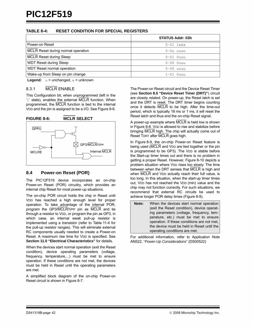
TABLE 8-4: RESET CONDITION FOR SPECIAL REGISTERS8.3.1 MCLR ENABLEThis Configuration bit, when unprogrammed (left in the‘1’ state), enables the external MCLR function. Whenprogrammed, the MCLR function is tied to the internalVDD and the pin is assigned to be a I/O. See Figure 8-6.
FIGURE 8-6: MCLR SELECT
8.4 Power-on Reset (POR)The PIC12F519 device incorporates an on-chipPower-on Reset (POR) circuitry, which provides aninternal chip Reset for most power-up situations.
The on-chip POR circuit holds the chip in Reset untilVDD has reached a high enough level for properoperation. To take advantage of the internal POR,program the GP3/MCLR/VPP pin as MCLR and tiethrough a resistor to VDD, or program the pin as GP3, inwhich case, an internal weak pull-up resistor isimplemented using a transistor (refer to Table 11-4 forthe pull-up resistor ranges). This will eliminate externalRC components usually needed to create a Power-onReset. A maximum rise time for VDD is specified. SeeSection 11.0 “Electrical Characteristics” for details.
When the devices start normal operation (exit the Resetcondition), device operating parameters (voltage,frequency, temperature,...) must be met to ensureoperation. If these conditions are not met, the devicesmust be held in Reset until the operating parametersare met.
A simplified block diagram of the on-chip Power-onReset circuit is shown in Figure 8-7.
The Power-on Reset circuit and the Device Reset Timer(see Section 8.5 “Device Reset Timer (DRT)”) circuitare closely related. On power-up, the Reset latch is setand the DRT is reset. The DRT timer begins countingonce it detects MCLR to be high. After the time-outperiod, which is typically 18 ms or 1 ms, it will reset theReset latch and thus end the on-chip Reset signal.
A power-up example where MCLR is held low is shownin Figure 8-8. VDD is allowed to rise and stabilize beforebringing MCLR high. The chip will actually come out ofReset TDRT after MCLR goes high.
In Figure 8-9, the on-chip Power-on Reset feature isbeing used (MCLR and VDD are tied together or the pinis programmed to be GP3). The VDD is stable beforethe Start-up timer times out and there is no problem ingetting a proper Reset. However, Figure 8-10 depicts aproblem situation where VDD rises too slowly. The timebetween when the DRT senses that MCLR is high andwhen MCLR and VDD actually reach their full value, istoo long. In this situation, when the start-up timer timesout, VDD has not reached the VDD (min) value and thechip may not function correctly. For such situations, werecommend that external RC circuits be used toachieve longer POR delay times (Figure 8-9).
For additional information, refer to Application NoteAN522, “Power-Up Considerations” (DS00522)
STATUS Addr: 03h
Power-on Reset 0-01 1xxx
MCLR Reset during normal operation 0-0u uuuu
MCLR Reset during Sleep 0-01 0uuu
WDT Reset during Sleep 0-00 0uuu
WDT Reset normal operation 0-00 uuuu
Wake-up from Sleep on pin change 1-01 0uuu
Legend: u = unchanged, x = unknown
GP3/MCLR/VPP
MCLRE Internal MCLR
GPPU
Note: When the devices start normal operation(exit the Reset condition), device operat-ing parameters (voltage, frequency, tem-perature, etc.) must be met to ensureoperation. If these conditions are not met,the device must be held in Reset until theoperating conditions are met.
DS41319B-page 42 © 2008 Microchip Technology Inc.
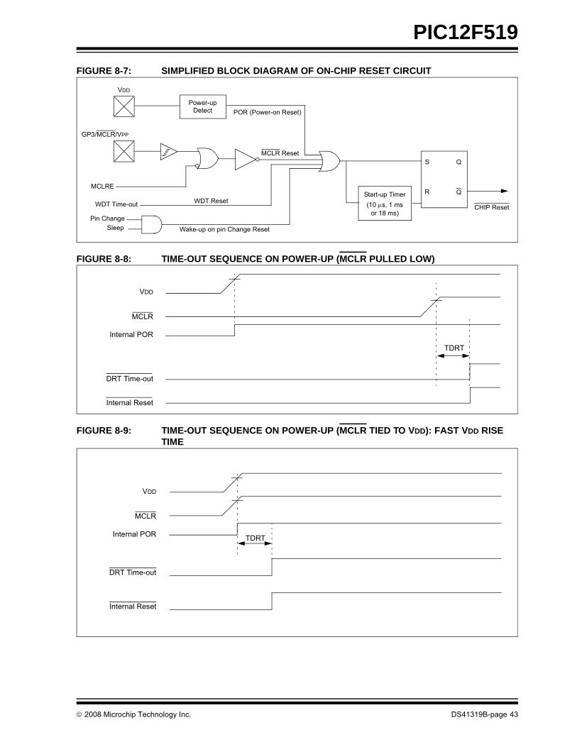
PIC12F519
FIGURE 8-7: SIMPLIFIED BLOCK DIAGRAM OF ON-CHIP RESET CIRCUITFIGURE 8-8: TIME-OUT SEQUENCE ON POWER-UP (MCLR PULLED LOW)
FIGURE 8-9: TIME-OUT SEQUENCE ON POWER-UP (MCLR TIED TO VDD): FAST VDD RISE TIME
S Q
R Q
VDD
GP3/MCLR/VPP
Power-upDetect POR (Power-on Reset)
WDT ResetCHIP Reset
MCLRE
Wake-up on pin Change Reset
Start-up Timer(10 μs, 1 msWDT Time-out
Pin ChangeSleep
MCLR Reset
or 18 ms)
VDD
MCLR
Internal POR
DRT Time-out
Internal Reset
TDRT
VDD
MCLR
Internal POR
DRT Time-out
Internal Reset
TDRT
© 2008 Microchip Technology Inc. DS41319B-page 43
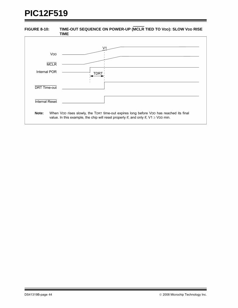
PIC12F519
FIGURE 8-10: TIME-OUT SEQUENCE ON POWER-UP (MCLR TIED TO VDD): SLOW VDD RISETIME
VDD
MCLR
Internal POR
DRT Time-out
Internal Reset
TDRT
V1
Note: When VDD rises slowly, the TDRT time-out expires long before VDD has reached its finalvalue. In this example, the chip will reset properly if, and only if, V1 ≥ VDD min.
DS41319B-page 44 © 2008 Microchip Technology Inc.
PIC12F519
8.5 Device Reset Timer (DRT)On the PIC12F519 device, the DRT runs any time thedevice is powered up. DRT runs from Reset and variesbased on oscillator selection and Reset type (seeTable 8-5).The DRT operates on an internal RC oscillator. Theprocessor is kept in Reset as long as the DRT is active.The DRT delay allows VDD to rise above VDD min. andfor the oscillator to stabilize.
Oscillator circuits based on crystals or ceramicresonators require a certain time after power-up toestablish a stable oscillation. The on-chip DRT keepsthe devices in a Reset condition after MCLR hasreached a logic high (VIH MCLR) level. ProgrammingGP3/MCLR/VPP as MCLR and using an external RCnetwork connected to the MCLR input is not required inmost cases. This allows savings in cost-sensitive and/orspace restricted applications, as well as allowing theuse of the GP3/MCLR/VPP pin as a general purposeinput.
The Device Reset Time delays will vary fromchip-to-chip due to VDD, temperature and processvariation. See AC parameters for details.
The DRT will also be triggered upon a Watchdog Timertime-out from Sleep. This is particularly important forapplications using the WDT to wake from Sleep modeautomatically.
Reset sources are POR, MCLR, WDT time-out andwake-up on pin change. See Section 8.8.2 “Wake-upfrom Sleep”, Notes 1, 2 and 3.
TABLE 8-5: DRT (DEVICE RESET TIMER PERIOD)
8.6 Watchdog Timer (WDT)The Watchdog Timer (WDT) is a free running on-chipRC oscillator, which does not require any externalcomponents. This RC oscillator is separate from theexternal RC oscillator of the (GP5)/OSC1/CLKIN pinand the internal 4 or 8 MHz oscillator. This means thatthe WDT will run even if the main processor clock hasbeen stopped, for example, by execution of a SLEEPinstruction. During normal operation or Sleep, a WDTReset or wake-up Reset, generates a device Reset.
The TO bit (STATUS<4>) will be cleared upon aWatchdog Timer Reset.
The WDT can be permanently disabled byprogramming the configuration WDTE as a ‘0’ (seeSection 8.1 “Configuration Bits”). Refer to thePIC12F519 Programming Specification (DS41316) todetermine how to access the Configuration Word.
8.6.1 WDT PERIODThe WDT has a nominal time-out period of 18 ms, (withno prescaler). If a longer time-out period is desired, aprescaler with a division ratio of up to 1:128 can beassigned to the WDT (under software control) by writingto the OPTION register. Thus, a time-out period of anominal 2.3 seconds can be realized. These periodsvary with temperature, VDD and part-to-part processvariations (see DC specs).
Under worst-case conditions (VDD = Min., Temperature= Max., max. WDT prescaler), it may take severalseconds before a WDT time-out occurs.
8.6.2 WDT PROGRAMMING CONSIDERATIONS
The CLRWDT instruction clears the WDT and thepostscaler, if assigned to the WDT, and prevents it fromtiming out and generating a device Reset.
The SLEEP instruction resets the WDT and thepostscaler, if assigned to the WDT. This gives themaximum Sleep time before a WDT wake-up Reset.
Oscillator Configuration POR Reset Subsequent
Resets
INTOSC, EXTRC 1 ms (typical) 10 μs (typical)
LP, XT 18 ms (typical) 18 ms (typical)
© 2008 Microchip Technology Inc. DS41319B-page 45
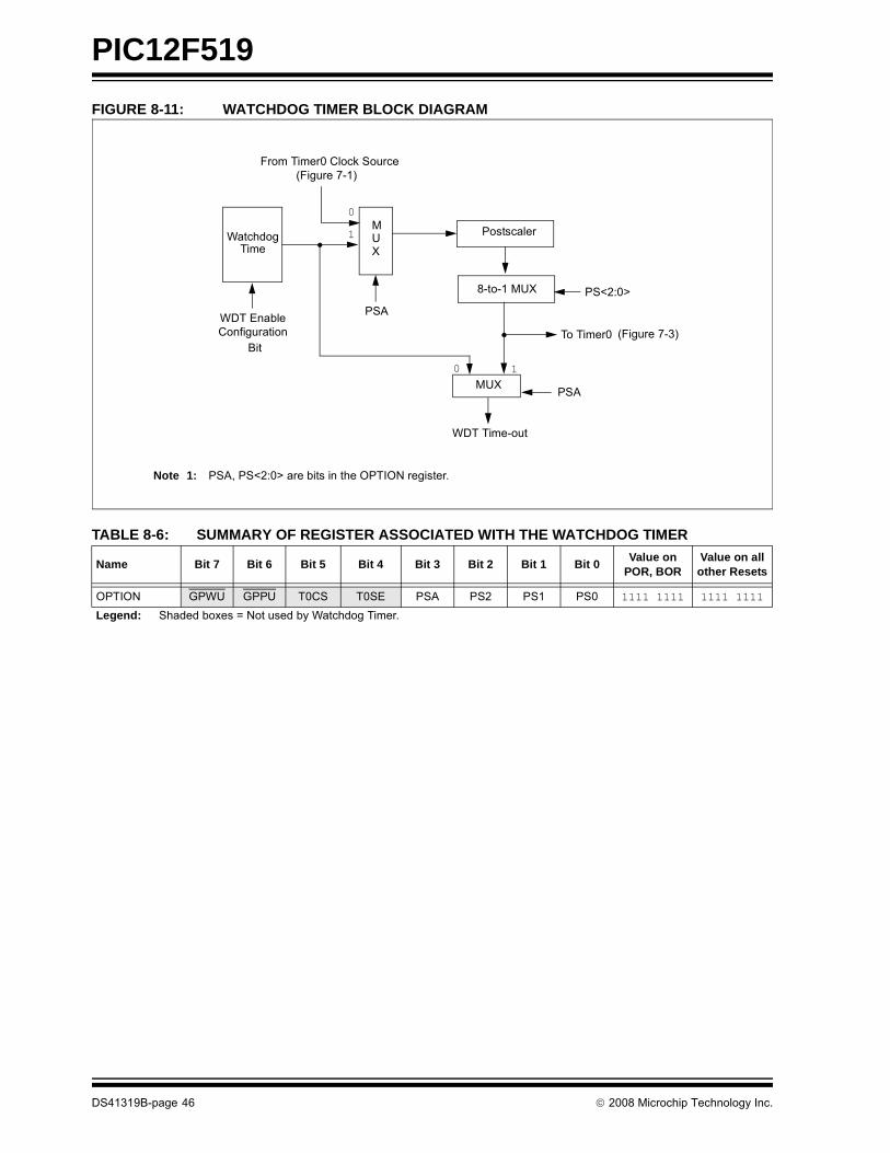
PIC12F519
FIGURE 8-11: WATCHDOG TIMER BLOCK DIAGRAMTABLE 8-6: SUMMARY OF REGISTER ASSOCIATED WITH THE WATCHDOG TIMER
Name Bit 7 Bit 6 Bit 5 Bit 4 Bit 3 Bit 2 Bit 1 Bit 0 Value on POR, BOR
Value on all other Resets
OPTION GPWU GPPU T0CS T0SE PSA PS2 PS1 PS0 1111 1111 1111 1111
Legend: Shaded boxes = Not used by Watchdog Timer.
(Figure 7-1)
Postscaler
Note 1: PSA, PS<2:0> are bits in the OPTION register.
WDT Time-out
WatchdogTime
From Timer0 Clock Source
WDT EnableConfiguration
Bit
PSA
Postscaler
8-to-1 MUX PS<2:0>
(Figure 7-3)To Timer0
0
1MUX
10
PSAMUX
DS41319B-page 46 © 2008 Microchip Technology Inc.
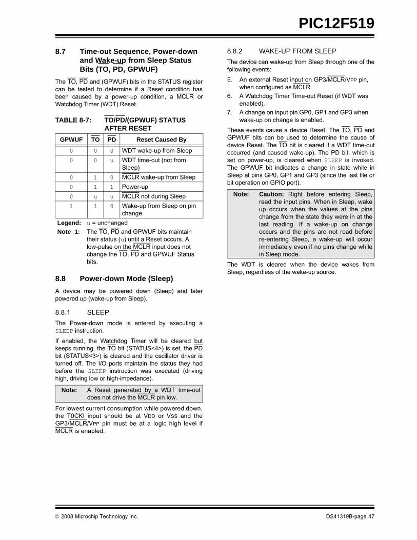
PIC12F519
8.7 Time-out Sequence, Power-downand Wake-up from Sleep Status Bits (TO, PD, GPWUF)
The TO, PD and (GPWUF) bits in the STATUS registercan be tested to determine if a Reset condition hasbeen caused by a power-up condition, a MCLR orWatchdog Timer (WDT) Reset.
TABLE 8-7: TO/PD/(GPWUF) STATUS AFTER RESET
8.8 Power-down Mode (Sleep) A device may be powered down (Sleep) and laterpowered up (wake-up from Sleep).
8.8.1 SLEEPThe Power-down mode is entered by executing aSLEEP instruction.
If enabled, the Watchdog Timer will be cleared butkeeps running, the TO bit (STATUS<4>) is set, the PDbit (STATUS<3>) is cleared and the oscillator driver isturned off. The I/O ports maintain the status they hadbefore the SLEEP instruction was executed (drivinghigh, driving low or high-impedance).
For lowest current consumption while powered down,the T0CKI input should be at VDD or VSS and theGP3/MCLR/VPP pin must be at a logic high level ifMCLR is enabled.
8.8.2 WAKE-UP FROM SLEEPThe device can wake-up from Sleep through one of thefollowing events:
5. An external Reset input on GP3/MCLR/VPP pin,when configured as MCLR.
6. A Watchdog Timer Time-out Reset (if WDT wasenabled).
7. A change on input pin GP0, GP1 and GP3 whenwake-up on change is enabled.
These events cause a device Reset. The TO, PD andGPWUF bits can be used to determine the cause ofdevice Reset. The TO bit is cleared if a WDT time-outoccurred (and caused wake-up). The PD bit, which isset on power-up, is cleared when SLEEP is invoked.The GPWUF bit indicates a change in state while inSleep at pins GP0, GP1 and GP3 (since the last file orbit operation on GPIO port).
The WDT is cleared when the device wakes fromSleep, regardless of the wake-up source.
GPWUF TO PD Reset Caused By
0 0 0 WDT wake-up from Sleep0 0 u WDT time-out (not from
Sleep)0 1 0 MCLR wake-up from Sleep0 1 1 Power-up0 u u MCLR not during Sleep1 1 0 Wake-up from Sleep on pin
changeLegend: u = unchangedNote 1: The TO, PD and GPWUF bits maintain
their status (u) until a Reset occurs. A low-pulse on the MCLR input does not change the TO, PD and GPWUF Status bits.
Note: A Reset generated by a WDT time-outdoes not drive the MCLR pin low.
Note: Caution: Right before entering Sleep,read the input pins. When in Sleep, wakeup occurs when the values at the pinschange from the state they were in at thelast reading. If a wake-up on changeoccurs and the pins are not read beforere-entering Sleep, a wake-up will occurimmediately even if no pins change whilein Sleep mode.
© 2008 Microchip Technology Inc. DS41319B-page 47
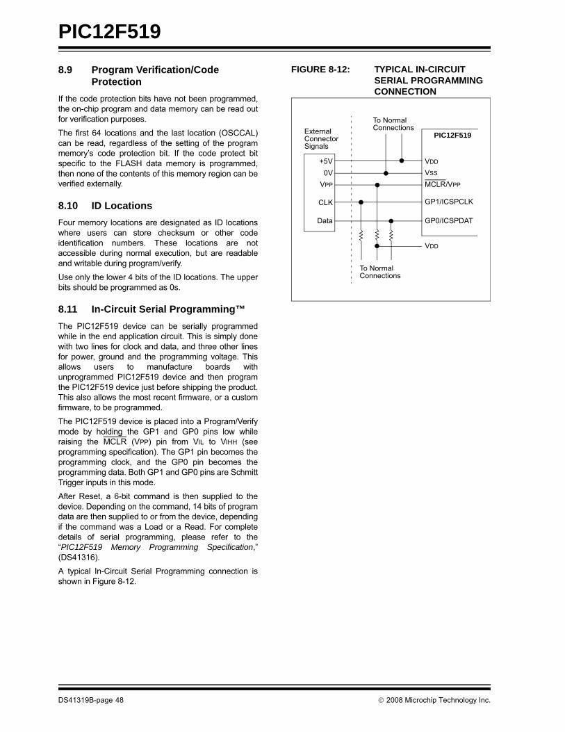
PIC12F519
8.9 Program Verification/CodeProtectionIf the code protection bits have not been programmed,the on-chip program and data memory can be read outfor verification purposes.
The first 64 locations and the last location (OSCCAL)can be read, regardless of the setting of the programmemory’s code protection bit. If the code protect bitspecific to the FLASH data memory is programmed,then none of the contents of this memory region can beverified externally.
8.10 ID LocationsFour memory locations are designated as ID locationswhere users can store checksum or other codeidentification numbers. These locations are notaccessible during normal execution, but are readableand writable during program/verify.
Use only the lower 4 bits of the ID locations. The upperbits should be programmed as 0s.
8.11 In-Circuit Serial Programming™The PIC12F519 device can be serially programmedwhile in the end application circuit. This is simply donewith two lines for clock and data, and three other linesfor power, ground and the programming voltage. Thisallows users to manufacture boards withunprogrammed PIC12F519 device and then programthe PIC12F519 device just before shipping the product.This also allows the most recent firmware, or a customfirmware, to be programmed.
The PIC12F519 device is placed into a Program/Verifymode by holding the GP1 and GP0 pins low whileraising the MCLR (VPP) pin from VIL to VIHH (seeprogramming specification). The GP1 pin becomes theprogramming clock, and the GP0 pin becomes theprogramming data. Both GP1 and GP0 pins are SchmittTrigger inputs in this mode.
After Reset, a 6-bit command is then supplied to thedevice. Depending on the command, 14 bits of programdata are then supplied to or from the device, dependingif the command was a Load or a Read. For completedetails of serial programming, please refer to the“PIC12F519 Memory Programming Specification,”(DS41316).
A typical In-Circuit Serial Programming connection isshown in Figure 8-12.
FIGURE 8-12: TYPICAL IN-CIRCUIT SERIAL PROGRAMMING CONNECTION
ExternalConnectorSignals
To NormalConnections
To NormalConnections
PIC12F519
VDD
VSS
MCLR/VPP
GP1/ICSPCLK
GP0/ICSPDAT
+5V0V
VPP
CLK
Data
VDD
DS41319B-page 48 © 2008 Microchip Technology Inc.
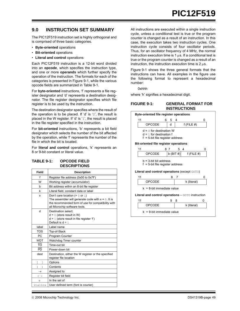
PIC12F519
9.0 INSTRUCTION SET SUMMARYThe PIC12F519 instruction set is highly orthogonal andis comprised of three basic categories.
• Byte-oriented operations• Bit-oriented operations• Literal and control operations
Each PIC12F519 instruction is a 12-bit word dividedinto an opcode, which specifies the instruction type,and one or more operands which further specify theoperation of the instruction. The formats for each of thecategories is presented in Figure 9-1, while the variousopcode fields are summarized in Table 9-1.
For byte-oriented instructions, ‘f’ represents a file reg-ister designator and ‘d’ represents a destination desig-nator. The file register designator specifies which fileregister is to be used by the instruction.
The destination designator specifies where the result ofthe operation is to be placed. If ‘d’ is ‘0’, the result isplaced in the W register. If ‘d’ is ‘1’, the result is placedin the file register specified in the instruction.
For bit-oriented instructions, ‘b’ represents a bit fielddesignator which selects the number of the bit affectedby the operation, while ‘f’ represents the number of thefile in which the bit is located.
For literal and control operations, ‘k’ represents an8 or 9-bit constant or literal value.
TABLE 9-1: OPCODE FIELD DESCRIPTIONS
All instructions are executed within a single instructioncycle, unless a conditional test is true or the programcounter is changed as a result of an instruction. In thiscase, the execution takes two instruction cycles. Oneinstruction cycle consists of four oscillator periods.Thus, for an oscillator frequency of 4 MHz, the normalinstruction execution time is 1 μs. If a conditional test istrue or the program counter is changed as a result of aninstruction, the instruction execution time is 2 μs.
Figure 9-1 shows the three general formats that theinstructions can have. All examples in the figure usethe following format to represent a hexadecimalnumber:
0xhhh
where ‘h’ signifies a hexadecimal digit.
FIGURE 9-1: GENERAL FORMAT FOR INSTRUCTIONS
Field Description
f Register file address (0x00 to 0x7F)W Working register (accumulator)b Bit address within an 8-bit file registerk Literal field, constant data or labelx Don’t care location (= 0 or 1)
The assembler will generate code with x = 0. It is the recommended form of use for compatibility with all Microchip software tools.
d Destination select; d = 0 (store result in W)d = 1 (store result in file register ‘f’)Default is d = 1
label Label nameTOS Top-of-StackPC Program Counter
WDT Watchdog Timer counterTO Time-out bitPD Power-down bitdest Destination, either the W register or the specified
register file location[ ] Options( ) Contents
→ Assigned to< > Register bit field
∈ In the set ofitalics User defined term (font is courier)
Byte-oriented file register operations
11 6 5 4 0
d = 0 for destination W
OPCODE d f (FILE #)
d = 1 for destination ff = 5-bit file register address
Bit-oriented file register operations
11 8 7 5 4 0OPCODE b (BIT #) f (FILE #)
b = 3-bit bit addressf = 5-bit file register address
Literal and control operations (except GOTO)
11 8 7 0OPCODE k (literal)
k = 8-bit immediate value
Literal and control operations – GOTO instruction
11 9 8 0OPCODE k (literal)
k = 9-bit immediate value
© 2008 Microchip Technology Inc. DS41319B-page 49
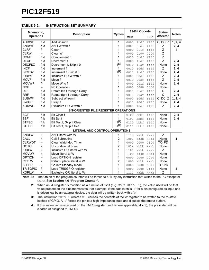
PIC12F519
TABLE 9-2: INSTRUCTION SET SUMMARYMnemonic,Operands Description Cycles
12-Bit Opcode StatusAffected Notes
MSb LSbADDWFANDWFCLRFCLRWCOMFDECFDECFSZINCFINCFSZIORWFMOVFMOVWFNOPRLFRRFSUBWFSWAPFXORWF
f, df, df–f, df, df, df, df, df, df, df–f, df, df, df, df, d
Add W and fAND W with fClear fClear WComplement fDecrement fDecrement f, Skip if 0Increment fIncrement f, Skip if 0Inclusive OR W with fMove fMove W to fNo OperationRotate left f through CarryRotate right f through CarrySubtract W from fSwap fExclusive OR W with f
111111
1(2)
11(2)
111111111
000100010000000000100000001000100011000100100000000000110011000000110001
11df01df011f010001df11df11df10df11df00df00df001f000001df00df10df10df10df
ffffffffffff0000ffffffffffffffffffffffffffffffff0000ffffffffffffffffffff
C, DC, ZZZZZZ
NoneZ
NoneZZ
NoneNone
CC
C, DC, ZNone
Z
1, 2, 42, 4
4
2, 42, 42, 42, 42, 42, 41, 4
2, 42, 4
1, 2, 42, 42, 4
BIT-ORIENTED FILE REGISTER OPERATIONSBCFBSFBTFSCBTFSS
f, bf, bf, bf, b
Bit Clear fBit Set fBit Test f, Skip if ClearBit Test f, Skip if Set
11
1(2)
1(2)
0100010101100111
bbbfbbbfbbbfbbbf
ffffffffffffffff
NoneNoneNoneNone
2, 42, 4
LITERAL AND CONTROL OPERATIONSANDLWCALLCLRWDTGOTOIORLWMOVLWOPTIONRETLWSLEEPTRISGPIOXORLW
kk–kkk–k–fk
AND literal with WCall SubroutineClear Watchdog TimerUnconditional branchInclusive OR literal with WMove literal to WLoad OPTION registerReturn, place literal in WGo into Standby modeLoad TRISGPIO registerExclusive OR literal to W
12121112111
111010010000101k1101110000001000000000001111
kkkkkkkk0000kkkkkkkkkkkk0000kkkk00000000kkkk
kkkkkkkk0100kkkkkkkkkkkk0010kkkk00110fffkkkk
ZNone
TO, PDNone
ZNoneNoneNone
TO, PDNone
Z
1
3
Note 1: The 9th bit of the program counter will be forced to a ‘0’ by any instruction that writes to the PC except for GOTO. See Section 4.6 “Program Counter”.
2: When an I/O register is modified as a function of itself (e.g. MOVF GPIO, 1), the value used will be that value present on the pins themselves. For example, if the data latch is ‘1’ for a pin configured as input and is driven low by an external device, the data will be written back with a ‘0’.
3: The instruction TRIS f, where f = 6, causes the contents of the W register to be written to the tri-state latches of GPIO. A ‘1’ forces the pin to a high-impedance state and disables the output buffers.
4: If this instruction is executed on the TMR0 register (and, where applicable, d = 1), the prescaler will be cleared (if assigned to TMR0).
DS41319B-page 50 © 2008 Microchip Technology Inc.
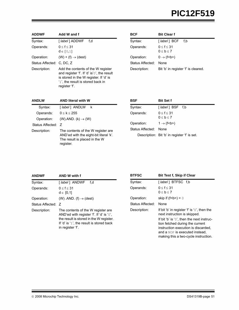
PIC12F519
ADDWF Add W and f
Syntax: [ label ] ADDWF f,d
Operands: 0 ≤ f ≤ 31d ∈ [0,1]
Operation: (W) + (f) → (dest)
Status Affected: C, DC, Z
Description: Add the contents of the W register and register ‘f’. If ‘d’ is’0’, the result is stored in the W register. If ‘d’ is ‘1’, the result is stored back in register ‘f’.
ANDLW AND literal with W
Syntax: [ label ] ANDLW k
Operands: 0 ≤ k ≤ 255
Operation: (W).AND. (k) → (W)
Status Affected: Z
Description: The contents of the W register are AND’ed with the eight-bit literal ‘k’. The result is placed in the W register.
ANDWF AND W with f
Syntax: [ label ] ANDWF f,d
Operands: 0 ≤ f ≤ 31d ∈ [0,1]
Operation: (W) .AND. (f) → (dest)
Status Affected: Z
Description: The contents of the W register are AND’ed with register ‘f’. If ‘d’ is ‘0’, the result is stored in the W register. If ‘d’ is ‘1’, the result is stored back in register ‘f’.
BCF Bit Clear f
Syntax: [ label ] BCF f,b
Operands: 0 ≤ f ≤ 310 ≤ b ≤ 7
Operation: 0 → (f<b>)
Status Affected: None
Description: Bit ‘b’ in register ‘f’ is cleared.
BSF Bit Set f
Syntax: [ label ] BSF f,b
Operands: 0 ≤ f ≤ 310 ≤ b ≤ 7
Operation: 1 → (f<b>)
Status Affected: None
Description: Bit ‘b’ in register ‘f’ is set.
BTFSC Bit Test f, Skip if Clear
Syntax: [ label ] BTFSC f,b
Operands: 0 ≤ f ≤ 310 ≤ b ≤ 7
Operation: skip if (f<b>) = 0
Status Affected: None
Description: If bit ‘b’ in register ‘f’ is ‘0’, then the next instruction is skipped.If bit ‘b’ is ‘0’, then the next instruc-tion fetched during the current instruction execution is discarded, and a NOP is executed instead, making this a two-cycle instruction.
© 2008 Microchip Technology Inc. DS41319B-page 51
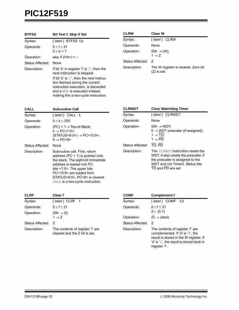
PIC12F519
BTFSS Bit Test f, Skip if Set
Syntax: [ label ] BTFSS f,b
Operands: 0 ≤ f ≤ 310 ≤ b < 7
Operation: skip if (f<b>) = 1
Status Affected: None
Description: If bit ‘b’ in register ‘f’ is ‘1’, then the next instruction is skipped.If bit ‘b’ is ‘1’, then the next instruc-tion fetched during the current instruction execution, is discarded and a NOP is executed instead, making this a two-cycle instruction.
CALL Subroutine CallSyntax: [ label ] CALL k
Operands: 0 ≤ k ≤ 255
Operation: (PC) + 1→ Top-of-Stack;k → PC<7:0>;(STATUS<6:5>) → PC<10:9>;0 → PC<8>
Status Affected: None
Description: Subroutine call. First, return address (PC + 1) is pushed onto the stack. The eight-bit immediate address is loaded into PC bits <7:0>. The upper bits PC<10:9> are loaded from STATUS<6:5>, PC<8> is cleared. CALL is a two-cycle instruction.
CLRF Clear fSyntax: [ label ] CLRF f
Operands: 0 ≤ f ≤ 31
Operation: 00h → (f);1 → Z
Status Affected: Z
Description: The contents of register ‘f’ are cleared and the Z bit is set.
CLRW Clear WSyntax: [ label ] CLRW
Operands: None
Operation: 00h → (W);1 → Z
Status Affected: Z
Description: The W register is cleared. Zero bit (Z) is set.
CLRWDT Clear Watchdog TimerSyntax: [ label ] CLRWDT
Operands: None
Operation: 00h → WDT;0 → WDT prescaler (if assigned);1 → TO;1 → PD
Status Affected: TO, PD
Description: The CLRWDT instruction resets the WDT. It also resets the prescaler, if the prescaler is assigned to the WDT and not Timer0. Status bits TO and PD are set.
COMF Complement fSyntax: [ label ] COMF f,d
Operands: 0 ≤ f ≤ 31d ∈ [0,1]
Operation: (f) → (dest)
Status Affected: Z
Description: The contents of register ‘f’ are complemented. If ‘d’ is ‘0’, the result is stored in the W register. If ‘d’ is ‘1’, the result is stored back in register ‘f’.
DS41319B-page 52 © 2008 Microchip Technology Inc.
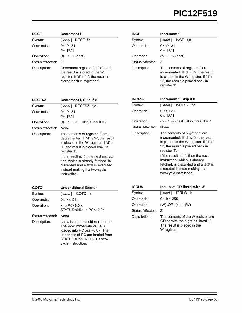
PIC12F519
DECF Decrement fSyntax: [ label ] DECF f,d
Operands: 0 ≤ f ≤ 31d ∈ [0,1]
Operation: (f) – 1 → (dest)
Status Affected: Z
Description: Decrement register ‘f’. If ‘d’ is ‘0’, the result is stored in the W register. If ‘d’ is ‘1’, the result is stored back in register ‘f’.
DECFSZ Decrement f, Skip if 0Syntax: [ label ] DECFSZ f,d
Operands: 0 ≤ f ≤ 31d ∈ [0,1]
Operation: (f) – 1 → d; skip if result = 0
Status Affected: None
Description: The contents of register ‘f’ are decremented. If ‘d’ is ‘0’, the result is placed in the W register. If ‘d’ is ‘1’, the result is placed back in register ‘f’.If the result is ‘0’, the next instruc-tion, which is already fetched, is discarded and a NOP is executed instead making it a two-cycle instruction.
GOTO Unconditional BranchSyntax: [ label ] GOTO k
Operands: 0 ≤ k ≤ 511
Operation: k → PC<8:0>;STATUS<6:5> → PC<10:9>
Status Affected: None
Description: GOTO is an unconditional branch. The 9-bit immediate value is loaded into PC bits <8:0>. The upper bits of PC are loaded from STATUS<6:5>. GOTO is a two-cycle instruction.
INCF Increment fSyntax: [ label ] INCF f,d
Operands: 0 ≤ f ≤ 31d ∈ [0,1]
Operation: (f) + 1 → (dest)
Status Affected: Z
Description: The contents of register ‘f’ are incremented. If ‘d’ is ‘0’, the result is placed in the W register. If ‘d’ is ‘1’, the result is placed back in register ‘f’.
INCFSZ Increment f, Skip if 0Syntax: [ label ] INCFSZ f,d
Operands: 0 ≤ f ≤ 31d ∈ [0,1]
Operation: (f) + 1 → (dest), skip if result = 0
Status Affected: None
Description: The contents of register ‘f’ are incremented. If ‘d’ is ‘0’, the result is placed in the W register. If ‘d’ is ‘1’, the result is placed back in register ‘f’.If the result is ‘0’, then the next instruction, which is already fetched, is discarded and a NOP is executed instead making it a two-cycle instruction.
IORLW Inclusive OR literal with WSyntax: [ label ] IORLW k
Operands: 0 ≤ k ≤ 255
Operation: (W) .OR. (k) → (W)
Status Affected: Z
Description: The contents of the W register are OR’ed with the eight-bit literal ‘k’. The result is placed in the W register.
© 2008 Microchip Technology Inc. DS41319B-page 53
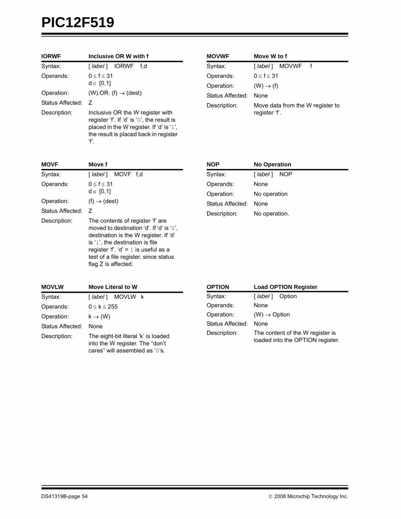
PIC12F519
IORWF Inclusive OR W with fSyntax: [ label ] IORWF f,d
Operands: 0 ≤ f ≤ 31d ∈ [0,1]
Operation: (W).OR. (f) → (dest)
Status Affected: Z
Description: Inclusive OR the W register with register ‘f’. If ‘d’ is ‘0’, the result is placed in the W register. If ‘d’ is ‘1’, the result is placed back in register ‘f’.
MOVF Move fSyntax: [ label ] MOVF f,d
Operands: 0 ≤ f ≤ 31d ∈ [0,1]
Operation: (f) → (dest)
Status Affected: Z
Description: The contents of register ‘f’ are moved to destination ‘d’. If ‘d’ is ‘0’, destination is the W register. If ‘d’ is ‘1’, the destination is file register ‘f’. ‘d’ = 1 is useful as a test of a file register, since status flag Z is affected.
MOVLW Move Literal to WSyntax: [ label ] MOVLW k
Operands: 0 ≤ k ≤ 255
Operation: k → (W)
Status Affected: None
Description: The eight-bit literal ‘k’ is loaded into the W register. The “don’t cares” will assembled as ‘0’s.
MOVWF Move W to fSyntax: [ label ] MOVWF f
Operands: 0 ≤ f ≤ 31
Operation: (W) → (f)
Status Affected: None
Description: Move data from the W register to register ‘f’.
NOP No OperationSyntax: [ label ] NOP
Operands: None
Operation: No operation
Status Affected: None
Description: No operation.
OPTION Load OPTION RegisterSyntax: [ label ] OptionOperands: NoneOperation: (W) → OptionStatus Affected: NoneDescription: The content of the W register is
loaded into the OPTION register.
DS41319B-page 54 © 2008 Microchip Technology Inc.
PIC12F519
RETLW Return with Literal in WSyntax: [ label ] RETLW k
Operands: 0 ≤ k ≤ 255
Operation: k → (W);TOS → PC
Status Affected: None
Description: The W register is loaded with the eight-bit literal ‘k’. The program counter is loaded from the top of the stack (the return address). This is a two-cycle instruction.
RLF Rotate Left f through CarrySyntax: [ label ] RLF f,d
Operands: 0 ≤ f ≤ 31d ∈ [0,1]
Operation: See description below
Status Affected: C
Description: The contents of register ‘f’ are rotated one bit to the left through the Carry flag. If ‘d’ is ‘0’, the result is placed in the W register. If ‘d’ is ‘1’, the result is stored back in reg-ister ‘f’.
RRF Rotate Right f through CarrySyntax: [ label ] RRF f,d
Operands: 0 ≤ f ≤ 31d ∈ [0,1]
Operation: See description below
Status Affected: C
Description: The contents of register ‘f’ are rotated one bit to the right through the Carry flag. If ‘d’ is ‘0’, the result is placed in the W register. If ‘d’ is ‘1’, the result is placed back in register ‘f’.
C register ‘f’
C register ‘f’
SLEEP Enter SLEEP ModeSyntax: [label ] SLEEP
Operands: None
Operation: 00h → WDT;0 → WDT prescaler;1 → TO;0 → PD
Status Affected: TO, PD, GPWUF
Description: Time-out Status bit (TO) is set. The Power-down Status bit (PD) is cleared. GPWUF is unaffected.The WDT and its prescaler are cleared.The processor is put into Sleep mode with the oscillator stopped. See Section 8.8 “Power-down Mode (Sleep)” on Sleep for more details.
SUBWF Subtract W from fSyntax: [label ] SUBWF f,d
Operands: 0 ≤ f ≤ 31d ∈ [0,1]
Operation: (f) – (W) → (dest)
Status Affected: C, DC, Z
Description: Subtract (two’s complement method) the W register from regis-ter ‘f’. If ‘d’ is ‘0’, the result is stored in the W register. If ‘d’ is ‘1’, the result is stored back in register ‘f’.
SWAPF Swap Nibbles in fSyntax: [ label ] SWAPF f,d
Operands: 0 ≤ f ≤ 31d ∈ [0,1]
Operation: (f<3:0>) → (dest<7:4>);(f<7:4>) → (dest<3:0>)
Status Affected: None
Description: The upper and lower nibbles of register ‘f’ are exchanged. If ‘d’ is ‘0’, the result is placed in W register. If ‘d’ is ‘1’, the result is placed in register ‘f’.
© 2008 Microchip Technology Inc. DS41319B-page 55
PIC12F519
TRIS Load TRIS RegisterSyntax: [ label ] TRIS fOperands: f = 6Operation: (W) → TRIS register fStatus Affected: NoneDescription: TRIS register ‘f’ (f = 6 or 7) is
loaded with the contents of the W register.
XORLW Exclusive OR literal with WSyntax: [label ] XORLW k
Operands: 0 ≤ k ≤ 255
Operation: (W) .XOR. k → (W)
Status Affected: Z
Description: The contents of the W register are XOR’ed with the eight-bit literal ‘k’. The result is placed in the W register.
XORWF Exclusive OR W with fSyntax: [ label ] XORWF f,d
Operands: 0 ≤ f ≤ 31d ∈ [0,1]
Operation: (W) .XOR. (f) → (dest)
Status Affected: Z
Description: Exclusive OR the contents of the W register with register ‘f’. If ‘d’ is ‘0’, the result is stored in the W register. If ‘d’ is ‘1’, the result is stored back in register ‘f’.
DS41319B-page 56 © 2008 Microchip Technology Inc.
PIC12F519
10.0 DEVELOPMENT SUPPORTThe PIC® microcontrollers are supported with a fullrange of hardware and software development tools:
• Integrated Development Environment- MPLAB® IDE Software
• Assemblers/Compilers/Linkers- MPASMTM Assembler- MPLAB C18 and MPLAB C30 C Compilers- MPLINKTM Object Linker/
MPLIBTM Object Librarian- MPLAB ASM30 Assembler/Linker/Library
• Simulators- MPLAB SIM Software Simulator
• Emulators- MPLAB ICE 2000 In-Circuit Emulator- MPLAB REAL ICE™ In-Circuit Emulator
• In-Circuit Debugger- MPLAB ICD 2
• Device Programmers- PICSTART® Plus Development Programmer- MPLAB PM3 Device Programmer- PICkit™ 2 Development Programmer
• Low-Cost Demonstration and Development Boards and Evaluation Kits
10.1 MPLAB Integrated Development Environment Software
The MPLAB IDE software brings an ease of softwaredevelopment previously unseen in the 8/16-bit micro-controller market. The MPLAB IDE is a Windows®
operating system-based application that contains:
• A single graphical interface to all debugging tools- Simulator- Programmer (sold separately)- Emulator (sold separately)- In-Circuit Debugger (sold separately)
• A full-featured editor with color-coded context• A multiple project manager• Customizable data windows with direct edit of
contents• High-level source code debugging• Visual device initializer for easy register
initialization• Mouse over variable inspection• Drag and drop variables from source to watch
windows• Extensive on-line help• Integration of select third party tools, such as
HI-TECH Software C Compilers and IAR C Compilers
The MPLAB IDE allows you to:
• Edit your source files (either assembly or C)• One touch assemble (or compile) and download
to PIC MCU emulator and simulator tools (automatically updates all project information)
• Debug using:- Source files (assembly or C)- Mixed assembly and C- Machine code
MPLAB IDE supports multiple debugging tools in asingle development paradigm, from the cost-effectivesimulators, through low-cost in-circuit debuggers, tofull-featured emulators. This eliminates the learningcurve when upgrading to tools with increased flexibilityand power.
© 2008 Microchip Technology Inc. DS41319B-page 57
PIC12F519
10.2 MPASM AssemblerThe MPASM Assembler is a full-featured, universalmacro assembler for all PIC MCUs.The MPASM Assembler generates relocatable objectfiles for the MPLINK Object Linker, Intel® standard HEXfiles, MAP files to detail memory usage and symbolreference, absolute LST files that contain source linesand generated machine code and COFF files fordebugging.
The MPASM Assembler features include:
• Integration into MPLAB IDE projects• User-defined macros to streamline
assembly code• Conditional assembly for multi-purpose
source files• Directives that allow complete control over the
assembly process
10.3 MPLAB C18 and MPLAB C30 C Compilers
The MPLAB C18 and MPLAB C30 Code DevelopmentSystems are complete ANSI C compilers forMicrochip’s PIC18 and PIC24 families of microcon-trollers and the dsPIC30 and dsPIC33 family of digitalsignal controllers. These compilers provide powerfulintegration capabilities, superior code optimization andease of use not found with other compilers.
For easy source level debugging, the compilers providesymbol information that is optimized to the MPLAB IDEdebugger.
10.4 MPLINK Object Linker/MPLIB Object Librarian
The MPLINK Object Linker combines relocatableobjects created by the MPASM Assembler and theMPLAB C18 C Compiler. It can link relocatable objectsfrom precompiled libraries, using directives from alinker script.
The MPLIB Object Librarian manages the creation andmodification of library files of precompiled code. Whena routine from a library is called from a source file, onlythe modules that contain that routine will be linked inwith the application. This allows large libraries to beused efficiently in many different applications.
The object linker/library features include:
• Efficient linking of single libraries instead of many smaller files
• Enhanced code maintainability by grouping related modules together
• Flexible creation of libraries with easy module listing, replacement, deletion and extraction
10.5 MPLAB ASM30 Assembler, Linker and Librarian
MPLAB ASM30 Assembler produces relocatablemachine code from symbolic assembly language fordsPIC30F devices. MPLAB C30 C Compiler uses theassembler to produce its object file. The assemblergenerates relocatable object files that can then bearchived or linked with other relocatable object files andarchives to create an executable file. Notable featuresof the assembler include:
• Support for the entire dsPIC30F instruction set• Support for fixed-point and floating-point data• Command line interface• Rich directive set• Flexible macro language• MPLAB IDE compatibility
10.6 MPLAB SIM Software SimulatorThe MPLAB SIM Software Simulator allows codedevelopment in a PC-hosted environment by simulat-ing the PIC MCUs and dsPIC® DSCs on an instructionlevel. On any given instruction, the data areas can beexamined or modified and stimuli can be applied froma comprehensive stimulus controller. Registers can belogged to files for further run-time analysis. The tracebuffer and logic analyzer display extend the power ofthe simulator to record and track program execution,actions on I/O, most peripherals and internal registers.
The MPLAB SIM Software Simulator fully supportssymbolic debugging using the MPLAB C18 andMPLAB C30 C Compilers, and the MPASM andMPLAB ASM30 Assemblers. The software simulatoroffers the flexibility to develop and debug code outsideof the hardware laboratory environment, making it anexcellent, economical software development tool.
DS41319B-page 58 © 2008 Microchip Technology Inc.
PIC12F519
10.7 MPLAB ICE 2000High-Performance In-Circuit Emulator
The MPLAB ICE 2000 In-Circuit Emulator is intendedto provide the product development engineer with acomplete microcontroller design tool set for PICmicrocontrollers. Software control of the MPLAB ICE2000 In-Circuit Emulator is advanced by the MPLABIntegrated Development Environment, which allowsediting, building, downloading and source debuggingfrom a single environment.
The MPLAB ICE 2000 is a full-featured emulatorsystem with enhanced trace, trigger and data monitor-ing features. Interchangeable processor modules allowthe system to be easily reconfigured for emulation ofdifferent processors. The architecture of the MPLABICE 2000 In-Circuit Emulator allows expansion tosupport new PIC microcontrollers.
The MPLAB ICE 2000 In-Circuit Emulator system hasbeen designed as a real-time emulation system withadvanced features that are typically found on moreexpensive development tools. The PC platform andMicrosoft® Windows® 32-bit operating system werechosen to best make these features available in asimple, unified application.
10.8 MPLAB REAL ICE In-Circuit Emulator System
MPLAB REAL ICE In-Circuit Emulator System isMicrochip’s next generation high-speed emulator forMicrochip Flash DSC® and MCU devices. It debugs andprograms PIC® and dsPIC® Flash microcontrollers withthe easy-to-use, powerful graphical user interface of theMPLAB Integrated Development Environment (IDE),included with each kit.
The MPLAB REAL ICE probe is connected to the designengineer’s PC using a high-speed USB 2.0 interface andis connected to the target with either a connectorcompatible with the popular MPLAB ICD 2 system(RJ11) or with the new high speed, noise tolerant, low-voltage differential signal (LVDS) interconnection(CAT5).
MPLAB REAL ICE is field upgradeable through futurefirmware downloads in MPLAB IDE. In upcomingreleases of MPLAB IDE, new devices will be supported,and new features will be added, such as software break-points and assembly code trace. MPLAB REAL ICEoffers significant advantages over competitive emulatorsincluding low-cost, full-speed emulation, real-timevariable watches, trace analysis, complex breakpoints, aruggedized probe interface and long (up to three meters)interconnection cables.
10.9 MPLAB ICD 2 In-Circuit DebuggerMicrochip’s In-Circuit Debugger, MPLAB ICD 2, is apowerful, low-cost, run-time development tool,connecting to the host PC via an RS-232 or high-speedUSB interface. This tool is based on the Flash PICMCUs and can be used to develop for these and otherPIC MCUs and dsPIC DSCs. The MPLAB ICD 2 utilizesthe in-circuit debugging capability built into the Flashdevices. This feature, along with Microchip’s In-CircuitSerial ProgrammingTM (ICSPTM) protocol, offers cost-effective, in-circuit Flash debugging from the graphicaluser interface of the MPLAB Integrated DevelopmentEnvironment. This enables a designer to develop anddebug source code by setting breakpoints, single step-ping and watching variables, and CPU status andperipheral registers. Running at full speed enablestesting hardware and applications in real time. MPLABICD 2 also serves as a development programmer forselected PIC devices.
10.10 MPLAB PM3 Device ProgrammerThe MPLAB PM3 Device Programmer is a universal,CE compliant device programmer with programmablevoltage verification at VDDMIN and VDDMAX formaximum reliability. It features a large LCD display(128 x 64) for menus and error messages and a modu-lar, detachable socket assembly to support variouspackage types. The ICSP™ cable assembly is includedas a standard item. In Stand-Alone mode, the MPLABPM3 Device Programmer can read, verify and programPIC devices without a PC connection. It can also setcode protection in this mode. The MPLAB PM3connects to the host PC via an RS-232 or USB cable.The MPLAB PM3 has high-speed communications andoptimized algorithms for quick programming of largememory devices and incorporates an SD/MMC card forfile storage and secure data applications.
© 2008 Microchip Technology Inc. DS41319B-page 59
PIC12F519
10.11 PICSTART Plus DevelopmentProgrammerThe PICSTART Plus Development Programmer is aneasy-to-use, low-cost, prototype programmer. Itconnects to the PC via a COM (RS-232) port. MPLABIntegrated Development Environment software makesusing the programmer simple and efficient. ThePICSTART Plus Development Programmer supportsmost PIC devices in DIP packages up to 40 pins.Larger pin count devices, such as the PIC16C92X andPIC17C76X, may be supported with an adapter socket.The PICSTART Plus Development Programmer is CEcompliant.
10.12 PICkit 2 Development ProgrammerThe PICkit™ 2 Development Programmer is a low-costprogrammer and selected Flash device debugger withan easy-to-use interface for programming many ofMicrochip’s baseline, mid-range and PIC18F families ofFlash memory microcontrollers. The PICkit 2 Starter Kitincludes a prototyping development board, twelvesequential lessons, software and HI-TECH’s PICC™Lite C compiler, and is designed to help get up to speedquickly using PIC® microcontrollers. The kit provideseverything needed to program, evaluate and developapplications using Microchip’s powerful, mid-rangeFlash memory family of microcontrollers.
10.13 Demonstration, Development and Evaluation Boards
A wide variety of demonstration, development andevaluation boards for various PIC MCUs and dsPICDSCs allows quick application development on fully func-tional systems. Most boards include prototyping areas foradding custom circuitry and provide application firmwareand source code for examination and modification.
The boards support a variety of features, including LEDs,temperature sensors, switches, speakers, RS-232interfaces, LCD displays, potentiometers and additionalEEPROM memory.
The demonstration and development boards can beused in teaching environments, for prototyping customcircuits and for learning about various microcontrollerapplications.
In addition to the PICDEM™ and dsPICDEM™ demon-stration/development board series of circuits, Microchiphas a line of evaluation kits and demonstration softwarefor analog filter design, KEELOQ® security ICs, CAN,IrDA®, PowerSmart battery management, SEEVAL®
evaluation system, Sigma-Delta ADC, flow ratesensing, plus many more.
Check the Microchip web page (www.microchip.com)and the latest “Product Selector Guide” (DS00148) forthe complete list of demonstration, development andevaluation kits.
DS41319B-page 60 © 2008 Microchip Technology Inc.

PIC12F519
11.0 ELECTRICAL CHARACTERISTICS
Absolute Maximum Ratings(†)
Ambient temperature under bias.......................................................................................................... -40°C to +125°C
Storage temperature ............................................................................................................................ -65°C to +150°C
Voltage on VDD with respect to VSS ...............................................................................................................0 to +6.5V
Voltage on MCLR with respect to VSS..........................................................................................................0 to +13.5V
Voltage on all other pins with respect to VSS ............................................................................... -0.3V to (VDD + 0.3V)
Total power dissipation(1) ..................................................................................................................................700 mW
Max. current out of VSS pin ................................................................................................................................200 mA
Max. current into VDD pin ...................................................................................................................................150 mA
Input clamp current, IIK (VI < 0 or VI > VDD) ...................................................................................................................±20 mA
Output clamp current, IOK (VO < 0 or VO > VDD) ...........................................................................................................±20 mA
Max. output current sunk by any I/O pin .............................................................................................................. 25 mA
Max. output current sourced by any I/O pin ......................................................................................................... 25 mA
Max. output current sourced by I/O port .............................................................................................................. 75 mA
Max. output current sunk by I/O port ................................................................................................................... 75 mA
Note 1: Power dissipation is calculated as follows: PDIS = VDD x {IDD – ∑ IOH} + ∑ {(VDD – VOH) x IOH} + ∑(VOL x IOL) †NOTICE: Stresses above those listed under “Absolute Maximum Ratings” may cause permanent damage to thedevice. This is a stress rating only and functional operation of the device at those or any other conditions above thoseindicated in the operation listings of this specification is not implied. Exposure to maximum rating conditions forextended periods may affect device reliability.
© 2008 Microchip Technology Inc. DS41319B-page 61
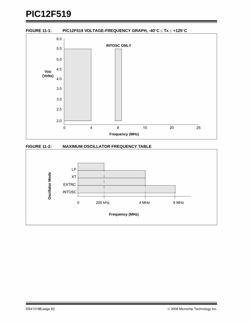
PIC12F519
FIGURE 11-1: PIC12F519 VOLTAGE-FREQUENCY GRAPH, -40°C ≤ TA ≤ +125°CFIGURE 11-2: MAXIMUM OSCILLATOR FREQUENCY TABLE
6.0
2.5
4.0
3.0
0
3.5
4.5
5.0
5.5
4 10
Frequency (MHz)
VDD
20
(Volts)
25
2.0
8
INTOSC ONLY
0 200 kHz 4 MHz
Frequency (MHz)
8 MHz
LP
XT
EXTRC
INTOSC
Osc
illat
or M
ode
DS41319B-page 62 © 2008 Microchip Technology Inc.
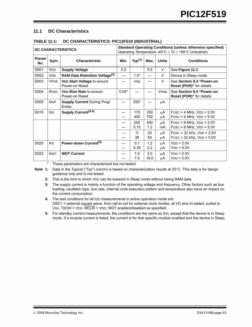
PIC12F519
11.1 DC CharacteristicsTABLE 11-1: DC CHARACTERISTICS: PIC12F519 (INDUSTRIAL)
DC CHARACTERISTICS Standard Operating Conditions (unless otherwise specified)Operating Temperature -40°C ≤ TA ≤ +85°C (industrial)
Param No. Sym. Characteristic Min. Typ(1) Max. Units Conditions
D001 VDD Supply Voltage 2.0 5.5 V See Figure 11-1 D002 VDR RAM Data Retention Voltage(2) — 1.5* — V Device in Sleep modeD003 VPOR VDD Start Voltage to ensure
Power-on Reset— Vss — V See Section 8.4 “Power-on
Reset (POR)” for detailsD004 SVDD VDD Rise Rate to ensure
Power-on Reset0.05* — — V/ms See Section 8.4 “Power-on
Reset (POR)” for detailsD005 IDDP Supply Current During Prog/
Erase.— 250* — μA
D010 IDD Supply Current(3,4) ——
175400
250700
μAμA
FOSC = 4 MHz, VDD = 2.0VFOSC = 4 MHz, VDD = 5.0V
——
2500.75
4001.2
μAmA
FOSC = 8 MHz, VDD = 2.0VFOSC = 8 MHz, VDD = 5.0V
——
1138
2054
μAμA
FOSC = 32 kHz, VDD = 2.0VFOSC = 32 kHz, VDD = 5.0V
D020 IPD Power-down Current(5) ——
0.10.35
1.22.2
μAμA
VDD = 2.0VVDD = 5.0V
D022 IWDT WDT Current ——
1.07.0
3.016.0
μAμA
VDD = 2.0VVDD = 5.0V
* These parameters are characterized but not tested.Note 1: Data in the Typical (“Typ”) column is based on characterization results at 25°C. This data is for design
guidance only and is not tested.2: This is the limit to which VDD can be lowered in Sleep mode without losing RAM data.3: The supply current is mainly a function of the operating voltage and frequency. Other factors such as bus
loading, oscillator type, bus rate, internal code execution pattern and temperature also have an impact on the current consumption.
4: The test conditions for all IDD measurements in active operation mode are:OSC1 = external square wave, from rail-to-rail for external clock modes; all I/O pins tri-stated, pulled to VSS, T0CKI = VDD, MCLR = VDD; WDT enabled/disabled as specified.
5: For standby current measurements, the conditions are the same as IDD, except that the device is in Sleep mode. If a module current is listed, the current is for that specific module enabled and the device in Sleep.
© 2008 Microchip Technology Inc. DS41319B-page 63
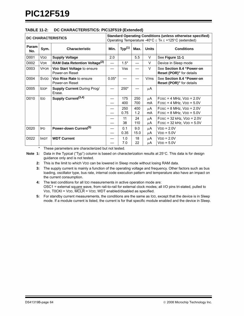
PIC12F519
TABLE 11-2: DC CHARACTERISTICS: PIC12F519 (Extended)DC CHARACTERISTICS Standard Operating Conditions (unless otherwise specified)Operating Temperature -40°C ≤ TA ≤ +125°C (extended)
Param No. Sym. Characteristic Min. Typ(1) Max. Units Conditions
D001 VDD Supply Voltage 2.0 5.5 V See Figure 11-1 D002 VDR RAM Data Retention Voltage(2) — 1.5* — V Device in Sleep modeD003 VPOR VDD Start Voltage to ensure
Power-on Reset— Vss — V See Section 8.4 “Power-on
Reset (POR)” for detailsD004 SVDD VDD Rise Rate to ensure
Power-on Reset0.05* — — V/ms See Section 8.4 “Power-on
Reset (POR)” for detailsD005 IDDP Supply Current During Prog/
Erase.— 250* — μA
D010 IDD Supply Current(3,4) ——
175400
250700
μAmA
FOSC = 4 MHz, VDD = 2.0VFOSC = 4 MHz, VDD = 5.0V
——
2500.75
4001.2
μAmA
FOSC = 8 MHz, VDD = 2.0VFOSC = 8 MHz, VDD = 5.0V
——
1138
24110
μAμA
FOSC = 32 kHz, VDD = 2.0VFOSC = 32 kHz, VDD = 5.0V
D020 IPD Power-down Current(5) ——
0.10.35
9.015.0
μAμA
VDD = 2.0VVDD = 5.0V
D022 IWDT WDT Current ——
1.07.0
1822
μAμA
VDD = 2.0VVDD = 5.0V
* These parameters are characterized but not tested.Note 1: Data in the Typical (“Typ”) column is based on characterization results at 25°C. This data is for design
guidance only and is not tested.2: This is the limit to which VDD can be lowered in Sleep mode without losing RAM data.3: The supply current is mainly a function of the operating voltage and frequency. Other factors such as bus
loading, oscillator type, bus rate, internal code execution pattern and temperature also have an impact on the current consumption.
4: The test conditions for all IDD measurements in active operation mode are:OSC1 = external square wave, from rail-to-rail for external clock modes; all I/O pins tri-stated, pulled to VSS, T0CKI = VDD, MCLR = VDD; WDT enabled/disabled as specified.
5: For standby current measurements, the conditions are the same as IDD, except that the device is in Sleep mode. If a module current is listed, the current is for that specific module enabled and the device in Sleep.
DS41319B-page 64 © 2008 Microchip Technology Inc.
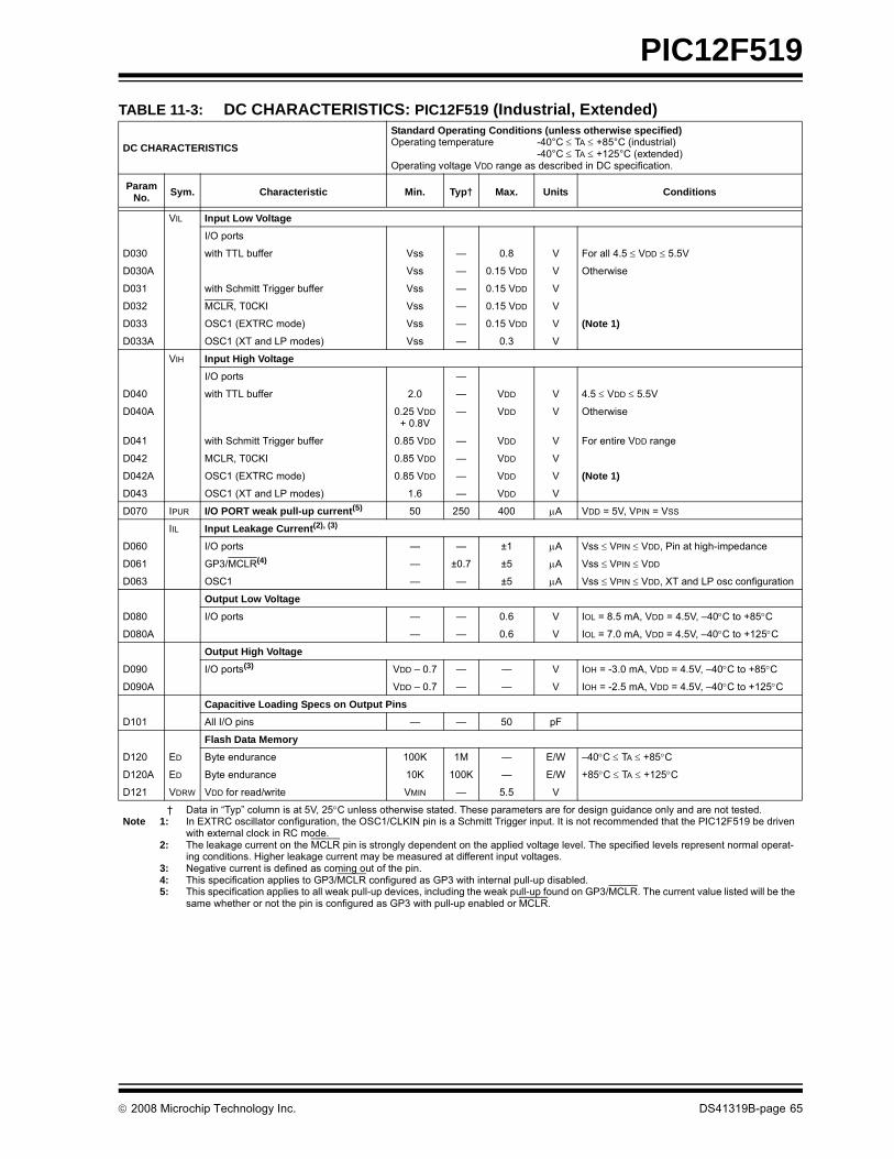
PIC12F519
TABLE 11-3: DC CHARACTERISTICS: PIC12F519 (Industrial, Extended)DC CHARACTERISTICSStandard Operating Conditions (unless otherwise specified)Operating temperature -40°C ≤ TA ≤ +85°C (industrial)
-40°C ≤ TA ≤ +125°C (extended)Operating voltage VDD range as described in DC specification.
ParamNo. Sym. Characteristic Min. Typ† Max. Units Conditions
VIL Input Low VoltageI/O ports
D030 with TTL buffer Vss — 0.8 V For all 4.5 ≤ VDD ≤ 5.5V
D030A Vss — 0.15 VDD V Otherwise
D031 with Schmitt Trigger buffer Vss — 0.15 VDD V
D032 MCLR, T0CKI Vss — 0.15 VDD V
D033 OSC1 (EXTRC mode) Vss — 0.15 VDD V (Note 1)D033A OSC1 (XT and LP modes) Vss — 0.3 V
VIH Input High VoltageI/O ports —
D040 with TTL buffer 2.0 — VDD V 4.5 ≤ VDD ≤ 5.5V
D040A 0.25 VDD+ 0.8V
— VDD V Otherwise
D041 with Schmitt Trigger buffer 0.85 VDD — VDD V For entire VDD range
D042 MCLR, T0CKI 0.85 VDD — VDD V
D042A OSC1 (EXTRC mode) 0.85 VDD — VDD V (Note 1)D043 OSC1 (XT and LP modes) 1.6 — VDD V
D070 IPUR I/O PORT weak pull-up current(5) 50 250 400 μA VDD = 5V, VPIN = VSS
IIL Input Leakage Current(2), (3)
D060 I/O ports — — ±1 μA Vss ≤ VPIN ≤ VDD, Pin at high-impedance
D061 GP3/MCLR(4) — ±0.7 ±5 μA Vss ≤ VPIN ≤ VDD
D063 OSC1 — — ±5 μA Vss ≤ VPIN ≤ VDD, XT and LP osc configuration
Output Low VoltageD080 I/O ports — — 0.6 V IOL = 8.5 mA, VDD = 4.5V, –40°C to +85°C
D080A — — 0.6 V IOL = 7.0 mA, VDD = 4.5V, –40°C to +125°C
Output High VoltageD090 I/O ports(3) VDD – 0.7 — — V IOH = -3.0 mA, VDD = 4.5V, –40°C to +85°C
D090A VDD – 0.7 — — V IOH = -2.5 mA, VDD = 4.5V, –40°C to +125°C
Capacitive Loading Specs on Output PinsD101 All I/O pins — — 50 pF
Flash Data MemoryD120 ED Byte endurance 100K 1M — E/W –40°C ≤ TA ≤ +85°C
D120A ED Byte endurance 10K 100K — E/W +85°C ≤ TA ≤ +125°C
D121 VDRW VDD for read/write VMIN — 5.5 V
† Data in “Typ” column is at 5V, 25°C unless otherwise stated. These parameters are for design guidance only and are not tested.Note 1: In EXTRC oscillator configuration, the OSC1/CLKIN pin is a Schmitt Trigger input. It is not recommended that the PIC12F519 be driven
with external clock in RC mode.2: The leakage current on the MCLR pin is strongly dependent on the applied voltage level. The specified levels represent normal operat-
ing conditions. Higher leakage current may be measured at different input voltages.3: Negative current is defined as coming out of the pin.4: This specification applies to GP3/MCLR configured as GP3 with internal pull-up disabled.5: This specification applies to all weak pull-up devices, including the weak pull-up found on GP3/MCLR. The current value listed will be the
same whether or not the pin is configured as GP3 with pull-up enabled or MCLR.
© 2008 Microchip Technology Inc. DS41319B-page 65
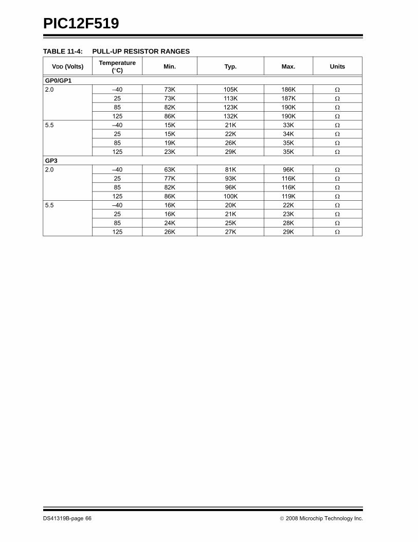
PIC12F519
TABLE 11-4: PULL-UP RESISTOR RANGESVDD (Volts) Temperature (°C) Min. Typ. Max. Units
GP0/GP12.0 –40 73K 105K 186K Ω
25 73K 113K 187K Ω85 82K 123K 190K Ω
125 86K 132K 190K Ω5.5 –40 15K 21K 33K Ω
25 15K 22K 34K Ω85 19K 26K 35K Ω
125 23K 29K 35K ΩGP32.0 –40 63K 81K 96K Ω
25 77K 93K 116K Ω85 82K 96K 116K Ω
125 86K 100K 119K Ω5.5 –40 16K 20K 22K Ω
25 16K 21K 23K Ω85 24K 25K 28K Ω
125 26K 27K 29K Ω
DS41319B-page 66 © 2008 Microchip Technology Inc.
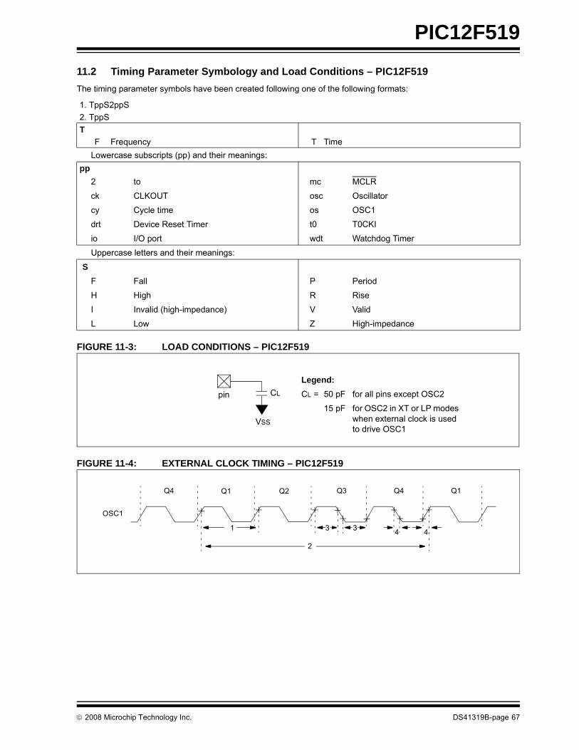
PIC12F519
11.2 Timing Parameter Symbology and Load Conditions – PIC12F519The timing parameter symbols have been created following one of the following formats:FIGURE 11-3: LOAD CONDITIONS – PIC12F519
FIGURE 11-4: EXTERNAL CLOCK TIMING – PIC12F519
1. TppS2ppS2. TppST
F Frequency T TimeLowercase subscripts (pp) and their meanings:
pp2 to mc MCLR
ck CLKOUT osc Oscillator
cy Cycle time os OSC1
drt Device Reset Timer t0 T0CKI
io I/O port wdt Watchdog Timer
Uppercase letters and their meanings:
SF Fall P Period
H High R Rise
I Invalid (high-impedance) V Valid
L Low Z High-impedance
CL
VSS
pin
Legend:CL = 50 pF for all pins except OSC2
15 pF for OSC2 in XT or LP modes when external clock is used to drive OSC1
OSC1
Q4 Q1 Q2 Q3 Q4 Q1
1 3 3 4 4
2
© 2008 Microchip Technology Inc. DS41319B-page 67
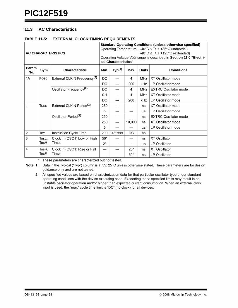
PIC12F519
11.3 AC CharacteristicsTABLE 11-5: EXTERNAL CLOCK TIMING REQUIREMENTS
AC CHARACTERISTICS
Standard Operating Conditions (unless otherwise specified)Operating Temperature -40°C ≤ TA ≤ +85°C (industrial),
-40°C ≤ TA ≤ +125°C (extended)Operating Voltage VDD range is described in Section 11.0 “Electri-cal Characteristics”
Param No. Sym. Characteristic Min. Typ(1) Max. Units Conditions
1A FOSC External CLKIN Frequency(2) DC — 4 MHz XT Oscillator modeDC — 200 kHz LP Oscillator mode
Oscillator Frequency(2) DC — 4 MHz EXTRC Oscillator mode 0.1 — 4 MHz XT Oscillator mode DC — 200 kHz LP Oscillator mode
1 TOSC External CLKIN Period(2) 250 — — ns XT Oscillator mode5 — — μs LP Oscillator mode
Oscillator Period(2) 250 — — ns EXTRC Oscillator mode 250 — 10,000 ns XT Oscillator mode
5 — — μs LP Oscillator mode2 TCY Instruction Cycle Time 200 4/FOSC DC ns3 TosL,
TosHClock in (OSC1) Low or High Time
50* — — ns XT Oscillator2* — — μs LP Oscillator
4 TosR, TosF
Clock in (OSC1) Rise or Fall Time
— — 25* ns XT Oscillator— — 50* ns LP Oscillator
* These parameters are characterized but not tested.Note 1: Data in the Typical (“Typ”) column is at 5V, 25°C unless otherwise stated. These parameters are for design
guidance only and are not tested.2: All specified values are based on characterization data for that particular oscillator type under standard
operating conditions with the device executing code. Exceeding these specified limits may result in an unstable oscillator operation and/or higher than expected current consumption. When an external clock input is used, the “max” cycle time limit is “DC” (no clock) for all devices.
DS41319B-page 68 © 2008 Microchip Technology Inc.
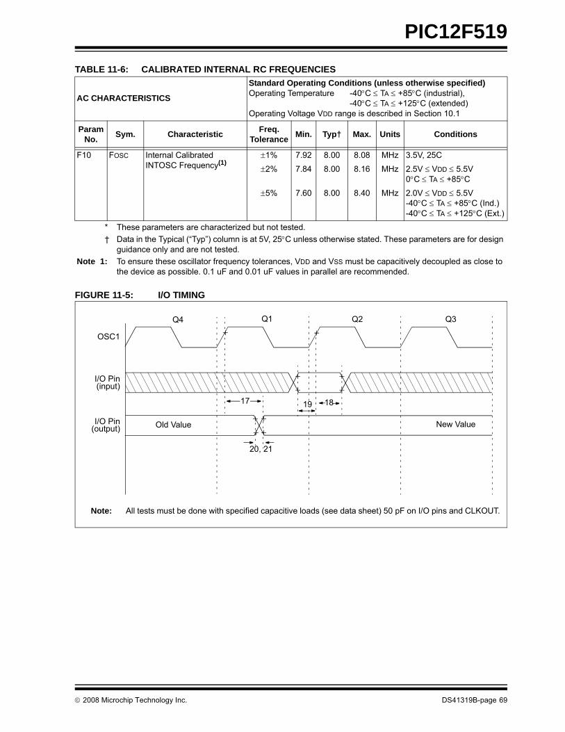
PIC12F519
TABLE 11-6: CALIBRATED INTERNAL RC FREQUENCIESFIGURE 11-5: I/O TIMING
AC CHARACTERISTICS
Standard Operating Conditions (unless otherwise specified)Operating Temperature -40°C ≤ TA ≤ +85°C (industrial),
-40°C ≤ TA ≤ +125°C (extended)Operating Voltage VDD range is described in Section 10.1
Param No. Sym. Characteristic Freq.
Tolerance Min. Typ† Max. Units Conditions
F10 FOSC Internal Calibrated INTOSC Frequency(1)
±1% 7.92 8.00 8.08 MHz 3.5V, 25C
±2% 7.84 8.00 8.16 MHz 2.5V ≤ VDD ≤ 5.5V0°C ≤ TA ≤ +85°C
±5% 7.60 8.00 8.40 MHz 2.0V ≤ VDD ≤ 5.5V-40°C ≤ TA ≤ +85°C (Ind.)-40°C ≤ TA ≤ +125°C (Ext.)
* These parameters are characterized but not tested.† Data in the Typical (“Typ”) column is at 5V, 25°C unless otherwise stated. These parameters are for design
guidance only and are not tested.Note 1: To ensure these oscillator frequency tolerances, VDD and VSS must be capacitively decoupled as close to
the device as possible. 0.1 uF and 0.01 uF values in parallel are recommended.
OSC1
I/O Pin(input)
I/O Pin(output)
Q4 Q1 Q2 Q3
17
20, 21
18
Old Value New Value
19
Note: All tests must be done with specified capacitive loads (see data sheet) 50 pF on I/O pins and CLKOUT.
© 2008 Microchip Technology Inc. DS41319B-page 69
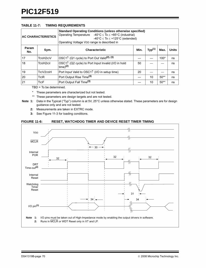
PIC12F519
TABLE 11-7: TIMING REQUIREMENTSFIGURE 11-6: RESET, WATCHDOG TIMER AND DEVICE RESET TIMER TIMING
AC CHARACTERISTICS
Standard Operating Conditions (unless otherwise specified)Operating Temperature -40°C ≤ TA ≤ +85°C (industrial)
-40°C ≤ TA ≤ +125°C (extended)Operating Voltage VDD range is described in
Param No. Sym. Characteristic Min. Typ(1) Max. Units
17 TOSH2IOV OSC1↑ (Q1 cycle) to Port Out Valid(2), (3) — — 100* ns
18 TOSH2IOI OSC1↑ (Q2 cycle) to Port Input Invalid (I/O in hold time)(2)
50 — — ns
19 TIOV2OSH Port Input Valid to OSC1↑ (I/O in setup time) 20 — — ns
20 TIOR Port Output Rise Time(3) — 10 50** ns
21 TIOF Port Output Fall Time(3) — 10 50** ns
TBD = To be determined.
* These parameters are characterized but not tested.** These parameters are design targets and are not tested.
Note 1: Data in the Typical (“Typ”) column is at 5V, 25°C unless otherwise stated. These parameters are for design guidance only and are not tested.
2: Measurements are taken in EXTRC mode.3: See Figure 11-3 for loading conditions.
VDD
MCLR
InternalPOR
DRTTime-out(2)
InternalReset
WatchdogTimerReset
32
31
34
I/O pin(1)
32 32
34
30
Note 1: I/O pins must be taken out of High-Impedance mode by enabling the output drivers in software.2: Runs in MCLR or WDT Reset only in XT and LP.
DS41319B-page 70 © 2008 Microchip Technology Inc.
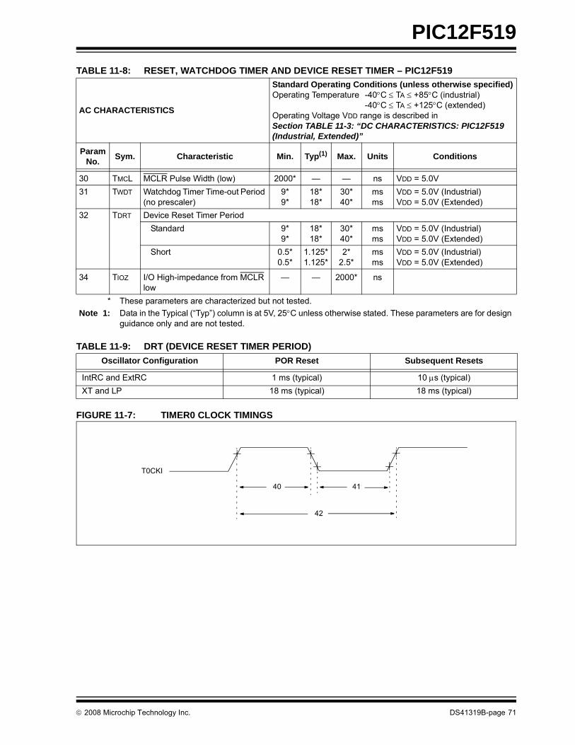
PIC12F519
TABLE 11-8: RESET, WATCHDOG TIMER AND DEVICE RESET TIMER – PIC12F519TABLE 11-9: DRT (DEVICE RESET TIMER PERIOD)
FIGURE 11-7: TIMER0 CLOCK TIMINGS
AC CHARACTERISTICS
Standard Operating Conditions (unless otherwise specified)Operating Temperature -40°C ≤ TA ≤ +85°C (industrial)
-40°C ≤ TA ≤ +125°C (extended)Operating Voltage VDD range is described inSection TABLE 11-3: “DC CHARACTERISTICS: PIC12F519 (Industrial, Extended)”
ParamNo. Sym. Characteristic Min. Typ(1) Max. Units Conditions
30 TMCL MCLR Pulse Width (low) 2000* — — ns VDD = 5.0V31 TWDT Watchdog Timer Time-out Period
(no prescaler) 9*9*
18*18*
30*40*
msms
VDD = 5.0V (Industrial)VDD = 5.0V (Extended)
32 TDRT Device Reset Timer PeriodStandard 9*
9*18*18*
30*40*
msms
VDD = 5.0V (Industrial)VDD = 5.0V (Extended)
Short 0.5*0.5*
1.125*1.125*
2*2.5*
msms
VDD = 5.0V (Industrial)VDD = 5.0V (Extended)
34 TIOZ I/O High-impedance from MCLR low
— — 2000* ns
* These parameters are characterized but not tested.Note 1: Data in the Typical (“Typ”) column is at 5V, 25°C unless otherwise stated. These parameters are for design
guidance only and are not tested.
Oscillator Configuration POR Reset Subsequent Resets
IntRC and ExtRC 1 ms (typical) 10 μs (typical)XT and LP 18 ms (typical) 18 ms (typical)
T0CKI
40 41
42
© 2008 Microchip Technology Inc. DS41319B-page 71
PIC12F519
TABLE 11-10: TIMER0 CLOCK REQUIREMENTSTABLE 11-11: FLASH DATA MEMORY WRITE/ERASE REQUIREMENTS
AC CHARACTERISTICS
Standard Operating Conditions (unless otherwise specified)Operating Temperature -40°C ≤ TA ≤ +85°C (industrial)
-40°C ≤ TA ≤ +125°C (extended)Operating Voltage VDD range is described inSection TABLE 11-3: “DC CHARACTERISTICS: PIC12F519 (Industrial, Extended)”
Param No. Sym. Characteristic Min. Typ(1) Max. Units Conditions
40 Tt0H T0CKI High Pulse Width
No Prescaler 0.5 TCY + 20* — — nsWith Prescaler 10* — — ns
41 Tt0L T0CKI Low Pulse Width
No Prescaler 0.5 TCY + 20* — — nsWith Prescaler 10* — — ns
42 Tt0P T0CKI Period 20 or TCY + 40* N — — ns Whichever is greater.N = Prescale Value(1, 2, 4,..., 256)
* These parameters are characterized but not tested.Note 1: Data in the Typical (“Typ”) column is at 5V, 25°C unless otherwise stated. These parameters are for design
guidance only and are not tested.
AC CHARACTERISTICS
Standard Operating Conditions (unless otherwise specified)Operating Temperature -40°C ≤ TA ≤ +85°C (industrial)
-40°C ≤ TA ≤ +125°C (extended)Operating Voltage VDD range is described inSection TABLE 11-3: “DC CHARACTERISTICS: PIC12F519 (Industrial, Extended)”
Param No. Sym. Characteristic Min. Typ(1) Max. Units Conditions
43 TDW Flash Data Memory Write Cycle Time
2 3.5 5 ms
44 TDE Flash Data Memory Erase Cycle Time
2 3 4 ms
* These parameters are characterized but not tested.Note 1: Data in the Typical (“Typ”) column is at 5V, 25°C unless otherwise stated. These parameters are for design
guidance only and are not tested.
DS41319B-page 72 © 2008 Microchip Technology Inc.
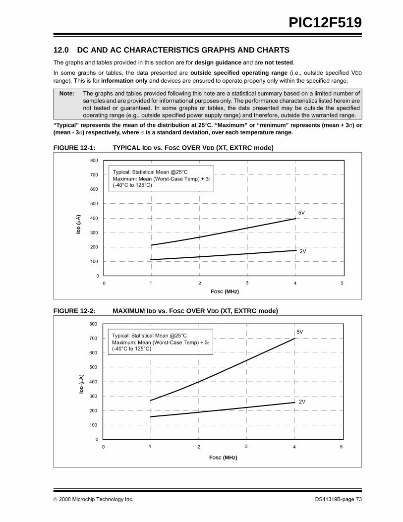
PIC12F519
12.0 DC AND AC CHARACTERISTICS GRAPHS AND CHARTSThe graphs and tables provided in this section are for design guidance and are not tested.
In some graphs or tables, the data presented are outside specified operating range (i.e., outside specified VDD
range). This is for information only and devices are ensured to operate properly only within the specified range.
“Typical” represents the mean of the distribution at 25°C. “Maximum” or “minimum” represents (mean + 3σ) or(mean - 3σ) respectively, where σ is a standard deviation, over each temperature range.
FIGURE 12-1: TYPICAL IDD vs. FOSC OVER VDD (XT, EXTRC mode)
FIGURE 12-2: MAXIMUM IDD vs. FOSC OVER VDD (XT, EXTRC mode)
Note: The graphs and tables provided following this note are a statistical summary based on a limited number ofsamples and are provided for informational purposes only. The performance characteristics listed herein arenot tested or guaranteed. In some graphs or tables, the data presented may be outside the specifiedoperating range (e.g., outside specified power supply range) and therefore, outside the warranted range.
FOSC (MHz)
0
100
200
300
400
500
600
700
800
Typical: Statistical Mean @25°CMaximum: Mean (Worst-Case Temp) + 3σ(-40°C to 125°C)
0 2 431 5
2V
5V
IDD
(μA
)
FOSC (MHz)
0
100
200
300
400
500
600
700
800
Typical: Statistical Mean @25°CMaximum: Mean (Worst-Case Temp) + 3σ(-40°C to 125°C)
0 2 431 5
2V
5V
IDD
(μA
)
© 2008 Microchip Technology Inc. DS41319B-page 73
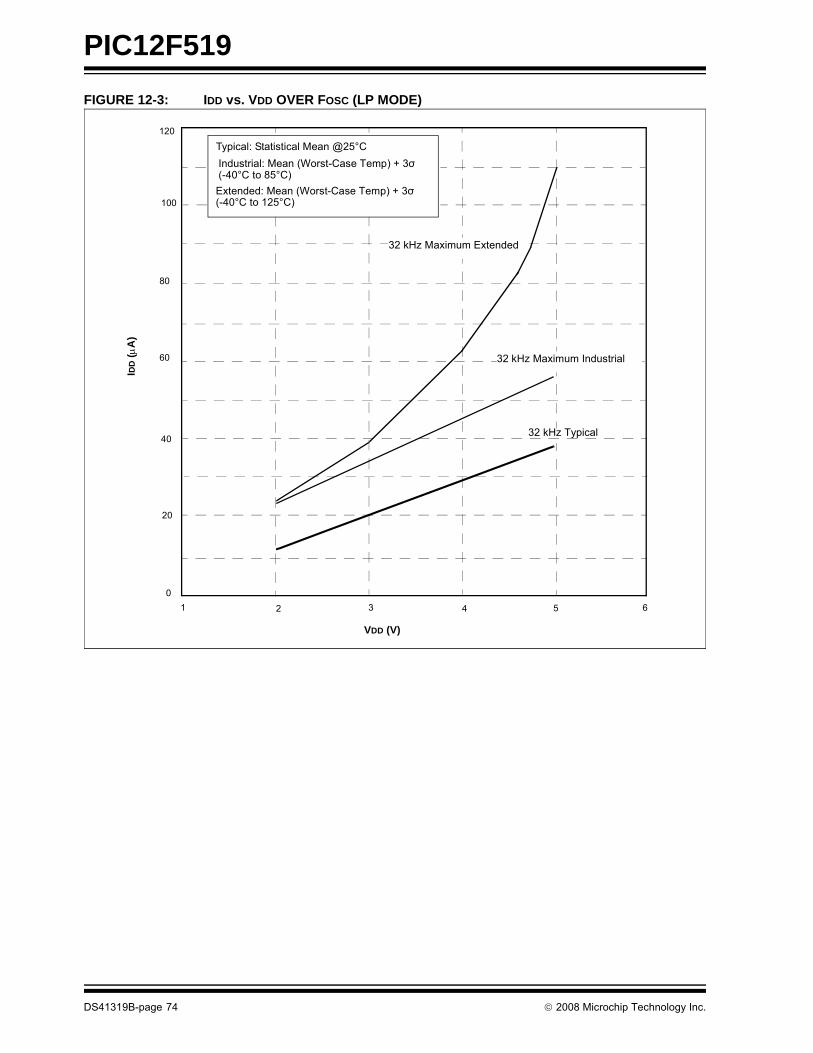
PIC12F519
FIGURE 12-3: IDD vs. VDD OVER FOSC (LP MODE)40
60
80
100
VDD (V)
IDD
(μA
)
2 431 5
120
Typical: Statistical Mean @25°C
Extended: Mean (Worst-Case Temp) + 3σ(-40°C to 125°C)
32 kHz Maximum Industrial
32 kHz Typical
20
06
32 kHz Maximum Extended
Industrial: Mean (Worst-Case Temp) + 3σ (-40°C to 85°C)
DS41319B-page 74 © 2008 Microchip Technology Inc.
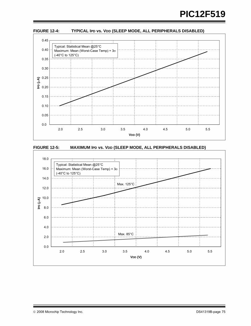
PIC12F519
FIGURE 12-4: TYPICAL IPD vs. VDD (SLEEP MODE, ALL PERIPHERALS DISABLED)FIGURE 12-5: MAXIMUM IPD vs. VDD (SLEEP MODE, ALL PERIPHERALS DISABLED)
0.0
0.05
0.10
0.15
0.20
0.25
0.30
0.35
0.40
0.45
2.0 2.5 3.0 3.5 4.0 4.5 5.0 5.5
VDD (V)
IPD
(μA
)
Typical: Statistical Mean @25°CMaximum: Mean (Worst-Case Temp) + 3σ(-40°C to 125°C)
Max. 125°C
Max. 85°C
0.0
2.0
4.0
6.0
8.0
10.0
12.0
14.0
16.0
18.0
2.0 2.5 3.0 3.5 4.0 4.5 5.0 5.5
VDD (V)
IPD
(μA
)
Typical: Statistical Mean @25°CMaximum: Mean (Worst-Case Temp) + 3σ(-40°C to 125°C)
© 2008 Microchip Technology Inc. DS41319B-page 75
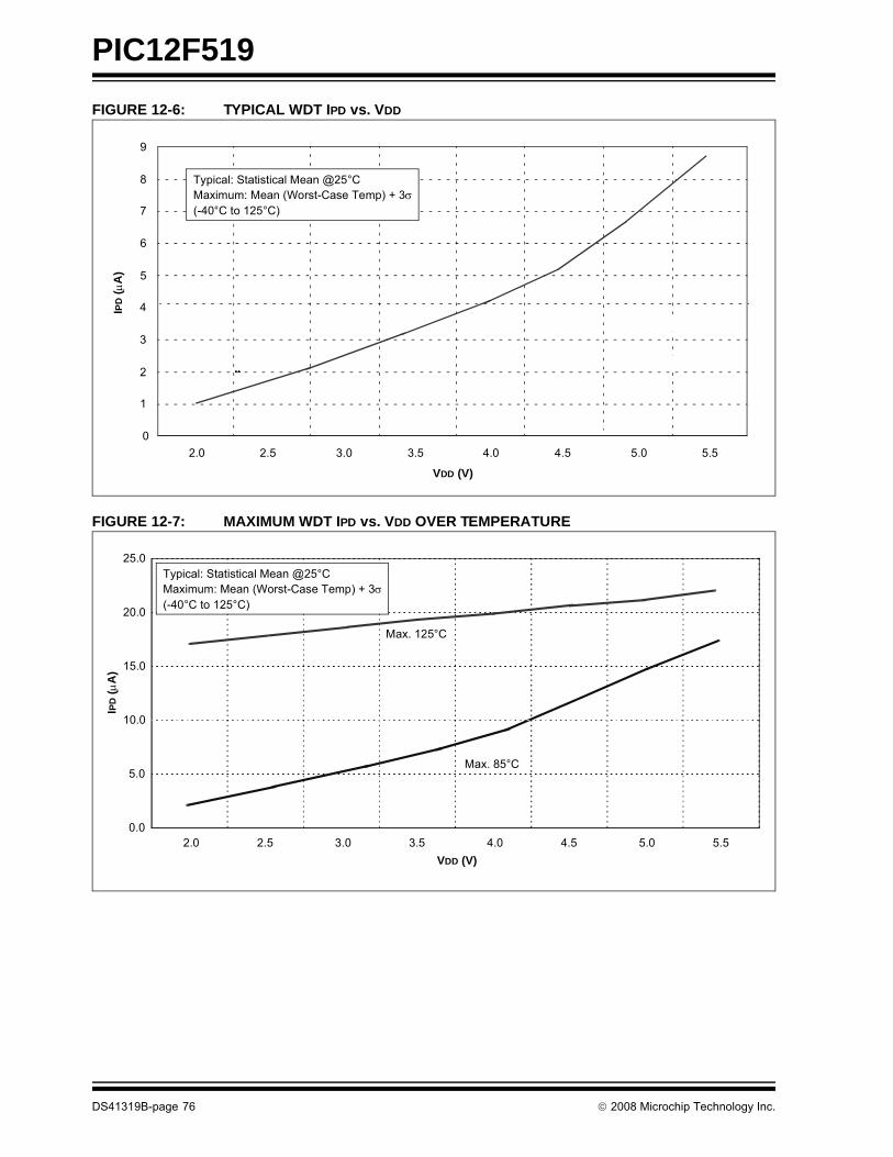
PIC12F519
FIGURE 12-6: TYPICAL WDT IPD vs. VDDFIGURE 12-7: MAXIMUM WDT IPD vs. VDD OVER TEMPERATURE
0
1
2
3
4
5
6
7
8
9
2.0 2.5 3.0 3.5 4.0 4.5 5.0 5.5
VDD (V)
IPD
(μA
)
Typical: Statistical Mean @25°CMaximum: Mean (Worst-Case Temp) + 3σ(-40°C to 125°C)
Max. 125°C
Max. 85°C
0.0
5.0
10.0
15.0
20.0
25.0
2.0 2.5 3.0 3.5 4.0 4.5 5.0 5.5VDD (V)
IPD
(μA
)
Typical: Statistical Mean @25°CMaximum: Mean (Worst-Case Temp) + 3σ(-40°C to 125°C)
DS41319B-page 76 © 2008 Microchip Technology Inc.
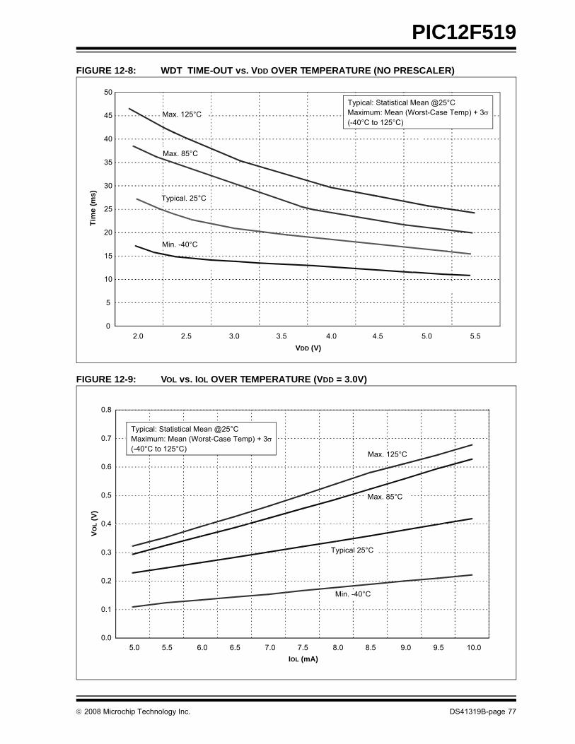
PIC12F519
FIGURE 12-8: WDT TIME-OUT vs. VDD OVER TEMPERATURE (NO PRESCALER)FIGURE 12-9: VOL vs. IOL OVER TEMPERATURE (VDD = 3.0V)
0
5
10
15
20
25
30
35
40
45
50
2.0 2.5 3.0 3.5 4.0 4.5 5.0 5.5VDD (V)
Tim
e (m
s)Typical: Statistical Mean @25°CMaximum: Mean (Worst-Case Temp) + 3σ(-40°C to 125°C)
Max. 125°C
Max. 85°C
Typical. 25°C
Min. -40°C
0.0
0.1
0.2
0.3
0.4
0.5
0.6
0.7
0.8
5.0 5.5 6.0 6.5 7.0 7.5 8.0 8.5 9.0 9.5 10.0IOL (mA)
VOL
(V)
Max. 85°C
Max. 125°C
Typical 25°C
Min. -40°C
Typical: Statistical Mean @25°CMaximum: Mean (Worst-Case Temp) + 3σ(-40°C to 125°C)
© 2008 Microchip Technology Inc. DS41319B-page 77
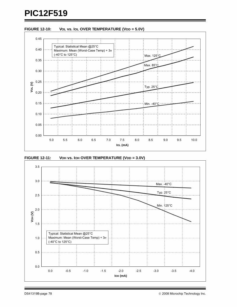
PIC12F519
FIGURE 12-10: VOL vs. IOL OVER TEMPERATURE (VDD = 5.0V)FIGURE 12-11: VOH vs. IOH OVER TEMPERATURE (VDD = 3.0V)
0.00
0.05
0.10
0.15
0.20
0.25
0.30
0.35
0.40
0.45
5.0 5.5 6.0 6.5 7.0 7.5 8.0 8.5 9.0 9.5 10.0
IOL (mA)
VOL
(V)
Typical: Statistical Mean @25×CMaximum: Meas + 3 (-40×C to 125×C)
Typical: Statistical Mean @25°CMaximum: Mean (Worst-Case Temp) + 3σ(-40°C to 125°C)
Max. 85°C
Typ. 25°C
Min. -40°C
Max. 125°C
0.0
0.5
1.0
1.5
2.0
2.5
3.0
3.5
-4.0-3.5-3.0-2.5-2.0-1.5-1.0-0.50.0IOH (mA)
VOH
(V)
Typ. 25°C
Max. -40°C
Min. 125°C
Typical: Statistical Mean @25°CMaximum: Mean (Worst-Case Temp) + 3σ(-40°C to 125°C)
DS41319B-page 78 © 2008 Microchip Technology Inc.
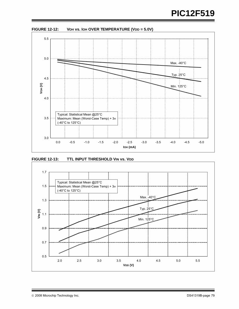
PIC12F519
FIGURE 12-12: VOH vs. IOH OVER TEMPERATURE (VDD = 5.0V)FIGURE 12-13: TTL INPUT THRESHOLD VIN vs. VDD
3.0
3.5
4.0
4.5
5.0
5.5
-5.0-4.5-4.0-3.5-3.0-2.5-2.0-1.5-1.0-0.50.0IOH (mA)
VOH
(V)
Max. -40°C
Typ. 25°C
Min. 125°C
Typical: Statistical Mean @25°CMaximum: Mean (Worst-Case Temp) + 3σ(-40°C to 125°C)
0.5
0.7
0.9
1.1
1.3
1.5
1.7
2.0 2.5 3.0 3.5 4.0 4.5 5.0 5.5VDD (V)
VIN
(V) Typ. 25°C
Max. -40°C
Min. 125°C
Typical: Statistical Mean @25°CMaximum: Mean (Worst-Case Temp) + 3σ(-40°C to 125°C)
© 2008 Microchip Technology Inc. DS41319B-page 79
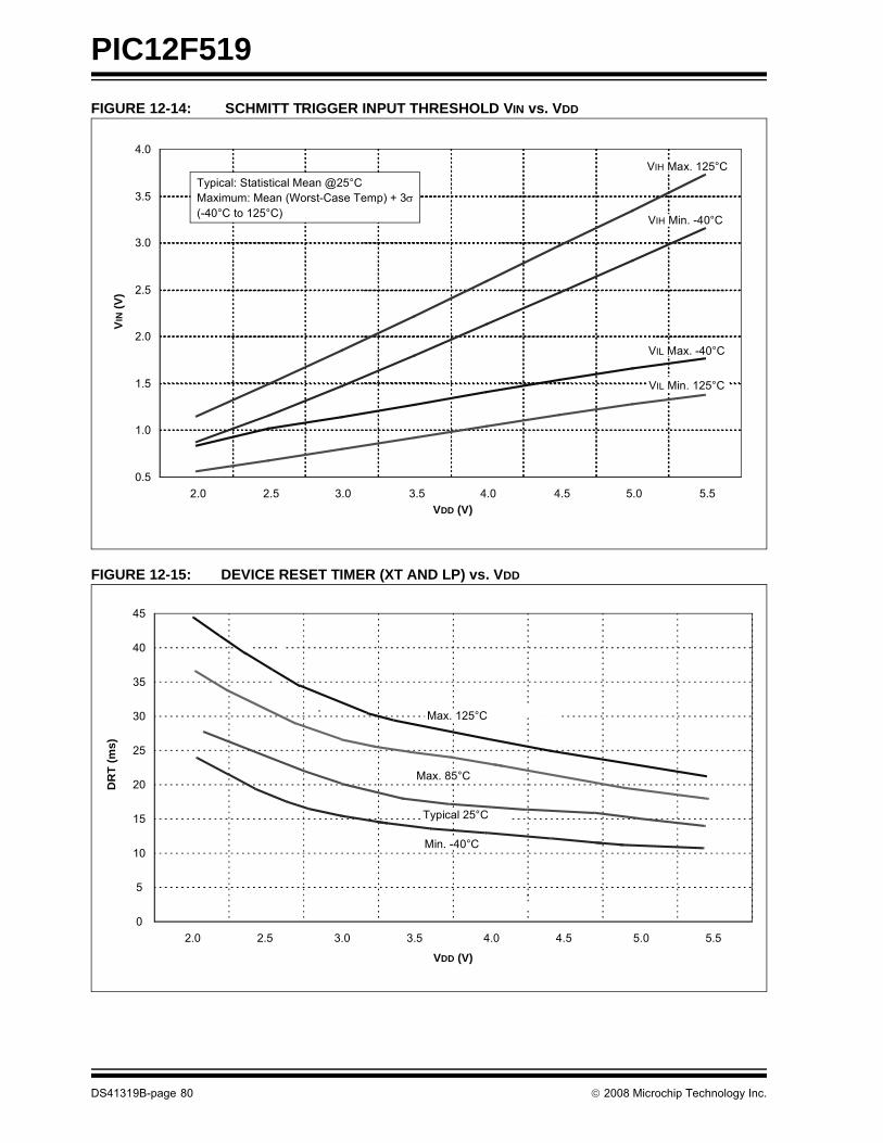
PIC12F519
FIGURE 12-14: SCHMITT TRIGGER INPUT THRESHOLD VIN vs. VDDFIGURE 12-15: DEVICE RESET TIMER (XT AND LP) vs. VDD
0.5
1.0
1.5
2.0
2.5
3.0
3.5
4.0
2.0 2.5 3.0 3.5 4.0 4.5 5.0 5.5VDD (V)
VIN
(V)
VIH Max. 125°C
VIH Min. -40°C
VIL Min. 125°C
VIL Max. -40°C
Typical: Statistical Mean @25°CMaximum: Mean (Worst-Case Temp) + 3σ(-40°C to 125°C)
0
5
10
15
20
25
30
35
40
45
2.0 2.5 3.0 3.5 4.0 4.5 5.0 5.5
VDD (V)
DR
T (m
s)
Min. -40°C
Max. 125°C
Typical 25°C
Max. 85°C
DS41319B-page 80 © 2008 Microchip Technology Inc.
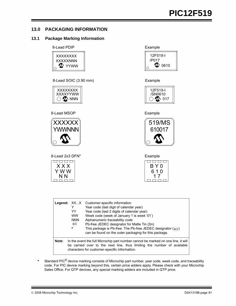
PIC12F519
13.0 PACKAGING INFORMATION
13.1 Package Marking Information
XXXXXNNN
8-Lead PDIP
XXXXXXXX
YYWW/P017
Example
12F519-I
0610
8-Lead SOIC (3.90 mm)
XXXXXXXXXXXXYYWW
NNN
Example
12F519-I/SN0610
017
8-Lead MSOP
XXXXXXYWWNNN
Example
519/MS610017
X X XY W W
N N
8-Lead 2x3 DFN*
B Y 06 1 01 7
Example
* Standard PIC® device marking consists of Microchip part number, year code, week code, and traceabilitycode. For PIC device marking beyond this, certain price adders apply. Please check with your MicrochipSales Office. For QTP devices, any special marking adders are included in QTP price.
Legend: XX...X Customer-specific informationY Year code (last digit of calendar year)YY Year code (last 2 digits of calendar year)WW Week code (week of January 1 is week ‘01’)NNN Alphanumeric traceability code Pb-free JEDEC designator for Matte Tin (Sn)* This package is Pb-free. The Pb-free JEDEC designator ( )
can be found on the outer packaging for this package.
Note: In the event the full Microchip part number cannot be marked on one line, it willbe carried over to the next line, thus limiting the number of availablecharacters for customer-specific information.
3e
3e
© 2008 Microchip Technology Inc. DS41319B-page 81
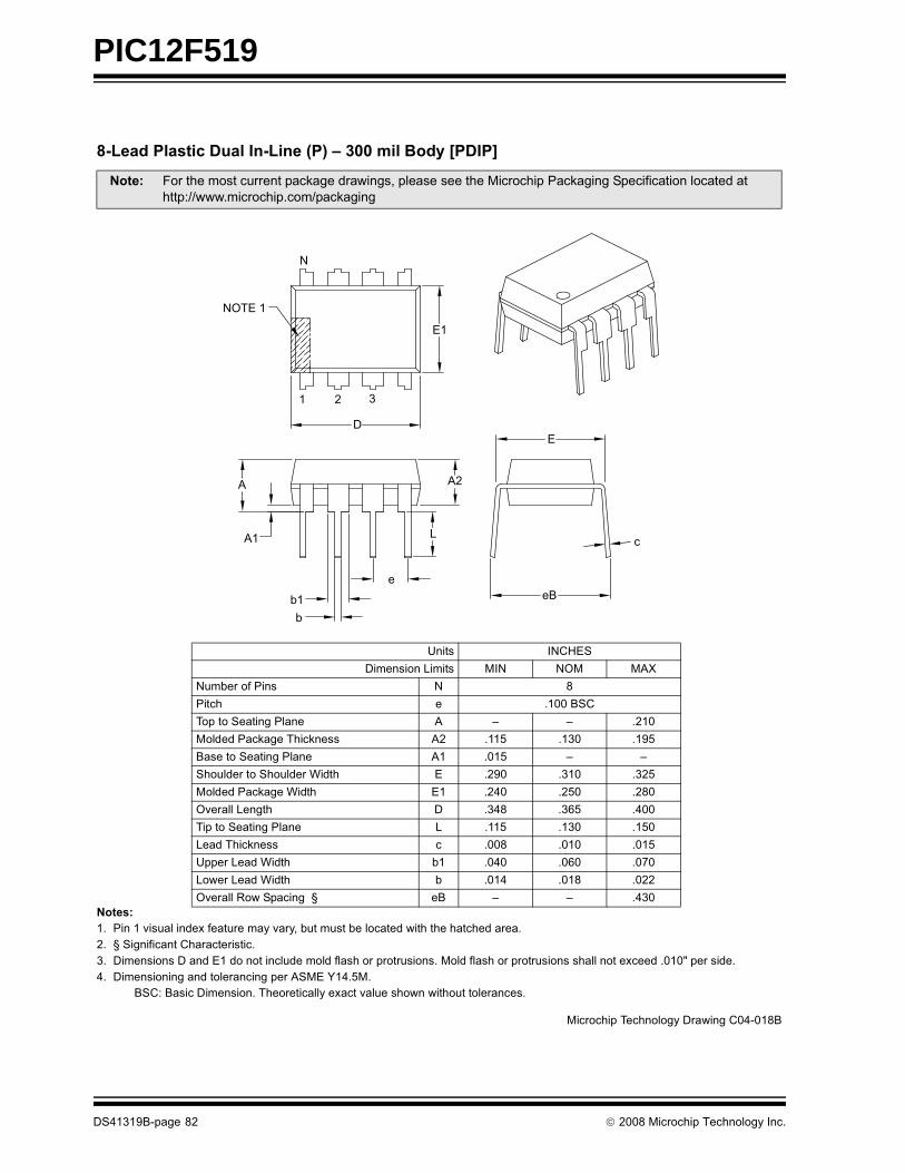
PIC12F519
���������� ���������� ������������� ����������
�������� ������ �!"�����#�$�%��&"��'��� ��(�)"&�'"!&�)�����&�#�*�&��&�����&���#������� +������%����&�,����&��!&���-� ��'��!��!�����#�.��#��&�����"#��'�#�%��!����&"!��!����#�%��!����&"!��!�!������&��$���#�����/����!�#���� ��'��!��������#�&���������������.�0������
1�,2�1�!�����'��!���� ���&��������$��&� ��"��!�*��*�&�"&�&������!�
����� 3�&���'!&��"��&����4����#�*���!(�����!��!���&��������������4�����������%���&������&�#��&��&&�255***�'��������'5���4�����
6��&! �7,8.���'��!���9�'�&! ��7 7:� ��;
7"')��%����! 7 <��&�� � �����1�, ��&����&��������� � = = ������#�#����4���� ���4��!! �� ���� ��-� ����1�!��&����&��������� �� ���� = =��"�#��&���"�#��>�#&� . ���� �-�� �-����#�#����4����>�#&� .� ���� ���� ��<�: �����9���&� � �-�< �-?� ���� ���&����&��������� 9 ���� ��-� ����9��#� ���4��!! � ���< ���� ����6����9��#�>�#&� )� ���� ��?� ����9*��9��#�>�#&� ) ���� ���< ����: ������*����������+ �1 = = ��-�
N
E1
NOTE 1
D
1 2 3
A
A1
A2
L
b1b
e
E
eB
c
������� ������� ��*��� ,�����<1
DS41319B-page 82 © 2008 Microchip Technology Inc.
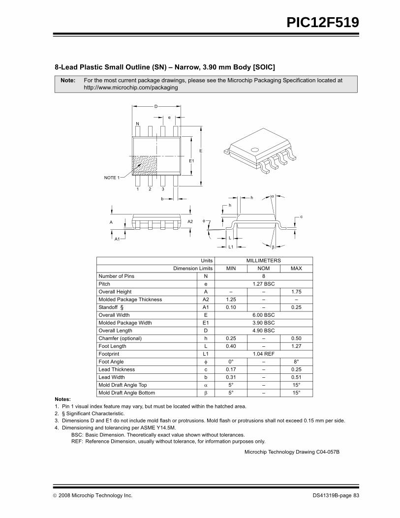
PIC12F519
���������� �� ���!�� ���� �������""�#$��%&����������� !�'�
�������� ������ �!"�����#�$�%��&"��'��� ��(�)"&�'"!&�)�����&�#�*�&����&�����&���#������� +������%����&�,����&��!&���-� ��'��!��!�����#�.��#��&�����"#��'�#�%��!����&"!��!����#�%��!����&"!��!�!������&��$���#������''����!�#���� ��'��!��������#�&���������������.�0������
1�,2 1�!�����'��!���� ���&��������$��&� ��"��!�*��*�&�"&�&������!��.32 ��%��������'��!��(�"!"�����*�&�"&�&������(�%���%'�&����"�!�!�����
����� 3�&���'!&��"��&����4����#�*���!(�����!��!���&��������������4�����������%���&������&�#��&��&&�255***�'��������'5���4�����
6��&! ��99��. .����'��!���9�'�&! ��7 7:� ��;
7"')��%����! 7 <��&�� � �����1�,: �����8����& � = = ������#�#����4���� ���4��!! �� ���� = =�&��#%%��+ �� ���� = ����: �����>�#&� . ?����1�,��#�#����4����>�#&� .� -����1�,: �����9���&� � �����1�,,��'%��@�&����A � ���� = ����3&�9���&� 9 ���� = ����3&���& 9� ������.33&������ � �B = <B9��#� ���4��!! � ���� = ����9��#�>�#&� ) ��-� = ������#���%&������� � � �B = ��B��#���%&�������1&&' � �B = ��B
D
Ne
E
E1
NOTE 1
1 2 3
b
A
A1
A2
L
L1
c
h
h
φ
β
α
������� ������� ��*��� ,������1
© 2008 Microchip Technology Inc. DS41319B-page 83
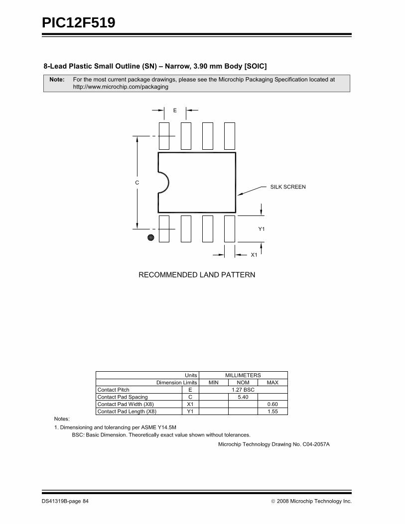
PIC12F519
���������� �� ���!�� ���� �������""�#$��%&����������� !�'�
����� 3�&���'!&��"��&����4����#�*���!(�����!��!���&��������������4�����������%���&������&�#��&��&&�255***�'��������'5���4�����
DS41319B-page 84 © 2008 Microchip Technology Inc.
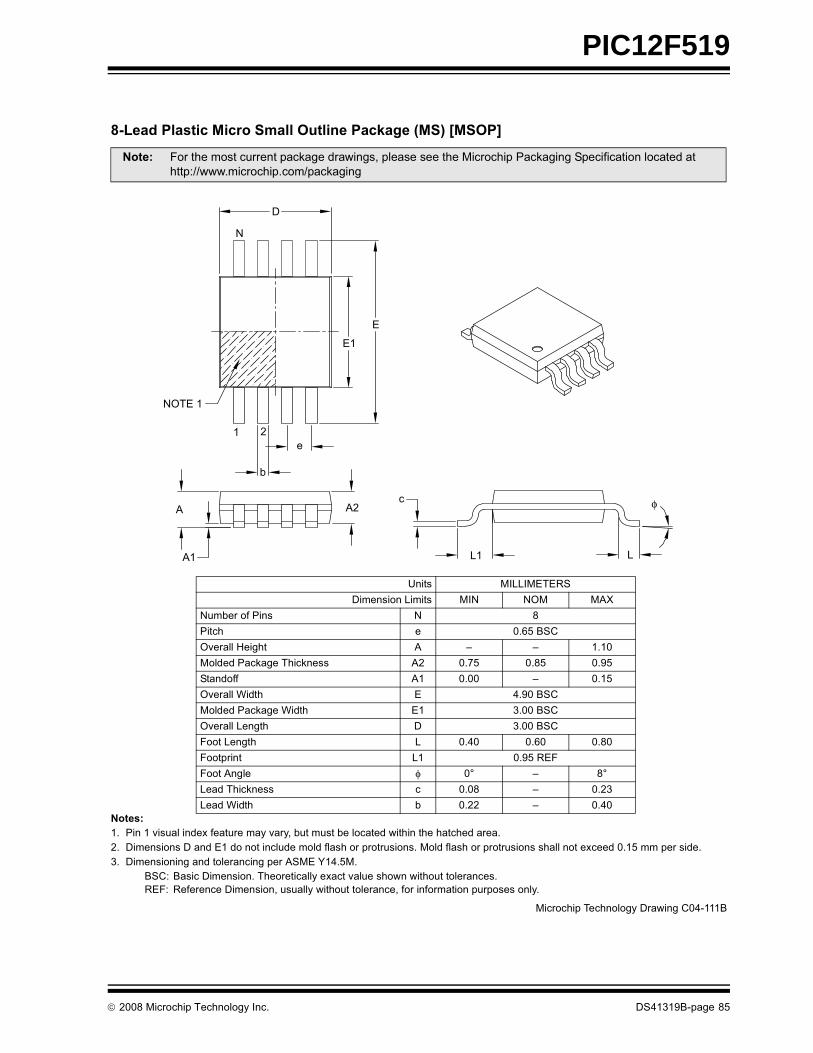
PIC12F519
���������� ��( �"�� ���!�� �����)�*���( ���( !�
�������� ������ �!"�����#�$�%��&"��'��� ��(�)"&�'"!&�)�����&�#�*�&����&�����&���#������� ��'��!��!�����#�.��#��&�����"#��'�#�%��!����&"!��!����#�%��!����&"!��!�!������&��$���#������''����!�#��-� ��'��!��������#�&���������������.�0������
1�,2 1�!�����'��!���� ���&��������$��&� ��"��!�*��*�&�"&�&������!��.32 ��%��������'��!��(�"!"�����*�&�"&�&������(�%���%'�&����"�!�!�����
����� 3�&���'!&��"��&����4����#�*���!(�����!��!���&��������������4�����������%���&������&�#��&��&&�255***�'��������'5���4�����
6��&! ��99��. .����'��!���9�'�&! ��7 7:� ��;
7"')��%����! 7 <��&�� � ��?��1�,: �����8����& � = = ������#�#����4���� ���4��!! �� ���� ��<� �����&��#%%� �� ���� = ����: �����>�#&� . �����1�,��#�#����4����>�#&� .� -����1�,: �����9���&� � -����1�,3&�9���&� 9 ���� ��?� ��<�3&���& 9� ������.33&������ � �B = <B9��#� ���4��!! � ���< = ���-9��#�>�#&� ) ���� = ����
D
N
E
E1
NOTE 1
1 2e
b
A
A1
A2c
L1 L
φ
������� ������� ��*��� ,������1
© 2008 Microchip Technology Inc. DS41319B-page 85
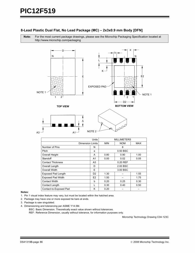
PIC12F519
���������� ������+��$�����������)�*���('����,-�-�%&�����������+��
�������� ������ �!"�����#�$�%��&"��'��� ��(�)"&�'"!&�)�����&�#�*�&����&�����&���#������� ���4����'����� ������'���$�!�#�&���)�!��&���#!�-� ���4�����!�!�*�!���"��&�#��� ��'��!��������#�&���������������.�0������
1�,2 1�!�����'��!���� ���&��������$��&� ��"��!�*��*�&�"&�&������!��.32 ��%��������'��!��(�"!"�����*�&�"&�&������(�%���%'�&����"�!�!�����
����� 3�&���'!&��"��&����4����#�*���!(�����!��!���&��������������4�����������%���&������&�#��&��&&�255***�'��������'5���4�����
6��&! ��99��. .����'��!���9�'�&! ��7 7:� ��;
7"')��%����! 7 <��&�� � �����1�,: �����8����& � ��<� ���� �����&��#%%� �� ���� ���� ����,�&��&� ���4��!! �- ������.3: �����9���&� � �����1�,: �����>�#&� . -����1�,.$�!�#���#�9���&� �� ��-� = ����.$�!�#���#�>�#&� .� ���� = ����,�&��&�>�#&� ) ���� ���� ��-�,�&��&�9���&� 9 ��-� ���� ����,�&��&�&�.$�!�#���# C ���� = =
D
N
E
NOTE 1
1 2
EXPOSED PAD
NOTE 12 1
D2
K
L
E2
N
eb
A3 A1
A
NOTE 2
BOTTOM VIEWTOP VIEW
������� ������� ��*��� ,�����-,
DS41319B-page 86 © 2008 Microchip Technology Inc.
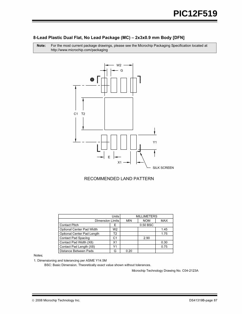
PIC12F519
���������� ������+��$�����������)�*���('����,-�-�%&�����������+��
����� 3�&���'!&��"��&����4����#�*���!(�����!��!���&��������������4�����������%���&������&�#��&��&&�255***�'��������'5���4�����
© 2008 Microchip Technology Inc. DS41319B-page 87
PIC12F519
APPENDIX A: REVISION HISTORYRevision A (May 2007)Original release of this document.
Revision B (September 2008)Added DC and AC Characteristics graphs; UpdatedElectrical Characteristics section; Updated PackageDrawings and made general edits.
DS41319B-page 88 © 2008 Microchip Technology Inc.
PIC12F519
INDEXAALU ....................................................................................... 9Assembler
MPASM Assembler..................................................... 58
BBlock Diagram
On-Chip Reset Circuit ................................................. 43Timer0......................................................................... 31TMR0/WDT Prescaler................................................. 35Watchdog Timer.......................................................... 46
CC Compilers
MPLAB C18 ................................................................ 58MPLAB C30 ................................................................ 58
Carry ..................................................................................... 9Clocking Scheme ................................................................ 12Code Protection ............................................................ 37, 48CONFIG1 Register.............................................................. 38Configuration Bits................................................................ 37Customer Change Notification Service ............................... 91Customer Notification Service............................................. 91Customer Support ............................................................... 91
DDC and AC Characteristics ................................................. 73
Graphs and Tables ..................................................... 73Development Support ......................................................... 57Digit Carry ............................................................................. 9
EErrata .................................................................................... 3
FFSR..................................................................................... 20FSR Register ...................................................................... 20Fuses. See Configuration Bits
GGPIO ................................................................................... 23
II/O Interfacing ..................................................................... 25I/O Port................................................................................ 23I/O Ports .............................................................................. 23I/O Programming Considerations........................................ 30ID Locations .................................................................. 37, 48INDF.................................................................................... 20INDF Register ..................................................................... 20Indirect Data Addressing..................................................... 20Instruction Cycle ................................................................. 12Instruction Flow/Pipelining .................................................. 12Instruction Set Summary..................................................... 50Internet Address.................................................................. 91
LLoading of PC ..................................................................... 19
MMemory Map
PIC12F519 ................................................................. 13Memory Organization ......................................................... 13
Data EEPROM Memory ............................................. 21Program Memory (PIC12F519) .................................. 13
Microchip Internet Web Site................................................ 91MPLAB ASM30 Assembler, Linker, Librarian ..................... 58MPLAB ICD 2 In-Circuit Debugger ..................................... 59MPLAB ICE 2000 High-Performance Universal
In-Circuit Emulator...................................................... 59MPLAB Integrated Development Environment Software.... 57MPLAB PM3 Device Programmer ...................................... 59MPLAB REAL ICE In-Circuit Emulator System .................. 59MPLINK Object Linker/MPLIB Object Librarian .................. 58
OOPTION Register................................................................ 17OSC selection..................................................................... 37OSCCAL Register............................................................... 18Oscillator Configurations..................................................... 39Oscillator Types
HS............................................................................... 39LP ............................................................................... 39RC .............................................................................. 39XT ............................................................................... 39
PPIC12F519 Device Varieties................................................. 7PICSTART Plus Development Programmer....................... 60POR
Device Reset Timer (DRT) ................................... 37, 45PD............................................................................... 47TO............................................................................... 47
Power-down Mode.............................................................. 47Prescaler ............................................................................ 34Program Counter ................................................................ 19
QQ cycles .............................................................................. 12
RRC Oscillator....................................................................... 40Reader Response............................................................... 92Read-Modify-Write.............................................................. 30Register File Map
PIC16C57/CR57......................................................... 14Registers
CONFIG1 (Configuration Word Register 1)................ 38Special Function ......................................................... 14
Reset .................................................................................. 37
SSleep ............................................................................ 37, 47Software Simulator (MPLAB SIM) ...................................... 58Special Features of the CPU .............................................. 37Special Function Registers ................................................. 14Stack................................................................................... 19STATUS Register ........................................................... 9, 16
© 2008 Microchip Technology Inc. DS41319B-page 89
PIC12F519
TTimer0Timer0 (TMR0) Module ............................................... 31TMR0 with External Clock........................................... 33
Timing Diagrams and Specifications................................... 67Timing Parameter Symbology and Load Conditions........... 67TRIS Registers.................................................................... 23
WWake-up from Sleep ........................................................... 47Watchdog Timer (WDT) ................................................ 37, 45
Period.......................................................................... 45Programming Considerations ..................................... 45
WWW Address.................................................................... 91WWW, On-Line Support........................................................ 3
ZZero bit .................................................................................. 9
DS41319B-page 90 © 2008 Microchip Technology Inc.
PIC12F519
THE MICROCHIP WEB SITEMicrochip provides online support via our WWW site atwww.microchip.com. This web site is used as a meansto make files and information easily available tocustomers. Accessible by using your favorite Internetbrowser, the web site contains the followinginformation:
• Product Support – Data sheets and errata, application notes and sample programs, design resources, user’s guides and hardware support documents, latest software releases and archived software
• General Technical Support – Frequently Asked Questions (FAQ), technical support requests, online discussion groups, Microchip consultant program member listing
• Business of Microchip – Product selector and ordering guides, latest Microchip press releases, listing of seminars and events, listings of Microchip sales offices, distributors and factory representatives
CUSTOMER CHANGE NOTIFICATION SERVICEMicrochip’s customer notification service helps keepcustomers current on Microchip products. Subscriberswill receive e-mail notification whenever there arechanges, updates, revisions or errata related to aspecified product family or development tool of interest.
To register, access the Microchip web site atwww.microchip.com, click on Customer ChangeNotification and follow the registration instructions.
CUSTOMER SUPPORTUsers of Microchip products can receive assistancethrough several channels:
• Distributor or Representative• Local Sales Office• Field Application Engineer (FAE)• Technical Support• Development Systems Information Line
Customers should contact their distributor,representative or field application engineer (FAE) forsupport. Local sales offices are also available to helpcustomers. A listing of sales offices and locations isincluded in the back of this document.
Technical support is available through the web siteat: http://support.microchip.com
© 2008 Microchip Technology Inc. DS41319B-page 91

PIC12F519
READER RESPONSEIt is our intention to provide you with the best documentation possible to ensure successful use of your Microchip prod-uct. If you wish to provide your comments on organization, clarity, subject matter, and ways in which our documentationcan better serve you, please FAX your comments to the Technical Publications Manager at (480) 792-4150.
Please list the following information, and use this outline to provide us with your comments about this document.
To: Technical Publications Manager
RE: Reader ResponseTotal Pages Sent ________
From: Name
CompanyAddressCity / State / ZIP / Country
Telephone: (_______) _________ - _________
Application (optional):
Would you like a reply? Y N
Device: Literature Number:
Questions:
FAX: (______) _________ - _________
DS41319BPIC12F519
1. What are the best features of this document?
2. How does this document meet your hardware and software development needs?
3. Do you find the organization of this document easy to follow? If not, why?
4. What additions to the document do you think would enhance the structure and subject?
5. What deletions from the document could be made without affecting the overall usefulness?
6. Is there any incorrect or misleading information (what and where)?
7. How would you improve this document?
DS41319B-page 92 © 2008 Microchip Technology Inc.
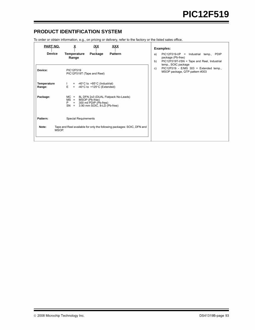
© 2008 Microchip Technology Inc. DS41319B-page 93
PIC12F519
PRODUCT IDENTIFICATION SYSTEMTo order or obtain information, e.g., on pricing or delivery, refer to the factory or the listed sales office.
PART NO. X /XX XXX
PatternPackageTemperatureRange
Device
Device: PIC12F519
PIC12F519T (Tape and Reel)
Temperature Range:
I = -40°C to +85°C (Industrial)E = -40°C to +125°C (Extended)
Package: MC = 8L DFN 2x3 (DUAL Flatpack No-Leads)MS = MSOP (Pb-free)P = 300 mil PDIP (Pb-free)SN = 3.90 mm SOIC, 8-LD (Pb-free)
Pattern: Special Requirements
Examples:a) PIC12F519-I/P = Industrial temp., PDIP
package (Pb-free)b) PIC12F519T-I/SN = Tape and Reel, Industrial
temp., SOIC packagec) PIC12F519 - E/MS 303 = Extended temp.,
MSOP package, QTP pattern #303
Note: Tape and Reel available for only the following packages: SOIC, DFN andMSOP.

DS41319B-page 94 © 2008 Microchip Technology Inc.
AMERICASCorporate Office2355 West Chandler Blvd.Chandler, AZ 85224-6199Tel: 480-792-7200 Fax: 480-792-7277Technical Support: http://support.microchip.comWeb Address: www.microchip.comAtlantaDuluth, GA Tel: 678-957-9614 Fax: 678-957-1455BostonWestborough, MA Tel: 774-760-0087 Fax: 774-760-0088ChicagoItasca, IL Tel: 630-285-0071 Fax: 630-285-0075DallasAddison, TX Tel: 972-818-7423 Fax: 972-818-2924DetroitFarmington Hills, MI Tel: 248-538-2250Fax: 248-538-2260KokomoKokomo, IN Tel: 765-864-8360Fax: 765-864-8387Los AngelesMission Viejo, CA Tel: 949-462-9523 Fax: 949-462-9608Santa ClaraSanta Clara, CA Tel: 408-961-6444Fax: 408-961-6445TorontoMississauga, Ontario, CanadaTel: 905-673-0699 Fax: 905-673-6509
ASIA/PACIFICAsia Pacific OfficeSuites 3707-14, 37th FloorTower 6, The GatewayHarbour City, KowloonHong KongTel: 852-2401-1200Fax: 852-2401-3431Australia - SydneyTel: 61-2-9868-6733Fax: 61-2-9868-6755China - BeijingTel: 86-10-8528-2100 Fax: 86-10-8528-2104China - ChengduTel: 86-28-8665-5511Fax: 86-28-8665-7889China - Hong Kong SARTel: 852-2401-1200 Fax: 852-2401-3431China - NanjingTel: 86-25-8473-2460Fax: 86-25-8473-2470China - QingdaoTel: 86-532-8502-7355Fax: 86-532-8502-7205China - ShanghaiTel: 86-21-5407-5533 Fax: 86-21-5407-5066China - ShenyangTel: 86-24-2334-2829Fax: 86-24-2334-2393China - ShenzhenTel: 86-755-8203-2660 Fax: 86-755-8203-1760China - WuhanTel: 86-27-5980-5300Fax: 86-27-5980-5118China - XiamenTel: 86-592-2388138 Fax: 86-592-2388130China - XianTel: 86-29-8833-7252Fax: 86-29-8833-7256China - ZhuhaiTel: 86-756-3210040 Fax: 86-756-3210049
ASIA/PACIFICIndia - BangaloreTel: 91-80-4182-8400 Fax: 91-80-4182-8422India - New DelhiTel: 91-11-4160-8631Fax: 91-11-4160-8632India - PuneTel: 91-20-2566-1512Fax: 91-20-2566-1513Japan - YokohamaTel: 81-45-471- 6166 Fax: 81-45-471-6122Korea - DaeguTel: 82-53-744-4301Fax: 82-53-744-4302Korea - SeoulTel: 82-2-554-7200Fax: 82-2-558-5932 or 82-2-558-5934Malaysia - Kuala LumpurTel: 60-3-6201-9857Fax: 60-3-6201-9859Malaysia - PenangTel: 60-4-227-8870Fax: 60-4-227-4068Philippines - ManilaTel: 63-2-634-9065Fax: 63-2-634-9069SingaporeTel: 65-6334-8870Fax: 65-6334-8850Taiwan - Hsin ChuTel: 886-3-572-9526Fax: 886-3-572-6459Taiwan - KaohsiungTel: 886-7-536-4818Fax: 886-7-536-4803Taiwan - TaipeiTel: 886-2-2500-6610 Fax: 886-2-2508-0102Thailand - BangkokTel: 66-2-694-1351Fax: 66-2-694-1350
EUROPEAustria - WelsTel: 43-7242-2244-39Fax: 43-7242-2244-393Denmark - CopenhagenTel: 45-4450-2828 Fax: 45-4485-2829France - ParisTel: 33-1-69-53-63-20 Fax: 33-1-69-30-90-79Germany - MunichTel: 49-89-627-144-0 Fax: 49-89-627-144-44Italy - Milan Tel: 39-0331-742611 Fax: 39-0331-466781Netherlands - DrunenTel: 31-416-690399 Fax: 31-416-690340Spain - MadridTel: 34-91-708-08-90Fax: 34-91-708-08-91UK - WokinghamTel: 44-118-921-5869Fax: 44-118-921-5820
WORLDWIDE SALES AND SERVICE
01/02/08