GaN-Based Tri-Gate High Electron Mobility Transistors
171
Albert-Ludwigs University of Freiburg Faculty of Engineering – GaN-Based Tri-Gate High Electron Mobility Transistors Dissertation submitted in partial fulfilment of the requirements for the degree of Doktor-Ingenieur by M. Sc. Erdin Ture December 2016
Transcript of GaN-Based Tri-Gate High Electron Mobility Transistors

Albert-Ludwigs University of FreiburgFaculty of Engineering –
GaN-Based Tri-Gate HighElectron Mobility Transistors
Dissertation
submitted in partial fulfilment of therequirements for the degree of
Doktor-Ingenieurby
M. Sc. Erdin Ture
December 2016

ii
Dekan
Prof. Dr. sc. nat. Oliver Paul
Referenten
Prof. Dr. rer. nat. Oliver Ambacher
Prof. Dr. Colombo Bolognesi
Prof. Dr. Tomas Palacios
Datum der Disputation
03.08.2017

Abstract
The rapidly-growing data throughput rates in a wide range of wirelesscommunication applications are pushing the established semiconductordevice technologies to their limits. Considerably higher levels of solid-state output power will therefore be needed to meet the demand in thenext generation satellite communications as well as the RADAR systems.Owing to their superior material properties such as high breakdown fieldsand peak electron velocities, GaN-based high electron mobility transistors(HEMTs) have recently prevailed in high-power systems operating in themicrowave frequency bands. On the other hand, technologies based onGaAs or InP still make up a large portion of the state-of-the-art devicesand circuits at the millimetre-wave (MMW) and sub-MMW frequencies.Due to the strong dependence of the intrinsic device parameters on theapplied bias point, highly-scaled GaN HEMTs are prone to experiencingdeteriorated high frequency characteristics which severely limit the high-power performance as well. Here, the relatively poor control of the gateelectrode is known to be the underlying root of the performance drop.In an attempt to overcome this by means of reinforcing the gate-control,3-dimensional GaN HEMT devices featuring the Tri-gate topology aredeveloped in this work, exhibiting enhanced performance in terms of bothoff- and on-state figures of merit.
One of the first obstacles is establishing a Tri-gate process scheme thatis fully compatible with the planar-gate GaN HEMT process, allowingfor a straightforward integration. On that account, electron-beam-definedmesa etching is found to be the most applicable method for patterning thenano-channels which constitute the Tri-gate FETs with promising devicecharacteristics. It is then shown that a thorough optimisation of the fingeometry and a 3-D passivation approach help improving the on-state DCperformance as well as suppressing the short channel effects (SCE) in theoff-state. By taking advantage of the superior gate-control, normally-off

iv
AlGaN/GaN FinFETs are subsequently presented with as high as +0.2 Vof threshold and 60 V of breakdown voltages, as opposed to -1.7 V ofthreshold and 28 V of breakdown voltages achieved by the conventionalGaN FETs. In order to further improve the on-state performance, advancedheterostructures with InAlGaN and AlN barriers are employed which resultin up to 3.8 A/mm of saturation drain current density, being one of thehighest recorded values among GaN-based Tri-gate devices. Followingthe DC-improvements, both small- and large-signal parameters of theTri-gate HEMTs are then optimised towards a more linear behaviour withrespect to the bias point. Once again, with the help of alternative barrierlayers and the reduction of the parasitic gate capacitances, a flatter RF-transconductance behaviour is achieved, leading to a bias-independentcurrent-gain cut-off frequency (𝑓T) of higher than 60 GHz. It is alsorevealed by the large-signal load-pull investigation that a maximum RFoutput power density of 3.7 W/mm (compared to 2.5 W/mm of theplanar FETs) can be reached by the AlN/GaN FinFETs while showing asimultaneous 𝑓T of 80 GHz. Finally, the presented W-band power amplifierwith 30 dBm of saturated output power and logic inverter designs for thefirst time demonstrate the excellent circuit-level performance of the GaN-based Tri-gate devices.
In the end, the developed GaN Tri-gate technology is proven to be a viablecandidate for achieving significantly higher RF output power withoutundergoing a cut-off frequency degradation. The demonstrated results ofthe fabricated monolithic microwave integrated circuits (MMICs) withWatt-level output power up to 90 GHz also promote the great potentialof Tri-gate FETs for both MMW power amplifier and high-speed logicapplications.

Zusammenfassung
Die schnell wachsenden Datenraten im Bereich der drahtlosen Kom-munikation bringen die etablierten Halbleitertechnologien an ihr Limit.Betrachtlich hohere Ausgangsleistungen werden von Halbleiterbauele-menten fur die nachste Generation der Satellitenkommunikations-systemeund Radarsysteme benotigt. Aufgrund ihrer uberlegenen Materialeigen-schaften (hohe Durchbruchspannung und Elektronen-geschwindigkeit) ha-ben sich GaN-basierte High Electron Mobility Transistors (HEMTs) imBereich der Mikrowellen-Hochleistungs-systeme durchgesetzt. Wegen dieserattraktiven Merkmale ist es gewunscht, GaN-Bauelemente fur Schaltkreiseim Bereich der Millimeterwellen- (MMW) und sub-MMW-Frequenzenzu etablieren. Auf der anderen Seite ist die Gate-Steuerwirkung derhochgradig skalierten GaN HEMTs auf den Kanal unzureichend. Diesverringert den wahlbaren Bereich des Arbeitspunktes fur einen Betriebs-zustand mit maximaler Großsignal-Aussteuerung. Dadurch werden dieLeistungsdichten nachhaltig beeintrachtigt. In dieser Arbeit werden dreidi-mensionale GaN HEMTs mit einer Tri-Gate-Topologie entwickelt, um dieseProbleme zu uberwinden. Damit wird die Gate-Kontrollierbarkeit erhohtund verbesserte Leistungsdaten sowohl im Sperr- als auch im leitendenZustand erreicht.
Eines der ersten Hindernisse ist es, ein Tri-Gate-Prozessschema zu er-stellen, das vollstandig mit dem Planar-Gate GaN-HEMT-Prozess kom-patibel ist und daher eine unkomplizierte Integration erlaubt. Zu diesemZweck wird ein elektronenstrahldefinierter Mesa-Atz-Prozess eingefuhrt,um Nanokanale zu strukturieren, die die Tri-Gate HEMTs bilden, mitdreidimensionaler Gate-Struktur. Es wird gezeigt, dass eine gezielte Op-timierung der Fin-Geometrie und ein 3D-Passivierungsansatz das DC-Verhalten im leitenden Zustand verbessern und daruber hinaus Kurzkanal-effekte im Sperrzustand unterdrucken. Aufgrund der verbesserten Gate-Kontrolle konnen im Folgenden selbstsperrende AlGaN/GaN FinFETs

vi
prasentiert werden, die eine positive Schwellenspannung (𝑉th) von bis zu+0,2 V und eine Durchbruchspannung (𝑉br) von bis zu 60 V vorweisen(im Vergleich zu 𝑉th = -1,7 V und 𝑉br = 28 V der Planar-FETs). Umdas Betriebsverhalten im leitenden Zustand weiter zu verbessern, wer-den fortgeschrittene Heterostrukturen mit InAlGaN- und AlN-Barrierengenutzt, welche einen Sattigungsstrom von bis zu 3,8 A/mm demonstrie-ren. Dieser Wert ist einer der hochsten aller veroffentlichten Tri-Gate-Bauelemente. Darauffolgend werden die Klein- als auch Großsignalpa-rameter des Tri-Gate-Bauelements in Richtung eines lineareren Verhal-tens bezuglich des Arbeitspunktes optimiert. Unter erneuter Verwen-dung alternativer Grenzschichten und der Reduktion der parasitarenGatekapazitat wird eine flachere RF-Transkonduktanz erreicht, die zueiner Arbeitspunkt-unabhangigen Grenzfrequenz der Stromverstarkung(Transitfrequenz) von uber 60 GHz fuhrt. Es wird ferner durch Großsignal-load-pull-Messungen gezeigt, dass die AlN/GaN FinFETs eine maximaleRF-Ausgangsleistungsdichte von 3,7 W/mm (im Vergleich zu 2,5 W/mmder Planar-FETs) bei gleichzeitiger Transitfrequenz von uber 80 GHz errei-chen konnen. Schließlich werden die exzellenten Leistungsdaten (30 dBmAusgangsleistung im W-band) der GaN-basierten Tri-Gate-Bauelementeauf Schaltungsebene durch aufgebaute MMW-Leistungsverstarker demons-triert.
Zusammenfassend beweist die entwickelte GaN Tri-Gate-Technologie, dasssie ein praktikabler Kandidat fur signifikant hohere RF-Ausgangsleistungenist, ohne dabei eine Degradation der Grenzfrequenz in Kauf nehmen zumussen. Die demonstrierten Resultate lassen das große Potenzial vonTri-Gate FETs sowohl fur MMW Leistungsverstarker als auch fur Logik-Anwendungen erkennen.

Contents
1. Introduction 11.1. Motivation for GaN Tri-gate . . . . . . . . . . . . . . . . . 11.2. State-of-the-art Technology . . . . . . . . . . . . . . . . . 4
1.2.1. GaN HEMTs for Millimetre-Wave Applications . . 51.2.2. Si and GaN Tri-gate Technology Comparison . . . 7
2. Fundamentals of GaN-Based HEMT Devices 92.1. Process Technology and Device Fabrication . . . . . . . . 9
2.1.1. Growth of AlGaN/GaN Heterostructures . . . . . 102.1.2. Alternative Barrier Structures for GaN HEMTs . . 122.1.3. Fabrication of GaN HEMTs . . . . . . . . . . . . . 15
2.2. Millimetre-Wave GaN HEMT Technology . . . . . . . . . 172.2.1. Conventional GaN HEMT DC Characteristics . . . 182.2.2. Small- and Large-Signal Figures of Merit . . . . . 21
2.3. Chapter Conclusion . . . . . . . . . . . . . . . . . . . . . 24
3. Analysis of the Short Channel Effects 253.1. Drain Induced Short Channel Effects . . . . . . . . . . . . 25
3.1.1. Sub-Threshold Characteristics and Leakages . . . 263.1.2. Bias Dependence of the Performance . . . . . . . . 29
3.2. Investigation of the Threshold Voltage . . . . . . . . . . . 323.2.1. Normally-Off Operation . . . . . . . . . . . . . . . 333.2.2. Integration of E/D Mode HEMTs . . . . . . . . . . 35
3.3. Chapter Conclusion . . . . . . . . . . . . . . . . . . . . . 36
4. Design of GaN Tri-gate HEMTs 374.1. 3-Dimensional Device Fabrication . . . . . . . . . . . . . . 374.2. Process Development . . . . . . . . . . . . . . . . . . . . . 43
4.2.1. 3-D Mesa Nano-Channel Patterning . . . . . . . . 434.2.2. Investigation of 3-D Surface Passivation . . . . . . 46
viii Contents
4.3. Design Aspects of the Tri-gate FETs . . . . . . . . . . . . 504.3.1. Device Geometry Considerations . . . . . . . . . . 514.3.2. Suppression of the Short Channel Effects . . . . . 604.3.3. Design of Normally-Off HEMTs . . . . . . . . . . . 62
4.4. Investigation of Heterostructure Variations . . . . . . . . . 694.4.1. Impact of the Barrier on Electrical Properties . . . 694.4.2. Development of High-Current Tri-gate HEMTs . . 75
4.5. Analysis of the Thermal Behaviour . . . . . . . . . . . . . 794.6. Chapter Conclusion . . . . . . . . . . . . . . . . . . . . . 82
5. Millimetre-Wave Performance of Tri-gate FETs 855.1. RF Characterisation of Tri-gate HEMTs . . . . . . . . . . 85
5.1.1. Reduction of the Gate Capacitance . . . . . . . . . 895.1.2. Improvement of the Intrinsic HF Parameters . . . 92
5.2. Small-Signal Tri-gate Performance . . . . . . . . . . . . . 955.2.1. Development of High-Gain Tri-gate HEMTs . . . . 955.2.2. Investigation on the RF Linearity of Tri-gate . . . 99
5.3. Large-Signal Tri-gate Performance . . . . . . . . . . . . . 1045.4. Chapter Conclusion . . . . . . . . . . . . . . . . . . . . . 110
6. GaN Tri-gate Demonstrator Circuits 1136.1. Millimetre-Wave Power Amplifiers . . . . . . . . . . . . . 113
6.1.1. Pre-Matched High-Power Tri-gate FETs . . . . . . 1146.1.2. GaN Tri-gate MMW Power Amplifier MMIC . . . 117
6.2. Integrated Mixed-Signal Circuits . . . . . . . . . . . . . . 1216.2.1. High-Speed Direct Coupled FET Logics . . . . . . 1216.2.2. Integrated E/D Mode Cascode Inverter . . . . . . 122
6.3. Chapter Conclusion . . . . . . . . . . . . . . . . . . . . . 124
7. Conclusion and Outlook 1257.1. Summary and Conclusion . . . . . . . . . . . . . . . . . . 1257.2. Outlook . . . . . . . . . . . . . . . . . . . . . . . . . . . . 128
References 129

List of Abbreviations
2DEG Two-dimensional electron gasAlGaN Aluminium gallium nitrideAlN Aluminium nitrideCAD Computer aided designCMOS Complementary metal oxide semiconductorCPW Coplanar waveguideCS Common-sourceCW Continuous waveDC Direct currentDE Drain efficiencyDIBL Drain induced barrier loweringFET Field effect transistorFIB Focused ion beamGaAs Gallium arsenideGaN Gallium nitrideGCPW Grounded coplanar waveguideHBT Heterojunction bipolar transistorHEMT High electron mobility transistorHF High frequencyHFSS High Frequency Structural Simulator by Ansys Inc.ICP Inductively coupled plasmaIMN Input matching networkInAlGaN Indium aluminium gallium nitrideInP Indium phosphideISMN Inter-stage matching networkLP Load-pull

x List of Abbreviations
MAG Maximum available gainMBE Molecular beam epitaxyMIM Metal-insulator-metalMISFET Metal insulator semiconductor field effect transistorMMIC Monolithic microwave integrated circuitMMW Millimetre-waveMOCVD Metal-organic chemical vapour depositionMOSFET Metal oxide semiconductor field effect transistorMSG Maximum stable gainMSL Microstrip lineNi NickelNiCr Nickel-chromiumOMN Output matching networkPA Power amplifierPAE Power added efficiencyPECVD Plasma-enhanced chemical vapour depositionpHEMT Pseudomorphic high electron mobility transistorPt PlatinumRADAR Radio detection and rangingRF Radio frequencyRIE Reactive ion etchingSCE Short channel effectsSEM Scanning-electron-microscopeSi SiliconSiC Silicon carbideSiGe Silicon germaniumSiN Silicon nitrideSS Sub-threshold swingSSPA Solid state power amplifierTGW Total gate-widthTi TitaniumTMAH Tetramethyl ammonium hydroxide

List of Symbols
𝐶ds Intrinsic drain-source capacitance𝐶gd Intrinsic gate-drain capacitance𝐶gs Intrinsic gate-source capacitance𝑑bar Barrier thickness𝑑SiN Silicon nitride passivation layer thickness𝐸br Breakdown field𝐸C Conduction band energy𝐸F Fermi energy𝐸g Band gap energy𝐸V Valance band energy𝜀0 Vacuum permittivity𝜀r Relative permittivity (dielectric constant)𝑓max Maximum frequency of oscillation𝑓T Current-gain cut-off frequency𝑔ds Intrinsic output conductance𝑔m Intrinsic transconductance𝐺P Large-signal power gainℎ21 Current-gainℎ Planck constant𝐼G Extrinsic gate current𝐼D,min Minimum drain leakage current𝐼D,sat Maximum saturated drain current𝑘 Boltzmann constant𝜅 Thermal conductivity𝐿fin Length of fin-shaped nano-channels𝐿g Gate length

xii List of Symbols
𝐿gd Gate-drain spacing𝐿gs Gate-source spacing𝑚* Effective mass of electrons𝜇0 Electron mobility𝑛s Sheet carrier concentration𝑃DC Dissipated DC-power𝑃in RF input power𝑃out RF output power𝑝pi Piezo-electric polarization𝑝sp Spontaneous polarizationΦB Schottky barrier height𝑞 Elementary charge𝑅cont Contact resistance𝑅d Drain resistance𝑅g Gate resistance𝑅on On-resistance𝑅s Source resistance𝑅sheet Sheet resistance𝑅th Thermal resistance𝑆11 Input reflection coefficient𝑆12 Reverse transmission coefficient𝑆21 Forward transmission coefficient𝑆22 Output reflection coefficient𝜎 Polarization sheet charge𝑉br Breakdown voltage𝑉DS Drain-source voltage𝑣e Electron velocity𝑉GS Gate-source voltage𝑉k Knee voltage𝑉th Threshold voltage𝑊fin Width of fin-shaped nano-channels𝑊trench Width of trenches

1. Introduction
1.1. Motivation for GaN Tri-gate
The ever-increasing demand for semiconductor technologies towards therealisation of high-speed systems and networks with multi-gigabit datatraffic rates have prompted for the assessment of new material systems aswell as novel device topologies over the years. Particularly in satellite or,in general, point-to-point communications, recent wireless communicationstandards are being released in the millimetre-wave (MMW) frequenciesin order to enable higher data rates. As much as the device speed occursto be an important performance criterion, the maximum radio frequency(RF) output power a device can deliver is another critical parameter formost of the MMW applications. To be able to overcome the free-spacepath loss in long-range wireless backhaul links, the transmitter componentswithin the corresponding systems are required to emit sufficient levels ofsignal power. In addition to wireless communications, the need for higherRF output power can also be acknowledged in radio detection and ranging(RADAR) applications as well as the sensor systems for remote sensing.
Typically, gallium arsenide (GaAs)- and silicon (Si)-based field effecttransistors (FET) or indium phosphide (InP)-based heterojunction bipolartransistors (HBT) are dominantly-used in amplifiers for very high frequency(MMW or sub-MMW) applications with medium levels of output power.However, their limited maximum operation voltages prevent from meetingthe desired output power requirements in the mentioned applications. Onthe other hand, vacuum tube amplifiers are still being employed for veryhigh power applications due to their unprecedented RF output powerlevels. Therefore the cost, weight, and maintenance constraints, to whichtube amplifiers cannot comply, evoke the need for high-power solid-stateamplifiers in the MMW applications.

2 Introduction
The investigation of wide band gap materials with remarkable propertiessuch as gallium nitride (GaN) has revealed substantial benefits for poweramplifier (PA) applications over the existing Si-based technologies. Bytaking advantage of the high-voltage operation as well as the improvedchannel transport mechanism, AlGaN/GaN high electron mobility transis-tors (HEMT) have already been demonstrated to be superior candidatesover Si with high RF-power performance and exceptional breakdown volt-ages in power electronics [1] while, up to 30 W/mm of unrivalled microwaveoutput power densities have been reported up to 10 GHz [2,3].
In spite of the advantages that GaN HEMTs possess at microwave fre-quencies, downscaling of the device geometry towards achieving higherspeeds introduces significant challenges to be overcome that are relatedto the short channel effects (SCE) which ultimately impair the powerperformance. Even though considerable work has recently been investedinto highly-scaled devices, not many established GaN technologies arein existence, capable of delivering adequate RF power at the MMW fre-quencies. Thus, the MMW performance of GaN-based devices has to beimproved in terms of output power, to be able to compete with the tubeamplifiers.
It has already been determined in Si-based CMOS technology that a3-dimensional channel and gate profile (denoted as Tri-gate) greatly miti-gates the SCE. In that regard, the Tri-gate device topology emerges as afeasible candidate, whose potential in MMW power amplifier applicationshave never been looked into prior to this work. Accordingly, a systematicinvestigation that is undertaken in this research will unveil the promisingpotential of the infant GaN Tri-gate technology.
Based on the achievements and experiences in the CMOS industry theadoption of the Tri-gate approach in GaN HEMT technology is expected toaccommodate following enhancements. Degradation of the RF performancewith respect to the bias point is one of the most critical issues which needsto be improved through GaN Tri-gate device development. The ability ofthe Tri-gate electrode to gain higher control over the channel will lead tomore linear transconductance and cut-off frequency responses, reducingthe bias dependence. Consequently, a more robust transistor operation ata higher dynamic voltage swing can be established without experiencingdrops in the frequency performance. The saturation current density is also

1.1. Motivation for GaN Tri-gate 3
expected to be boosted as a result of a higher effective electron velocitysupported by the uniform electric field distribution within the Tri-gatechannel. In combination with the higher operation drain bias voltages tobe achieved by Tri-gate GaN HEMTs, the increased drain current levelswill help in reaching an up to two-fold raise in the RF output power densityat MMW frequencies. Furthermore, providing the normally-off operationis considered to be another crucial benefit for various applications suchas power electronics and high-speed logics. On the other hand, it can beforeseen that the Tri-gate devices are prone to exhibiting slight increasesin the gate capacitance and declines in the maximum achievable cut-offfrequencies. Nevertheless, the above-mentioned advantages of the Tri-gatetopology are predicted to outweigh the potential drawbacks which are allsummarised in Table 1.1.
Table 1.1.: Predicted properties of the GaN-based Tri-gate devices compared to theconventional GaN HEMTs for the gate length: 𝐿g = 100 nm.
Device Technology/Estimated Parameter Conventional GaN HEMT Tri-gate GaN HEMT
Max. drain current <1.5 A/mm >2 A/mm
Max. operation 𝑉DS <15 V >20 V
𝑔m and 𝑓T linearitynon-linear and
strongly bias-dependentlinear and
bias-independent
MMW power density ˜2 W/mm ˜4 W/mm
Gate capacitance ˜0.5 pF/mm ˜0.6 pF/mm
Peak 𝑓T ˜100 GHz ≤100 GHz
RF parasitics FET layout-definedunaffected
(layout-defined)
Device operationnormally-on
(D-mode HEMT)normally-off
(E- and D-mode)

4 Introduction
Regarding the outline of the thesis, the fundamentals and recent ad-vances in GaN-based technologies will be summarised, followed by a briefcomparison of the proposed GaN Tri-gate approach to the CMOS counter-part throughout this Chapter. In Chapter 2, theoretical analysis of theconventional GaN HEMTs will be reviewed with a focus on the processtechnology and suitability to MMW operation. Chapter 3 will then detailthe challenges which are faced in short-channel GaN devices as the scalingproperties will be elucidated. The design and development procedure ofGaN Tri-gate HEMTs will be given in Chapter 4, leading to enhanceddevice characteristics. Chapter 5 will subsequently demonstrate the MMWpower performance of the designed Tri-gate FETs. Finally in Chapter 6,circuit-level performance of the developed technology will be presented.
1.2. State-of-the-art Technology
Falling into the category of wide band gap materials, GaN features appeal-ing attributes in comparison to the competing state-of-the-art materialtechnologies such as Si or GaAs. Table 1.2. summarises the key param-eters of dominant semiconductor technologies for microwave and MMWapplications. Owing to its large band gap, GaN inherits tremendous break-down fields, up to 10 times higher than Si, which is often regarded as themain advantage of GaN devices. This crucial asset is powerful enough toovercome its shortcomings (i.e. low-field mobility) and the potential ofthis material system has been recognised in a variety of applications.
The advantageous properties of GaN have first of all emerged in the fieldof power electronics. By adopting either metal oxide or metal insulatorsemiconductor field effect transistor (MOSFET, MISFET) architecturesand engineered field plate designs to optimise the breakdown voltages,reliable and highly-efficient operation at and over 600 V has been demon-strated [4–7]. Combined with the adequate electron velocities, the achievedhigh saturation current densities in excess of 2 A/mm have also promotedthe suitability of GaN HEMTs for PAs based on monolithic microwaveintegrated circuits (MMIC) [8, 9]. Hence, the most recent reviews andstudies support that GaN has successfully taken the lead in a wide rangeof application fields [9, 10].

1.2. State-of-the-art Technology 5
Table 1.2.: Properties of common semiconductor materials used in RF applications [1].
Material/Parameter Si SiC GaAs InP GaN
Band gap(𝐸g) [eV] 1.1 3.26 1.42 1.34 3.4
Breakdown field(𝐸br) [106 V/cm] 0.3 3.0 0.4 0.5 3.3
Electron mobility(𝜇0) [cm2/Vs] 1350 700 8500 10000 1600
Saturation electronvelocity (𝑣e) [107 cm/s] 1.0 2.0 1.3 1.0 2.5
Thermal conductivity(𝜅) [W/cmK] 1.5 4.9 0.46 0.68 1.3
1.2.1. GaN HEMTs for Millimetre-Wave Applications
In addition to the dominance of GaN HEMTs in the microwave regime,recent advances in device development have also enabled the realisationof amplifiers and various MMICs operating in the MMW frequencies.Notably, in the area of power amplifier design, on-chip power levels inexcess of 3 W in the frequency range 80 – 100 GHz have been reported,exhibiting high efficiencies up to 20% [11,12]. A comparison of state-of-the-art semiconductor technologies [13–29] in terms of respective current-gaincut-off frequencies (𝑓T) and maximum RF output power densities (𝑃out) ispresented in Fig. 1.1. There, it is evident that the MMW power densitiesdelivered by the competing material systems such as GaAs, InP, or silicongermanium (SiGe) are unable to match to those of GaN-based devices. Onthe lower end of millimetre-wave spectrum, at around 30–40 GHz, almost10 W/mm of 𝑃out has been proven while dropping below 1.7 W/mm at200 GHz which fits to the commonly-acknowledged 1/𝑓2 relationship ofthe output power with respect to frequency.

6 Introduction
Figure 1.1.: Overview of the state-of-the-art device technologies for MMW poweramplifier applications compared in regard to cut-off frequency (𝑓T) and output powerdensity (𝑃out).
Besides the development of MMW GaN technologies, exploiting the highfrequency (HF) potential in the sub-MMW range appears as anotherrecent field of research. Even though InP and GaAs-based devices stillexcel in applications with operation frequencies of higher than 200 GHz,innovative technologies in GaN devices towards scaling the gate length intothe deep sub-micron region have extended the usable frequency range intothe sub-MMW regime. Initially, the adoption of advanced heterostructureswith a nearly lattice-matched InAlN barrier has improved the cut-offfrequencies up to 205 GHz [30]. The optimisation of the T-gate structurewith minimised parasitic fields has then reduced the gate capacitanceas well as the gate resistance, subsequently allowing for the operationabove 300 GHz [31, 32]. Most recently, the development of regrown ohmiccontacts [33] and self-aligned 20-nm-long gate processes [34–36] have ledto boosted 𝑓T figures as high as 450 GHz [37,38].

1.2. State-of-the-art Technology 7
1.2.2. Si and GaN Tri-gate Technology Comparison
Since the scope of this work involves establishing the design and fabricationof high-performance Tri-gate devices, the origins of the technology needsto be reviewed. Even though the first examples of Tri-gate FinFETs havebeen introduced by the Si-based complementary metal oxide semiconductor(CMOS) industry [39,40], both the motive and implementation of Tri-gatetechnology in GaN differ from CMOS in principle aspects, albeit showingsimilarities regarding the short-channel device scaling.
Overcoming the efficiency reduction in aggressively-scaled CMOS devicesby managing the off-state leakage currents has been the main motive forSi-based Tri-gate. Extensive studies in the field of high-speed CMOS logicshave asserted that Tri-gate topology is a viable approach for suppressingthe SCE and attaining almost ideal sub-threshold characteristics closeto the theoretical limits [39]. Consequently, high-performance FinFETshave been demonstrated with successful a gate length scaling beyond20 nm [40]. Contrarily, reaching a high-power operation without sacrificingfrom the high frequency performance lies at the core of GaN-based Tri-gatemotivation.
Figure 1.2.: Timeline depicting the evolution of Si-based CMOS and GaN technologies[2, 13,22,42,43].

8 Introduction
In that sense, one of the fundamental problems of GaN HEMTs hasbeen put forward by Palacios et al. which is the negative influence oftheir strong bias dependence on the HF parameters [41]. It has beenshown that the dynamic resistance in the access region, in relation toan increase in the drain current, results in non-linear transconductanceand cut-off frequency behaviour over the bias point. In return, the powerperformance of a HF GaN device becomes strictly limited. Since theTri-gate topology greatly reduces the SCE, the detrimental effects dueto bias variation are expected to be minimised, with the intention ofrestoring the RF output power at MMW frequencies. Fig. 1.2. sets displayto the technological evolution and milestones achieved in Si-CMOS- andGaN-based semiconductor technologies.
Thereupon the main goal of this research is to develop highly-scaled MMWHEMTs with improved performance towards the use in high power amplifierapplications by means of combining the already-established GaN HEMTtechnology of Fraunhofer IAF and the Tri-gate architecture approach whichoriginates from the Si CMOS technology.

2. Fundamentals of GaN-BasedHEMT Devices
The development of novel transistor structures such as the GaN Tri-gatedevices requires a complete knowledge of the principles of relatively well-studied conventional high electron mobility transistors (HEMTs). Thisincludes understanding the basic material properties, analysing the devicephysics that is responsible for the transistor operation and characteristics,as well as reviewing the state-of-the-art performance in the literature.On that account the essential process steps regarding the growth of theepitaxial layers, fabrication scheme of the devices, and the most criticalmillimetre-wave (MMW) performance figures of merit of the sub-micronscaled GaN HEMTs will be presented in this Chapter.
2.1. Process Technology and Device Fabrication
In order to fabricate high-performance GaN devices a stable and well-established process technology is indispensable for any field effect transistor(FET) topology. The precision and accuracy that the technology offersin resolving the structures gains more importance in this work sinceparticularly small critical feature geometries are needed to form the nano-channels in the Tri-gate approach. Therefore, as a starting point, all ofthe modified process schemes for Tri-gate devices have been based on theexisting process technology with a corresponding gate length of 100 nm(denoted as GaN10) of Fraunhofer Institute for Applied Solid-State Physics(IAF) which allows the fabrication of both discrete HEMTs and completecircuits for MMW applications as some of its details will be discussed inthis Section.

10 Fundamentals of GaN-Based HEMT Devices
2.1.1. Growth of AlGaN/GaN Heterostructures
Prior to the introduction of the heterostructure growth, the principles ofa GaN HEMT device and its physics have to be revisited. Essentially, aGaN-based high electron mobility transistor structure comprises a GaNbuffer layer which is grown in the Ga-face orientation on top of a substratematerial (typically SiC), an AlGaN barrier layer, and a relatively thin GaNcap. The HEMT operation in this case takes advantage of the superiortransport properties of electrons with a very high sheet charge concen-tration (typically around 1013 cm−2) which also yield significantly highmobilities (as high as 2000 cm2/Vs at room temperature) provided by theinherent piezoelectric and spontaneous polarisation of the heterojunction.The piezoelectric polarisation part results from the crystal deformationcaused by the biaxial strain in the AlGaN layer since GaN and AlGaNhave different lattice constants. Asymmetry of the crystal and the dif-ference in the electro-negativities of nitrogen and metal atoms are thenresponsible for the spontaneous polarisation. Furthermore, a discontinuityof the conduction band (𝐸C) occurs between the two layers due to thedifferent band gap energies (𝐸g) of GaN and AlGaN. The correspondingband diagrams along the z-axis of the heterostructure are exhibited inFig. 2.1.
Figure 2.1.: Simulated diagram of the conduction band edge, valence band edge, andthe electron concentration in a conventional AlGaN/GaN HEMT structure with 11 nmof barrier and 2 nm of cap thickness.

2.1. Process Technology and Device Fabrication 11
In combination with this conduction band offset, total polarisation chargegradient between the AlGaN and GaN constructs a quantum potential wellwith a triangular shape, forming a so-called two-dimensional electron gas(2DEG) at the GaN/AlGaN interface [43]. Accordingly, the advantageousfeatures of GaN HEMTs originate from the conductive 2DEG channellayer, in which free electrons can benefit from an improved Hall mobilityas no interface roughness or intentional doping is present. The fact thatthe electron movement is confined within a quasi two-dimensional pathaway from the dopants in the barrier, reduces any interactions with theenvironment which helps electrons to be much less affected by phononscattering and recombination [44,45].
Concerning the growth of epitaxial heterostructures, either metal-organicchemical vapour deposition (MOCVD) or molecular beam epitaxy (MBE)reactors can be used to fabricate the AlGaN/GaN HEMTs based on the IAFGaN10 technology. A high yield of specimens with lower defect densitiescan be obtained through MOCVD growth whereas the MBE approachoffers more controlled growing conditions leading to more homogeneouslayers with very low surface roughness. Provided by its excellent thermalconductivity, similar lattice constant to GaN, and relatively low dielectricloss the semi-insulating (s.i.) SiC is used as the substrate material whichfeatures either 3 inches or 4 inches of diameter. First of all an AlNnucleation layer with a thickness of 100 – 120 nm is grown after cleaningthe SiC substrate. The nucleation layer holds a critical function for ensuringthe Ga-face polarity of the following layers. A 1.8-µm-thick isolating GaN-buffer layer is then grown on top of the AlN spacer which is needed toprevent the spreading of dislocations and stacking faults due to the latticemismatch. This is followed by the growth of an AlGaN barrier with highAl-contents up to 35%. The thickness of the barrier is considered to beone of the most critical parameters concerning the gate length (𝐿g) scaling.It has been demonstrated by Haupt et al. that a gate length to barrierthickness ratio of at least 10:1 has to be maintained to achieve a sufficientsuppression of the short channel effects [46]. In that regard, 11 nm ofthickness has already been established for the IAF GaN10 technology with𝐿g = 100 nm. Finally, the epitaxial growth is concluded with a GaN caplayer of 2-3 nm thickness. A long-term reliability of the device throughenhanced surface stability can be provided by the thin cap layer.

12 Fundamentals of GaN-Based HEMT Devices
Figure 2.2.: Cross-sectional schematic illustration of the processed AlGaN/GaN HEMTstructure grown on SiC substrate.
The adopted process technology for the growth of AlGaN/GaN heterostruc-tures focuses on obtaining high-quality wafers with improved electricalproperties such as reduced sheet and access resistances. By adjusting theAl-content in the barrier, as high as 1600 cm2/Vs of electron mobility andmore than 1013 cm−2 of sheet carrier density can be achieved, leading toaround 400 Ω/sq of sheet resistance. Thereupon, the fabrication of high-performance GaN HEMTs with maximum transconductance is expedited.Fig. 2.2. illustrates the layer sequence of the fully-processed AlGaN/GaNHEMTs in the active area.
2.1.2. Alternative Barrier Structures for GaN HEMTs
As mentioned earlier, the 2DEG channel in the AlGaN/GaN HEMT isinduced by the polarisation effects. The sum of piezoelectric polarisation(𝑝pi) of the strained AlGaN barrier and the spontaneous polarisation (𝑝sp)within unstrained GaN and AlGaN crystals generates a strong electricfield that is proportional to the total sheet charge (𝜎) as described by theequation [47]:
𝜎
𝑞= Δ𝑝 = (𝑝pi,AlGaN + 𝑝sp,AlGaN) − 𝑝sp,GaN, (2.1)

2.1. Process Technology and Device Fabrication 13
which results in the following sheet carrier density:
𝑛s = 𝜎
𝑞− 𝜀0𝜀r
𝑞2𝑑bar· (𝜓 + 𝐸F − Δ𝐸C + 𝑉GS), (2.2)
where 𝑞 denotes the elementary charge, 𝜀r is the relative permittivity ofAlGaN, 𝑑bar is the thickness of the barrier, 𝜓 is the surface potential, 𝐸F isthe Fermi level, and 𝑉GS is the applied external voltage at the gate. Thissignifies that the channel properties can be altered through the adjustmentof the barrier thickness and composition. Once the fraction of Al in thebarrier is increased, the sheet carrier concentration can be boosted whilelowering the sheet resistance. On the other hand, dramatic reductionsin the low-field carrier mobility can be observed at Al-contents of higherthan 32% as a result of the emerging alloy scattering [48]. Hence, 32%of Al-concentration is considered to be the optimum value for the bestHEMT performance in terms of gain and output power.
A similar trade-off point must be found in the thickness of the barrier aswell. Fundamentally, the sheet carrier density exhibits an increasing trendas the AlGaN barrier becomes thicker up to a certain point where thedensity of electrons can no longer be raised and a saturation is reached.In addition to this, the relaxation of the layer which compensates thetensile strain limits the practical maximum barrier height since high defectdensities and cracking begin to occur above a critical thickness. On theother hand, less distance between the channel and the gate electrode isrequired in devices with highly-scaled 𝐿g to gain more control over the2DEG and minimise the adverse effects of the short channel. However,growing a very thin barrier bears the potential threat of elevated gateleakage currents and high frequency dispersion. Therefore, assessing a𝑑bar that is a factor of 10 smaller than the 𝐿g shows the best compromisebetween electrical properties and parasitic effects.
Concerning the influence of the parasitics, the source resistance is a criticalparasitic element which can be detrimental for the extrinsic transconduc-tance. The gate-voltage drop caused by the source resistance reduces theextrinsic transconductance and deteriorates the performance of HEMTdevices. The total source resistance can be described as follows:

14 Fundamentals of GaN-Based HEMT Devices
𝑅s = 𝑅sheet +𝑅cont, (2.3)
where 𝑅sheet and 𝑅cont are sheet and contact resistances, respectively. Thesheet resistance here is directly related to the gate-source spacing (𝐿gs)and is given as:
𝑅sheet = 𝐿gs
𝑞 · 𝜇0𝑛s(2.4)
In relation to the intrinsic value, the extrinsic transconductance can thenbe given as:
𝑔m,ext = 𝑔m,int
1 +𝑅s𝑔m,int(2.5)
It can be interpreted that the source resistance needs to be decreased inorder to obtain high extrinsic transconductance, for which the epitaxialparameters such as the mobility and sheet carrier density have to bemaximised.
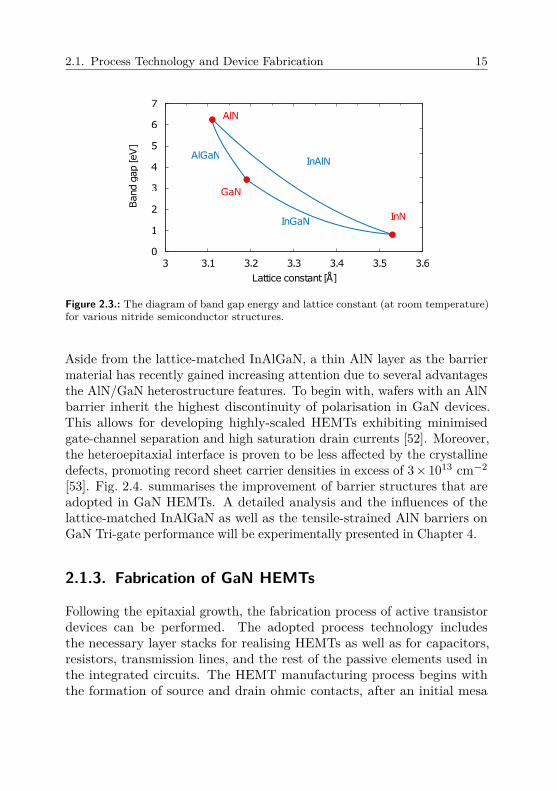
Taking the above-mentioned limitations of the conventional AlGaN bar-rier into account, alternative material structures can be considered asprospective barriers for advanced GaN HEMTs with improved perfor-mance. Revealing those alternatives, the band gap energies over the latticeconstant of AlN, GaN, and InN are illustrated in Fig. 2.3. where theternary alloys can also be depicted. One of the viable options is thelattice-matched quaternary InAlGaN material. By replacing the AlGaNbarrier with InAlGaN, the spontaneous polarisation is expected to becomestronger through the incorporation of Al. Another benefit of a quaternarybarrier is the larger degree of freedom in controlling band gap and latticeconstant independently. Consequently, a denser 2DEG can be achievedby using a lattice-matched interface [49,50]. Compared to an alternativeternary InAlN structure which significantly suffers from interface roughnessscattering, the InAlGaN variant possesses a further advantage of reducingthe miscibility gaps, allowing the highest mobility values to be reached(1900 cm2/Vs) among lattice-matched GaN heterostructures [51].
2.1. Process Technology and Device Fabrication 15
Figure 2.3.: The diagram of band gap energy and lattice constant (at room temperature)for various nitride semiconductor structures.
Aside from the lattice-matched InAlGaN, a thin AlN layer as the barriermaterial has recently gained increasing attention due to several advantagesthe AlN/GaN heterostructure features. To begin with, wafers with an AlNbarrier inherit the highest discontinuity of polarisation in GaN devices.This allows for developing highly-scaled HEMTs exhibiting minimisedgate-channel separation and high saturation drain currents [52]. Moreover,the heteroepitaxial interface is proven to be less affected by the crystallinedefects, promoting record sheet carrier densities in excess of 3 × 1013 cm−2
[53]. Fig. 2.4. summarises the improvement of barrier structures that areadopted in GaN HEMTs. A detailed analysis and the influences of thelattice-matched InAlGaN as well as the tensile-strained AlN barriers onGaN Tri-gate performance will be experimentally presented in Chapter 4.
2.1.3. Fabrication of GaN HEMTs
Following the epitaxial growth, the fabrication process of active transistordevices can be performed. The adopted process technology includesthe necessary layer stacks for realising HEMTs as well as for capacitors,resistors, transmission lines, and the rest of the passive elements used inthe integrated circuits. The HEMT manufacturing process begins withthe formation of source and drain ohmic contacts, after an initial mesa

16 Fundamentals of GaN-Based HEMT Devices
Figure 2.4.: Summary of the common epitaxial barrier layers and their respectivebeneficial properties in GaN HEMTs.
etching outside the active area. Optical stepper lithography is used todefine the contact pad areas since it is sufficient in resolving feature sizeslarger than 500 nm. Although, in case of defining relatively thicker lift-offresist layers, the critical dimension rises up to 1 µm. The evaporation ofan alloyed Ti/Al-based metal stack is then carried out which provides verylow (0.2 Ωmm) contact resistances to effectively minimise the parasiticcomponent of the on-resistance of the channel. In order to establish a high-quality ohmic contact between the 2DEG, the metal stack is made to diffuseinto the barrier through rapid thermal annealing at high temperaturesbetween 800 – 850 ∘C. Here, the homogeneity of the metal surface alsoplays a critical role in marking the reference for the subsequent masks.
The next critical step is the passivation of the surface in the active area.This procedure holds particular importance for GaN since its 2DEGproperties are prone to get affected by the charged surface states [54]. Astable HEMT operation with reduced low-frequency dispersion would onlybe possible when the channel is adequately protected from high electric fieldpeaks. Plasma-enhanced chemical vapour deposition (PECVD) is thereforeused to deposit the first Si3N4 passivation layer. As for the defining ofthe gate opening, electron beam (e-beam) lithography is utilised which iscapable of resolving the gate length of 100 nm. After the selective plasmaetching of the nitride layer, surface of the GaN material is exposed at thegate area where the Ni/Pt/Au-based T-gate module is deposited that forms

2.2. Millimetre-Wave GaN HEMT Technology 17
a Schottky contact. The unique T-shape of the gate electrode is the resultof a peculiar optimisation progress, serving as a compromise between lowgate-line resistance and parasitic capacitances. To complete the fabrication,PECVD is once again employed to deposit a final passivation layer toprotect the active area.
Figure 2.5.: Scanning-electron-microscope (SEM) perspective view of an IAF-processedAlGaN/GaN HEMT device with 4 gate fingers of 45 µm.
The passive process technology further accommodates metal-insulator-metal (MIM) capacitors capable of withstanding high voltages (> 50 V)and NiCr resistors for the monolithic microwave integrated circuit (MMIC)designs. A backside process then follows, once the SiC substrate is thinneddown to 75 µm. Finally, in order to provide contact to the backsidemetallisation, 30 × 30 µm2 through-wafer via holes are implemented. Ascanning-electron-microscope (SEM) image of a fully-processed conven-tional HEMT structure is exhibited in Fig. 2.5. As for comparison, Fig. 2.6.provides an overview of the 3-D structures to be formed after Tri-gateGaN HEMT fabrication which will be discussed in detail in Chapter 4.
2.2. Millimetre-Wave GaN HEMT Technology
It has been outlined that the realisation of high-speed FETs requiresthe successful accomplishment of a vertical epitaxial scaling as well asa lateral device scaling. Many challenges have been encountered and

18 Fundamentals of GaN-Based HEMT Devices
Figure 2.6.: Schematic 3-D illustration of the nano-channels and the gate-foot profile tobe achieved in the Tri-gate GaN HEMT design.
innovative solutions have been sought to be able to utilise GaN transistorsin the millimetre-wave (MMW) regime. The evaluation of the processtechnology for its use in MMW applications comes out as an integral partof the development progress. In that regard, determining the basic HEMTcharacteristics and the key performance parameters in both direct-current(DC) and radio frequency (RF) regime will be discussed in this Section forthe MMW operation.
2.2.1. Conventional GaN HEMT DC Characteristics
Through a complete DC-characterisation, the base performance of a HEMTdevice can be determined which serves as a first-order indicator of itssmall- and large-signal parameters. Being one of the basic performancemeasures of a transistor, the DC-transfer characteristics can be obtained bymeasuring the drain current (𝐼D) with respect to varied gate bias voltage(𝑉GS) at a fixed applied drain bias voltage (𝑉DS). Such DC-transferbehaviour of a GaN HEMT device as well as the relevant figures of meritcan be depicted Fig. 2.7. An immediate quantity that is attainable fromthe transfer characteristics is the threshold voltage (𝑉th) at which theonset of the drain current is observed and sets a border between the on-

2.2. Millimetre-Wave GaN HEMT Technology 19
Figure 2.7.: DC-transfer characteristics of a conventional GaN HEMT device measuredat 𝑉DS = 5 V, with its fundamental transistor parameters indicated.
and off-states of a FET. The extrinsic transconductance (𝑔m) is a morecritical figure of merit directly related to the high frequency maximumgain behaviour which is defined as the first derivative of the drain currentover 𝑉GS while keeping the 𝑉DS constant:
𝑔m = 𝜕𝐼D
𝜕𝑉GS
constant 𝑉DS
(2.6)
At this point, it is vital to note that most performance parameters ofboth discrete FETs and MMW amplifier circuits are considerably bias-dependent. Bias conditions are therefore highly-decisive on the resultingRF output power, efficiency, and linearity of an amplifier. As far asthe linear operation is concerned, a useful classification method is tocontemplate amplifier classes. The class-A operation is one of the mostbasic conditions in which the transistor is biased at a respective quiescentdrain current that is half of the saturation drain current 𝐼D,sat. In thiscase an ideal linear amplification can achieved without undergoing anyRF signal clipping, however, at the cost of decreased efficiency. In orderto regain the efficiency the transistor can be operated in class-B wherethe threshold voltage is selected as the DC bias point with zero quiescentcurrent. Similarly, an even lower bias point below the 𝑉th can be used to

20 Fundamentals of GaN-Based HEMT Devices
further increase the efficiency which leads to class-C operation. On theother hand, this results in dramatic reductions in the linearity, RF outputpower, and maximum attainable bandwidth. Finally, the class-AB biasserves as the compromise between class-A and B cases with reasonableefficiency and linearity. Such operation classes as well as the typical DC-transfer characteristics of a GaN HEMT are depicted in Fig. 2.7. It canbe noticed that the peak 𝑔m is observed at the Class-AB bias, rendering itto be the optimal operation point for FET characterisation and amplifierdesign in the MMW regime.
Figure 2.8.: DC-output characteristics of a conventional GaN HEMT device (solidcurves with symbols), together with the behaviour of an ideal FET (dashed lines).
Furthermore, a DC-output characterisation provides essential informationregarding the dynamic behaviour of a HEMT device which is related tothe large-signal operation. Setting the gate bias at several incrementalpoints, drain bias voltage is swept to obtain the rate of change in the draincurrent. Some of the parameters that can be extracted from the outputcharacteristics are on-resistance (𝑅on), knee voltage (𝑉k), and breakdownvoltage (𝑉br). The 𝑅on is defined as the slope of drain current in the linearregion, whilst the 𝑉k determines the transition drain bias point betweenthe saturation region. The maximum off-state drain voltage that can beapplied to the transistor before undergoing breakdown due to high electricfields is denoted as the 𝑉br. Fig. 2.8. presents the DC-output characteristicsof a GaN HEMT overlaid on top of an ideal FET behaviour.

2.2. Millimetre-Wave GaN HEMT Technology 21
2.2.2. Small- and Large-Signal Figures of Merit
Regarding the characterisation in the MMW regime, small-signal figures ofmerit have to be introduced that indicate the RF-performance of HEMTdevices. First of all, the RF-transconductance needs to be taken intoaccount which differs from the DC-transconductance and can be expressedas:
𝑔m = 𝜀r𝜀0𝑣e
𝑑bar· 1√
1 +(𝐸br𝐿g𝐶channel
𝑞 · 𝑛s
)2, (2.7)
in which 𝐶channel is the effective channel capacitance as the relation in-dicates that 𝑔m is a function of the gate length (𝐿g) for a long-channeldevice. A more approximate long-channel expression can be given as:
𝑔m,long ch ≈ 𝑞 · 𝑛s𝜇0
𝐿g(2.8)
In case of a short-channel device, the relation approximates to:
𝑔m,short ch ≈ 𝜀r𝜀0𝑣e
𝑑bar(2.9)
The current-gain cut-off frequency (𝑓T) is considered to be one of the mostvital small-signal parameters which is defined as the frequency at whichthe short circuit current-gain (ℎ21) equals unity. The fact that 𝑓T is anintrinsic device parameter allows the systematic comparison of HEMTtechnologies independent of the circuit or FET design variations. Anapproximate relation for 𝑓T is given as:
𝑓T ≈ 𝑔m
2𝜋(𝐶gate) , (2.10)
where 𝐶gate is the total capacitance between the gate and the channel,including the parasitic components of the gate electrode.

22 Fundamentals of GaN-Based HEMT Devices
The next essential figure of merit is the maximum frequency of oscillation(𝑓max) which is the point of unity unilateral gain. Assuming an ideal-20 db/decade of slope over the frequency, 𝑓max can be extracted from theintersection point (denoted as the k-point) of the maximum stable gain(MSG) and maximum available gain (MAG) curves. In relation to 𝑓T, itcan also be calculated as follows:
𝑓max = 𝑓T
4 ·√𝑔ds(𝑅g +𝑅d +𝑅s) + (2𝑅g +𝑅d +𝑅s)𝐶gd𝑓T
2𝜋
, (2.11)
where 𝑅g denotes the gate-line resistance, 𝑅d is the drain resistance, and𝐶gd is the gate-drain capacitance. Excluding the parasitic resistances, theequation can be simplified into:
𝑓max ≈
√𝜋 · 𝑓T
8 · 𝐶gd𝑅g, (2.12)
Finally, the frequency at which MAG equals MSG (also denoted as the 𝑘point) can be derived as:
𝑓k = 1
2𝜋
⎡⎢⎢⎣ 1𝑓T
+ (2𝑅g +𝑅d +𝑅s)𝐶gd𝐶gd
𝐶gs+ 𝑔ds𝑅s
+ (𝑅g +𝑅d +𝑅s)𝑔ds𝑔m
𝐶gs
(𝐶gd
𝐶gs+ 𝑔ds𝑅s
)⎤⎥⎥⎦
(2.13)
The MSG/MAG and current-gain of a 4 × 45 µm GaN FET are exhibitedin Fig. 2.9. where the 𝑓T and 𝑓max can be depicted. A more detailedanalysis of the small-signal FET parameters will be given in Chapter 5.
As for the large-signal figures of merit, an imperative parameter is themaximum output power (𝑃out,sat). Once a linear class-A operation isassumed the saturated RF output power of a HEMT can be approximatedas [55]:

2.2. Millimetre-Wave GaN HEMT Technology 23
Figure 2.9.: Typical ℎ21 and MSG/MAG of a 4 × 45 µm GaN HEMT device with 𝑓Tand 𝑓max indicated.
𝑃out,sat = (𝐼D,sat − 𝐼D,min) · (𝑉br − 𝑉k)8 (2.14)
Nevertheless, a non-linear operation renders the calculation invalid sincesoft compression is commonly-encountered in the 𝑃out profile with respectto the increasing RF input power. Therefore, the experimental method thatis employed in practice to verify the large-signal performance of power FETsis called the load-pull measurement in which, the impedance presented tothe load of the transistor is controlled at either solely the fundamentalfrequency or together with the harmonic frequencies. The power addedefficiency (PAE) is another large-signal performance parameter that can beobtained from the load-pull measurements and is defined as the conversionefficiency of the supplied DC power into delivered RF output power,accounting for the RF input power at the same time:
𝑃𝐴𝐸 = (𝑃out − 𝑃in)𝑃DC
(2.15)
It is evident that a high gain is also crucial in reaching high PAE since itwill decrease the needed input power (𝑃in).

24 Fundamentals of GaN-Based HEMT Devices
2.3. Chapter Conclusion
With the intention of providing fundamental background information,general properties and fabrication procedure of conventional AlGaN/GaNdevices alongside with the HEMT characteristics concerning the DC andRF performance were discussed in this Chapter. It was shown that asuccessful growth of either standard or novel heterostructures was requiredfor achieving excellent electrical parameters while a well-established processtechnology was critical for assessing high-performance FETs and circuitssuitable for the MMW applications. The typical figures of merit regardingthe small- and large-signal operation were subsequently presented to beable to determine the performance properties of the developed HEMTsin this research. In conjunction with the mentioned theoretical deviceperformances, the gate-length scaling properties as well as the influence ofa short-channel condition on HEMT characteristics are introduced in thenext Chapter.

3. Analysis of the Short ChannelEffects
Concerning the MMW FET operation it is an imperative approach toscale down the gate length (𝐿g) in order to enhance the high frequency(HF) performance by means of boosting the device cut-off frequencies.Unfortunately an equally ideal scaling of the HF characteristics of con-ventional GaN HEMTs cannot be attained. Particularly once the gatelength is scaled deeper down into the sub-micrometer regime the shortchannel effects (SCE) arise which can introduce detrimental impacts onthe device performance. As pointed out in Chapter 2, it is obligatory toshrink the barrier thickness as well while shortening the channel. However,the SCE will inevitably become apparent in case of an aggressive gatelength scaling, in spite of the reduction in the barrier thickness. As aresult, the transistors will be susceptible to experiencing depreciated HFperformance with non-ideal output characteristics and increased off-stateleakage currents [56].
This Chapter will present the fundamentals and underlying principlesbehind various SCE while discussing the prospects in quest for eliminatingthe adverse effects on the device performance at high frequencies. In thesame vein the impact of SCE on the sub-threshold behaviour and thethreshold voltage will be analysed, addressing the issue of enhancementand depletion mode (E/D mode) GaN HEMT integration.
3.1. Drain Induced Short Channel Effects
In a conventional planar-gate HEMT structure the channel control isprovided by the vertical component of the electric field of the gate electrode

26 Analysis of the Short Channel Effects
while another lateral electric field distribution along the drain-sourceorientation results in a superposition of the mentioned fields. In thepresence of a significantly-reduced gate length the lateral field componenthampers the capability of the gate electrode to control the channel dueto its limited electrostatics. Such an effect is typically denoted as draininduced barrier lowering (DIBL) which can alter the electron transportmechanism considerably. The negative impacts of severe DIBL on HEMTdevices can be summarised as negative shifts in the threshold voltage,diminished sub-threshold region with raised leakage currents, loweredoff-state breakdown voltage, and increased on-state output conductance.
3.1.1. Sub-Threshold Characteristics and Leakages
The SCE caused by the DIBL can be best studied by first of all consideringa scenario with a considerably long gate in which the potential wellacross the gated region is assumed to be uniform. The potential at thedrain side of the gate in this case does not depend on the drain electricfield. Although, a highly-downscaled gate length renders this assumptioninvalid. As mentioned earlier, due to the lateral electric field distributionprovided by the drain electrode, HEMTs with a relatively short gate lengthexperience decreased gate potential. Such a reduction in the gate potentialprompts the need for even lower gate bias voltages to be able to pinchthe transistor off. This condition unequivocally signifies the shift of thethreshold voltage in the negative direction with an increasing drain biasvoltage which is a direct measure of the DIBL. Furthermore, a shortenedpotential barrier of the gate gives rise to tunnelling effects which contributeto the total leakage current. As the gate length gets shorter the potentialbarrier generated by the gate electrode becomes unable to deplete the2DEG completely, causing the minimum achievable drain leakage currentto build up. The typical behaviour of the threshold voltage (𝑉th) and thedrain leakage current (𝐼D,min) in conventional GaN HEMTs with respectto the drain bias voltage (𝑉DS) can be depicted in Fig. 3.1.
The results indicate that 𝑉th is a strong function of the drain electric fieldas it drops down at a higher rate in the linear region up to 𝑉DS = 2 V.The rate of change in the threshold then gets slightly reduced once the𝑉DS is further increased all the way up to 15 V. Similarly, the 𝐼D,min rises

3.1. Drain Induced Short Channel Effects 27
Figure 3.1.: Threshold voltage shift and the drain leakage current of conventionalplanar-gate GaN HEMTs as a function of 𝑉DS.
significantly sharper at low drain bias voltages which is highly-undesired forthe device performance since it diverges from the ideal transistor properties,resulting in a diminished efficiency.
Another indicator of the SCE that can be derived from the sub-thresholdcharacteristics is the rate of decrease in the drain leakage current over𝑉GS which is typically denoted as the sub-threshold swing (SS). An idealtransistor is expected to immediately switch to its off-state as soon as the𝑉GS drops below the threshold voltage. However, in reality, achieving aninfinitely-steep SS is not possible. In order to reach the 𝐼D,min an evenlower gate bias voltage than the 𝑉th needs to be applied which limits theswitching efficiency of the device. The following equation describes the SSwithin classical MOS devices [57]:
𝑆𝑆 = 𝑘𝑇
𝑞𝑙𝑛(10)
(1 + 𝐶GaN + 𝐶it
𝐶ox
), (3.1)
where 𝐶GaN is the semiconductor capacitance of GaN, 𝐶it is the interfacetrap capacitance, and 𝐶ox is the oxide capacitance at the gate. The inter-face trap density can also be estimated by using the following relation:

28 Analysis of the Short Channel Effects
𝐷it = 𝐶it
𝑞<
(𝑞 · 𝑆𝑆
𝑘𝑇 · 𝑙𝑛(10) − 1)𝐶ox (3.2)
Here, parallel plate capacitor approximation can be used to estimate thegate capacitance in which the capacitance between two conductive areashaving different potentials is described as:
𝐶 = 𝜀0𝜀r𝐴gate
𝑑bar, (3.3)
where 𝐴gate is the total surface area of the gate and 𝑑bar depicts the distancebetween the gate electrode and the 2DEG. Concerning the approximatesub-threshold values for the transistors of the standard Fraunhofer IAFGaN10 technology that have been used in this work, Table 3.1. lists theestimated parameters for both planar and Tri-gate devices by using theabove-mentioned relations.
Table 3.1.: Estimated sub-threshold region device parameters of the reference IAFGaN10 HEMTs and Tri-gate HEMTs.
Device Geometry 𝐿g 𝑑bar
100 nm 11 mm
Estimated Parameters 𝐶gs,off SS
Planar device 0.2 pF/mm 180 mV/dec
Tri-gate device 0.25 pF/mm 90 mV/dec
Ultimately, the fundamental limit to the SS of a FET device set bythe Boltzmann statistics is given as 60 mV/dec at room temperature[58]. Regarding the conventional GaN-based FETs the practical valueswith highly-scaled gate lengths unfortunately lie much higher than the

3.1. Drain Induced Short Channel Effects 29
theoretical limit due to the poor channel control. Fig. 3.2. exhibits thesub-threshold behaviour of the conventional AlGaN/GaN FETs used inthis research with 𝐿g = 100 nm. A sub-optimal SS of 200 mV/dec and300 mV/dec measured at 𝑉DS = 0.1 V and 5 V, respectively, points outthat the gate control has to be enhanced. Additionally, the recorded DIBLof as high as 100 mV/V impedes a stable switching performance.
Figure 3.2.: Sub-threshold characteristics of the conventional planar-gate GaN HEMTsmeasured at 𝑉DS = 0.1 V and 5 V.
3.1.2. Bias Dependence of the Performance
The SCE induced by the drain electric field of a transistor affects notonly the off-state characteristics, but also the on-state performance. Thenext hazardous consequence of the DIBL can be distinguished in the formof deteriorated device performance parameters as a function of the biaspoint above the threshold voltage. One of the parasitic effects caused bythe DIBL is the increased output conductance (𝑔ds). Having reached thesaturation region, an ideal FET is expected to sustain a constant draincurrent over the applied drain bias voltages. Whereas the electric fielddistribution at the drain side, which interferes with the gate electric field,alters the gate potential barrier to raise the 𝑔ds as well as invoking a poorpinch-off behaviour.
30 Analysis of the Short Channel Effects
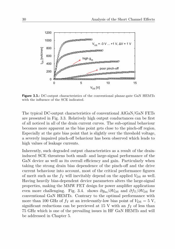
Figure 3.3.: DC-output characteristics of the conventional planar-gate GaN HEMTswith the influence of the SCE indicated.
The typical DC-output characteristics of conventional AlGaN/GaN FETsare presented in Fig. 3.3. Relatively high output conductances can be firstof all noticed in all of the drain current curves. The sub-optimal behaviourbecomes more apparent as the bias point gets close to the pinch-off region.Especially at the gate bias point that is slightly over the threshold voltage,a severely impaired pinch-off behaviour has been observed which leads tohigh values of leakage currents.
Inherently, such degraded output characteristics as a result of the drain-induced SCE threatens both small- and large-signal performance of theGaN device as well as its overall efficiency and gain. Particularly whentaking the strong drain bias dependence of the pinch-off and the drivecurrent behaviour into account, most of the critical performance figuresof merit such as the 𝑓T will inevitably depend on the applied 𝑉DS as well.Having heavily bias-dependent device parameters alters the large-signalproperties, making the MMW FET design for power amplifier applicationseven more challenging. Fig. 3.4. shows 𝜕𝑔m/𝜕𝑉DS and 𝜕𝑓T/𝜕𝑉DS forconventional GaN HEMTs. Contrary to the optimal performance withmore than 100 GHz of 𝑓T at an irrelevantly-low bias point of 𝑉DS = 5 V,significant reductions can be percieved at 15 V with an 𝑓T of less than75 GHz which is one of the prevailing issues in HF GaN HEMTs and willbe addressed in Chapter 5.

3.1. Drain Induced Short Channel Effects 31
Figure 3.4.: Behaviour of the peak transconductance (𝑔m) and intrinsic 𝑓T for conven-tional GaN HEMTs with respect to 𝑉DS.
Table 3.2.: Scaling properties with respect to device geometry and parameters of MMWHEMTs.
Device Geometry 𝐿g 𝐶gate 𝑑bar 𝐿gs
GaN10 technology 100 nm 0.5 pF/mm 11 nm 0.7 µm
Desired scaling trend ↓ ↓ ↓ ↓
Device Parameters 𝑔m 𝑅s 𝑅g 𝑅on
Planar deviceestimation
300–400mS/mm
0.4Ω·mm
30Ω/mm
1.2Ω·mm
Desired scaling trend ↑ ↓ ↓ ↓
Tri-gate deviceprediction
> 400mS/mm
0.4Ω·mm
35Ω/mm
0.8Ω·mm

32 Analysis of the Short Channel Effects
Keeping all this in mind, the adoption of the Tri-gate topology has re-cently been proposed [57] as a candidate approach to overcome the above-mentioned problems by means of suppressing the SCE. A higher modulationefficiency of the gate electric field in a Tri-gate FET is claimed to screenthe drain field to mitigate its impact, as several theoretical studies haveunveiled the promising scaling potential [59,60]. Being an essential part ofthe scope of this research, the effectiveness of GaN Tri-gate devices on thereduction of the SCE will be investigated in Chapter 4.
Table 3.2. summarises the rules for a successful device scaling towardsoperation in the MMW frequencies. The adoption of the Tri-gate approachis assumed to bring higher transconductance and on-resistance values withthe help improved gate controllability and saturated electron velocities,while the parasitics are predicted to remain unaffected.
3.2. Investigation of the Threshold Voltage
An indirect outcome of the SCE in highly-scaled GaN HEMTs is the unde-sired attribute of the threshold voltage. The conventional AlGaN/GaNdevices show a depletion-mode nature with considerably-negative thresh-old voltages as a result of the high 2DEG concentration formed at theAlGaN/GaN interface [43]. Often denoted as the normally-on mode of op-eration, such threshold characteristics cannot be considered as a preferableproperty in most applications where normally-off devices with a positive𝑉th are demanded.
On the other hand, the fact that the DIBL effect shifts the thresholdvoltage into the negative direction makes it even more challenging toachieve the normally-off operation. In addition to that, an aggressive gatelength scaling will amplify the negative shift due to the severity of theemerging SCE. The typical characteristics of the shift in 𝑉th and the DIBLare given in Fig. 3.5. in which the thickness of the AlGaN barrier is keptconstant.
With a decreasing gate length, the DIBL effect becomes increasingly morepronounced while the threshold voltage appears more negative in the samefashion. Particularly, below a certain gate length (around 200 nm in this

3.2. Investigation of the Threshold Voltage 33
Figure 3.5.: Simulated behaviour of the threshold voltage shift and DIBL over gatelength in conventional AlGaN/GaN HEMTs considering a constant barrier thickness.
case) the exponential behaviour of the 𝑉th shift approaches unacceptablevalues which points out the need of an according barrier thickness scaling.Nonetheless, it is also known that shrinking the barrier thickness too muchto compensate for the 𝑉th shift has a much more detrimental impact onthe gate leakage currents, concluding that the gate length scaling andthreshold voltage engineering towards the normally-off operation tend towork against each other.
3.2.1. Normally-Off Operation
In contrast to the nature of GaN-based HEMTs, it is necessary to achievethe normally-off behaviour for fail-safe operation in power electronics [4,6].DC-DC converter and inverter applications are two of the most criticalcases where the normally-off operation is highly-desired for reliable andlow-loss power switching. Moreover, the utilisation of enhancement mode(E-mode) transistors in logic or microwave circuits helps in the realisationof simplified bias networks [61–63].
Accordingly, a viable method towards normally-off GaN HEMT fabricationis considered to be the implementation of Tri-gate device architecture sinceits potential to effectively shift the 𝑉th has been presented by Ohi et al. [64].

34 Analysis of the Short Channel Effects
The positive threshold shift in Tri-gate FinFETs can be achieved throughimproved gate control over the 2DEG provided by the sidewall metallisationand partial strain relaxation within the formed narrow nano-channels. Theapproximation of the threshold voltage in typical AlGaN/GaN HEMTstructures can be given as [65]:
𝑉th ≈ ΦB − 𝜎pol,B
𝐶B− Δ𝐸C + Δ, (3.4)
where ΦB denotes the height of the Schottky barrier, 𝜎pol,B is the polarisa-tion difference between the barrier the buffer layers, 𝐶B is the capacitanceof the barrier, Δ𝐸C is the conduction band offset, and Δ is the conductionband well depth below the Fermi level. It is therefore clear that a reduc-tion in the piezoelectric polarisation or total polarisation charge, by eithershrinking the barrier or the width of nano-channels, leads to an increasein the threshold voltage.
The AlGaN/GaN FinFETs are also suitable to be combined with othertechniques in order to achieve higher positive threshold volatges. It hasalready been demonstrated in the literature that the normally-off can beobtained through several established methods including the gate-recessprocess [66,67], fluoride-based plasma treatment [68], adoption of a p-dopedGaN cap [69], or advanced multi-layer cap structures [70]. Since eachof the presented approaches have their own advantages and drawbacks,incorporating an appropriate method with the FinFET topology can boostthe effectiveness of the both.
In the gate-recess process the barrier layer under the gate can be thinnedin a selective fashion to deplete the 2DEG-channel which directly increasesthe 𝑉th. Whereas the plasma treatment approach benefits from the implan-tation of fluorine ions with a negative total charge into the barrier, leadingto a much higher threshold shift. On the other hand, the p-type doping ofthe cap permits normally-off operation by inducing negative space chargesin the depletion region with the help of an increased Schottky barrierheight. In the light of all the given information, the design of normally-offGaN HEMTs will be presented in Chapter 4.

3.2. Investigation of the Threshold Voltage 35
3.2.2. Integration of E/D Mode HEMTs
As far as the FET logic circuits are concerned, it is crucial to be able tomonolithically integrate D- and E-mode devices in various logic applicationsfor full functionality. Hence, it remains to be one of the most vitaltasks to enact the E-mode in highly-scaled GaN HEMTs in order tofully benefit from very high switching speed capabilities in mixed-signalcircuits. Once the normally-off GaN devices are made available, low-powerlogic applications will benefit greatly from the density advantage of GaNin a variety of circuits such as the direct-coupled FET logic (DCFL)topology [71].
Besides the high-speed logic circuits, the cooperation of normally-on andnormally-off devices will be advantageous in power electronics applicationsas well. The cascode driver configuration can be given as one of theexamples where E- and D-mode device integration would be beneficial forpower switches. Especially when the high-voltage operation is in question,the use of cascoded transistors is preferred. In which case a conventionalnormally-on high-voltage HEMT can be employed as the load device whilea normally-off device acts as a driver. The fact that the E-mode deviceis not required to withstand as high voltages as its D-mode counterpart,gives more degrees of freedom to achieve a better on-state performance byusing FinFETs. The schematic diagrams of the mentioned cascode driverand logic inverter device topologies are exhibited in Fig. 3.6.
Figure 3.6.: Schematic diagram of a sample (a) cascode power switch and (b) logicinverter configuration employing integrated E- and D-mode HEMTs.

36 Analysis of the Short Channel Effects
3.3. Chapter Conclusion
In this Chapter, the influence of the short channel effects on the device per-formance in highly-scaled GaN HEMTs were covered. Being an inevitableconsequence of an aggressive gate length scaling, the drain-induced para-sitic effects were investigated by means of analysing their impact on theon- and off-state characteristics of GaN HEMTs. It was ascertained thathaving a high DIBL was hazardous as the sub-threshold behaviour becamedeteriorated, both DC and HF performance parameters were diminishedas a result of an increased output conductance, and the threshold voltagecontrol was impeded which made the development of normally-off devicesmore challenging. Finally, it was proposed that the presented issues couldbe overcome by adopting the Tri-gate topology which exhibited the advan-tage of suppressing the SCE as well as it bore the potential to attain thenormally-off operation. In the following Chapter, design and developmentprocedures of the GaN Tri-gate HEMTs are covered with a focus on theinfluence of process variations on the essential device characteristics.

4. Design of GaN Tri-gateHEMTs
Due to its unique gate topology, the Tri-gate HEMT design requires amore sophisticated process flow than the conventional, planar-gate HEMTdesigns. The epitaxy, etching and deposition properties, passivation layerthickness and other critical process parameters need to be adequatelyoptimised as an inevitable consequence of the demanding mesa patterningof the active area. Accomplishing the optimisation of the Tri-gate devicegeometry then grants permission for the design of high-performance FETssuitable for MMW operation.
In this Chapter, the most critical aspects regarding the design and process-ing of Tri-gate devices will be discussed, with a focus on three-dimensionaldevice fabrication.
4.1. 3-Dimensional Device Fabrication
It is of crucial importance to be able to design and fabricate both con-ventional FETs with planar gates and Tri-gate FinFETs integrated onthe same wafer. Therefore, a specific process scheme has been developedthroughout this research, which is compatible with the existing planarFET fabrication technology of Fraunhofer IAF, by including additionalelectron beam (e-beam) lithography and mesa etching steps in order todefine and pattern the fin-shaped nano-channels, accordingly. The devicetopology of a FinFET differs from the conventional planar FET in sucha way that the gate electrode wraps around the nano-channels. Fig. 4.1.provides a visual comparison between the planar and Tri-gate FETs whererespective channel topologies are illustrated.

38 Design of GaN Tri-gate HEMTs
Figure 4.1.: Perspective-view illustration of (a) the planar-gate and (b) the Tri-gateFET indicating the fin-shaped nano-channels covered by the gate electrode.
The fundamental processing steps which have been established in thisresearch can be summarised as follows. The typical AlGaN/GaN het-erostructures, comprised of a 22-nm-thick Al0.22Ga0.78N barrier and grownon 300-µm-thick SiC substrates with a typical diameter of 3 inches, haveundergone mesa isolation as for the initial step of the device fabrication.The same mesa etching procedure, which was discussed in Chapter 2, hasbeen applied to both conventional and Tri-gate FETs. This is followed bythe formation of alloyed Ti/Al-based source and drain contacts on top ofthe crystal structure. The employed process scheme to form the ohmiccontacts on conventional AlGaN/GaN heterostructures includes the fol-lowing steps. Optical lithography step is first of all employed to define thearea of source and drain contact pads. This available lithography processdictates a minimum spacing between a contact pad and the gate foot of0.5 µm, assuming symmetrical gate-source and gate-drain spacings. Thenthe metal stack is evaporated comprising Ti/Al/Ti/Au which remainson top of the wafer specimen after the lift-off of the resist is performed.Rapid thermal annealing at temperatures around 800 – 850 ∘C is thennecessary to enable the diffusion of the metal stack into the barrier tocontact the 2DEG-channel. Nonetheless, when applied to more advancedwafer structures exhibiting lattice-matched InAlGaN or AlN barriers, thestandard annealing process gives rise to non-ideal Schottky-like ohmiccontacts. Hence, for the processing of those heterostructures, a contact
4.1. 3-Dimensional Device Fabrication 39
activation procedure involving Si-implantation has been developed whichwill be discussed in detail later on. It also needs to be noted that themetal stack undergoes a certain amount of lateral diffusion as a result ofthe annealing process which increases the surface roughness up to 0.2 µm.Therefore, in order to keep the transistor yield high enough the minimumgate-source distance has been set to 0.7 µm for all the devices that havebeen fabricated throughout this thesis.
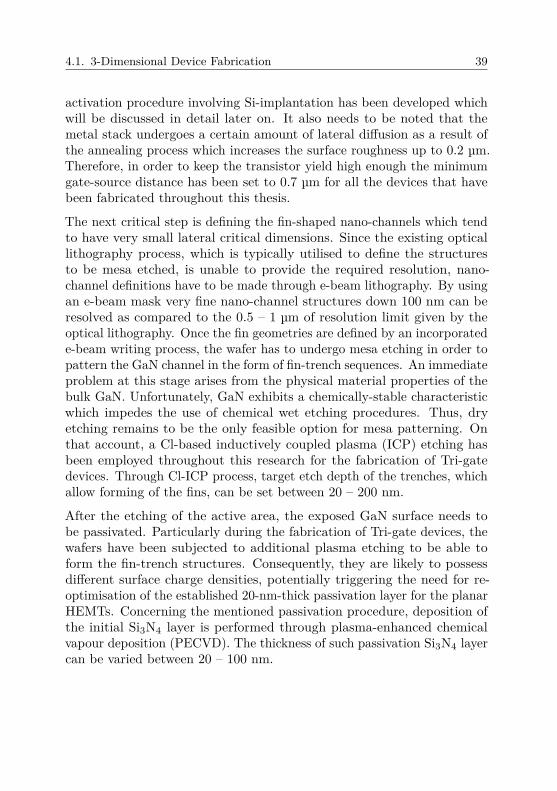
The next critical step is defining the fin-shaped nano-channels which tendto have very small lateral critical dimensions. Since the existing opticallithography process, which is typically utilised to define the structuresto be mesa etched, is unable to provide the required resolution, nano-channel definitions have to be made through e-beam lithography. By usingan e-beam mask very fine nano-channel structures down 100 nm can beresolved as compared to the 0.5 – 1 µm of resolution limit given by theoptical lithography. Once the fin geometries are defined by an incorporatede-beam writing process, the wafer has to undergo mesa etching in order topattern the GaN channel in the form of fin-trench sequences. An immediateproblem at this stage arises from the physical material properties of thebulk GaN. Unfortunately, GaN exhibits a chemically-stable characteristicwhich impedes the use of chemical wet etching procedures. Thus, dryetching remains to be the only feasible option for mesa patterning. Onthat account, a Cl-based inductively coupled plasma (ICP) etching hasbeen employed throughout this research for the fabrication of Tri-gatedevices. Through Cl-ICP process, target etch depth of the trenches, whichallow forming of the fins, can be set between 20 – 200 nm.
After the etching of the active area, the exposed GaN surface needs tobe passivated. Particularly during the fabrication of Tri-gate devices, thewafers have been subjected to additional plasma etching to be able toform the fin-trench structures. Consequently, they are likely to possessdifferent surface charge densities, potentially triggering the need for re-optimisation of the established 20-nm-thick passivation layer for the planarHEMTs. Concerning the mentioned passivation procedure, deposition ofthe initial Si3N4 layer is performed through plasma-enhanced chemicalvapour deposition (PECVD). The thickness of such passivation Si3N4 layercan be varied between 20 – 100 nm.

40 Design of GaN Tri-gate HEMTs
Afterwards, e-beam lithography is used once again to define the Ni/Pt/Au-based Schottky-gate electrode with the length of 𝐿g = 100 nm. Here, a T-shaped gate module has been selected which shows several advantages overconventional gate modules in terms of parasitic capacitances and processingdegrees of freedom. By using three separate resist layers with differentsensitivities the mentioned T-gate module can be created in a singlelithography step. In this case, the gate geometry becomes independentof the Si3N4 thickness and can be optimised by changing the thicknessof the resist layers. Moreover, parasitic contributions of the gate headcan be reduced as the T-gate process allows for increasing the height ofthe gate foot above 100 nm. Finally, the wafers are fully passivated by afinal Si3N4 layer while the transistors are already accessible for a completecharacterisation. Fig. 4.2. illustrates the resulting Tri-gate topology fromthe cross-section along the gate width and the proposed device geometryfrom the top view.
Figure 4.2.: (a) Cross-sectional schematic view of the nano-channel FinFETs and (b)illustration of the fabricated HEMT process.
Throughout the conducted experiments concerning the evaluation of GaNTri-gate HEMTs, relatively small-sized devices have been utilised to fa-cilitate fairer comparisons between the planar FETs and to isolate theeffect of gate width scaling. The transistor layout used for Tri-gate devicedevelopment and investigation is a well-established and straightforwardcommon-source (CS) HEMT design in coplanar waveguide (CPW) envi-ronment which is displayed in Fig. 4.3.

4.1. 3-Dimensional Device Fabrication 41
Figure 4.3.: Schematic layout of the CPW FET topology with 2 × 50 µm gate fingersand 50 µm of gate-to-gate pitch.
In this particular design the active area of the transistor constitutes only avery small portion of the entire device while the contact pads and partialCPW transmission lines occupy a significant amount of total surface area.This, in return, escalates the necessity to characterise and subsequentlyde-embed the parasitic elements (effective capacitances and inductancesof the pads) of the FET device. Moreover, the design of its active areais fairly compact as the gate bus is comprised of two symmetrical gatefingers, each having 50 µm of electrode width. The gate width is chosenso that the individual fingers are kept long enough to provide sufficientamplification to compensate the parasitics of the contact pads and therest of the passive components while, short enough to still maintain a highcut-off frequency. A gate-to-gate pitch of 50 µm has been established whichpresents a relatively relaxed physical conditions for thermal dissipationwithout affecting the frequency response too much.
Another advantage of the CPW FET topology is the fact that less timeand effort is required for the fabrication of fully-functioning devices withminimum number of process steps. Unlike the conventional full processof GaN circuits developed by Fraunhofer IAF which includes severalpassivation nitride layers, air bridges, via holes and metal stacks, only a

42 Design of GaN Tri-gate HEMTs
single metal layer (excluding the gate and ohmic contact metallisationlayers) is sufficient to define the layout of the transistor geometry. Thefabrication process can successfully be terminated after the deposition ofthe first metal stack where the CPW FETs are readily available to betested. Additionally, the use of separate ground planes eliminates theneed of a backside process of the wafers in which, deposition of a backsidemetallisation layer and through-wafer via holes are typically employed,following the thinning of the substrate material. Therefore, the completebulk SiC substrate can be kept under the device which assists a risk-freehandling of the wafer while providing reasonable thermal dissipation.
Following the fabrication of the first FinFET devices, a basic characterisa-tion has been followed to determine the DC performance of the first-passTri-gate HEMT design. Fig. 4.4. reveals the DC-transfer characteristicsof the Tri-gate devices fabricated by applying the initial process scheme.When compared to the typical planar GaN HEMTs discussed in Chapter 2,the achieved saturation current density of 550 mA/mm and the peaktransconductance of 150 mS/mm renders the performance of the first-passFinFET sub-optimal which requires extensive optimisation.
Figure 4.4.: Measured DC-transfer characteristics of first-pass Tri-gate HEMT designat 𝑉DS = 5 V (normalised to the metallurgical gate width).

4.2. Process Development 43
4.2. Process Development
In order to achieve the optimum GaN Tri-gate device performance, theexisting manufacturing scheme has to be improved by means of optimisingthe individual process parameters. Such process optimisation includesselection of the optimum device geometry, feasibly performing an effectivemesa etching of the active area and optimising the profile of the 3-Dpassivation layer sequence.
4.2.1. 3-D Mesa Nano-Channel Patterning
A crucial step which needs to be investigated regarding the Tri-gateHEMT fabrication is the patterning of the active area to form the nano-channels. As far as the Tri-gate principle is concerned, the channel hasto be partially etched all the way through the GaN cap, barrier, and intothe GaN buffer layer. Such selectively etching of the heterostructures in avery fine resolution essentially constitutes the major topological differencebetween the planar and Tri-gate HEMTs. Throughout this investigationthe mesa etching method, equipment and etch depth can said to be themain parameters to be optimised.
First of all, a decision on the method to mesa etch the wafers has to bemade. The selection of the etching method will have a tremendous impacton the device performance since it defines the surface and sidewall qualityof the channels. As mentioned in the beginning of this Chapter, the factof GaN being a chemically stable material rules out all of the wet etchingmethods. Hence, it is foremost important to carefully select the methodand equipment to perform the procedure since only dry etching can beused to pattern the GaN channel.
Once the GaN Tri-gate experiments in the literature are examined, itcan immediately be noticed that reactive ion etching (RIE) appears tobe one of the most prominent mesa etching methods. This method de-serves maximum attention since the bombardment of reactive ions mighthave detrimental effects on the nano-channel quality if not well-controlled.Some of the most widely-used dry etching methods for GaN Tri-gate in the

44 Design of GaN Tri-gate HEMTs
literature include transformer-coupled RIE with tetramethyl ammonium hy-droxide (TMAH) treatment [58,72–79], RIE assisted by electron-cyclotron-resonance plasma (ECR-RIE) [64,80–85], chlorine-based ECR-RIE [57,86],and Cl-based inductively-coupled plasma (Cl-ICP) [87–89].
In comparison, the Cl-ICP can be described as a relatively low-etch-rate process where minimum damage to the sidewalls of the formed finsis ensured. In contrast, majority of the previous studies report thatRIE brings along the need of lengthy wet etching treatment in order toeliminate the surface damages [90–95]. Whereas some groups argue thatthe level of crystal damage inflicted by the RIE is not high enough tobe concerned [64, 80]. In the light of all the available information anddue to its relatively safer nature, the Cl-ICP etching method has beenadopted in this work and all of the Tri-gate structures have been etchedthrough Cl-ICP accordingly. An additional benefit of this procedure is thepossibility to gain better control over the trench depth, given the relativelylower etch rates.
Determining the etch depth and therefore the height of the fin-shapednano-channels remains to be another critical investigation waiting to beaccomplished. For a successful Tri-gate HEMT design the heterostructuremust be etched at least beyond the barrier height to eliminate the 2DEGbetween nano-channels. In fact, the theoretical analysis of GaN Tri-gatesand device simulations suggest that keeping the fin height just abovethe total thickness of the cap and the barrier is sufficient for the desiredTri-gate operation [96,97]. Further etching deep into the GaN buffer wouldraise the issues of increased surface damage, trap density, and parasiticcapacitance which are all threats to the device performance. Despite theclear advantage of etching as shallow as possible in theory, experimentalresults might appear differently in practice due to process deviations andimperfections. One concern would be the uniformity of the etching process.Even though the Cl-ICP method is not the most aggressive procedure,there will be a certain amount of etch depth uncertainty to be taken intoaccount.
Regarding the experiment, the etch rate of the Cl-ICP equipment usedthroughout this work is given as 4 nm/s. Within the scope of this particularinvestigation the target etch depth of the mesa channels have been variedfrom 200 nm down to 25 nm. As for the initial experiment, 200 nm of

4.2. Process Development 45
target etch depth has been defined while forming the nano-channels of𝑊fin = 𝑊trench = 500 nm and 𝐿fin = 1 µm referring to the geometricalparameters shown in Fig. 4.2. (a). The first step of the optimisationprocedure then included reducing the etch depth to 100 nm, as well as the𝑊fin. Fig. 4.5. exhibits the scanning-electron-microscope (SEM) image ofthe array of the first 100-nm fin structures.
Figure 4.5.: Scanning-electron-microscope (SEM) image of the fin structures prior togate metal deposition and respective geometries depicted in the top inset.
Throughout the development of Tri-gate devices the etch depth has sys-tematically been varied parallel to the improvement of other processparameters. Following the first demonstration of 100-nm fins, furtherexperiments have been conducted with 50 nm and 25 nm of etch depths.Unfortunately, a fully-controlled etching experiment by keeping all of theremaining parameters constant would not be feasible. Accounting forthat, the performance of Tri-gate transistors within the experiments ofrespective etch depths have been directly compared to the co-fabricatedplanar transistors on the exact wafers. The dynamic drain current ratiobetween the on- and off-states (𝐼ON/OFF = 𝐼D,sat / 𝐼D,min) is considered tobe a good figure of merit for determining the switching performance. Sincethe 𝐼ON/OFF ratio defines the controllability of the channel, it becomes anespecially suitable indicator for the switching performance of Tri-gate. Forcomparison, the ratio of maximum saturation drain current density to the

46 Design of GaN Tri-gate HEMTs
drain leakage current density taken from the best FET samples on waferswith respective trench depths have been collected. The resulting 𝐼ON/OFFvalues achieved with respect to the etch depth are plotted in Fig. 4.6.
Figure 4.6.: Relation of the best achieved on/off performances in planar and Tri-gateFETs to the varied mesa etch depth.
The necessity of a relative comparison can clearly be acknowledged hereas the planar FETs show slightly fluctuating performances with 𝐼ON/OFFvalues ranging between 105 and 107 while the Tri-gate FETs exhibit a muchmore distinct correlation with the etch depth. At 200 nm, the 𝐼ON/OFFratio remains below 104 but then consistently rises with decreasing etchdepth until a superior performance of 𝐼ON/OFF = 108 is obtained at 50 nmwhen compared to the best planar result of 107. However, Once the depthis further reduced to 25 nm, the on/off performance once again falls behindof the planars, possibly due to the lost lateral control with such shallowtrenches. According to the overall results a target mesa etch depth of 50 nmcan said to be the optimum value for the best Tri-gate performance.
4.2.2. Investigation of 3-D Surface Passivation
One of the key factors directly affecting the GaN HEMT performance is thesurface passivation step of the fabrication process. As already explainedin Chapter 2, deposition of a sufficiently-thick layer of Si3N4 on top of

4.2. Process Development 47
the GaN crystal structure helps neutralising the surface states and greatlyimproves the device performance as well as the reliability. Typically forthe surface passivation of GaN HEMTs the Si3N4 layer is deposited onthe active channel by using PECVD. At the beginning of this work a firstnitride passivation layer of 20 nm had been established as the standardprocedure concerning MMW GaN FETs. After forming the completeT-gate module a second and thick nitride layer is then deposited on top tofully cover the entire structure. Fig. 4.7. sets display to the SEM imagetaken at the cross-section of a typical complete T-gate module fabricatedin the standard process.
Figure 4.7.: Cross-sectional SEM image of a typical 100-nm gate module with Si3N4passivation structure and air voids.
Being the principal property of a first Si3N4 passivation layer, it has to bethick enough to effectively passivate the surface states. On the other hand,relatively high dielectric constant of Si3N4 offers a potential threat to theHF performance since higher thickness values may lead to an increasein the parasitic gate capacitance. Regarding the topic of parasitics theadvantage of a T-gate module is the ability to form air voids following theinitial nitride deposition which can be distinguished in Fig. 4.7. Thosevoids can lower the effective dielectric constant and parasitic capacitancesto preserve the HF performance.

48 Design of GaN Tri-gate HEMTs
Accounting for the conventional planar FETs, a nitride thickness of 20 nmserves as an optimum compromise between passivated surface states andparasitic gate capacitance. Howbeit, as a consequence of additional mesachannel etching, Tri-gate devices are expected to show different surfacestate properties and therefore require an altered passivation approach.Alternatively, thin layers of Al2O3 have recently been reported for the Tri-gate passivation [98] although, its higher dielectric constant may increasethe parasitic capacitances due to which, the Si3N4 is kept as the passivationmaterial in this work. Similar to the mesa patterning investigation, semi-controlled experiments have been carried out to optimise the passivationnitride thickness ranging between 20 – 100 nm which will be discussed indetail below.
Unlike the planar FETs, in which surface states on the polar (0001) plane(also denoted as the c-plane) is the only concern, other polar planessuch as the a- and m-planes as well as the semi-polar planes are alsopartially exposed in Tri-gate FETs. Additionally, etching through the bulkGaN exposes the sidewalls of the barrier structure as well, which makesthe passivation of all these surfaces a complex challenge. Once again,a comprimise has to be made between the surface states and parasiticcapacitances when passivating the Tri-gate structures. On that account,ensuring proper coverage of the passivation nitride on 3-D fin structuresbecomes critical while keeping the gate capacitance low enough.
Therefore a novel passivation scheme has been developed by means ofdepositing the nitride at the sidewalls of the fin-shaped nano-channelssince studies on FinFETs have already pointed out the adverse effects ofthe etching damages at the sidewalls [99]. In this approach, the interfacequality as well as the gate capacitance has been improved through sidewallpassivation. Namely, a 50-nm-thick Si3N4 isolation layer is first of alldeposited by PECVD, followed by an additional 20-nm layer covering thesidewalls of the fins. In this case the Schottky contact is only allowed atthe top-surface of fin channels after the deposition of the gate metal. Theexperimental results in Chapter 5 will provide a better insight on the effectof this passivation scheme on the HF Tri-gate device performance.

4.2. Process Development 49
Figure 4.8.: Compared DC-transfer characteristics of the first-pass (black curves) andthe optimised (red curves) Tri-gate HEMT design measured at 𝑉DS = 5 V (normalisedto the metallurgical gate width).
After the process optimisation of the Tri-gate devices, the achieved DC-characteristics have been compared to those of the initial Tri-gate HEMTdesign which are exhibited in Fig. 4.8. According to the measurementresults the 𝐼D,sat has been successfully increased to more than 800 mA/mmin contrast to around 550 mA/mm that was obtained with the first-passdesign. Similarly, a significant boost in the peak 𝑔m has been establishedwhich rises up to of 275 mS/mm. Thereupon, being an integral part of theprogress towards enhancing the overall device performance, optimisationof the process parameters have shown considerable improvements in theDC figures of merit.
Finally in relation to the 3-D surface passivation, the dispersion behaviourof the Tri-gate FETs needs to be inspected, for which, pulsed-DC measure-ments have been performed. Both gate and drain supplies are shaped bypulses having 1 µs of pulse width (with 𝑉DS,off = 15 V in the hot pinch-offand 𝑉DS,off = 0 V cold pinch-off state). The resulting pulsed output curvesare compared in Fig. 4.9. It can be said that both planar and Tri-gateHEMTs show comparable slight-dispersive behaviour in which the pulseddrain current densities drop to as low as 𝐼D,pulsed = 0.75 × 𝐼D,sat in theextreme case of hot pinch-off states.

50 Design of GaN Tri-gate HEMTs
Figure 4.9.: Pulsed DC-output characteristics of (a) planar and (b) Tri-gate HEMTsin hot pinch-off and cold pinch-off states with 𝑉GS,off = -7 V (normalised to themetallurgical gate width).
4.3. Design Aspects of the Tri-gate FETs
Until this point, the optimisation procedure of several process parametersand their outcome have been presented. Those investigations are vitalcomponents of a successful device development in order to achieve a goodbase performance out of Tri-gate GaN HEMTs. Even though the processdevelopment is inevitable, solely concentrating on the fabrication procedure

4.3. Design Aspects of the Tri-gate FETs 51
is not sufficient to guarantee optimum Tri-gate performace. Designingsuitable FETs which can fully benefit from the prospective advantages ofthe novel FinFET technology is proven to be equally important. Amongmany design aspects to be considered, it is necessary to investigate andoptimise the geometry of the Tri-gate channel, appropriately scale thetransistor in order to design high-performance MMW FETs overcomingthe short channel effects, and engineer the threshold voltage for the desirednormally-off operation. An illustration of the nano-channels in the Tri-gatedesign, alongside with the coupling effects are given in Fig. 4.10.
Figure 4.10.: (a) Illustration of the fin-shaped nano-channel geometry and the couplingeffects within Tri-gate HEMTs.
4.3.1. Device Geometry Considerations
In order to achive the best MMW performance by driving the GaN Tri-gatetechnology to the limits of its potential, the geometrical parameters ofthe FETs need to be optimised first of all. Considering that the Tri-gatedevice consists of an array of nano-channel structures, optimisation of thedevice geometry corresponds to determining the optimum dimensions ofthe individual fins within the nano-channels. Concerning the etch depth ofthe channel, in other words the height of the fins, a process optimisation hasbeen concluded as presented in the previous Section. Once the optimumdepth/height of the trench/fins are determined, other degrees of freedomin terms of transistor design are left to be improved.

52 Design of GaN Tri-gate HEMTs
One of the design parameters can said to be the length of the nano-channels, namely the 𝐿fin as depicted in Fig. 4.2. (b). Fig. 4.11. (a)illustrates the remaining parameters of the Tri-gate HEMT geometry whileFig. 4.11. (b) ehxibits an SEM image of the FET design as well as across-sectional view of the fin array obtained through focused-ion beam(FIB) imaging. Apart from the fin length, the width of the fins (𝑊fin) andtrenches (𝑊trench) appear to be the most critical parameters that requireoptimisation.
Figure 4.11.: (a) Illustration of the Tri-gate fin structure geometry at the cross-sectionand (b) SEM image of the Tri-gate device as well as the fin-shaped nano-channelsindicated underneath the Schottky-gate electrode in the bottom inset.
The variation of the 𝐿fin raises two major issues to be taken into account.To begin with, the length of the nano-channels will have a direct influenceon the area of the access region. Assuming that the spacing betweensource and drain contacts are kept constant during the investigation ofdifferent 𝐿fin, the access resistance is expected to be affected since thefins will occupy a variable portion of the total active area. It has alreadybeen shown by Arulkumaran et al. [114] that the electron velocity innano-channel GaN HEMTs is greatly influenced by the in-plane tensilestress component hence, 𝐿fin variation may lead to significant changes inthe electron velocity in the channel and alter the maximum saturationcurrent density of the device. On the other hand, perforating the channelin the form of such narrow fins can induce partial strain relaxation to giverise to different piezoelectric polarisation properties and electron transport

4.3. Design Aspects of the Tri-gate FETs 53
mechanism. Depending on the effect of fin length on the electron velocity,it may result in either increased or decreased saturation drain currentdensity 𝐼D,sat.
In that regard, Tri-gate devices have been fabricated with varied 𝐿finbetween 100 nm and 1000 nm. All of the remaining design and processparameters have been kept constant in order to isolate their respectiveinfluences on the performance. Therefore all structures have been grownon top of the initial epitaxy variant with a 22-nm Al0.22Ga0.78N barrierwhich was described earlier. The transfer characteristics of each Tri-gateFET variation with respect to 𝐿fin can be inspected in Fig. 4.12.
Figure 4.12.: DC-transfer characteristics of Tri-gate HEMTs with varied 𝐿fin measuredat 𝑉DS = 5 V (normalised to the metallurgical gate width).
It should be noted here that the fabricated FETs exhibit a total gateelectrode width of 100 µm consisting of two symmetrical gate fingersof 50 µm. Concerning the current density calculations, the total gatewidth normalisation is done with respect to the total metallurgical widthof the mentioned gate electrodes (𝑊g = 100 µm). This conventionalmethod, which has also been employed for gate width normalisation of theplanar FETs, provides a clearer insight on the extracted device parameters.Conversely, another normalisation method which has been commonly-usedfor Tri-gate devices in the literature takes only the effective 2DEG widthinto account. In that case the devices are normalised with respect to thecumulative gate widths of the individual nano-channels resulting in an

54 Design of GaN Tri-gate HEMTs
effective width of 𝑊eff = 𝑛 × 𝑊fin, where 𝑛 is the number of nano-channelsand 𝑊fin is the width of an individual fin-shaped nano-channel. The lattermethod, however, neglects the influence and parasitics of the trench regionsthus, the first method has been applied for the devices in this Subsection.
The resulting DC-transfer characteristics of the Tri-gate FETs have revealeda decisive impact of the 𝐿fin on both the 𝐼D,sat as well as the thresholdvoltage (𝑉th). Considering that the test structures possess 700 nm ofsymmetrical gate-source and gate-drain spacings (equalling to a constantdrain-source distance of 𝐿ds = 1.5 µm), the 𝐿fin = 1000 nm variant occupiesa significant amount of the total access region. Whereas the 𝐿fin = 100 nmvariant only overlaps the length of the gate electrode and does not extrudeneither of the access regions. According to the results considerable shiftsin the 𝑉th have been recorded in Tri-gate devices with a longer 𝐿fin. Aslow as -1.2 V of 𝑉th has been obtained by the FinFET with 𝐿fin = 100 nmwhereas the threshold increased to -0.3 V, -0.2 V, and 0 V for 𝐿fin =200 nm, 500 nm, and 1000 nm respectively. The increase of the 𝑉ththerefore signifies that the 2DEG within the fins becomes more depletedwith longer mesa etching of the trenches. It is also evident that the mostsignificant 𝑉th shift of 0.9 V can be achieved by merely extending thetrenches (i.e. 𝐿fin = 200 nm variant) into the access regions from a gate-foot-overlapping state. Further increasing the 𝐿fin by another factor of 5results in only a minimal shift in the threshold.
On the other hand the maximum achievable 𝐼D,sat has consistently beenreduced with increasing fin length. In the variant with the shortest finlength of 100 nm, over 800 mA/mm of 𝐼D,sat can be achieved. Once thefin length is stretched into the access regions, the absolute maximum𝐼D,sat begins to be strictly limited to 550 mA/mm and 380 mA/mm for𝐿fin = 200 nm and 500 nm respectively. In the extreme case of 𝐿fin =1000 nm, only 200 mA/mm of 𝐼D,sat becomes available. This reductionof the on-state DC performance can be associated to the induced partialrelaxation due to the aggressive mesa etching which would be in accordancewith the encountered shift in 𝑉th. Even though this shift appears to be anadvantageous feature clearing the path towards normally-off GaN HEMTs,the drop in saturation current has to be overcome in order to make it afeasible approach.

4.3. Design Aspects of the Tri-gate FETs 55
Together with the variation of 𝐿fin the width of the nano-channels, namelythe 𝑊fin, is also an important design parameter that needs to be in-vestigated regarding the geometry of Tri-gate devices. Having seen theinfluence of 𝐿fin on the drain current and the 𝑉th, varying the 𝑊fin may helpelucidate the conduction mechanism of the nano-channels and theassociated depletion profiles. For that reason FinFETs with 𝑊fin =500 nm and 100 nm have been fabricated keeping the 𝐿fin fixed at 1000 nmand the respective DC-characteristics have been analysed. Fig. 4.13. ex-hibits the behaviour of the transconductance for each device in whichthe resulting effect can be identified more clearly. For comparison, themeasurement result of a Tri-gate device with a shorter 𝐿fin = 500 nm isalso included.
Figure 4.13.: Transconductance behaviour of Tri-gate HEMTs with varied 𝑊fin at fixed𝐿fin = 1000 nm and 500 nm measured at 𝑉DS = 5 V (normalised to the metallurgicalgate width).
As the 𝑊fin is made to be reduced from 500 nm to 100 nm, more significantpositive shifts in the 𝑉th have been obtained when compared to the influenceof the 𝐿fin variation. As much as 2 V of 𝑉th increase has been enabledby the Tri-gate FETs with narrower fins. More importantly, notableimprovements in the linearity of devices have been achieved with a lowerratio of 𝐿fin / 𝑊fin as the 𝑔m has become much flatter with respect to thebias voltage. In case of 𝑊fin = 100 nm and 𝐿fin = 1000 nm a peak 𝑔m of150 mS/mm occurs at +0.9 V of 𝑉GS. For the HEMT with a shorter 𝐿finof 500 nm the corresponding 𝑉GS at peak 𝑔m of 175 mS/mm gets deviated

56 Design of GaN Tri-gate HEMTs
to +0.5 V however, remains above 150 mS/mm over a larger portion ofbias range from -0.5 V up to +1.7 V. Similarly, a reasonably flat 𝑔m profilecan also be noticed in the 𝑊fin = 500 nm, 𝐿fin = 1000 nm variant wherearound 200 mS/mm of peak 𝑔m occurs earlier at 𝑉GS = -0.8 V.
When subjected to a cross comparison with the DC performance charac-teristics of the conventional planar FETs, it is evident that the Tri-gatedevices at their initial state of optimisation have fallen behind that of theplanars in overall performance which typically feature over 1 A/mm of𝐼D,sat and up to around 400 mS/mm of peak 𝑔m. Despite this, each varia-tion of device geometry bears the potential to improve the performanceof a respective figure of merit. Namely an increased 𝐿fin in combinationwith narrow 𝑊fin promises to be highly-beneficial towards normally-offoperation with a shifted 𝑉th into the positive gate bias. Minimising the 𝐿finon the other hand flattens the 𝑔m behaviour which is a desired propertyfor linear power amplifier applications.
Since decreasing the fin width and increasing the fin length shifts thethreshold voltage 𝑉th of Tri-gate devices in the positive direction, it bringsthe onset of the Schottky-gate and the forward gate currents into question.Even at 𝑉GS = 3 V the drain current still appears to be in an increasingtrend for most FinFETs. Bringing the FET operation in such high positivegate voltages bears the risk of facing the forward Schottky-gate current asa potential limiting factor. Collectively, all Tri-gate variants with different𝐿fin are once again measured and the corresponding gate current (𝐼G)behaviour have been depicted in Fig. 4.14. Having comparable Schottkybarrier heights (ΦB) of between 0.9 eV and 1.1 eV, the devices have shownsharp raises in the 𝐼G up to 10 mA/mm at a measured drain bias point of𝑉DS = 5 V.
In order to unveil the behaviour of the gate currents, a thorough investiga-tion and a comparative analysis of the forward Schottky onset of FETs atdifferent 𝑉DS must be carried out. For a fair comparison, the same testFETs (both planar and Tri-gate) with 100 µm (2 × 50 µm gate fingers)of total gate width have been analysed. Again, no specific gate widthnormalisation method has been performed in the presented results for theTri-gate transistors and therefore a simple traditional normalisation hasbeen adopted for both planar and FinFETs taking the geometrical gateelectrode width of 𝑊g = 100 µm.

4.3. Design Aspects of the Tri-gate FETs 57
Figure 4.14.: Gate current (𝐼G) behaviour of Tri-gate HEMTs with varied 𝐿fin measuredat 𝑉DS = 5 V (normalised to the metallurgical gate width).
Accounting for the DC measurements, the behaviour of the gate current(𝐼G) has been recorded with respect to swept 𝑉GS taken at different drainvoltages namely at 𝑉DS = 0.1 V, 1 V, 2 V, 5 V and 15 V. The resultingabsolute values of 𝐼G in planar FETs as a function of 𝑉GS are plotted inFig. 4.15.
Figure 4.15.: Measured gate current behaviour of AlGaN/GaN planar HEMTs withrespect to swept 𝑉GS at varied 𝑉DS from 0.1 V to 15 V (normalised to the metallurgicalgate width).

58 Design of GaN Tri-gate HEMTs
According to the gate current results of the planar FETs, it is immediatelynoticed that the forward Schottky onset of the gate is effectively influencedby the applied drain voltage and shifted towards the positive directionwith increased 𝑉DS. Regarding the measurement at 𝑉DS = 0.1 V, theminimum 𝐼G = 0.2 µA/mm occurs at 𝑉DS = 0.1 V. The gate leakagecurrent then slowly increases in the low-current region with a relativelylow slope until the transition onset point (approximate Schottky barrierheight ΦB = 1.1 eV). From the Schottky-gate onset onwards, the currentrises with much a higher slope exhibiting a relatively low ideality factorclose to unity. In the resistance-limited high-current region, the idealityfactor begins to slightly increase only until the saturation is finally reachedabove 100 mA/mm. Once the drain bias voltage is increased to 𝑉DS =1 V, it can be seen that the Schottky-gate onset voltage also gets increased.The positive shift in the onset voltage is sustained with raised drain biasas it appears to be around 𝑉GS = 2.4 V at 𝑉DS = 5 V. Particularly in theextreme case of 𝑉DS = 15 V, the signs of Schottky onset have not beenencountered up to 𝑉GS = 3 V as the overall gate leakage current remainsconstantly above 50 µA/mm.
In order to collectively compare the onset shifts, two distinct referencethreshold currents can be defined at this point. The first reference thresholdis selected as 𝐼G = 1 mA/mm, being the most widely-accepted leakagecurrent limit. The second reference is selected as 𝐼G = 10 mA/mm, belowwhich the effect of gate leakage has negligible influence on device intrinsicparameters and gate parasitics, corresponding to approximately 1% of thesaturation drain current. Accordingly, the 1 mA/mm threshold is crossedat 𝑉GS = 1.4 V, 1.8 V, 2.25 V, and 3 V for 𝑉D = 0.1 V, 1 V, 2 V, and 5 V,respectively. The 10 mA/mm threshold is then crossed at 𝑉GS = 1.6 V,2.0 V, 2.4 V, and well above 3 V for 𝑉DS = 0.1 V, 1 V, 2 V, and 5 V,respectively.
Coming to the Tri-gate FETs, Fig. 4.16. exhibits the behaviour of 𝐼G as afunction of 𝑉GS for FinFETs with 𝐿fin = 𝑊fin = 𝑊trench = 100 nm. It canbe seen that the drain bias dependence of the Schottky-gate onset shift ismuch less pronounced when compared to the planar FETs. The differencesin both 1 mA/mm and 10 mA/mm reference crossing voltages appear lessthan 1 V even at up to 𝑉DS = 15 V. Again unlike the planars, the currentimmediately begins to rise with a high slope even in the low-current region.The increase in the ideality factor also occurs much earlier and stronger

4.3. Design Aspects of the Tri-gate FETs 59
Figure 4.16.: Measured gate current behaviour of AlGaN/GaN Tri-gate HEMTs withrespect to swept 𝑉GS at varied 𝑉DS from 0.1 V to 15 V (normalised to the metallurgicalgate width).
than the planars, having reached only above 𝐼G = 1 mA/mm. However,the high-current region behaviour and the current levels of Tri-gate FETsshow similarities with the planar FETs. In both cases and at high 𝑉DS,critical gate current levels for device parasitics (more than 1% of thesaturation drain current) are reached only at 𝑉GS of higher than 2.5 V.Fig. 4.17. sets display to an overall comparison between the planar andTri-gate gate currents as the key measurement results are superimposedon the same plot.
It has been verified that the increase in the applied drain bias voltage shiftsthe Schottky-gate onset voltage towards positive direction in AlGaN/GaNHEMTs. The shift is particularly pronounced in the planar-gate transistorswhereas the 𝐼G behaviour of Tri-gate devices show a more complex trend,likely due to the distinct Schottky interfaces of the gate metal stack atGaN and AlGaN with different barrier heights. On the other hand, thehigh-current region behaviour converges to that of the planars as thecritical 𝐼G thresholds are crossed at similar gate bias voltages.

60 Design of GaN Tri-gate HEMTs
Figure 4.17.: Superimposed gate currents of AlGaN/GaN planar (solid lines) and Tri-gate (dashed lines) HEMTs with respect to swept 𝑉GS at varied 𝑉DS from 0.1 V to15 V (normalised to the metallurgical gate width).
4.3.2. Suppression of the Short Channel Effects
Since the established planar transistors, intended for the use in MMWapplications, are highly-scaled with 100 nm of gate length, the conditionof a short channel is inevitably introduced. As a result of this, variousshort channel effects (SCE) become apparent which can be detrimental forthe HF performance of the devices. It can be asserted that an insufficientcontrol of the channel provided by the gate electrode only at the top ofthe channel causes the planar devices to severely suffer from SCE. Theuniform electric fields which surround the 2DEG in Tri-gate devices, onthe other hand, are expected to reduce SCE while providing better on-and off-state performance.
With the intention of suppressing the SCE, first of all the sub-thresholdcharacteristics of the AlGaN/GaN devices have been determined which canbe examined in Fig. 4.18. Having measured both the planar FET and all ofthe FinFET variants with different 𝐿fin the drain current behaviour havebeen recorded. According to the measurement results, an improved sub-threshold swing of 150 mV/dec is possessed by the FinFETs with reduceddrain leakage currents below 10 µA/mm This confirms a superior off-state

4.3. Design Aspects of the Tri-gate FETs 61
performance over the planar FETs with 350 mV/dec of sub-threshold swingand 30 µA/mm of leakage current.
Figure 4.18.: Measured sub-threshold characteristics of planar and Tri-gate HEMTswith varied 𝐿fin measured at 𝑉DS = 5 V (normalised to the metallurgical gate width).
Another indicator of the SCE can be observed in the form of drain inducedbarrier lowering (DIBL). In the presence of a short channel, mainly thelateral component of the electric field originating from the applied drainbias is considered to be responsible for the DIBL. This lateral electric fieldbegins to screen the vertical component exerted by the gate electrode anddestructively alters the pinch-off behaviour of the transistor.
Fig. 4.19. exhibits the comparison of DC-transfer characteristics betweenthe planar and Tri-gate FET of 𝐿fin = 100 nm variant taken at different𝑉DS. It can be seen that 𝑉th of the planar FET appears to be shifted intothe negative direction when 𝑉DS is increased which is a typical signatureof the DIBL. The corresponding DIBL in this case can be calculated as100 mV/V. The negative 𝑉th shift of the Tri-gate FET however is provento be much less severe, having a reduced DIBL of 30 mV/V. Thereforethe obtained results ascertain that the pinch-off behaviour of FinFETs aresignificantly less influenced by the electric fields introduced by the appliedvoltage on the drain side.

62 Design of GaN Tri-gate HEMTs
Figure 4.19.: Measured transfer characteristics of planar (dashed lines) and Tri-gate(solid lines) HEMTs with 𝐿fin = 100 nm at varied 𝑉DS from 1 V to 15 V (normalisedto the metallurgical gate width).
In the end, it can be concluded that the implementation of Tri-gate topologyholds the key for achieving excellent off-state GaN HEMT performanceby means of suppressing the SCE which results from an improved gatecontrol.
4.3.3. Design of Normally-Off HEMTs
A substantial outcome of the device optimisation procedure has beengaining a better understanding on the threshold voltage control by theTri-gate topology. The lateral and the vertical modulation of the fin-shapedchannels allows the threshold voltages of the designed transistors to beshifted into the positive direction, which has already shown great potentialto enable the enhancement-mode (E-mode) of operation. As alreadydiscussed in Chapter 3, significant challenges have to be overcome on theway of achieving normally-off GaN HEMT operation. Such challengesinclude maintaining high on-state currents and minimising the leakagecurrents to ensure an acceptable off-state performance.

4.3. Design Aspects of the Tri-gate FETs 63
The most commonly-used process methods for normally-off GaN devicefabrication include gate recess, plasma treatment or a combination ofthe two [5,66,68,70,100–103]. However, the on-resistance of the channeltypically increases in such devices while suffering from diminished on-state performance. Ever since the first demonstration of its positive𝑉th shifting capability [64], the FinFET topology have recently gainedsignificant attraction. Subsequently, E-mode GaN FinFET devices withnormally-off operation have been reported by several studies in eithermetal-insulator-semiconductor field effect transistor [57, 72, 73, 104, 105](MISFET) or Schottky-gate nano-channel configuration [87]. By takingthese points into account and by carrying out a dedicated optimisationprocedure, the normally-off GaN Tri-gate FETs have been designed andtheir performances have been evaluated throughout this work. In orderto serve as a guideline, Fig. 4.20. presents the expected 𝑉th behaviour atrespective Tri-gate channel geometry which points out that a certain degreeof strain relaxation is indispensable to be able to reach the normally-offoperation, given the 100 nm of minimum manufacturable fin width.
Figure 4.20.: Behaviour of the simulated threshold voltage with respect to the fully-strained nano-channel (fin) width in Tri-gate HEMTs.
As for the epitaxy, the optimised AlGaN/GaN heterostructure variantwith 11-nm-thick Al0.32Ga0.68N barrier and 2-nm-thick GaN cap has beenselected to fabricate the E-mode FinFETs on top. Targeting an etch depthof 50 nm, the e-beam-defined fins with 1.5 µm of 𝐿fin and 100 nm of

64 Design of GaN Tri-gate HEMTs
𝑊fin have been patterned. Since the DC-characteristics of the normally-offdevices are the main point of interest, an effective gate width normalisationmethod has been employed as the total effective gate width of the FinFETsare given by 𝑊eff = (TGW × 𝑊fin) / (𝑊fin + 𝑊trench) = 50 µm. Oneof the adverse effects of forming long fin-channels is the diminished on-state DC performance, as it has been investigated earlier. Consequently,relatively lower saturation drain current densities have been observed in thefabricated E-mode Tri-gate devices. In order to carry out a more systematicanalysis of the 𝑉th-shifted HEMTs by having comparable current levels tothe planar FETs, D-mode FinFETs have also been fabricated alongsidewith the E-mode devices. Contrary to the normall-off HEMTs, the D-modeFinFETs are comprised of truncated fin-shaped nano-channels as short as𝐿fin = 200 nm, offering only a limited positive 𝑉th shift. Resulting from thestrain-relaxation-induced reduction of the piezoelectric polarisation [80,106]together with the reinforced gate control by the lateral fields [64, 107] theE-mode FinFETs, which feature much longer fin-arrays covering the entiredrain-source spacing, further facilitate shifting the 𝑉th.
Figure 4.21.: Measured DC-transfer characteristics and transconductance of the planarFET, D-mode and E-mode FinFETs at 𝑉DS = 5 V (normalised to the effective, 2DEGgate width).
Fig. 4.21. reveals the DC-transfer characteristics of the planar FET,D-mode and E-mode FinFETs measured at 𝑉DS = 5 V. According tothe results, E-mode devices have reached a positive 𝑉th of +0.2 V with400 mA/mm and 330 mS/mm of 𝐼D,sat and 𝑔m, respectively, compared to

4.3. Design Aspects of the Tri-gate FETs 65
𝑉th = -1.6 V, 𝐼D,sat = 1300 mA/mm, and 𝑔m = 450 mS/mm of the planarFETs. The improvement of the transconductance linearity especially inthe D-mode FinFET demonstrates the suppression of the SCE which ismore evident in Fig. 4.22. where the sub-threshold current behaviour ofthe planar FET, D-mode and E-mode FinFETs are plotted.
Figure 4.22.: Sub-threshold characteristics of the planar FET, D-mode and E-modeFinFETs at 𝑉DS = 5 V (normalised to the effective, 2DEG gate width).
It can be depicted from the measurement results that planar devicesfeature an on/off current ratio of around 7 orders of magnitude with adrain leakage current of 80 nA/mm at a bias point of 𝑉GS = -3 V, 𝑉DS= 5 V. Concerning the sub-threshold swing, 200 mV/decade has beenextracted for the planar FETs, according to the measurements. Takingthe overall DC characterisation results into account, it can be claimedthat the planar devices are suffering from SCE due to the inadequategate control whereas the E-mode FinFETs not only provide the desirednormally-off operation, but also exhibit superior off-state performancewith reduced SCE. Having reached very low drain leakage currents of3 nA/mm (1 nA/mm being the noise floor/measurement limit of the testsetup), an on/off current ratio of 8 orders of magnitude has been achievedby the E-mode FinFETs. Furthermore, a very steep sub-threshold swingof 75 mV/decade has been demonstrated which is close to the theoreticallimit of 60 mV/dec given for AlGaN/GaN HEMTs.

66 Design of GaN Tri-gate HEMTs
The output characteristics of the E-mode FinFETs can be found inFig. 4.23., which once again confirms the current stability provided by thefin-channels while demonstrating a significantly low specific on-resistanceof 𝑅sp = 0.025 mΩ·cm2, thanks to the spreading effect of the current inthe access region [108,109]. Here, it needs to be noted that the 𝑅sp hasbeen calculated with respect to the effective 2DEG width. Even thoughthe value that is obtained by using a traditional gate width normalisationwould still appear higher than of the planar devices, it signifies that theaccess resistance seen by the nano-channels has been reduced.
Figure 4.23.: DC-output characteristics of the E-mode FinFET measured between 𝑉GS= 0 V and +1.5 V (normalised to the effective, 2DEG gate width).
Regarding the output characteristics, a successful pinching off can befirst of all observed for the measurement points at 𝑉GS = 0 V wherea very low drain leakage current (𝐼D,min) has been sustained. At itsmaximum, the 𝐼D,sat rises up to 400 mA/mm once the 𝑉GS is increasedto +1.5 V. In contrast to the planar FETs or even the D-mode variantof FinFETs, more than two-fold reduction (from 1300 mA/mm down to400 mA/mm) of the 𝐼D,sat can be explained by the increased total channelresistance due to partial strain relaxation, as already investigated in theprevious Section. Especially in this experiment the reproducibility of theimpact of trench mesa etching on the 2DEG has been verified. The flatbehaviour of the DC-output curves then indicates minimised intrinsic

4.3. Design Aspects of the Tri-gate FETs 67
output conductance (𝑔ds) as well as drain induced short channel effects,all of which will be thoroughly investigated in Chapter 5. Furthermore,its flatness at particularly higher drain bias voltages indicate improvedthermal behaviour which is in agreement with the FinFET theory andexperimental results reported by Tamura et al. [81, 110].
Regarding the breakdown behaviour of the E-mode devices, DC-outputmeasurements have been conducted at a fixed 𝑉GS = 𝑉th - 0.5 V (defininga strict off-state condition) and the drain leakage currents are recordedas seen in Fig. 4.24. The threshold drain leakage current, at which thebreakdown voltage (𝑉br) is calculated, is commonly-chosen to be either1 mA/mm or 100 µA/mm for the published GaN-based transistors inthe literature. Although, such high leakage currents do not happen tobe sufficient for power electronics applications. Thus, a more realisticthreshold of 10 µA/mm has been selected for the 𝑉br extraction.
Figure 4.24.: Drain leakage current and breakdown voltage characteristics of the E-modeFinFET measured up to 𝑉DS = 70 V (normalised to the effective, 2DEG gate width).
Under the above-mentioned conditions the E-mode FinFETs exhibited anextracted breakdown voltage of 𝑉br = 60 V which is superior to that ofthe planar FETs at 28 V. Since the 2DEG within such long fin structuresgets extremely depleted in this E-mode variation, weakening of the chargecarrier concentration is assumed to play a major role which allows thedevice to withstand higher electric fields before the leakage-current-defined

68 Design of GaN Tri-gate HEMTs
breakdown occurs. As a consequence, the improvement of 𝑉br becomespromising for use in power electronics considering the very narrow gate-drain spacing of 𝐿gd = 0.7 µm.
Table 4.1. summarises the comparison of the different parameters of interestfor respective devices to provide a better overview on the overall perfor-mances. Both on- (𝐼D,sat, peak 𝑔m) and off-state (𝐼D,min, sub-thresholdswing) figures of merit are compared to shed light on the influence ofTri-gate topology on the suppression of the SCE. Accordingly, enhancedoff-state DC performance parameters achieved by the FinFET devices,in combination with the less bias-dependent and uniform 𝑔m behaviour,prove great potential and room for optimisation. In addition to this, highbreakdown voltages are also promising for the power electronics with lowerDC-power consumption and for high-speed and dynamic range switchingin logic circuits.
Table 4.1.: Comparison of performance parameters of planar FET, D-mode and E-modeFinFETs (normalised to the effective, 2DEG gate width).
Device/Parameter
PlanarFET
D-modeFinFET
E-modeFinFET
𝐼D,sat [mA/mm] 1300 1350 400Peak 𝑔m [mS/mm] 450 620 330
𝑉th [V] -1.6 -0.4 +0.2Gate leakage [nA/mm] ≤ 50 ≤ 40 ≤ 3Drain leakage [nA/mm] ≤ 80 ≤ 40 ≤ 3
DIBL [mV/V] 60 20 10Sub-threshold swing [mV/dec] 200 80 75
𝐼ON/OFF 107 107 108
𝑅sp [mΩ·𝑐𝑚2] 0.02 0.01 0.025𝑉br [V] 28 45 60
At the end of the development process, it is concluded that E-modeAlGaN/GaN FinFETs with high performance are designed and realisedreaching positive threshold voltages. The fabricated normally-off FinFETs

4.4. Investigation of Heterostructure Variations 69
demonstrated superior sub-threshold behaviour as well as successfullymitigated short-channel effects with a high on/off current ratio of 108 ina direct comparison to the conventional planar devices. The proposeddevices also exhibit enhanced breakdown performance which promise greatpotential for use in digital logic, mixed-signal circuits, as well as for thenext-generation power electronics. At this point, it is also acknowledgedthat the most significant benefit of adopting the FinFET topology canbe distinguished in the form of highly-linear device parameters. It hasalready been demonstrated that the 𝑔m behaviour of the FinFET devicesare proven to be flatter throughout bias voltages. Consequently, a flatterfrequency response is expected to be maintained over a large range ofoperation bias, owing to the minimised SCE, which is subject to a detailedinvestigation in Chapter 5.
4.4. Investigation of Heterostructure Variations
4.4.1. Impact of the Barrier on Electrical Properties
The design of a proper epitaxial layer sequence plays a significant rolein the overall performance of Tri-gate devices, as much as it defines thescaling properties of both planar and Tri-gate HEMTs. Concerning thestate-of-the-art technology prior to the development of Tri-gate transistortopology, the AlGaN/GaN heterostructures have typically been grownon SiC substrates by using metal organic chemical vapour deposition(MOCVD).
At the beginning of this work, the established heterostructure of thewafers initially consisted of a 3-nm GaN cap layer, 22-nm Al0.22Ga0.78Nbarrier, 2-µm GaN buffer and 120-nm AlN layer. As previously discussed inChapter 2, for a successful scaling of GaN HEMTs in the MMW frequencies,the distance between the gate metal and 2DEG needs to be decreasedwhile reducing the gate length. This requirement unequivocally suggeststhat the barrier properties have to be optimised by means of reducing itsthickness first of all. In order to sustain the ratio of 10 between the gatelength and the barrier thickness, an AlGaN barrier of 𝑑bar = 11 nm has

70 Design of GaN Tri-gate HEMTs
been adopted in the optimised case. The thickness of the GaN cap layerhas also been decreased to 2 nm.
On the other hand, it has already been manifested in Chapter 2 thatthe electron concentration in the 2DEG will inevitably suffer due to theminimised 𝑑bar. Apart from the barrier thickness, its composition needs tobe altered as well, being one of the decisive factors on the HF performance.Namely, the Al-content of the AlGaN has to be increased to compensatethe reduction in the sheet carrier density (𝑛s) as a result of the decreased𝑑bar. In the optimised case, the Al-content of the barrier has been increasedto 32% which is sufficiently high to regain the 𝑛s in the 2DEG and notexcessively high at the same time to cause adverse effects such as increasedtrap density or cracking of the barrier. Cross-sectional illustration of thecomposition of the initial and optimised epitaxial layers can be depictedin Fig. 4.25.
Figure 4.25.: Cross-sectional epitaxial layer sequence of the (a) initial and (b) optimisedAlGaN/GaN heterostructures grown on SiC substrate.
As a result of the AlGaN barrier optimisation, considerable improvementsin the 2DEG mobility (𝜇0) and the sheet resistance (𝑅sheet) have beenobtained. Furthermore, the 𝑛s has also been almost fully compensatedowing to the maximised Al-content. In the initial heterostructure con-figuration with 22-nm-thick Al0.22Ga0.78N barrier and 3-nm-thick GaNcap the specimen exhibited 1 × 1013 cm−2 of 𝑛s, 1000 cm2/Vs of 𝜇0, and650 Ω/sq of 𝑅sheet. Whereas in the optimised case with 11-nm-thickAl0.32Ga0.68N barrier and 2-nm-thick GaN cap, the mobility and sheetresistance have been improved to become 1300 cm2/Vs and 450 Ω/sq,respectively, despite a slight reduction in the 𝑛s down to 0.8 × 1013 cm−2.The demonstrated electrical properties of the optimised structure already

4.4. Investigation of Heterostructure Variations 71
promote the development of high-performance Tri-gate FETs with highersaturation 𝐼D, peak 𝑔m, and subsequently higher 𝑓T and 𝑓max.
As much as the thickness and the composition of the AlGaN barrier playsa critical role in maximising mobility while minimising 𝑅sheet, similarly,the peak 𝑔m of a HEMT device is also very closely related to the electricalproperties of the barrier structure. In fact, for a short channel device theapproximate relation can be given as:
𝑔m ≈ 𝜀r𝜀0𝑣e
𝑑bar, (4.1)
where 𝜀r is the relative dielectric constant of the barrier, 𝑣e is the saturationvelocity of electrons and 𝑑bar is the barrier thickness. From a design pointof view of the conventional planar HEMTs, our degree of freedom is limitedto the 𝑑bar which is the only parameter that can be altered. However,even an aggressively scaled down barrier is unfortunately not adequateto maximise the 𝑔m. At this point the FinFET approach can be a viablesolution thanks to the improved gate control and reduced SCE.
DC-transfer and sub-threshold characteristics of the designed planarand Tri-gate HEMTs with an optimised AlGaN barrier are plotted inFig. 4.26. According to the results, Tri-gate devices reach over 2 A/mmand 750 mS/mm of 𝐼D,sat and 𝑔m, respectively, compared to 𝐼D,sat =1.3 A/mm, and 𝑔m = 450 mS/mm of the planar FETs. The uniformelectric fields surrounding the 2DEG at the fins improve the saturatedelectron drift velocities as a result of an enhanced carrier transport mecha-nism which is assumed to be the fundamental reason behind the increasein the drain current density according to Tamura et al. [81]. Moreover,a significant increase in the 𝑔m has been obtained as anticipated whichsignifies superior channel control over the planar-gate approach.
Although, the conventional AlGaN/GaN HEMTs typically suffer from afundamental drawback. The inherent tensile strain caused by the mismatchof the lattice constants between the barrier and GaN limits the chargedensity in 2DEG channel to be originated from spontaneous polarisation,due to the presence of persistent piezoelectric polarisation. This can beovercome by growing lattice-matched barrier structures which will induceenhanced spontaneous polarisation to maximise the sheet carrier density.

72 Design of GaN Tri-gate HEMTs
Figure 4.26.: Measured DC-characteristics of planar and Tri-gate AlGaN/GaN HEMTswith 𝐿fin = 100 nm at 𝑉DS = 5 V (normalised to the effective, 2DEG gate width).
In the scope of this research, more advanced barrier layers have beenutilised to a replace the standard AlGaN. In one of the variations, a nearlylattice-matched quternary In0.1Al0.55Ga0.35N with a thickness of 𝑑bar =10 nm has been used underneath a 3-nm GaN cap. A very thin (1.3 nm)AlN spacer layer is also apparent on top of the buffer layer in this case.In an alternative variation, a pure AlN barrier of 4 nm thickness hasbeen employed alongside with the same 3-nm-thick GaN cap. Accountingfor both variants, the thicknesses of GaN buffer and AlN spacer havebeen reduced to 1.5 µm and 100 nm, respectively. Fig. 4.27. shows thecomposition of the advanced heterostructures with quaternary and binarybarriers.
Concerning those non-conventional epitaxies, the most applicable growthmethod has to be selected by potentially altering the standard growththrough MOCVD. It can be noted that the layer thickness of classicalAlGaN barrier is typically large enough to tolerate the uncertainty of thedeposition thickness given by the MOCVD. This allows the AlGaN/GaNheterostructures to be grown with sufficient control. The structures withadvanced barriers on the other hand exhibit very thin layers down to a fewnanometres which require well-controlled growing conditions. Particularlythe thickness of the AlN barrier becomes highly critical since only a 4-nm-thick layer separates the GaN cap from the GaN buffer. Gaining such a

4.4. Investigation of Heterostructure Variations 73
Figure 4.27.: Cross-sectional epitaxial layer sequence of the heterostructures with (a)InAlGaN and (b) AlN barriers.
high control over the epitaxial growth can be provided by the molecularbeam epitaxy (MBE) method. Therefore the wafers with InAlGaN andAlN barriers have been grown by using an MBE system.
The adoption of advanced barrier compositions of either a lattice-matchedInAlGaN or a pure AlN layer yields even more significant improvements inthe 𝑛s and 𝑅sheet as opposed to the AlGaN barrier optimisation. Accordingto the Hall measurement results the 𝑛s has successfully been boosted upto 1.5 × 1013 cm−2 and 3.3 × 1013 cm−2 for InAlGaN and AlN cases,respectively. Additionally, very low 𝑅sheet values have been achievedas low as 310 Ω/sq for the InAlGaN and 170 Ω/sq for the AlN barrier.Table 4.2. provides a summary of the achieved electrical properties by theutilised heterostructures with respective barrier variations.
Table 4.2.: Electrical parameters of the grown heterostructures with different barriers.
Barrier/Parameter Al0.22Ga0.78N Al0.32Ga0.68N InAlGaN AlN
𝜇0
[cm2/Vs] 1000 1300 1350 1100𝑛𝑠
[cm−2] 1 × 10¹³ 0.8 × 10¹³ 1.5 × 10¹³ 3.3 × 10¹³
𝑅sheet[Ω/sq] 650 450 310 170

74 Design of GaN Tri-gate HEMTs
Fig. 4.28. reveals the measured DC-transfer characteristics of the planarand Tri-gate InAlGaN HEMTs. Accordingly, FinFETs have reached highersaturation current densities above 2 A/mm, compared to the 1.5 A/mmof the planar FETs. An improved and flatter 𝑔m response has once againshown by the Tri-gate topology with a peak value of 370 mS/mm whereasonly up to the 230 mS/mm has been reached by the planar devices. Ithas to be noted that the relatively low 𝑔m values are not comparableto the AlGaN/GaN variant since the epitaxial layer thicknesses havenot been fully optimised yet in the lattice-matched structures. On theother hand, the threshold voltage of the devices have considerably beenshifted into the negative direction due to the high spontaneous polarizationcharges introduced by the InAlGaN barrier. Consequently, being one ofthe prevailing issues in implementing lattice-matched heterostructures,relatively escalated leakage currents over 1 mA/mm have been observed,which is yet to be resolved with the help of future investigation.
Figure 4.28.: Measured DC-characteristics of planar and Tri-gate InAlGaN HEMTswith 𝐿fin = 100 nm at 𝑉DS = 20 V (normalised to the effective, 2DEG gate width).
Concerning the sub-threshold behaviour depicted in Fig. 4.29., highly-diminished sub-threshold swings have been exhibited by the planar FETsin excess of 2000 mV/dec and 3000 mV/dec at 𝑉DS = 5 V and 10 V,respectively. On the other hand, better off-state performance has beenprovided by the Tri-gate with 1500 mV/dec and 2000 mV/dec of sub-threshold swing at 𝑉DS = 5 V and 10 V, respectively. Furthermore, at high

4.4. Investigation of Heterostructure Variations 75
applied drain bias voltages, the leakage currents have observed to be lowerthan of the planars. Even though the planar devices can maintain around1 mA/mm of drain leakage current at 𝑉DS = 5 V, more than 6 timeshigher leakages are encountered as soon as the bias voltage is increasedto 10 V. It is therefore evident that at typical desired operation points of15 V or 20 V, the influence of the drain-sided electric field will bring theleakages up into the intolerable levels. Looking at the Tri-gate, the sameamount of bias increase induces just over a 2-fold rise in the leakages, from4 mA/mm to 9 mA/mm. The DIBL is another figure of merit indicatingthe superiority of FinFETs over the planar FETs. The measured levels ofaround 150 mV/V affirm the dominance of drain bias on the channel overthe planar-gate control. In comparison, the Tri-gate topology improvesthe 2DEG controllability, lowering the DIBL figures down to 50 mV/V.
Figure 4.29.: Measured sub-threshold characteristics of planar and Tri-gate InAlGaNHEMTs with 𝐿fin = 100 nm at up to 10 V of 𝑉DS (normalised to the effective, 2DEGgate width).
4.4.2. Development of High-Current Tri-gate HEMTs
Despite that the recent advancements in conventional planar-gate GaN-based HEMTs have resulted in very high device speeds through extensivescaling [111,112], the demonstrated device performances are still fallingbehind the predicted values concerning GaN material properties as a result

76 Design of GaN Tri-gate HEMTs
of the unresolved critical problems. The sub-optimal saturation currentdensity of GaN devices is considered to be one of the issues as the reportedresults in the literature are unable to match the theoretical figures [113].The unique transport properties of the Tri-gate approach helps overcomingthe short-channel limitations and enables very high-current GaN HEMTsto be developed.
At this point it has been determined that the epitaxy, on which theTri-gate devices are structured, plays a significant role in achieving highsaturation current densities. Exhibiting the lowest 𝑅sheet of 170 Ω/sqas a result of the highest sheet carrier density of 3.3 × 1013 cm−2 (seeTable 4.2.), the heterostructure variant with a 4-nm AlN barrier promisesto be the best candidate for boosted electron flow. In an attempt todevelop high-current devices, two variants of AlN/GaN HEMTs have beenfabricated featuring 100 µm and 300 µm of total gate width. Both FETshave the same effective gate width of 𝑊eff = 100 µm in spite of the longermetallurgical with of the gate electrode in the latter variant. This is aresult of the TGW normalisation since the 300-µm-wide FinFETs consistof 𝑛 = 1000 nano-channels with 𝑊fin = 100 nm and 𝑊trench = 200 nm.
Figure 4.30.: Measured DC-characteristics of planar and Tri-gate AlN/GaN HEMTswith 𝐿fin = 100 nm at 𝑉DS = 30 V (normalised to the effective, 2DEG gate width).
Fig. 4.30. indicates the measured DC-transfer characteristics of the planarand Tri-gate AlN/GaN HEMTs. The surface traps due to the minor etchingdamages of the sub-micron mesa patterns are assumed to be the reason

4.4. Investigation of Heterostructure Variations 77
behind slight fluctuations and noisy spikes that are evident in the DC-transfer curves of the FinFETs. According to the results, the planar FETsare able to achieve medium-level saturation current densities of 1.5 A/mm.In contrast, very high maximum current densities have been delivered bythe nano-channel FinFETs up to 3.8 A/mm. The achieved 𝐼D,sat value isone of the highest among all state-of-the-art GaN-based Tri-gate HEMTs,following the devices reported by Arulkumaran et al. [114,115]. It has beensuggested in the mentioned studies that up to two times higher electrondrift velocities than the planar can be achieved in FinFETs thanks to theadditional localised in-plane tensile stress exerted on the nano-channelswhich is induced by the 3-D passivation nitride. Since optical phononscattering rates and the effective electron mass (𝑚*) are the most decisivefactors on electron transport, a stress-induced reduction in the 𝑚* in theTri-gate channel may be responsible for such high saturation drain currentdensities. Here, it needs to be noted that the emerge of gate leakagecurrents has also been successfully prevented through the implementationof a sidewall Si3N4 layer during the AlN/GaN FinFET fabrication process.Since metal-insulator-semiconductor (MIS) interfaces are introduced atthe sidewalls of the fin structures, the leakage paths are eliminated atparticularly very high applied gate bias voltages.
Figure 4.31.: Measured DC-output characteristics of Tri-gate HEMTs with AlGaN andAlN barriers (normalised to the effective, 2DEG gate width).
Serving as a direct comparison of both heterostructures (namely withAlGaN and AlN barriers), Fig. 4.31. depicts the DC-output characteristics

78 Design of GaN Tri-gate HEMTs
of the Tri-gate HEMTs on respective wafers. It can immediately be noticedin the DC-output curves that the knee-voltages of the AlN/GaN devicesappear to be shifted. This undesired behaviour in the linear region is aconsequence of the Schottky-like source and drain contacts which haveunintentionally been grown on these wafers instead of ideal ohmic contacts.During the deposition and annealing of the Ti/Al-based metal stack, astandard procedure has been followed in order to keep it consistent withthe entire fabrication process of AlGaN/GaN devices. In return, the lack ofsufficient metal diffusion into the barrier resulted in such non-ideal ohmiccontacts. However, it is possible to overcome this condition on wafers withAlN barriers by implementing a different process scheme which involvesSi-doping.
In order to eliminate the formation of Schottky-like contacts the fabricationprocess of AlN/GaN devices has been optimised by means of adding animplantation step. Prior to the deposition of ohmic contacts, surfaceof the wafer has been doped with Si atoms which have been activatedsubsequently. As for the previous case, contact resistances (𝑅cont) inexcess of 10 Ωmm has been measured on the specimens with an AlNbarrier. Fig. 4.32. reveals the measured contact resistances on 4 differentAlN/GaN wafers that have undergone Si-implantation procedure. Theobtained values of 𝑅cont = 0.25 mΩmm up to 0.5 mΩmm on all sampleshave successfully proven the consistency of the applied process.
Figure 4.32.: Statistical plot of the measured contact resistances on AlN/GaN wafersamples with respective mean values indicated.

4.5. Analysis of the Thermal Behaviour 79
4.5. Analysis of the Thermal Behaviour
As much as the GaN HEMTs are capable of delivering high current levels,the thermal effects show up as a critical obstacle that can limit theperformance. With increasing dissipated power in the device, the adverseeffects of self-heating become more apparent as it leads to raised channeltemperature which deteriorates electron transport with reduced mobility.
Since very high saturation drain current densities at considerably high drainbias voltages have been reached in AlN/GaN FinFETs, thermal behaviourof the devices needs to be looked into. It has been manifested by Asubar etal. that GaN-based FinFETs are less prone to self heating than the planarGaN FETs, owing to the heat spreader effect provided by the Tri-gatestructures which reduces the thermal resistance of the device by 30% [110].In order to investigate this, on-wafer infrared thermography measurementshave been carried out to determine the active region temperatures andsubsequently calculate the thermal resistances. Keeping the backsidetemperature of the wafer constant at 40 ∘C, varied bias voltages havebeen applied to both planar and Tri-gate FETs to generate dissipatedpower while the spot temperature in the active area has been recorded.Accordingly, the thermal resistance (𝑅th) can be calculated as follows:
𝑅th = 𝑇C − 𝑇A
𝑉DS · 𝐼DS, (4.2)
where 𝑇C and 𝑇A are the channel and the ambient (backside) tempera-tures, respectively. In analogy to the equivalent circuit modelling, the2-finger FETs under test can be represented by the respective thermalheat sources (𝑃1, 𝑃2), thermal capacitance (𝐶th) together with the 𝑅th ofthe fingers which are shown in Fig. 4.33. Assuming the same generatedheat in all devices, additional parallel 𝑅th is expected to emerge in theTri-gate due to the hypothesised heat spreading effect of the surroundinggate electrode. Hence, the theory suggests that a lower total equivalentresistance contributes to a more robust thermal performance than theplanar FET.

80 Design of GaN Tri-gate HEMTs
Figure 4.33.: Thermal equivalent circuit of the 2-finger FETs with constant dissipatedpower.
Fig. 4.34. presents the respective 𝑅th extracted for the planar HEMT andTri-gate HEMTs with fixed 𝐿fin = 100 nm and varied 𝑊fin, 𝑊trench. For afair comparison, all transistors exhibit the same geometrical gate width of100 µm. Up to 2 W of DC power can be dissipated by the planar devicebefore reaching 60 K/W of critical thermal resistance whereas the Tri-gatevariant with 𝑊fin = 200 nm, 𝑊trench = 100 nm allows up to 2.4 W ofdissipated power. On the other hand, the variant with 𝑊fin = 100 nm,𝑊trench = 200 nm can only reach around 1 W due to its limited totalsaturation current. The results also point out that at a fixed dissipatedpower of 1 W the corresponding 𝑅th are extracted to be 51 K/W forthe planar, 58 K/W for the narrow-fin, and 43 K/W for the wide-finTri-gate FET. Around 15% of improvement in the thermal resistance ofthe optimised Tri-gate agrees with the theoretical analysis and conjecture,albeit slightly less than the predicted advancement.
Another critical point of interest can said to be the analysis of the channeltemperature rise among the FET variations. Therefore, temperaturereadings with respect to the position (along the source-drain path) havebeen taken in all devices at the same constant dissipated power of 1 W.The resulting distribution of the temperatures are illustrated in Fig. 4.35.where the position of the gate, as well as the source and drain contactsare also included.

4.5. Analysis of the Thermal Behaviour 81
Figure 4.34.: Extracted thermal resistances of planar and Tri-gate HEMTs with varied𝑊fin, 𝑊trench measured at 𝑇A = 40 ∘C.
At the spot where the peak temperatures are encountered (namely, underthe gate electrode), the planar FET have reached higher than 90 ∘C ofchannel temperature. The narrow-fin Tri-gate device have exhibited aneven higher peak temperature of 100 ∘C whereas the wide-fin variant havesuccessfully maintained it under 80 ∘C.
An equally noteworthy outcome of this experiment is uniformity of thetemperatures among the two gate fingers. A considerable asymmetry isevident in the planar FET with more than 10 K of peak temperaturedifference between the gate fingers. Conversely, regardless of the fin width,both Tri-gate FETs have shown highly-symmetrical temperature profiles.As much as the reduced temperatures in the wide-fin variant can beattributed to the large surface area provided by the gate electrode aroundthe source of heat (2DEG channel), the ascertained temperature uniformitymight be an assisting factor.
In the end, the analysis have shown that the geometry of the fins sig-nificantly affects the thermal resistance in the Tri-gate channel. It hasbeen verified by the experimental results that an optimum Tri-gate designsuccessfully accommodates superior thermal performance by minimisingthe 𝑅th which reinforces high-power capabilities.

82 Design of GaN Tri-gate HEMTs
Figure 4.35.: Measured distribution of the temperatures in 2 × 50 µm devices at adissipated power of 1 W.
4.6. Chapter Conclusion
The development of a 3-D GaN Tri-gate device processing scheme, optimi-sation of the design parameters for an improved base performance, andthe analysis on the influences of advanced heterostructures was presentedin this Chapter. In order to exploit the full potential of GaN Tri-gateHEMTs in terms of essential properties such as current drive capabilityand low-leakage operation, geometrical parameters of the fin-shaped nano-channels were optimised. Concerning the fabrication of Tri-gate devices,peculiar process steps were established while assessing advanced epitaxialbarrier structures for an enhanced performance. It was also demonstratedthat the optimised FinFETs effectively suppressed various SCE such assub-threshold swing, DIBL, and output conductance. Through enabling apositive threshold voltage shift, normally-off Tri-gate FETs were demon-strated which promised beneficial features towards use in power electronicsand high-speed switching applications. Moreover, thermal properties ofthe Tri-gate FETs were analysed which shed light on the mechanismsresponsible for the improved on-state performance with high 𝐼D,sat at highbias voltages.

4.6. Chapter Conclusion 83
Building upon the existing GaN process scheme of Fraunhofer IAF, addi-tional e-beam and ICP mesa etching steps were utilised in order to formthe Tri-gate nano-channels with the least surface damage possible. Theestablished half-process allowed for the fabrication of functional Tri-gateFETs in a more time- and cost-efficient way than the full-process, aimed fora quick characterisation of the test devices. An initial process and devicegeometry optimisation proved feasibility of the sub-micron-scaled FinFETswith very high on/off performance (𝐼ON/OFF >108) and and minimisedSCE (75 mV/dec of SS, 10 mV/V of DIBL). The normally-off operationwas also established through threshold voltage engineering which resultedin the fabrication of E-mode devices (fully-integrated with the D-modeGaN FinFET technology) with 𝑉th = +0.2 V and 𝑉br = 60 V. Finally, theemployment of an AlN barrier in the Tri-gate heterostructure producedrecord saturation current densities as high as 3.8 A/mm with the help ofimproved thermal performance of the FinFETs.
The achievement of a successful Tri-gate HEMT fabrication process andthe improved DC-performances invoke the need for characterisation andmodelling in the RF regime. Therefore the investigation of small- andlarge-signal performances of both planar and Tri-gate devices in the MMWfrequencies are subject to the next Chapter.


5. Millimetre-Wave Performanceof Tri-gate FETs
It has already been demonstrated that a properly-optimised FinFET designholds key towards improving the performance of GaN-based HEMTs byexploiting the benefits of the Tri-gate topology. As much as the enhance-ments in basic electrical properties have been established, determining thebehaviour of the parasitics and SCE with respect to design parameters andgeometries remains as one of the prime issues that needs to be resolved.
This chapter will shed light on the influence of the most critical deviceparameters to evaluate the overall performance of GaN Tri-gate HEMTsin the MMW applications. To begin with, the investigation of parasiticgate capacitances and SCE will provide the guidelines to minimise them.Bias-dependence of small-signal figures of merit are then examined, leadingto the design of Tri-gate devices with high gain and linearity. Finally,the development of FETs suitable for MMW PAs with high RF outputpower will be enabled through analysis and optimisation of large-signalcharacteristics.
5.1. RF Characterisation of Tri-gate HEMTs
The MMW characterisation of the Tri-gate devices is necessary at this pointas it is crucial to be able to examine their applicability to the intendedapplications. Since the HF parasitics of the FETs emerge as the mostcritical limiting factor for the MMW performance, a complete investigationhas been conducted by taking small-signal S-parameter measurementsfollowed by the modelling of the intrinsic transistor. An equivalent circuitmodel can be used to represent the device and to subsequently extract

86 Millimetre-Wave Performance of Tri-gate FETs
the intrinsic parameters once the extrinsic components are accuratelyde-embedded.
Concerning the parasitics investigation of the 2 × 50 µm Tri-gate devices,on-wafer S-parameter measurements are performed up to 110 GHz byusing HP 8510XF vector network analyser and the small-signal parametersare extracted by employing the 3-D FET model [116] which is illustratedin Fig. 5.1. RF performances and particularly the parasitic capacitances ofFinFETs with varied Tri-gate topologies are then compared to the planarFETs. The equivalent circuit model consists of 8 discrete elements withinthe intrinsic shell as well as gate, drain, and source series resistancesattached to respective ports. In order to successfully fit the model tothe behaviour of the actual transistor, the extrinsic elements such as thecontact pads and capacitances between the 3-D structures have to be de-embedded. While the intrinsic parameters are functions of the bias point,the extrinsic elements are essentially passive components which allows themto be determined through electromagnetic field simulations. For the case ofTri-gate FET modelling a comprehensive multi-port 3-D model, includingthe pattern of fin-shaped nano-channels, has been prepared within HFSSCAD environment and field-simulated up to 110 GHz. It is then usedto de-embed into the intrinsic device reference plane when applied tothe raw S-parameter measurement data. In the end, the extraction ofthe individual elements of the circuit model is made possible by usingapproximate equations involving the Y-parameters.
Figure 5.1.: (a) 3-D field-simulated illustration of the nano-channels and (b) small-signal equivalent circuit model of the Tri-gate HEMTs depicting the intrinsic parasiticelements.

5.1. RF Characterisation of Tri-gate HEMTs 87
Having converted the resulting S-parameters of the FET model into cor-responding Y-parameters the intrinsic capacitances can be derived byapplying the following formulas:
𝐶gs = Im(𝑌11 + 𝑌12)2𝜋𝑓 (5.1)
𝐶gd = 12𝜋𝑓 · Im(−𝑌12) (5.2)
𝐶ds = Im(𝑌22 + 𝑌12)2𝜋𝑓 (5.3)
The input and output conductances can also be derived as follows:
𝑔gs = Re(𝑌11) − Re(−𝑌12) (5.4)
𝑔ds = Re(𝑌22) − Re(−𝑌12) (5.5)
Finally, the parameters of intrinsic transconductance and gate-drain resis-tance can be calculated as:
𝑔m = Re(𝑌21) (5.6)
𝑅gd = Re(−1𝑌12
)(5.7)
By the nature of an active FET device, its intrinsic circuit model elementsshow significant bias-dependent characteristics. The small-signal figures ofmerit and the overall HF performance, which are functions of the intrinsicparameters, also differ with respect to the bias conditions. For that reasonit is imperative to perform the measurements at multiple bias points andextract the parameters at each state to investigate the behaviour. Asa starting point, Table 5.1. lists the small-signal device parameters ofTri-gate FETs extracted at 𝑉DS = 5 V, 𝑉GS = -0.75 V.

88 Millimetre-Wave Performance of Tri-gate FETs
Table 5.1.: Extracted intrinsic small-signal equivalent circuit parameters of Tri-gateHEMTs with 𝑊fin = 𝐿fin = 100 nm.
Geometry Parameters 𝐿g TGW 𝑊fin 𝐿fin
100 nm 0.1 mm 100 nm 100 nm
Bias Point 𝑉GS 𝑉DS 𝐼D 𝐼G
-0.76 V 4.94 V 10.71 mA -72.9 nA
Device Parameters 𝐶gs 𝐶gd 𝑔gs 𝑔gd
28.3 fF 13.8 fF 5.78 µS 1.12 µS
𝑔m 𝐶ds 𝑔ds 𝑅gd
24.3 mS 18.1 fF 1.79 mS 13.8 Ω
Figure 5.2.: Measured S-parameters (up to 110 GHz) of Tri-gate HEMTs at respectivepeak 𝑔m with (a) 𝑉DS = 5 V and (b) 15 V.

5.1. RF Characterisation of Tri-gate HEMTs 89
According to the measured S-parameters of the Tri-gate devices at 𝑉DS =5 V a maximum intrinsic 𝑓T of around 90 GHz can be obtained with thehelp of the extracted equivalent circuit model parameters. The influenceof the drain bias on the S-parameters are then presented in Fig. 5.2., inwhich considerable changes in both the phase and magnitude of 𝑆22 can beacknowledged once the drain bias voltage is increased to 15 V. A detailedinsight on the bias-dependence of these elements allows for effectivelyoptimising the device parameters such as the gate capacitance.
5.1.1. Reduction of the Gate Capacitance
One of the most influential parameters directly affecting the HF perfor-mance can said to be the parasitic gate capacitance. Due to the inverseproportionality that it exhibits to the intrinsic 𝑓T of a transistor, reduc-tion of the total gate capacitance component will lead to an enhancedfrequency response with higher performance. Theoretically, it is comprisedof two fundamental components namely, the gate-source capacitance (𝐶gs)and the gate-drain capacitance (𝐶gd). Even though these parameters aredescribed as independent elements within the FET model, they are bothinfluenced by other device parameters as much as they affect the rest ofthe parasitics. This inter-relationship adds complexity to the tasks ofcharacterisation and optimisation while evoking the need for a combinedinvestigation of the entire parasitic elements.
As far as the conventional FET is concerned the planar gate foot is ideallythe most predominant element which defines the gate capacitance. Theparasitic capacitances of the gate head then contribute to the total valuein reality, making the shape and positioning of the gate module criticalfor the frequency behaviour of the transistor. Regarding influence on thefrequency performance, a rigorous derivation for the current-gain cut-offfrequency gives the expression:
𝑓T = 𝑔m
2𝜋(𝐶gs + 𝐶gd) ·(1 + 𝑔ds(𝑅s +𝑅d)
)+ 2𝜋𝐶gd𝑔m(𝑅s +𝑅d)
(5.8)
Here, the parasitic resistances and the output conductance can be neglected.Therefore, in its simplest form, the 𝑓T can be approximated as:

90 Millimetre-Wave Performance of Tri-gate FETs
𝑓T ≈ 𝑔m
2𝜋(𝐶gs + 𝐶gd) (5.9)
which signifies its direct linear dependence to the gate capacitances withinverse proportionality and further suggests that a reduction in the capac-itance translates into an increased 𝑓T in the same order of magnitude.
The Tri-gate FET on the other hand prompts to put more emphasis on thegate foot since the resulting capacitance is expected to be more governedby the 3-D Schottky interfaces of the gate electrode. Additional parasiticsin this case may result from the coupling between the consecutive finsinasmuch as they have never been studied in the literature. Thereuponthe HF behaviour of GaN-based Tri-gate devices up to MMW frequencieshas been investigated in detail for the first time in this work (in contrastto the previous modelling studies at frequencies up to 3 GHz in theliterature [117]) by characterising the gate capacitances and the rest ofthe small-signal parasitics.
As part of the small-signal parameters and parasitics investigation, bothplanar and Tri-gate FETs have been characterised and the respective gatecapacitances have been extracted by using the above-mentioned 3-D FETmodelling approach and by applying (5.1). All of the investigated devicesare on the standard epitaxy variant with a 22-nm Al0.22Ga0.78N barrieras previously depicted in Chapter 4. Measurements have been taken atmultiple gate and drain bias voltages to retrieve the complete 𝐶gs and𝐶gd behaviour, including the off-state parasitic capacitances which areassumed to be identical for both planar and Tri-gate devices.
Fig. 5.3. sets display to the extracted 𝐶gs for the planar and diverse Tri-gate FETs at a maximum operating drain bias of 𝑉DS = 15 V. Resultinggate capacitances as a function of the gate bias suggest that increasing𝑉GS has minimal effect on 𝐶gs of planar FETs, showing an almost linearbehaviour with a slight negative slope. In return, this will lead to a sharpdecreasing trend of 𝑓T with a much higher slope. Whereas for the Tri-gate case with particularly shorter 𝐿fin, significant reductions in 𝐶gs havesuccessfully been obtained in FinFETs. This lowering of the capacitance,accompanied by a flatter 𝑔m described in Chapter 4, will enable boostingthe 𝑓T by making it more uniform over the entire bias range.

5.1. RF Characterisation of Tri-gate HEMTs 91
Figure 5.3.: Extracted 𝐶gs of planar and diverse Tri-gate HEMTs with varied 𝐿fin as afunction of 𝑉GS measured at fixed 𝑉DS = 15 V (normalised to the metallurgical gatewidth).
Figure 5.4.: Extracted 𝐶gd of planar and diverse Tri-gate HEMTs with varied 𝐿fin as afunction of 𝑉GS measured at fixed 𝑉DS = 15 V (normalised to the metallurgical gatewidth).
Additionally, when compared to the planar, the ratio between on-stateand off-state capacitances is discovered to be higher. This outlines a morepredominant influence of Tri-gate 𝐶gs than the 𝐶gd. Fig. 5.4. depicts theextracted 𝐶gd behaviour for all devices where the values for the planar

92 Millimetre-Wave Performance of Tri-gate FETs
FETs range between 0.1 – 0.15 pF/mm. Unlike the encountered differencesin 𝐶gs, Tri-gate FETs share similar 𝐶gd profiles as the planar ones withslightly higher values up to 0.18 pF/mm until a bias point of 𝑉GS =+2.5 V. From that point on the 𝐶gd begins to increase rapidly which canbe attributed to the onset of the Schottky-gate. More importantly, thedemonstrated reduction of the gate capacitance suggests that GaN Tri-gatebears great potential and room for optimisation towards flatter and moreuniform 𝑔m and 𝑓T responses. The extracted parameters have also shownthat the off-state parasitic elements remain unaffected in the Tri-gate FETdesign since they are layout-defined parameters. The use of an identical2 × 50 µm geometry with the same gate and drain feeder networks forboth planar and Tri-gate FETs allows the parasitics to be kept constantas listed in Table 5.2.
Table 5.2.: Comparison of the extracted parasitic elements of planar and Tri-gate FETs(normalised to the metallurgical gate width).
Device/Parasitic Planar FET Tri-gate FET
𝐶gs,off 0.24 pF/mm 0.25 pF/mm𝑅d 0.4 Ω·mm 0.4 Ω·mm𝑅g 33 Ω/mm 35 Ω/mm𝑅s 0.4 Ω·mm 0.4 Ω·mm𝐿d 102 pH/mm 102 pH/mm𝐿g 89 pH/mm 89 pH/mm𝐿s 0 pH/mm (CPW) 0 pH/mm (CPW)
5.1.2. Improvement of the Intrinsic HF Parameters
In order to reinforce the positive impact of the minimised gate capaci-tances on the HF performance, some of the most critical intrinsic deviceparameters need to be improved as well. Referring once again to theequivalent circuit model in Fig. 5.1. (b), the intrinsic HF 𝑔m possesses highimportance and it can typically deviate from the DC transconductance as

5.1. RF Characterisation of Tri-gate HEMTs 93
a result of the dispersion which was discussed in Chapter 2. By applying(5.6) to the raw S-parameter measurements the HF 𝑔m of both planarand Tri-gate FETs have been extracted which can be depicted in Fig. 5.5.It is evident that the length of the nano-channels significantly affectsthe dynamic behaviour of the intrinsic 𝑔m. In the extreme cases of 𝐿fin= 1000 nm and 500 nm the peak value of the HF 𝑔m gets dramaticallyreduced down to below 150 mS/mm when compared to 250 mS/mm ofthe planar FET. Once the fin length is reduced to 200 nm the peak valueof 250 mS/mm can be restored along with a positive shift in the 𝑉GS atwhich the peak value is encountered. Additionally, its behaviour over thebias point exhibits a particular region of an extreme flatness of 𝑔m between𝑉GS = -0.5 V and +1.5 V. On the other hand, the 𝐿fin = 100 nm variantshows a slightly reduced flatness, however, observed across a broader biasregion from 𝑉GS = -1 V up to +2 V.
Figure 5.5.: Extracted HF 𝑔m of planar and Tri-gate HEMTs with varied 𝐿fin as afunction of 𝑉GS measured at fixed 𝑉DS = 15 V (normalised to the metallurgical gatewidth).
Finally concerning the output characteristics, it can be depicted fromFig. 5.6. that the influence of Tri-gate nano-channels on drain-source ca-pacitance 𝐶ds is not critical. The intrinsic output conductance 𝑔ds appearsto be another short channel effect limiting the dynamic performance ofconventional planar FETs. The existance of a high 𝑔ds is once again aconsequence of the drain bias and closely related to the DIBL.

94 Millimetre-Wave Performance of Tri-gate FETs
Figure 5.6.: Extracted 𝐶ds of planar and Tri-gate HEMTs with varied 𝐿fin as a functionof 𝑉GS measured at fixed 𝑉DS = 15 V (normalised to the metallurgical gate width).
Figure 5.7.: Extracted 𝑔ds of planar and Tri-gate HEMTs with varied 𝐿fin as a functionof 𝑉GS measured at fixed 𝑉DS = 15 V (normalised to the metallurgical gate width).
Fig. 5.7. reveals the behaviour of the extracted 𝑔ds of planar and Tri-gatedevices obtained through the previously-mentioned 3-D FET modellingand by applying (5.5). Depending on the 𝑉GS, planar devices exhibitconsiderably high values of 𝑔ds varying between 18 – 25 mS/mm. Incomparison, the 𝑔ds behaviour of the Tri-gate HEMTs demonstrates a clear

5.2. Small-Signal Tri-gate Performance 95
improvement with more than a factor of 5 decrease. However, the reductionheavily depends on the length of the fin-shaped channels with a decliningtrend. Namely, less than 5 mS/mm can be achieved for the variants with𝐿fin = 200 nm or longer whereas the 𝑔ds of the 𝐿fin = 100 nm variantrises from 10 mS/mm up to 15 mS/mm. Nevertheless, such promisingenhancements in the Tri-gate devices as well as the suppression of theSCE have proven superior base performance over the conventional GaNHEMTs.
5.2. Small-Signal Tri-gate Performance
Until this point the most critical parameters affecting the performanceof GaN-based HEMTs have been examined while optimising respectiveparameters for the Tri-gate devices. Having accomplished the suppressionof the SCE and the parasitics, which is an indispensable step towardsdesigning superior HEMTs, the overall performance of the designed GaNTri-gate FETs remains to be evaluated.
In that regard, a detailed small-signal performance analysis has to be firstof all presented which will also provide valuable hints and guidelines foroptimising the large-signal behaviour of high-power MMW transistors.Throughout this Section, the procedure for the improvement of the small-signal figures of merit will be discussed. Subsequently the development ofhighly-linear Tri-gate HEMTs with high gain will be demonstrated. Onthe other hand the dependence on the gate and drain bias emerges as alimiting factor for both small-signal and large-signal performances whichwill be addressed as well.
5.2.1. Development of High-Gain Tri-gate HEMTs
Among many other parameters which determine the small-signal perfor-mance of MMW FETs, the intrinsic gain has one of the highest importance.Particularly the small-signal current-gain (ℎ21) is a very commonly-usedcharacteristic to evaluate the HF behaviour since its 0-dB crossing point,with a theoretical slope of -20 dB/dec, defines the 𝑓T. Given the S-parameters of a transistor, the ℎ21 can be calculated as:

96 Millimetre-Wave Performance of Tri-gate FETs
ℎ21 = − |𝑆11|(1 − |𝑆11|) · (1 + |𝑆22|) + |𝑆12| · |𝑆21|
(5.10)
With the help of a ℎ21 value (of higher than unity) taken at any frequency,the 𝑓T figure of merit can easily be extracted by extending it with a-20 dB/dec slope to find the frequency point where the ℎ21 equals unity(in other words, 0 dB). The unilateral power gain is further defined as:
𝑈 =
𝑆21
𝑆12− 12
2 · 𝑘 ·𝑆21
𝑆12
− 2 Re
(𝑆21
𝑆12
) , (5.11)
where 𝑘 is the stability factor which is given as:
𝑘 = 1 − |𝑆11|2 − |𝑆22|2 + |𝑆11𝑆22 − 𝑆21𝑆12|2
2 · |𝑆21| |𝑆12|(5.12)
Herewith when characterising the small-signal gain performance of MMWtransistors, the 𝑓T is the only sufficient parameter that needs to be takeninto account.
According to (5.9) the 𝑔m is directly proportional to the 𝑓T of a transistorand therefore improving the intrinsic transconductance is vital for achievingenhanced current-gain cut-off frequency. By taking advantage of theenhanced channel controllability provided by the Tri-gate architecture,AlGaN/GaN HEMTs with high gain are developed within the scope ofthis work. Accounting for the development of high-gain Tri-gate FETs, theoptimised 11-nm-thick Al0.32Ga0.68N barrier structure has been adopted interms of the epitaxy variation which provides superior electrical properties.The FinFET structures are then designed to comprise 𝑛 = 500 nano-channels with 𝑊fin = 𝑊trench = 100 nm, accumulating a total effective gatewidth of 𝑊eff = 50 µm, compared to TGW = 100 µm of the planar FETs.Following the design and fabrication of the test devices, RF performanceshave been subsequently characterised.
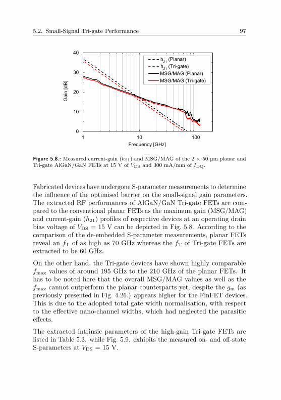
5.2. Small-Signal Tri-gate Performance 97
Figure 5.8.: Measured current-gain (ℎ21) and MSG/MAG of the 2 × 50 µm planar andTri-gate AlGaN/GaN FETs at 15 V of 𝑉DS and 300 mA/mm of 𝐼DQ.
Fabricated devices have undergone S-parameter measurements to determinethe influence of the optimised barrier on the small-signal gain parameters.The extracted RF performances of AlGaN/GaN Tri-gate FETs are com-pared to the conventional planar FETs as the maximum gain (MSG/MAG)and current-gain (ℎ21) profiles of respective devices at an operating drainbias voltage of 𝑉DS = 15 V can be depicted in Fig. 5.8. According to thecomparison of the de-embedded S-parameter measurements, planar FETsreveal an 𝑓T of as high as 70 GHz whereas the 𝑓T of Tri-gate FETs areextracted to be 60 GHz.
On the other hand, the Tri-gate devices have shown highly comparable𝑓max values of around 195 GHz to the 210 GHz of the planar FETs. Ithas to be noted here that the overall MSG/MAG values as well as the𝑓max cannot outperform the planar counterparts yet, despite the 𝑔m (aspreviously presented in Fig. 4.26.) appears higher for the FinFET devices.This is due to the adopted total gate width normalisation, with respectto the effective nano-channel widths, which had neglected the parasiticeffects.
The extracted intrinsic parameters of the high-gain Tri-gate FETs arelisted in Table 5.3. while Fig. 5.9. exhibits the measured on- and off-stateS-parameters at 𝑉DS = 15 V.
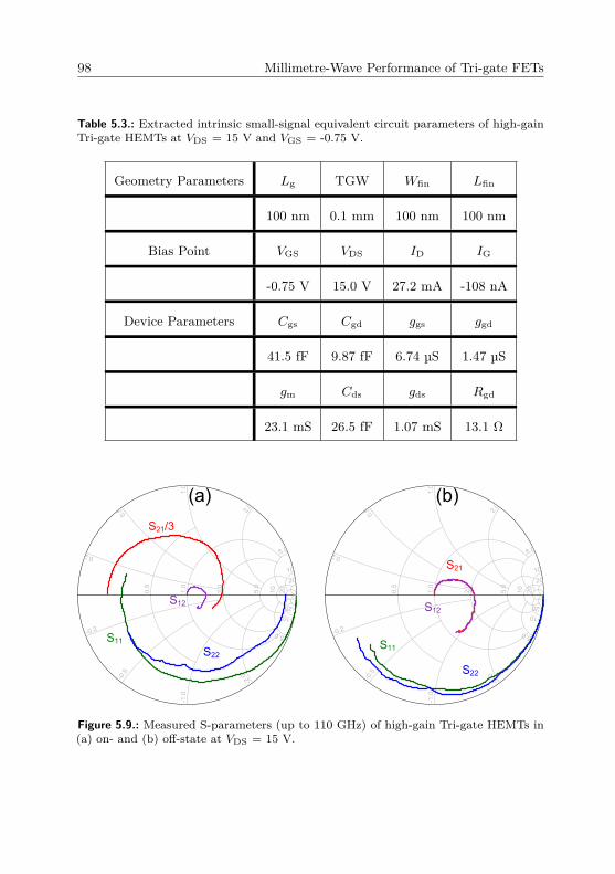
98 Millimetre-Wave Performance of Tri-gate FETs
Table 5.3.: Extracted intrinsic small-signal equivalent circuit parameters of high-gainTri-gate HEMTs at 𝑉DS = 15 V and 𝑉GS = -0.75 V.
Geometry Parameters 𝐿g TGW 𝑊fin 𝐿fin
100 nm 0.1 mm 100 nm 100 nm
Bias Point 𝑉GS 𝑉DS 𝐼D 𝐼G
-0.75 V 15.0 V 27.2 mA -108 nA
Device Parameters 𝐶gs 𝐶gd 𝑔gs 𝑔gd
41.5 fF 9.87 fF 6.74 µS 1.47 µS
𝑔m 𝐶ds 𝑔ds 𝑅gd
23.1 mS 26.5 fF 1.07 mS 13.1 Ω
Figure 5.9.: Measured S-parameters (up to 110 GHz) of high-gain Tri-gate HEMTs in(a) on- and (b) off-state at 𝑉DS = 15 V.

5.2. Small-Signal Tri-gate Performance 99
5.2.2. Investigation on the RF Linearity of Tri-gate
As much as the peak values of 𝑔m and small-signal gain parameters areessential figures of merit, their profiles with respect to the bias point areeven more critical from an application point of view. One of the majorproblems observed in short-channel devices in that respect is the non-linearity of performance. Fig. 5.10. depicts the typical behaviour of thedrain current and 𝑔m of the fabricated conventional planar AlGaN/GaNHEMTs.
Figure 5.10.: DC-transfer characteristic and the behaviour of the 𝑔m for planar HEMTswith the typical small- and large-signal swings indicated.
It can be noticed here that having reached its peak value, the 𝑔m beginsto drop quite severely as the 𝑉GS is increased. Such non-linearity of thetransconductance builds up adverse conditions while it is particularly unde-sired for the large-signal operation. The vertical line in Fig. 5.10. indicatesthe small-signal operation bias while the shaded region represents thetypical large-signal range of points, given the corresponding voltage swing.As a result, the effective value of 𝑔m under large-signal operation becomesa superposition of this entire range of points which causes the large-signalpower gain to appear lower than the small-signal gain. Overcoming thereduction in the large-signal gain can only be accomplished by preventingthe drop in the effective 𝑔m, thus, by making it flatter throughout allbias points. Due to the reduced gate capacitance only at high gate-source

100 Millimetre-Wave Performance of Tri-gate FETs
bias voltages and improved electrostatics with less bias dependence of 𝑔m,it makes the Tri-gate topology a perfect candidate for achieving higherlinearity in terms of cut-off frequency (i.e. 𝑓T).
Figure 5.11.: Extracted HF transconductances of (a) planar and (b) Tri-gate Al-GaN/GaN HEMTs as a function of 𝑉DS and 𝑉GS.
In an attempt to investigate the linearity of Tri-gate HEMTs, the first passof the developed FinFET structures (𝐿fin = 𝑊fin = 𝑊trench = 100 nmwith the 22-nm Al0.22Ga0.78N epitaxy variant) have undergone a detailed

5.2. Small-Signal Tri-gate Performance 101
bias-dependent characterisation and modelling. By performing series of S-parameter measurements throughout a vast range of bias points, (between-4 V and +3 V of 𝑉GS while up to 15 V of 𝑉DS) the parameters of the8-element small-signal equivalent circuit have been extracted for each biaspoint with the help of 3-D FET models. Fig. 5.11. exhibits the behaviourof the dynamic 𝑔m over 𝑉GS and 𝑉DS calculated for planar and Tri-gateFETs by applying (5.6). The maximum value achieved in the planar FETappears as high as 300 mS/mm which gets reduced to 270 mS/mm at𝑉DS = 15 V in combination with a strong 𝑉GS dependence. On the otherhand, the Tri-gate FET can reach up to 250 mS/mm which is sustainedover the entire 𝑉DS range. Its dependence on the gate bias voltage is alsoconsiderably lower as opposed to the planar FET.
Moving on to the influence on the HF performance, the comparison of the𝑓T responses can be seen in Fig. 5.12. As the results certify, the planar-gatedevices point out that as high as 75 GHz of 𝑓T is achieved at the operationbias point of 𝑉DS = 15 V and 𝑉GS = -1.9 V. As for the Tri-gate case, aflatter 𝑓T profile is maintained by the FinFETs over a large gate and drainbias range with a maximum value of 70 GHz at 𝑉DS = 15 V and 𝑉GS= -0.8 V. Accompanied by the flatter 𝑔m of Tri-gate devices, the 𝑓T wasable to be boosted and made more uniform. Once again, the reductionof SCE through implementation of the Tri-gate topology is proven sincethe frequency performance has become flatter throughout both the gatebias voltages (in agreement with Lee et al. [118]) as well as the drain biasvoltages. The influence of the SCE on the cut-off frequency can be bestdescribed by the following relation:
𝑓T = 𝑣e
2𝜋𝐿g,eff, (5.13)
in which 𝑣e denotes the effective electron velocity and 𝐿g,eff the effectivegate length. Reciprocally, the total time delay can be calculated as:
𝜏 = 1𝑓T
= 2𝜋(𝐿g,physical + 𝐿g,fringe)𝑣e
= 2𝜋(𝐶gs + 𝐶gd)𝑔m
, (5.14)
where 𝐿g,physical is the physical length of the gate while 𝐿g,fringe definesthe additional length including the fringing effects.

102 Millimetre-Wave Performance of Tri-gate FETs
Figure 5.12.: Extracted 𝑓T behaviour of (a) planar and (b) Tri-gate AlGaN/GaN HEMTsas a function of 𝑉DS and 𝑉GS.
Having demonstrated the promising 𝑔m and 𝑓T linearity of AlGaN/GaNFinFETs, further experiments have been carried out to improve the uni-formity by reducing the bias dependence. It has been discovered thatadopting the lattice-matched epitaxy variant with an In0.1Al0.55Ga0.35Nbarrier holds the key towards achieving a completely bias-independent 𝑓Tperformance. The investigation of the DC parameters in Chapter 4 haspointed out that SCE are suppressed by the implementation of Tri-gate

5.2. Small-Signal Tri-gate Performance 103
topology, hinting at the bias-independence of the performance. In additionto the DC performance analysis, small-signal investigation has also beenperformed which is followed by the extraction of intrinsic 𝑓T parameters.As demonstrated earlier, a non-linear behaviour is caused by the stronglybias-dependent nature of the dynamic 𝑔m, which has a negative impact onthe 𝑓T of the conventional planar-gate transistors.
Figure 5.13.: Extracted 𝑓T behaviour of (a) planar and (b) Tri-gate InAlGaN HEMTsas a function of 𝑉DS and 𝑉GS.

104 Millimetre-Wave Performance of Tri-gate FETs
The AlGaN/GaN FinFETs have already shown that a more linear 𝑓Tresponse can be achieved throughout higher gate and drain bias voltages.This effect is proven to be even more predominant in InAlGaN FinFETs asseen in the following results. The intrinsic 𝑓T profiles extracted from the S-parameter measurements of the planar FETs are exhibited in Fig. 5.13. (a).Accordingly, the peak value of 90 GHz is reached at a bias point of 𝑉GS= -4 V, 𝑉DS = 15 V. As soon as the drain bias is changed to either 𝑉DS= 20 V or 10 V, an immediate drop down in the 𝑓T can be observed. Iteven drops down to around 40 GHz once the gate bias voltage is increasedin combination with the drain bias voltage. However, it can be seen inFig. 5.13. (b) that the InAlGaN FinFETs have proven an almost bias-independent behaviour, remaining above 60 GHz and showing a peak upto 70 GHz, which is an advantageous feature for high-gain power amplifierapplications.
5.3. Large-Signal Tri-gate Performance
In the previous Section the development of Tri-gate devices with enhancedsmall-signal performance has been presented. Aiming for the main mo-tivation point of this work, Tri-gate GaN HEMTs have been developedfor power amplifier applications by profiting from the outcome of bothDC and small-signal analyses. Since high output power MMW FETs arerequired for the intended application, the large-signal performance of thedevices needs to be investigated and subsequently optimised.
The accomplishments, that have been put forward during the small-signalinvestigation, allow for an enhanced large-signal behaviour for GaN Tri-gate HEMTs. In the light of all the information gathered until this point,a thorough analysis and optimisation of the large-signal figures of meritwill be presented in this Section. In order to achieve superior large-signalperformance, the critical parameters responsible for the output powerdensity of HF transistors must be improved such as the drain currentdensity and the operation drain bias point.
With the help of the above-mentioned achievements regarding small-signalgain, cut-off frequency, and saturation drain current density of the devel-oped Tri-gate GaN HEMTs, high-performance MMW FETs can finally be

5.3. Large-Signal Tri-gate Performance 105
realised with considerably higher output power density. The RF outputpower of a transistor is primarily dependent on two base parameters,namely, the maximum output voltage swing and the maximum outputcurrent (in other words the saturation drain current density). Suppres-sion of the SCE in Tri-gate FETs allows for the reduction of the drainvoltage dependence of the intrinsic device parameters thus, increasing theeffective output voltage range. Furthermore, adoption of the advancedheterostructures facilitates exploiting the current capability of FinFETswhich reaches close to the limits of the GaN material properties.
Due to its critical advantages in terms of enriched 2DEG density andvery low sheet resistance, the epitaxy variant with an AlN barrier hasbeen selected for the development of high-power Tri-gate FETs. Initially a4-nm-thick AlN has been utilised which will then be varied to determinethe influence of the barrier thickness on the large-signal performance ofTri-gate FETs. Together with the barrier thickness, the ohm contactshave also been optimised to minimise the 𝑅cont as already depicted inFig. 4.32. It can be manifested that the quality of contacts significantlyaffects the large-signal gain and output power of the developed MMWFETs.
Figure 5.14.: Measured ℎ21 and MSG/MAG of the initial 2 × 50 µm planar and Tri-gateAlN/GaN FETs at 𝑉DS = 15 V.

106 Millimetre-Wave Performance of Tri-gate FETs
Before investigating the large-signal behaviour of AlN/GaN devices, asmall-signal characterisation is needed to compare the gain and cut-offfrequency of planar and Tri-gate HEMTs. Fig. 5.14. sets display tothe measured MSG/MAG responses of the initial (with poor contacts)planar and Tri-gate AlN/GaN HEMTs as a function of frequency. At atypical operating drain bias voltage of 𝑉DS = 15 V, the 𝑓max of FinFETsis extrapolated to appear around 140 GHz whereas an 𝑓T of 60 GHz isdetermined according to the ℎ21 extraction. The absolute values of cut-offfrequencies appear slightly lower than of the respective devices with anAlGaN barrier as a result of a high 𝑅cont with the unoptimised contactforming process. The slight decrease in the Tri-gate k-point can also beassociated to the marginal increase in the 𝑅g. But more importantly,Tri-gate FETs have unmistakably outperformed the planar counterpartswith increased gain and approximately 10 GHz higher 𝑓T.
Concerning the high-power operation, large-signal performances havefinally been determined through load-pull (LP) measurements at 30 GHzof frequency, 15 V of 𝑉DS, and class-A biasing (𝐼DQ = 0.5 A/mm) whichhave shown output power densities up to 2.5 W/mm (by using traditionalgate-width normalisation for both devices) with 35% of drain efficiency asseen in Fig. 5.15.
Figure 5.15.: Measured large-signal performance of the initial planar and Tri-gateAlN/GaN FETs at 30 GHz and 𝑉DS = 15 V (normalised to the metallurgical gatewidth).

5.3. Large-Signal Tri-gate Performance 107
The difference in performances of the planar and Tri-gate devices ismarginal since an equal drain bias has been applied to both transistorsalthough, the prime advantage of the Tri-gate FETs is anticipated to bethe ability to sustain its gain and efficiency performance at high 𝑉DS whiledelivering higher output power owing to less bias dependence. However,higher drain bias voltages could not be applied to the initial set of AlNdevices due to measurement limitations in terms of load impedances. Ac-counting for 2×50 µm FETs, the real part of the optimum load impedancethat needs to be presented to the output of the transistor exceeds 500 Ωwhich is the effective limit of the passive load tuner in the LP measure-ment setup. Larger transistors with higher TGW are therefore needed toenable such LP measurements which are then realised within the optimisedAlN/GaN Tri-gate process.
As for the optimisation of the AlN/GaN Tri-gate devices towards large-signal performance, the epitaxy has been varied by means of playingwith the barrier thickness. The electrical properties achieved on waferswith respective AlN thickness have been listed in Table 5.4. Accordingto the results the highest 𝑛s of 2 × 1013 cm−2 has been obtained in the6.4-nm variant, with the slight reduction in the mobility. Together withthe optimised barrier, the ohm contact process has been improved byemploying Si-implantation as the results have already been presented inFig. 4.32. The measured 𝑅sheet after the contact formation step appearsat 348 Ω/sq for this variant.
Table 5.4.: Electrical parameters of the AlN/GaN wafers with varied barrier thickness.
Barrier/Parameter 4.3-nm AlN 6.4-nm AlN 8.2-nm AlN
𝜇0
[cm2/Vs] 1420 854 876𝑛𝑠
[cm−2] 1.2 × 10¹³ 2.0 × 10¹³ 1.9 × 10¹³
𝑅sheet[Ω/sq] 375 348 377

108 Millimetre-Wave Performance of Tri-gate FETs
Having optimised the epitaxy and the ohm contacts of AlN/GaN process,a new set of Tri-gate FETs have been designed and fabricated with aTGW of 2 × 150 µm = 300 µm. The increased width of the gate fingersenables the reduction of the optimum load impedance well below 500 Ωthus, making it suitable for LP measurements at higher 𝑉DS. The influenceof the optimisation of the epitaxy and the ohm contact process can also bedistinguished in the small-signal behaviour of the AlN/GaN Tri-gate FETs.Fig. 5.16. illustrates the intrinsic 𝑓T profile of the optimised devices whichresulted in a peak value of 80 GHz, certifying a significant improvementover the 60 GHz of the first-pass design. Once again, the flatness of 𝑓Twith respect to the bias points agrees with the anticipated and desiredbehaviour as 50 GHz can still be maintained over the complete bias rangeas long as the device is switched on and the bias is kept above the kneevoltage.
Figure 5.16.: Extracted 𝑓T behaviour of the optimised Tri-gate AlN/GaN FETs as afunction of 𝑉DS and 𝑉GS.

5.3. Large-Signal Tri-gate Performance 109
In order to reveal the large-signal performance of optimised AlN/GaNTri-gate devices, LP measurements have been performed once again at30 GHz. Concerning the bias point, a class-AB point have been selectedwith 𝐼DQ = 300 mA/mm while the drain bias point have been increased to20 V in this case. The power sweep taken at the optimum load impedancepoint is depicted in Fig. 5.17.
Figure 5.17.: Measured large-signal power sweep of the optimised Tri-gate AlN/GaNFET at 𝑉DS = 20 V and 𝑓 = 30 GHz.
According to the measurements, a saturated output power of 30.8 dBm(1.2 W) has been recorded while reaching a maximum drain efficiency ofmore than 30%. The linear power gain is measured to be around 9 dB,descending down to 5 dB in compression. In the light of the achieved resultsit can be concluded that with more than 1 W of continuous wave (CW)RF output power, a single multi-finger Tri-gate FET with an improvedAlN barrier is well-suited to be used as a main building block in MMWpower amplifier designs.
Regarding the overall results of the LP measurements, a comparisonbetween the initial planar and the optimised Tri-gate FETs can be seen inFig. 5.18. where it can be acknowledged that the output power density havesuccessfully been boosted up to 3.7 W/mm with 33% of drain efficiency asa result of the established operation at 𝑉DS = 20 V.

110 Millimetre-Wave Performance of Tri-gate FETs
Figure 5.18.: Measured large-signal performance of the initial planar FETs (𝑉DS =15 V) and optimised Tri-gate AlN/GaN FETs (𝑉DS = 20 V) at 30 GHz (normalised tothe metallurgical gate width).
5.4. Chapter Conclusion
In this Chapter, the successful MMW operation as well as a thoroughHF characterisation of the designed Tri-gate FETs were demonstrated.The investigation of the gate parasitics were addressed which indicatedthe influence of the Tri-gate design on cut-off frequencies. It was thenmade possible to reduce the parasitic and the on-state gate capacitance bymeans of fin optimisation. The detailed small-signal investigation showedthat not only high-gain Tri-gate HEMTs were able to be achieved, but alsoa more linear performance with significantly flatter 𝑓T responses. Suchbias-independence of the small-signal performance, in combination withthe improved saturation drain current density of the Tri-gate devices,allowed for achieving superior large-signal characteristics with increasedoutput power density through establishment of the high-𝑉DS operation.
Assisted by a more linear RF-𝑔m of the Tri-gate FETs, the reduction in the𝐶gs at high bias points and the minimised 𝑔ds promoted the establishmentof an almost bias-independent MMW performance, showing more than60 GHz of 𝑓T regardless of the bias voltages. The subsequent optimisationof the Tri-gate large-signal power performance, by employing AlN barrier

5.4. Chapter Conclusion 111
structures, led to a maximum output power density of 3.7 W/mm (witha simultaneous 𝑓T of 80 GHz) which is one of the highest values amongstate-of-the-art MMW GaN technologies. Following the determination offavourable RF-characteristics, circuit-level performances of the Tri-gatedevices are demonstrated in the next Chapter.


6. GaN Tri-gate DemonstratorCircuits
The establishment of a high-performance Tri-gate technology based onGaN HEMTs has been the main goal of this research. Accordingly, thedesign and fabrication procedure of the developed devices as well asthe optimisation of the most critical base performance parameters havebeen discussed in the previous Chapters. This Chapter will focus onthe demonstration of the developed GaN Tri-gate HEMT technology inregard to the use in both high-power MMW amplifier and high-speed logicapplications. For that purpose, several monolithic microwave integratedcircuit (MMIC) designs have been studied, including pre-matched multi-finger FETs, a linear power amplifier, and high-speed logic inverters, whoserespective performances have been analysed.
6.1. Millimetre-Wave Power Amplifiers
Development of high-performance FETs suitable for using in power am-plifier (PA) applications in MMW frequencies has been one of the majormotivation points of this work. On that account, scaling the size of anindividual active HEMT element is an integral part of the progress towardsmaximising the RF output power of a complete PA circuit. It is thereforeimperative to optimise the transistor layout by means of employing multi-ple gate fingers in order to be able to design highly-scaled devices withenhanced large-signal power performance to reach this goal. The assessingof pre-matched FETs and the design of a MMW GaN Tri-gate PA will bepresented in this Section.

114 GaN Tri-gate Demonstrator Circuits
6.1.1. Pre-Matched High-Power Tri-gate FETs
As much as the initial CPW FET design utilised until this point exhibitsthe mentioned benefits in terms of ease of fabrication and well-definedRF properties, its relatively low total gate width (TGW) strictly limitsthe delivered output power. Within the scope of this research, it is vitalto develop the Tri-gate technology to demonstrate Watt-level RF outputpower out of a single HEMT device at MMW frequencies. Even whenassuming 4 W/mm of output power density at the device level, the deliveredpower by using TGW = 100 µm FETs falls well behind of this target. Oncea more realistic power density of 3 – 3.5 W/mm is considered, it becomesapparent that the TGW must be increased to meet the demand.
The TGW scaling can be considered to constitute the first step of transitionfrom a device-level design into the circuit-level. While scaling the size ofthe transistor for higher RF output power, it is equally important not todepreciate the device characteristics nor exceed its thermal capabilities.One major concern of a highly-scaled gate width is the potential negativeinfluence on the small-signal parameters and performance. The widthof an individual gate finger at this point shows up to be one of thedetermining factors for the cut-off frequency. Resulting from the raisedeffective inductance and series resistance of the gate electrode, stretchingthe finger above 50 µm to increase the TGW will inevitably deteriorate the𝑓max and the overall MMW performance. Hence, an alternative approachhas to be followed by means of parallelising multiple gate fingers integratedin a single FET unit cell.
For a first-pass FET scaling through gate finger parallelisation, pre-matchedtransistors have been designed and fabricated to be able to evaluate thebase performance of the main building blocks of a PA circuit. In thisdesign, 4 gate fingers have been employed, exhibiting a TGW of 200 µm.Alongside with the active devices, passive components such as transmissionlines and MIM capacitors are used for the matching networks. A dedicatedinput matching network (IMN) provides the required input impedancetrajectory for an ideal power-matching between 10 – 30 GHz whereas abasic output matching (OMN) and combining network presents the loadimpedances with an acceptable mismatch level in a very broadband fashionup to 60 GHz.

6.1. Millimetre-Wave Power Amplifiers 115
Figure 6.1.: Chip photograph of the pre-matched 4 × 50 µm GaN Tri-gate FETs forlinear power amplifier design.
As for the fabrication, the half-process scheme which have been describedin Chapter 4 is adopted. In this case, only the first metal layer is utilisedduring the front-side processing for the prompt fabrication of the devices.A chip photograph of the pre-matched GaN FET is shown in Fig. 6.1. Inthe absence of the full-process elements such as air bridges, multiple metallayer stacks, and via holes, the interconnects between separate groundplanes of the two sets of gate fingers have been realised through the ohmcontact metal stack. Another function of the ohm metallisation layer isthe formation of an equivalent MIM capacitor, making use of the firstpassivation nitride layer between the first metal layer. However, in practice,the interconnects have presented a relatively high impedance instead ofan ideal short-circuit, due to either its raised inductance or resistance asa result of the thin layer. In the end, such a non-ideal definition of thecommon-ground have induced a low-pass filter effect, shifting the cut-offfrequencies of the circuit lower than the anticipated values. Nevertheless,the complete characterisation of the pre-matched devices indicate that it isstill functional at the lower end of the intended band of operation, where itcan provide useful information towards a complete PA design. The small-signal S-parameter measurement results of the fabricated pre-matchedTri-gate FETs are given in Fig. 6.2.

116 GaN Tri-gate Demonstrator Circuits
Figure 6.2.: Simulated (dashed curves) and measured (solid curves) S-parameters of thepre-matched GaN Tri-gate FETs at 𝑉DS = 15 V, 𝐼DQ = 300 mA/mm.
According to the obtained results the cut-off profile can immediately beobserved in the gain (𝑆21) curve above around 10 – 15 GHz where themeasured behaviour greatly deviates from the predicted values. Despitethis, an adequate matching has been achieved as the reflection coefficientsare in agreement with the simulations. Regarding the input matching,the two intended resonance points at 15 and 30 GHz have been met withapproximately -10 dB of 𝑆11. A reasonable output matching has also beengranted with measured 𝑆22 values of better than -5 dB over the entirefrequency range. On the other hand, the expected 8 – 9 dB of 𝑆21 couldnot be maintained up to 30 GHz but only until 15 GHz.
In spite of the cut-off frequency decrease, a large-signal investigation canstill be carried out at frequencies lower than the cut-off point, taking theadvantage of the broadband matching. In that regard, 10 GHz has beenchosen as the frequency of analysis at which the pre-matched Tri-gateFETs have undergone large-signal power measurements. Although, sincethe 4-finger FETs still require relatively high output impedances with anoutput return loss of around 5 dB, a 100 Ω of load impedance has beenpresented to the devices by the passive load tuner instead of the standard50 Ω environment. Fig. 6.3. exhibits the measured power sweep of thepre-matched FET at 𝑉DS = 30 V. More than 1 W (30 dBm) of CW output

6.1. Millimetre-Wave Power Amplifiers 117
power have been delivered with 35% of drain efficiency which correspondsto a record power density of 5 W/mm.
Figure 6.3.: Measured large-signal power sweep of the pre-matched GaN Tri-gate FETsat 𝑉DS = 30 V, 𝑓 = 10 GHz, and a presented output impedance of 100 Ω.
6.1.2. GaN Tri-gate MMW Power Amplifier MMIC
In order to exploit the high-power capabilities of Tri-gate GaN HEMTs atMMW frequencies, design of a first ever FinFET PA MMIC operating atW-band has been made which can be used in a wide range of applicationssuch as satellite communications and scanning RADARs. As for the thedesign specifications, the PA has been aimed to deliver a saturated CWoutput power of 30 dBm (1 W) within the frequency range of 86–94 GHz. Ithas already been shown that individual multi-finger transistors are capableof reaching Watt-level large-signal operation with the help of extendedrobust performance at high drain bias voltages. The parallelisation of thedeveloped Tri-gate FETs in the MMIC design is therefore expected tomeet the output power specification.
At the output of the four-stage design, 4 HEMTs with a periphery of 8×35 µm each has been adopted. The driver stages are composed of 2× 8×30 µm and 8× 30 µm transistors which provide sufficient gain to drive thelarger FETs at the output stage. Fig. 6.4. exhibits the circuit schematic

118 GaN Tri-gate Demonstrator Circuits
of the designed PA which illustrates the input matching network (IMN),output matching network (OMN), and the inter-stage matching network(ISMN), alongside with the associated bias networks and the remainingpassive elements that have been employed.
Figure 6.4.: Schematic diagram of the four-stage GaN Tri-gate MMW PA design.
Regarding the design, the scalable large-signal FET models of the Tri-gatedevices are generated through modifying the existing planar FET modelsby means of embedding the difference in parasitic capacitance values.Load-pull simulations are then performed to determine the optimum loadimpedances. The chip photograph of the fabricated PA MMIC (occupyinga total area of 4.125 mm2) is shown in Fig. 6.5.
Figure 6.5.: Chip photograph of the realised GaN Tri-gate PA MMIC (dimensions:2.75 mm × 1.5 mm).

6.1. Millimetre-Wave Power Amplifiers 119
The on-wafer small-signal S-parameter measurements have been carried outto evaluate the performance of the designed PA. Each stage has been biasedat class-AB point with a quiescent current density of 𝐼DQ = 300 mA/mmwhich enables a trade-off between gain, linearity, and efficiency. The drainsupply voltage is set to 𝑉DS = 10 V. Fig. 6.6. presents the measured (solidcurves) and simulated (dashed curves) S-parameters of the PA MMIC. Areasonable fit between the simulated and measured small-signal gain (𝑆21)is obtained, however, a slight down-shift in the frequency response can benoticed in the results. Despite this, more than 15 dB of small-signal gainhas been established in the target frequency while the reflection coefficientsreveal an acceptable broadband input and output matching.
Figure 6.6.: Measured (solid curves) and simulated (dashed curves) S-parameters of theGaN Tri-gate MMW PA design at 𝑉DS = 10 V, 𝐼DQ = 300 mA/mm.
Large-signal power measurements are followed to complete the characteri-sation of the Tri-gate PA. The on-wafer measurement setup comprises aW-band driver amplifier and a Keysight E4419B power sensor alongsidewith attenuators and couplers which have been de-embedded up to 90 GHz.In terms of measurement conditions, the drain bias voltage is increasedto 15 V while the 𝐼DQ is kept at 300 mA/mm, trading off efficiency forhigher output power. The measured large-signal power sweep at 89 GHzwith, compared to the simulations can be examined in Fig. 6.7.

120 GaN Tri-gate Demonstrator Circuits
Figure 6.7.: Measured (solid curves) and simulated (dashed curves) large-signal powersweep of the Tri-gate PA MMIC at 89 GHz, 𝑉DS = 15 V, 𝐼DQ = 300 mA/mm.
The differences in the simulated and measured output power profiles canbe attributed to the previously-mentioned slight shift in the frequencyresponse and the uncertainty of the predicted FinFET load targets at thosefrequencies. Nevertheless, the measurements taken at 89 GHz indicatethat a saturated CW output power of 30.4 dBm (1.1 W) has been achievedwith more than 12 dB of compressed power gain and 8% of PAE. Fig. 6.8.exhibits the frequency behaviour of the large signal power measurementstaken at an average 1.5 dB of gain compression per stage, compared tothe simulations. According to the results more than 29 dBm of outputpower and 12 dB of transducer power gain has been recorded between85–90 GHz with at least 6% of PAE.
Therefore, it can be stated that multi-Watt capabilities of GaN Tri-gatedevices have been demonstrated with a basic, low-profile power amplifierdesign which points out the potential of higher MMW output power levelsin excess of 1 W by using more complex designs with higher levels ofFET parallelisation. On the other hand, it has been determined that aFinFET MMIC design at MMW frequencies tends to be very sensitive toslight changes in the input and output capacitances thus, a more accuratemodelling procedure for the FinFETs has to be carried out by employingfield-simulated scalable multi-finger models.

6.2. Integrated Mixed-Signal Circuits 121
Figure 6.8.: Measured (solid curves) and simulated (dashed curves) large-signal perfor-mance of the Tri-gate PA MMIC vs. frequency at 𝑉DS = 15 V, 𝐼DQ = 300 mA/mm,and 1.5 dB of gain compression per stage.
6.2. Integrated Mixed-Signal Circuits
6.2.1. High-Speed Direct Coupled FET Logics
Besides the appeal in MMW power amplifier applications, GaN Tri-gatetransistors exhibit equally promising features for use in very high-speedswitching and logic application fields. Recent studies have already demon-strated the potential of GaN FinFETs for switches [119,120] in combinationwith novel super-lattice heterostructures [121, 122]. As the demand forhigh-speed operation keeps increasing with tens of gigabits per second ofrequired bitrates, particularly in the optical communications, employmentof direct-coupled FET logic (DCFL) devices has gained more attentionwhich provide high levels of integration and switching speed. Since theDCFL circuits typically comprise E-mode FETs as driver and D-mode asload transistors, difficulties in the fabrication process can be encounteredin which E/D integration is needed. At this point the use of GaN Tri-gate devices brings great advantages which permits ease of monolithicallyintegrated fabrication of E- and D-mode FETs on the same chip.

122 GaN Tri-gate Demonstrator Circuits
One of the basic components of a DCFL circuitry is considered to bean E/D inverter. Fig. 6.9. illustrates the schematic and the operationprinciple of a DCFL E/D inverter which converts the logic low (0 V) appliedat the input of the device to the logic high (positive supply voltage i.e.+𝑉DD) and vice versa. An E-mode FET is therefore required at the inputwhile a complementary D-mode FET is utilised in cascode configuration.Thereupon, digital FETs and circuits in DCFL configuration have beendesigned and realised which will assist evaluating the feasibility of Tri-gateGaN HEMTs in high-speed logics.
Figure 6.9.: Schematic diagram and illustration of the DCFL E/D mode inverter design.
6.2.2. Integrated E/D Mode Cascode Inverter
In order to demonstrate the suitability of the developed E- and D-modeGaN Tri-gate HEMT technology to the high-speed logics, a cascode inverterin DCFL topology has been designed and the on-wafer characterisationof the fabricated circuit has been carried out. The Tri-gate E-mode FEThas been cascoded with a D-mode planar FET by taking advantage of theability to co-fabricate both devices without undergoing complex processschemes such as localised channel doping or gate recess. In this first passdesign, both FETs in the cascode setup has been dimensioned to exhibitthe same TGW of 100 µm. Fig. 6.10. exhibits the layout of the fabricatedE/D mode cascode inverter.
Another advantage of the GaN Tri-gate DCFL can be distinguished in theform of its capability to operate at high operating voltages which translatesinto an increased inverter gain. The base characterisation of the invertercircuit has been performed by determining the transfer behaviour at variedhigh-state voltages up to 15 V. The resulting transfer characteristics

6.2. Integrated Mixed-Signal Circuits 123
Figure 6.10.: Chip photograph of the fabricated DCFL GaN Tri-gate E/D mode cascodeinverter.
measured at 𝑉DD = 1 V, 5 V, and 15 V are given in Fig. 6.11. It can benoticed that the logic 0 has been achieved with low-state voltages of 0.2 V,0.5 V, and 0.8 V at 1 V, 5 V, and 15 V of 𝑉DD, respectively. Considerableoffset currents flowing through the D-mode HEMT due to saturation draincurrent density imbalance between the E-mode FinFET prevents reachinglower output voltages, however, can easily be overcome by accordinglyre-dimensioning the TGW of the FETs.
Figure 6.11.: Measured transfer characteristics of the DCFL GaN Tri-gate E/D modecascode inverter at 𝑉DD = 1 V, 5 V, and 15 V.

124 GaN Tri-gate Demonstrator Circuits
The measured S-parameters of the DCFL inverter are given in Fig. 6.12.The results confirm a successful switching operation up to around 35–40 GHz with up to 8 dB of converter gain and more than 20 dB of isolation.The corresponding total delay is then extracted to be 25 ps.
Figure 6.12.: Measured S-parameters of the DCFL GaN Tri-gate E/D mode cascodeinverter at 𝑉DD = 5 V.
6.3. Chapter Conclusion
The demonstration of the circuit-level performance of the established GaNTri-gate HEMTs was presented in this Chapter. Aiming for the MMWPA applications, pre-matched multi-finger Tri-gate FETs were designed,capable of delivering Watt-level RF output power. A MMW Tri-gatepower amplifier MMIC for the first time demonstrated 30.4 dBm (1.1 W)of output power with 12 dB of transducer power gain and 8% of PAE at89 GHz. The straightforward monolithic integration of D- and E-modeFinFETs allowed for the design of DCFL circuits and a cascode inverter wasproposed which exhibited promising performance up to 40 GHz. In the end,it was determined that the GaN Tri-gate technology was suitable for MMWpower amplification and high-speed logics, making them viable candidatesfor mixed signal applications. The following Chapter summarises all ofthe achievements and assertions enabled by this research.

7. Conclusion and Outlook
7.1. Summary and Conclusion
The expanding data transfer rates in satellite communications, radiodetection and ranging (RADAR) applications, as well as various wirelesscommunication links have evoked the necessity of higher radio frequency(RF) output power levels to be delivered by the dedicated power amplifier(PA) components in such systems. Attaining sufficiently high solid-statepower at the millimetre-wave (MMW) frequencies, comparable to thatof the vacuum tube amplifiers, holds critical importance in achieving areliable and cost-effective operation in those applications. Owing to theexcellent material properties that GaN offers, a significant high-powerpotential has already been shown by GaN-based high electron mobilitytransistors (HEMTs). However, the lack of competitive GaN technologiesat and above the MMW frequencies has resulted in the dominance ofeither low-power solid-state devices based on GaAs and InP, or high-powervacuum tube amplifiers which are inefficient and impractical. In accordancewith that, the main focus of this thesis was based on the developmentof an improved GaN technology with superior performance by means ofcombining the Tri-gate device topology with the established MMW GaNHEMT technology.
As for the starting point, a rigorous optimisation procedure was carriedout to establish an applicable process scheme for the fabrication of GaNTri-gate devices which was slightly more complex than of the conventional,planar-gate transistors. In order to pattern high-quality 3-dimensionalnano-channel structures with critical dimensions in the sub-micron range,an electron-beam-defined mesa etching approach was taken for which theprocess parameters such as the etch depth and the trench geometry were

126 Conclusion and Outlook
optimised, enabling a satisfactory base performance with improved DC-characteristics. It was further evinced that an appropriate 3-D passivationand lateral dimensioning of the Tri-gate structures played elemental roles inmaximising the saturation drain current densities 𝐼D,sat and transconduc-tance 𝑔m, as well as in shifting the threshold voltage 𝑉th into the positivedirection which is preferred for the normally-off operation. As a decisiveoutcome of the optimisation progress, enhancement mode (E-mode) GaNFinFETs with normally-off behaviour (𝑉th = +0.2 V) were successfullydemonstrated.
Furthermore, a detailed investigation on the short channel effects (SCE)revealed the influence of the epitaxial layer composition on both on- andoff-state performances of the proposed Tri-gate HEMTs. Having minimisedthe SCE with the help of an enhanced gate control, outstanding on/offdrive current ratios as high as 108 were reached by using AlGaN/GaNheterostructures. On the other hand, the employment of a lattice-matchedInAlGaN barrier layer was proven to sharply reduce the drain bias depen-dence of the DC-and RF-parameters which was one of the most seriousdrawbacks of conventional GaN HEMTs. Conclusively, a pure AlN barrierwas finally adopted, resulting in an excellent DC performance with 𝐼D,satof 3.8 A/mm and a peak 𝑔m of 550 mS/mm.
Concerning the MMW performance of the designed Tri-gate devices, adetailed small-signal analysis and 3-D FET modelling indicated that boththe gate-source capacitance and dynamic output conductance were able tobe decreased. Such reductions of the parasitics allowed for significantlyflatter current-gain cut-off frequencies (𝑓T) with respect to the bias point.Up to 20 V of drain and +3 V of gate bias voltages, a highly-linear 𝑓T inexcess of 60 GHz was reached by the Tri-gate HEMTs with an InAlGaNbarrier. On the other hand, the combination of an AlN barrier withthe Tri-gate topology was determined to produce the highest RF outputpower density. Load-pull measurements taken at 30 GHz of fundamentalfrequency and 20 V of drain bias voltage resulted in a saturation outputpower density of as high as 3.7 W/mm. The results confirmed the benefitsof the elevated operation drain bias voltage, compared to the planar GaNFETs which were only able to deliver around 2.5 W/mm at 15 V of bias.In addition to this, an 𝑓T of 80 GHz was extracted at the given operationpoint which was also superior to that of the planar devices.

7.1. Summary and Conclusion 127
Finally, as a proof of concept, MMW power amplifier (PA) and cascodedlogic monolithic microwave integrated circuits (MMICs) utilising the GaNTri-gate FETs were designed. At the centre frequency of 89 GHz, thefirst ever FinFET PA MMIC delivered Watt-level saturated output power.Supported by the measured performance of the circuits, the feasibility ofboth D- and E-mode GaN FinFETs for MMW power amplifier, high-speedlogic and mixed signal applications was able to be demonstrated. Table 7.1.summarises the achieved figure of merits by the developed GaN-basedTri-gate devices together with those of the planar HEMTs.
Table 7.1.: Essential parameters of the GaN-based Tri-gate devices compared to theconventional GaN HEMTs (normalised to the metallurgical gate width).
Device Technology/Measured Parameter Planar GaN HEMT Tri-gate GaN HEMT
Max. drain current 1.5 A/mm 1.9 A/mm
Max. operation 𝑉DS <15 V 20 V
𝑔m linearity (Δ𝑉GS
with 0.8 × 𝑔m,peak )limited voltage swing
up to 𝑉th + 1.5 Vhigh voltage swingup to 𝑉th + 4 V
𝑓T linearity (Δ𝑉GS
with 0.8 × 𝑓T,peak )limited voltage swing
up to 𝑉th + 2 Vhigh voltage swingup to 𝑉th + 6 V
MMW power density 2.5 W/mm 3.7 W/mm
Thermal resistanceat 𝑃DC = 1 W 51 K/W 43 K/W
Peak 𝐶gs 0.54 pF/mm 0.66 pF/mm
Peak 𝑓T 100 GHz 80 GHz
RF parasitics identical identical
Device operationDepletion (D-mode)
𝑉th ≤ -1.6 VE- and D-mode
𝑉th = -1.2 .. +0.2 V
128 Conclusion and Outlook
7.2. Outlook
Since this work serves as a principle guideline in assessing a successful GaNTri-gate technology, further analyses remain to be performed in terms ofsystem-level performance evaluation, reliability investigation, and epitaxyoptimisation. The linearity characterisation of the designed PA MMIChas to be first of all made, in order to complete the investigation on thecircuit-level Tri-gate performance. Another topic which is subject to futureresearch is the verification of the reliability of Tri-gate HEMTs. The influ-ence of the raised operation bias voltage on the degradation behaviour andthe mean life-time needs to be analysed. Moreover, alternative approachestowards the normally-off operation remain to be sought, in combinationwith the novel epitaxial layers. It is evident that the above-mentioned ex-periments will shed more light on the physical mechanisms that determinethe performance of 3-dimensional GaN transistors and provide valuableinformation and guidance in exploiting their potential.

References
[1] U. K. Mishra, L. Shen, T. Kazior, and Y.-F. Wu, “GaN-based RFpower devices and amplifiers,” Proc. IEEE, vol. 96, pp. 287–305,Feb. 2008.
[2] Y.-F. Wu, A. Saxler, M. Moore, R. P. Smith, S. Sheppard,P. M. Chavarkar, T. Wisleder, U. K. Mishra, and P. Parikh, “30-W/mm GaN HEMTs by field plate optimization,” IEEE ElectronDevice Letters, vol. 25, no. 3, pp. 117–119, Mar. 2004.
[3] N. Sarazin, E. Morvan, M. A. di Forte Poisson, M. Oualli,C. Gaquiere, O. Jardel, O. Drisse, M. Tordjman, M. Magis, andS. L. Delage, “AlInN/AlN/GaN HEMT technology on SiC with10-W/mm and 50% PAE at 10 GHz,” IEEE Electron Device Letters,vol. 31, no. 1, pp. 11–13, Jan. 2010.
[4] N. Ikeda, Y. Niiyama, H. Kambayashi, Y. Sato, T. Nomura, S. Kato,and S. Yoshida, “GaN power transistors on Si substrates for switchingapplications,” Proc. IEEE, vol. 98, no. 7, pp. 1151-1161, Jul. 2010.
[5] R. Chu, A. Corrion, M. Chen, R. Li, D. Wang, D. Zehnder, B. Hughes,and K. Boutros, “1200-V normally off GaN-on-Si field-effect transis-tors with low dynamic on-resistance,” IEEE Electron Device Letters,vol. 32, pp. 632–634, May 2011.
[6] Y.-F. Wu, J. Gritters, L. Shen, R. P. Smith, and B. Swenson, “kV-class GaN-on-Si HEMTs enabling 99% efficiency converter at 800 Vand 100 kHz,” IEEE Transactions on Power Electronics, vol. 29,no. 6, pp. 2634-2637, Jun. 2014.
[7] C. Y. Tsai, T. L. Wu, and A. Chin, “High-performance GaN MOS-FET with high-k LaAlO3/SiO2 gate dielectric,” IEEE ElectronDevice Letters, vol. 33, no. 1, pp. 35–37, Jan. 2012.

130 References
[8] T. Zimmermann, D. Deen, Y. Cao, J. Simon, P. Fay, D. Jena,and H. G. Xing, “AlN/GaN insulated-gate HEMTs with 2.3 A/mmoutput current and 480 mS/mm transconductance,” IEEE ElectronDevice Letters, vol. 29, no. 7, pp. 661–663, Jul. 2008.
[9] R. S. Pengelly, S. M. Wood, J. W. Milligan, S. T. Sheppard, andW. L. Pribble, “A review of GaN on SiC high electron-mobility powertransistors and MMICs,” IEEE Transactions on Microwave Theoryand Techniques, vol. 60, no. 6, pp. 1764–1783, Jun. 2012.
[10] C. Campbell, A. Balistreri, M. Kao, D. Dumka, and J. Hitt, “GaNTakes the Lead,” IEEE Microwave Magazine, vol. 13, pp. 44–53,Sep. 2012.
[11] J. Schellenberg, B. Kim, and T. Phan, “W-Band, broadband 2 WGaN MMIC,” International Microwave Symposium Digest, pp. 1–4,Jun. 2013.
[12] A. Brown, K. Brown, J. Chen, K. C. Hwang, N. Kolias, and R. Scott,“W-band GaN power amplifier MMICs,” International MicrowaveSymposium Digest, pp. 1–3, Jun. 2011.
[13] T. Palacios, A. Chakraborty, S. Rajan, C. Poblenz, S. Keller,S. P. DenBaars, J. S. Speck, and U. K. Mishra, “High-power Al-GaN/GaN HEMTs for Ka-band applications,” IEEE Electron DeviceLetters, vol. 26, no. 11, pp. 781–783, Nov. 2005.
[14] J. S. Moon, D. Wong, M. Hu, P. Hashimoto, M. Antcliffe, C. McGuire,M. Micovic, and P. Willadson, “55% PAE and high power Ka-band GaN HEMTs with linearized transconductance via n+ GaNsource contact ledge,” IEEE Electron Device Letters, vol. 29, no. 8,pp. 834–837, Aug. 2008.
[15] M. Micovic, A. Kurdoghlian, H. P. Moyer, P. Hashimoto, M. Hu,M. Antcliffe, P. J. Willadsen, W. S. Wong, R. Bowen, I. Milosavljevic,Y. Yoon, A. Schmitz, M. Wetzel, C. McGuire, B. Hughes, andD. H. Chow, “GaN MMIC PAs for E-band (71–95 GHz) radio,”Proc. IEEE Compound Semiconductor Integrated Circuit Symposium(CSICS), pp. 1–4, Oct. 2008.

References 131
[16] Y. Nakasha, S. Masuda, K. Makiyama, T. Ohki, M. Kanamura,N. Okamoto, T. Tajima, T. Seino, H. Shigematsu, K. Imanishi,T. Kikkawa, K. Joshin, and N. Hara, “E-Band 85-mW oscillator and1.3-W amplifier ICs using 0.12-um GaN HEMTs for millimeter-wavetransceivers,” Proc. Compound Semiconductor Integrated CircuitSymposium, pp. 1–4, Oct. 2010.
[17] A. Crespo, M. M. Bellot, K. D. Chabak, J. K. Gillespie, G. H. Jessen,V. Miller, M. Trejo, G. D. Via, D. E. Walker, B. W. Winningham,H. E. Smith, T. A. Cooper, X. Gao, and S. Guo, “High-power Ka-band performance of AlInN/GaN HEMT with 9.8-nm-thin barrier,”IEEE Electron Device Letters, vol. 31, no. 1, pp. 2–4, Jan. 2010.
[18] M. Micovic, A. Kurdoghlian, A. Margomenos, D. Brown, K. Shi-nohara, S. Burnham, I. Milosavljevic, R. Bowen, A. Williams,P. Hashimoto, R. Grabar, C. Butler, A. Schmitz, P. Willadsen,and D. H. Chow, “92-96 GHz GaN power amplifiers,” InternationalMicrowave Symposium Digest, pp. 1–3, Jun. 2012.
[19] A. Brown, K. Brown, J. Chen, D. Gritters, K. Hwang, E. Ko, N. Ko-lias, S. O’Connor, and M. Sotelo, “High power, high efficiency E-bandGaN amplifier MMICs,” IEEE Int’l. Conf. Wireless InformationTechnology Systems Dig., pp. 1–4, Nov. 2012.
[20] C. F. Campbell, Y. Liu, M.-Y. Kao, and S. Nayak, “High efficiencyKa-band Gallium Nitride power amplifier MMICs,” Proc. IEEE In-ternational Conference on Microwaves, Communications, Antennasand Electronics Systems (COMCAS), pp. 1–5, Oct. 2013.
[21] D. C. Dumka, T. M. Chou, F. Faili, D. Francis, and F. Ejeckam,“AlGaN/GaN HEMTs on diamond substrate with over 7 W/mmoutput power density at 10 GHz,” Electronics Letters, vol. 49, no. 20,pp. 1298–1299, Sep. 2013.
[22] A. Margomenos, A. Kurdoghlian, M. Micovic, K. Shinohara,D. F. Brown, A. L. Corrion, H. P. Moyer, S. Burnham, D. C. Regan,R. M. Grabar, C. McGuire, M. D. Wetzel, R. Bowen, P. S. Chen,H. Y Tai, A. Schmitz, H. Fung, A. Fung, and D. H. Chow, “GaN tech-nology for E, W and G-band applications,” Proc. IEEE CompoundSemiconductor Integrated Circuit Symposium (CSICS), pp. 1–4,Oct. 2014.

132 References
[23] E. Camargo, J. Schellenberg, L. Bui, and N. Estella, “Power GaAsMMICs for E-band communications applications,” InternationalMicrowave Symposium Digest, pp. 1–4, Jun. 2014.
[24] D. Xu, K. K. Chu, J. A. Diaz, M. Ashman, J. J. Komiak, L. M. Pleas-ant, C. Creamer, K. Nichols, K. H. G. Duh, P. M. Smith, P. C. Chao,L. Dong, and P. D. Ye, “0.1-um atomic layer deposition Al2O3 pas-sivated InAlN/GaN high electron-mobility transistors for E-Bandpower amplifiers,” IEEE Electron Device Letters, vol. 36, no. 5,pp. 442–444, May 2015.
[25] K. Tsukashima, A. Otsuka, M. Kubota, T. Tokumitsu, and S. Ogita,“An E-band 1 W-class PHEMT power amplifier MMIC,” Proc. Euro-pean Microwave Integrated Circuits Conference (EuMIC), pp. 9–12,Sep. 2015.
[26] A. Bessemoulin, J. Tarazi, M. Rodriguez, M. G. McCulloch,A. E. Parker, and S. J. Mahon, “Reduced-size E-band GaAs poweramplifier MMIC,” Proc. European Microwave Integrated CircuitsConference (EuMIC), pp. 25–28, Sep. 2015.
[27] Y. Niida, Y. Kamada, T. Ohki, S. Ozaki, K. Makiyama, Y. Minoura,N. Okamoto, M. Sato, K. Joshin, and K. Watanabe, “3.6 W/mmhigh power density W-band InAlGaN/GaN HEMT MMIC poweramplifier,” Proc. IEEE Topical Conf. Power Amp. for Wireless andRadio Appl. (PAWR), pp. 24–26, Jan. 2016.
[28] H.-C. Lin and G. M. Rebeiz, “A 70–80-GHz SiGe amplifier with peakoutput power of 27.3 dBm,” IEEE Trans. Microw. Theory Techn.,vol. 64, no. 6, pp. 1–11, Jul. 2016.
[29] D. Schwantuschke, B.-J. Godejohann, S. Breuer, P. Bruckner,M. Mikulla, R. Quay, and O. Ambacher, “Broadband E-band poweramplifier MMIC based on an AlGaN/GaN HEMT technology with30 dBm output power,” Proc. IEEE Compound Semiconductor Inte-grated Circuit Symposium (CSICS), pp. 1–4, Oct. 2016.
[30] H. Sun, A. R. Alt, H. Benedickter, E. Feltin, J.-F. Carlin,M. Gonschorek, N. Grandjean, and C. R. Bolognesi, “205-GHz(Al,In)N/GaN HEMTs,” IEEE Electron Device Letters, vol. 31, no. 9,pp. 957–959, Sep. 2010.

References 133
[31] J. W. Chung, W. E. Hoke, E. M. Chumbes, and T. Palacios, “Al-GaN/GaN HEMT With 300-GHz fmax,” IEEE Electron DeviceLetters, vol. 31, no. 3, pp. 195–197, Mar. 2010.
[32] M. L. Schuette, A. Ketterson, B. Song, E. Beam, T.-M. Chou,M. Pilla, H.-Q. Tserng, X. Gao, S. Guo, P. J. Fay, H. G. Xing, andP. Saunier, “Gate-recessed integrated E/D GaN HEMT technologywith fT / fmax >300 GHz,” IEEE Electron Device Letters, vol. 34,no. 6, pp. 741–743, Jun. 2013.
[33] D. F. Brown, A. Williams, K. Shinohara, A. Kurdoghlian,I. Milosavljevic, P. Hashimoto, R. Grabar, S. Burnham, C. But-ler, P. Willadsen, and M. Micovic, “W-band power performance ofAlGaN/GaN DHFETs with regrown n+ GaN ohmic contacts byMBE,” Proc. IEEE International Electron Devices Meeting (IEDM),pp. 19.3.1–19.3.4, Dec. 2011.
[34] K. Shinohara, D. Regan, I. Milosavljevic, A. L. Corrion, D. F. Brown,S. Burnham, P. J. Willadsen, C. Butler, A. Schmitz, S. Kim, V. Lee,A. Ohoka, P. M. Asbeck, and M. Micovic, “Device scaling tech-nologies for ultra-high-speed GaN-HEMTs,” Proc. Device ResearchConference (DRC), pp. 275–278, Jun. 2011.
[35] K. Shinohara, D. Regan, A. Corrion, D. Brown, I. Alvarado-Rodriguez, M. Cunningham, C. Butler, A. Schmitz, S. Kim,B. Holden, D. Chang, A. Margomenos, M. Micovic, V. Lee, andP. M. Asbeck, “Deeply-scaled E/D-mode GaN-HEMTs for sub-mm-wave amplifiers and mixed-signal applications,” Proc. IEEE Compd.Semicond. Integrated Circuit Symp. (CSICS), pp. 1–4, Oct. 2012.
[36] K. Shinohara, D. Regan, A. Corrion, D. Brown, S. Burnham,P. J. Willadsen, I. Alvarado-Rodriguez, M. Cunningham, C. But-ler, A. Schmitz, S. Kim, B. Holden, D. Chang, V. Lee, A. Ohoka,P. M. Asbeck, and M. Micovic, “Deeply-scaled self-aligned-gateGaN DH-HEMTs with ultrahigh cutoff frequency,” Proc. IEEE In-ternational Electron Devices Meeting (IEDM), pp. 19.1.1–19.1.4,Dec. 2011.
[37] K. Shinohara, D. C. Regan, Y. Tang, A. L. Corrion, D. F. Brown,J. C. Wong, J. F. Robinson, H. H. Fung, A. Schmitz, T. C. Oh,

134 References
S. J. Kim, P. S. Chen, R. G. Nagele, A. D. Margomenos, and M. Mi-covic, “Scaling of GaN HEMTs and Schottky diodes for submillimeter-wave MMIC applications,” IEEE Transactions on Electron Devices,vol. 60, no. 10, pp. 2982–2996, Oct. 2013.
[38] Y. Tang, K. Shinohara, D. Regan, A. Corrion, D. Brown, J. Wong,A. Schmitz, H. Fung, S. Kim, and M. Micovic, “Ultrahigh-speedGaN high-electron-mobility transistors with fT / fmax of 454/444GHz,” IEEE Electron Device Letters, vol. 36, no. 6, pp. 549–551,Jun. 2015.
[39] B. S. Doyle, S. Datta, M. Doczy, S. Hareland, B. Jin, J. Kavalieros,T. Linton, A. Murthy, R. Rios, and R. Chau, “High performancefully-depleted tri-gate CMOS transistors,” IEEE Electron DeviceLetters, vol. 24, no. 4, pp. 263–265, Apr. 2003.
[40] D. Hisamoto, W.-C. Lee, J. Kedzierski, H. Takeuchi, K. Asano,C. Kuo, E. Anderson, T.-J. King, J. Bokor, and C. Hu, “FinFET-aself-aligned double-gate MOSFET scalable to 20 nm,” IEEE Transac-tions on Electron Devices, vol. 47, no. 12, pp. 2320–2325, Dec. 2000.
[41] T. Palacios, S. Rajan, A. Chakraborty, S. Heikman, S. Keller,S. P. DenBaars, and U. K. Mishra, “Influence of the dynamic accessresistance in the gm and fT linearity of AlGaN/GaN HEMTs,” IEEETrans. Electron Devices, vol. 52, no. 10, pp. 2117–2123, Oct. 2005.
[42] R. Kenny and J. Watt, “The breakthrough advantage for FPGAs withTri-Gate technology,” Altera & Intel Corp. White Paper, Sep. 2016.
[43] O. Ambacher, J. Smart, J. R. Shealy, N. Weimann, N. G. Chu,M. Murphy, W. Schaff, L. F. Eastman, R. Dimitrov, L. Wittmer,M Stutzmann, W. Rieger, and J. Hilsenbeck, “Two-dimensionalelectron gases induced by spontaneous and piezoelectric polarizationcharges in N- and Ga-face AlGaN/GaN heterostructures,” Journalof Applied Physics, vol. 85, no. 6, pp. 3222-3233, Mar. 1999.
[44] C. Skierbiszewski, K. Dybko, W. Knap, M. Siekacz, W. Krupczynski,G. Nowak, M. Bockowski, J. Lusakowski, Z. Wasilewski, D. Maude,T. Suski, and S. Porowski, “High mobility two-dimensional electrongas in AlGaN/GaN heterostructures grown on bulk GaN by plasma

References 135
assisted molecular beam epitaxy,” Applied Physics Letters, vol. 86,no. 10, pp. 102106-1–102106-3, Mar. 2005.
[45] M. N. Gurusinghe, S. K. Davidsson, and T. G. Andersson, “Two-dimensional electron mobility limitation mechanisms in AlGaN/GaNheterostructures,” Phys. Rev. B, vol. 72, no. 4, pp. 045316-1–045316-11, Jul. 2005.
[46] C. Haupt, S. Maroldt, R. Quay, W. Pletschen, A. Leuther, andO. Ambacher, “Development of a high transconductance GaN MMICtechnology for millimeter wave applications,” Physica Status Solidi,vol. 8, no. 2, pp. 297–299, Feb. 2011.
[47] O. Ambacher, B. Foutz, J. Smart, J. R. Shealy, N. G. Weimann,K. Chu, M. Murphy, A. J. Sierakowski, W. J. Schaff, L. F. Eastman,R. Dimitrov, A. Mitchell, and M. Stutzmann, “Two dimensionalelectron gases induced by spontaneous and piezoelectric polarizationin undoped and doped AlGaN/GaN heterostructures,” Journal ofApplied Physics, vol. 87, no. 1, pp. 334–344, Jan. 2000.
[48] K. Kohler, S. Muller, P. Waltereit, L. Kirste, H. P. Menner, W. Bron-ner, and R. Quay, “Growth and electrical properties of AlGaN/GaNheterostructures with different Al-content,” Physica Status Solidi,vol. 206, no. 11, pp. 2652–2657, Nov. 2009.
[49] Y. Liu, H. Jiang, S. Arulkumaran, T. Egawa, B. Zhang, andH. Ishikawa, “Demonstration of undoped quaternary AlInGaN/GaNheterostructure field-effect transistor on sapphire substrate,” Appl.Phy. Lett., vol. 86, no. 22, pp. 223510-1–223510-3, May 2005.
[50] Y. Liu, T. Egawa, and H. Jiang, “Enhancement-mode quaternaryAlInGaN/GaN HEMT with non-recessed-gate on sapphire substrate,”Electronics Letters, vol. 42, no. 15, pp. 884–886, Jul. 2006.
[51] R. Wang, G. Li, J. Verma, B. S. Rodriguez, T. Fang, J. Guo, Z. Hu,O. Laboutin, Y. Cao, W. Johnson, G. Snider, P. Fay, D. Jena,and H. G. Xing, “220-GHz quaternary barrier InAlGaN/AlN/GaNHEMTs,” IEEE Electron Device Letters, vol. 32, no. 9, pp. 1215–1217,Sep. 2011.

136 References
[52] T. Zimmermann, D. Deen, Y. Cao, J. Simon, P. Fay, D. Jena,and H. G. Xing, “AlN/GaN insulated-gate HEMTs with 2.3 A/mmoutput current and 480 mS/mm transconductance,” IEEE ElectronDevice Letters, vol. 29, no. 7, pp. 661–664, Jul. 2008.
[53] A. Bairamis, C. Zervos, A. Adikimenakis, A. Kostopoulos, M. Kayam-baki, K. Tsagaraki, G. Konstantinidis, and A. Georgakilas, “Electrondensity and currents of AlN/GaN high electron mobility transistorswith thin GaN/AlN buffer layer,” Appl. Phy. Lett., vol. 105, no. 11,pp. 113508-1–113508-5, Sep. 2014.
[54] R. Vetury, N. Q. Zhang, S. Keller, and U. K. Mishra, “The impactof surface states on the DC and RF characteristics of AlGaN/GaNHFETs,” IEEE Transactions on Electron Devices, vol. 48, no. 3,pp. 560–566, Mar. 2001.
[55] P. Aaen, J. Pla, and J. Wood, Modeling and characterization of RFand microwave power FETs, Cambridge University Press, 2007.
[56] G. H. Jessen, R. C. Fitch, J. K. Gillespie, G. Via, A. Crespo, D. Lang-ley, D. J. Denninghoff, M. Trejo, and E. R. Heller, “Short-channel ef-fect limitations on high-frequency operation of AlGaN/GaN HEMTsfor T-Gate devices,” IEEE Transactions on Electron Devices, vol. 54,no. 10, pp. 2589–2597, Oct. 2007.
[57] B. Lu, E. Matioli, and T. Palacios, “Tri-gate normally-off GaN powerMISFET,” IEEE Electron Device Letters, vol. 33, no. 3, pp. 360–362,Mar. 2012.
[58] K.-S. Im, Y.-W. Jo, K.-W. Kim, D.-S. Kim, H.-S. Kang, C.-H. Won, R.-H. Kim, S.-M. Jeon, D.-H. Son, Y.-M. Kwon, J.-H. Lee, S. Cristoloveanu, and J.-H. Lee, “First demonstration ofheterojunction-free GaN nanochannel FinFETs,” Proc. Int’l. Symp.Power Semicond. Devices and ICs, pp. 415–418, May 2013.
[59] S. Lee, J. Lee, and S. Cho, “Design and characterization of electricallyself-isolated GaN-on-Si junctionless fin-shaped channel field-effecttransistor with higher cost-effectiveness for low-power applications,”Jpn. J. Appl. Phys. vol. 54, no. 8, pp. 084301-1–084301-6, Jul. 2015.

References 137
[60] C.-Y. Chen and Y.-R. Wu, “Studying the short channel effect in thescaling of the AlGaN/GaN nanowire transistors,” Journal of AppliedPhysics, vol. 113, no. 21, pp. 214501-1-214501-8, Jun. 2013.
[61] R. Wang, Y. Cai, C.-W. Tang, K. Lau, and K. Chen, “Enhancement-mode Si3N4/AlGaN/GaN MISHFETs,” IEEE Electron Device Let-ters, vol. 27, no. 10, pp. 793–795, Oct. 2006.
[62] Z. H. Feng, R. Zhou, S. Y. Xie, J. Y. Yin, J. X. Fang, B. Liu, W. Zhou,K. J. Chen, and S. J. Cai, “18-GHz 3.65 W/mm enhancement-modeAlGaN/GaN HFET using fluorine plasma ion implantation,” IEEEElectron Device Letters, vol. 31, no. 12, pp. 1386–1388, Dec. 2010.
[63] X. Liu and K. J. Chen, “GaN single-polarity power supply boot-strapped comparator for high temperature electronics,” IEEE Elec-tron Device Letters, vol. 32, no. 1, pp. 27–29, Jan. 2011.
[64] K. Ohi and T. Hashizume, “Drain current stability and controllabil-ity of threshold voltage and subthreshold current in a Multi-mesa-channel AlGaN/GaN high electron mobility transistor,” Jpn. J. Appl.Phys., vol. 48, no. 8, pp. 081002-1–081002-5, Aug. 2009.
[65] P.-C. Yeh, Y.-W. Lin, Y.-L. Huang, J.-H. Hung, B.-R. Lin, L. Yang,C.-H. Wu, T.-K. Wu, C.-H. Wu, and L.-H. Peng, “Threshold volt-age controlled by gate area and gate recess in inverted trapezoidaltrigate AlGaN/GaN MOS high-electron-mobility transistors withphotoenhanced chemical and plasma-enhanced atomic layer deposi-tion oxides,” Appl. Phys. Exp. vol. 8, no. 8, pp. 084101-1–084101-4,Aug. 2015.
[66] T. Oka and T. Nozawa, “AlGaN/GaN recessed MIS-Gate HFETwith high-threshold-voltage normally-off operation for power elec-tronics applications,” IEEE Electron Device Letters, vol. 29, no. 7,pp. 668–670, Jul. 2008.
[67] W. Saito, Y. Takada, M. Kuraguchi, K. Tsuda, and I. Omura,“Recessed-gate structure approach toward normally off high-voltageAlGaN/GaN HEMT for power electronics applications,” IEEE Trans-actions on Electron Devices, vol. 53, no. 2, pp. 356–362, Feb. 2006.

138 References
[68] Y. Cai, Y. G. Zhou, K. J. Chen, and K. M. Lau, “High-performanceenhancement-mode AlGaN/GaN HEMTs using fluoride-based plasmatreatment,” IEEE Electron Device Letters, vol. 26, no. 7, pp. 435–437,Jul. 2005.
[69] I. Hwang, J. Kim, H. S. Choi, H. Choi, J. Lee, K. Y. Kim, J.-B. Park,J. C. Lee, J. Ha, J. Oh, J. Shin, and U-I. Chung, “p-GaN GateHEMTs with tungsten gate metal for high threshold voltage andlow gate current,” IEEE Electron Device Letters, vol. 34, no. 2,pp. 202–204, Feb. 2013.
[70] M. Kanamura, T. Ohki, T. Kikkawa, K. Imanishi, T. Imada, A. Ya-mada, and N. Hara, “Enhancement-mode GaN MIS-HEMTs withn-GaN/i-AlN/n-GaN triple cap layer and high-k gate dielectrics,”IEEE Electron Device Letters, vol. 31, no. 3, pp. 189–191, Mar. 2010.
[71] K. Shinohara, D. Regan, I. Milosavljevic, A. L. Corrion, D. F. Brown,P. J. Willadsen, C. Butler, A. Schmitz, S. Kim, V. Lee, A. Ohoka,P. M. Asbeck, and M. Micovic, “Electron velocity enhancementin laterally scaled GaN DH-HEMTs with fT of 260 GHz,” IEEEElectron Device Letters, vol. 32, no. 8, pp. 1074–1076, Aug. 2011.
[72] K.-S. Im, R.-H. Kim, K.-W. Kim, D.-S. Kim, C. S. Lee,S. Cristoloveanu, and J. H. Lee, “Normally off single-nanoribbonAl2O3/GaN MISFET,” IEEE Electron Device Letters, vol. 34, no. 1,pp. 27–29, Jan. 2013.
[73] K.-S. Im, C.-H. Won, Y.-W. Jo, J.-H. Lee, M. Bawedin,S. Cristoloveanu, and J. H. Lee, “High-performance GaN-basednanochannel FinFETs with/without AlGaN/GaN heterostructure,”IEEE Trans. Electron Devices, vol. 60, no. 10, pp. 3012–3018,Oct. 2013.
[74] Y.-W. Jo, D.-H. Son, C.-H. Won, V. Sindhuri, J.-H. Kim, J. H. Seo,I. M. Kang, and J.-H. Lee, “Control of transconductance in highperformance AlGaN/GaN FinFETs,” Proc. IEEE Int’l. Conf. PowerElectronics and Drive Systems (PEDS), pp. 684–686, Jun. 2015.
[75] Y.-W. Jo, D.-H. Son, C.-H. Won, K.-S. Im, J. H. Seo, I. M. Kang, andJ.-H. Lee, “AlGaN/GaN FinFET with extremely broad transconduc-

References 139
tance by side-wall wet etch,” IEEE Electron Device Letters, vol. 36,no. 10, pp. 1008–1010, Oct. 2015.
[76] V. Sindhuri, D.-H. Son, D.-G. Lee, S. Sakong, Y.-H. Jeong, I.-T. Cho,J.-H. Lee, Y.-T. Kim, S. Cristoloveanu, Y. Bae, K.-S. Im, and J.-H. Lee, “1/f noise characteristics of AlGaN/GaN FinFETs with andwithout TMAH surface treatment,” Microelectronic Engineering,vol. 147, pp. 134–136, Nov. 2015.
[77] K.-S. Im, H.-S. Kang, J.-H. Lee, S.-J. Chang, S. Cristoloveanu,M. Bawedin, and J.-H. Lee, “Characteristics of GaN and AlGaN/GaNFinFETs,” Solid-State Electronics, vol. 97, pp. 66–75, Jul. 2014.
[78] K.-S. Im, D.-H. Son, H.-K. Ahn, S.-B. Bae, J.-K. Mun, E.-S. Nam,S. Cristoloveanu, and J.-H. Lee, “Performance improvement of nor-mally off AlGaN/GaN FinFETs with fully gate-covered nanochannel,”Solid-State Electronics, vol. 89, pp. 124–127, Nov. 2013.
[79] K.-S. Im, Y.-W. Jo, J.-H. Lee, S. Cristoloveanu, and J.-H. Lee,“Heterojunction-free GaN nanochannel FinFETs with high perfor-mance,” IEEE Electron Device Letters, vol. 34, no. 3, pp. 381–383,Mar. 2013.
[80] M. Azize and T. Palacios, “Top-down fabrication of AlGaN/GaNnanoribbons,” Appl. Phys. Lett., vol. 98, no. 4, pp. 042103-1–042103-3, Jan. 2011.
[81] T. Tamura, J. Kotani, S. Kasai, and T. Hashizume, “Nearly temper-ature independent saturation drain current in a multi-mesachannelAlGaN/GaN high electron mobility transistor,” Appl. Phys. Exp.,vol. 1, no. 2, pp. 023001-1–023001-3, Feb. 2008.
[82] J. Asubar, K. Ohi, K. Nishiguchi, and T. Hashizume, “Improvedcurrent stability in multi-mesa-channel AlGaN/GaN transistors,”Phys. Status Solidi C, vol. 11, no. 3-4, pp. 857–861, Apr. 2014.
[83] K. Ohi, J. T. Asubar, K. Nishiguchi, and T. Hashizume, “Currentstability in multi-mesa-channel AlGaN/GaN HEMTs,” IEEE Trans.Electron Devices, vol. 60, no. 10, pp. 2997–3004, Oct. 2013.

140 References
[84] E. J. Jones, M. Azize, M. J. Smith, T. Palacios, and S. Gradecak,“Correlating stress generation and sheet resistance in InAlN/GaNnanoribbon high electron mobility transistors,” Applied Physics Let-ters, vol. 101, no. 11, pp. 113101-1–113101-5, Sep. 2012.
[85] M. Azize, A. L. Hsu, O. I. Saadat, M. Smith, X. Gao, S. Guo,S. Gradecak, and T. Palacios, “High-electron-mobility transistorsbased on InAlN/GaN nanoribbons,” IEEE Electron Device Letters,vol. 32, no. 12, pp. 1680–1682, Dec. 2011.
[86] B. Lu, E. Matioli, and T. Palacios, “Low Leakage Normally-offTri-gate GaN MISFET,” Proc. International Symposium on PowerSemiconductor Devices and ICs, pp. 33–36, Jun. 2012.
[87] S. Liu, Y. Cai, G. Gu, J. Wang, C. Zeng, W. Shi, Z. Feng, H. Qin,Z. Cheng, C. Chen, and B. Zhang, “Enhancement-mode operationof nanochannel array (NCA) AlGaN/GaN HEMTs,” IEEE ElectronDevice Letters, vol. 33, no. 3, pp. 354–356, Mar. 2012.
[88] S. Liu, Y. Cai, R. Gong, J. Wang, C. Zeng, W. Shi, Z. Feng, J. Wang,J. Yin, C. P. Wen, H. Qin, and B. Zhang, “Threshold voltage depen-dence on channel width in nano-channel array AlGaN/GaN HEMTs,”Phys. Status Solidi C, vol. 9, no. 3-4, pp. 879–882, Mar. 2012.
[89] S.-H. Liu, Y. Cai, R.-M. Gong, J.-Y. Wang, C.-H. Zeng, W.-H. Shi,Z.-H. Feng, J.-J. Wang, J.-Y. Yin, P. W. Cheng, H. Qin, and B.-S. Zhang, “Enhancement-mode AlGaN/GaN high electron mobilitytransistors using a nano-channel array structure,” Chin. Phys. Lett.,vol. 28, no. 7, pp. 077202-1–077202-3, Jul. 2011.
[90] Y.-W. Jo, D.-H. Son, D.-G. Lee, C.-H. Won, J. H. Seo, I. M. Kang,and J.-H. Lee, “First demonstration of GaN-based vertical nanowireFET with top-down approach,” Proc. Device Research Conference(DRC), pp. 35–36, Jun. 2015.
[91] D.-H. Son, Y.-W. Jo, R.-H. Kim, C. Heo, J. H. Seo, J. S. Kim,I. M. Kang, S. Cristoloveanu, and J.-H. Lee, “Fabrication of highperformance AlGaN/GaN FinFET by utilizing anisotropic wet etch-ing in TMAH solution,” Proc. European Solid State Device ResearchConference (ESSDERC), pp. 130–133, Sep. 2015.

References 141
[92] K.-S. Im, V. Sindhuri, Y.-W. Jo, D.-H. Son, J.-H Lee,S. Cristoloveanu, and J.-H. Lee, “Fabrication of AlGaN/GaN omega-shaped nanowire fin-shaped FETs by a top-down approach,” Appl.Phys. Exp. vol. 8, no. 6, pp. 066501-1–066501-3, Jun. 2015.
[93] D.-S. Kim, K.-S. Im, K.-W. Kim, H.-S. Kang, D.-K. Kim, S.-J. Chang,Y. Bae, S.-H. Hahm, S. Cristoloveanu, and J.-H. Lee, “Normally-offGaN MOSFETs on insulating substrate,” Solid-State Electronics,vol. 90, pp. 79–85, Dec. 2013.
[94] K.-S. Im, H.-S. Kang, D.-K. Kim, S. Vodapally, Y. H. Park, J.-H. Lee,Y.-T. Kim, S. Cristoloveanu, and J.-H. Lee, “Temperature-dependentcharacteristics of AlGaN/GaN FinFETs with sidewall MOS channel,”Solid-State Electronics, vol. 120, pp. 47–51, Jun. 2016.
[95] S. Vodapally, C.-H. Won, I.-T. Cho, J.-H. Lee, Y. Bae,S. Cristoloveanu, K.-S. Im, and J.-H. Lee, “1/f-noise characteristicsof AlGaN/GaN omega shaped nanowire FETs,” Proc. Joint Int’l.Workshop and Int’l. Conference on Ultimate Integration on Silicon(EUROSOI-ULIS), pp. 44–47, Jan. 2016.
[96] M. A. Alsharef, R. Granzner, and F. Schwierz, “Theoretical investiga-tion of trigate AlGaN/GaN HEMTs,” IEEE Trans. Electron Devices,vol. 60, no. 10, pp. 3335–3341, Oct. 2013.
[97] G. M. Yoo, J. H. Seo, Y. J. Yoon, Y. J. Kim, S. Y. Kim, H. S. Kang,H. R. Eun, R. H. Kwon, Y. I. Jang, I. M. Kang, S. M. Lee, andS. Cho, “Dependence of device performances on fin dimensions inAlGaN/GaN recessed-gate nanoscale FinFET,” Proc. IEEE Int’l.Symposium on Consumer Electronics (ISCE), pp. 1–2, Jun. 2014.
[98] S. Joglekar, M. Azize, E. J. Jones, D. Piedra, S. Gradecak, andT. Palacios, “Impact of Al2O3 passivation on AlGaN/GaN nanorib-bon high-electron-mobility transistors,” IEEE Trans. Electron De-vices, vol. 63, no. 1, pp. 318–325, Jan. 2016.
[99] S. Takashima, Z. Li, and T. P. Chow, “Sidewall dominated char-acteristics on fin-gate AlGaN/GaN MOS-channel-HEMTs,” IEEETrans. Electron Devices, vol. 60, no. 10, pp. 3025–3031, Oct. 2013.

142 References
[100] B. Lu, O. I. Saadat, and T. Palacios, “High-performance integrateddual-gate AlGaN/GaN enhancement-mode transistor,” IEEE Elec-tron Device Letters, vol. 31, no. 9, pp. 990–992, Sep. 2010.
[101] Y. Cai, Y. Zhou, K. M. Lau, and K. J. Chen, “Control of thresholdvoltage of AlGaN/GaN HEMTs by fluoride-based plasma treatment:from depletion mode to enhancement mode,” IEEE Transactions onElectron Devices, vol. 53, no. 9, pp. 2207–2215, Sep. 2006.
[102] T. Palacios, C. S. Suh, A. Chakraborty, S. Keller, S. P. DenBaars,and U. K. Mishra, “High-performance E-mode AlGaN/GaN HEMTs,”IEEE Electron Device Letters, vol. 27, no. 6, pp. 428–430, Jun. 2006.
[103] R. Wang, P. Saunier, Y. Tang, T. Fang, X. Gao, S. Guo, G. Snider,P. Fay, D. Jena, and H. Xing, “Enhancement-mode InAlN/AlN/GaNHEMTs with 10-12 A/mm leakage current and 1012 on/off currentratio,” IEEE Electron Device Letters, vol. 32, no. 3, pp. 309–311,Mar. 2011.
[104] J. Guo, T. Zimmermann, D. Jena, and H. Xing, “Ultra-scaledAlN/GaN enhancement- and depletion-mode nanoribbon HEMTs,”Proc. International Semiconductor Device Research Symposium (IS-DRS), pp. 1–2, Dec. 2009.
[105] T. Zimmermann, Y. Cao, J. Guo, X. Luo, D. Jena, and H. Xing,“Top-Down AlN/GaN enhancement- and depletion-mode nanorib-bon HEMTs,” Proc. Device Research Conf. (DRC), pp. 129–130,Jun. 2009.
[106] C. Yadav, P. Kushwaha, H. Agarwal, and Y. S. Chauhan, “Thresholdvoltage modeling of GaN based normally-off tri-gate transistor,” Proc.IEEE Annual India Conference (INDICON), pp. 1–4, Dec. 2014.
[107] C. Yadav, P. Kushwaha, S. Khandelwal, J. P. Duarte, Y. S. Chauhan,and C. Hu, “Modeling of GaN-Based normally-off FinFET,” IEEEElectron Device Letters, vol. 35, no. 6, pp. 612–614, Jun. 2014.
[108] G. S. Simin, M. Islam, M. Gaevski, J. Deng, R. Gaska, and M. S. Shur,“Low RC-constant perforated-channel HFET,” IEEE Electron DeviceLetters, vol. 35, no. 4, pp. 449–451, Apr. 2014.

References 143
[109] K. Ohi and T. Hashizume, “Reduction of current collapse in themulti-mesa-channel AlGaN/GaN HEMT,” Phys. Status Solidi C,vol. 9, no. 3-4, pp. 898–902, Mar. 2012.
[110] J. T. Asubar, Z. Yatabe, and T. Hashizume, “Reduced thermalresistance in AlGaN/GaN multi-mesa-channel high electron mobilitytransistors,” Appl. Phys. Lett. vol. 105, no. 5, pp. 053510-1–053510-3,Aug. 2014.
[111] Y. Yue, Z. Hu, J. Guo, B. Sensale-Rodriguez, G. Li, R. Wang,F. Faria, T. Fang, B. Song, X. Gao, S. Guo, T. Kosel, G. Snider,P. Fay, D. Jena, and H. Xing, “InAlN/AlN/GaN HEMTs withregrown ohmic contacts and fT of 370 GHz,” IEEE Electron DeviceLetters, vol. 33, no. 7, pp. 988–990, Jul. 2012.
[112] D. S. Lee, X. Gao, S. Guo, D. Kopp, P. Fay, and T. Palacios, “300-GHz InAlN/GaN HEMTs with InGaN back barrier,” IEEE ElectronDevice Letters, vol. 32, no. 11, pp. 1525–1527, Nov. 2011.
[113] K. Shinohara, D. Regan, A. Corrion, D. Brown, Y. Tang, J. Wong,G. Candia, A. Schmitz, H. Fung, S. Kim, and M. Micovic, “Self-aligned-gate GaN-HEMTs with heavily-doped n+-GaN ohmic con-tacts to 2DEG,” Proc. IEEE International Electron Devices Meeting(IEDM), pp. 27.2.1–27.2.4, Dec. 2012.
[114] S. Arulkumaran, G. I. Ng, C. M. Manojkumar, K. Ranjan, K. L. Teo,O. F. Shoron, S. Rajan, S. B. Dolmanan, and S. Tripathy, “Electronvelocity of 6 x 107 cm/s at 300 K in stress engineered InAlN/GaNnano-channel high-electron-mobility transistors,” Appl. Phys. Lett.vol. 106, no. 5, pp. 053502-1–053502-5, Feb. 2015.
[115] S. Arulkumaran, G. I. Ng, C. M. Manojkumar, K. Ranjan,K. L. Teo, O. F. Shoron, S. Rajan, S. B. Dolmanan, andS. Tripathy, “In0.17Al0.83N/AlN/GaN triple t-shape fin-HEMTswith gm=646 mS/mm, ION=1.03 A/mm, IOFF=1.13 uA/mm,SS=82 mV/dec and DIBL=28 mV/V at VD=0.5 V,” Proc. IEEEInternational Electron Devices Meeting (IEDM), pp. 25.6.1–25.6.4,Dec. 2014.
[116] F. V. Raay, R. Quay, M. Seelmann-Eggebert, D. Schwantuschke,D. Peschel, M. Schlechtweg, and O. Ambacher, “New low-frequency
144 References
dispersion model for AlGaN/GaN HEMTs using integral transformand state description,” IEEE Trans. MTT, vol. 61, no. 1, pp. 154–167,Jan. 2013.
[117] K.-S. Im, J. H. Seo, Y. J. Yoon, Y. I. Jang, J. S. Kim, S. Cho,J.-H. Lee, S. Cristoloveanu, J.-H. Lee, and I. M. Kang, “GaN junc-tionless trigate field-effect transistor with deep-submicron gate length:characterization and modeling in RF regime,” Jpn. J. Appl. Phys.vol. 53, no. 11, pp. 118001-1–118001-3, Nov. 2014.
[118] D. S. Lee, H. Wang, A. Hsu, M. Azize, O. Laboutin, Y. Cao,J. W. Johnson, E. Beam, A. Ketterson, M. L. Schuette, P. Saunier,and T. Palacios, “Nanowire channel InAlN/GaN HEMTs with highlinearity of gm and fT,” IEEE Electron Device Letters, vol. 34, no. 8,pp. 969–971, Aug. 2013.
[119] A. Loghmany and P. Valizadeh, “Alternative isolation-feature ge-ometries and polarization-engineering of polar AlGaN/GaN HFETs,”Solid-State Electronics, vol. 103, pp. 162–166, Jan. 2015.
[120] R. S. Howell, E. J. Stewart, R. Freitag, J. Parke, B. Nechay,H. Cramer, M. King, S. Gupta, J. Hartman, P. Borodulin, M. Snook,I. Wathuthanthri, P. Ralston, K. Renaldo, and H. G. Henry, “Lowloss, high performance 1-18 GHz SPDT based on the novel super-lattice castellated field effect transistor (SLCFET),” Proc. IEEECompound Semiconductor Integrated Circuit Symposium (CSICS),pp. 1–4, Oct. 2014.
[121] B. Nechay, R. Howell, E. Stewart, J. Parke, R. Freitag, H. Cramer,M. King, S. Gupta, J. Hartman, P. Borodulin, M. Snook,I. Wathuthanthri, K. Renaldo, and H. G. Henry, “Optimizing per-formance of super-lattice castellated field effect transistors,” Proc.Device Research Conference (DRC), pp. 61–62, Jun. 2015.
[122] R. S. Howell, E. J. Stewart, R. Freitag, J. Parke, B. Nechay,H. Cramer, M. King, S. Gupta, J. Hartman, M. Snook,I. Wathuthanthri, P. Ralston, K. Renaldo, H. G. Henry, andR. C. Clarke, “The super-lattice castellated field effect transistor(SLCFET): a novel high performance transistor topology ideal forRF switching,” Proc. IEEE International Electron Devices Meeting(IEDM), pp. 11.5.1–11.5.4, Dec. 2014.

Publications
[P1] E. Ture, P. Bruckner, M. Alsharef, R. Granzner, F. Schwierz, R. Quay,and O. Ambacher, “Enhancement-mode AlGaN/GaN FinFETs withhigh on/off performance in 100 nm gate length,” Proc. EuropeanMicrowave Integrated Circuits Conference (EuMIC), pp. 61–64,Oct. 2016.
[P2] E. Ture, P. Bruckner, B.-J. Godejohann, R. Aidam, M. Alsharef,R. Granzner, F. Schwierz, R. Quay, and O. Ambacher, “High-currentsubmicrometer tri-gate GaN high-electron mobility transistors withbinary and quaternary barriers,” IEEE Journal of the ElectronDevices Society, vol. 4, no. 1, pp. 1–6, Jan. 2016.
[P3] E. Ture, D. Schwantuschke, A. Tessmann, S. Wagner, P. Bruckner,M. Mikulla, R. Quay, and O. Ambacher, “High-gain AlGaN/GaNHEMT single chip E-band power amplifier MMIC with 30 dBmoutput power,” Proc. IEEE Compound Semiconductor IntegratedCircuit Symposium (CSICS), pp. 1–4, Oct. 2015.
[P4] E. Ture, P. Bruckner, F. V. Raay, M. Alsharef, R. Granzner,F. Schwierz, R. Quay, and O. Ambacher, “Performance and parasiticanalysis of sub-micron scaled tri-gate AlGaN/GaN HEMT design,”Proc. European Microwave Integrated Circuits Conference (EuMIC),pp. 97–100, Sep. 2015.
[P5] E. Ture, S. Maroldt, M. Musser, T. Maier, W. Bronner, and O. Am-bacher, “Optimisation of broadband packaging for 100 W GaNHEMT powerbars with efficiencies beyond 80%,” IMAPS Interna-tional Technical Conference on RF & Microwave Packaging (RaMP),Apr. 2015.
[P6] E. Ture, V. Carrubba, S. Maroldt, M. Musser, H. Walcher, R. Quay,and O. Ambacher, “Broadband 1.7–2.8 GHz high-efficiency (58%),

146 References
high-power (43 dBm) class-BJ GaN power amplifier including pack-age engineering,” Proc. European Microwave Conference (EuMC),pp. 1289-1292, Oct. 2014.
[P7] M. Alsharef, M. Christiansen, R. Granzner, E. Ture, R. Quay,O. Ambacher, and F. Schwierz, “RF performance of tri-gate GaNHEMTs,” IEEE Transactions on Electron Devices, vol. 63, no. 11,pp. 4255–4261, Nov. 2016.
[P8] B.-J. Godejohann, E. Ture, S. Mueller, M. Prescher, L. Kirste,R. Aidam, V. Polyakov, P. Brueckner, S. Breuer, K. Koehler,R. Quay, and O. Ambacher, “AlN/GaN HEMTs grown by MBE andMOCVD - impact of Al distribution,” International Workshop onNitride Semiconductors (IWN), Oct. 2016.
[P9] V. Carrubba, S. Maroldt, E. Ture, U. Udeh, M. Musser, W. Bronner,R. Quay, and O. Ambacher, “Internally-packaged-matched continu-ous inverse class-FI wideband GaN HPA,” Proc. European MicrowaveIntegrated Circuits Conference (EuMIC), pp. 233-236, Oct. 2016.
[P10] M. Alsharef, R. Granzner, F. Schwierz, E. Ture, R. Quay, and O. Am-bacher, “Performance of Tri-Gate AlGaN/GaN HEMTs,” Proc. Euro-pean Solid-State Device Research & Circuit Conference (ESSDERC),pp. 176-179, Sep. 2016.
[P11] V. Carrubba, E. Ture, S. Maroldt, M. Musser, F. V. Raay, R. Quay,and O. Ambacher, “A dual-band UMTS/LTE highly power-efficientclass-ABJ Doherty GaN PA,” Proc. European Microwave Conference(EuMC), pp. 1164-1167, Sep. 2015.
[P12] V. Carrubba, S. Maroldt, M. Musser, E. Ture, M. Dammann,F. V. Raay, R. Quay, P. Bruckner, and O. Ambacher, “High-efficiency, high-temperature continuous class-E sub-waveform so-lution AlGaN/GaN power amplifier,” IEEE Microw. Wireless Comp.Lett., vol. 25, no. 8, pp. 526-528, Jun. 2015.
[P13] V. Carrubba, E. Ture, R. Quay, F. V. Raay, M. Musser, and O. Am-bacher, “Analysis and performance of drain bias “in-dependent”class-J power amplifier,” Proc. Asia-Pacific Microwave Conference(APMC), pp. 998-1000, Nov. 2014.

References 147
[P14] M. Alsharef, R. Granzner, E. Ture, R. Quay, J. Racko, J. Breza, andF. Schwierz, “Design of GaN tri-gate HEMTs,” Proc. InternationalConference on Advanced Semiconductor Devices & Microsystems(ASDAM), pp. 1–4, Oct. 2014.


List of Figures
Figure 1.1. Overview of the state-of-the-art device technologiesfor MMW power amplifier applications compared in regardto cut-off frequency (𝑓T) and output power density (𝑃out). 6
Figure 1.2. Timeline depicting the evolution of Si-based CMOSand GaN technologies [2, 13,22,42,43]. . . . . . . . . . . . 7
Figure 2.1. Simulated diagram of the conduction band edge,valence band edge, and the electron concentration in aconventional AlGaN/GaN HEMT structure with 11 nm ofbarrier and 2 nm of cap thickness. . . . . . . . . . . . . . 10
Figure 2.2. Cross-sectional schematic illustration of the pro-cessed AlGaN/GaN HEMT structure grown on SiC substrate. 12
Figure 2.3. The diagram of band gap energy and lattice constant(at room temperature) for various nitride semiconductorstructures. . . . . . . . . . . . . . . . . . . . . . . . . . . . 15
Figure 2.4. Summary of the common epitaxial barrier layers andtheir respective beneficial properties in GaN HEMTs. . . . 16
Figure 2.5. Scanning-electron-microscope (SEM) perspectiveview of an IAF-processed AlGaN/GaN HEMT device with4 gate fingers of 45 µm. . . . . . . . . . . . . . . . . . . . . 17
Figure 2.6. Schematic 3-D illustration of the nano-channels andthe gate-foot profile to be achieved in the Tri-gate GaNHEMT design. . . . . . . . . . . . . . . . . . . . . . . . . 18
Figure 2.7. DC-transfer characteristics of a conventional GaNHEMT device measured at 𝑉DS = 5 V, with its fundamentaltransistor parameters indicated. . . . . . . . . . . . . . . . 19
Figure 2.8. DC-output characteristics of a conventional GaNHEMT device (solid curves with symbols), together withthe behaviour of an ideal FET (dashed lines). . . . . . . . 20

150 List of Figures
Figure 2.9. Typical ℎ21 and MSG/MAG of a 4 × 45 µm GaNHEMT device with 𝑓T and 𝑓max indicated. . . . . . . . . . 23
Figure 3.1. Threshold voltage shift and the drain leakage currentof conventional planar-gate GaN HEMTs as a function of𝑉DS. . . . . . . . . . . . . . . . . . . . . . . . . . . . . . . 27
Figure 3.2. Sub-threshold characteristics of the conventionalplanar-gate GaN HEMTs measured at 𝑉DS = 0.1 V and 5 V. 29
Figure 3.3. DC-output characteristics of the conventional planar-gate GaN HEMTs with the influence of the SCE indicated. 30
Figure 3.4. Behaviour of the peak transconductance (𝑔m) andintrinsic 𝑓T for conventional GaN HEMTs with respect to𝑉DS. . . . . . . . . . . . . . . . . . . . . . . . . . . . . . . 31
Figure 3.5. Simulated behaviour of the threshold voltage shiftand DIBL over gate length in conventional AlGaN/GaNHEMTs considering a constant barrier thickness. . . . . . 33
Figure 3.6. Schematic diagram of a sample (a) cascode powerswitch and (b) logic inverter configuration employing inte-grated E- and D-mode HEMTs. . . . . . . . . . . . . . . . 35
Figure 4.1. Perspective-view illustration of (a) the planar-gateand (b) the Tri-gate FET indicating the fin-shaped nano-channels covered by the gate electrode. . . . . . . . . . . . 38
Figure 4.2. (a) Cross-sectional schematic view of the nano-channel FinFETs and (b) illustration of the fabricatedHEMT process. . . . . . . . . . . . . . . . . . . . . . . . . 40
Figure 4.3. Schematic layout of the CPW FET topology with2 × 50 µm gate fingers and 50 µm of gate-to-gate pitch. . 41
Figure 4.4. Measured DC-transfer characteristics of first-passTri-gate HEMT design at 𝑉DS = 5 V (normalised to themetallurgical gate width). . . . . . . . . . . . . . . . . . . 42
Figure 4.5. Scanning-electron-microscope (SEM) image of thefin structures prior to gate metal deposition and respectivegeometries depicted in the top inset. . . . . . . . . . . . . 45
Figure 4.6. Relation of the best achieved on/off performances inplanar and Tri-gate FETs to the varied mesa etch depth. . 46
Figure 4.7. Cross-sectional SEM image of a typical 100-nm gatemodule with Si3N4 passivation structure and air voids. . . 47

List of Figures 151
Figure 4.8. Compared DC-transfer characteristics of the first-pass (black curves) and the optimised (red curves) Tri-gateHEMT design measured at 𝑉DS = 5 V (normalised to themetallurgical gate width). . . . . . . . . . . . . . . . . . . 49
Figure 4.9. Pulsed DC-output characteristics of (a) planar and(b) Tri-gate HEMTs in hot pinch-off and cold pinch-offstates with 𝑉GS,off = -7 V (normalised to the metallurgicalgate width). . . . . . . . . . . . . . . . . . . . . . . . . . . 50
Figure 4.10. (a) Illustration of the fin-shaped nano-channel ge-ometry and the coupling effects within Tri-gate HEMTs. . 51
Figure 4.11. (a) Illustration of the Tri-gate fin structure geometryat the cross-section and (b) SEM image of the Tri-gatedevice as well as the fin-shaped nano-channels indicatedunderneath the Schottky-gate electrode in the bottom inset. 52
Figure 4.12. DC-transfer characteristics of Tri-gate HEMTs withvaried 𝐿fin measured at 𝑉DS = 5 V (normalised to themetallurgical gate width). . . . . . . . . . . . . . . . . . . 53
Figure 4.13. Transconductance behaviour of Tri-gate HEMTs withvaried 𝑊fin at fixed 𝐿fin = 1000 nm and 500 nm measuredat 𝑉DS = 5 V (normalised to the metallurgical gate width). 55
Figure 4.14. Gate current (𝐼G) behaviour of Tri-gate HEMTswith varied 𝐿fin measured at 𝑉DS = 5 V (normalised to themetallurgical gate width). . . . . . . . . . . . . . . . . . . 57
Figure 4.15. Measured gate current behaviour of AlGaN/GaNplanar HEMTs with respect to swept 𝑉GS at varied 𝑉DSfrom 0.1 V to 15 V (normalised to the metallurgical gatewidth). . . . . . . . . . . . . . . . . . . . . . . . . . . . . . 57
Figure 4.16. Measured gate current behaviour of AlGaN/GaNTri-gate HEMTs with respect to swept 𝑉GS at varied 𝑉DSfrom 0.1 V to 15 V (normalised to the metallurgical gatewidth). . . . . . . . . . . . . . . . . . . . . . . . . . . . . . 59
Figure 4.17. Superimposed gate currents of AlGaN/GaN planar(solid lines) and Tri-gate (dashed lines) HEMTs with respectto swept 𝑉GS at varied 𝑉DS from 0.1 V to 15 V (normalisedto the metallurgical gate width). . . . . . . . . . . . . . . 60
Figure 4.18. Measured sub-threshold characteristics of planar andTri-gate HEMTs with varied 𝐿fin measured at 𝑉DS = 5 V(normalised to the metallurgical gate width). . . . . . . . 61

152 List of Figures
Figure 4.19. Measured transfer characteristics of planar (dashedlines) and Tri-gate (solid lines) HEMTs with 𝐿fin = 100 nmat varied 𝑉DS from 1 V to 15 V (normalised to the metal-lurgical gate width). . . . . . . . . . . . . . . . . . . . . . 62
Figure 4.20. Behaviour of the simulated threshold voltage withrespect to the fully-strained nano-channel (fin) width inTri-gate HEMTs. . . . . . . . . . . . . . . . . . . . . . . . 63
Figure 4.21. Measured DC-transfer characteristics and transcon-ductance of the planar FET, D-mode and E-mode FinFETsat 𝑉DS = 5 V (normalised to the effective, 2DEG gate width). 64
Figure 4.22. Sub-threshold characteristics of the planar FET,D-mode and E-mode FinFETs at 𝑉DS = 5 V (normalisedto the effective, 2DEG gate width). . . . . . . . . . . . . . 65
Figure 4.23. DC-output characteristics of the E-mode FinFETmeasured between 𝑉GS = 0 V and +1.5 V (normalised tothe effective, 2DEG gate width). . . . . . . . . . . . . . . 66
Figure 4.24. Drain leakage current and breakdown voltage char-acteristics of the E-mode FinFET measured up to 𝑉DS =70 V (normalised to the effective, 2DEG gate width). . . . 67
Figure 4.25. Cross-sectional epitaxial layer sequence of the (a) ini-tial and (b) optimised AlGaN/GaN heterostructures grownon SiC substrate. . . . . . . . . . . . . . . . . . . . . . . . 70
Figure 4.26. Measured DC-characteristics of planar and Tri-gateAlGaN/GaN HEMTs with 𝐿fin = 100 nm at 𝑉DS = 5 V(normalised to the effective, 2DEG gate width). . . . . . . 72
Figure 4.27. Cross-sectional epitaxial layer sequence of the het-erostructures with (a) InAlGaN and (b) AlN barriers. . . 73
Figure 4.28. Measured DC-characteristics of planar and Tri-gateInAlGaN HEMTs with 𝐿fin = 100 nm at 𝑉DS = 20 V(normalised to the effective, 2DEG gate width). . . . . . . 74
Figure 4.29. Measured sub-threshold characteristics of planar andTri-gate InAlGaN HEMTs with 𝐿fin = 100 nm at up to10 V of 𝑉DS (normalised to the effective, 2DEG gate width). 75
Figure 4.30. Measured DC-characteristics of planar and Tri-gateAlN/GaN HEMTs with 𝐿fin = 100 nm at 𝑉DS = 30 V(normalised to the effective, 2DEG gate width). . . . . . . 76

List of Figures 153
Figure 4.31. Measured DC-output characteristics of Tri-gate HEMTswith AlGaN and AlN barriers (normalised to the effective,2DEG gate width). . . . . . . . . . . . . . . . . . . . . . . 77
Figure 4.32. Statistical plot of the measured contact resistanceson AlN/GaN wafer samples with respective mean valuesindicated. . . . . . . . . . . . . . . . . . . . . . . . . . . . 78
Figure 4.33. Thermal equivalent circuit of the 2-finger FETs withconstant dissipated power. . . . . . . . . . . . . . . . . . . 80
Figure 4.34. Extracted thermal resistances of planar and Tri-gateHEMTs with varied 𝑊fin, 𝑊trench measured at 𝑇A = 40 ∘C. 81
Figure 4.35. Measured distribution of the temperatures in 2 ×50 µm devices at a dissipated power of 1 W. . . . . . . . . 82
Figure 5.1. (a) 3-D field-simulated illustration of the nano-channels and (b) small-signal equivalent circuit model ofthe Tri-gate HEMTs depicting the intrinsic parasitic elements. 86
Figure 5.2. Measured S-parameters (up to 110 GHz) of Tri-gateHEMTs at respective peak 𝑔m with (a) 𝑉DS = 5 V and (b)15 V. . . . . . . . . . . . . . . . . . . . . . . . . . . . . . . 88
Figure 5.3. Extracted 𝐶gs of planar and diverse Tri-gate HEMTswith varied 𝐿fin as a function of 𝑉GS measured at fixed 𝑉DS= 15 V (normalised to the metallurgical gate width). . . . 91
Figure 5.4. Extracted 𝐶gd of planar and diverse Tri-gate HEMTswith varied 𝐿fin as a function of 𝑉GS measured at fixed 𝑉DS= 15 V (normalised to the metallurgical gate width). . . . 91
Figure 5.5. Extracted HF 𝑔m of planar and Tri-gate HEMTswith varied 𝐿fin as a function of 𝑉GS measured at fixed 𝑉DS= 15 V (normalised to the metallurgical gate width). . . . 93
Figure 5.6. Extracted 𝐶ds of planar and Tri-gate HEMTs withvaried 𝐿fin as a function of 𝑉GS measured at fixed 𝑉DS =15 V (normalised to the metallurgical gate width). . . . . 94
Figure 5.7. Extracted 𝑔ds of planar and Tri-gate HEMTs withvaried 𝐿fin as a function of 𝑉GS measured at fixed 𝑉DS =15 V (normalised to the metallurgical gate width). . . . . 94
Figure 5.8. Measured current-gain (ℎ21) and MSG/MAG of the2 × 50 µm planar and Tri-gate AlGaN/GaN FETs at 15 Vof 𝑉DS and 300 mA/mm of 𝐼DQ. . . . . . . . . . . . . . . 97

154 List of Figures
Figure 5.9. Measured S-parameters (up to 110 GHz) of high-gainTri-gate HEMTs in (a) on- and (b) off-state at 𝑉DS = 15 V. 98
Figure 5.10. DC-transfer characteristic and the behaviour of the𝑔m for planar HEMTs with the typical small- and large-signal swings indicated. . . . . . . . . . . . . . . . . . . . 99
Figure 5.11. Extracted HF transconductances of (a) planar and(b) Tri-gate AlGaN/GaN HEMTs as a function of 𝑉DS and𝑉GS. . . . . . . . . . . . . . . . . . . . . . . . . . . . . . . 100
Figure 5.12. Extracted 𝑓T behaviour of (a) planar and (b) Tri-gateAlGaN/GaN HEMTs as a function of 𝑉DS and 𝑉GS. . . . 102
Figure 5.13. Extracted 𝑓T behaviour of (a) planar and (b) Tri-gateInAlGaN HEMTs as a function of 𝑉DS and 𝑉GS. . . . . . . 103
Figure 5.14. Measured ℎ21 and MSG/MAG of the initial 2 ×50 µm planar and Tri-gate AlN/GaN FETs at 𝑉DS = 15 V. 105
Figure 5.15. Measured large-signal performance of the initialplanar and Tri-gate AlN/GaN FETs at 30 GHz and 𝑉DS =15 V (normalised to the metallurgical gate width). . . . . 106
Figure 5.16. Extracted 𝑓T behaviour of the optimised Tri-gateAlN/GaN FETs as a function of 𝑉DS and 𝑉GS. . . . . . . 108
Figure 5.17. Measured large-signal power sweep of the optimisedTri-gate AlN/GaN FET at 𝑉DS = 20 V and 𝑓 = 30 GHz. 109
Figure 5.18. Measured large-signal performance of the initial pla-nar FETs (𝑉DS = 15 V) and optimised Tri-gate AlN/GaNFETs (𝑉DS = 20 V) at 30 GHz (normalised to the metal-lurgical gate width). . . . . . . . . . . . . . . . . . . . . . 110
Figure 6.1. Chip photograph of the pre-matched 4 × 50 µm GaNTri-gate FETs for linear power amplifier design. . . . . . . 115
Figure 6.2. Simulated (dashed curves) and measured (solidcurves) S-parameters of the pre-matched GaN Tri-gate FETsat 𝑉DS = 15 V, 𝐼DQ = 300 mA/mm. . . . . . . . . . . . . 116
Figure 6.3. Measured large-signal power sweep of the pre-matchedGaN Tri-gate FETs at 𝑉DS = 30 V, 𝑓 = 10 GHz, and apresented output impedance of 100 Ω. . . . . . . . . . . . 117
Figure 6.4. Schematic diagram of the four-stage GaN Tri-gateMMW PA design. . . . . . . . . . . . . . . . . . . . . . . 118
Figure 6.5. Chip photograph of the realised GaN Tri-gate PAMMIC (dimensions: 2.75 mm × 1.5 mm). . . . . . . . . . 118

List of Figures 155
Figure 6.6. Measured (solid curves) and simulated (dashed curves)S-parameters of the GaN Tri-gate MMW PA design at 𝑉DS= 10 V, 𝐼DQ = 300 mA/mm. . . . . . . . . . . . . . . . . 119
Figure 6.7. Measured (solid curves) and simulated (dashed curves)large-signal power sweep of the Tri-gate PA MMIC at89 GHz, 𝑉DS = 15 V, 𝐼DQ = 300 mA/mm. . . . . . . . . . 120
Figure 6.8. Measured (solid curves) and simulated (dashed curves)large-signal performance of the Tri-gate PA MMIC vs. fre-quency at 𝑉DS = 15 V, 𝐼DQ = 300 mA/mm, and 1.5 dB ofgain compression per stage. . . . . . . . . . . . . . . . . . 121
Figure 6.9. Schematic diagram and illustration of the DCFLE/D mode inverter design. . . . . . . . . . . . . . . . . . . 122
Figure 6.10. Chip photograph of the fabricated DCFL GaN Tri-gate E/D mode cascode inverter. . . . . . . . . . . . . . . 123
Figure 6.11. Measured transfer characteristics of the DCFL GaNTri-gate E/D mode cascode inverter at 𝑉DD = 1 V, 5 V,and 15 V. . . . . . . . . . . . . . . . . . . . . . . . . . . . 123
Figure 6.12. Measured S-parameters of the DCFL GaN Tri-gateE/D mode cascode inverter at 𝑉DD = 5 V. . . . . . . . . . 124


List of Tables
Table 1.1. Predicted properties of the GaN-based Tri-gate de-vices compared to the conventional GaN HEMTs for thegate length: 𝐿g = 100 nm. . . . . . . . . . . . . . . . . . . 3
Table 1.2. Properties of common semiconductor materials usedin RF applications [1]. . . . . . . . . . . . . . . . . . . . . 5
Table 3.1. Estimated sub-threshold region device parameters ofthe reference IAF GaN10 HEMTs and Tri-gate HEMTs. . 28
Table 3.2. Scaling properties with respect to device geometryand parameters of MMW HEMTs. . . . . . . . . . . . . . 31
Table 4.1. Comparison of performance parameters of planarFET, D-mode and E-mode FinFETs (normalised to theeffective, 2DEG gate width). . . . . . . . . . . . . . . . . 68
Table 4.2. Electrical parameters of the grown heterostructureswith different barriers. . . . . . . . . . . . . . . . . . . . . 73
Table 5.1. Extracted intrinsic small-signal equivalent circuitparameters of Tri-gate HEMTs with 𝑊fin = 𝐿fin = 100 nm. 88
Table 5.2. Comparison of the extracted parasitic elements ofplanar and Tri-gate FETs (normalised to the metallurgicalgate width). . . . . . . . . . . . . . . . . . . . . . . . . . . 92
Table 5.3. Extracted intrinsic small-signal equivalent circuitparameters of high-gain Tri-gate HEMTs at 𝑉DS = 15 Vand 𝑉GS = -0.75 V. . . . . . . . . . . . . . . . . . . . . . . 98
Table 5.4. Electrical parameters of the AlN/GaN wafers withvaried barrier thickness. . . . . . . . . . . . . . . . . . . . 107

158 List of Tables
Table 7.1. Essential parameters of the GaN-based Tri-gate de-vices compared to the conventional GaN HEMTs (nor-malised to the metallurgical gate width). . . . . . . . . . . 127

Acknowledgements
First and foremost, I would like to thank my advisor, Prof. Dr. OliverAmbacher for providing the opportunity to work on my doctoral thesis asa student researcher at the Fraunhofer Institute for Applied Solid-StatePhysics (IAF), as well as for his support and encouragement.
I would also like to thank PD Dr. Rudiger Quay for guiding me throughmy research with precious advices, for his endless support during the entireprogress and for all the helpful feedback upon reviewing the structure ofmy thesis.
Many thanks as well to my group leader, Dr. Dirk Schwantuschke forassisting me write my thesis with valuable suggestions.
I would like to express my gratitude to Dr. Peter Bruckner for his efforts indeveloping effective methods for device processing and to Dr. Friedbert vanRaay for enlightening discussions as well as for instructing me regardingdevice characterisation and modelling.
My special thanks is conveyed to our partners at the Technical Universityof Ilmenau, PD Dr. Frank Schwierz, Dr. Ralf Granzner, and MohamedAlsharef. Our collaboration with fruitful discussions and the simulationresults which they have provided greatly contributed to the success of thisresearch.
I deeply appreciate the contribution of all my colleagues in the micro-electronics, technology, and epitaxy departments at Fraunhofer IAF, par-ticularly my fellow residents in the room C123, Philipp Neininger forcorrecting my German abstract and finally many thanks to my family fortheir support.