g a Exam 3 Friday November 20 - Iowa State Universityclass.ece.iastate.edu/ee330/lectures/EE 330...
35
1 2 3 4 5 6 7 8 1 Zechariah Pettit Daniel Borgerding Liuchang Li Andrew Mun Brian Crist Difeng Liu Aimee Salt Julien Di Tria 2 Erik Lee Nick Robbins Bijan Choobineh Wing Yi Lwe Pangzhou Li Travis Cook Wentai Wang Hisham Abbas 3 Ryan Wade Jiayu Hong Jean-Francois Burnier Morgan Hardy Bodhisatta Pramanik Nagulapally Spurthi Alfonso Raymundo Corey Wright 4 Mohamad Samusdin Aqila-Sarah Zulkifli Honghao Liu Clayton Hawken Christopher Little Antonio Montoya Jaehyuk Han Logan Heinen 5 Nicholas Riesen Satvik Shah Alex McCullough Wei Shen Theh Minh Nguyen Trevor Brown Zhong Zhang Mingda Yang 6 Abdussamad Hisham Brenda Lopez Benjamin Engh Blake Burns Mark Rusciano Daniel Mallek Ilya Simirov Bryce Rooney EE 330 Class Seating Exam 3 Friday November 20
-
Upload
nguyenkhanh -
Category
Documents
-
view
212 -
download
0
Transcript of g a Exam 3 Friday November 20 - Iowa State Universityclass.ece.iastate.edu/ee330/lectures/EE 330...

1 2 3 4 5 6 7 8
1 Zechariah
Pettit Daniel
Borgerding Liuchang
Li Andrew
Mun Brian
Crist Difeng
Liu Aimee
Salt Julien Di
Tria
2 Erik Lee
Nick Robbins
Bijan Choobineh
Wing Yi Lwe
Pangzhou Li
Travis Cook
Wentai Wang
Hisham Abbas
3 Ryan Wade
Jiayu Hong
Jean-Francois Burnier
Morgan Hardy
Bodhisatta Pramanik
Nagulapally Spurthi
Alfonso Raymundo
Corey Wright
4 Mohamad Samusdin
Aqila-Sarah Zulkifli
Honghao Liu
Clayton Hawken
Christopher Little
Antonio Montoya
Jaehyuk Han
Logan Heinen
5 Nicholas Riesen
Satvik Shah
Alex McCullough
Wei Shen Theh
Minh Nguyen
Trevor Brown
Zhong Zhang
Mingda Yang
6 Abdussamad
Hisham Brenda Lopez
Benjamin Engh
Blake Burns
Mark Rusciano
Daniel Mallek
Ilya Simirov
Bryce Rooney
EE 330 Class Seating
Exam 3 Friday November 20

EE 330
Lecture 39
Digital Circuits
• Device Sizing
• Propagation Delay With Multiple Levels of Logic
• Overdrive
• Driving Large Capacitive Loade
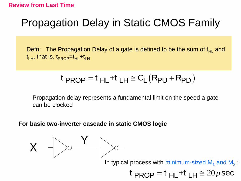
Propagation Delay in Static CMOS Family
Defn: The Propagation Delay of a gate is defined to be the sum of tHL and
tLH, that is, tPROP=tHL+tLH
PROP HL LH L PU PDt t +t C R R
XY
For basic two-inverter cascade in static CMOS logic
20PROP HL LHt t +t secp
Propagation delay represents a fundamental limit on the speed a gate
can be clocked
In typical process with minimum-sized M1 and M2 :
Review from Last Time

Propagation Delay in Static CMOS Family
F
A
Propagation through k levels of logic
HL HLk LH(k-1) XY1HL k-2t t + t + t + ••• + t
LH LHk HL(k-1) YX1LH k-2t t + t + t + ••• + t
where x=H and Y=L if k odd and X=L and Y=h if k even
1 PROP PROPkt t
k
i
Will return to propagation delay after we discuss device sizing
Review from Last Time
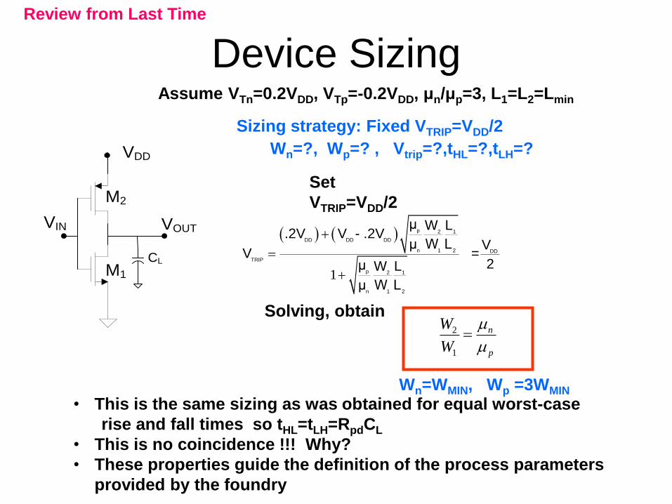
Device Sizing
1
p 2 1
DD DD DD
n 1 2 DD
TRIP
p 2 1
n 1 2
μ W L.2V V - .2V
μ W L VV =
2μ W L
μ W L
Set
VTRIP=VDD/2
Solving, obtain
Sizing strategy: Fixed VTRIP=VDD/2
• This is the same sizing as was obtained for equal worst-case
rise and fall times so tHL=tLH=RpdCL
• This is no coincidence !!! Why?
• These properties guide the definition of the process parameters
provided by the foundry
2
1
n
p
W
W
M1
M2
VDD
VIN VOUT
CL
Assume VTn=0.2VDD, VTp=-0.2VDD, μn/μp=3, L1=L2=Lmin
Wn=?, Wp=? , Vtrip=?,tHL=?,tLH=?
Wn=WMIN, Wp =3WMIN
Review from Last Time
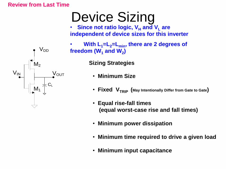
Device Sizing
• Minimum Size
• Fixed VTRIP (May Intentionally Differ from Gate to Gate)
• Equal rise-fall times
(equal worst-case rise and fall times)
• Minimum power dissipation
• Minimum time required to drive a given load
• Minimum input capacitance
Sizing Strategies
• Since not ratio logic, VH and VL are
independent of device sizes for this inverter
• With L1=L2=Lmin, there are 2 degrees of
freedom (W1 and W2)
M1
M2
VDD
VIN VOUT
CL
Review from Last Time

Device Sizing
Sizing Strategy Summary
Minimum Size VTRIP=VDD/2 Equal
Rise/Fall
Size Wn=Wp=Wmin
Lp=Ln=Lmin
Wn=Wmin
Wp=3Wmin
Lp=Ln=Lmin
Wn=Wmin
Wp=3Wmin
Lp=Ln=Lmin
tHL RpdCL RpdCL RpdCL
tLH 3RpdCL RpdCL RpdCL
tPROP 4RpdCL 2RpdCL 2RpdCL
Vtrip VTRIP=0.42VDD VTRIP=0.5VDD VTRIP=0.5VDD
M1
M2
VDD
VIN VOUT
CL
Assume VTn=0.2VDD, VTp=-0.2VDD, μn/μp=3, L1=L2=Lmin
• For a fixed load CL, the minimum-sized structure has a higher tPROP but if the load is
another inverter, CL will also change so the speed improvements become less apparent
• This will be investigated later

Reference InverterAssume μn/μp=3
Ln=Lp=LMIN
Wn=WMIN, Wp=3WnThe reference inverter
VIN VOUT
M1
M2
VDD
CL
• Have sized the reference inverter with Wp/Wn=μn/μp
• In standard processes, provides VTRIP ≈ VDD/2 and tHL ≈
tLH
• Any other sizing strategy could have been used for the
reference inverter but this is most convenient
REF INREF OX MIN MINdef
C = C = 4C W L
Tn DDV =.2VMIN MIN
PDREF
n OX MIN DD Tn n OX MIN DD
L LR
μ C W V -V μ C W 0.8V
Tp DDV = -.2V
MINPUREF PDREF
p OX MIN DD Tp
LR R
μ C 3W V +V

Reference InverterAssume μn/μp=3
Ln=Lp=LMIN
Wn=WMIN, Wp=3WnThe reference inverter pair
L1 REF OX MIN MINC = C =4C W L
VIN
VOUT
M1
M2
VDD
M1
M2
VDD
CL
V’OUT
CL1
REF PROPREF HLREF LHREF PDREF REFdef
t = t = t +t =2R C

Reference Inverter
REF OX MIN MINC = 4C W L
Assume μn/μp=3
Ln=Lp=LMIN
Wn=WMIN, Wp=3Wn
REF PDREF REFt =2R C
The reference inverter pair
REF OX MIN MINC =4C W L
VIN
VOUT
M1
M2
VDD
M1
M2
VDD
CL
V’OUT
CL1
Summary: parameters defined from reference inverter:
VIN VOUT
M1
M2
VDD
CL
MIN
PDREF
n OX MIN DD Tn
LR =
μ C W V -V

The Reference Inverter
REF IN OX MIN MINC =C = 4C W L
REF HLREF LHREF PDREF REFt = t + t = 2R C
VIN
VOUT
M1
M2
VDD
Wn=WMIN, Wp=3WMIN
Assume μn/μp=3
Reference Inverter
Ln=Lp=LMIN
In 0.5u proc tREF=20ps,
CREF=4fF, RPDREF=RPUREF=2.5K
HLREF LHREF PDREF REFt = t = R C
(Note: This COX is somewhat larger than that in the 0.5u ON process)
PDREF PUREFR =R
.2MIN MIN
PDREF
n OX MIN DD Tn n OX MIN DD
L LR =
μ C W V -V μ C W 0.8V
Tn DDV V
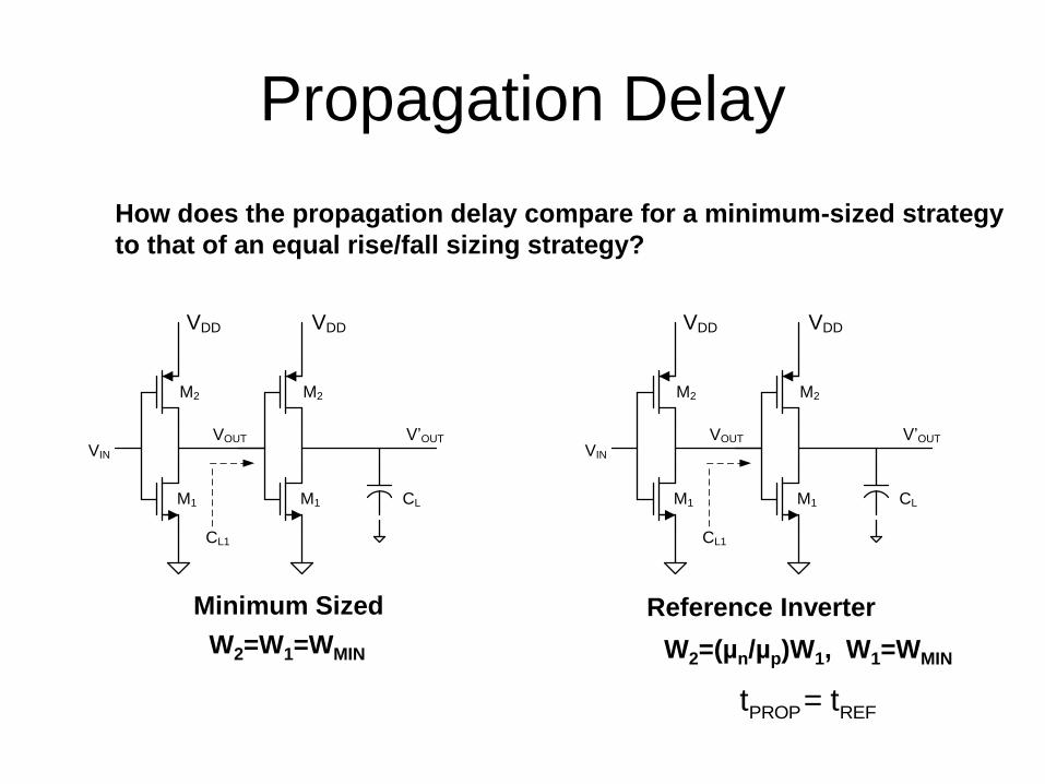
Propagation Delay
How does the propagation delay compare for a minimum-sized strategy
to that of an equal rise/fall sizing strategy?
VIN
VOUT
M1
M2
VDD
M1
M2
VDD
CL
V’OUT
CL1
VIN
VOUT
M1
M2
VDD
M1
M2
VDD
CL
V’OUT
CL1
Minimum Sized Reference Inverter
W2=W1=WMIN W2=(µn/µp)W1, W1=WMIN
PROP REFt = t

Device Sizing
REF OX MIN MINC = 4C W L
.2
0.8PDREFR
Tn DDV VMIN MIN
n OX MIN DD Tn n OX MIN DD
L L
C W V V C W V
Assume μn/μp=3
Ln=Lp=LMIN
Wn=WMIN, Wp=Wn
2PROP HLREF LHREF PDREF REF PDREF REF PDREF REFt =t +t =R 0.5C 3R 0.5C R C
The minimum-sized inverter pair
L1 REF OX MIN MINC = 0.5C =2C W LVIN
VOUT
M1
M2
VDD
M1
M2
VDD
CL
V’OUT
CL1
P R O P R E F Ft = t

By how much did tHL improve?
Why was there no net change in tPROP?
Propagation DelayHow does the propagation delay compare for a minimum-sized strategy
to that of an equal rise/fall sizing strategy?
VIN
VOUT
M1
M2
VDD
M1
M2
VDD
CL
V’OUT
CL1
VIN
VOUT
M1
M2
VDD
M1
M2
VDD
CL
V’OUT
CL1
Minimum Sized Reference Inverter
W2=W1=WMINW2=(µn/µp)W1, W1=WMIN
PROP REFt = tPROP REFt = t
Even though the tLH rise time has been reduced with the equal rise/fall sizing
strategy, this was done at the expense of an increase in the total load
capacitance that resulted in no net change in propagation delay!
They are the same!

Device Sizing
VINVOUT
M1
M2
VDD
VOUT
VDD
A1 A2 Ak
A1
A2
Ak
M11 M12 M1k
M21
M22
M2k
VOUT
M1k
M21
VDD
A1 A2 AkM22 M2k
A1
A2
Ak
M2k
M1k
Will consider now the multiple-input gates
Will consider both minimum sizing and equal worst-case rise/fall
Will assume CL (not shown)=CREF
Note: worst-case has been added since fall time in NOR gates or rise
time in NAND gates depends upon how many transistors are conducting
Will initially size so gate drive capability is same as that of ref inverter

Fan In• The Fan In (FI) to an input of a gate device, circuit or interconnect
that is capacitive is the input capacitance
• Often this is normalized to some capacitance (typically CREF of ref inverter).
ININ
REF
CFI =C alternately FI
C

Sizing of Multiple-Input Gates
Analysis strategy : Express delays in terms of those of reference inverter
IN REF OX MIN MINC =C = 4C W L
REF HLREF LHREF PDREF REFt = t + t = 2R C
MIN
PDREF PUREF
n OX MIN DD
LR R
μ C W 0.8VVIN
VOUT
M1
M2
VDD
Wn=WMIN, Wp=3WMIN
Assume μn/μp=3
Reference Inverter
Ln=Lp=LMIN
In 0.5u proc tREF=20ps,
CREF=4fF,RPDREF=2.5K
HLREF LHREF PDREF REFt = t =R C
INREF REF REF
REF
CFI =C alternately FI =1
C

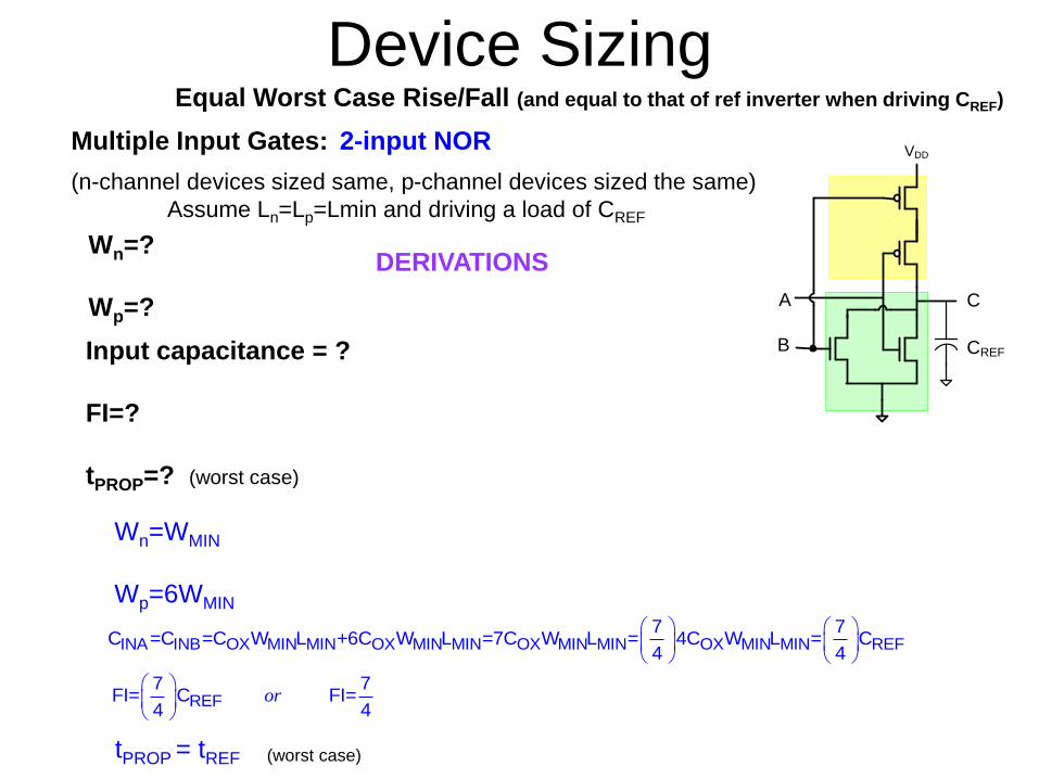
Device SizingMultiple Input Gates:
2-input NOR
Fastest response (tHL or tLH) = ?
Wn=?
Wp=?
Equal Worst Case Rise/Fall (and equal to that of ref inverter when driving CREF)
Input capacitance (FI) = ?
Minimum Sized (assume driving a load of CREF)
Wn=Wmin
Wp=Wmin
Fastest response (tHL or tLH) = ?
Slowest response (tHL or tLH) = ?
Input capacitance (FI) = ?
Worst case response (tPROP, usually of most interest)?
Worst case response (tPROP, usually of most interest)?
2-input NAND k-input NOR k-input NAND
A
B
C
VDD
CREF
VOUT
VDD
A1 A2 Ak
A1
A2
Ak
M11 M12 M1k
M21
M22
M2k
CREF
VDD
B
A C
CREF
VOUT
M1k
M21
VDD
A1 A2 AkM22 M2k
A1
A2
Ak
M2k
M1k
CREF
Device Sizing
Multiple Input Gates: 2-input NOR
DERIVATIONSWn=?
Wp=?
Equal Worst Case Rise/Fall (and equal to that of ref inverter when driving CREF)
Input capacitance = ?
FI=?
tPROP=? (worst case)
(n-channel devices sized same, p-channel devices sized the same)
Assume Ln=Lp=Lmin and driving a load of CREF
A
B
C
VDD
CREF
Wn=WMIN
Wp=6WMIN
INA INB OX MIN MIN OX MIN MIN OX MIN MIN OX MIN MIN REF7 7
C =C =C W L +6C W L =7C W L = 4C W L = C4 4
REF7 7
FI= C FI=4 4
or
tPROP = tREF (worst case)
One degree of freedom was used to
satisfy the constraint indicated
Other degree of freedom was used to
achieve equal rise and fall times

Device Sizing
Multiple Input Gates: k-input NOR
DERIVATIONS
Equal Worst Case Rise/Fall (and equal to that of ref inverter when driving CREF)
Wn=?
Wp=?
Input capacitance = ?
FI=?
tPROP=?
Wn=WMIN
Wp=3kWMIN
INx OX MIN MIN OX MIN MIN OX MIN MIN OX MIN MIN REF3k+1 3k+1
C =C W L +3kC W L = 3k+1 C W L = 4C W L = C4 4
REF3k+1 3k+1
FI= C FI=4 4
or
tPROP= tREF
VOUT
VDD
A1 A2 Ak
A1
A2
Ak
M11 M12 M1k
M21
M22
M2k
CREF

Device Sizing
Multiple Input Gates: 2-input NAND
DERIVATIONS
Equal Worst Case Rise/Fall (and equal to that of ref inverter when driving CREF)
Wn=?
Wp=?
Input capacitance = ?
FI=?
tPROP=?
VDD
B
A C
CREF
Wn=2WMIN
Wp=3WMIN
INA INB OX MIN MIN OX MIN MIN OX MIN MIN OX MIN MIN REF5 5
C =C =2C W L +3C W L = 5 C W L = 4C W L = C4 4
REF5 5
FI= C FI=4 4
or
tPROP= tREF

Device Sizing
Multiple Input Gates: k-input NAND
DERIVATIONS
Equal Worst Case Rise/Fall (and equal to that of ref inverter when driving CREF)
Wn=?
Wp=?
Input capacitance = ?
FI=?
tPROP=?
Wn=kWMIN
Wp=3WMIN
INx OX MIN MIN OX MIN MIN OX MIN MIN OX MIN MIN REF3+k 3+k
C =kC W L +3C W L = 3+k C W L = 4C W L = C4 4
REF3+k 3+k
FI= C FI=4 4
or
tPROP= tREF
VOUT
M1k
M21
VDD
A1 A2 AkM22 M2k
A1
A2
Ak
M2k
M1k
CREF
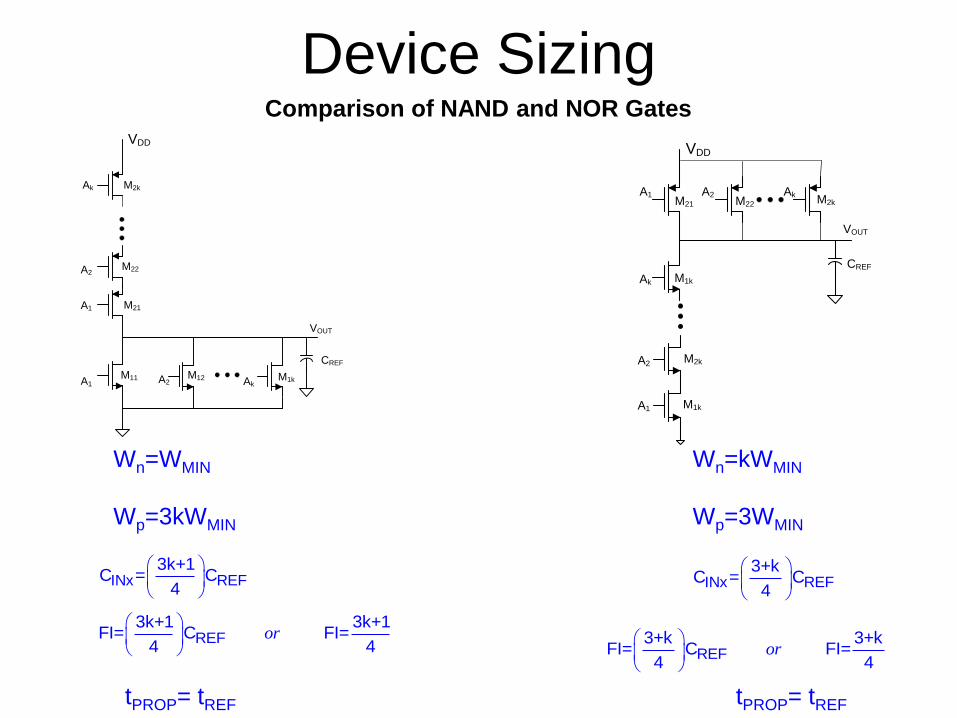
Device SizingComparison of NAND and NOR Gates
INx REF3+k
C = C4
REF3+k 3+k
FI= C FI=4 4
or
Wn=kWMIN
Wp=3WMIN
Wn=WMIN
Wp=3kWMIN
INx REF3k+1
C = C4
REF3k+1 3k+1
FI= C FI=4 4
or
tPROP= tREF tPROP= tREF
VOUT
VDD
A1 A2 Ak
A1
A2
Ak
M11 M12 M1k
M21
M22
M2k
CREF
VOUT
M1k
M21
VDD
A1 A2 AkM22 M2k
A1
A2
Ak
M2k
M1k
CREF

Device Sizing
IN REFC =C
Assume μn/μp=3
Ln=Lp=LMIN
Wn=WMIN, Wp=3WMIN
Equal Worse-Case Rise/Fall Device Sizing Strategy
-- (same as VTRIP=VDD/2 for worst case delay in typical process considered in example)
k-input NANDINV k-input NOR
Wn=WMIN, Wp=3kWMINWn=kWMIN, Wp=3WMIN
IN REF
3k+1C = C
4
IN REF
3+kC = C
4
VIN
VOUT
M1
M2
VDD
CREF
VOUT
M1k
M21
VDD
A1 A2 AkM22 M2k
A1
A2
Ak
M2k
M1k
CREF
VOUT
VDD
A1 A2 Ak
A1
A2
Ak
M11 M12 M1k
M21
M22
M2k
CREF
FI=1
3k+1FI=
4
3+kFI=
4
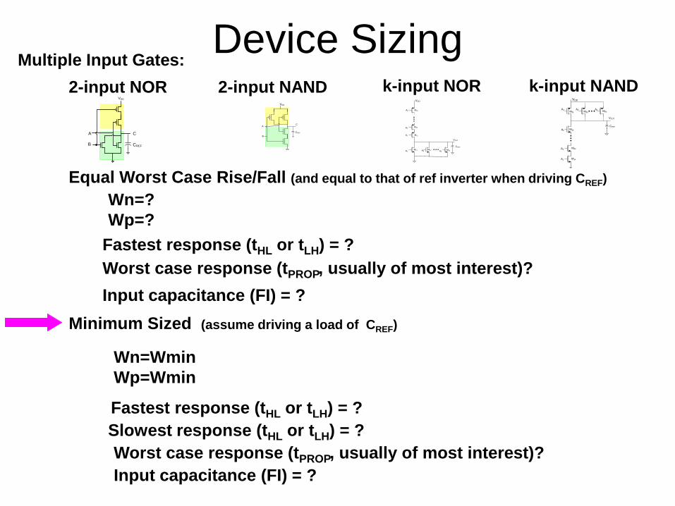
Device SizingMultiple Input Gates:
2-input NOR
Fastest response (tHL or tLH) = ?
Wn=?
Wp=?
Equal Worst Case Rise/Fall (and equal to that of ref inverter when driving CREF)
Input capacitance (FI) = ?
Minimum Sized (assume driving a load of CREF)
Wn=Wmin
Wp=Wmin
Fastest response (tHL or tLH) = ?
Slowest response (tHL or tLH) = ?
Input capacitance (FI) = ?
Worst case response (tPROP, usually of most interest)?
Worst case response (tPROP, usually of most interest)?
2-input NAND k-input NOR k-input NAND
A
B
C
VDD
CREF
VOUT
VDD
A1 A2 Ak
A1
A2
Ak
M11 M12 M1k
M21
M22
M2k
CREF
VDD
B
A C
CREF
VOUT
M1k
M21
VDD
A1 A2 AkM22 M2k
A1
A2
Ak
M2k
M1k
CREF

Device Sizing
Minimum Sized (assume driving a load of CREF) Wn=Wmin Wp=Wmin
Fastest response (tHL or tHL) = ?
Slowest response (tHL or tHL) = ?
Input capacitance (FI) = ?
Worst case response (tPROP, usually of most interest)?
VOUT
VDD
A1 A2 Ak
A1
A2
Ak
M11 M12 M1k
M21
M22
M2k
CREF
VOUT
M1k
M21
VDD
A1 A2 AkM22 M2k
A1
A2
Ak
M2k
M1k
CREF
A
B
C
VDD
CREF
VDD
B
A C
CREF
VIN
VOUT
M1
M2
VDD
CREF
REFIN OX n n OX p p OX min min OX min min ox min min
CC = C W L +C W L = C W L + C W L = 2C W L =
21
FI =2

Device Sizing – minimum size driving CREF
k-input NANDINV
k-input NOR
PROPt ?PROPt ?
PROP
3t 0.5
2REF REF
kt t
PROP
3 1t
2REF
kt
PROP
3t
2 2REF REF
kt t
PROP
3t
2REF
kt
REFC
FI = 2
REFC
FI = 2
3PU PDREFR kRPD PDREFR R PU PD PDREFR R R3PD PDREFR R 3PU PDREFR R
VOUT
M1k
M21
VDD
A1 A2 AkM22 M2k
A1
A2
Ak
M2k
M1k
CREF
VIN
VOUT
M1
M2
VDD
CREF VOUT
VDD
A1 A2 Ak
A1
A2
Ak
M11 M12 M1k
M21
M22
M2k
CREF
REFC
FI = 2
PROPt ?
PROPt 2 REFt
PROP
3t 0.5
2REF REFt t
Digital Circuit Design
• Hierarchical Design
• Basic Logic Gates
• Properties of Logic Families
• Characterization of CMOS
Inverter
• Static CMOS Logic Gates
– Ratio Logic
• Propagation Delay
– Simple analytical models
– Elmore Delay
• Sizing of Gates
• Propagation Delay with
Multiple Levels of Logic
• Optimal driving of Large
Capacitive Loads
• Power Dissipation in Logic
Circuits
• Other Logic Styles
• Array Logic
• Ring Oscillators

Device Sizing Summary
k-input NANDINV k-input NOR
CIN for NAND gates is considerably smaller than for NOR gates for
equal worst-case rise and fall times
CIN for minimuim-sized structures is independent of number of
inputs and much smaller than CIN for the equal rise/fall time case
RPU gets very large for minimum-sized NOR gate
VOUT
VDD
A1 A2 Ak
A1
A2
Ak
M11 M12 M1k
M21
M22
M2k
CREF
VIN
VOUT
M1
M2
VDD
CREF
VOUT
M1k
M21
VDD
A1 A2 AkM22 M2k
A1
A2
Ak
M2k
M1k
CREF
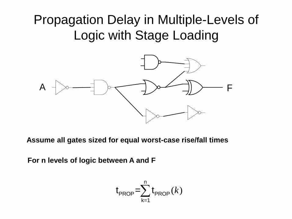
Propagation Delay in Multiple-Levels of
Logic with Stage Loading
A F
( )n
PROP PROP
k=1
t = t k
For n levels of logic between A and F
Assume all gates sized for equal worst-case rise/fall times
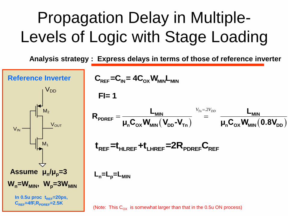
Propagation Delay in Multiple-
Levels of Logic with Stage Loading
Analysis strategy : Express delays in terms of those of reference inverter
REF IN OX MIN MINC =C = 4C W L
REF HLREF LHREF PDREF REFt =t +t =2R C
.2MIN MIN
PDREF
n OX MIN DD Tn n OX MIN DD
L LR
μ C W V -V μ C W 0.8V
Tn DDV V
VIN
VOUT
M1
M2
VDD
Wn=WMIN, Wp=3WMIN
Assume μn/μp=3
Reference Inverter
Ln=Lp=LMIN
In 0.5u proc tREF=20ps,
CREF=4fF,RPDREF=2.5K
FI= 1
(Note: This COX is somewhat larger than that in the 0.5u ON process)

Propagation Delay in Multiple-Levels of
Logic with Stage Loading
A F
What loading will a gate see?
• Input capacitance to other gates
• Any load capacitors
• Parasitic interconnect capacitnaces
Assume:
• all gates sized for equal worst-case rise/fall times
• all gates sized to have rise and fall times equal to that of ref
inverter when driving CREF
Observe:
• Propagation delay of these gates will be scaled by the ratio of the
total load capacitance on each gate to CREF

Propagation Delay with Stage Loading
REF OX MIN MINC = 4C W L
REF PDref REFt =2R CVIN
VOUT
FI of a capacitor
FI of a gate (input k)
C
REF
CFI =
C
INkG
REF
CFI =
C
INII
REF
CFI =
CFI of an interconnect
Overall FI INGi INCi INIi
Gates Capacitances Interconnects
REF
C + C + C
FI = C
FI can be expressed either in units of capacitance or normalized to CREF
Most commonly FI is normalized but must determine from context
prop-k REF LOADt = t FIIf gates sized to have same drive as ref inverter

End of Lecture 39