Fundamentals of Modern VLSI Devices -...
23
Fundamentals of Modern VLSI Devices Learn the basic properties and designs of modern VLSI devices, as well as the factors affecting performance, with this thoroughly updated second edition. The first edition has been widely adopted as a standard textbook in microelectronics in many major US universities and worldwide. The internationally renowned authors highlight the intricate interdependencies and subtle tradeoffs between various practically important device parameters. An in-depth discussion of device scaling and scaling limits of CMOS and bipolar devices is also provided. Equations and parameters provided are checked con- tinuously against the reality of silicon data, making the book equally useful in practical transistor design and in the classroom. New to this edition: Every chapter has been updated to include the latest developments, such as MOSFET scale length theory, high-field transport models, and SiGe-base bipolar devices. Two new chapters cover read and write operations of commonly used SRAM, DRAM, and non-volatile memory arrays, as well as silicon-on-insulator (SOI) devices, including advanced devices of future potential. More useful appendices: The number has doubled from 9 to 18, covering areas such as spatial variation of quasi-Fermi potentials, image-force-induced barrier lowering, and power gain of a two-port network. New homework exercises at the end of every chapter engage students with real-world problems and test their understanding. YUAN TAUR is Professor of Electrical and Computer Engineering at the University of California, San Diego. He spent 20 years at IBM’ s T. J. Watson Research Center where he won numerous invention and achievement awards. He is an IEEE Fellow, Editor-in- Chief of IEEE Electron Device Letters, and holds 14 US patents. TAK H . NING is an IBM Fellow at the T.J. Watson Research Center, New York, where he has worked for over 35 years. A Fellow of the IEEE and the American Physical Society, and a member of the US National Academy of Engineering, he has authored more than 120 technical papers and holds 36 US patents. He has won several awards, including the ECS 2007 Gordon E. Moore Medal, the IEEE 1991 Jack A. Morton Award, and the 1998 Pan Wen-Yuan Foundation Outstanding Research Award. www.cambridge.org © in this web service Cambridge University Press Cambridge University Press 978-0-521-83294-6 - Fundamentals of Modern VLSI Devices: Second Edition Yuan Taur and Tak H. Ning Frontmatter More information
Transcript of Fundamentals of Modern VLSI Devices -...

Fundamentals of Modern VLSI Devices
Learn the basic properties and designs of modern VLSI devices, as well as the factorsaffecting performance, with this thoroughly updated second edition. The first edition hasbeen widely adopted as a standard textbook in microelectronics in many major USuniversities and worldwide. The internationally renowned authors highlight the intricateinterdependencies and subtle tradeoffs between various practically important deviceparameters. An in-depth discussion of device scaling and scaling limits of CMOS andbipolar devices is also provided. Equations and parameters provided are checked con-tinuously against the reality of silicon data, making the book equally useful in practicaltransistor design and in the classroom.
New to this edition:
� Every chapter has been updated to include the latest developments, such asMOSFETscale length theory, high-field transport models, and SiGe-base bipolar devices.
� Two new chapters cover read and write operations of commonly used SRAM,DRAM, and non-volatile memory arrays, as well as silicon-on-insulator (SOI)devices, including advanced devices of future potential.
� More useful appendices: The number has doubled from 9 to 18, covering areas suchas spatial variation of quasi-Fermi potentials, image-force-induced barrier lowering,and power gain of a two-port network.
� New homework exercises at the end of every chapter engage students with real-worldproblems and test their understanding.
Y U A N T A U R is Professor of Electrical and Computer Engineering at the University ofCalifornia, San Diego. He spent 20 years at IBM’s T. J. Watson Research Center where hewon numerous invention and achievement awards. He is an IEEE Fellow, Editor-in-Chief of IEEE Electron Device Letters, and holds 14 US patents.
T A K H . N I N G is an IBM Fellow at the T. J. Watson Research Center, New York, wherehe has worked for over 35 years. A Fellow of the IEEE and the American PhysicalSociety, and a member of the US National Academy of Engineering, he has authoredmore than 120 technical papers and holds 36 US patents. He has won several awards,including the ECS 2007 Gordon E. Moore Medal, the IEEE 1991 Jack A.Morton Award,and the 1998 Pan Wen-Yuan Foundation Outstanding Research Award.
www.cambridge.org© in this web service Cambridge University Press
Cambridge University Press978-0-521-83294-6 - Fundamentals of Modern VLSI Devices: Second EditionYuan Taur and Tak H. NingFrontmatterMore information

www.cambridge.org© in this web service Cambridge University Press
Cambridge University Press978-0-521-83294-6 - Fundamentals of Modern VLSI Devices: Second EditionYuan Taur and Tak H. NingFrontmatterMore information

Fundamentals of ModernVLSI Devices
SECOND EDIT ION
YUAN TAURUniversity of California, San Diego
TAK H. NINGIBM T. J. Watson Research Center, New York
www.cambridge.org© in this web service Cambridge University Press
Cambridge University Press978-0-521-83294-6 - Fundamentals of Modern VLSI Devices: Second EditionYuan Taur and Tak H. NingFrontmatterMore information
www.cambridge.orgInformation on this title: www.cambridge.org/9780521832946
© Cambridge University Press 1998, 2009
This publication is in copyright. Subject to statutory exceptionand to the provisions of relevant collective licensing agreements,no reproduction of any part may take place withoutthe written permission of Cambridge University Press.
First published 1998Second edition 2009First paperback edition 20133rd printing 2015
Printed in the United Kingdom by Clays, St Ives plc.
A catalog record for this publication is available from the British Library
Library of Congress Cataloging in Publication dataTaur, Yuan, 1946–Fundamentals of modern VLSI devices / Yuan Taur, Tak H. Ning. – 2nd ed.p. cm.
ISBN 978-0-521-83294-61. Metal oxide semiconductors, Complementary. 2. Bipolar transistors.3. Integrated circuits – Very large scale integration.I. Ning, Tak H., 1943– II. Title.TK7871.99.M44T38 2009621.39′5–dc22
2009007334
ISBN 978-0-521-83294-6 hardbackISBN 978-1-107-63571-5 Paperback
Cambridge University Press has no responsibility for the persistence oraccuracy of URLs for external or third-party Internet websites referred toin this publication, and does not guarantee that any content on suchwebsites is, or will remain, accurate or appropriate.
University Printing House, Cambridge CB2 8BS, United Kingdom
Cambridge University Press is part of the University of Cambridge.
It furthers the University,’s mission by disseminating knowledge in the pursuit of
education, learning and research at the highest international levels of excellence.
www.cambridge.org© in this web service Cambridge University Press
Cambridge University Press978-0-521-83294-6 - Fundamentals of Modern VLSI Devices: Second EditionYuan Taur and Tak H. NingFrontmatterMore information
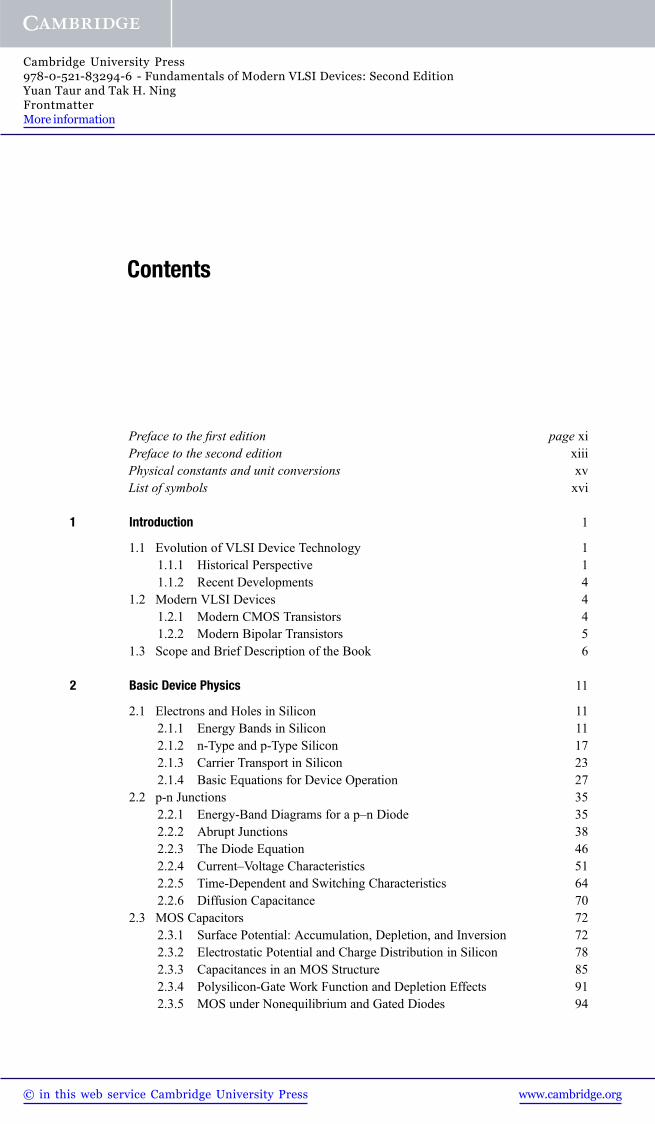
Contents
Preface to the first edition page xiPreface to the second edition xiiiPhysical constants and unit conversions xvList of symbols xvi
1 Introduction 1
1.1 Evolution of VLSI Device Technology 11.1.1 Historical Perspective 11.1.2 Recent Developments 4
1.2 Modern VLSI Devices 41.2.1 Modern CMOS Transistors 41.2.2 Modern Bipolar Transistors 5
1.3 Scope and Brief Description of the Book 6
2 Basic Device Physics 11
2.1 Electrons and Holes in Silicon 112.1.1 Energy Bands in Silicon 112.1.2 n-Type and p-Type Silicon 172.1.3 Carrier Transport in Silicon 232.1.4 Basic Equations for Device Operation 27
2.2 p-n Junctions 352.2.1 Energy-Band Diagrams for a p–n Diode 352.2.2 Abrupt Junctions 382.2.3 The Diode Equation 462.2.4 Current–Voltage Characteristics 512.2.5 Time-Dependent and Switching Characteristics 642.2.6 Diffusion Capacitance 70
2.3 MOS Capacitors 722.3.1 Surface Potential: Accumulation, Depletion, and Inversion 722.3.2 Electrostatic Potential and Charge Distribution in Silicon 782.3.3 Capacitances in an MOS Structure 852.3.4 Polysilicon-Gate Work Function and Depletion Effects 912.3.5 MOS under Nonequilibrium and Gated Diodes 94
www.cambridge.org© in this web service Cambridge University Press
Cambridge University Press978-0-521-83294-6 - Fundamentals of Modern VLSI Devices: Second EditionYuan Taur and Tak H. NingFrontmatterMore information
2.3.6 Charge in Silicon Dioxide and at the Silicon–Oxide Interface 982.3.7 Effect of Interface Traps and Oxide Charge on Device Characteristics 103
2.4 Metal–Silicon Contacts 1082.4.1 Static Characteristics of a Schottky Barrier Diode 1082.4.2 Current Transport in a Schottky Barrier Diode 1152.4.3 Current–Voltage Characteristics of a Schottky Barrier Diode 1152.4.4 Ohmic Contacts 120
2.5 High-Field Effects 1222.5.1 Impact Ionization and Avalanche Breakdown 1222.5.2 Band-to-Band Tunneling 1252.5.3 Tunneling into and through Silicon Dioxide 1272.5.4 Injection of Hot Carriers from Silicon into Silicon Dioxide 1332.5.5 High-Field Effects in Gated Diodes 1352.5.6 Dielectric Breakdown 137Exercises 141
3 MOSFET Devices 148
3.1 Long-Channel MOSFETs 1483.1.1 Drain-Current Model 1493.1.2 MOSFET I–V Characteristics 1553.1.3 Subthreshold Characteristics 1633.1.4 Substrate Bias and Temperature Dependence of Threshold Voltage 1663.1.5 MOSFET Channel Mobility 1693.1.6 MOSFET Capacitances and Inversion-Layer Capacitance Effect 172
3.2 Short-Channel MOSFETs 1753.2.1 Short-Channel Effect 1763.2.2 Velocity Saturation and High-Field Transport 1863.2.3 Channel Length Modulation 1953.2.4 Source–Drain Series Resistance 1963.2.5 MOSFET Degradation and Breakdown at High Fields 196Exercises 201
4 CMOS Device Design 204
4.1 MOSFET Scaling 2044.1.1 Constant-Field Scaling 2044.1.2 Generalized Scaling 2074.1.3 Nonscaling Effects 210
4.2 Threshold Voltage 2124.2.1 Threshold-Voltage Requirement 2134.2.2 Channel Profile Design 2174.2.3 Nonuniform Doping 2244.2.4 Quantum Effect on Threshold Voltage 2344.2.5 Discrete Dopant Effects on Threshold Voltage 239
vi Contents
www.cambridge.org© in this web service Cambridge University Press
Cambridge University Press978-0-521-83294-6 - Fundamentals of Modern VLSI Devices: Second EditionYuan Taur and Tak H. NingFrontmatterMore information
4.3 MOSFET Channel Length 2424.3.1 Various Definitions of Channel Length 2424.3.2 Extraction of the Effective Channel Length 2444.3.3 Physical Meaning of Effective Channel Length 2484.3.4 Extraction of Channel Length by C–V Measurements 252Exercises 254
5 CMOS Performance Factors 256
5.1 Basic CMOS Circuit Elements 2565.1.1 CMOS Inverters 2565.1.2 CMOS NAND and NOR Gates 2665.1.3 Inverter and NAND Layouts 270
5.2 Parasitic Elements 2735.2.1 Source–Drain Resistance 2745.2.2 Parasitic Capacitances 2775.2.3 Gate Resistance 2805.2.4 Interconnect R and C 283
5.3 Sensitivity of CMOS Delay to Device Parameters 2895.3.1 Propagation Delay and Delay Equation 2895.3.2 Delay Sensitivity to Channel Width, Length, and Gate Oxide Thickness 2965.3.3 Sensitivity of Delay to Power-Supply Voltage and Threshold Voltage 2995.3.4 Sensitivity of Delay to Parasitic Resistance and Capacitance 3015.3.5 Delay of Two-Way NAND and Body Effect 304
5.4 Performance Factors of Advanced CMOS Devices 3075.4.1 MOSFETs in RF Circuits 3085.4.2 Effect of Transport Parameters on CMOS Performance 3115.4.3 Low-Temperature CMOS 312Exercises 315
6 Bipolar Devices 318
6.1 n–p–n Transistors 3186.1.1 Basic Operation of a Bipolar Transistor 3226.1.2 Modifying the Simple Diode Theory for Describing Bipolar Transistors 322
6.2 Ideal Current–Voltage Characteristics 3276.2.1 Collector Current 3296.2.2 Base Current 3306.2.3 Current Gains 3346.2.4 Ideal IC–VCE Characteristics 336
6.3 Characteristics of a Typical n–p–n Transistor 3376.3.1 Effect of Emitter and Base Series Resistances 3386.3.2 Effect of Base–Collector Voltage on Collector Current 3406.3.3 Collector Current Falloff at High Currents 3436.3.4 Nonideal Base Current at Low Currents 347
Contents vii
www.cambridge.org© in this web service Cambridge University Press
Cambridge University Press978-0-521-83294-6 - Fundamentals of Modern VLSI Devices: Second EditionYuan Taur and Tak H. NingFrontmatterMore information
6.4 Bipolar Device Models for Circuit and Time-Dependent Analyses 3526.4.1 Basic dc Model 3526.4.2 Basic ac Model 3556.4.3 Small-Signal Equivalent-Circuit Model 3566.4.4 Emitter Diffusion Capacitance 3596.4.5 Charge-Control Analysis 361
6.5 Breakdown Voltages 3666.5.1 Common-Base Current Gain in the Presence of Base–Collector
Junction Avalanche 3676.5.2 Saturation Currents in a Transistor 3696.5.3 Relation Between BVCEO and BVCBO 370Exercises 371
7 Bipolar Device Design 374
7.1 Design of the Emitter Region 3747.1.1 Diffused or Implanted-and-Diffused Emitter 3757.1.2 Polysilicon Emitter 376
7.2 Design of the Base Region 3777.2.1 Relationship between Base Sheet Resistivity and Collector
Current Density 3787.2.2 Intrinsic-Base Dopant Distribution 3807.2.3 Electric Field in the Quasineutral Intrinsic Base 3817.2.4 Base Transit Time 384
7.3 Design of the Collector Region 3857.3.1 Collector Design When There Is Negligible Base Widening 3877.3.2 Collector Design When There Is Appreciable Base Widening 388
7.4 SiGe-Base Bipolar Transistors 3897.4.1 Transistors Having a Simple Linearly Graded Base Bandgap 3907.4.2 Base Current When Ge Is Present in the Emitter 3967.4.3 Transistors Having a Trapezoidal Ge Distribution in the Base 4017.4.4 Transistors Having a Constant Ge Distribution in the Base 4067.4.5 Effect of Emitter Depth Variation on Device Characteristics 4107.4.6 Some Optimal Ge Profiles 4147.4.7 Base-Width Modulation by VBE 4197.4.8 Reverse–Mode I–V Characteristics 4237.4.9 Heterojunction Nature of a SiGe-Base Bipolar Transistor 426
7.5 Modern Bipolar Transistor Structures 4297.5.1 Deep-Trench Isolation 4297.5.2 Polysilicon Emitter 4307.5.3 Self-Aligned Polysilicon Base Contact 4307.5.4 Pedestal Collector 4317.5.5 SiGe-Base 431Exercises 432
viii Contents
www.cambridge.org© in this web service Cambridge University Press
Cambridge University Press978-0-521-83294-6 - Fundamentals of Modern VLSI Devices: Second EditionYuan Taur and Tak H. NingFrontmatterMore information

8 Bipolar Performance Factors 437
8.1 Figures of Merit of a Bipolar Transistor 4378.1.1 Cutoff Frequency 4378.1.2 Maximum Oscillation Frequency 4408.1.3 Ring Oscillator and Gate Delay 440
8.2 Digital Bipolar Circuits 4418.2.1 Delay Components of a Logic Gate 4428.2.2 Device Structure and Layout for Digital Circuits 445
8.3 Bipolar Device Optimization for Digital Circuits 4478.3.1 Design Points for a Digital Circuit 4478.3.2 Device Optimization When There Is Significant
Base Widening 4488.3.3 Device Optimization When There Is Negligible
Base Widening 4498.3.4 Device Optimization for Small Power–Delay Product 4538.3.5 Bipolar Device Optimization from Some Data Analyses 455
8.4 Bipolar Device Scaling for ECL Circuits 4578.4.1 Device Scaling Rules 4588.4.2 Limits in Bipolar Device Scaling for ECL Circuits 460
8.5 Bipolar Device Optimization and Scaling for RF and Analog Circuits 4638.5.1 The Single-Transistor Amplifier 4638.5.2 Optimizing the Individual Parameters 4648.5.3 Technology for RF and Analog Bipolar Devices 4678.5.4 Limits in Scaling Bipolar Transistors for RF and
Analog Applications 4688.6 Comparing a SiGe-Base Bipolar Transistor with a GaAs HBT 469
Exercises 472
9 Memory Devices 476
9.1 Static Random-Access Memory 4779.1.1 CMOS SRAM Cell 4789.1.2 Other Bistable MOSFET SRAM Cells 4869.1.3 Bipolar SRAM Cell 487
9.2 Dynamic Random-Access Memory 4959.2.1 Basic DRAM Cell and Its Operation 4969.2.2 Device Design and Scaling Considerations for a DRAM Cell 499
9.3 Nonvolatile Memory 5009.3.1 MOSFET Nonvolatile Memory Devices 5019.3.2 Flash Memory Arrays 5079.3.3 Floating-Gate Nonvolatile Memory Cells 5119.3.4 Nonvolatile Memory Cells with Charge Stored in Insulator 514Exercise 516
Contents ix
www.cambridge.org© in this web service Cambridge University Press
Cambridge University Press978-0-521-83294-6 - Fundamentals of Modern VLSI Devices: Second EditionYuan Taur and Tak H. NingFrontmatterMore information
10 Silicon-on-Insulator Devices 517
10.1 SOI CMOS 51710.1.1 Partially Depleted SOI MOSFETs 51810.1.2 Fully Depleted SOI MOSFETs 520
10.2 Thin-Silicon SOI Bipolar 52310.2.1 Fully Depleted Collector Mode 52410.2.2 Partially Depleted Collector Mode 52610.2.3 Accumulation Collector Mode 52710.2.4 Discussion 527
10.3 Double-Gate MOSFETs 52910.3.1 An Analytic Drain Current Model for Symmetric DG MOSFETs 52910.3.2 The Scale Length of Double-Gate MOSFETs 53310.3.3 Fabrication Requirements and Challenges of DG MOSFETs 53410.3.4 Multiple-Gate MOSFETs 536Exercise 537
Appendix 1 CMOS Process Flow 538Appendix 2 Outline of a Process for Fabricating Modern n–p–n Bipolar
Transistors 542Appendix 3 Einstein Relations 543Appendix 4 Spatial Variation of Quasi-Fermi Potentials 546Appendix 5 Generation and Recombination Processes and Space-Charge-
Region Current 553Appendix 6 Diffusion Capacitance of a p–n Diode 562Appendix 7 Image-Force-Induced Barrier Lowering 569Appendix 8 Electron-Initiated and Hole-Initiated Avalanche Breakdown 573Appendix 9 An Analytical Solution for the Short-Channel Effect in
Subthreshold 575Appendix 10 Generalized MOSFET Scale Length Model 582Appendix 11 Drain Current Model of a Ballistic MOSFET 588Appendix 12 Quantum-Mechanical Solution in Weak Inversion 594Appendix 13 Power Gain of a Two-Port Network 598Appendix 14 Unity-Gain Frequencies of a MOSFET Transistor 601Appendix 15 Determination of Emitter and Base Series Resistances 605Appendix 16 Intrinsic-Base Resistance 610Appendix 17 Energy-Band Diagram of a Si–SiGe n–p Diode 614Appendix 18 fT and fmax of a Bipolar Transistor 617References 623Index 644
x Contents
www.cambridge.org© in this web service Cambridge University Press
Cambridge University Press978-0-521-83294-6 - Fundamentals of Modern VLSI Devices: Second EditionYuan Taur and Tak H. NingFrontmatterMore information
Preface to the first edition
It has been fifty years since the invention of the bipolar transistor, more than forty yearssince the invention of the integrated-circuit (IC) technology, and more than thirty-fiveyears since the invention of the MOSFET. During this time, there has been a tremendousand steady progress in the development of the IC technology with a rapid expansion ofthe IC industry. One distinct characteristic in the evolution of the IC technology is that thephysical feature sizes of the transistors are reduced continually over time as the litho-graphy technologies used to define these features become available. For almost thirtyyears now, the minimum lithography feature size used in IC manufacturing has beenreduced at a rate of 0.7� every three years. In 1997, the leading-edge IC products have aminimum feature size of 0.25 μm.
The basic operating principles of large and small transistors are the same. However, therelative importance of the various device parameters and performance factors for tran-sistors of the 1- μm and smaller generations is quite different from those for transistors oflarger-dimension generations. For example, in the case of CMOS, the power-supplyvoltage was lowered from the standard 5V, starting with the 0.6- to 0.8- μm generation.Since then CMOS power supply voltage has been lowered in steps once every few yearsas the device physical dimensions are reduced. At the same time, many physicalphenomena, such as short-channel effect and velocity saturation, which are negligiblein large-dimension MOSFETs, are becoming more and more important in determiningthe behavior of MOSFETs of deep-submicron dimensions. In the case of bipolar devices,breakdown voltage and base-widening effects are limiting their performance, and powerdissipation is limiting their level of integration on a chip. Also, the advent of SiGe-base bipolar technology has extended the frequency capability of small-dimensionbipolar transistors into the range previously reserved for GaAs and other compound-semiconductor devices.
The purpose of this book is to bring together the device fundamentals that govern thebehavior of CMOS and bipolar transistors into a single text, with emphasis on thoseparameters and performance factors that are particularly important for VLSI (very-large-scale-integration) devices of deep-submicron dimensions. The book starts with a com-prehensive review of the properties of the silicon material, and the basic physics of p–njunctions and MOS capacitors, as they relate to the fundamental principles of MOSFETand bipolar transistors. From there, the basic operation of MOSFET and bipolar devices,and their design and optimization for VLSI applications are developed. A great deal ofthe volume is devoted to in-depth discussions of the intricate interdependence and subtletradeoffs of the various device parameters pertaining to circuit performance and manu-facturability. The effects which are particularly important in small-dimension devices,
www.cambridge.org© in this web service Cambridge University Press
Cambridge University Press978-0-521-83294-6 - Fundamentals of Modern VLSI Devices: Second EditionYuan Taur and Tak H. NingFrontmatterMore information

e.g., quantization of the two-dimensional surface inversion layer in a MOSFET deviceand the heavy-doping effect in the intrinsic base of a bipolar transistor, are covered indetail. Also included in this book are extensive discussions on scaling and limitations toscaling of MOSFET and bipolar devices.
This book is suitable for use as a textbook by senior undergraduate or graduatestudents in electrical engineering and microelectronics. The necessary backgroundassumed is an introductory understanding of solid-state physics and semiconductorphysics. For practicing engineers and scientists actively involved in research and devel-opment in the IC industry, this book serves as a reference in providing a body ofknowledge in modern VLSI devices for them to stay up to date in this field.
VLSI devices are too huge a subject area to cover thoroughly in one book. We havechosen to cover only the fundamentals necessary for discussing the design and optimiza-tion of the state-of-the-art CMOS and bipolar devices in the sub-0.5-μm regime. Eventhen, the specific topics covered in this book are based on our own experience of what themost important device parameters and performance factors are in modern VLSI devices.
Many people have contributed directly and indirectly to the topics covered in thisbook. We have benefited enormously from the years of collaboration and interaction wehad with our colleagues at IBM, particularly in the areas of advanced silicon-deviceresearch and development. These include Douglas Buchanan, Hu Chao, T. C. Chen, WeiChen, Kent Chuang, Peter Cook, Emmanuel Crabbé, John Cressler, Bijan Davari, RobertDennard, Max Fischetti, David Frank, Charles Hsu, Genda Hu, Randall Isaac, KhalidIsmail, G. P. Li, Shih-Hsien Lo, Yuh-Jier Mii, Edward Nowak, George Sai-Halasz,Stanley Schuster, Paul Solomon, Hans Stork, Jack Sun, Denny Tang, Lewis Terman,Clement Wann, James Warnock, Siegfried Wiedmann, Philip Wong, MatthewWordeman, Ben Wu, and Hwa Yu.
We would like to acknowledge the secretarial support of Barbara Grady and thesupport of our management at IBM Thomas J. Watson Research Center where thisbook was written. Finally, we would like to give special thanks to our families –
Teresa, Adrienne, and Brenda Ning and Betty, Ying, and Hsuan Taur – for their supportand understanding during this seemingly endless task.
Yuan TaurTak H. Ning
Yorktown Heights, New York, October, 1997
xii Preface to the first edition
www.cambridge.org© in this web service Cambridge University Press
Cambridge University Press978-0-521-83294-6 - Fundamentals of Modern VLSI Devices: Second EditionYuan Taur and Tak H. NingFrontmatterMore information
Preface to the second edition
Since the publication of the first edition of Fundamentals of Modern VLSI Devices byCambridge University Press in 1998, we received much praise and many encouragingreviews on the book. It has been adopted as a textbook for first-year graduate courses onmicroelectronics in many major universities in the United States and worldwide. The firstedition was translated into Japanese by a team led by Professor Shibahara of HiroshimaUniversity in 2002.
During the past 10 years, the evolution and scaling of VLSI (very-large-scale-integration) technology has continued. Now, sixty years after the first invention of thetransistor, the number of transistors per chip for both microprocessors and DRAM(dynamic random access memory) has increased to over one billion, and the highestclock frequency of microprocessors has reached 5GHz. In 2007, the worldwide IC(integrated circuits) sales grew to $250 billion. In 2008, the IC industry reached the45-nm generation, meaning that the leading-edge IC products employ a minimumlithography feature size of 45 nm. As bulk CMOS (complementary metal–oxide–semiconductor field-effect transistor) technologies are scaled to dimensions below100 nm, the very factor that makes CMOS technology the technology of choice fordigital VLSI circuits, namely, its low standby power, can no longer be taken for granted.Not only has the off-state current gone up with the power supply voltage down scaled tothe 1V level, the gate leakage has also increased exponentially from quantummechanicaltunneling through gate oxides only a few atomic layers thick. Power management, bothactive and standby, has become a key challenge to continued increase of clock frequencyand transistor count in microprocessors. New materials and device structures are beingexplored to replace conventional bulk CMOS in order to extend scaling to 10 nm.
The purpose of writing the second edition is to update the book with additionalmaterial developed after the completion of the first edition. Key new material addedincludes MOSFET scale length theory and high-field transport model, and the section onSiGe-base bipolar devices has been greatly expanded. We have also expanded thediscussions on basic device physics and circuits to include metal–silicon contacts,noise margin of CMOS circuits, and figures of merit for RF applications. Furthermore,two new chapters are added to the second edition. Chapter 9 is on memory devices andcovers the fundamentals of read and write operations of commonly used SRAM, DRAM,and nonvolatile memory arrays. Chapter 10 is on silicon-on-insulator (SOI) devices,including advanced devices of future potential.
We would like to take this opportunity to thank all the friends and colleagues who gaveus encouragement and valuable suggestions for improvement of the book. In particular,Professor Mark Lundstrom of Purdue University who adopted the first edition early on,
www.cambridge.org© in this web service Cambridge University Press
Cambridge University Press978-0-521-83294-6 - Fundamentals of Modern VLSI Devices: Second EditionYuan Taur and Tak H. NingFrontmatterMore information
and Dr. Constantin Bulucea of National Semiconductor Corporation who suggested thetreatment on diffusion capacitance. Thanks also go to Professor JamesMeindl of GeorgiaInstitute of Technology, Professor Peter Asbeck of University of California, San Diego,and Professor Jerry Fossum of University of Florida for their support of the book.
We would like to thank many of our colleagues at IBM, particularly in the areas ofadvanced silicon-device research and development, for their direct or indirect contribu-tions. Yuan Taur would like to thank many of his students at University of California, SanDiego, in particular Jooyoung Song and Bo Yu, for their help with the completion ofthe second edition. He would also like to thank Katie Kahng for her love, support, andpatience during the course of the work.
We would like to give special thanks to our families for their support and under-standing during this seemingly endless task.
Yuan TaurTak H. NingJune, 2008
xiv Preface to the second edition
www.cambridge.org© in this web service Cambridge University Press
Cambridge University Press978-0-521-83294-6 - Fundamentals of Modern VLSI Devices: Second EditionYuan Taur and Tak H. NingFrontmatterMore information
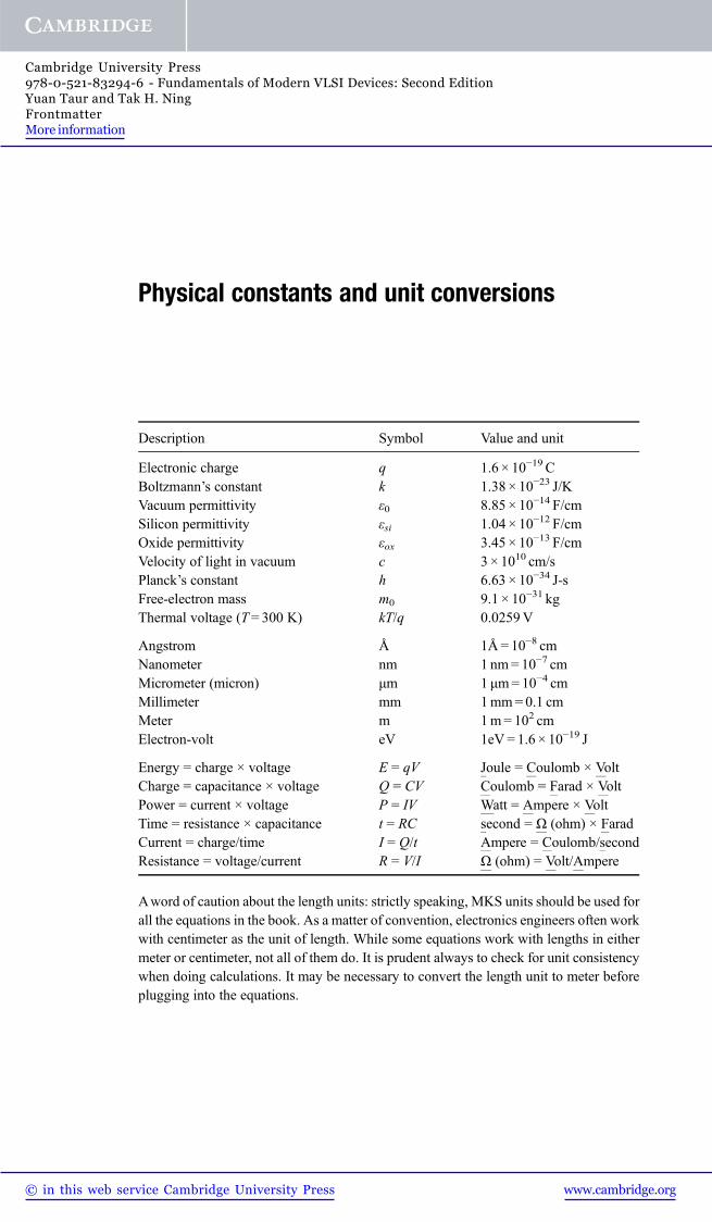
Physical constants and unit conversions
Description Symbol Value and unit
Electronic charge q 1.6 × 10⁻¹⁹ CBoltzmann’s constant k 1.38 × 10⁻²³ J/KVacuum permittivity ε0 8.85 × 10⁻¹⁴ F/cmSilicon permittivity εsi 1.04 × 10⁻¹² F/cmOxide permittivity εox 3.45 × 10⁻¹³ F/cmVelocity of light in vacuum c 3 × 1010 cm/sPlanck’s constant h 6.63 × 10⁻³⁴ J-sFree-electron mass m0 9.1 × 10⁻³¹ kgThermal voltage (T= 300 K) kT/q 0.0259V
Angstrom Å 1Å= 10−8 cmNanometer nm 1 nm= 10−7 cmMicrometer (micron) μm 1 μm=10−4 cmMillimeter mm 1mm=0.1 cmMeter m 1m= 102 cmElectron-volt eV 1eV= 1.6 × 10⁻¹⁹ J
Energy = charge × voltage E = qV Joule = Coulomb × VoltCharge = capacitance × voltage Q = CV Coulomb = Farad × VoltPower = current × voltage P = IV Watt = Ampere × VoltTime = resistance × capacitance t = RC second = Ω (ohm) × FaradCurrent = charge/time I = Q/t Ampere = Coulomb/secondResistance = voltage/current R = V/I Ω (ohm) = Volt/Ampere
Aword of caution about the length units: strictly speaking, MKS units should be used forall the equations in the book. As a matter of convention, electronics engineers often workwith centimeter as the unit of length. While some equations work with lengths in eithermeter or centimeter, not all of them do. It is prudent always to check for unit consistencywhen doing calculations. It may be necessary to convert the length unit to meter beforeplugging into the equations.
www.cambridge.org© in this web service Cambridge University Press
Cambridge University Press978-0-521-83294-6 - Fundamentals of Modern VLSI Devices: Second EditionYuan Taur and Tak H. NingFrontmatterMore information

List of symbols
Symbol Description Unit
A Area cm2
AE Emitter area cm2
α Common-base current gain Noneα0 Static common-base current gain NoneαF Forward common-base current gain in the Ebers–Moll model NoneαR Reverse common-base current gain in the Ebers–Moll model NoneαT Base transport factor Noneαn Electron-initiated rate of electron–hole pair generation per
unit distancecm−1
αp Hole-initiated rate of electron–hole pair generation per unitdistance
cm−1
BV Breakdown voltage VBVCBO Collector–base junction breakdown voltage with emitter
open circuitV
BVCEO Collector–emitter breakdown voltage with base open circuit VBVEBO Emitter–base junction breakdown voltage with collector
open circuitV
β Current gain Noneβ0 Static common-emitter current gain NoneβF Forward common-emitter current gain in the Ebers–Moll
modelNone
βR Reverse common-emitter current gain in the Ebers–Mollmodel
None
c Velocity of light in vacuum (= 3 × 1010 cm/s) cm/sC Capacitance FCd Depletion-layer capacitance per unit area F/cm2
Cd,tot Total depletion-layer capacitance FCdBC Base–collector diode depletion-layer capacitance per unit
areaF/cm2
CdBC,tot Total base–collector diode depletion-layer capacitance FCdBE Base–emitter diode depletion-layer capacitance per unit area F/cm2
CdBE,tot Total base–emitter diode depletion-layer capacitance FCdm Maximum depletion-layer capacitance (per unit area) F (F/cm2)CD Diffusion capacitance F
www.cambridge.org© in this web service Cambridge University Press
Cambridge University Press978-0-521-83294-6 - Fundamentals of Modern VLSI Devices: Second EditionYuan Taur and Tak H. NingFrontmatterMore information

CDn Diffusion capacitance due to excess electrons FCDp Diffusion capacitance due to excess holes FCDE Emitter diffusion capacitance FCDoS Equivalent density-of-states capacitance F/m2
Cfb MOS capacitance at flat band per unit area F/cm2
CFC Capacitance between the floating gate and the control gate ofa MOSFET nonvolatile memory device
F
Cg Intrinsic gate capacitance per unit area F/cm2
CG Total gate capacitance of MOSFET FCi Inversion-layer capacitance per unit area F/cm2
Cit Interface trap capacitance per unit area F/cm2
Cj Junction capacitance per unit area F/cm2
CJ Junction capacitance FCL Load capacitance FCin Equivalent input capacitance of a logic gate FCinv MOSFET capacitance in inversion per unit area F/cm2
Cmin Minimum MOS capacitance per unit area F/cm2
Cout Equivalent output capacitance of a logic gate FCov Gate-to-source (-drain) overlap capacitance (per edge) FCox Oxide capacitance per unit area F/cm2
Cp Polysilicon-gate depletion-layer capacitance per unit area F/cm2
Csi Silicon capacitance per unit area F/cm2
Cw Wire capacitance per unit length F/cmCπ Base–emitter capacitance in the small-signal hybrid-π
equivalent-circuit modelF
Cμ Base–collector capacitance in the small-signal hybrid-πequivalent-circuit model
F
d Width of diffusion region in a MOSFET cmDn Electron diffusion coefficient cm2/sDnB Electron diffusion coefficient in the base of an n–p–n transistor cm2/sDp Hole diffusion coefficient cm2/sDpE Hole diffusion coefficient in the emitter of an n–p–n transistor cm2/sΔVt Threshold voltage rolloff due to short-channel effect VΔEg Apparent bandgap narrowing JΔEgB Bandgap-narrowing parameter in the base region JΔEg,max Maximum bandgap narrowing due to the presence of Ge JΔEg,SiGe Local bandgap narrowing due to the presence of Ge JΔL Channel length modulation in MOSFET cmΔQtotal Total charge stored in a nonvolatile memory device CE Energy JEc Conduction-band edge JEv Valence-band edge JEa Ionized-acceptor energy level J
List of symbols xvii
www.cambridge.org© in this web service Cambridge University Press
Cambridge University Press978-0-521-83294-6 - Fundamentals of Modern VLSI Devices: Second EditionYuan Taur and Tak H. NingFrontmatterMore information
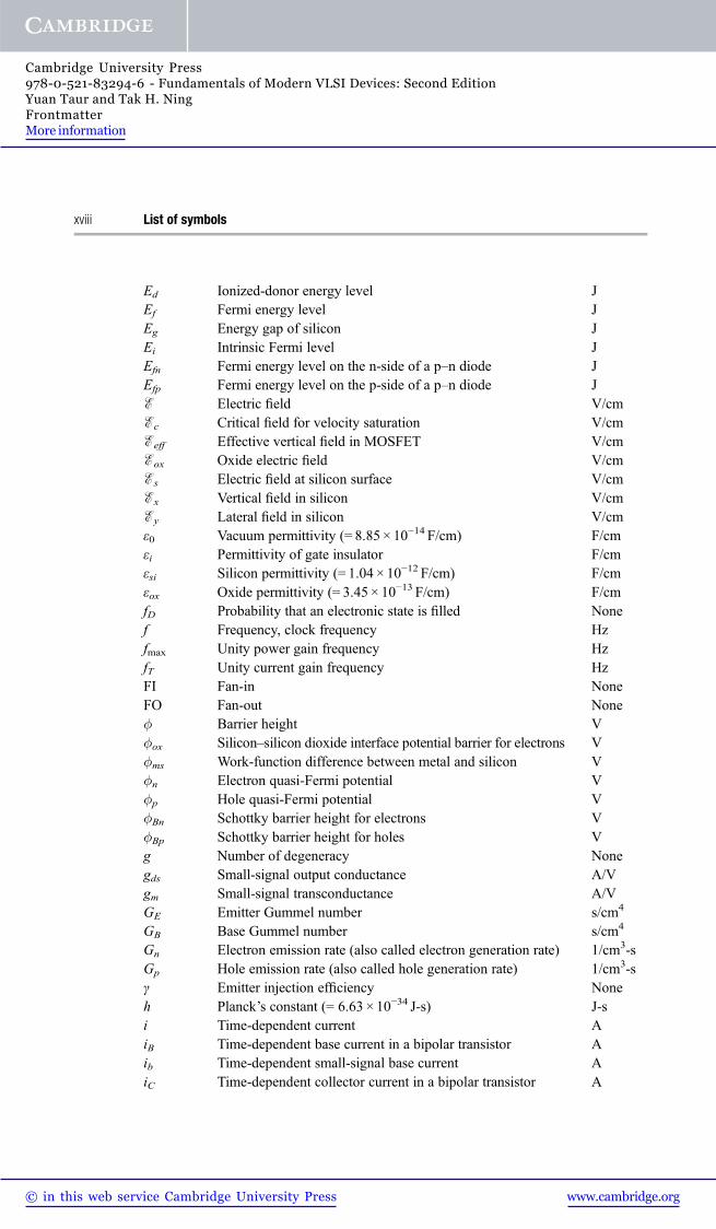
Ed Ionized-donor energy level JEf Fermi energy level JEg Energy gap of silicon JEi Intrinsic Fermi level JEfn Fermi energy level on the n-side of a p–n diode JEfp Fermi energy level on the p-side of a p–n diode JE Electric field V/cmE c Critical field for velocity saturation V/cmE eff Effective vertical field in MOSFET V/cmE ox Oxide electric field V/cmE s Electric field at silicon surface V/cmE x Vertical field in silicon V/cmE y Lateral field in silicon V/cmε0 Vacuum permittivity (= 8.85 × 10⁻¹⁴ F/cm) F/cmεi Permittivity of gate insulator F/cmεsi Silicon permittivity (= 1.04 × 10⁻¹² F/cm) F/cmεox Oxide permittivity (= 3.45 × 10⁻¹³ F/cm) F/cmfD Probability that an electronic state is filled Nonef Frequency, clock frequency Hzfmax Unity power gain frequency HzfT Unity current gain frequency HzFI Fan-in NoneFO Fan-out None� Barrier height V�ox Silicon–silicon dioxide interface potential barrier for electrons V�ms Work-function difference between metal and silicon V�n Electron quasi-Fermi potential V�p Hole quasi-Fermi potential V�Bn Schottky barrier height for electrons V�Bp Schottky barrier height for holes Vg Number of degeneracy Nonegds Small-signal output conductance A/Vgm Small-signal transconductance A/VGE Emitter Gummel number s/cm4
GB Base Gummel number s/cm4
Gn Electron emission rate (also called electron generation rate) 1/cm3-sGp Hole emission rate (also called hole generation rate) 1/cm3-sγ Emitter injection efficiency Noneh Planck’s constant (= 6.63 × 10⁻³⁴ J-s) J-si Time-dependent current AiB Time-dependent base current in a bipolar transistor Aib Time-dependent small-signal base current AiC Time-dependent collector current in a bipolar transistor A
xviii List of symbols
www.cambridge.org© in this web service Cambridge University Press
Cambridge University Press978-0-521-83294-6 - Fundamentals of Modern VLSI Devices: Second EditionYuan Taur and Tak H. NingFrontmatterMore information
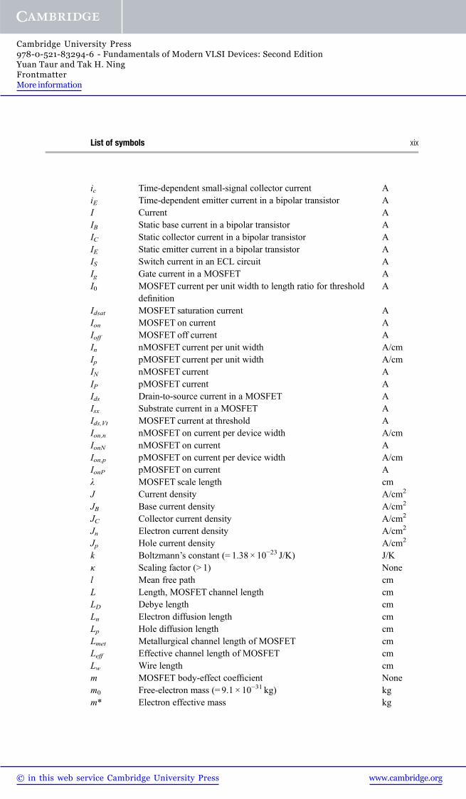
ic Time-dependent small-signal collector current AiE Time-dependent emitter current in a bipolar transistor AI Current AIB Static base current in a bipolar transistor AIC Static collector current in a bipolar transistor AIE Static emitter current in a bipolar transistor AIS Switch current in an ECL circuit AIg Gate current in a MOSFET AI0 MOSFET current per unit width to length ratio for threshold
definitionA
Idsat MOSFET saturation current AIon MOSFET on current AIoff MOSFET off current AIn nMOSFET current per unit width A/cmIp pMOSFET current per unit width A/cmIN nMOSFET current AIP pMOSFET current AIds Drain-to-source current in a MOSFET AIsx Substrate current in a MOSFET AIds,Vt MOSFET current at threshold AIon,n nMOSFET on current per device width A/cmIonN nMOSFET on current AIon,p pMOSFET on current per device width A/cmIonP pMOSFET on current Aλ MOSFET scale length cmJ Current density A/cm2
JB Base current density A/cm2
JC Collector current density A/cm2
Jn Electron current density A/cm2
Jp Hole current density A/cm2
k Boltzmann’s constant (= 1.38 × 10⁻²³ J/K) J/Kκ Scaling factor (> 1) Nonel Mean free path cmL Length, MOSFET channel length cmLD Debye length cmLn Electron diffusion length cmLp Hole diffusion length cmLmet Metallurgical channel length of MOSFET cmLeff Effective channel length of MOSFET cmLw Wire length cmm MOSFET body-effect coefficient Nonem0 Free-electron mass (= 9.1 × 10⁻³¹ kg) kgm* Electron effective mass kg
List of symbols xix
www.cambridge.org© in this web service Cambridge University Press
Cambridge University Press978-0-521-83294-6 - Fundamentals of Modern VLSI Devices: Second EditionYuan Taur and Tak H. NingFrontmatterMore information
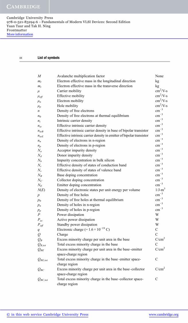
M Avalanche multiplication factor Noneml Electron effective mass in the longitudinal direction kgmt Electron effective mass in the transverse direction kgμ Carrier mobility cm2/V-sμeff Effective mobility cm2/V-sμn Electron mobility cm2/V-sμp Hole mobility cm2/V-sn Density of free electrons cm−3
n0 Density of free electrons at thermal equilibrium cm−3
ni Intrinsic carrier density cm−3
nie Effective intrinsic carrier density cm−3
nieB Effective intrinsic carrier density in base of bipolar transistor cm−3
nieE Effective intrinsic carrier density in emitter of bipolar transistor cm−3
nn Density of electrons in n-region cm−3
np Density of electrons in p-region cm−3
Na Acceptor impurity density cm−3
Nd Donor impurity density cm−3
Nb Impurity concentration in bulk silicon cm−3
Nc Effective density of states of conduction band cm−3
Nv Effective density of states of valence band cm−3
NB Base doping concentration cm−3
NC Collector doping concentration cm−3
NE Emitter doping concentration cm−3
N(E) Density of electronic states per unit energy per volume 1/J-m3
p Density of free holes cm−3
p0 Density of free holes at thermal equilibrium cm−3
pn Density of holes in n-region cm−3
pp Density of holes in p-region cm−3
P Power dissipation WPac Active power dissipation WPoff Standby power dissipation Wq Electronic charge (= 1.6 × 10⁻¹⁹ C) CQ Charge CQB Excess minority charge per unit area in the base C/cm2
QB,tot Total excess minority charge in the base CQBE Excess minority charge per unit area in the base–emitter
space-charge regionC/cm2
QBE,tot Total excess minority charge in the base–emitter space-charge region
C
QBC Excess minority charge per unit area in the base–collectorspace-charge region
C/cm2
QBC,tot Total excess minority charge in the base–collector space-charge region
C
xx List of symbols
www.cambridge.org© in this web service Cambridge University Press
Cambridge University Press978-0-521-83294-6 - Fundamentals of Modern VLSI Devices: Second EditionYuan Taur and Tak H. NingFrontmatterMore information
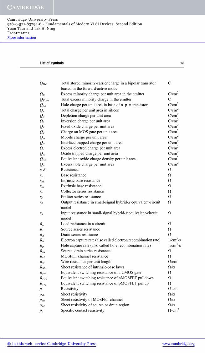
QDE Total stored minority-carrier charge in a bipolar transistorbiased in the forward-active mode
C
QE Excess minority charge per unit area in the emitter C/cm2
QE,tot Total excess minority charge in the emitter CQpB Hole charge per unit area in base of n–p–n transistor C/cm2
Qs Total charge per unit area in silicon C/cm2
Qd Depletion charge per unit area C/cm2
Qi Inversion charge per unit area C/cm2
Qf Fixed oxide charge per unit area C/cm2
Qg Charge on MOS gate per unit area C/cm2
Qm Mobile charge per unit area C/cm2
Qit Interface trapped charge per unit area C/cm2
Qn Excess electron charge per unit area C/cm2
Qot Oxide trapped charge per unit area C/cm2
Qox Equivalent oxide charge density per unit area C/cm2
Qp Excess hole charge per unit area C/cm2
r, R Resistance Ωrb Base resistance Ωrbi Intrinsic base resistance Ωrbx Extrinsic base resistance Ωrc Collector series resistance Ωre Emitter series resistance Ωr0 Output resistance in small-signal hybrid-π equivalent-circuit
modelΩ
rπ Input resistance in small-signal hybrid-π equivalent-circuitmodel
Ω
RL Load resistance in a circuit ΩRs Source series resistance ΩRd Drain series resistance ΩRn Electron capture rate (also called electron recombination rate) 1/cm3-sRp Hole capture rate (also called hole recombination rate) 1/cm3-sRsd Source–drain series resistance ΩRch MOSFET channel resistance ΩRw Wire resistance per unit length Ω/cmRSbi Sheet resistance of intrinsic-base layer Ω/□Rsw Equivalent switching resistance of a CMOS gate ΩRswn Equivalent switching resistance of nMOSFET pulldown ΩRswp Equivalent switching resistance of pMOSFET pullup Ωρ Resistivity Ω-cmρsh Sheet resistivity Ω/□ρch Sheet resistivity of MOSFET channel Ω/□ρsd Sheet resistivity of source or drain region Ω/□ρc Specific contact resistivity Ω-cm2
List of symbols xxi
www.cambridge.org© in this web service Cambridge University Press
Cambridge University Press978-0-521-83294-6 - Fundamentals of Modern VLSI Devices: Second EditionYuan Taur and Tak H. NingFrontmatterMore information

ρnet Volume density of net charge C/cm3
S MOSFET inverse subthreshold current slope V/decadeSp Surface recombination velocity for holes cm/sσL Lateral straggle of Gaussian doping profile cmt Time stB Base transit time stE Emitter transit time stBE Base–emitter depletion-layer transit time stBC Base–collector depletion-layer transit time sti Thickness of gate insulator cmtinv Equivalent oxide thickness for inversion charge calculations cmtox Oxide thickness cmtr Transit time stw Thickness of wire cmtsi Thickness of silicon film cmT Absolute temperature Kτ Lifetime sτ Circuit delay sτb Buffered delay sτint Intrinsic, unloaded delay sτF Forward transit time of bipolar transistor sτn Electron lifetime sτn nMOSFET pulldown delay sτnB Electron lifetime in base of n–p–n transistor sτp Hole lifetime sτp pMOSFET pullup delay sτpE Hole lifetime in emitter of n–p–n transistor sτR Reverse transit time of bipolar transistor sτw Wire RC delay sτE Emitter delay time sτB Base delay time sτBE Base–emitter depletion-region delay time sτBC Base–collector depletion-region delay time sU Net recombination rate 1/cm3-sν Velocity cm/sv Small-signal voltage Vνth Thermal velocity cm/sνd Carrier drift velocity cm/sνsat Saturation velocity of carriers cm/svT Thermal injection velocity at MOSFET source cm/sV Voltage VV Quasi-Fermi potential along MOSFET channel VVA Early voltage V
xxii List of symbols
www.cambridge.org© in this web service Cambridge University Press
Cambridge University Press978-0-521-83294-6 - Fundamentals of Modern VLSI Devices: Second EditionYuan Taur and Tak H. NingFrontmatterMore information
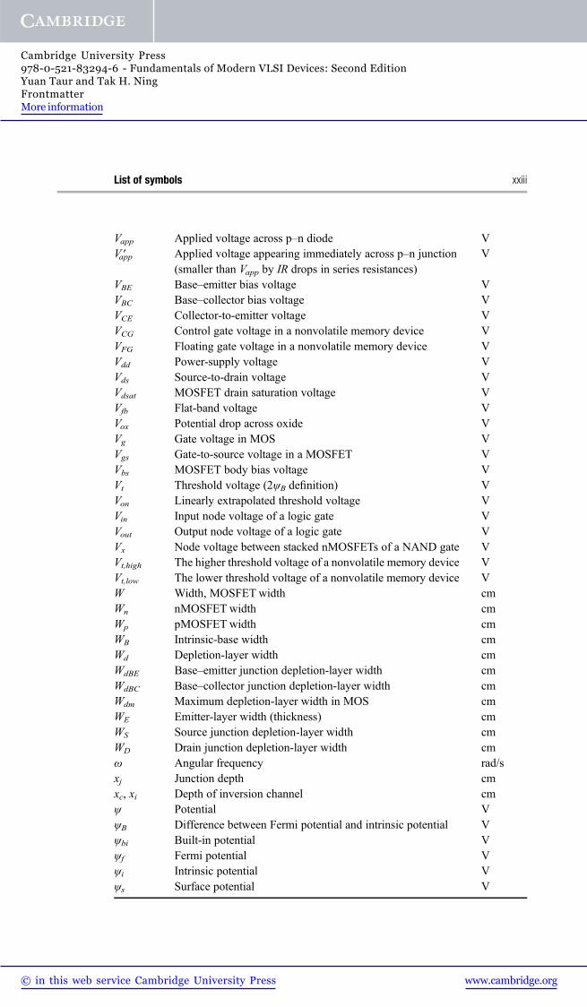
Vapp Applied voltage across p–n diode VV ′app Applied voltage appearing immediately across p–n junction
(smaller than Vapp by IR drops in series resistances)V
VBE Base–emitter bias voltage VVBC Base–collector bias voltage VVCE Collector-to-emitter voltage VVCG Control gate voltage in a nonvolatile memory device VVFG Floating gate voltage in a nonvolatile memory device VVdd Power-supply voltage VVds Source-to-drain voltage VVdsat MOSFET drain saturation voltage VVfb Flat-band voltage VVox Potential drop across oxide VVg Gate voltage in MOS VVgs Gate-to-source voltage in a MOSFET VVbs MOSFET body bias voltage VVt Threshold voltage (2ψB definition) VVon Linearly extrapolated threshold voltage VVin Input node voltage of a logic gate VVout Output node voltage of a logic gate VVx Node voltage between stacked nMOSFETs of a NAND gate VVt,high The higher threshold voltage of a nonvolatile memory device VVt,low The lower threshold voltage of a nonvolatile memory device VW Width, MOSFET width cmWn nMOSFET width cmWp pMOSFET width cmWB Intrinsic-base width cmWd Depletion-layer width cmWdBE Base–emitter junction depletion-layer width cmWdBC Base–collector junction depletion-layer width cmWdm Maximum depletion-layer width in MOS cmWE Emitter-layer width (thickness) cmWS Source junction depletion-layer width cmWD Drain junction depletion-layer width cmω Angular frequency rad/sxj Junction depth cmxc, xi Depth of inversion channel cmψ Potential VψB Difference between Fermi potential and intrinsic potential Vψbi Built-in potential Vψf Fermi potential Vψi Intrinsic potential Vψs Surface potential V
List of symbols xxiii
www.cambridge.org© in this web service Cambridge University Press
Cambridge University Press978-0-521-83294-6 - Fundamentals of Modern VLSI Devices: Second EditionYuan Taur and Tak H. NingFrontmatterMore information


![Ece-V-fundamentals of Cmos Vlsi [10ec56]-Solution](https://static.fdocuments.in/doc/165x107/55cf9d28550346d033ac77f4/ece-v-fundamentals-of-cmos-vlsi-10ec56-solution.jpg)