
Full color led display research based on chip on board(COB) package
22
-
Upload
keshav-kumar -
Category
Engineering
-
view
34 -
download
0
Transcript of Full color led display research based on chip on board(COB) package


Full-color LED displayresearch based onchip on board(COB)
package
Presented By:- KESHAV KUMAR
S7, ECE
Roll No.- 53
Guided By:- Mr. Nishanth Sir

CONTENTS KEYWORDS
INTRODUCTIONI. SCREEN
II. RGB
RESEARCHING PROCESSI. PACKAGING
II. PLASTIC PACKAGE METHOD
III. EXISTING SMD
IV. COB PACKAGE
V. LED CHIPS
VI. BONDING
VII. MICROGRAPH
VIII. VISUAL EFFECT
ADVANTAGE
CONCLUSION
REFERENCES
Keywords Chip on board(COB)- an integrated package
method which encapsulate LED chip onto the substrate directly.
LED display- An LED display is a flat panel display, which uses an array of light-emitting diodes as pixels for a video display.
SMD(surface mounted device)- a method for producing electronic circuits in which the components are mounted or placed directly onto the surface of printed circuit boards called a surface-mount device (SMD)
Die bond- Place enlarge crystal ring with silver glue in crystal picking frame, then pick the LED chip onto the printed circuit board.
Wire bond- Solder LED chip onto homologous pad of printed circuit board with wire bonder.
INTRODUCTION
LED display was sorted by color-
1. Monochrome screen
2. Double color screen
3. Full color screen Sorted by application place-
1. Outdoor screen
2. Indoor screen Sorted by control mode-
1. Synchronous control panel
2. Asynchronous control panel

SCREEN
Outdoor Screen
Indoor Screen

Sensitivity of human eyes, ability to distinguish different colors from three different types of retinal cones.
One of three kinds of cones is sensitive to red(R), green(G) or blue(B).
When the light source disappeared, there is a delay time called human visual inertia, it formed driving method called dynamic scanning driving.
RGB

RESEARCHING PROCESS
COB package process of LED display modules include following steps:-
1. Die spreading
2. Fluid dispensing
3. Die bonding
4. Constant temperature backing
5. Wire bonding
6. Former test
7. Whole board molding
8. Solidification
9. Back test
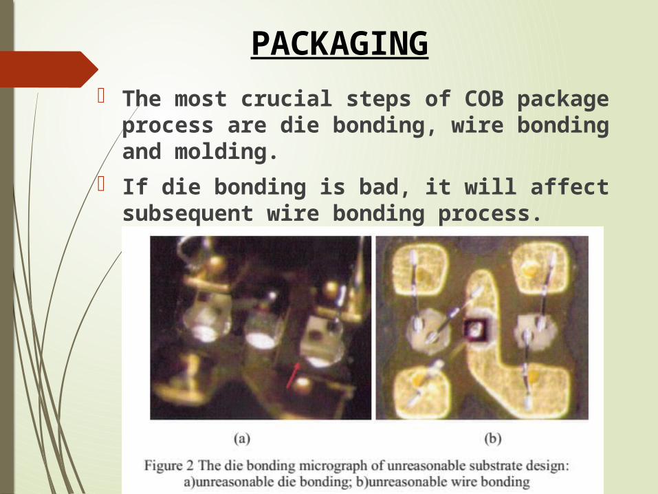
The most crucial steps of COB package process are die bonding, wire bonding and molding.
If die bonding is bad, it will affect subsequent wire bonding process.
PACKAGING

After die bonding, wire bonding and electronic tested to be correct, plastic package should be done.
Due to this consistency is better and it has a better effect of display and high reliability.
PLASTIC PACKAGE METHOD

Existing P2.0 LED display mainly uses surface mount SMD packages lamp to assemble onto the substrate of the LED display module by reflow soldering.
In which SMD, a red, a green and a blue chip is packaged, the anode of the tri-color chips are connected to adapt the dynamic scanning driving of existing LED display.
EXISTING SMD
COB package of the P2.0 LED display module, which uses the 1/32 dynamic scanning driving method.
The module has a resolution of 32 * 32 and contains a total of 32 * 32 * 3 LED chips used to display.
The entire scanning driver circuit can be divided into four modules:-
1.External IO module
2.the row scanning module
3.the column driving module
4.LED array module.
COB PACKAGE


The red, green and blue LED chips was chosen to package the COB display module with the pixel pitch of 2.0mm.
Among them, the red LED chip has counter electrode vertical structure, that is to say the bottom surface of the chip is its anode and its cathode is on the top surface; the blue and green chip has a horizontal structure which has a sapphire substrate and on the top surface of which are its anode and cathode.
LED CHIPS
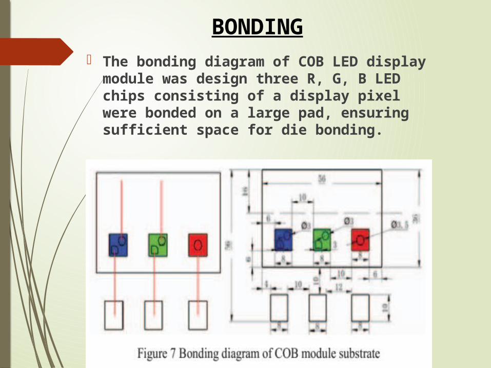
The bonding diagram of COB LED display module was design three R, G, B LED chips consisting of a display pixel were bonded on a large pad, ensuring sufficient space for die bonding.
BONDING
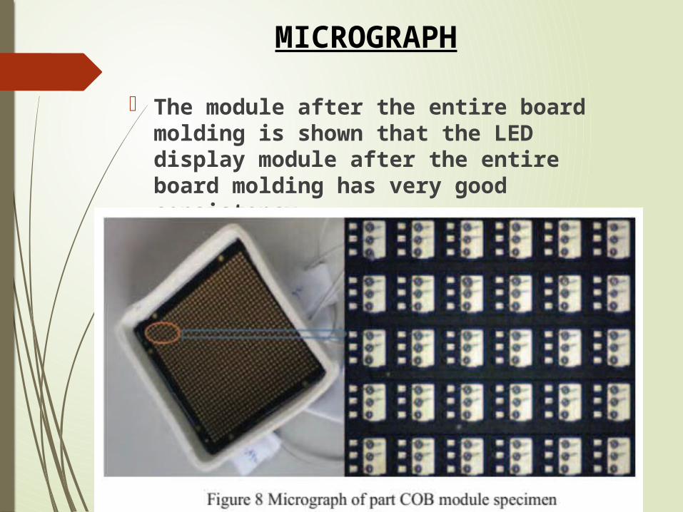
The module after the entire board molding is shown that the LED display module after the entire board molding has very good consistency.
MICROGRAPH
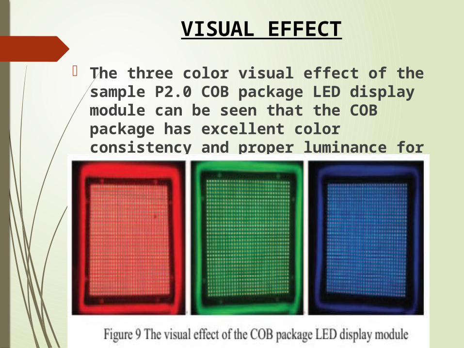
The three color visual effect of the sample P2.0 COB package LED display module can be seen that the COB package has excellent color consistency and proper luminance for display requirement.
VISUAL EFFECT

ADVANTAGE
COB package has the features as simple processes
Low cost Good visual effect High reliability Long life-span, etc. While SMD 3 in 1 package has many
defects, for instance, high cost, complicated processes, lamps can easily go dead and be knocked off, etc.
COB can be a very good solution for package of high definition LED display.
CONCLUSION The sort of the LED dies, controlling in the yield of die
bonding and wire bonding and precision in molding packaging.
Before COB package, LED chip has to be carefully tested and sorted to guarantee the brightness and chrominance.
When designing the module substrate, enough space should be offered for die bond and soldering plate of the wire, to ensure the glue cover on four sides and form strong connection.
Wire bonding direction and distance should be designed as almost the same, this is to decrease the difficulty of soldering operation.
For molding packaging on the whole board, every module should under protection with plastic packaging and also need same packaging thickness.
REFERENCES
Shih-Mim Liu, Ching-Feng Chen and Kuang-Chung Chou.” The design and implementation of a low-cost 360-degree color LED display system”[C].0098 3063/11/2011 IEEE:289-295.
K.Takahashi , S.Nakajima and S.Takeuchi. “Full .color LED display panel fabricated on a silicon microreflector “[C]. 0-7803-3744-1/97/ IEEE 356-359.
Joon Ho Hyun, Myung Jin Park, and Young Hwan Kim. “POSCO LED and the IT Consilience Creative Program of MKE and NIPA,2012”[C]978-1-4673-0219-7/122012 IEEE
https://en.wikipedia.org/wiki/Color

THANK YOU


![CITILED COB+ Series · Ref.CE-P2987 02/15 [5] 1. Introduction 1-1. Product Description G 1-2. Features COB+ is the new type of LED package AC-Driver embedded in the standard COB(Chip](https://static.fdocuments.in/doc/165x107/60ccff13a6b2a15cd151099d/citiled-cob-series-refce-p2987-0215-5-1-introduction-1-1-product-description.jpg)
