Freescale Semiconductor Document Number: … · The 33982 is a self-protected silicon 2.0 mO hm...
37
* This document contains certain information on a new product. Specifications and information herein are subject to change without notice. Document Number: MC33982 Rev. 18.0, 9/2014 Freescale Semiconductor Advance Information © Freescale Semiconductor, Inc., 2007-2014. All rights reserved. Single Intelligent High-current Self- protected High-side Switch (2.0 mOhm) The 33982 is a self-protected silicon 2.0 mOhm high-side switch used to replace electromechanical relays, fuses, and discrete devices in power management applications. The 33982 is designed for harsh environments and includes self- recovery features. The device is suitable for loads with high inrush current, as well as motors and all types of resistive and inductive loads. Programming, control, and diagnostics are implemented via the serial peripheral interface (SPI). A dedicated parallel input is available for alternate and pulse- width modulation (PWM) control of the output. SPI-programmable fault trip thresholds allow the device to be adjusted for optimal performance in the application. Features • Single 2.0 m max high-side switch with parallel input or SPI control • 6.0 V to 27 V operating voltage with standby currents < 5.0 A • Output current monitoring with two SPI-selectable current ratios • SPI control of overcurrent limit, overcurrent fault blanking time, output OFF open load detection, output ON/OFF control, watchdog timeout, slew rates, and fault status reporting • SPI status reporting of overcurrent, open and shorted loads, overtemperature shutdown, undervoltage and overvoltage shutdown, Fail-safe pin status, and program status • Enhanced -16 V reverse polarity V PWR protection Figure 1. 33982 Simplified Application Diagram HIGH-SIDE SWITCH 33982 Applications • DC motor or solenoid • Resistive and inductive loads • Low-voltage lighting SCALE 1:1 Bottom View FK SUFFIX 98ARL10521D 16-PIN PQFN VDD I/O I/O SO SCLK CS SI I/O I/O A/D VPWR FS WAKE SI SCLK CS SO RST IN CSNS FSI GND HS GND LOAD 33982 MCU V DD V DD V DD V PWR GND PWR GND
Transcript of Freescale Semiconductor Document Number: … · The 33982 is a self-protected silicon 2.0 mO hm...

Document Number: MC33982Rev. 18.0, 9/2014
Freescale SemiconductorAdvance Information
Single Intelligent High-current Self-protected High-side Switch (2.0 mOhm)The 33982 is a self-protected silicon 2.0 mOhm high-side switch used to replace electromechanical relays, fuses, and discrete devices in power management applications. The 33982 is designed for harsh environments and includes self-recovery features. The device is suitable for loads with high inrush current, as well as motors and all types of resistive and inductive loads.Programming, control, and diagnostics are implemented via the serial peripheral interface (SPI). A dedicated parallel input is available for alternate and pulse-width modulation (PWM) control of the output. SPI-programmable fault trip thresholds allow the device to be adjusted for optimal performance in the application.
Features
• Single 2.0 m max high-side switch with parallel input or SPI control • 6.0 V to 27 V operating voltage with standby currents < 5.0 A• Output current monitoring with two SPI-selectable current ratios• SPI control of overcurrent limit, overcurrent fault blanking time, output OFF
open load detection, output ON/OFF control, watchdog timeout, slew rates, and fault status reporting
• SPI status reporting of overcurrent, open and shorted loads, overtemperature shutdown, undervoltage and overvoltage shutdown, Fail-safe pin status, and program status
• Enhanced -16 V reverse polarity VPWR protection
Figure 1. 33982 Simplified Application Diagram
HIGH-SIDE SWITCH
33982
Applications
• DC motor or solenoid• Resistive and inductive loads• Low-voltage lighting
SCALE 1:1
Bottom View
FK SUFFIX98ARL10521D16-PIN PQFN
VDD
I/O
I/O
SO
SCLK
CS
SI
I/O
I/O
A/D
VPWR
FS
WAKE
SI
SCLK
CS
SO
RST
IN
CSNS
FSI GND
HS
GND
LOAD
33982
MCU
VDDVDDVDD VPWR
GND PWR GND
* This document contains certain information on a new product.Specifications and information herein are subject to change without notice.
© Freescale Semiconductor, Inc., 2007-2014. All rights reserved.

ORDERABLE PARTS
ORDERABLE PARTS
Table 1. Orderable Part Variations (1)
Part Number Temperature (TA) PackageOutput Clamp
EnergyReference Location
OD3 bit for X111 address
Reference Location
MC33982CHFK -40 °C to 125 °C 16 PQFN 1.0J Table 3 1 Table 16
Notes1. To order parts in Tape & Reel, add the R2 suffix to the part number.
Analog Integrated Circuit Device Data2 Freescale Semiconductor
33982
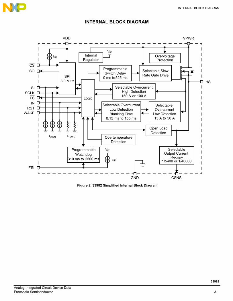
INTERNAL BLOCK DIAGRAM
INTERNAL BLOCK DIAGRAM
Figure 2. 33982 Simplified Internal Block Diagram
GND
ProgrammableWatchdog
310 ms to 2500 ms
OvertemperatureDetection
SelectableOutput Current
Recopy1/5400 or 1/40000
Open LoadDetection
Logic
SPI3.0 MHz
Selectable OvercurrentLow Detection
0.15 ms to 155 ms
Selectable
Low Detection15 A to 50 A
Selectable OvercurrentHigh Detection150 A or 100 A
InternalRegulator
ProgrammableSwitch Delay
0 ms to525 ms
Selectable SlewRate Gate Drive
OvervoltageProtection
HS
CSNS
VPWRVDD
CS
SO
SISCLK
FS
INRST
WAKE
FSI
VIC
VIC
IDWN RDWN
IUP
IUP
Blanking TimeOvercurrent
Analog Integrated Circuit Device DataFreescale Semiconductor 3
33982
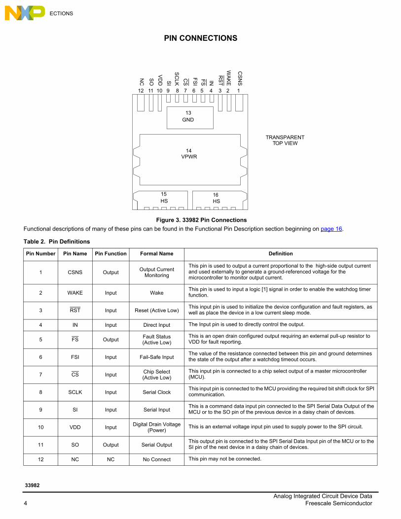
PIN CONNECTIONS
PIN CONNECTIONS
Figure 3. 33982 Pin Connections
Functional descriptions of many of these pins can be found in the Functional Pin Description section beginning on page 16.
Table 2. Pin Definitions
Pin Number Pin Name Pin Function Formal Name Definition
1 CSNS OutputOutput Current
Monitoring
This pin is used to output a current proportional to the high-side output current and used externally to generate a ground-referenced voltage for the microcontroller to monitor output current.
2 WAKE Input WakeThis pin is used to input a logic [1] signal in order to enable the watchdog timer function.
3 RST Input Reset (Active Low)This input pin is used to initialize the device configuration and fault registers, as well as place the device in a low current sleep mode.
4 IN Input Direct Input The Input pin is used to directly control the output.
5 FS OutputFault Status(Active Low)
This is an open drain configured output requiring an external pull-up resistor to VDD for fault reporting.
6 FSI Input Fail-Safe InputThe value of the resistance connected between this pin and ground determines the state of the output after a watchdog timeout occurs.
7 CS InputChip Select(Active Low)
This input pin is connected to a chip select output of a master microcontroller (MCU).
8 SCLK Input Serial ClockThis input pin is connected to the MCU providing the required bit shift clock for SPI communication.
9 SI Input Serial InputThis is a command data input pin connected to the SPI Serial Data Output of the MCU or to the SO pin of the previous device in a daisy chain of devices.
10 VDD InputDigital Drain Voltage
(Power)This is an external voltage input pin used to supply power to the SPI circuit.
11 SO Output Serial OutputThis output pin is connected to the SPI Serial Data Input pin of the MCU or to the SI pin of the next device in a daisy chain of devices.
12 NC NC No Connect This pin may not be connected.
HS HS1615
VPWR14
GND13
CS
NSINFS
FS
I
CS
SC
LK
RS
T
WA
KESI
VD
D
SO
NC
111 10 9 8 7 6 5 4 3 212
TRANSPARENTTOP VIEW
Analog Integrated Circuit Device Data4 Freescale Semiconductor
33982

PIN CONNECTIONS
13 GND Ground Ground This pin is the ground for the logic and analog circuitry of the device.
14 VPWR InputPositive Power
SupplyThis pin connects to the positive power supply and is the source input of operational power for the device.
15, 16 HS Output High-side OutputProtected high-side power output to the load. Output pins must be connected in parallel for operation.
Table 2. Pin Definitions (continued)
Pin Number Pin Name Pin Function Formal Name Definition
Analog Integrated Circuit Device DataFreescale Semiconductor 5
33982

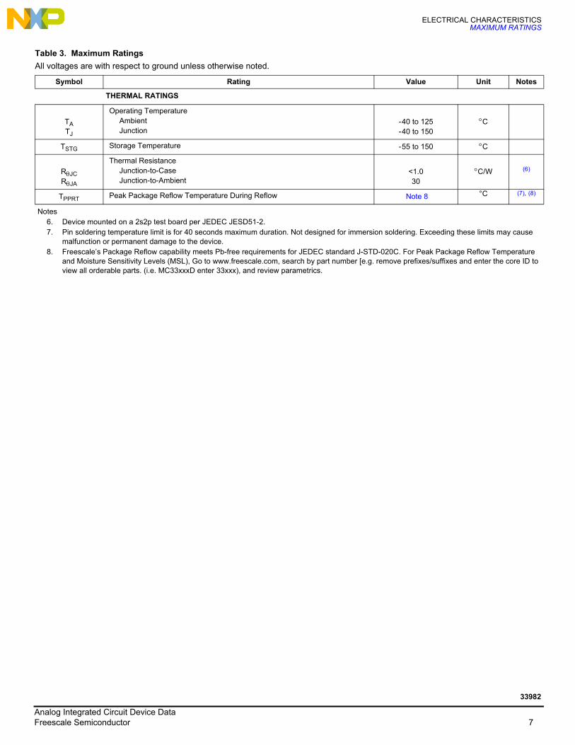
ELECTRICAL CHARACTERISTICSMAXIMUM RATINGS
ELECTRICAL CHARACTERISTICS
MAXIMUM RATINGS
Table 3. Maximum Ratings
All voltages are with respect to ground unless otherwise noted.
Symbol Rating Value Unit Notes
ELECTRICAL RATINGS
VPWROperating Voltage Range
Steady-state -16 to 41 V
VDD VDD Supply Voltage -0.3 to 5.5 V
VIN, RST, FSI, CSNS, SI, SCLK,
CS, FSInput/Output Voltage - 0.3 to 7.0 V (2)
VSO SO Output Voltage - 0.3 to VDD + 0.3 V (2)
ICL(WAKE) WAKE Input Clamp Current 2.5 mA
ICL(CSNS) CSNS Input Clamp Current 10 mA
IHS Output Current 60 A (3)
VHS
Output VoltagePositiveNegative
41 -15
V
ECL
Output Clamp Energy33982B33982C
1.51.0
J (4)
VESD1VESD3
ESD VoltageHuman Body Model (HBM)Charge Device Model (CDM)
Corner Pins (1, 12, 15, 16) All Other Pins (2, 11, 13, 14)
± 2000
±750±500
V (5)
Notes2. Exceeding this voltage limit may cause permanent damage to the device.3. Continuous high-side output current rating so long as maximum junction temperature is not exceeded. Calculation of maximum output current
using package thermal resistance is required. 4. Active clamp energy using single-pulse method (L = 16 mH, RL = 0, VPWR = 12 V, TJ = 150°C).
5. ESD1 testing is performed in accordance with the Human Body Model (HBM) (CZAP = 100 pF, RZAP = 1500 ESD3 testing is performed in
accordance with the Charge Device Model (CDM), Robotic (Czap = 4.0 pF).
Analog Integrated Circuit Device Data6 Freescale Semiconductor
33982
ELECTRICAL CHARACTERISTICSMAXIMUM RATINGS
THERMAL RATINGS
TATJ
Operating TemperatureAmbientJunction
- 40 to 125- 40 to 150
C
TSTG Storage Temperature - 55 to 150 C
RJCRJA
Thermal ResistanceJunction-to-CaseJunction-to-Ambient
<1.030
C/W (6)
TPPRT Peak Package Reflow Temperature During Reflow Note 8 °C (7), (8)
Notes6. Device mounted on a 2s2p test board per JEDEC JESD51-2.7. Pin soldering temperature limit is for 40 seconds maximum duration. Not designed for immersion soldering. Exceeding these limits may cause
malfunction or permanent damage to the device.8. Freescale’s Package Reflow capability meets Pb-free requirements for JEDEC standard J-STD-020C. For Peak Package Reflow Temperature
and Moisture Sensitivity Levels (MSL), Go to www.freescale.com, search by part number [e.g. remove prefixes/suffixes and enter the core ID to view all orderable parts. (i.e. MC33xxxD enter 33xxx), and review parametrics.
Table 3. Maximum Ratings
All voltages are with respect to ground unless otherwise noted.
Symbol Rating Value Unit Notes
Analog Integrated Circuit Device DataFreescale Semiconductor 7
33982
ELECTRICAL CHARACTERISTICSSTATIC ELECTRICAL CHARACTERISTICS
STATIC ELECTRICAL CHARACTERISTICS
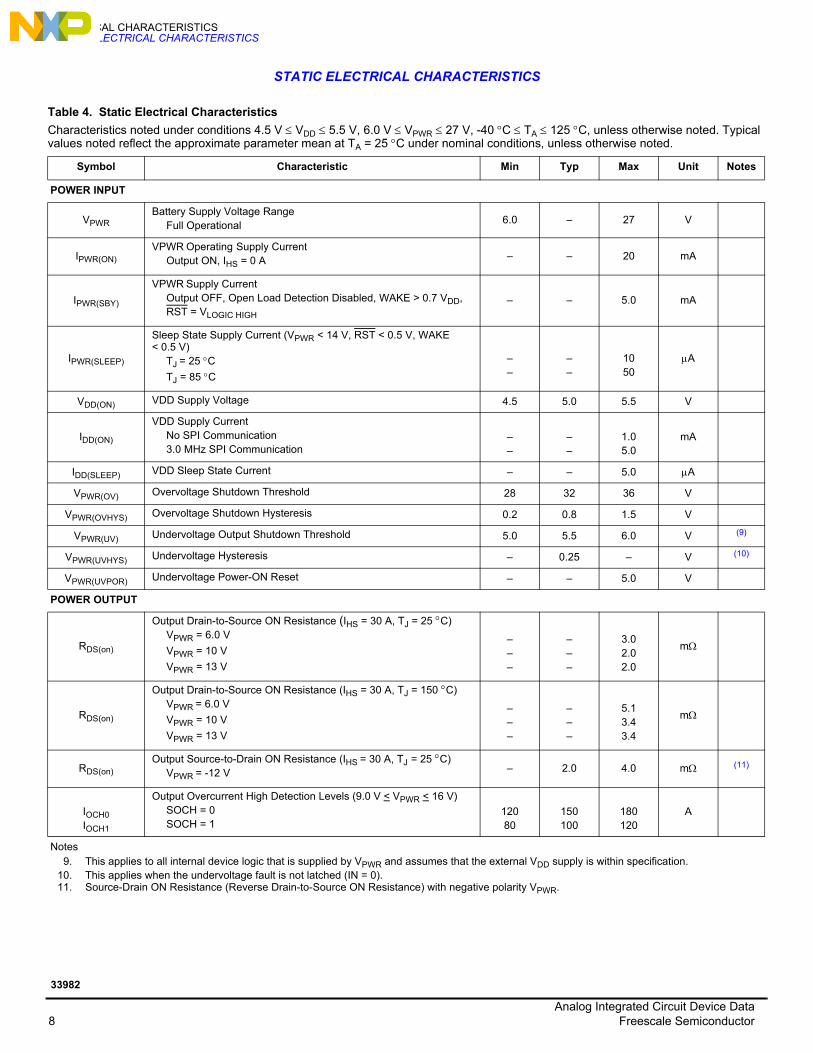
Table 4. Static Electrical Characteristics
Characteristics noted under conditions 4.5 V VDD 5.5 V, 6.0 V VPWR 27 V, -40 C TA 125 C, unless otherwise noted. Typical values noted reflect the approximate parameter mean at TA = 25 C under nominal conditions, unless otherwise noted.
Symbol Characteristic Min Typ Max Unit Notes
POWER INPUT
VPWRBattery Supply Voltage Range
Full Operational 6.0 – 27 V
IPWR(ON)
VPWR Operating Supply CurrentOutput ON, IHS = 0 A – – 20 mA
IPWR(SBY)
VPWR Supply CurrentOutput OFF, Open Load Detection Disabled, WAKE > 0.7 VDD,RST = VLOGIC HIGH
– – 5.0 mA
IPWR(SLEEP)
Sleep State Supply Current (VPWR < 14 V, RST < 0.5 V, WAKE < 0.5 V)
TJ = 25 CTJ = 85 C
––
––
1050
A
VDD(ON) VDD Supply Voltage 4.5 5.0 5.5 V
IDD(ON)
VDD Supply CurrentNo SPI Communication3.0 MHz SPI Communication
––
––
1.05.0
mA
IDD(SLEEP) VDD Sleep State Current – – 5.0 A
VPWR(OV) Overvoltage Shutdown Threshold 28 32 36 V
VPWR(OVHYS) Overvoltage Shutdown Hysteresis 0.2 0.8 1.5 V
VPWR(UV) Undervoltage Output Shutdown Threshold 5.0 5.5 6.0 V (9)
VPWR(UVHYS) Undervoltage Hysteresis – 0.25 – V (10)
VPWR(UVPOR) Undervoltage Power-ON Reset – – 5.0 V
POWER OUTPUT
RDS(on)
Output Drain-to-Source ON Resistance (IHS = 30 A, TJ = 25 C)VPWR = 6.0 V
VPWR = 10 V
VPWR = 13 V
–––
–––
3.02.02.0
m
RDS(on)
Output Drain-to-Source ON Resistance (IHS = 30 A, TJ = 150 C)VPWR = 6.0 V
VPWR = 10 V
VPWR = 13 V
–––
–––
5.13.43.4
m
RDS(on)
Output Source-to-Drain ON Resistance (IHS = 30 A, TJ = 25 C) VPWR = -12 V – 2.0 4.0 m (11)
IOCH0IOCH1
Output Overcurrent High Detection Levels (9.0 V < VPWR < 16 V)SOCH = 0SOCH = 1
12080
150100
180120
A
Notes9. This applies to all internal device logic that is supplied by VPWR and assumes that the external VDD supply is within specification.
10. This applies when the undervoltage fault is not latched (IN = 0).11. Source-Drain ON Resistance (Reverse Drain-to-Source ON Resistance) with negative polarity VPWR.
Analog Integrated Circuit Device Data8 Freescale Semiconductor
33982

ELECTRICAL CHARACTERISTICSSTATIC ELECTRICAL CHARACTERISTICS
POWER OUTPUT (CONTINUED)
IOCL0IOCL1IOCL2IOCL3IOCL4IOCL5IOCL6IOCL7
Overcurrent Low Detection Levels (SOCL[2:0])000001010011100101110111
4136322925201612
5045403530252015
5954484135302418
A
CSR0CSR1
Current Sense Ratio (9.0 V < VPWR < 16 V, CSNS < 4.5 V)DICR D2 = 0DICR D2 = 1
––
1/54001/40000
––
–
CSR0_ACC
Current Sense Ratio (CSR0) AccuracyOutput Current
10 A
20 A
25 A
30 A
40 A
50 A
- 20-14-13-12-13-13
––––––
201413121313
%
CSR1_ACC
Current Sense Ratio (CSR1) AccuracyOutput Current
10 A
20 A
25 A
30 A
40 A
50 A
- 25-19-18-17-18-18
––––––
251918171818
%
VCL(CSNS)
Current Sense Clamp VoltageCSNS Open, IHS = 59.0 A 4.5 6.0 7.0 V
ILEAK(CSNS) Current Sense Leakage
IN = 1 with OUT opened of load or IN = 0 0.0 10 20 A (12)
IOLDC Open Load Detection Current 30 – 100 A (13)
VOLD(THRES)Output Fault Detection Threshold
Output Programmed OFF 2.0 3.0 4.0 V
VCL
Output Negative Clamp Voltage0.5 A < IHS < 2.0 A, Output OFF - 20 – -15 V
TSD Overtemperature Shutdown 160 175 190 C (14)
TSD(HYS) Overtemperature Shutdown Hysteresis 5.0 – 20 C (14)
Notes12. This parameter is achieved by the design characterization by measuring a statistically relevant sample size across process variations but, not
tested in production.13. Output OFF open load detection current is the current required to flow through the load for the purpose of detecting the existence of an open load
condition when the specific output is commanded OFF.14. Guaranteed by process monitoring. Not production tested.
Table 4. Static Electrical Characteristics (continued)
Characteristics noted under conditions 4.5 V VDD 5.5 V, 6.0 V VPWR 27 V, -40 C TA 125 C, unless otherwise noted. Typical values noted reflect the approximate parameter mean at TA = 25 C under nominal conditions, unless otherwise noted.
Symbol Characteristic Min Typ Max Unit Notes
Analog Integrated Circuit Device DataFreescale Semiconductor 9
33982

ELECTRICAL CHARACTERISTICSSTATIC ELECTRICAL CHARACTERISTICS
CONTROL INTERFACE
VIH Input Logic High-voltage 0.7 x VDD – – V (15)
VIL Input Logic Low-voltage – – 0.2 x VDD V (15)
VIN(HYS) Input Logic Voltage Hysteresis 100 600 1200 mV (16)
IDWN Input Logic Pull-down Current (SCLK, IN, SI) 5.0 – 20 A
VRST RST Input Voltage Range 4.5 5.0 5.5 V
CSO SO, FS Tri-state Capacitance – – 20 pF (17)
RDWN Input Logic Pull-down Resistor (RST) and WAKE 100 200 400 k
CIN Input Capacitance – 4.0 12 pF (17)
VCL(WAKE)
WAKE Input Clamp VoltageICL(WAKE) < 2.5 mA 7.0 – 14 V (18)
VF(WAKE)
WAKE Input Forward Voltage ICL(WAKE) = -2.5 mA - 2.0 – -0.3 V
VSOH
SO High-state Output Voltage IOH = 1.0 mA 0.8 x VDD – – V
VSOL
FS, SO Low-state Output VoltageIOL = -1.6 mA – 0.2 0.4 V
ISO(LEAK)
SO Tri-state Leakage Current CS > 0.7 x VDD
-5.0 0.0 5.0 A
IUP
Input Logic Pull-up Current CS, VIN > 0.7 x VDD
5.0 – 20 A (19)
RFSRFSDISRFSOFFRFSON
FSI Input Pin External Pull-down ResistanceFSI Disabled, HS IndeterminateFSI Enabled, HS OFFFSI Enabled, HS ON
–6.030
0.010–
1.014–
k
Notes15. Upper and lower logic threshold voltage range applies to SI, CS, SCLK, RST, IN, and WAKE input signals. The WAKE and RST signals may be
supplied by a derived voltage reference to VPWR.
16. No hysteresis on FSI and wake pins. Parameter is guaranteed by process monitoring but is not production tested.17. Input capacitance of SI, CS, SCLK, RST, and WAKE. This parameter is guaranteed by process monitoring but is not production tested.18. The current must be limited by a series resistance when using voltages > 7.0 V.19. Pull-up current is with CS OPEN. CS has an active internal pull-up to VDD.
Table 4. Static Electrical Characteristics (continued)
Characteristics noted under conditions 4.5 V VDD 5.5 V, 6.0 V VPWR 27 V, -40 C TA 125 C, unless otherwise noted. Typical values noted reflect the approximate parameter mean at TA = 25 C under nominal conditions, unless otherwise noted.
Symbol Characteristic Min Typ Max Unit Notes
Analog Integrated Circuit Device Data10 Freescale Semiconductor
33982

ELECTRICAL CHARACTERISTICSDYNAMIC ELECTRICAL CHARACTERISTICS
DYNAMIC ELECTRICAL CHARACTERISTICS
Table 5. Dynamic Electrical Characteristics
Characteristics noted under conditions 4.5 V VDD 5.5 V, 6.0 V VPWR 27 V, -40C TA 125C, unless otherwise noted. Typical values noted reflect the approximate parameter mean at TA = 25C under nominal conditions, unless otherwise noted.
Symbol Characteristic Min Typ Max Unit Notes
POWER OUTPUT TIMING
SRRA_SLOW
Output Rising Slow Slew Rate A (DICR D3 = 0)9.0 V < VPWR < 16 V 0.15 0.5 1.0 V/s (20)
SRRB_SLOW
Output Rising Slow Slew Rate B (DICR D3 = 0)9.0 V < VPWR < 16 V 0.06 0.2 0.6 V/s (21)
SRRA_FAST
Output Rising Fast Slew Rate A (DICR D3 = 1)9.0 V < VPWR < 16 V 0.3 0.8 3.2 V/s (20)
SRRB_FAST
Output Rising Fast Slew Rate B (DICR D3 = 1)9.0 V < VPWR < 16 V 0.06 0.2 2.4 V/s (21)
SRFA_SLOW
Output Falling Slow Slew Rate A (DICR D3 = 0)9.0 V < VPWR < 16 V 0.15 0.5 1.0 V/s (20)
SRFB_SLOW
Output Falling Slow Slew Rate B (DICR D3 = 0)9.0 V < VPWR < 16 V 0.06 0.2 0.6 V/s (21)
SRFA_FAST
Output Falling Fast Slew Rate A (DICR D3 = 1)9.0 V < VPWR < 16 V 0.6 1.6 3.2 V/s (20)
SRFB_FAST
Output Falling Fast Slew Rate B (DICR D3 = 1)9.0 V < VPWR < 16 V 0.2 0.7 2.4 V/s (21)
tDLY(ON)Output Turn-ON Delay Time in Fast/Slow Slew Rate
DICR = 0, DICR = 1 1.0 18 100 s (22)
tDLY_SLOW(OFF)Output Turn-OFF Delay Time in Slow Slew Rate Mode
DICR = 0 10 115 250 s (23)
tDLY_FAST(OFF)Output Turn-OFF Delay Time in Fast Slew Rate Mode
DICR = 1 5.0 30 100 s (23)
f PWM Direct Input Switching Frequency (DICR D3 = 0) – 300 – Hz
t OCL0t OCL1t OCL2t OCL3
Overcurrent Low Detection Blanking Time (OCLT [1:0])00011011
1087.00.8
0.08
155101.2
0.15
202131.6
0.25
ms
t OCH Overcurrent High Detection Blanking Time 1.0 10 20 s
Notes20. Rise and Fall Slew Rates A measured across a 5.0 resistive load at high-side output = 0.5 V to VPWR - 3.5 V. These parameters are guaranteed
by process monitoring.21. Rise and Fall Slow Slew Rates B measured across a 5.0 resistive load at high-side output = VPWR - 3.5 V to VPWR - 0.5 V. These parameters
are guaranteed by process monitoring.22. Turn-ON delay time measured from rising edge of any signal (IN, SCLK, CS) that would turn the output ON to VHS = 0.5 V with
RL = 5.0 resistive load.
23. Turn-OFF delay time measured from falling edge of any signal (IN, SCLK, CS) that would turn the output OFF to VHS = VPWR - 0.5 V with RL =
5.0 resistive load.
Analog Integrated Circuit Device DataFreescale Semiconductor 11
33982

ELECTRICAL CHARACTERISTICSDYNAMIC ELECTRICAL CHARACTERISTICS
POWER OUTPUT TIMING (CONTINUED)
t CNSVAL CS to CSNS Valid Time – – 10 s (24)
t OSD0t OSD1t OSD2t OSD3t OSD4t OSD5t OSD6t OSD7
Output Switching Delay Time (OSD [2:0]) 000001010011100101110111
–52
105157210262315367
0.075
150225300375450525
–95
195293390488585683
ms
t WDTO0t WDTO1t WDTO2t WDTO3
Watchdog Timeout (WD [1:0])00011011
434207
1750875
620310
25001250
806403
32501625
ms (25)
SPI INTERFACE CHARACTERISTICS
f SPI Recommended Frequency of SPI Operation – – 3.0 MHz
t WRST Required Low-state Duration for RST – 50 167 ns (26)
Notes24. Time necessary for the CSNS to be within ±5% of the targeted value.25. Watchdog timeout delay measured from the rising edge of WAKE to RST from a sleep state condition to output turn-ON with the output driven
OFF and FSI floating. The values shown are for WDR setting of [00]. The accuracy of tWDTO is consistent for all configured watchdog timeouts.
26. RST low duration measured with outputs enabled and going to OFF or disabled condition.
Table 5. Dynamic Electrical Characteristics (continued)
Characteristics noted under conditions 4.5 V VDD 5.5 V, 6.0 V VPWR 27 V, -40C TA 125C, unless otherwise noted. Typical values noted reflect the approximate parameter mean at TA = 25C under nominal conditions, unless otherwise noted.
Symbol Characteristic Min Typ Max Unit Notes
Analog Integrated Circuit Device Data12 Freescale Semiconductor
33982

ELECTRICAL CHARACTERISTICSTIMING DIAGRAMS
TIMING DIAGRAMS
Figure 4. Output Slew Rate and Time Delays
SPI INTERFACE CHARACTERISTICS
t CS Rising Edge of CS to Falling Edge of CS (Required Setup Time) – – 300 ns (27)
t ENBL Rising Edge of RST to Falling Edge of CS (Required Setup Time) – – 5.0 s (27)
t LEAD Falling Edge of CS to Rising Edge of SCLK (Required Setup Time) – 50 167 ns (27)
t WSCLKH Required High-state Duration of SCLK (Required Setup Time) – – 167 ns (27)
t WSCLKL Required Low-state Duration of SCLK (Required Setup Time) – – 167 ns (27)
t LAG Falling Edge of SCLK to Rising Edge of CS (Required Setup Time) – 50 167 ns (27)
t SI(SU) SI to Falling Edge of SCLK (Required Setup Time) – 25 83 ns (28)
t SI(HOLD) Falling Edge of SCLK to SI (Required Setup Time) – 25 83 ns (28)
t RSO
SO Rise TimeCL = 200 pF – 25 50 ns
t FSO
SO Fall TimeCL = 200 pF – 25 50 ns
t RSI SI, CS, SCLK, Incoming Signal Rise Time – – 50 ns (28)
t FSI SI, CS, SCLK, Incoming Signal Fall Time – – 50 ns (28)
t SO(EN) Time from Falling Edge of CS to SO Low-impedance – – 145 ns (29)
t SO(DIS) Time from Rising Edge of CS to SO High-impedance – 65 145 ns (30)
t VALID
Time from Rising Edge of SCLK to SO Data Valid 0.2 VDD SO 0.8 VDD, CL = 200 pF – 65 105 ns (31)
Notes27. Maximum setup time required for the 33982 is the minimum guaranteed time needed from the microcontroller.28. Rise and Fall time of incoming SI, CS, and SCLK signals suggested for design consideration to prevent the occurrence of double pulsing.29. Time required for output status data to be available for use at SO. 1.0 kon pull-up on CS.30. Time required for output status data to be terminated at SO. 1.0 kon pull-up on CS.31. Time required to obtain valid data out from SO following the rise of SCLK.
Table 5. Dynamic Electrical Characteristics (continued)
Characteristics noted under conditions 4.5 V VDD 5.5 V, 6.0 V VPWR 27 V, -40C TA 125C, unless otherwise noted. Typical values noted reflect the approximate parameter mean at TA = 25C under nominal conditions, unless otherwise noted.
Symbol Characteristic Min Typ Max Unit Notes
VPWR VPWR - 0.5V
VPWR - 3V
0.5V
Tdly(off)
SRrA
SRrB
SRfA
SRfB
CS
Tdly (on)
VPWR
VPWR-0.5 V
VPWR-3.5 V
0.5 V
tDLY(ON)
SRRB_SLOW & SRFB_SLOW & SRFB_FAST
SRFA_SLOW & SRFA_FAST
SRRA_SLOW &
HS
SRRA _FAST
SRRB_FAST
tDLY_SLOW(OFF) & tDLY_FAST(OFF)
Analog Integrated Circuit Device DataFreescale Semiconductor 13
33982

ELECTRICAL CHARACTERISTICSTIMING DIAGRAMS
Figure 5. Overcurrent Shutdown
Figure 6. Overcurrent Low and High Detection
Figure 6 illustrates the overcurrent detection level (IOCLX, IOCHX) the device can reach for each overcurrent detection blanking time (tOCHX, tOCLX):• During tOCHX, the device can reach up to Ioch0 overcurrent level.• During tOCL3 or tOCL2 or tOCL1 or tOCL0, the device can be programmed to detect up to Iocl0.
IOCLx
IOCHx
t OCLx
t OCH
Time
Load Current
IOCH0
t OCL0t OCL1t OCL2t OCL3t OCHx
Time
Load Current
IOCH1
IOCL0
IOCL2
IOCL3
IOCL4
IOCL5
IOCL6
IOCL7
IOCL1
Analog Integrated Circuit Device Data14 Freescale Semiconductor
33982
ELECTRICAL CHARACTERISTICSTIMING DIAGRAMS
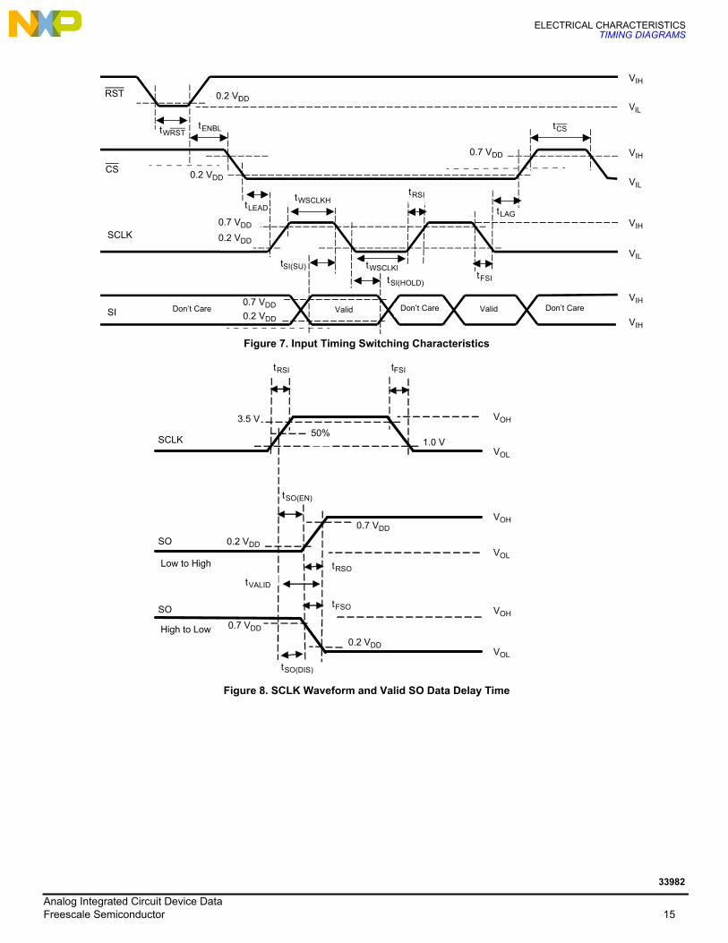
Figure 7. Input Timing Switching Characteristics
Figure 8. SCLK Waveform and Valid SO Data Delay Time
SI
RSTB
CSB
SCLK
Don’t Care Don’t Care Don’t CareValid Valid
VIH
VIL
VIH
VIH
VIH
VIL
VIL
VIL
TwRSTB
TleadTwSCLKh TrSI
Tlag
TSIsu TwSCLKl
TSI(hold)TfSI
0.7 VDD
0.2 VDD
0.7VDD
0.2VDD
0.2VDD
0.7VDD
0.7VDD
TCSB
TENBL
RST
SCLK
SI
CS
0.2 VDD
tWRSTtENBL
0.2 VDD
tLEADtWSCLKH
tRSI
0.7 VDD
0.2 VDD
0.7 VDD
0.2 VDD
tSI(SU) tWSCLKl
tSI(HOLD)tFSI
0.7 VDD
tCS
tLAG
VIH
VIH
VIL
VIL
VIH
VIL
VIH
VIH
SO
SO
SCLK
VOH
VOL
VOH
VOL
VOH
VOL
TfSI
TdlyLH
TdlyHL
TVALID
TrSO
TfSO
3.5V 50%
TrSI
High-to-Low
1.0V
0.7 VDD
0.2VDD
0.2 VDD
0.7 VDD
Low-to-High
tRSI tFSI
0.7 VDD
SCLK
SO
SO
VOH
VOL
VOH
VOL
VOH
VOL
1.0 V
0.2 VDD
0.7 VDD
tRSO
tFSO
0.2 VDD
tSO(EN)
tSO(DIS)
3.5 V
Low to High
High to Low
tVALID
Analog Integrated Circuit Device DataFreescale Semiconductor 15
33982
FUNCTIONAL DESCRIPTIONINTRODUCTION
FUNCTIONAL DESCRIPTION
INTRODUCTION
The 33982 is a self-protected silicon 2.0 m high-side switch used to replace electromechanical relays, fuses, and discrete devices in power management applications. The 33982 is designed for harsh environments, including self-recovery features. The device is suitable for loads with high inrush current, as well as motors and all types of resistive and inductive loads.Programming, control, and diagnostics are implemented via the Serial Peripheral Interface (SPI). A dedicated parallel input is available for alternate and pulse width modulation (PWM) control of the output. SPI programmable fault trip thresholds allow the device to be adjusted for optimal performance in the application. The 33982 is packaged in a power-enhanced 12 mm x 12 mm non-leaded PQFN package with exposed tabs.
FUNCTIONAL PIN DESCRIPTION
OUTPUT CURRENT MONITORING (CSNS)The CSNS pin outputs a current proportional to the high-side output current and used externally to generate a ground-referenced voltage for the microcontroller to monitor output current.
WAKE (WAKE)This pin is used to input a logic [1] signal in order to enable the watchdog timer function. An internal clamp protects this pin from high damaging voltages when the output is current limited with an external resistor. This input has a passive internal pull-down.
RESET (RST) This input pin is used to initialize the device configuration and fault registers, as well as place the device in a low-current sleep mode. The pin also starts the watchdog timer when transitioning from logic LOW to logic HIGH. This pin should not be allowed to be logic High until VDD is in regulation. This pin has a passive internal pull-down.
DIRECT IN (IN)The Input pin is used to directly control the output. This input has an active internal pull-down current source and requires CMOS logic levels. This input may be configured via the SPI.
FAULT STATUS (FS)This is an open drain configured output requiring an external pull-up resistor to VDD for fault reporting. When a device fault condition is detected, this pin is active LOW. Specific device diagnostic faults are reported via the SPI SO pin.
FAIL-SAFE INPUT (FSI)The value of the resistance connected between this pin and ground determines the state of the output after a watchdog timeout occurs. Depending on the resistance value, either the output is OFF or ON. When the FSI pin is connected to GND, the watchdog circuit and Fail-safe operation are disabled. This pin incorporates an active internal pull-up current source.
CHIP SELECT (CS)This input pin is connected to a chip select output of a master microcontroller (MCU). The MCU determines which device is addressed (selected) to receive data by pulling the CS pin of the selected device logic Low, enabling SPI communication with the device. Other unselected devices on the serial link having their CS pins pulled up logic High disregard the SPI communication data sent. This pin incorporates an active internal pull-up current source.
SERIAL CLOCK (SCLK)This input pin is connected to the MCU providing the required bit shift clock for SPI communication. It transitions one time per bit transferred at an operating frequency, fSPI, defined by the communication interface. The 50 percent duty cycle CMOS-level serial clock signal is idle between command transfers. The signal is used to shift data into and out of the device. This input has an active internal pull-down current source.
SERIAL INTERFACE (SI)This is a command data input pin connected to the SPI Serial Data Output of the MCU or to the SO pin of the previous device in a daisy chain of devices. The input requires CMOS logic level signals and incorporates an active internal pull-down current source. Device control is facilitated by the input's receiving the MSB first of a serial 8-bit control command. The MCU ensures data is available upon the falling edge of SCLK. The logic state of SI present upon the rising edge of SCLK loads that bit command into the internal command shift register.
Analog Integrated Circuit Device Data16 Freescale Semiconductor
33982

FUNCTIONAL DESCRIPTIONFUNCTIONAL PIN DESCRIPTION
DIGITAL DRAIN VOLTAGE POWER (VDD)This is an external voltage input pin used to supply power to the SPI circuit. In the event VDD is lost, an internal supply provides power to a portion of the logic, ensuring limited functionality of the device. All device configuration registers are reset.
SERIAL OUTPUT (SO)This output pin is connected to the SPI Serial Data Input pin of the MCU or to the SI pin of the next device in a daisy chain of devices. This output remains tri-stated (high-impedance OFF condition) so long as the CS pin of the device is logic High. SO is only active when the CS pin of the device is asserted logic Low. The generated SO output signals are CMOS logic levels. SO output data is available on the falling edge of SCLK and transitions immediately on the rising edge of SCLK.
POSITIVE POWER SUPPLY (VPWR) This pin connects to the positive power supply and is the source input of operational power for the device. The VPWR pin is a backside surface mount tab of the package.
HIGH-SIDE OUTPUT (HS)This pin protects high-side power output to the load. Output pins must be connected in parallel for operation.
Analog Integrated Circuit Device DataFreescale Semiconductor 17
33982

FUNCTIONAL DESCRIPTIONFUNCTIONAL INTERNAL BLOCK DESCRIPTION
FUNCTIONAL INTERNAL BLOCK DESCRIPTION
Figure 9. Functional Internal Block Diagram
POWER SUPPLYThe 33982 is designed to operate from 4.0 V to 28 V on the VPWR pin. Characteristics are provided from 6.0 V to 20 V for the device. The VPWR pin supplies power to internal regulator, analog, and logic circuit blocks. The VDD supply is used for serial peripheral interface (SPI) communication in order to configure and diagnose the device. This IC architecture provides a low quiescent current sleep mode. Applying VPWR and VDD to the device places the device in the Normal mode. The device transits to Fail-safe mode in case of failures on the SPI (watchdog timeout).
HIGH-SIDE SWITCH: HSThis pin is the high-side output controlling multiple automotive loads with high inrush current, as well as motors and all types of resistive and inductive loads. This N-channel MOSFET with a 2.0 mRDS(on), is self-protected and presents extended diagnostics to detect load disconnections and short-circuit fault conditions. The HS output is actively clamped during a turn-off of inductive loads.
MCU INTERFACE AND OUTPUT CONTROLIn Normal mode, the load is controlled directly from the MCU through the SPI. With a dedicated SPI command, it is possible to independently turn on and off several loads that are PWMed at the same frequency, and duty cycles with only one PWM signal. An analog feedback output provides a current proportional to the load current. The SPI is used to configure and to read the diagnostic status (faults) of high-side output. The reported fault conditions are: open load, short-circuit to ground (OCLO-resistive and OCHI-severe short-circuit), thermal shutdown, and under/overvoltage. In Fail-safe mode, the load is controlled with dedicated parallel input pins. The device is configured in default mode.
MCU Interface and Output Control
MC33982 - Functional Block Diagram
Power Supply
Self-protectedHigh-side Switch
HS
Parallel Control Inputs
Power Supply
MCU Interface and Output Control
SPI Interface
High-side Switch
Analog Integrated Circuit Device Data18 Freescale Semiconductor
33982
FUNCTIONAL DEVICE OPERATIONOPERATIONAL MODES
FUNCTIONAL DEVICE OPERATION
OPERATIONAL MODES
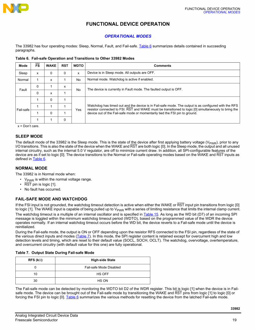
The 33982 has four operating modes: Sleep, Normal, Fault, and Fail-safe. Table 6 summarizes details contained in succeeding paragraphs.
SLEEP MODE The default mode of the 33982 is the Sleep mode. This is the state of the device after first applying battery voltage (VPWR), prior to any I/O transitions. This is also the state of the device when the WAKE and RST are both logic [0]. In the Sleep mode, the output and all unused internal circuitry, such as the internal 5.0 V regulator, are off to minimize current draw. In addition, all SPI-configurable features of the device are as if set to logic [0]. The device transitions to the Normal or Fail-safe operating modes based on the WAKE and RST inputs as defined in Table 6.
NORMAL MODEThe 33982 is in Normal mode when:
• VPWR is within the normal voltage range.• RST pin is logic [1].• No fault has occurred.
FAIL-SAFE MODE AND WATCHDOGIf the FSI input is not grounded, the watchdog timeout detection is active when either the WAKE or RST input pin transitions from logic [0] to logic [1]. The WAKE input is capable of being pulled up to VPWR with a series of limiting resistance that limits the internal clamp current.The watchdog timeout is a multiple of an internal oscillator and is specified in Table 15. As long as the WD bit (D7) of an incoming SPI message is toggled within the minimum watchdog timeout period (WDTO), based on the programmed value of the WDR the device operates normally. If an internal watchdog timeout occurs before the WD bit, the device reverts to a Fail-safe mode until the device is reinitialized. During the Fail-safe mode, the output is ON or OFF depending upon the resistor RFS connected to the FSI pin, regardless of the state of the various direct inputs and modes (Table 7). In this mode, the SPI register content is retained except for overcurrent high and low detection levels and timing, which are reset to their default value (SOCL, SOCH, OCLT). The watchdog, overvoltage, overtemperature, and overcurrent circuitry (with default value for this one) are fully operational.
The Fail-safe mode can be detected by monitoring the WDTO bit D2 of the WDR register. This bit is logic [1] when the device is in Fail-safe mode. The device can be brought out of the Fail-safe mode by transitioning the WAKE and RST pins from logic [1] to logic [0] or forcing the FSI pin to logic [0]. Table 6 summarizes the various methods for resetting the device from the latched Fail-safe mode.
Table 6. Fail-safe Operation and Transitions to Other 33982 Modes
Mode FS WAKE RST WDTO Comments
Sleep x 0 0 x Device is in Sleep mode. All outputs are OFF.
Normal 1 x 1 No Normal mode. Watchdog is active if enabled.
Fault0 1 x
No The device is currently in Fault mode. The faulted output is OFF.0 x 1
Fail-safe
1 0 1
YesWatchdog has timed out and the device is in Fail-safe mode. The output is as configured with the RFS resistor connected to FSI. RST and WAKE must be transitioned to logic [0] simultaneously to bring the device out of the Fail-safe mode or momentarily tied the FSI pin to ground.
1 1 1
1 0 1
1 1 0
x = Don’t care.
Table 7. Output State During Fail-safe Mode
RFS (k) High-side State
0 Fail-safe Mode Disabled
10 HS OFF
30 HS ON
Analog Integrated Circuit Device DataFreescale Semiconductor 19
33982
FUNCTIONAL DEVICE OPERATIONPROTECTION AND DIAGNOSTIC FEATURES
If the FSI pin is tied to GND, the Watchdog Fail-safe operation is disabled.
LOSS OF VDD
If the external 5.0 V supply is not within specification, or even disconnected, all register content is reset. The output can still be driven by the direct input IN. The 33982 uses the battery input to power the output MOSFET related current sense circuitry, and any other internal logic, providing fail-safe device operation with no VDD supplied. In this state, the watchdog, overvoltage, overtemperature, and overcurrent circuitry are fully operational with default values. Current recopy is active with the default current recopy value.
FAULT MODEThe 33982 indicates the following faults as they occur by driving the FS pin to logic [0]: • Overtemperature fault• Overvoltage and undervoltage fault• Open load fault• Overcurrent fault (high and low)
The FS pin automatically returns to logic [1] when the fault condition is removed, except for overcurrent and in some cases undervoltage. Fault information is retained in the fault register and is available (and reset) via the SO pin during the first valid SPI communication (refer to Table 17).
PROTECTION AND DIAGNOSTIC FEATURES
OVERTEMPERATURE FAULT (NON-LATCHING)The 33982 incorporates overtemperature detection and shutdown circuitry in the output structure. Overtemperature detection is enabled when the output is in the ON state. For the output, an overtemperature fault (OTF) condition results in the faulted output turning OFF until the temperature falls below the TSD(HYS). This cycle continues indefinitely until action is taken by the MCU to shut OFF the output, or until the offending load is removed.When experiencing this fault, the OTF fault bit is set in the status register and cleared after either a valid SPI read or a power reset of the device.
OVERVOLTAGE FAULT (NON-LATCHING)The 33982 shuts down the output during an overvoltage fault (OVF) condition on the VPWR pin. The output remains in the OFF state until the overvoltage condition is removed. When experiencing this fault, the OVF fault bit is set in bit OD1 and cleared after either a valid SPI read or a power reset of the device. The overvoltage protection and diagnostic can be disabled through the SPI (bit OV_dis).
UNDERVOLTAGE SHUTDOWN (LATCHING OR NON-LATCHING)The output(s) latches off at some battery voltage below 6.0 V. As long as the VDD level stays within the normal specified range, the internal logic states within the device is sustained.In cases where the battery voltage drops below the undervoltage threshold, (VPWRUV) the output turns off, FS goes to logic [0], and the fault register UVF bit is set to 1.Two cases need to be considered when the battery level recovers:
• If the output(s) command is (are) low, FS goes to logic [1], but the UVF bit remains set to 1 until the next read operation.• If the output command is ON, then FS remains at logic [0]. The output must be turned OFF and ON again to re-enable the state of
output and release FS. The UVF bit remains set to 1 until the next read operation.
The undervoltage protection can be disabled through the SPI (bit UV_dis = 1). In this case, the FS and UVF bits do not report any undervoltage fault condition and the output state is not changed as long as the battery voltage does not drop any lower than 2.5 V.
OPEN LOAD FAULT (NON-LATCHING)The 33982 incorporates open load detection circuitry on the output. Output open load fault (OLF) is detected and reported as a fault condition when the output is disabled (OFF). The open load fault is detected and latched into the status register after the internal gate voltage is pulled low enough to turn OFF the output. The OLF fault bit is set in the status register. If the open load fault is removed, the status register is cleared after reading the register. The open load protection can be disabled through the SPI (bit OL_dis). It is recommended to disable the open load detection circuitry: (OL_dis bit sets to logic [1]) in case of a permanent open load fault condition.
OVERCURRENT FAULT (LATCHING)The 33982 has eight programmable overcurrent low detection levels (IOCL) and two programmable overcurrent high detection levels (IOCH) for maximum device protection. The two selectable, simultaneously active overcurrent detection levels, defined by IOCH and IOCL, are illustrated in Figure 6. The eight different overcurrent low detection levels (IOCL0 : IOCL7) are likewise illustrated in Figure 6.
Analog Integrated Circuit Device Data20 Freescale Semiconductor
33982
FUNCTIONAL DEVICE OPERATIONPROTECTION AND DIAGNOSTIC FEATURES
If the load current level ever reaches the selected overcurrent low detection level and the overcurrent condition exceeds the programmed overcurrent time period (tOCx), the device latches the output OFF.If at any time the current reaches the selected IOCH level, then the device immediately latches the fault and turn OFF the output, regardless of the selected tOCL driver. For both cases, the device output stays off indefinitely until the device is commanded OFF and then ON again.
REVERSE BATTERY The output survives the application of reverse voltage as low as -16 V. Under these conditions, the output’s gate is enhanced to keep the junction temperature less than 150 °C. The ON resistance of the output is fairly similar to that in the Normal mode. No additional passive components are required.
GROUND DISCONNECT PROTECTIONIn the event the 33982 ground is disconnected from load ground, the device protects itself and safely turns OFF the output regardless the state of the output at the time of disconnection. A 10 k resistor needs to be added between the WAKE pin and the rest of the circuitry in order to ensure that the device turns off in case of a ground disconnect and to prevent this pin to exceed its maximum ratings.
Table 8. Device Behavior in Case of Undervoltage
High-side Switch (VPWR
Battery Voltage)
StateUV Enable
IN = 0(Falling VPWR)
UV EnableIN = 0
(Rising VPWR)
UV EnableIN = 1
(Falling VPWR)
UV EnableIN = 1
(Rising VPWR)
UV DisableIN = 0
(Falling or Rising VPWR)
UV DisableIN = 1
(Falling or Rising VPWR)
VPWR > VPWRUV
Output State OFF OFF ON OFF OFF ON
FS State 1 1 1 0 1 1
SPI Fault Register UVF Bit 0 1 until next read 0 1 0 0
VPWRUV > VPWR > UVPOR
Output State OFF OFF OFF OFF OFF ON
FS State 0 0 0 0 1 1
SPI Fault Register UVF Bit 1 1 1 1 0 0
UVPOR > VPWR > 2.5 V
Output State OFF OFF OFF OFF OFF ON
FS State 1 1 1 1 1 1
SPI Fault Register UVF Bit 1 until next read 1 1 until next read 1 until next read 0 0
2.5 V > VPWR > 0 V
Output State OFF OFF OFF OFF OFF OFF
FS State 1 1 1 1 1 1
SPI Fault Register UVF Bit 1 until next read 1 until next read 1 until next read 1 until next read 0 0
Comments UV fault is not latched
UV fault is not latched
UV fault is latched
Typical value; not guaranteed While VDD remains within specified range.= IN is equivalent to IN direct input or IN_spi SPI input.
Analog Integrated Circuit Device DataFreescale Semiconductor 21
33982

FUNCTIONAL DEVICE OPERATIONLOGIC COMMANDS AND REGISTERS
FUNCTIONAL DEVICE OPERATION
LOGIC COMMANDS AND REGISTERS
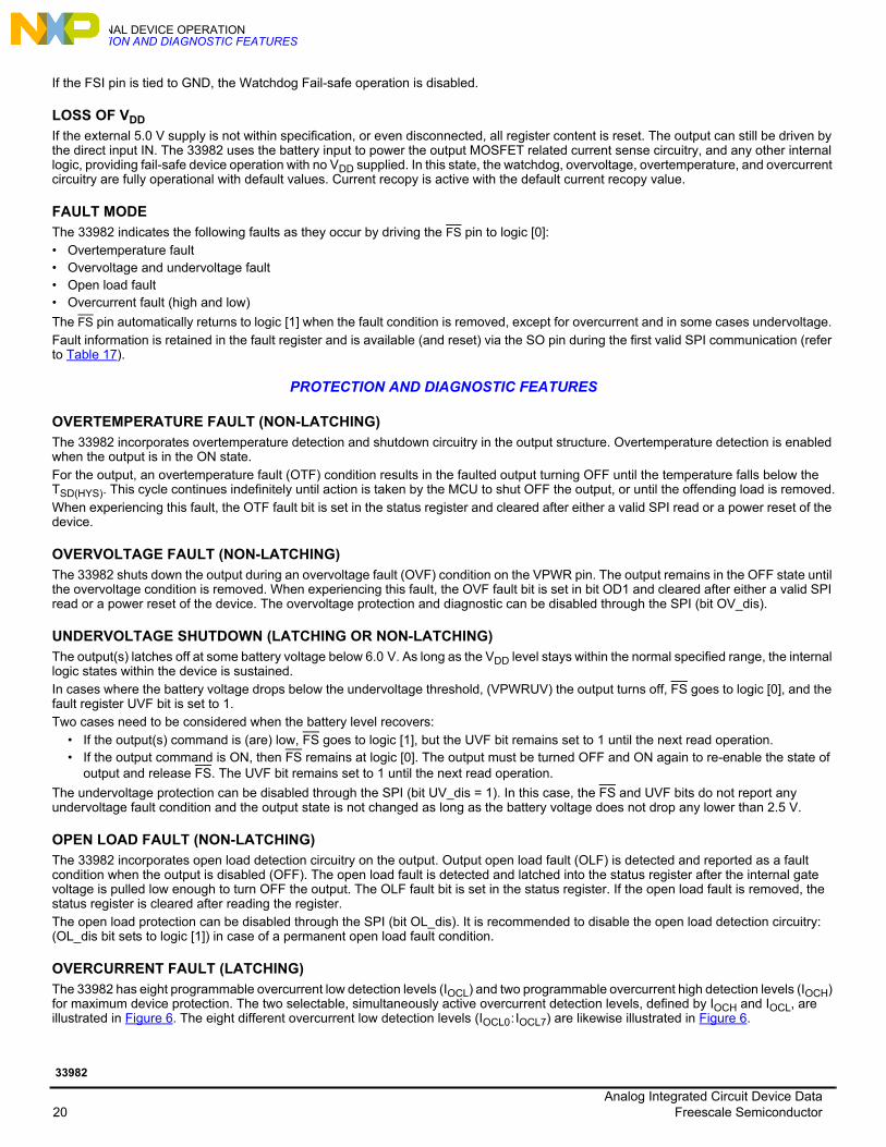
SPI PROTOCOL DESCRIPTION The SPI interface has a full duplex, three-wire synchronous data transfer with four I /O lines associated with it: Serial Clock (SCLK), Serial Input (SI), Serial Output (SO), and Chip Select (CS). The SI / SO pins of the 33982 follow a first-in first-out (D7 / D0) protocol with both input and output words transferring the most significant bit (MSB) first. All inputs are compatible with 5.0 V CMOS logic levels. The SPI lines perform the following functions:
SERIAL CLOCK (SCLK)The SCLK pin clocks the internal shift registers of the 33982 device. The serial input pin (SI) accepts data into the input shift register on the falling edge of the SCLK signal while the serial output pin (SO) shifts data information out of the SO line driver on the rising edge of the SCLK signal. It is important that the SCLK pin be in a logic LOW state whenever CS makes any transition. For this reason, it is recommended that the SCLK pin be in a logic [0] state whenever the device is not accessed (CS logic [1] state). SCLK has an active internal pull-down, IDWN. When CS is logic [1], signals at the SCLK and SI pins are ignored and SO is tri-stated (high-impedance). (See Figure 10 and Figure 11.)
SERIAL INTERFACE (SI)This is a serial interface (SI) command data input pin. SI instruction is read on the falling edge of SCLK. An 8-bit stream of serial data is required on the SI pin, starting with D7 to D0. The internal registers of the 33982 are configured and controlled using a 4-bit addressing scheme, as shown in Table 9. Register addressing and configuration are described in Table 10. The SI input has an active internal pull-down, IDWN.
SERIAL OUTPUT (SO)The SO pin is a tri-stateable output from the shift register. The SO pin remains in a high-impedance state until the CS pin is put into a logic [0] state. The SO data is capable of reporting the status of the output, the device configuration, and the state of the key inputs. The SO pin changes states on the rising edge of SCLK and reads out on the falling edge of SCLK. Fault and input status descriptions are provided in Table 16.
CHIP SELECT (CS)The CS pin enables communication with the master microcontroller (MCU). When this pin is in a logic [0] state, the device is capable of transferring information to and receiving information from the MCU. The 33982 latches in data from the input shift registers to the addressed registers on the rising edge of CS. The device transfers status information from the power output to the shift register on the falling edge of CS. The SO output driver is enabled when CS is logic [0]. CS should transition from a logic [1] to a logic [0] state only when SCLK is a logic [0]. CS has an active internal pull-up, IUP.
Figure 10. Single 8-Bit Word SPI Communication
CSB
SI
SCLK
D7 D1D2D3D4D5D6 D0
OD7 OD6 OD1OD2OD3OD4OD5
NOTES:
OD0SO
1. RSTB is in a logic 1 state during the above operation.2. D0, D1, D2, ..., and D7 relate to the most recent ordered entry of data into the SPSS3. OD0, OD1, OD2, ..., and OD7 relate to the first 8 bits of ordered fault and status data out
of the device.
CS
SO
RST1. RST is a logic [1] state during the above operation.2. D7:D0 relate to the most recent ordered entry of data into the device.3. OD7:OD0 relate to the first 8 bits of ordered fault and status data out of the device.
Notes
Analog Integrated Circuit Device Data22 Freescale Semiconductor
33982
FUNCTIONAL DEVICE OPERATIONLOGIC COMMANDS AND REGISTERS
Figure 11. Multiple 8-Bit Word SPI Communication
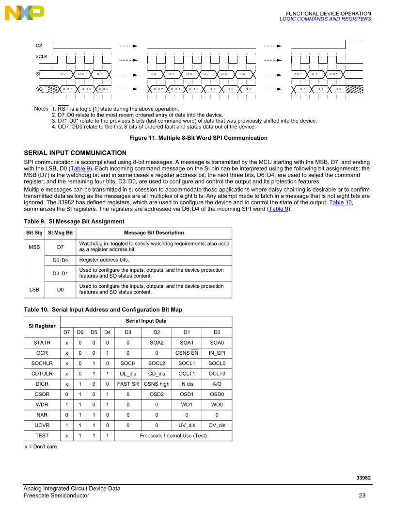
SERIAL INPUT COMMUNICATIONSPI communication is accomplished using 8-bit messages. A message is transmitted by the MCU starting with the MSB, D7, and ending with the LSB, D0 (Table 9). Each incoming command message on the SI pin can be interpreted using the following bit assignments: the MSB (D7) is the watchdog bit and in some cases a register address bit; the next three bits, D6 : D4, are used to select the command register; and the remaining four bits, D3 : D0, are used to configure and control the output and its protection features. Multiple messages can be transmitted in succession to accommodate those applications where daisy chaining is desirable or to confirm transmitted data as long as the messages are all multiples of eight bits. Any attempt made to latch in a message that is not eight bits are ignored. The 33982 has defined registers, which are used to configure the device and to control the state of the output. Table 10, summarizes the SI registers. The registers are addressed via D6 : D4 of the incoming SPI word (Table 9).
Table 9. SI Message Bit Assignment
Bit Sig SI Msg Bit Message Bit Description
MSB D7Watchdog in: toggled to satisfy watchdog requirements; also used as a register address bit.
D6 : D4 Register address bits.
D3 : D1Used to configure the inputs, outputs, and the device protection features and SO status content.
LSB D0Used to configure the inputs, outputs, and the device protection features and SO status content.
Table 10. Serial Input Address and Configuration Bit Map
SI RegisterSerial Input Data
D7 D6 D5 D4 D3 D2 D1 D0
STATR x 0 0 0 0 SOA2 SOA1 SOA0
OCR x 0 0 1 0 0 CSNS EN IN_SPI
SOCHLR x 0 1 0 SOCH SOCL2 SOCL1 SOCL0
CDTOLR x 0 1 1 OL_dis CD_dis OCLT1 OCLT0
DICR x 1 0 0 FAST SR CSNS high IN dis A/O
OSDR 0 1 0 1 0 OSD2 OSD1 OSD0
WDR 1 1 0 1 0 0 WD1 WD0
NAR 0 1 1 0 0 0 0 0
UOVR 1 1 1 0 0 0 UV_dis OV_dis
TEST x 1 1 1 Freescale Internal Use (Test)
x = Don’t care.
C S B
S I
S C L K
D 7 D 1 *D 2 *D 5 *D 6 *D 7 *D 0D 1D 6 D 5 D 2 D 0 *
O D 5O D 6O D 7 D 6D 7O D 0O D 1O D 2 D 1D 2D 5
F I G U R E 4 b . M U L T I P L E 8 b i t W O R D S P I C O M M U N I C A T I O N
N O T E S :
D 0S O
1 . R S T B i s i n a l o g i c 1 s t a t e d u r i n g t h e a b o v e o p e r a t i o n .2 . D 0 , D 1 , D 2 , . . . , a n d D 7 r e l a t e t o t h e m o s t r e c e n t o r d e r e d e n t r y o f d a t a i n t o t h e S P S S3 . O D 0 , O D 1 , O D 2 , . . . , a n d O D 7 r e l a t e t o t h e f i r s t 8 b i t s o f o r d e r e d f a u l t a n d s t a t u s d a t a o u t o f t h e d e v i c e .4 . O D 0 , O D 1 , O D 2 , . . . , a n d O D 7 r e p r e s e n t t h e f i r s t 8 b i t s o f o r d e r e d f a u l t a n d s t a t u s d a t a o u t o f t h e S P S S
CS
SCLK
SI
SO
R S T1. RST is a logic [1] state during the above operation.2. D7:D0 relate to the most recent ordered entry of data into the device.
4. OD7:OD0 relate to the first 8 bits of ordered fault and status data out of the device.
Notes
3. D7*:D0* relate to the previous 8 bits (last command word) of data that was previously shifted into the device.
Analog Integrated Circuit Device DataFreescale Semiconductor 23
33982

FUNCTIONAL DEVICE OPERATIONLOGIC COMMANDS AND REGISTERS
DEVICE REGISTER ADDRESSINGThe following section describes the possible register addresses and their impact on device operation.
Address x000 — Status Register (STATR)
The STATR register is used to read the device status and the various configuration register contents without disrupting the device operation or the register contents. The register bits D2, D1, and D0 determine the content of the first eight bits of SO data. In addition to the device status, this feature provides the ability to read the content of the OCR, SOCHLR, CDTOLR, DICR, OSDR, WDR, NAR, and UOVR registers. (Refer to the section entitled Serial Output Communication (Device Status Return Data) beginning on page 26.)
Address x001 — Output Control Register (OCR)
The OCR register allows the MCU to control the output through the SPI. Incoming message bit D0 (IN_SPI) reflects the desired states of the high-side output: a logic [1] enables the output switch and a logic [0] turns it OFF. A logic [1] on message bit D1 enables the Current Sense (CSNS) pin. Bits D2 and D3 must be logic [0]. Bit D7 is used to feed the watchdog if enabled.
Address x010 — Select Overcurrent High and Low Register (SOCHLR)
The SOCHLR register allows the MCU to configure the output overcurrent low and high detection levels, respectively. In addition to protecting the device, this slow blow fuse emulation feature can be used to optimize the load requirements to match system characteristics. Bits D2 : D0 are used to set the overcurrent low detection level to one of eight possible levels as defined in Table 11. Bit D3 is used to set the overcurrent high detection level to one of two levels as defined in Table 12.
Address x011 — Current Detection Time and Open Load Register (CDTOLR)
The CDTOLR register is used by the MCU to determine the amount of time the device allows an overcurrent low condition before output latches OFF occurs. Bits D1 and D0 allow the MCU to select one of four fault blanking times defined in Table 13. Note that these timeouts apply only to the overcurrent low detection levels. If the selected overcurrent high level is reached, the device latchs off within 20 s.
A logic [1] on bit D2 disables the overcurrent low (CD_dis) detection timeout feature. A logic [1] on bit D3 disables the open load (OL) detection feature.
Table 11. Overcurrent Low Detection Levels
SOCL2 (D2) SOCL1 (D1) SOCL0 (D0) Overcurrent Low Detection (Amperes)
0 0 0 50
0 0 1 45
0 1 0 40
0 1 1 35
1 0 0 30
1 0 1 25
1 1 0 20
1 1 1 15
Table 12. Overcurrent High Detection Levels
SOCH (D3) Overcurrent High Detection (Amperes)
0 150
1 100
Table 13. Overcurrent Low Detection Blanking Time
OCLT [1:0] Timing
00 155 ms
01 10 ms
10 1.2 ms
11 150 s
Analog Integrated Circuit Device Data24 Freescale Semiconductor
33982

FUNCTIONAL DEVICE OPERATIONLOGIC COMMANDS AND REGISTERS
Address x100 — Direct Input Control Register (DICR)
The DICR register is used by the MCU to enable, disable, or configure the direct IN pin control of the output. A logic [0] on bit D1 enables the output for direct control by the IN pin. A logic [1] on bit D1 disables the output from direct control. While addressing this register, if the input was enabled for direct control, a logic [1] for the D0 bit results in a Boolean AND of the IN pin with its corresponding D0 message bit when addressing the OCR register. Similarly, a logic [0] on the D0 pin results in a Boolean OR of the IN pin with the corresponding message bits when addressing the OCR register. The DICR register is useful if there is a need to independently turn on and off several loads that are PWMed at the same frequency and duty cycle with only one PWM signal. This type of operation can be accomplished by connecting the pertinent direct IN pins of several devices to a PWM output port from the MCU, and configuring each of the outputs to be controlled via their respective direct IN pin. The DICR is then used to Boolean AND the direct IN(s) of each of the outputs with the dedicated SPI bit that also controls the output. Each configured SPI bit can now be used to enable and disable the common PWM signal from controlling its assigned output.A logic [1] on bit D2 is used to select the high ratio (CSR1, 1/40000) on the CSNS pin. The default value [0] is used to select the low ratio (CSR0, 1/5400). A logic [1] on bit D3 is used to select the high-speed slew rate. The default value [0] corresponds to the low-speed slew rate.
Address 0101 — Output Switching Delay Register (OSDR)
The OSDR register is used to configure the device with a programmable time delay that is active during Output On transitions that are initiated via the SPI (not via direct input). Whenever the input is commanded to transition from logic [0] to logic [1], the output are held OFF for the time delay configured in the OSDR register. The programming of the contents of this register has no effect on device Fail-safe mode operation. The default value of the OSDR register is 000, equating to no delay, since the switching delay time is 0 ms. This feature allows the user a way to minimize inrush currents, or surges, thereby allowing loads to be synchronously switched ON with a single command. Table 14 shows the eight selectable output switching delay times, which range from 0 ms to 525 ms.
Address 1101 — Watchdog Register (WDR)
The WDR register is used by the MCU to configure the watchdog timeout. Watchdog timeout is configured using bits D1 and D0 (Table 15). When bits D1 and D0 are programmed for the desired watchdog timeout period, the WD bit (D7) should be toggled as well to ensure that the new timeout period is programmed at the beginning of a new count sequence.
Address 0110 — No Action Register (NAR)
The NAR register can be used to no-operation fill SPI data packets in a daisy chain SPI configuration. This allows devices to not be affected by commands being clocked over a daisy-chained SPI configuration, and by toggling the WD bit (D7) the watchdog circuitry continues to be reset while no programming or data readback functions are being requested from the device.
Table 14. Switching Delay
OSD[2:0] (D2 : D0) Turn ON Delay (ms)
000 0
001 75
010 150
011 225
100 300
101 375
110 450
111 525
Table 15. Watchdog Timeout
WD [1:0] (D1: D0) Timing (ms)
00 620
01 310
10 2500
11 1250
Analog Integrated Circuit Device DataFreescale Semiconductor 25
33982
FUNCTIONAL DEVICE OPERATIONLOGIC COMMANDS AND REGISTERS
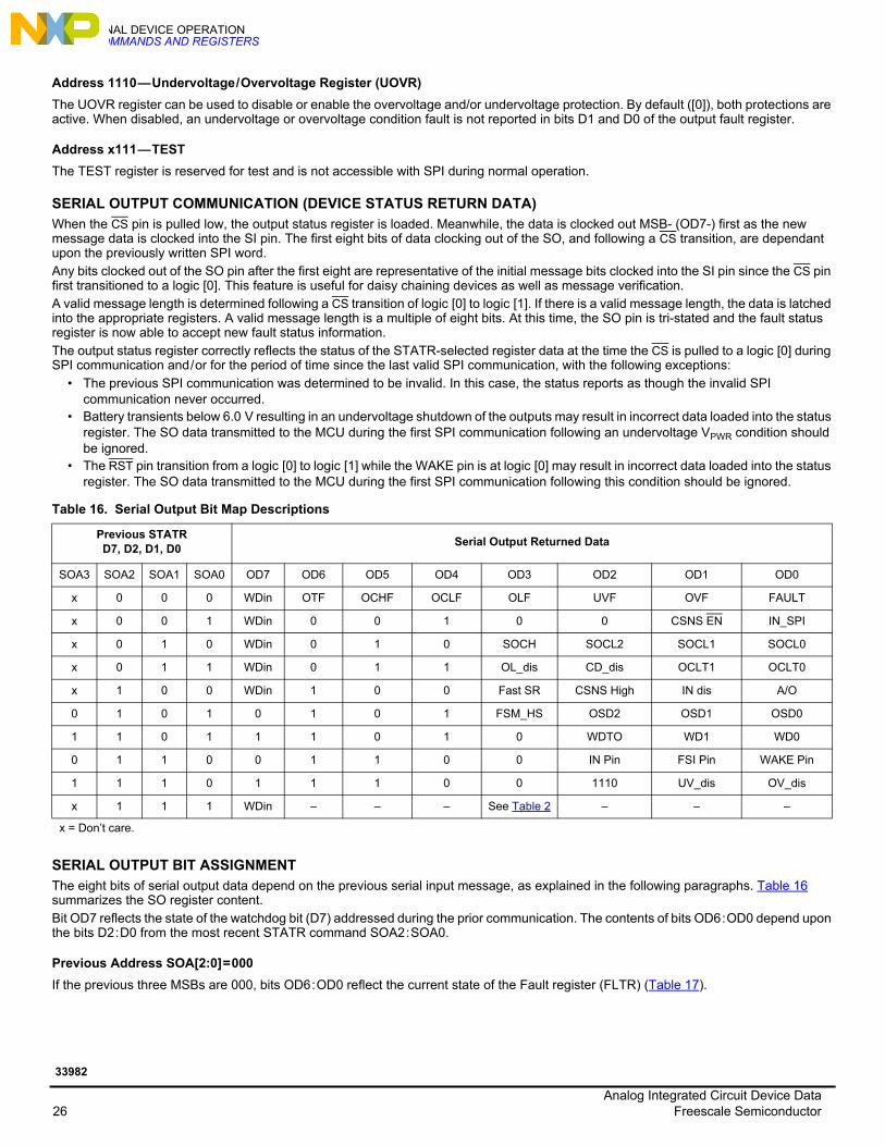
Address 1110 — Undervoltage / Overvoltage Register (UOVR)
The UOVR register can be used to disable or enable the overvoltage and/or undervoltage protection. By default ([0]), both protections are active. When disabled, an undervoltage or overvoltage condition fault is not reported in bits D1 and D0 of the output fault register.
Address x111 — TEST
The TEST register is reserved for test and is not accessible with SPI during normal operation.
SERIAL OUTPUT COMMUNICATION (DEVICE STATUS RETURN DATA)When the CS pin is pulled low, the output status register is loaded. Meanwhile, the data is clocked out MSB- (OD7-) first as the new message data is clocked into the SI pin. The first eight bits of data clocking out of the SO, and following a CS transition, are dependant upon the previously written SPI word.Any bits clocked out of the SO pin after the first eight are representative of the initial message bits clocked into the SI pin since the CS pin first transitioned to a logic [0]. This feature is useful for daisy chaining devices as well as message verification.A valid message length is determined following a CS transition of logic [0] to logic [1]. If there is a valid message length, the data is latched into the appropriate registers. A valid message length is a multiple of eight bits. At this time, the SO pin is tri-stated and the fault status register is now able to accept new fault status information.The output status register correctly reflects the status of the STATR-selected register data at the time the CS is pulled to a logic [0] during SPI communication and / or for the period of time since the last valid SPI communication, with the following exceptions:
• The previous SPI communication was determined to be invalid. In this case, the status reports as though the invalid SPI communication never occurred.
• Battery transients below 6.0 V resulting in an undervoltage shutdown of the outputs may result in incorrect data loaded into the status register. The SO data transmitted to the MCU during the first SPI communication following an undervoltage VPWR condition should be ignored.
• The RST pin transition from a logic [0] to logic [1] while the WAKE pin is at logic [0] may result in incorrect data loaded into the status register. The SO data transmitted to the MCU during the first SPI communication following this condition should be ignored.
SERIAL OUTPUT BIT ASSIGNMENTThe eight bits of serial output data depend on the previous serial input message, as explained in the following paragraphs. Table 16 summarizes the SO register content.Bit OD7 reflects the state of the watchdog bit (D7) addressed during the prior communication. The contents of bits OD6 : OD0 depend upon the bits D2 : D0 from the most recent STATR command SOA2 : SOA0.
Previous Address SOA[2:0] = 000
If the previous three MSBs are 000, bits OD6 : OD0 reflect the current state of the Fault register (FLTR) (Table 17).
Table 16. Serial Output Bit Map Descriptions
Previous STATR D7, D2, D1, D0
Serial Output Returned Data
SOA3 SOA2 SOA1 SOA0 OD7 OD6 OD5 OD4 OD3 OD2 OD1 OD0
x 0 0 0 WDin OTF OCHF OCLF OLF UVF OVF FAULT
x 0 0 1 WDin 0 0 1 0 0 CSNS EN IN_SPI
x 0 1 0 WDin 0 1 0 SOCH SOCL2 SOCL1 SOCL0
x 0 1 1 WDin 0 1 1 OL_dis CD_dis OCLT1 OCLT0
x 1 0 0 WDin 1 0 0 Fast SR CSNS High IN dis A/O
0 1 0 1 0 1 0 1 FSM_HS OSD2 OSD1 OSD0
1 1 0 1 1 1 0 1 0 WDTO WD1 WD0
0 1 1 0 0 1 1 0 0 IN Pin FSI Pin WAKE Pin
1 1 1 0 1 1 1 0 0 1110 UV_dis OV_dis
x 1 1 1 WDin – – – See Table 2 – – –
x = Don’t care.
Analog Integrated Circuit Device Data26 Freescale Semiconductor
33982

FUNCTIONAL DEVICE OPERATIONLOGIC COMMANDS AND REGISTERS
Previous Address SOA[2:0] = 001
The data in bits OD1 and OD0 contain CSNS EN and IN_SPI programmed bits, respectively.
Previous Address SOA[2:0] = 010
The data in bit OD3 contain the programmed overcurrent high detection level (refer to Table 12), and the data in bits OD2, OD1, and OD0 contain the programmed overcurrent low detection levels (refer to Table 11).
Previous Address SOA[2:0] = 011
The data returned in bits OD1 and OD0 are current values for the overcurrent fault blanking time, illustrated in Table 13. Bit OD2 reports when the overcurrent detection timeout feature is active. OD3 reports whether the open load circuitry is active.
Previous Address SOA[2:0] =100
The returned data contain the programmed values in the DICR.
Previous Address SOA[2:0] =101
• SOA3 = 0. The returned data contain the programmed values in the OSDR. Bit OD3 (FSM_HS) reflects the state of the output in the Fail-safe mode after a watchdog timeout occurs.
• SOA3 = 1. The returned data contain the programmed values in the WDR. Bit OD2 (WDTO) reflects the status of the watchdog circuitry. If WDTO bit is logic [1], the watchdog has timed out and the device is in Fail-safe mode. If WDTO is logic [0], the device is in Normal mode (assuming device is powered and not in the Sleep mode), with the watchdog either enabled or disabled.
Previous Address SOA[2:0] =110
• SOA3 = 0. OD2, OD1, and OD0 return the state of the IN, FSI, and WAKE pins, respectively (Table 18).
• SOA3 = 1. The returned data contains the programmed values in the UOVR register. Bit OD1 reflects the state of the undervoltage protection, while bit OD0 reflects the state of the overvoltage protection (refer to Table 16).
Previous Address SOA[2:0] = 111
Null Data. No previous register Read Back command received, so bits OD2, OD1, and OD0 are null, or 000.
Table 17. Fault Register
OD7 OD6 OD5 OD4 OD3 OD2 OD1 OD0
x OTF OCHF OCLF OLF UVF OVF FAULT
OD7 (x) = Don’t care.
OD6 (OTF) = Overtemperature Flag.
OD5 (OCHF) = Overcurrent High Flag. (This fault is latched.)
OD4 (OCLF) = Overcurrent Low Flag. (This fault is latched.)
OD3 (OLF) = Open Load Flag.
OD2 (UVF) = Undervoltage Flag. (This fault is latched or not latched.)
OD1 (OVF) = Overvoltage Flag.
OD0 (FAULT) = This flag reports a fault and is reset by a read operation.
Note The FS pin reports a fault and is reset by a new Switch-ON command (via SPI or direct input IN).
Table 18. Pin Register
OD2 OD1 OD0
IN Pin FSI Pin WAKE Pin
Analog Integrated Circuit Device DataFreescale Semiconductor 27
33982
TYPICAL APPLICATIONSLOGIC COMMANDS AND REGISTERS
TYPICAL APPLICATIONS
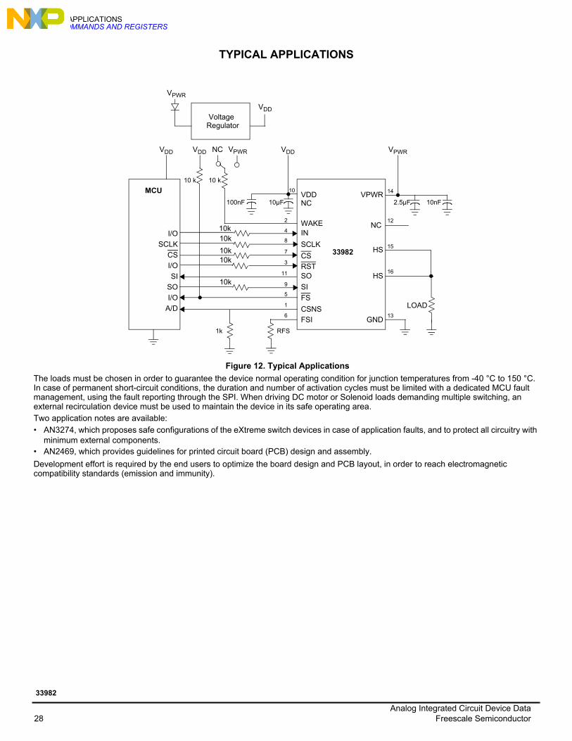
Figure 12. Typical Applications
The loads must be chosen in order to guarantee the device normal operating condition for junction temperatures from -40 °C to 150 °C. In case of permanent short-circuit conditions, the duration and number of activation cycles must be limited with a dedicated MCU fault management, using the fault reporting through the SPI. When driving DC motor or Solenoid loads demanding multiple switching, an external recirculation device must be used to maintain the device in its safe operating area. Two application notes are available: • AN3274, which proposes safe configurations of the eXtreme switch devices in case of application faults, and to protect all circuitry with
minimum external components.• AN2469, which provides guidelines for printed circuit board (PCB) design and assembly.
Development effort is required by the end users to optimize the board design and PCB layout, in order to reach electromagnetic compatibility standards (emission and immunity).
A/D
MCU
I/O
I/O
SI
SO
SCLK
I/O
CS
SO
SI
FS
VDD
FSI
CSNS
RST
CS
IN
SCLK
NC
WAKE
NC VPWR
33982
100nF 10µF
VDD VDD
GND
HS
HS
VPWR
VPWR
2.5µF 10nF
LOAD
RFS1k
10 k 10 k
VDD
10
3
7
8
4
2
9
5
13
1
16
6
15
14
11
VoltageRegulator
VDD
VPWR
NC12
10k
10k10k
10k10k
Analog Integrated Circuit Device Data28 Freescale Semiconductor
33982

PACKAGINGSOLDERING INFORMATION
PACKAGING
SOLDERING INFORMATION
SOLDERING INFORMATIONThe 33982 is packaged in a surface mount power package (PQFN), intended to be soldered directly on the printed circuit board. The AN2467 provides guidelines for Printed Circuit Board design and assembly.
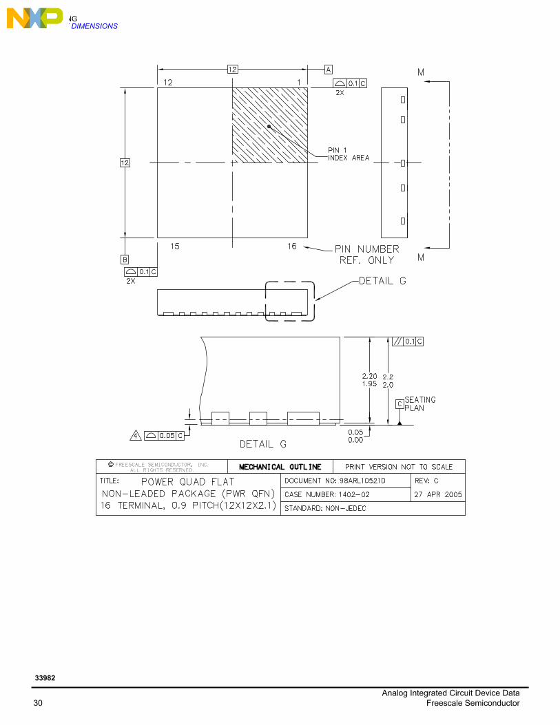
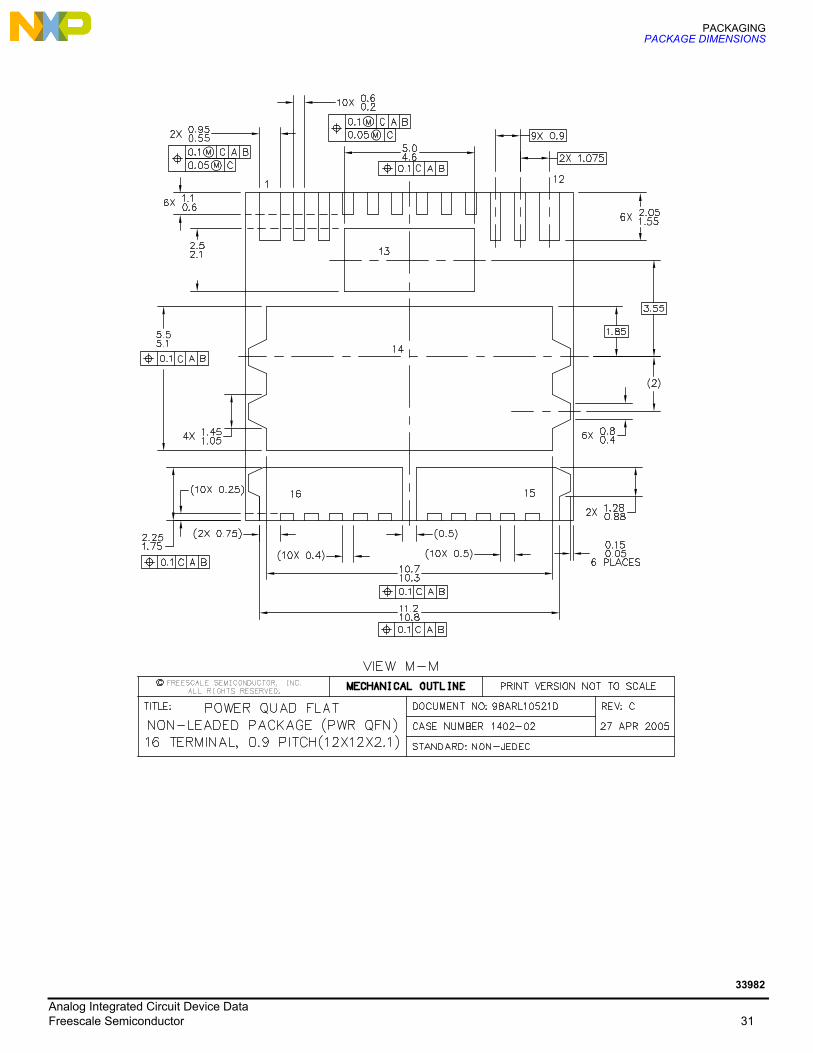
PACKAGE DIMENSIONS
For the most current revision of the package, visit www.freescale.com and perform a keyword search on 98ARL10596D. Dimensions shown are provided for reference ONLY.
Analog Integrated Circuit Device DataFreescale Semiconductor 29
33982
PACKAGINGPACKAGE DIMENSIONS
Analog Integrated Circuit Device Data30 Freescale Semiconductor
33982
PACKAGINGPACKAGE DIMENSIONS
Analog Integrated Circuit Device DataFreescale Semiconductor 31
33982

ADDITIONAL DOCUMENTATIONTHERMAL ADDENDUM (REV 4.0)
ADDITIONAL DOCUMENTATION
THERMAL ADDENDUM (REV 4.0)
Introduction
This thermal addendum is provided as a supplement to the 33982 technical datasheet. The addendum provides thermal performance information that may be critical in the design and development of system applications. All electrical, application, and packaging information is provided in the datasheet.
Packaging and Thermal Considerations
This package is a dual die package. There are two heat sources in the package independently heating with P1 and P2. This results in two junction temperatures, TJ1 and TJ2, and a thermal resistance matrix with RJAmn.For m, n = 1, RJA11 is the thermal resistance from Junction 1 to the reference temperature while only heat source 1 is heating with P1. For m = 1, n = 2, RJA12 is the thermal resistance from Junction 1 to the reference temperature while heat source 2 is heating with P2. This applies to RJ21 and RJ22, respectively.
The stated values are solely for a thermal performance comparison of one package to another in a standardized environment. This methodology is not meant to and does not predict the performance of a package in an application-specific environment. Stated values were obtained by measurement and simulation according to the standards listed below.
Standards
High-side Switch
33982
98ARL10521D16-PIN PQFN
12 mm x 12 mm
Note For package dimensions, refer to 98ARL10521D.
TJ1TJ2
=RJA11RJA21
RJA12RJA22
.P1P2
Table 19. Thermal Performance Comparison
ThermalResistance
1 = Power Chip, 2 = Logic Chip [C/W]
m = 1,n = 1
m = 1, n = 2m = 2, n = 1
m = 2,n = 2
RJAmn (1), (2) 20 16 39
RJBmn (2), (3) 6 2.0 26
RJAmn (1), (4) 53 40 73
RJCmn (5) <0.5 0.0 1.0
Notes:1. Per JEDEC JESD51-2 at natural convection, still air condition.2. 2s2p thermal test board per JEDEC JESD51-7and
JESD51-5.3. Per JEDEC JESD51-8, with the board temperature on the center trace near the
power outputs.4. Single layer thermal test board per JEDEC JESD51-3 and JESD51-5.5. Thermal resistance between the die junction and the exposed pad, “infinite” heat
sink attached to exposed pad.
Analog Integrated Circuit Device Data32 Freescale Semiconductor
33982

ADDITIONAL DOCUMENTATIONTHERMAL ADDENDUM (REV 4.0)
Figure 13. Surface Mount for Power PQFNwith Exposed Pads
Figure 14. Thermal Test Board
Note: Recommended via diameter is 0.5 mm. PTH (plated through hole) via must be plugged / filled with epoxy or solder mask in order to minimize void formation and to avoid any solder wicking into the via.
1.0
1.00.2
0.2
* All measurementsare in millimeters
HS HS1615
VPWR14
GND13
CS
NSINFS
FS
I
CS
SC
LK
RS
T
WA
KESI
VD
D
SO
NC
111 10 9 8 7 6 5 4 3 212
16-Pin PQFN0.90 mm Pitch
12.0 mm x 12.0 mm Body
33982 Pin Connections
Transparent Top View
A
A
Analog Integrated Circuit Device DataFreescale Semiconductor 33
33982
ADDITIONAL DOCUMENTATIONTHERMAL ADDENDUM (REV 4.0)
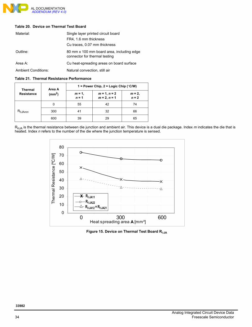
RJAis the thermal resistance between die junction and ambient air. This device is a dual die package. Index m indicates the die that is heated. Index n refers to the number of the die where the junction temperature is sensed.
Figure 15. Device on Thermal Test Board RJA
Table 20. Device on Thermal Test Board
Material: Single layer printed circuit board
FR4, 1.6 mm thickness
Cu traces, 0.07 mm thickness
Outline: 80 mm x 100 mm board area, including edge connector for thermal testing
Area A: Cu heat-spreading areas on board surface
Ambient Conditions: Natural convection, still air
Table 21. Thermal Resistance Performance
Thermal Resistance
Area A
(mm2)
1 = Power Chip, 2 = Logic Chip (C/W)
m = 1,n = 1
m = 1, n = 2m = 2, n = 1
m = 2,n = 2
RJAmn
0 55 42 74
300 41 32 66
600 39 29 65
0
10
20
30
40
50
60
70
80
Heat spreading area A [mm²]
Th
erm
al R
esi
sta
nce
[ºC
/W]
0 300 600
RJA11
RJA22RJA12 = RJA21
x
Analog Integrated Circuit Device Data34 Freescale Semiconductor
33982

ADDITIONAL DOCUMENTATIONTHERMAL ADDENDUM (REV 4.0)
Figure 16. Transient Thermal Resistance RJA (1.0 W Step Response)Device on Thermal Test Board Area A = 600(mm2)
0.1
1
10
100
1.00E-03 1.00E-02 1.00E-01 1.00E+00 1.00E+01 1.00E+02 1.00E+03 1.00E+04Time(s)
The
rmal
Res
ista
nce
(°C
W)
RJA11
RJA22RJA12 = RJA21
x
Analog Integrated Circuit Device DataFreescale Semiconductor 35
33982
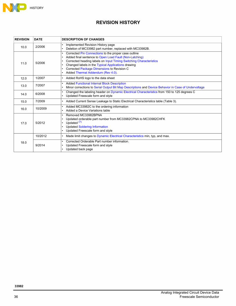
REVISION HISTORY
REVISION HISTORY
REVISION DATE DESCRIPTION OF CHANGES
10.0 2/2006• Implemented Revision History page• Deletion of MC33982 part number, replaced with MC33982B.
11.0 5/2006
• Corrected Pin Connections to the proper case outline• Added final sentence to Open Load Fault (Non-Latching)• Corrected heading labels on Input Timing Switching Characteristics• Changed labels in the Typical Applications drawing• Corrected Package Dimensions to Revision C• Added Thermal Addendum (Rev 4.0).
12.0 1/2007 • Added RoHS logo to the data sheet
13.0 7/2007• Added Functional Internal Block Description• Minor corrections to Serial Output Bit Map Descriptions and Device Behavior in Case of Undervoltage
14.0 6/2008• Changed the labeling header on Dynamic Electrical Characteristics from 150 to 125 degrees C• Updated Freescale form and style
15.0 7/2009 • Added Current Sense Leakage to Static Electrical Characteristics table (Table 3).
16.0 10/2009• Added MC33982C to the ordering information• Added a Device Variations table
17.0 5/2012
• Removed MC33982BPNA• Updated orderable part number from MC33982CPNA to MC33982CHFK• Updated (7)
• Updated Soldering Information• Updated Freescale form and style
18.0
10/2012 • Made limit changes to Dynamic Electrical Characteristics min, typ, and max.
9/2014• Corrected Orderable Part number information.• Updated Freescale form and style• Updated back page
Analog Integrated Circuit Device Data36 Freescale Semiconductor
33982
Document Number: MC33982Rev. 18.0
9/2014
Information in this document is provided solely to enable system and software implementers to use Freescale products.
There are no express or implied copyright licenses granted hereunder to design or fabricate any integrated circuits based
on the information in this document.
Freescale reserves the right to make changes without further notice to any products herein. Freescale makes no
warranty, representation, or guarantee regarding the suitability of its products for any particular purpose, nor does
Freescale assume any liability arising out of the application or use of any product or circuit, and specifically disclaims any
and all liability, including without limitation consequential or incidental damages. “Typical” parameters that may be
provided in Freescale data sheets and/or specifications can and do vary in different applications, and actual performance
may vary over time. All operating parameters, including “typicals,” must be validated for each customer application by
customer’s technical experts. Freescale does not convey any license under its patent rights nor the rights of others.
Freescale sells products pursuant to standard terms and conditions of sale, which can be found at the following address:
freescale.com/SalesTermsandConditions.
Freescale and the Freescale logo are trademarks of Freescale Semiconductor, Inc., Reg. U.S. Pat. & Tm. Off.
SMARTMOS is a trademark of Freescale Semiconductor, Inc. All other product or service names are the property of their
respective owners.
© 2014 Freescale Semiconductor, Inc.
How to Reach Us:
Home Page: freescale.com
Web Support: freescale.com/support