Franz Kreupl - TUM
51
Department of Hybrid Electronic Systems Technische Universität München Carbon Memory Assessment A white paper for the ITRS ERD meeting on August 25-26, 2014, Albuquerque, NM can be downloaded here: http://arxiv.org/abs/1408.4600 Franz Kreupl Technische Universität München (TUM) Department of Hybrid Electronic Systems (HES) [email protected]
Transcript of Franz Kreupl - TUM

Department of Hybrid Electronic Systems Technische Universität München
Carbon Memory Assessment
A white paper for the ITRS ERD meeting on August 25-26, 2014, Albuquerque, NM
can be downloaded here: http://arxiv.org/abs/1408.4600
Franz Kreupl
Technische Universität München (TUM) Department of Hybrid Electronic Systems (HES)

Technische Universität München Department of Hybrid Electronic Systems
Outline: Carbon Memory Assessment Basic Facts about Carbon
Carbon Allotropes Manipulating the Bond Structure of Carbon Sustainable Current Density in Carbon Structures Break-junctions and Plumbing in Carbon Structures
What Is Not Considered as Carbon-based Memory Carbon-based Resistive Memory Phase Diagram First Current Pulse Challenge with Conductive Carbon Forming Challenge in Insulating Carbon Scaling of Carbon Memory Architectural Challenges for Resistive (Carbon) Memories Current State-Of-The Art For Carbon Memory Technology Selected Literature
2

Technische Universität München Department of Hybrid Electronic Systems
Basic Facts about Carbon Carbon materials can have very different mass densities:
4 mgcm-3 for nanotube-based aerogels 0.2 - 1 gcm-3 for porous carbon 2.2 gcm-3 for graphite 3.5 gcm-3 for diamond
The electronic properties range from metallic to semiconducting to insulating,
The mechanical behavior cover everything, from soft to very hard
Graphite is the most stable form and all other forms, especially sp3-based bonds in diamond and ta-C favor the relaxed sp2-bond
3

Technische Universität München Department of Hybrid Electronic Systems
The Well-known Carbon Allotropes
4
Graphenic Carbon
Diamond
Fullerens
Graphene Single-walled CNT Multi-walled CNT

Technische Universität München Department of Hybrid Electronic Systems
The Lesser-known Carbon Allotropes: a-C:H
5
Y.-N. Chen, et al., Surf. Coat. Technol. (2014)
Yellow balls represent one-fold carbon atoms, red balls are two-fold (sp1) atoms, white balls are three-fold (sp2) atoms, cyan ones are four-fold (sp3) atoms, and blue ones are hydrogen atoms

Technische Universität München Department of Hybrid Electronic Systems
The Lesser-known Carbon Allotropes: a-C:H
6 Y.-N. Chen, et al., Surf. Coat. Technol. (2014)
Yellow balls represent one-fold carbon atoms, red balls are two-fold (sp1) atoms, white balls are three-fold (sp2) atoms, cyan ones are four-fold (sp3) atoms, and blue ones are hydrogen atoms. temperature stability: up to 450 C

Technische Universität München Department of Hybrid Electronic Systems
The Lesser-known Carbon Allotropes: ta-C
7
L. Li et al. / Applied Surface Science 286 (2013) 287– 297
sp3 bonds
sp2 bonds
tetrahedral amorphous carbon (ta-C) is produced by filtered cathodic vacuum arc (FCVA), mass-selected ion beam (MSIB), magnetron sputtering or laser ablation: temperature stable up to 900 C

Technische Universität München Department of Hybrid Electronic Systems
The Lesser-known Carbon Allotropes: ta-C
8
D.W. M. Lau et al. PRL 100, 176101 (2008)
ta-C with high density with high stress stress can induce a transformation from sp2 – to sp3

Technische Universität München Department of Hybrid Electronic Systems
The Lesser-known Carbon Allotropes: low mass density porous carbon, foam, ribbons….
9
Simulation: Vincent Meunier, ORNL. Visualization: Jeremy Meredith and Sean Ahern, ORNL.
can be formed from carbides (TiC, SiC), pyrolysis of hydrocarbons, or spin-on deposition of carbon nanoparticles, fullerens or nanotube solution,
Technische Universität München Department of Hybrid Electronic Systems
Manipulating the Bond Structure of Carbon By stress relaxation, e-beams, electrical current,
laser pulses, x-rays or temperature. Graphitization usually happens at above 2500 K, Small current can heal defects in nanotubes and
graphene and even lead to the transformation of amorphous carbon into sp2-type carbon
The power per volume is given by j2∙ρ, (current density j and the specific resistivity ρ)
100 nA focused on a filament with 1 nm2 cross-section, gives 10 MA/cm2 !!
Delivered power density is MW/cm3 to GW/cm3
10

Technische Universität München Department of Hybrid Electronic Systems
Manipulating Bonds by Laser Pulse
11
Bonelli et al., Laser-irradiation-induced structural changes on graphite, Phys. Rev. B 59, 13513 (1999)
• Short laser pulse induces disorder (D-band) • D-band overlaps with sp3-peak at 1332 cm-1 • Diamond cubic phase observed by
e-beam diffraction Disordered, quenched state by short energy pulse
pulse 20 ns
1580 cm-1 G=1580 D=1355
before after overtones
0 1000 2000 30000
5001000150020002500
Inte
nsity
(a.u
)
Raman shift cm-1 0 1000 2000 30000
500
1000
1500
Inte
nsity
(a.u
.)
Raman shift cm-1

Technische Universität München Department of Hybrid Electronic Systems
Manipulating Bonds by Laser Pulse
12
G. Vitali, M. Rossi, M. L. Terranova, and V. Sessa, Laserinduced structural modifications of glassy carbon surfaces, J. Appl. Phys. 77, 4307 (1995)
An increase of the average crystalline size of graphitic clusters occurs upon radiation performed at fluences of 300 and 400 mJ/cm2,
At higher energy density the material undergoes complete amorphization.
Graphitization or, conversely amorphization of glassy carbon surface layers can be achieved by a proper choice of the laser irradiation conditions.
Carbon behaves like a phase change material
0 mJ/cm2
100 mJ/cm2
200 mJ/cm2
300 mJ/cm2
400 mJ/cm2
500 mJ/cm2

Technische Universität München Department of Hybrid Electronic Systems
Manipulating Bonds by Current
13
TEM image by courtesy of J. Huang et al., Nano Letters 2006 Vol. 6, No. 8 pp. 1699-1705
I + -
Increase of current
By driving current thru the amorphous carbon (with high resistance), carbon is transformed into aligned sp2-bonded structures with low resistance
A short current pulse can transform the crystallized carbon again into an amorphous structure

Technische Universität München Department of Hybrid Electronic Systems
Manipulating Bonds by Current: CNT Bucky Paper
14
"In the broken area, nanotubes existed only on the surface and TEM & Raman show that the CNT structures were completely changed into other structures such as a graphite sheet or nanohorn, or a large diameter SWCNT other graphitic structures"
Jin Gyu Park, Shu Li, Richard Liang, Chuck Zhang, Ben Wang, Structural changes and Raman analysis of single-walled carbon nanotube buckypaper after high current density induced burning, Carbon 46, 1175 – 1183, (2008)
2000–4000 A/cm2

Technische Universität München Department of Hybrid Electronic Systems
Sustainable current density is as high as 400 MA/cm2 in graphitic carbon or even up to 1GA/cm2 in SWCNT
In porous carbon structures, the observed sustainable current densities are much lower and depend on the mass density of the carbon material.
In porous carbon structures the current carrying parts have also high current densities, but averaging over the whole volume makes it drop
Current pulse duration in carbon needs to be as short as possible because otherwise surrounding material is destroyed and metallic electrodes molten.
15
Sustainable Current Density in Carbon Structures

Technische Universität München Department of Hybrid Electronic Systems
16
Sustainable Current Density in MWCNT
T. D. Yuzvinsky, W. Mickelson, S. Aloni, S. L. Konsek, A. M. Fennimore, G. E. Begtrup, A. Kis, B. C. Regan, and A. Zettl, Imaging the life story of nanotube devices, APL 87, 083103, (2005)
MWCNT on SiN membran
Prior to complete failure SiN dissociates at ~ 2173 K hot carbon destroys other materials
CNT fails at ~200 MA/cm2 at ~3200 K Current pulses needs to be as short as possible

Technische Universität München Department of Hybrid Electronic Systems
17
Sustainable Current Density in MWCNT
Yuzvinsky, T. D., Mickelson, W., Aloni, S., Begtrup, G. E., Kis, A., & Zettl, A. (2006). Shrinking a carbon nanotube. Nano letters, 6(12), 2718-2722

Technische Universität München Department of Hybrid Electronic Systems
18
Sustainable Current Density in Graphenic C
F. Kreupl, et al., Carbon-Based Resistive Memory, Proceedings of the IEDM, 521, (2008)
30 nm
Critical current density of 350 MA/cm2 observed Appropriate cell diameter ~ 6 nm for I < 100 µA Use spacer, cladding or self-assembled nano-pores
Technische Universität München Department of Hybrid Electronic Systems
19
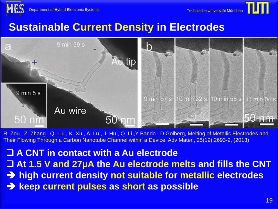
Sustainable Current Density in Electrodes
R. Zou , Z. Zhang , Q. Liu , K. Xu , A. Lu , J. Hu , Q. Li ,Y Bando , D Golberg, Melting of Metallic Electrodes and Their Flowing Through a Carbon Nanotube Channel within a Device. Adv Mater., 25(19),2693-9, (2013)
A CNT in contact with a Au electrode At 1.5 V and 27µA the Au electrode melts and fills the CNT high current density not suitable for metallic electrodes keep current pulses as short as possible

Technische Universität München Department of Hybrid Electronic Systems
Break junctions can be created in carbon structures operated in open systems (like in a TEM, vacuum probe station, even in air) if the critial current density is reached.
On/Off switching is observed in break junctions once a critical electric fields is achieved.
This can be explained by trapping of hydrocarbon gas between the junction and subsequent pyrolysis in a bad vacuum (10-7 mbar equals ~ 3·109 molecules/cm3).
Break junctions can also be created in porous carbon that is encapsulated.
Carbon structures separated by a short gap can be plumbed together by the application of an electric field. Joule heating from the field emission current will cause atom diffusion and rearrangement of carbon. Typical currents: 0.5 µA - 10 µA
20
Break-junctions and Plumbing in Carbon Structures

Technische Universität München Department of Hybrid Electronic Systems
21
Break-junctions and Plumbing in Graphenic C
B. Standley, W. Bao, H. Zhang, J. Bruck, C. N. Lau, M. Bockrath, Graphene-Based Atomic-Scale Switches, Nano Lett., Vol. 8, 13, 3345-3349, (2008)
Alexander Sinitskii, James M. Tour, Lithographic Graphitic Memories, ACS Nano Vol.3, No. 9, 2760–2766, (2009)
Technische Universität München Department of Hybrid Electronic Systems
22
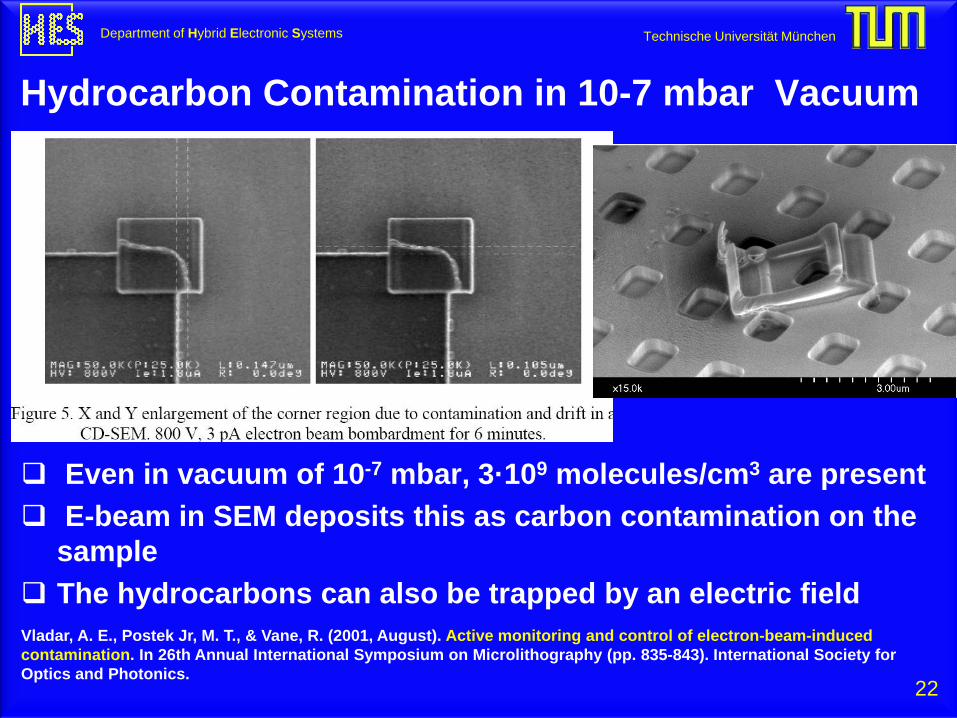
Hydrocarbon Contamination in 10-7 mbar Vacuum
Vladar, A. E., Postek Jr, M. T., & Vane, R. (2001, August). Active monitoring and control of electron-beam-induced contamination. In 26th Annual International Symposium on Microlithography (pp. 835-843). International Society for Optics and Photonics.
Even in vacuum of 10-7 mbar, 3·109 molecules/cm3 are present E-beam in SEM deposits this as carbon contamination on the
sample The hydrocarbons can also be trapped by an electric field

Technische Universität München Department of Hybrid Electronic Systems
23
Break-junctions and Plumbing in Graphenic C
Peter Ryan, Yu-ChiaoWu, Sivasubramanian Somu, George Adams, Nicol McGruer, Single-walled carbon nanotube electromechanical switching behavior with shoulder slip, J. Micromech. Microeng. 21, 045028, (2011)
Trapping of hydrocarbons debris in a CNT-switch upon the application of an electric field
Likely to be the main reason for on/off switching in open systems (TEM, vacuum probe station)

Technische Universität München Department of Hybrid Electronic Systems
24
Break-junctions and Plumbing in SW-CNTs
Chuanhong Jin, Kazu Suenaga, Sumio Iijima, Plumbing carbon nanotubes, Nature Nanotechnology 3, 17 - 21, (2008)
on-state off-state 12 uA
switch on 6 uA, 1.6V
on-state

Technische Universität München Department of Hybrid Electronic Systems
25
Break-junctions and Plumbing in CNTs
Koji Asaka, Motoyuki Karita, Yahachi Saito, Joining of multiwall carbon nanotubes for the end-contact configuration by applying electric current, Materials Letters 65,1832–1834, (2011)
When 1.0 V is applied between the MWNTs, the current increases to 15.6 μA and tips A and B coalesce at portions of the outermost wall layers

Technische Universität München Department of Hybrid Electronic Systems
26
Break-junctions and Plumbing in CNTs
Atsuko Nagataki, Takazumi Kawai, Yoshiyuki Miyamoto, Osamu Suekane, Yoshikazu Nakayama, Controlling Atomic Joints between Carbon Nanotubes by Electric Current, PRL 102, 176808, (2009)

Technische Universität München Department of Hybrid Electronic Systems
27
Break-junctions and Plumbing in Graphene
Rujia Zou, Zhenyu Zhang, Kaibing Xu, Lin Jiang, Qiwei Tian, Yangang Sun, Zhigang Chen, Junqing Hu, A method for joining individual graphene sheets, Carbon 50, 4965–4972, (2012)
" Under such high activation energy due to high current heating, the attaching edges of two opposite GSs undergo atoms’ activation, diffusion and reconstructing to rearrange the carbon networks, such as hexagonal rings, pentagon–heptagon pairs, for seamless joining"

Technische Universität München Department of Hybrid Electronic Systems
28
What Is Not Considered as Carbon-based Memory diffusing metal ions into insulating phases of carbon to
form a resistive memory effect based on metal filament creation and annihilation [36, 37, 38, 49]
metal diffusion occurs in almost all situations (like in ref. [37, 49]) where the capacitance discharge current from the first forming event is done by dc-voltage sweeps on samples with no on-chip current limiter, like on-chip resistors or transistors
SMU can neither limit the capacitance discharge current nor a dc-current on a time scale shorter than ~30 µs
also not considered: electronic memory effects in insulating forms of carbon films. The injected charge carriers modulate the tunnel barriers, but this is a volatile effect.

Technische Universität München Department of Hybrid Electronic Systems
29
Carbon-based Resistive Memory Phase Diagram
two different mechanism low mass density: break-junction by local evaporation of
carbon and plumbing by field emission high mass density: conversion of a-C ↔ sp2-bonds

Technische Universität München Department of Hybrid Electronic Systems
30
Field emission currents lead to rearrangement of the C-atoms and finally bridge the gap
sp2-bonds bridge a nano-gap in porous carbon (on-state). The sp2-bridge is deconstructed by a current pulse (~10 µA) Inherently scalable to atomic bonds
I2 > I1
high conductance low conductance
I1
Break-junctions and Plumbing in Porous Carbon

Technische Universität München Department of Hybrid Electronic Systems
31
sp2 to sp3 conversion of disordered graphitic carbon (phase change of carbon)
inherently scalable to atomic bonds (no phases of different materials)
sp3 sp2
I2 > I1
high conductance low conductance
I1
Amorphous Carbon to sp2-Bonds Conversion
sp3 bonds sp2 bonds sp2 bonds sp3 bonds

Technische Universität München Department of Hybrid Electronic Systems
32
First (!) current pulse needs to destroy all conducting paths The required current density (400 MA/cm2) is too high for high
mass density graphenic carbon Porous carbon might be accessible with ~10 MA/cm2
First Current Pulse Challenge with Conductive Carbon
after first pulse:
graphenic-C
porous-C

Technische Universität München Department of Hybrid Electronic Systems
33
Capacitance discharge currents (C*dV/dt) define Ron On-chip current limiter are needed (transistors) Forming voltage should be as low as possible
(tunable by C-thickness)
Forming Challenge with Insulating Carbon L. Dellmann, A. Sebastian, P. Jonnalagadda, C. A. Santini, W. W. Koelmans, C. Rossel, E. Eleftheriou, Nonvolatile resistive memory devices based on hydrogenated amorphous carbon, 43rd European Solid-State Device Research Conference (ESSDERC), (2013)

Technische Universität München Department of Hybrid Electronic Systems
34
My experience: cell RON is defined by first (forming) C*dV/dt That’s the reason why most ReRAM data have the same low RON, (<~ 20 kOhm) independent of the used material or stack Icap reduction techniques include on-chip current limiter and high temperature forming
Typical Cap-discharge Current (C*dV/dt)
Typical pad and probe tip have C > 1 pF
Speed is within rise time of the scopes
Relevant capacitance is within a sphere of r = t*vprop. <100ps*vprop. (Wahlgren – horizon picture)
Technische Universität München Department of Hybrid Electronic Systems
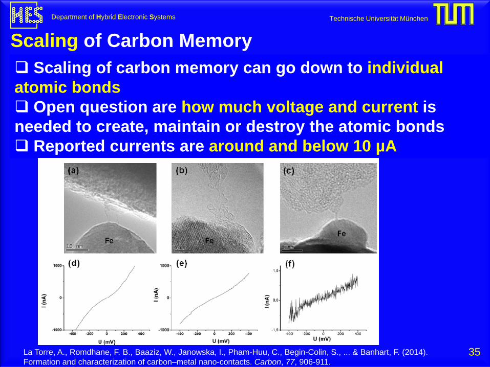
35
Scaling of carbon memory can go down to individual atomic bonds Open question are how much voltage and current is needed to create, maintain or destroy the atomic bonds Reported currents are around and below 10 µA
Scaling of Carbon Memory
La Torre, A., Romdhane, F. B., Baaziz, W., Janowska, I., Pham-Huu, C., Begin-Colin, S., ... & Banhart, F. (2014). Formation and characterization of carbon–metal nano-contacts. Carbon, 77, 906-911.

Technische Universität München Department of Hybrid Electronic Systems
36
Individual carbon chains show high resilience, but long time stability it is currently not known
Scaling of Carbon Memory: structural examples
Casillas, G., Mayoral, A., Liu, M., Ponce, A., Artyukhov, V. I., Yakobson, B. I., & Jose-Yacaman, M. (2014). New insights into the properties and interactions of carbon chains as revealed by HRTEM and DFT analysis. Carbon, 66, 436-441.
Technische Universität München Department of Hybrid Electronic Systems
37
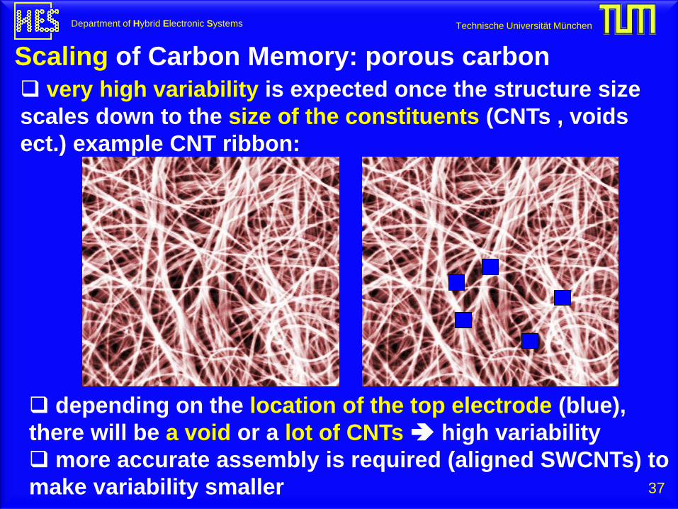
very high variability is expected once the structure size scales down to the size of the constituents (CNTs , voids ect.) example CNT ribbon:
Scaling of Carbon Memory: porous carbon
depending on the location of the top electrode (blue), there will be a void or a lot of CNTs high variability more accurate assembly is required (aligned SWCNTs) to make variability smaller

Technische Universität München Department of Hybrid Electronic Systems
38
Scaling of Carbon Memory: Contact Resistance
Biggest threat for scaling (ReRAM) might come from contact resistance Scales with area – what worked at ~100 nm, doesn't at ~10 nm! Associated voltage drop at high current densities is very high
J \ CR 1E-6 1E-7 5E-8
10 MA/cm2 10 V 1 V 0.5 V
1 MA/cm2 1 V 0.1 V 0.05 V
voltage drop at one contact:

Technische Universität München Department of Hybrid Electronic Systems
39
Architectural Challenges for Resistive Memories
In advanced nodes the interconnect wiring plays an active element due to IR-drop and RC-delay in wires & contacts Operating with fast pulses will be challenging or impossible A possible solution would be to operate the memory array in the capacitance discharge mode:
The interconnect wires are precharged to V by the x-access point while the y-access is still floating. After precharging, the x-access is is disconnected. The energy ½ CV2 that is stored in the interconnects is discharged to ground or even negative voltage by enabling the y-access. This approach guarantees that the wiring is discharged after the pulse and no set after reset can happen
x-access points for I, V control
y-access points for I, V control
cell IR-drop/RC-delay IR-drop/RC-delay

Technische Universität München Department of Hybrid Electronic Systems
40
Current State-Of-The Art For Carbon Memory Technology Fu, D., Xie, D., Feng, T., Zhang, C., Niu, J., Qian, H., & Liu, L. (2011). Unipolar resistive switching properties of diamondlike carbon-based RRAM devices. Electron Device Letters, IEEE, 32(6), 803-805
Only single cells This work has high capacitance layout Real time-resolved switching currents are not measured, but for set, at least an external current limiting resistor has been used Good data retention at 300°C for 600 min
Technische Universität München Department of Hybrid Electronic Systems
41
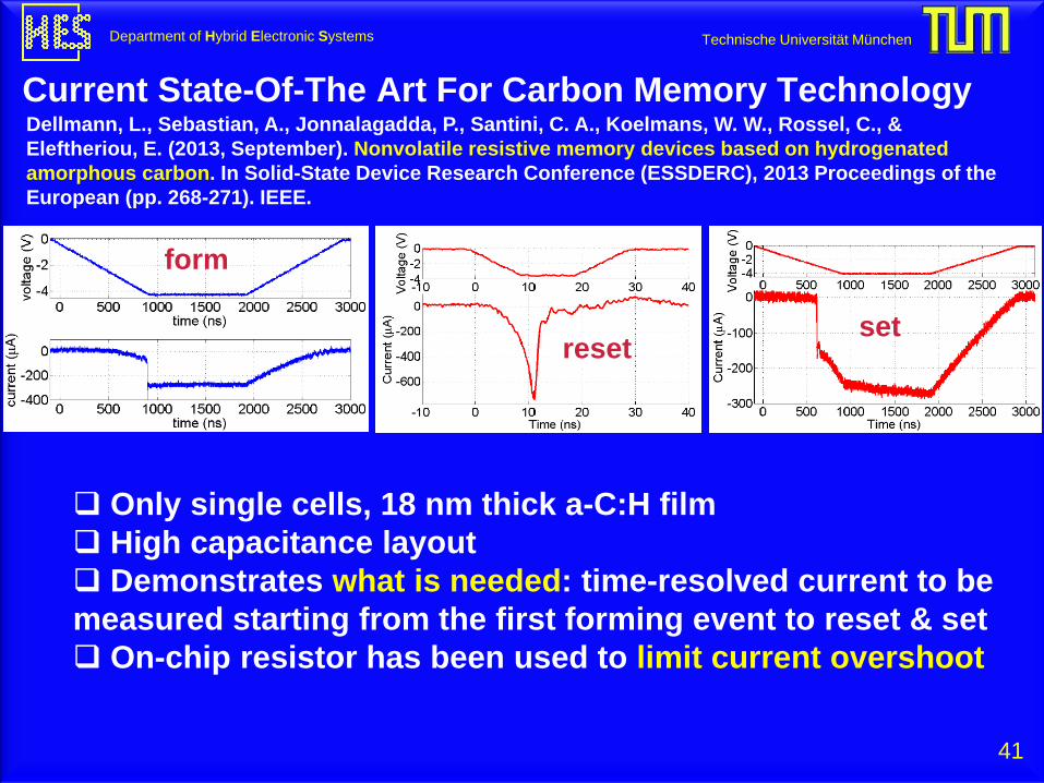
Current State-Of-The Art For Carbon Memory Technology Dellmann, L., Sebastian, A., Jonnalagadda, P., Santini, C. A., Koelmans, W. W., Rossel, C., & Eleftheriou, E. (2013, September). Nonvolatile resistive memory devices based on hydrogenated amorphous carbon. In Solid-State Device Research Conference (ESSDERC), 2013 Proceedings of the European (pp. 268-271). IEEE.
Only single cells, 18 nm thick a-C:H film High capacitance layout Demonstrates what is needed: time-resolved current to be measured starting from the first forming event to reset & set On-chip resistor has been used to limit current overshoot
form
reset set

Technische Universität München Department of Hybrid Electronic Systems
42
Current State-Of-The Art For Carbon Memory Technology The most advanced studies with results from 4 Mb arrays are based on porous CNT-ribbon memory from the company Nantero ( References [44, 45, 46, 47, 48])
4Mb arrays in 0.25 μm CMOS, some 20 nm cells are reported First pulse requirements are not reported and might be high 1011 endurance cycles on some cells with high capacitance layout are reported with 20 ns pulses (VLSI 2014) Switching currents vary and are estimated from gate voltage on huge transistor biased close to Vth (which have big variations) or are measured on individual cells to be in the order of 20-30 µA Overall, the published data are somewhat inconsistent (SEM shows 250 nm cell, text says 140 nm etc..)
Rosendale, Glen, et al. "A 4 Megabit Carbon Nanotube-based nonvolatile memory (NRAM)." ESSCIRC, 2010 Proceedings of the. IEEE, 2010.
Vread= 1 V
porous CNT ribbon film

Technische Universität München Department of Hybrid Electronic Systems
43
Challenge of Predicting Technology Performance Real Chip layout and technology are needed But these are proprietary data, which are not disclosed Example: well-known DRAM chips run same task, same JEDEC specs, different vendors and technologies
Even idle currents are 3x different!

Technische Universität München Department of Hybrid Electronic Systems
44
Appendix 1: Metrics for memory device assessment
Description
Unobtainable-RAM
(e.g., “Ideally…”) CARBON MEMORY
Comments
(including any associated tradeoffs)
Scal
abili
ty, s
ize,
cos
t
Scalability Each layer @ 4F2
down to beyond 12nm node
@ 4F2 down to single atomic bonds
both memory cell AND wire pitch can be scaled. But care needs to be taken about the select device. Major threat comes from contact resistances
Multi-level cells (MLC)
Up to 3bits/cell 2 bits/cell are demonstrated [48], Recommended is 1bits/cell
MLC in RRAM is possible for relaxed feature sizes. IF RC from interconnects play an important role only, Ron > 200 kOhm might be accessible
Multi-layer stacking
At least 32 layers 8-12 Multilayer might be possible
BEOL compatibility depends on the select device. Complicated stacks needs to be etched at 8-12 layer. 3D monolithic integration might be feasible
Fabrication costs
Total cost very similar to current NAND or lower
Similar to PCM or RRAM
Number of critical mask steps= 1 for 1layer CMOS - No new/difficult unit processes -New/difficult materials only with nanotubes, a-C is known to be compatible with CMOS processing- device forming is necessary (first pulse challenge)!
Array efficiency
>100% (circuitry tucked underneath, w/ extra Si real-estate left over)
Similar to PCM or RRAM
• BL/WL lengths • Extent of peripheral circuitry • Peripheral circuitry play a critical role (such as compliance, or current limiting needed for low power • Interplay with 3D stacking

Technische Universität München Department of Hybrid Electronic Systems
45
Appendix 1: Metrics for memory device assessment
Description
Unobtainable-RAM
(e.g., “Ideally…”) CARBON MEMORY
Comments
(including any associated tradeoffs)
Stat
e-of
-the
-ar
t
Array size N/A (Unobtaina-RAM has not been demonstrated)
4 Mbit [45] obtained individually…
Yield N/A Not known
Technology node
N/A 20 nm cells demonstrated (in public domain) [45]
But not for both the implemented CMOS device AND for the wiring pitch (CMOS 0.25 µm) First current pulse issue not investigated
Late
ncy
(Bot
h ce
ll-le
vel a
nd
syst
em-le
vel,
if kn
own)
Read latency
< 10ns (for memory applications) (~1us for storage applications)
~50 ns for 1 [45] ~30 ns for 0 [45]
• read contrast ~1000 • Size of read window • Read disturb issues • Errors from crosstalk = all depend on chip design
Write latency
< 20ns (for memory applications) ~1us for storage applications)
~20 ns [48] • Requires verify-after-write/erase • Write disturb of other devices = research • Damage threshold to avoid? = research • write-in-place supported = all depend on chip design

Technische Universität München Department of Hybrid Electronic Systems
46
Appendix 1: Metrics for memory device assessment
Description
Unobtainable-RAM
(e.g., “Ideally…”) CARBON MEMORY
Comments
(including any associated tradeoffs)
Pow
er /
Ene
rgy
Read power / Energy
< 1/10 scaled DRAM for memory applications
(for storage applications, same as scaled NAND or better)
1V/10 nA 1V/10µA
Power parallelism bandwidth Roadmap with scaling Please specify power usage… • …by selected devices • …elsewhere in the array (leakage, line
resistances), and • …in peripheral circuitry
= depends on proprietary chip design…
Write power / Energy
for memory applications,
< 1/5 scaled DRAM (for storage applications, <5x read power)
15pJ/bit [48] Power parallelism bandwidth Roadmap with scaling? power usage… • …by selected devices • …elsewhere in the array (leakage, line
resistances), and • …in peripheral circuitry
= depends on proprietary chip design…

Technische Universität München Department of Hybrid Electronic Systems
47
Appendix 1: Metrics for memory device assessment
Description
Unobtainable-RAM
(e.g., “Ideally…”) CARBON MEMORY
Comments
(including any associated tradeoffs)
Relia
bilit
y
Endurance >>1e12 (memory applications)
(>1e9, storage applications)
>1e11 [48] • Can device failures be predicted = research subject, scales with node… • Devices fail to what state? = research subject, scales with node… • Do failed devices affect neighbors? = research subject, depends on design • Impact on other characteristics? (e.g., do cycled devices behave differently?) =research subject, scales with node… • Are failures random or clustered? = research subject, scales with node…
Retention >1 month @ 85oC (memory) >10 years @ 150oC (storage)
>10 years @ 120oC 300 min @ 300 C [41] 168 h @ 250 C [44]
tradeoffs, between retention & write-speed, or retention & cycling? = research subject, scales with node…
Variability Extremely low (e.g., 6th-sigma device also meets all specs)
If we would have 6 sigma, we would have a product….
Intra-device & inter-device – variability & repeatability? = research subject, scales with node… Porous carbon will have a problem at small dimension

Technische Universität München Department of Hybrid Electronic Systems
Selected Literature
48
[1] Kyu Hun Kim, Youngseok Oh and M. F. Islam, Graphene coating makes carbon nanotube aerogels superelastic and resistant to fatigue, Nature Nanotechnology 7, 562–566, (2012). [2] Shunsuke Sakurai, Fuminori Kamada, Don N. Futaba, Motoo Yumura and Kenji Hata, Influence of lengths of millimeter-scale single-walled carbon nanotube on electrical and mechanical properties of buckypaper, Nanoscale Res Lett.; 8(1): 546, ( 2013). [3] Luciano Colombo, Annalisa Fasolino (Eds.), Carbon Materials: Chemistry and Physics, Vol.3, Computer-Based Modeling of Novel Carbon Systems and Their Properties: Beyond Nanotubes, Springer, 250 p.,( 2010). [4] Florian Banhart, Irradiation effects in carbon nanostructures, Rep. Prog. Phys. 62 1181–1221, (1999). [5] Amelia Barreiro, Felix Börrnert, Stanislav M. Avdoshenko, Bernd Rellinghaus, Gianaurelio Cuniberti, Mark H. Rümmeli, Lieven M. K. Vandersypen, Understanding the catalyst-free transformation of amorphous carbon into graphene by current-induced annealing, Scientific Reports, 3: 1115, (2013). [6] J. Y. Huang, S. Chen, Z. F. Ren, G. Chen and M. S. Dresselhaus, Real-Time Observation of Tubule Formation from Amorphous Carbon Nanowires under High-Bias Joule Heating, Nano Letters, Vol. 6, No. 8,1699-1705 (2006) [7] M. B. Agranat, S. I. Ashitkov, A. V. Kirillin, A. V. Kostanovskii, V. E. Fortov, S. I. Anisimov, P. S. Kondratenko, Formation of amorphous carbon on melting of microcrystalline graphite by picosecond laser pulses, Journal of Experimental and Theoretical Physics Letters, Vol. 66, 10, pp 699-703,(1997). [8] G. Vitali, M. Rossi, M. L. Terranova, and V. Sessa, Laserinduced structural modifications of glassy carbon surfaces, J. Appl. Phys. 77, 4307 (1995). [9] R. Gago, M. Vinnichenko, H. U. Jäger, A. Yu. Belov, I. Jiménez, N. Huang, H. Sun, and M. F. Maitz, Evolution of sp2 networks with substrate temperature in amorphous carbon films: Experiment and theory, Phys. Rev. B 72, 014120 (2005). [10] J. O. Orwa, I. Andrienko, J. L. Peng, S. Prawer, Y. B. Zhang, and S. P. Lau, Thermally induced sp-2 clustering in tetrahedral amorphous carbon (ta-C) films, Journal of Applied Physics 96, 6286 (2004). [11] D. W. M. Lau, D. G. McCulloch, M. B. Taylor, J. G. Partridge, D. R. McKenzie, N. A. Marks, E. H. T. Teo, and B. K. Tay, Abrupt Stress Induced Transformation in Amorphous Carbon Films with a Highly Conductive Transition Phase, Phys. Rev. Lett., 100, 176101, (2008). [12] J. Y. Huang, In Situ Observation of Quasimelting of Diamond and Reversible Graphite−Diamond Phase Transformations, Nano Lett. Vol. 7, No. 8, 2335-2340 (2007). [13] Jin Gyu Park, Shu Li, Richard Liang, Chuck Zhang, Ben Wang, Structural changes and Raman analysis of single-walled carbon nanotube buckypaper after high current density induced burning, Carbon 46, 1175 – 1183, (2008). [14] F. Kreupl, R. Bruchhaus, P. Majewski , J. B. Philipp, R. Symanczyk, T. Happ,.C. Arndt, M. Vogt, R. Zimmermann, A. Buerke, A. P. Graham, M. Kund, Carbon-Based Resistive Memory, Proceedings of the IEDM, 521, (2008). [15] F. Kreupl, Carbon-based Materials as Key-enabler for More Than Moore, MRS Proceedings Vol. 1303, pp. 1 – 13, (2011). [16] H.Li, C. C. Russ, Wei Liu, D. Johnsson, H. Gossner and K. Banerjee, On the Electrostatic-Discharge Robustness of Graphene, IEEE TED, Vol. 61, No. 6, pp. 1920-1928, (2014).

Technische Universität München Department of Hybrid Electronic Systems
Selected Literature
49
[17] T. D. Yuzvinsky, W. Mickelson, S. Aloni, S. L. Konsek, A. M. Fennimore, G. E. Begtrup, A. Kis, B. C. Regan, and A. Zettl, Imaging the life story of nanotube devices, APL 87, 083103, (2005). [18] R. Zou , Z. Zhang , Q. Liu , K. Xu , A. Lu , J. Hu , Q. Li ,Y Bando , D Golberg, Melting of Metallic Electrodes and Their Flowing Through a Carbon Nanotube Channel within a Device. Adv Mater., 25(19),2693-9, (2013). [19] X. Jiang, W. Beyer, and K. Reichelt, Gas evolution from hydrogenated amorphous carbon films, APL. ,68, 1378, (1990). [20] B. Standley, W. Bao, H. Zhang, J. Bruck, C. N. Lau, M. Bockrath, Graphene-Based Atomic-Scale Switches, Nano Lett., Vol. 8, 13, 3345-3349, (2008). [21] Hang Zhang, Wenzhong Bao, Zeng Zhao, Jhao-Wun Huang, Brian Standley, Gang Liu, Fenglin Wang, Philip Kratz, Lei Jing, Marc Bockrath,, Chun Ning Lau, Visualizing Electrical Breakdown and ON/OFF States in Electrically Switchable Suspended Graphene Break Junctions, Nano Lett. 12, 1772−1775, (2012). [22] Yubao Li, Alexander Sinitskii, James M. Tour, Electronic two-terminal bistable graphitic memories, Nature Materials 7, 966 - 971 (2008). [23] A. Sinitskii, James M. Tour, Lithographic Graphitic Memories, ACS Nano Vol.3, No. 9, 2760–2766, (2009). [24] Paulo Araujo, Albert Liao, Joaquin Rodriguez-Nieva, Eduardo Barros, Hyun Jung, Ji Hao, Yung Jung, Mildred Dresselhaus, Carbon Nanotube Network Anti-fuses, Bulletin of the American Physical Society, 59, (2014). [25] Michael T. Postek, An Approach to the Reduction of Hydrocarbon Contamination in the Scanning Electron Microscope, Scanning Vol. 18, 269–274 (1996). [26] Peter Ryan, Yu-ChiaoWu, Sivasubramanian Somu, George Adams, Nicol McGruer, Single-walled carbon nanotube electromechanical switching behavior with shoulder slip, J. Micromech. Microeng. 21, 045028, (2011). [27] Chuanhong Jin, Kazu Suenaga, Sumio Iijima, Plumbing carbon nanotubes, Nature Nanotechnology 3, 17 - 21, (2008). [28] Koji Asaka, Motoyuki Karita, Yahachi Saito, Joining of multiwall carbon nanotubes for the end-contact configuration by applying electric current, Materials Letters 65,1832–1834, (2011). [29] Atsuko Nagataki, Takazumi Kawai, Yoshiyuki Miyamoto, Osamu Suekane, Yoshikazu Nakayama, Controlling Atomic Joints between Carbon Nanotubes by Electric Current, PRL 102, 176808, (2009). [30] Rujia Zou, Zhenyu Zhang, Kaibing Xu, Lin Jiang, Qiwei Tian, Yangang Sun, Zhigang Chen, Junqing Hu, A method for joining individual graphene sheets, Carbon 50, 4965–4972, (2012). [31] Ovidiu Cretu, Andreś R. Botello-Mendez, Izabela Janowska, Cuong Pham-Huu, Jean-Christophe Charlier, Florian Banhart, Electrical Transport Measured in Atomic Carbon Chains, Nano Lett. 13, 3487−3493, (2013). [32] Zhen Xu , Zheng Liu , Haiyan Sun , Chao Gao, Highly Electrically Conductive Ag-Doped Graphene Fibers as Stretchable Conductors, Adv. Mater., 25, 3249–3253, (2013). [33] in Gyu Park, Shu Li, Richard Liang, Xinyu Fan, Chuck Zhang, Ben Wang, The high current-carrying capacity of various carbon nanotube-based buckypapers, Nanotechnology 19, 185710, (2008).

Technische Universität München Department of Hybrid Electronic Systems
Selected Literature
50
[35] C. S. Yoo and W. J. Nellis, Phase Transformations in Carbon Fullerenes at High Shock Pressures, Science, Vol. 254, No. 5037, pp. 1489-1491, (1991). [36] F. Zhuge, W. Dai, C. L. He, A. Y. Wang, Y. W. Liu, M. Li, Y. H. Wu, P. Cui, Run-Wei Li, Nonvolatile resistive switching memory based on amorphous carbon, Applied Physics Letters 96, 163505, (2010). [37] Yi-Jiun Chen, Hsin-Lu Chen, Tai-Fa Young, Ting-Chang Chang, Tsung-Ming Tsai, Kuan-Chang Chang, Rui Zhang, Kai-Huang Chen, Jen-Chung Lou, Tian-Jian Chu, Jung-Hui Chen, Ding-Hua Bao, Simon M Sze, Hydrogen induced redox mechanism in amorphous carbon resistive random access memory, Nanoscale Research Letters, 9:52, (2014). [38] Yang Chai, Yi Wu, Kuniharu Takei, Hong-Yu Chen, , Shimeng Yu, Philip C. H. Chan, Ali Javey, H.-S. Philip Wong, Nanoscale Bipolar and Complementary Resistive Switching Memory Based on Amorphous Carbon, IEEE TED Vol. 58, No. 11, (2011). [39] L. Dellmann, A. Sebastian, P. Jonnalagadda, C. A. Santini, W. W. Koelmans, C. Rossel, E. Eleftheriou, Nonvolatile resistive memory devices based on hydrogenated amorphous carbon, 43rd European Solid-State Device Research Conference (ESSDERC), (2013). [40] Jianlong Xu, Dan Xie, Tingting Feng, Chenhui Zhang, Xiaowen Zhang, Pinggang Peng, Di Fu, He Qian, Tian-ling Ren, Litian Liu, Scaling-down characteristics of nanoscale diamond-like carbon based resistive switching memories, Carbon 75, 255–261, (2014). [41] Di Fu, Dan Xie, Tingting Feng, Chenhui Zhang, Jiebin Niu, He Qian, and Litian Liu, Unipolar Resistive Switching Properties of Diamondlike Carbon-Based RRAM Devices, IEEE Electron Device Letters, Vol. 32, No. 6, (2011). [42] Alessandro La Torre, Ferdaous Ben Romdhane, Walid Baaziz, Izabela Janowska, Cuong Pham-Huu, Sylvie Begin-Colin, Genevie`ve Pourroy, Florian Banhart, Formation and characterization of carbon–metal nano-contacts, Carbon 77, 906–911, (2014). [43] Gilberto Casillas, Alvaro Mayoral, Mingjie Liu, Arturo Ponce, Vasilii I. Artyukhov, Boris I. Yakobson, Miguel Jose-Yacaman, New insights into the properties and interactions of carbon chains as revealed by HRTEM and DFT analysis, Carbon 66, 436–411, (2014). [44] R.F. Smith, T.Rueckes, S. Konsek, J.W. Ward, D.K. Brock, and B.M. Segal, Carbon Nanotube Based Memory Development and Testing, EEEAC paper #1310, (2006). [45] Glen Rosendale, Sohrab Kianian, Monte Manning, Darlene Hamilton, X.M. Henry Huang, Karl Robinson, Young Weon Kim, Thomas Rueckes, A 4 Megabit Carbon Nanotube-based Nonvolatile Memory (NRAM), Proceedings of the ESSCIRC, (2010). [46] Sohrab Kianian, Glen Rosendale, Monte Manning, Darlene Hamilton, X. M. Henry Huang, Karl Robinson, Young Weon Kim, Thomas Rueckes, A 3D Stackable Carbon Nanotube-based Nonvolatile Memory (NRAM), Proceedings of the ESSDERC, (2010). [47] Glen Rosendale, Darlene Viviani, Monte Manning, X.M. Henry Huang, ShiJie Wen, Richard Wong, Thomas Rueckes, Storage Element Scaling Impact on CNT Memory Retention and On/Off Window, IEEE 6th International Memory Workshop (IMW), (2014). [48] Sheyang Ning, Tomoko Ogura Iwasaki, Kazuya Shimomura, Koh Johguchi, Glen Rosendale, Monte Manning, Darlene Viviani, Thomas Rueckes, Ken Takeuchi, 23% Faster Program and 40% Energy Reduction of Carbon Nanotube Non-volatile Memory with Over 1011 Endurance, VLSI Technology Symposium 2014 [49] Pinggang Peng, Dan Xie, Yi Yang, Yongyuan Zang, Xili Gao, Changjian Zhou, Tingting Feng, He Tian, Tianling Ren, and Xiaozhong Zhang, Resistive switching behavior in diamond-like carbon films grown by pulsed laser deposition for resistance switching random access memory application, JAP 111, 084501 (2012)

Technische Universität München Department of Hybrid Electronic Systems
51
Electrode Diffusion: A Consequence of High Current Density
Demolliens, A., Muller, C., Deleruyelle, D., Spiga, S., Cianci, E., Fanciulli, M., ... & Ielmini, D. (2009, May). Reliability of NiO-based resistive switching memory (ReRAM) elements with pillar W bottom electrode. In Memory Workshop, 2009. IMW'09. IEEE International (pp. 1-3). IEEE.