FPGA Implementation of UTMI and Protocol Layer for …ethesis.nitrkl.ac.in/4979/1/109EC0222.pdf ·...
57
i A PROJECT REPORT (THESIS) ON FPGA IMPLEMENTATION OF UTMI AND PROTOCOL LAYER FOR USB 2.0 By SWARUP KUMAR MAHAPATRA 109EC0222 SADHNA MUANKHIA 109EC0224 Under the Guidance of Prof. A.K. SWAIN Department of Electronics & Communication Engineering National Institute of Technology, Rourkela- 769008 2012-13
Transcript of FPGA Implementation of UTMI and Protocol Layer for …ethesis.nitrkl.ac.in/4979/1/109EC0222.pdf ·...

i
A PROJECT REPORT (THESIS)
ON
FPGA IMPLEMENTATION OF UTMI
AND PROTOCOL LAYER FOR USB 2.0
By
SWARUP KUMAR MAHAPATRA
109EC0222
SADHNA MUANKHIA
109EC0224
Under the Guidance of
Prof. A.K. SWAIN
Department of Electronics & Communication Engineering
National Institute of Technology,
Rourkela- 769008
2012-13

ii
National Institute of Technology, Rourkela
CERTIFICATE
This is to certify that the thesis entitled, “FPGA IMPLEMENTATION OF UTMI AND
PROTOCOL LAYER OF USB 2.0” submitted by SWARUP KUMAR MAHAPATRA
(109EC0222) and SADHNA MUANKHIA (109EC0224) in partial fulfillment of the
requirements for the award of Bachelor of Technology degree in Electronics and
Communication Engineering during the session 2012-13 at National Institute of
Technology, Rourkela (Deemed University) and is a bonafied work done by them under my
supervision and guidance.
To the best of my knowledge, the matter embodied in the thesis has not been
submitted to any other university/institute for the award of any Degree/Diploma.
Date Prof A. K. Swain
Department of Electronics and Communication
National Institute of Technology
Rourkela-769008

iii
ACKNOWLEDGEMENT
We would like to express our gratitude to my thesis guide Prof A. K. Swain for his guidance
and consistent support throughout the time-span of this Project work.
We would also like to thank Prof K.K. Mahapatra, Prof D. P. Acharya and Prof S. K.
Patra for taking up the courses of Digital VLSI Design, Embedded Systems and
Microprocessors respectively which inspired us to take up this project which comes under the
category VLSI and Embedded system.
We would like to thank the VLSI lab staffs for providing us the adequate materials, kits and
software which were essential for developing our project.
Lastly we would like to thank the Institute for giving us the opportunity to study here and
enrich our knowledge and skills and providing us the state-of-art infrastructure.
Swarup Kumar Mahapatra
Roll No: 109EC0222
Sadhna Muankhia
Roll No: 109EC0224

iv
CONTENTS
Acknowledgement ……………………………………………………………………… iii
List of figures and tables……………………………………………………………….... vi
Abstract…………………………………………………………………………………..vii
Chapter 1: OVERVIEW………………………………………………………………….. 1
1.1 INTRODUCTION…………………………………………………………... . 2
1.2 USB BACKGROUND………………………………………………………. 2
1.3 PROBLEM STATEMENT…………………………………………………... 3
1.4 IMPLEMENTATION TOOLS……………………………………………… 4
Chapter 2: SPECIFICATIONS………………………………………………………….. 6
2.1 SYSTEM DESCRIPTION…………………………………………………... 7
2.2 COMMUNICATION FLOW...................................................…..................... 9
2.3 HOST-DEVICE COMMUNICATION…………………………………..... . 11
2.4 PACKET DESCRIPTION............................................................................... 14
Chapter 3: DESIGN ARCHITECTURE........................................................................... 19
3.1 GENERAL ARCHITECTURE....................................................................... 20
3.2 UTMI INTRODUCTION................................................................................ 22
3.3 UTMI SIGNAL DESCTIPTION..................................................................... 23
3.4 UTMI BLOCK LEVEL DESCRIPTION........................................................ 26
3.5 PROTOCOL LAYER...................................................................................... 33
3.6 PROTOCOL ENGINE.................................................................................... 37

v
Chapter 4: SIMULATIONS AND RESULT.................................................................. 39
4.1 UTMI SIGNALS SIMULATION................................................................. 40
4.2 PACKET ASSEMBLY SIMULATION....................................................... 41
4.3 PACKET DISASSEMBLY SIMULATION................................................ 42
4.4 DATA BUFFERIG SIMULATION............................................................. 43
4.5 PROTOCOL ENGINE SIMULATION........................................................ 44
Chapter 5: CONCLUSION............................................................................................. 46
Chapter 6: FUTURE WORK.......................................................................................... 48

vi
LIST OF FIGURES
Figure 1.1 Spartan 3E FPGA board.................................................................................. 5
Figure 2.1 USB Bus Topology.......................................................................................... 8
Figure 2.2 Host-Device communication model................................................................ 9
Figure 2.3 Implementation Areas.................................................................................... 10
Figure 2.4 Endpoint Communication Flow..................................................................... 12
Figure 3.1 USB Core architecture................................................................................... 20
Figure 3.2 Memory Interface and Arbiter ...................................................................... 21
Figure 3.3 UTMI block level diagram............................................................................ 26
Figure 3.4 FS CLK relations to Receive/Transmit data and Control signals................ 27
Figure 3.5 Rx Shift/Hold Register.................................................................................. 28
Figure 3.6 Receive state machine................................................................................... 29
Figure 3.7 Receive timing cycle..................................................................................... 29
Figure 3.8 Tx Shift/Hold Register................................................................................... 31
Figure 3.9 Transmit state machine.................................................................................. 31
Figure 3.10 Transmit timing cycle ................................................................................. 31
Figure 3.11 Protocol Layer overview ............................................................................ 33
Figure 4.1 UTMI waveform ........................................................................................... 40
Figure 4.2 Packet Assembly waveform.......................................................................... 41
Figure 4.3 Packet Disassembly waveform...................................................................... 42
Figure 4.4 Data Buffering waveform.............................................................................. 43
Figure 4.5 USB core main flow chart............................................................................. 44
Figure 4.6 IN Cycle ...................................................................................................... 44
Figure 4.7 OUT cycle .................................................................................................... 44
Figure 4.8 Protocol Engine waveform ........................................................................... 45
LIST OF FIGURES
Table 2.1 Packet Identifier (PID) description table ..................................................... 15
Table 2.2 Token packet format .................................................................................... 17
Table 2.3 Data packet format ...................................................................................... 18
Table 2.4 Handshake packet format ............................................................................ 18
Table 2.5 Start of Frame (SOF) packet format ............................................................ 18
Table 3.1 Control Status Register bit definition .......................................................... 36

vii
ABSTRACT
With the advancement in hardware technology, FPGA coming into existence are able to
accommodate faster and more powerful electronic devices on a single device.
IP Cores have been developed to enable design reuse, increasing functionality, performance
and flexibility.
USB is a serial bus which can realize the Plug and Play feature for easy connection of
peripherals to PCs. It is a point to point interface in which data rate of over 480Mbit/s can be
transferred as per new USB 2.0 Specification. It provides bi-directional, low- cost and high
speed serial interface for data transfer. Multiple devices can be attached through a hub to the
host. The USB Communication implemented complies with USB 2.0 Specifications essential
for basic data transfer and can operate at USB Full speed (12 Mbit/s) and High speed
(480Mbit/s).
This project deals with implementation of a USB Core specifically UTMI and protocol layer
module on FPGA. The design is done by writing code in verilog HDL which is then verified
and synthesized using Xilinx XST. The result is verified using testbench waveform to study
the transactions carried out by USB and how packet serialization and de-serialization, error
checking is done.

1
Chapter 1
OVERVIEW

2
1.1 INTRODUCTION
The Universal Serial Bus is a standard communication interface developed for
interconnection between computer and peripheral devices. The peripherals include pointing
devices, keyboard, printers, digital cameras, etc. The bus supports the plug and play feature.
This implies that there is no need to open up the PC while adding a new device and allowing
the software to get installed automatically. It provides low cost, bi- directional and high speed
data transfer. Using USB 2.0 specification, data rate of 480Mbps transmission can be carried
out. It is a point to point interface. Multiple devices can be attached from host to hub. The
main aim of the USB protocol was to reduce the number of ports for PC connectivity.
1.2 USB BACKGROUND
USB was developed by a group of seven companies namely COMPAQ, IBM, INTEL,
MISCROSOFT, DEC, NEC and NORTEL in the year 1994.Though the USB 1.0
specification was developed in January 1996 which produced data rates of 1.5Mbit/s (LOW
SPEED) and 12 Mbit/s (HIGH SPEED) [3]
, the widely used version was 1.1 released in
September 1998.
The later version, USB 2.0 was released in April 2000. The companied Hewlett-Packard,
Alcatel Lucent, Philips and above mentioned firms took a joint initiative so as to generate a
high data transfer rate of 480Mbit/s.
A supplement release of USB-On-The-Go specification was carried out in December 2006.
This specification enabled two USB devices to communicate with each other without the
need of a separate USB host.
The latest release is USB 3.0, released in November 2008 and had the objectives to increase
the data rate and reduce the power consumption as well as to increase the output power.

3
1.3 PROBLEM STATEMENT
The USB high speed cores have already been implemented by many companies. But these
companies protect their secrets and patents due the efforts and time spend in the development
of the cores. Usually the user download the code from the net for trial simulation and if they
are satisfied with the code, then a license fee is paid to purchase a key which allow us the
programming of the device. But the problem comes in the affordability of the users as the
cores are expensive to purchase.
The rise of FPGA boards in the market and its ease of availability in the labs can help to
develop our own USB host IP core. The FPGA have their own USB ports which will
communicate only if the cores are run on the FPGA.
The users have a very little idea the Packet forms used in the communication between the
host and device. Hence we need to implement the hardware design of the Host that
implements the USB protocol.
We expect our Final Year Project will help to develop a student research based; non-
commercial IP core that implements a USB host and this host can be used by further
generations to develop more advanced cores.

4
1.4 IMPLEMTATION TOOLS
Several developmental tools were used for the implementation of our project. This includes
generating Test-bench waveform, RTL simulations etc. and design summary.
We used Xilinx ISE (integrated software environment) 10.1 software for designing out circuit
using Verilog code and Developing the Test-bench and schematics of the modules.
This software allows us to take our design from design entry through Xilinx device
programming. The ISE project navigator processes our design through various steps in the
ISE design flow.
The following are the steps used
Design Entry
Synthesis
Implementation
Simulation and verification
Device Configuration
The Test-bench waveform containing the signals can be used to simulate the modules used in
our project in the Xilinx ISE simulator.
The hardware implementation was done using Spartan 3E starter kit. This provides a
powerful and highly advanced self-contained development platform for designs targeting the
Spartan 3e FPGA from Xilinx. Features like Xilinx Platform Flash, USB end, JTAG parallel
programming interfaces are also found on this board.

5
Figure 1.1 Spartan 3E FPGA board
[10]
Spartan 3E Starter Board details IC Xilinx Spartan 3E FPGA (500K gates)
Connector 100-pin Hirose FX2 connector
Three 6-pin Pmod connectors
DB15HD VGA
PS/2 keyboard
Two DB9 RS-232 connectors
RJ-45 Ethernet
16-pin header for optional LCD modules
SMA connector
Programming: JTAG programming through on-board USB2 port; JTAG & SPI
Flash programming with parallel or USB JTAG Cable; numerous
additional configuration options

6
Chapter 2
SPECIFICATIONS

7
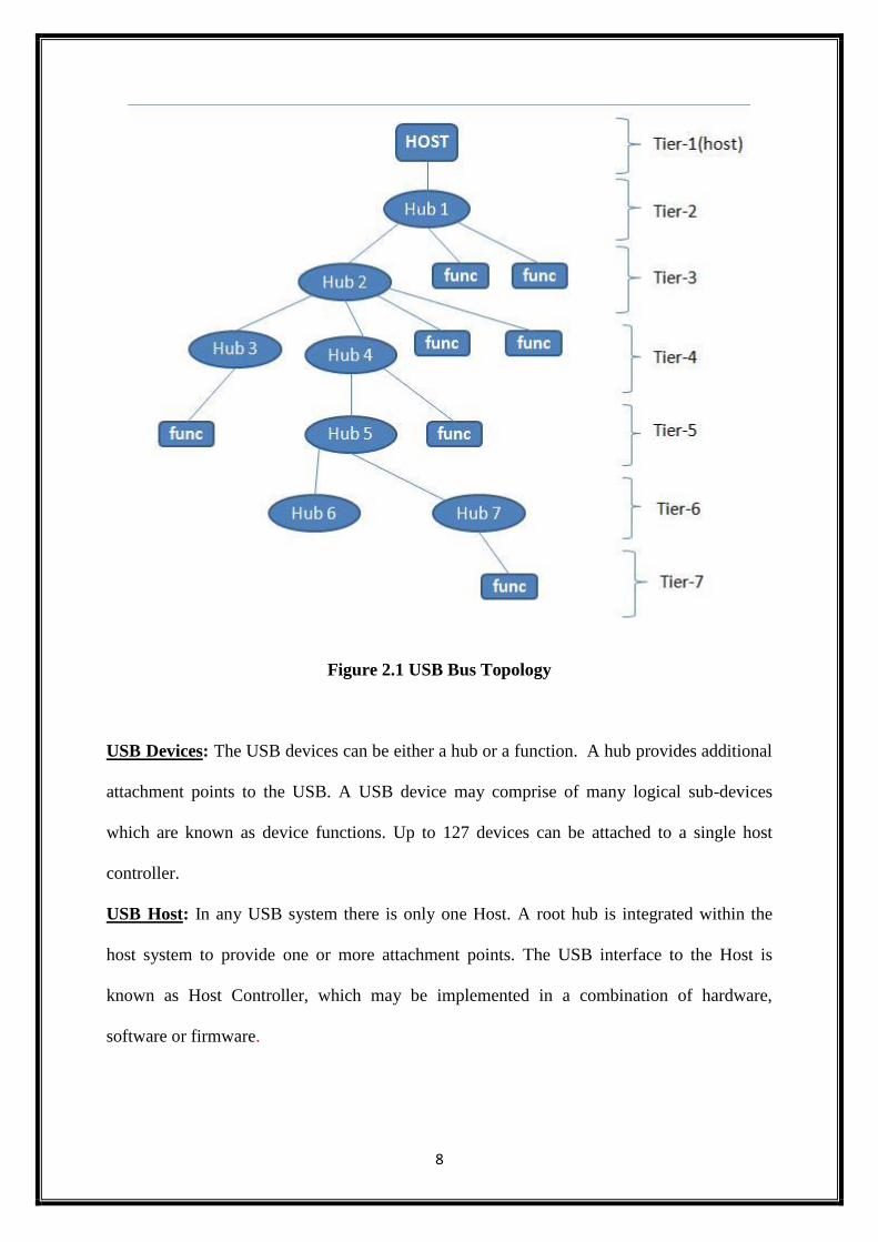
2.1 SYSTEM DESCRIPTION
A USB system has the following intrinsic areas
USB interconnect
USB devices
USB host
USB interconnect: It describes the manner in which the USB devices are connected and
communicates with the attached host. This includes
Bus topology: The connection model between Host and USB devices
Inter-layer Relationships: In terms of stack capability, the USB tasks are performed
at each layer in the system.
Data Flow Models: It is the manner in which data traverses in the system over the
USB between producers and consumers.
USB Schedule: The USB provides a shared interconnect. The access to the
interconnect are scheduled so as to support isochronous data transfers and to
eliminate arbitration overhead.
Bus topology: It follows a tier-star topology in which the Hub is at the center of each star and
there is a point to point connection between host and hub /function or hub connected to
hub/function. The maximum number of tiers allowed is 7 including the root hub.
Each compound device covers two tiers; hence it can’t be enabled if it is attached at tier-7.
This is because only functions can be enabled at tier-7.
8
Figure 2.1 USB Bus Topology
USB Devices: The USB devices can be either a hub or a function. A hub provides additional
attachment points to the USB. A USB device may comprise of many logical sub-devices
which are known as device functions. Up to 127 devices can be attached to a single host
controller.
USB Host: In any USB system there is only one Host. A root hub is integrated within the
host system to provide one or more attachment points. The USB interface to the Host is
known as Host Controller, which may be implemented in a combination of hardware,
software or firmware.

9
2.2 COMMUNICATION FLOW
The USB cable serves as the communication path between the attached USB device and the
host. The host has 3 distinct layers as shown in the figure below. Similarly the device
attached to the host has 3 layers. The physical communication takes place through the lower
most layers i.e. the USB wire. There is Logical communication between the host and the
device above the physical layer
Figure 2.2 Host-Device communication model
For the purpose of our project we tried to implement few portions of the host side. The
further discussions will be on the layers to the left of the above figure. The dark horizontal
arrow shows the physical connectivity between the host and the device whereas the light
horizontal allow shows the logical inter-layer connectivity among the host and device. The
vertical arrow shows the intra host and intra device layers connectivity.
The figure in the next page gives more detail about the different layers of a USB host.

10
Figure 2.3 Implementation Areas[3]
We mostly focused on the lowermost physical layer (in blue highlights) which accepts data
from the level above and send in the bits to the USB cable. We expect in future the Host
Controller Driver code would be written in C, and the hardware would be tested. The
software interface is completely dependent on the hardware implementation and need not
follow any USB driver specification. The Software layer collects the details of the protocols
that are implemented in the hardware layer. The Software layer is involved in managing
transactions whereas the physical layer is involved in managing packets and bits. The
topmost layer is the Client Software Layer, typically in ‘C’ code, interacts with the USB
device using high level functions like write_USB( ) and read_USB( ). The Client layer was
not implemented as well in our Project.

11
Physical Layer
The Physical Layer, also known as USB Bus interface Layer, handles the communication of
raw data bits upon the USB wire. This is the Lowermost Layer. It comprises of SIE (Serial
Interface Engine) and the HC (Host Controller). The data coming out of the USB host, passes
through the HC first and then through SIE.
SIE (Serial Interface Engine): It performs many functions like serialization and
deserialization of all transmissions, decoding and encoding of the signals. Verification and
generation of CRCs (Cyclic Redundancy Check) and detection of PIDs (Packet Identifiers)
and some special signals
HC (Host Controller): It initiates the transactions and controls the access to USB. It
generates frames by dividing the time intervals and issues a SOF (Start of Frame) packet at
every frame interval. Along with this, the HC sends requests for data to the device and from
the device. It carries out error handling as well.
2.3 HOST-DEVICE COMMUNICATION
Host to device communication is carried on the basis of logical channels known as Pipes. It is
a connection from host controller to logical entity found on a device. This logical entity is
what we call as Endpoints. USB Device can have up to 32 endpoints. An Endpoint is inbuilt
to a USB device by the designers and hence exists permanently whereas the Pipes may be
opened and closed.
The figure in the next page describes pipes, endpoints and communication flow in details.

12
Figure 2.4 Endpoint Communication Flow[3]
2.3.1 Device Endpoints
Endpoints are the terminal points of a communication flow between the host and a
device. Each device consists of independent endpoints and has a unique address
assigned to it by the system at the time of device attachment. At the time of design
each endpoint is given a unique device specific identifier, known as endpoint number.
Each endpoint has a device-specific direction of data flow. Each endpoint is uniquely
referenced by its device address, endpoint number and direction of data flow. The
data flow is simplex in nature: either input (device to host) or output (host to device).
Endpoint Characteristics:
Bandwidth requirement
Endpoint number
Maximum Payload Size
Transfer type
Data transfer direction
Bus access frequency

13
2.3.2 Pipes
USB pipe brings out connectivity between the endpoint on a device and software on
the host. It represents the ability to move data between the host software through the
memory buffer and device endpoint. Pipes communication exists in two types.
Stream pipe: The data packet moving in this mode has no USB-defined structure.
Stream pipe is unidirectional. It supports isochronous, bulk and interrupt transfers.
The data coming in from one end and coming out of the other end has the same order.
The data moves through this pipe in sequential order i.e. FIFO (First in First out).
Message pipe: The data packet moving in this mode has some USB-defined structure.
Message pipe is bi-directional and it supports control transfer. It requires single
endpoint number during the communication in both directions. The default control
pipe always represents a message pipe.
2.3.3 Descriptor table
A descriptor is a data structure with a specific format. Each descriptor states with a
byte-wide field which contains the total number of bytes in it followed by a byte sized
field that identifies the descriptor. A device descriptor table includes the general
information about a USB device. This information is applicable globally to the device
and its entire device configuration. Each USB device had only one device descriptor.

14
2.4 PACKET DESCRIPTION
The data transmitted in USB communication are called packets. The packets are sending from
host to devices via USB hubs. The packets follow a specific format. It starts with a SYNC
pattern which allows the receiver bit clock to synchronize with the data, followed the data
bytes of the packet (Pay Load) and concludes with EOP (End of Packet) signal. The data is
NRZI (Non Return to Zero Inverted) encoded and in order to ensure sufficiently frequent
transitions, it is bit-stuffed. Before and after the packet transmission, the bus remains in the
idle state.
2.4.1 Common USB packet fields
On the USB data bus, the LSBit is transmitted first for any data transmission. The
USB packet consists of the following fields.
SYNC
All packets begin with the SYNC field which is 8 bits long at low and full
speed or 32 bits long for high speed. It is used to synchronize the receiver
clock with that of the transmitter clock. The last 2 bits indicates the end of
SYNC field and start of PID field.
PID
PID or Packet identifier comes immediately after the SYNC field. It consists
of 4 bit packet type field followed by a 4 bit check field. This check field is
generated by doing 1’s complement of the packet type field. Error occurs if the
Check bits are not complement of the Packet type bits.

15
The PID indicates the type of packet i.e. format of the packet and type of error detection
applied to the packet. According to USB 2.0 specifications there are 17 different PID values
are defined. These are mentioned below in the table.
Table 2.1 Packet Identifier (PID) description table

16
DATA
The data field must be an integral number of bytes and ranges from 0-1024
bytes. The shifting of data begins from the LSBit. The size of packet varies
according to the transfer type used.
ADDR
The address field (ADDR) specifies the destination of the data packet based on
the value of token PID. It is 7 bits in length hence allowing a maximum of 127
devices to be used concurrently. Address 0 is considered invalid because any
device which has not been assigned any address must respond to the packets
sent at address 0.
ENDP
The Endpoint field (ENDP) allows flexible addressing of the functions which
require more than one endpoint. It is 4 bits long thus providing 16 possible
endpoints. A function can support a maximum of 16 IN and 16 OUT
endpoints.
Frame Number Field
This field is 11 bits long and is incremented by the host on per-frame basis. Its
maximum value is 7FFH and it is sent in SOF tokens at the beginning of each
frame/micro frame.

17
CRC
A Cyclic Redundancy Check (CRC) is a value calculated from a number of
data bytes to generate a unique value which is transmitted along with the data
bytes, and then it is used to validate the correct reception of the data. Token
packets have CRC of 5 bits while data packets have a CRC of 16 bits.
EOP
The packet field concludes with End of Packet (EOP). It is signaled by SE0
(Single Ended Zero) for approximately 2 bit times and then followed by a J for
1 bit time.
2.4.2 USB Packet Types
There are four different packet formats depending on the type of PID used at the
beginning of the packet.
Token Packet
Token packet indicates the type of transaction to be followed and identify the
targeted endpoints. There are 3 types of Token packet IN, OUT and SETUP.
IN packet indicates the USB device that the Host wants to read information.
OUT packet indicates the USB device that the Host wants to send information
SETUP packet is used to begin control transfers.
SYNC PID ADDR ENDP CRC5 EOP
8 bits 7 bits 4 bits 5 bits
Table 2.2 Token packet format

18
Data Packet
Data PIDs DATA0 and DATA1 are used transmitting data of size up to 1024
bytes. These PIDs are used in Low and Full speed links. Data PIDs DATA2
and MDATA are used in High speed mode.
SYNC PID DATA CRC16 EOP
8 bits (0-1024)*8 bits 16 bits
Table 2.3 Data packet format
Max data payload for low speed: 8 bytes
Max data payload for full speed: 1023 bytes
Max data payload for high speed: 1024 bytes
Handshake packet
Handshake packets reports the status of data transaction and returns values
indicating successful data reception or rejection, flow control and halt
conditions. There are 4 types of handshake packets: ACK. NACK, NYET,
and STALL.
SYNC PID EOP
8 bits
Table 2.4 Handshake packet format
SOF
SOF (Start of Frame) indicates the start of a new frame. It is send every 1ms
on full speed links.
SYNC PID Frame No. CRC5 EOP
8 bits 11 bits 5 bits
Table 2.5 Start of Frame (SOF) packet format

19
Chapter 3
DESIGN
ARCHITECTURE

20
3.1 GENERAL ARCHITECTURE
The following diagram gives the overall view of the core architecture. The host interface acts
like a bridge between the internal data memory and control registers with the function
controller. The control registers and the data memory interface to the Protocol Layer (PL).
The PL interfaces to the UTMI block. Then the UTMI interface to the PHY. Each of the
blocks has been described below.
Figure 3.1 USB Core architecture
3.1.1 Clocks
The USB core consists of 2 clock domains. The UTMI runs on the clock provided by PHY
which in 60 Mhz. The real clock frequency is dependent on the modes that are operates (High
speed/Full speed). The UTMI synchronizes to the rest of the core.

21
Other blocks run on the clock from host interface. Due to latency requirement, the host
interface must run at least 60 MHz. The main aim is that the minimum required frequency of
the USB host interface should be at least 100 MHz.
3.1.2 Host Interface
It provides a consistent interface between the internal functions of the USB core and the
function-defined host or micro-controller. The maximum theoretical throughput of the USB is
480 Mb/s or 60MB/s. On a bus size of 32 bits, 4 bytes are transferred in one cycle. Hence the
minimum bandwidth required now for the host is 15 Mwords/s. (1 word = 4 bytes)
3.1.3 Memory Interface and Arbiter
This block arbitrates between the USB core and the host interface so as to access the
memory. This block uses a standard single port SRAM (synchronous). This block also
performs dataflow management and flow control.
Figure 3.2 Memory Interface and Arbiter
3.1.4 SSRAM
The SSRAM (Synchronous Static Random Access Memory) block is used for buffering the
input and the output data.
22
3.2 UTMI INTRODUCTION
The UTMI stands for USB 2.0 Macrocell Transceiver Interface. This block takes care of
low lever USB protocols and signaling. The features which are included in signaling are data
serialization and deserialization, bit stuffing and unstuffing, clock recovery and
synchronization. The main focus of this block is to shift the compatibility of the clock domain
of the data from USB to that of the logic implemented out FPGA. The FPGAs operate at the
frequency range of 30-60 MHz, whereas the USB signaling runs at hundreds of MHz clock
speed.
Some of the key features of the UTMI are given below:
Enables multiple IP source for the SIE (Serial Interface Engine) part
Supports 3 speed modes, HS /FS/LS serial data transmission
Uses 8 bit parallel interfacing to send and receive data
SYNC/EOP field generation and checking
Supports Dual Speed mode devices
Data recovery and Clock recovery from serial stream
Bit stuff error reorganization
Hold register to receive and transmit data
Resume and Suspend signaling logic
Switching between FS and HS modes
Single Parallel clock with on-chip PLL generates high-speed serial clocks
The Signal SuspendM brings the USB 2.0 into low power mode.
The functional block level diagram (in section 3.4) was followed in the design of the UTMI.
These blocks can be discussed only after having a proper understanding of the System and
Data Interface Signals used in UTMI design.

23
3.3 UTMI SIGNAL DESCRIPTION
3.3.1 System Interface Signals
NAME DIRECTION ACTIVE
LEVEL
DESCRIPTION
CLK Output Rising
edge
The output is used for clocking the receive and
transmit parallel data
Reset Input High It resets all the state machines
Xcvr
Select
Input N/A Transceiver Select: It selects the FS/HS mode
transceivers
0: HS transceiver enabled
1: FS transceiver select
Term
Select
Input N/A Termination Select: It selects between FS/HS
terminations
0: HS termination enabled
1: FS termination enabled
SuspendM Input Low It places the Macrocell in that mode which draws
minimal power from the sources.
0: Macrocell drawing Suspend current
1: Macrocell not drawing suspend current
LineState
(0-1)
Output N/A Line State: It shows the current state of the
receivers.
DM DP Description
0 0 : SE0
0 1 : 'J' State

24
1 0 : 'K' State
1 1 : SE1
OpMode
(0-1)
Input N/A Operation Mode: It selects the operational modes
[1] [0] Description
0 0 0: Normal Operation
0 1 1: Non-Driving
1 0 2: Disable Bit Stuffing and NRZI encoding
1 1 3: Reserved
3.3.2 USB interface signals
NAME DIRECTION ACTIVE
LEVEL
DESCRIPTION
DP Bidirectional N/A USB data pin: Data+
DM Bidirectional N/A USB data pin: Data-
3.3.3 Data interface signals (Transmit)
NAME DIRECTION ACTIVE
LEVEL
DESCRIPTION
DataIn (0-7) Input N/A 8-bit parallel data input bus.
TxValid Input N/A Transmit Valid: It Indicates that the DataIn bus is
valid
TxReady Output High Transmit data ready: If TxValid and TxReady are
high then UTMI loads DataIn to Tx register.

25
3.3.4 Data interface signals (Receive)
NAME DIRECTION ACTIVE
LEVEL
DESCRIPTION
DataOut(0-7) Output N/A 8-bit parallel data output bus.
RxValid Output N/A Receive Valid: It Indicates that the DataOut
bus is valid
RxActive Output High Receive Active: Indicates the detection of
SYNC and is active
RxError Output High Receive Error

26
3.4 UTMI BLOCK LEVEL DESCRIPTION
This section contains the block diagram of UTMI. Each high level functionality block, which
exists in the Macrocell, is described.
Figure 3.3 UTMI block level diagram
3.4.1 Clock Multiplier
This module produces the proper internal clock for UTMI and CLK as output signal. The
data transfer signals are in synchronization with the CLK signal. The CLK frequency error
should be less than 10%. The CLK relation with the data and control signals can be shown
with the following Receive and Transmit data.

27
Figure 3.4 FS CLK relations to Receive/Transmit data and Control signals
3.4.2 HS DLL (HS Delay Line Phase Locked Loop)
This block extracts the clock and data from the received data over the USB interface so as to
be received by Receive Deserializer. The output from the DLL stays in synch with the local
clock.
3.4.3 Elasticity Buffer
This block is used to compensate any difference between the receiving and transmitting
clocks. If underflow or overflow condition is detected then it is reported with the RxError
signal.
3.4.4 Mux
XcvrSelect input decides the state of Mux. Accordingly it routes the data from HS or FS
receivers to the shared receive logic.
28
3.4.5 NRZI Decoder
The received data on DP, DM lines are NRZI decoded. The NRZI Decoder simply XOR the
present bit with the provisionally received bit. During the NRZI decoding, receive state
machine remains in RX wait state
3.4.6 Bit Unstuff Logic
This logic can operates on both FS or HS data rates. The Bit Unstuffer checks each bit of the
data stream and if a zero is detected after six consecutive ‘1’s that zero bit is deleted. In FS
mode, if error is detected then RxError signal is asserted. Whereas in HS mode, an EOP
signal is generated using the bit stuff errors. Hence RxError signal is not asserted in HS
mode.
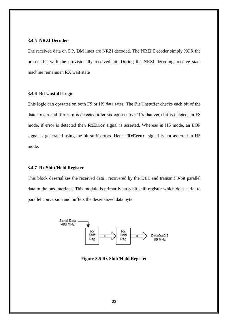
3.4.7 Rx Shift/Hold Register
This block deserializes the received data , recovered by the DLL and transmit 8-bit parallel
data to the bus interface. This module is primarily an 8-bit shift register which does serial to
parallel conversion and buffers the deserialized data byte.
Figure 3.5 Rx Shift/Hold Register

29
3.4.8 Receive State Machine
Figure 3.6 Receive state machine
Figure 3.7 Receive timing cycle

30
When the Reset signal is negated, the Receive State Machine enters the Wait state as shown.
There it starts looking for a SYNC pattern. When it has detected a SYNC pattern, the state
machine will enter the Strip SYNC state and assert RXActive. After receiving 8 bits of valid
serial data, the state machine enters the RX Data state where the data is loaded into the RX
Holding Register on the rising edge of CLK and RXValid is asserted. Stuffed bits are then
stripped from the data stream. Each time 8 stuffed bits are accumulated, state machine will
enter the RX Data Wait state, negating the RXValid.
When the EOP signal is detected, the state machine will enter the Strip EOP state and negate
RXActive and RXValid. After the EOP has been stripped the RX State Machine will re-enter
the Wait state and begin looking for the next packet.
If a Receive Error is detected in the process, the state machine enters Error State and RXError
is asserted. Then state machine enters either the Abort 1State where RXActive, RXValid, and
RXError signals are negated, or the Abort 2 State where only RXValid, and RXError signals
are negated
3.4.9 NRZI Encoder
The transmitted data on DP, DM lines are NRZI encoded. During the NRZI encoding,
transmit state machine remains in TX wait state. When bit ‘1’ is received in the serial data it
is negated and transmitted to DP, DM lines. Whereas when bit ‘0’ is encountered, it is
directly transmitted on to the DP, DM lines.
3.4.10 Bitstuff Logic
Bit stuffing is carried out so as to ensure adequate signal transition when sending data. A ‘0’
is inserted after every 6 consecutive 1s before the data is NRZI encoded. This is done to
enforce a transition in the NRZI data stream. SYNC pattern enables Bit stuffing.
After every 8 bits stuffed into the data stream, TxReady gets negated for one byte time so as
to hold up the data on to the DataIn bus.

31
3.4.11 Tx Shift/Hold Register
The module receieves 8bit parallel data and buffers in the Tx Hold Reg and then sends to 8-
bit shift register. This block primarily converts parallel data to serial data
Figure 3.8 Tx Shift/Hold Register
3.4.12 Transmit State Machine
Figure 3.9 Transmit state machine
Figure 3.10 Transmit timing cycle

32
When Reset signal is negated the, transmit state machine enters the TX Wait state.
In the TX Wait state, the TX state machine looks for the assertion of TXValid and when it is
detected, the state machine will enter the Send SYNC state and begin transmission of the
SYNC pattern. When the transmitter is ready for the first byte of the packet (PID), it enters
the TX Data Load state, TXReady is asserted and the TX Holding Register is loaded. The
state machine may enter the TX Data Wait state on completion of the SYNC pattern
transmission.
The state machine remains in the TX Data Wait state until the TX Data Holding register is
available for some more data. In the TX Data Load state, the state machine loads the
Transmit Holding register. The state machine will remain in TX Data Load state as long as
the transmit state machine can empty the TX Holding Register before the next rising edge of
CLK.
When TXValid is negated, the TX state machine enters the Send EOP state where it sends the
EOP. During the EOP transmission, TXReady signal is negated and the state machine will
remain in the Send EOP state. After the EOP is transmitted the Transmit State Machine
returns to the TX Wait state, looking for more data
3.4.13 USB HS/FS XCVR
Transmit driver: On enabling, the data from the transmiting data path will be driven into
DP/DM Signal lines. The HS/FS transmit driver becomes active only when it is asserted. The
XcvrSelect input is in HS/FS transceiver enabled mode.
Receive Buffer: On enabling, the received HS/FS data is multiplexed through the data path
of the receiver to the shift and hold register of the receiver. The USB receive buffers gets
active when the XcvrSelect input is in the HS transceiver enabled mode.

33
3.5 PROTOCOL LAYER
The protocol layer carries out all the USB data input/output and communications in the USB
core.
Figure 3.11 Protocol Layer overview
DMA and Memory Interface
DMA interfaces with the data memory. This provides DMA block transfer and random
memory access.
Protocol Engine
Protocol Engine performs USB’s standard handshake and control correspondence. These are
SOF tokens, ACK, NYET, NACK, replying to PING tokens.
34
Packet Assembly
This block collects the packets and puts then into the UTMI. First , it assembles the header,
then it inserts proper PID and Checksum , finally data field is added (if requested).
Packet Disassembly
This block recognizes the incoming packets and sends the decoded data to the proper block.
The decoding process includes extraction of PID and sequence number. Along with that
recognizing the header check sum is also carried out.
3.5.1 Buffer Operations
The buffer operations are carried out by buffer pointers which points to the I/O data
structures in the memory. If the value of buffer pointer is 7FFFh, then it indicates that the
buffer hasn’t been allocated yet. The core responds with a NAK to the USB host if all the
buffers are not allocated. Data transfer within buffer takes place in a Round Robin fashion.
Buffer 0 is used first when data is sent to/from an endpoint. The function controller is notified
through an interrupt when the Buffer 0 is empty/full. Buffer 0 can now be refilled/emptied by
the function controller. When the second buffer is empty/full, the function controller is
interrupted, and the USB core will use buffer 0 again, and so on.
A buffer can be larger than the MAXIMUM_PAYLOAD_SIZE. In that case, many packets
can retrieved/placed from/to a buffer. For an OUT endpoint, a buffer must always be
multiples of maximum payload size. The buffer size field should always be checked by the
software. When the entire buffer has been used, the buffer size is 0. If it is not 0, then the size
field indicates, the number of bytes of the buffer that has not been used.
There is no such limitation in case of IN buffers. The core will always transmit the maximum
possible number of bytes, which is the minimum of the payload size and remaining buffer
size.

35
Control endpoints can receive and transmit data. Hence in this case, Buffer0 is always an
OUT buffer and Buffer1 always an IN buffer.
Buffer underflow
A buffer underflow condition is specified, when either the expternal DMA engine or the
function controller has not filled the, the internal buffer with enough data for one
MAXIMUM_PAYLOAD_SIZE packet. In this condition, the USB core replies a NACK to
the host when an IN token is received.
Buffer overflow
A buffer overflow is specified when a packet, that has been received, doesn’t fit into the
buffer. The packet is discarded and a NACK is sent to the host. The USB core will continue
discarding the received data, and reply with NACK to each OUT token when payload size
doesn’t fit into the buffer.
3.5.2 DMA Operation
DMA operation allows a complete transparent movement of data from the USB core to the
functions attached. Each point is associated with a pair of dma_req and dma_ack signals.
The USB core will use these signals for DMA flow control when the dma_en bit is set in the
CSR register. When the buffer contains data or when the buffer is empty and needs to be
filled, the dma_req signal is asserted. The DMA responds with a dma_ack signal for each
word transferred.
Only Buffer 0 is used in DMA mode. The function controller is notified with an interrupt
when the received packet is less that the MAX_PL_SZ. In addition to it, the Buffer1 is set to
the local buffer address of that received packet. So as to carry out uninterrupted DMA
transfers, the buffer is padded by the USB core with the MAX_PL_SZ bytes.

36
3.5.3 Control Status Register (CSR)
The CSR acts as the control word of the DMA operation. The status and configuration bits
specify the type of operation mode.
BIT ACCESS DESCRIPTION
31:30 RO UC_BSEL (Buffer Select) This bits must be initialized to zero (first Buffer 0 is used) 00: Buffer 0 01: Buffer 1 1x: RESERVED
29:28 RO UC_DPD These two bits are used by the USB core to keep track of the data PIDs for high speed endpoints and for DATA0/DATA1 toggling.
27:26 RW EP_TYPE (Endpoint Type) 00: Control Endpoint 01: IN Endpoint 10: OUT Endpoint 11: RESERVED
25:24 RW TR_TYPE (Transfer Type) 00: Interrupt 01: Isochronous 10: Bulk 11: RESERVED
23:22 RW EP_DIS (Disable The Endpoint Temporarily) 00: Normal Operation 01: Force the core to ignore all transfers to this endpoint 10: Force the endpoint in to HALT state 11: RESERVED
21:18 RW EP_NO (Endpoint Number)
17 RW LRG_OK 1 - Accepts data packet of more than MAX_PL_SZ bytes (RX only) 0 - Ignores data packet with more than MAXPL_SZ bytes (RX only)
16 RW SML_OK 1 – Accepts data packet with less than MAX_PL_SZ bytes (RX only) 0 - Ignores data packet with less than MAXPL_SZ bytes (RX only)
15 RW DMAEN 1: Enables external DMA interface and operation 0: No DMA operation
12:11 RW TR_FR Number of transactions per micro frame (HS mode only)
10:0 RW MAX_PL_SZ Maximum payload size (MaxPacketSize) in bytes
Table 3.1 Control Status Register bit definition

37
3.6 PROTOCOL ENGINE
The protocol engine is responsible for CRC check and generation , packet identifier decoding
and verification, recognition of address and handshake evaluation and response. The protocol
engine acts on a received token and analyzes the token’s PID , address and endpoint number
fields. The protocol engine handles USB packets and transactions based on data sequencing
and state machine logic.
Protocol engine complies with High Speed USB 2.0 secification with a transfer rate of
480Mbit/s. It also meets UTMI specifications, generating control signals for UTMI
transceiver interface according to the FSM states.
There are 3 types of transactions: IN, OUT and SETUP.
There are 4 data transfer types: Control, Bulk, Interrupt and Isochronous.
3.6.1 Dataflow Types
CONTROL TRANSFER
Control transfers are used for initial configuration of the device by the host using
Endpoint 0 OUT and Endpoint 0 IN. The data delivery is lossless. It is divided into 3
stages SETUP, DATA and STATUS.
The SETUP stage carries an 8 bytes Setup packet which defines the request and
mentions the amount of data to be transferred in the DATA stage.
The DATA stage starts with a transaction which contains DATA1. The transaction
switches between DATA1 and DATA0 until all the required data is transferred.
The STATUS stage contains a zero-length DATA1 packet. For DATA stage as IN,
the STATUS stage is OUT and vice-versa.
Max packet size: 8 for low speed; 8, 16, 32 or 64 for full speed; 64 for high speed.
38
BULK TRANSFER
These are designed to transfer large amount of data with error free delivery without
any guarantee of bandwidth. Bulk data has a sequential form. If an IN/ OUT endpoint
is defined as using Bulk transfers, then the host will transfer data to it using IN/OUT
transactions respectively. Bulk transfer is not applicable for low speed.
Max packet size: 8, 16, 32 or 64 for full speed; 512 for high speed.
INTERRUPT TRANSFER.
Interrupt transfer are applicable to devices that need guaranteed quick responses (e.g.:
Pointing Devices and keyboards).These are regularly scheduled IN or OUT transfers.
Packet size may vary from 1-8 bytes at low speed and 1-64 for full speed or upto 1024
bytes at high speed
ISOCHRONOUS TRANSFER
Isochronous transfers give a guaranteed bandwidth but without any guarantee of
error-free delivery. A special feature of this transfer is, there is no handshake packet at
the end. Applications such as audio data transfer follow isochronous mode of data
transfer because it is important to maintain a constant flow of data.
It uses either OUT or IN transaction depending on the type of endpoint.
It is not applicable for low speed data transfer. Packet size varies upto 1023 bytes at
full speed or upto 1024 at high speed.

39
Chapter 4
SIMULATIONS
& RESULTS

40
4.1 UTMI SIGNALS SIMULATION
In the simulation, the rx_data contained Up-Counter values and tx_data contained Down-
Counter values. For successful initiation of data transfer, the control signal tx_valid and
rx_valid must be asserted. Whenever tx_first is negated, the data_out remains the previous
value until the tx_first is asserted again.
In the simulation, the value 8’hFE gets stored because tx_first become low at 1.2us. It
regains data at the time 3us when tx_ready becomes high.
Figure 4.1 UTMI waveform

41
4.2 PACKET ASSEMBLY SIMULATION
The the waveform gives the packet simulation resuts. The input data was given using tx_data
signal as Up-Counter. This signal comes from the buffer memory and then to be transmitted
to UTMI. In the diagram, The CRC value of 8’h7C gets attached to data. This CRC value is
the lower byte of the signal crc16_rev. The lower byte got selected because crc_sel2 is high.
After CRC, token PID gets attached responding to the control signal send_token. When that
signal got asserted, token pid 8’h1E got attached. And so on.
The CRC, data PIDs, token PIDs get attached depending on the status the control signals.
Figure 4.2 Packet Assembly waveform

42
4.3 PACKET DISASSEMBLY SIMULATION
Unlike Packet Assembly, in packet Disassembly, the reverse phenomenon occurs. The Data
coming from the UTMI through the signal rx_data, is decoded to get the Packet IDs and
Data IDs and then stored the buffer memory. In the waveform, the rx_data signal is
considered as an Up-Counter hence it is not justified to expect for the PIDs to be in proper
order. In the result we got the data PIDs and token PIDs matching with its corresponding PID
values.
Figure 4.3 Packet Disassembly waveform
43
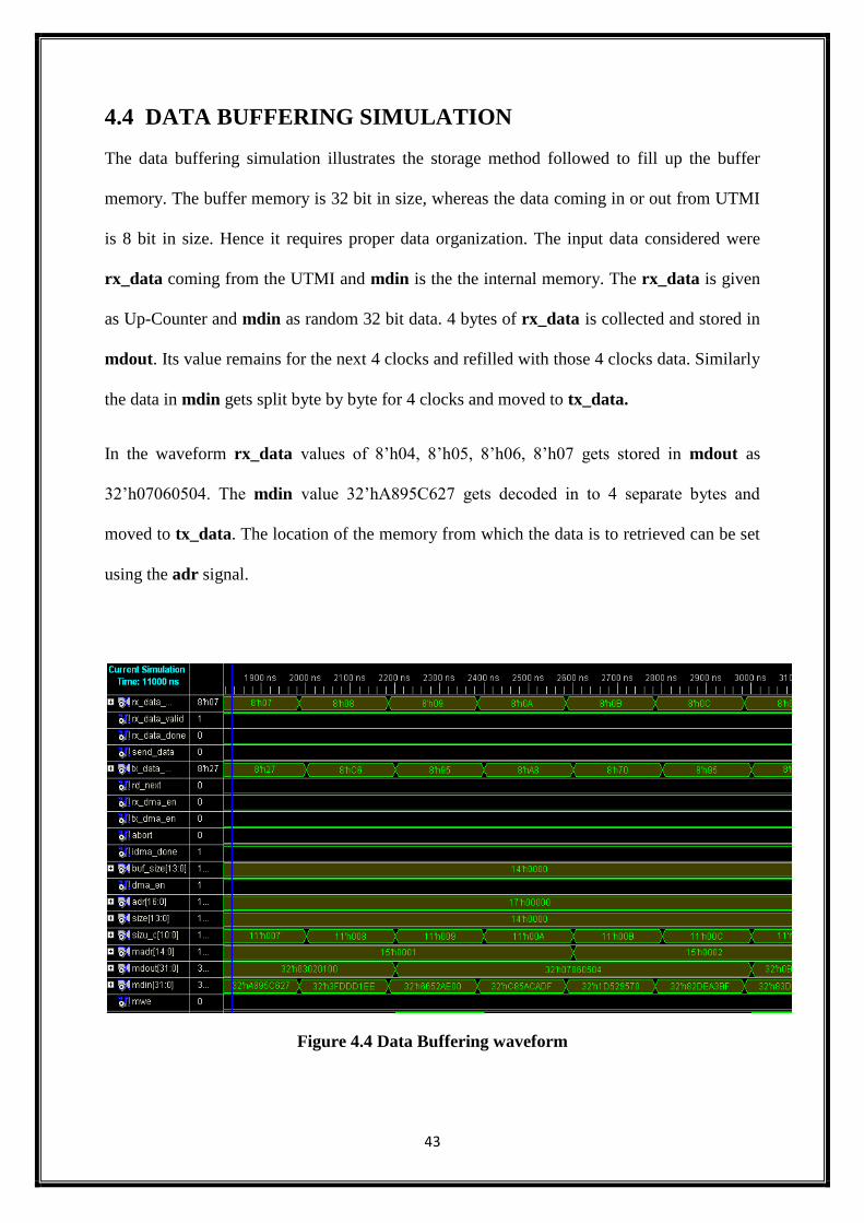
4.4 DATA BUFFERING SIMULATION
The data buffering simulation illustrates the storage method followed to fill up the buffer
memory. The buffer memory is 32 bit in size, whereas the data coming in or out from UTMI
is 8 bit in size. Hence it requires proper data organization. The input data considered were
rx_data coming from the UTMI and mdin is the the internal memory. The rx_data is given
as Up-Counter and mdin as random 32 bit data. 4 bytes of rx_data is collected and stored in
mdout. Its value remains for the next 4 clocks and refilled with those 4 clocks data. Similarly
the data in mdin gets split byte by byte for 4 clocks and moved to tx_data.
In the waveform rx_data values of 8’h04, 8’h05, 8’h06, 8’h07 gets stored in mdout as
32’h07060504. The mdin value 32’hA895C627 gets decoded in to 4 separate bytes and
moved to tx_data. The location of the memory from which the data is to retrieved can be set
using the adr signal.
Figure 4.4 Data Buffering waveform

44
4.4 PROTOCOL ENGINE SIMULATION
For the simulation of Protocol Engine we have considered IN and OUT transaction in
isochronous mode. These states were set using the CSR (Control Status Register) bits.
The following diagram shows the main flow chart.
Figure 4.5 USB core main flow chart
Figure 4.6 IN Cycle Figure 4.7 OUT cycle

45
In the protocol engine waveform initially an IN transaction was carried out. By this the
tx_dma_en signal will get set. The buffer 1 gets activated and the address of buffer 1 ( h’88)
gets stored in adr. The size of buffer 1 gets stored in the signal buf_size. After getting into
IN cycle, the data is sent. This is indicated by the pid_data0 and hence change in data_pid
signal was observed. After completion of 1 transaction we consider OUT transaction. The
rx_dmaen signal get set. The buffet 0 gets activated and the address of buffer 0 (h’80) gets
stored in adr. The size of buffer 0 gets stored in the adr and the process goes on. It was taken
care that the MAX_PL_SZ (indicated by bit 10:0 of CSR) is less than the size of buffers. If
the size becomes more than CSR then the transaction gets aborted. The signal idin and state,
next_state signals updates the PID and transaction states
Figure 4.8 Protocol Engine waveform

46
Chapter 5
CONCLUSION

47
5.1 CONCLUSION
Universal Serial Bus (USB) was developed as a means to connect a large number of
peripheral devices to the PC. USB 2.0 is an industry-wide, host oriented protocol, utilizing
physical serial bus. It is host controlled i.e. there can be only 1 host per bus. The
Communication flow complies with USB 2.0 Specifications essential for basic data transfer.
The USB host is responsible for undertaking all transactions and scheduling the bandwidth.
Data can be sent by various transaction methods using a token-based protocol. The USB
Specification defines three data speeds: Low speed (1.5Mbit/s), Full speed (12 Mbit/s) and
High speed (480Mbit/s).
With the introduction of USB 2.0 a new Host Controller Interface Specification, the EHCI
(Enhanced Host Controller Interface) came into existence to keep device development costs
down. It handles high speed transfers, and hand over low and full speed transfers to either
OHCI or UHCI companion controllers. EHCI uses a NRZI (Non Return to Zero Invert)
encoding scheme to send data with sync field to synchronize the host and receiver clocks.
We simulated a UTMI and protocol layer modules of the USB core in XILINX ISE 10.1. The
results were verified with test bench generation. It is observed that UTMI is a serial bus
interface which deals with USB protocols and signalling. The protocol engine also meets
UTMI specification, generating control signals for UTMI transceiver interface according to
the FSM states.

48
Chapter 6
FUTURE WORK

49
6.1 FUTURE WORK
To develop the whole USB core, other verilog modules for memory arbriter, register file,
function interface needs to be designed, synthesized and simulated.
Since the USB 2.0 is widely used in many peripheral devices. It is well established and has
already proved itself to be reliable and efficient. The protocol's strict restrictions assure that
different devices are compatible in every machine. This assures that the Protocol Engine we
designed can be used in various products that uses USB2.0 standard as their chosen protocol.
An advance version of the Protocol Engine would be an assimilation of the DMA Controller
into it. Including the DMA Controller would simplify the interface with the device’s bus and
reduce chances of bus contention by upgrading the synchronization capabilities of the
Protocol Engine in the USB device.
Furthermore, USB3.0 spec has been published and not long from now the computer industry
will adopt this standard and move forward to the more advance protocol. A future
improvement for the Protocol Engine is to support USB3.0 features and speed.

50
REFERENCES
[1] Axelson, Jan, (2001), USB Complete: Everything You Need to Develop Custom USB
Peripherals. Third Edition
[2] Fatemeh Arbab Jolfaei et al., High Speed USB 2.0 Interface for FPGA Based
Embedded Systems, Isfahan University of Technology, Department of Electrical
& Computer Engineering
[3] Universal Serial Bus Specifications Revision 2.0
[4] www.usb.org [online]
[5] ” USB Made Simple”,Available at : http://www.usbmadesimple.co.uk/index.html
[6] "USB in a nutshell, making sense of the USB standard", Craig Peacock, Nov 2002,
Available at: www.beyondlogic.org
[7] USB 2.0 Transceiver Macrocell Interface (UTMI): Retrieved from
http://www.intel.com/technology/usb/download/2_0_xcvr_macrocell_1_05.pdf
[8] Jan Axelson, USB Complete - Everything you need to develop custom USB
peripherals, Lakeview research, 3rd Edition, Aug 2005
[9] "libUSB Manual", libUSB Project, Available at: http://libusb.sourceforge.net/
[10] "Spartan-3 FPGA Family: Complete Data Sheet", Xilinx Corp., Aug 2005