FPGA BASED HIGH SPEED DATA ACQUISITION SYSTEM WITH ... · FPGA BASED HIGH SPEED DATA ACQUISITION...
4
International Journal of Advances in Science Engineering and Technology, ISSN: 2321-9009 Volume- 2, Issue-3, July-2014 FPGA Based High Speed Data Acquisition System With Ethernet Interface 99 FPGA BASED HIGH SPEED DATA ACQUISITION SYSTEM WITH ETHERNET INTERFACE SUMA G S M.Tech Student, Shri Ramdeobaba College of Engineering and Management, Nagpur Email: [email protected] Abstract --To develop FPGA based 16 channel high speed Data Acquisition System with Ethernet interface is the objective of this paper. PQFP208 APA300 FPGA of ProASIC family belongs to Altera is used for this Data Acquisition System. The input data is acquired through 16 channels Analog Multiplexer is given to Analog to Digital converter. The digital data is stored in the buffer. The further processing is done by the 16 bit processor implemented in the FPGA by using VHDL. The IDE tool libero 9.1v is used for the implementation of the processor. The input control unit and the 16 bit processor is used to set up and initialize the input data source, Ethernet controller and data flow from the memory to the Network Interface. With FPGA as the platform we are getting the advantages of flexibility, programmability, low power consumption etc. The electrical isolation is one of the important requirements DAQ System, which is the main advantage that can be obtained with Ethernet interface. If multiple DAQ units are using, then synchronization is also an important need. To get the same the Precision Clock Synchronization Protocol (PTP/IEEE 1588) is used. Keywords:- Field Programmable Gate Array(FPGA), Ethernet, Data Acquisition System (DAQ System), Precision Time Protocol (PTP). I. INTRODUCTION Data Acquisition System is the process of collection, for the purpose of analyzing the data for various applications such as communication, telemetry, remote sensing, space application etc. During the early stage the main controlling unit used in DAQ Systems is microcontroller. In these systems all the data processing is done using the microcontroller unit. Even though this system has the advantages of low cost, low power consumption and smaller size, it has got several drawbacks such as low processing speed and poor usage of memory resources. Nowadays speed and size is the main constraints. So embedded field now uses Advanced RISC Machines (ARM), DSP chips and FPGA as the main controlling unit in the data acquisition system. Three of them are having advantages of their own in their application. So they are selected as per the application. ARM has a formidable transaction management function. It is mainly used in embedded control, multimedia, mobile applications and other areas. The main advantages of DSP are its strong data processing capability and high operating speed. DSP are mainly used to greatly reduce the control system computation and band width requirement. Because of the advantages of flexibility, parallelism and reconstruction which are much better than the other chips, FPGA is developing rapidly. So find more application of FPGA to implement the glue logic, signal processing and for developing system using System on Chip [4]. Due to parallel processing capability, FPGA can be used for the implementation of the highly complex structure. Now consider the medium used for the transmission of data. We are using different types of DAQ Systems such as serial communication data acquisition system, Universal Serial Bus (USB) data acquisition system etc. RS232, RS422 and RS485 are used for serial communication system. Transmission distances, data rate it can support are the main limitation. The maximum cable length that can support by RS232 is up to 50 ft and cannot increase the frequency above some certain range. RS485 is RS422 can support more transmission range and high frequency. But the electrical isolation is the main requirement of DAQ which can be obtained with Ethernet communication. By using parallel port computers can connected to the DAQ, has the advantage of higher sampling rate. There also can distance is limited to few feet.USB is the new technology used in the field DAQ, which can support higher bandwidth [1]. Now the USB 3.1 standard introduced with the signaling rate to 10 Gbit/s, double that of USB 3.0, and reduces line encoding overhead to just 3% by changing the encoding scheme to 128b/132b. The FPGA based Ethernet DAQ system has the advantage of flexibility in the sense that change of Ethernet protocol only requires uploading of FPGA configuration and software for the selected protocol. So without much effort the future protocol can be supported at any time. Since general FPGA programming languages such as VHDL is used, it is so easy to switch to another vendor. So it is not vendor specific. Some of the application requires the acquisition of data from different DAQ module. To reduce complexity, weight and interconnection unit Ethernet is used for interconnect. Then data samples acquired should be on the same time. For that synchronization of the entire module is required. This is the concept of development of distributed DAQ system. Adapt IEEE1588 standard(“Precision clock synchronization
Transcript of FPGA BASED HIGH SPEED DATA ACQUISITION SYSTEM WITH ... · FPGA BASED HIGH SPEED DATA ACQUISITION...
International Journal of Advances in Science Engineering and Technology, ISSN: 2321-9009 Volume- 2, Issue-3, July-2014
FPGA Based High Speed Data Acquisition System With Ethernet Interface
99
FPGA BASED HIGH SPEED DATA ACQUISITION SYSTEM WITH ETHERNET INTERFACE
SUMA G S
M.Tech Student, Shri Ramdeobaba College of Engineering and Management, Nagpur
Email: [email protected]
Abstract --To develop FPGA based 16 channel high speed Data Acquisition System with Ethernet interface is the objective of this paper. PQFP208 APA300 FPGA of ProASIC family belongs to Altera is used for this Data Acquisition System. The input data is acquired through 16 channels Analog Multiplexer is given to Analog to Digital converter. The digital data is stored in the buffer. The further processing is done by the 16 bit processor implemented in the FPGA by using VHDL. The IDE tool libero 9.1v is used for the implementation of the processor. The input control unit and the 16 bit processor is used to set up and initialize the input data source, Ethernet controller and data flow from the memory to the Network Interface. With FPGA as the platform we are getting the advantages of flexibility, programmability, low power consumption etc. The electrical isolation is one of the important requirements DAQ System, which is the main advantage that can be obtained with Ethernet interface. If multiple DAQ units are using, then synchronization is also an important need. To get the same the Precision Clock Synchronization Protocol (PTP/IEEE 1588) is used. Keywords:- Field Programmable Gate Array(FPGA), Ethernet, Data Acquisition System (DAQ System), Precision Time Protocol (PTP). I. INTRODUCTION Data Acquisition System is the process of collection, for the purpose of analyzing the data for various applications such as communication, telemetry, remote sensing, space application etc. During the early stage the main controlling unit used in DAQ Systems is microcontroller. In these systems all the data processing is done using the microcontroller unit. Even though this system has the advantages of low cost, low power consumption and smaller size, it has got several drawbacks such as low processing speed and poor usage of memory resources. Nowadays speed and size is the main constraints. So embedded field now uses Advanced RISC Machines (ARM), DSP chips and FPGA as the main controlling unit in the data acquisition system. Three of them are having advantages of their own in their application. So they are selected as per the application. ARM has a formidable transaction management function. It is mainly used in embedded control, multimedia, mobile applications and other areas. The main advantages of DSP are its strong data processing capability and high operating speed. DSP are mainly used to greatly reduce the control system computation and band width requirement. Because of the advantages of flexibility, parallelism and reconstruction which are much better than the other chips, FPGA is developing rapidly. So find more application of FPGA to implement the glue logic, signal processing and for developing system using System on Chip [4]. Due to parallel processing capability, FPGA can be used for the implementation of the highly complex structure. Now consider the medium used for the transmission of data. We are using different types of DAQ Systems such as serial communication data acquisition system,
Universal Serial Bus (USB) data acquisition system etc. RS232, RS422 and RS485 are used for serial communication system. Transmission distances, data rate it can support are the main limitation. The maximum cable length that can support by RS232 is up to 50 ft and cannot increase the frequency above some certain range. RS485 is RS422 can support more transmission range and high frequency. But the electrical isolation is the main requirement of DAQ which can be obtained with Ethernet communication. By using parallel port computers can connected to the DAQ, has the advantage of higher sampling rate. There also can distance is limited to few feet.USB is the new technology used in the field DAQ, which can support higher bandwidth [1]. Now the USB 3.1 standard introduced with the signaling rate to 10 Gbit/s, double that of USB 3.0, and reduces line encoding overhead to just 3% by changing the encoding scheme to 128b/132b. The FPGA based Ethernet DAQ system has the advantage of flexibility in the sense that change of Ethernet protocol only requires uploading of FPGA configuration and software for the selected protocol. So without much effort the future protocol can be supported at any time. Since general FPGA programming languages such as VHDL is used, it is so easy to switch to another vendor. So it is not vendor specific. Some of the application requires the acquisition of data from different DAQ module. To reduce complexity, weight and interconnection unit Ethernet is used for interconnect. Then data samples acquired should be on the same time. For that synchronization of the entire module is required. This is the concept of development of distributed DAQ system. Adapt IEEE1588 standard(“Precision clock synchronization
International Journal of Advances in Science Engineering and Technology, ISSN: 2321-9009 Volume- 2, Issue-3, July-2014
FPGA Based High Speed Data Acquisition System With Ethernet Interface
100
protocol for networked measurement and control systems”) to implement the DAQ system for the distribution of the time with accuracy of 1µS , having the Ethernet interface for transmission of data. The PTP (Precision Time Protocol) management block is implemented in hardware using FPGAs and message time-stamping is applied at the PHY layer. These result in minimal protocol stack jitter and improved accuracy. II. PROPOSED DESIGN OF THE OVERALL
SYSTEM Block Diagram
Fig[i]. Block diagram of Proposed Design
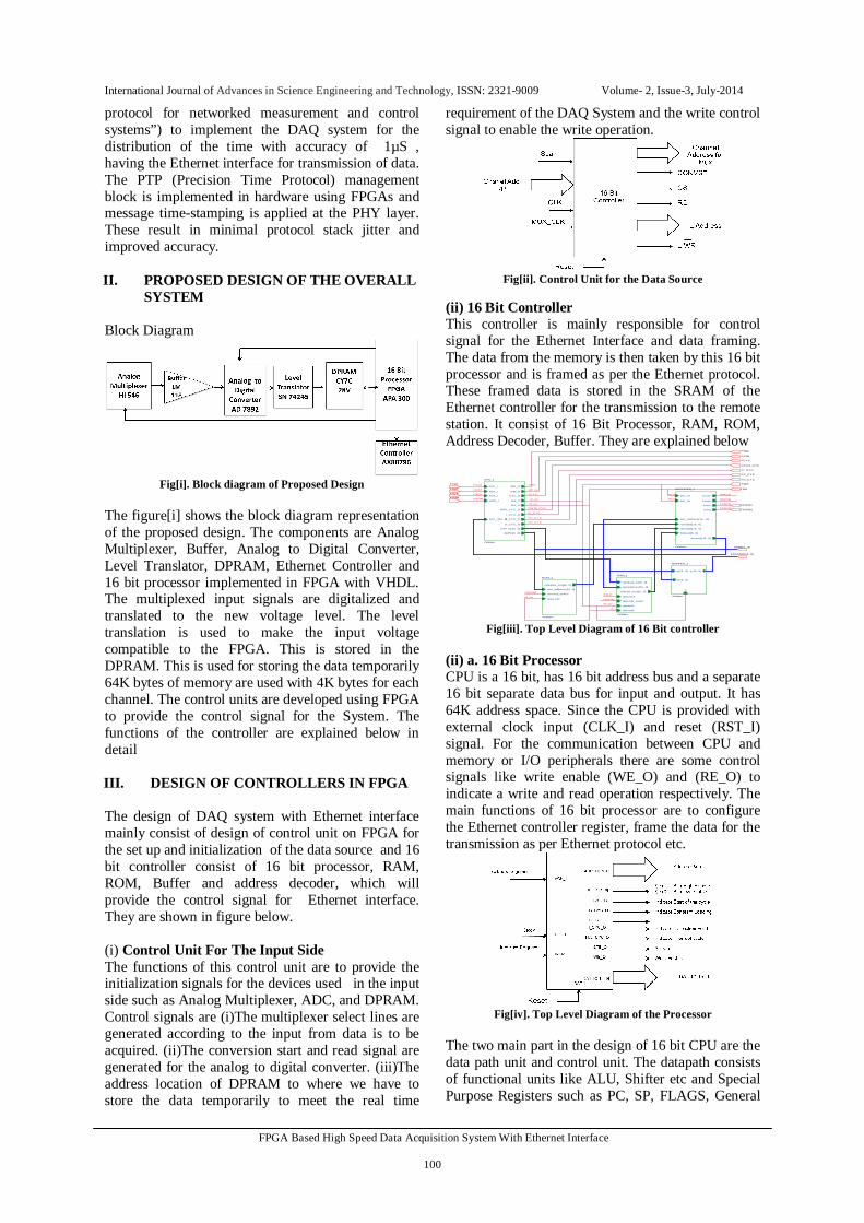
The figure[i] shows the block diagram representation of the proposed design. The components are Analog Multiplexer, Buffer, Analog to Digital Converter, Level Translator, DPRAM, Ethernet Controller and 16 bit processor implemented in FPGA with VHDL. The multiplexed input signals are digitalized and translated to the new voltage level. The level translation is used to make the input voltage compatible to the FPGA. This is stored in the DPRAM. This is used for storing the data temporarily 64K bytes of memory are used with 4K bytes for each channel. The control units are developed using FPGA to provide the control signal for the System. The functions of the controller are explained below in detail III. DESIGN OF CONTROLLERS IN FPGA The design of DAQ system with Ethernet interface mainly consist of design of control unit on FPGA for the set up and initialization of the data source and 16 bit controller consist of 16 bit processor, RAM, ROM, Buffer and address decoder, which will provide the control signal for Ethernet interface. They are shown in figure below. (i) Control Unit For The Input Side The functions of this control unit are to provide the initialization signals for the devices used in the input side such as Analog Multiplexer, ADC, and DPRAM. Control signals are (i)The multiplexer select lines are generated according to the input from data is to be acquired. (ii)The conversion start and read signal are generated for the analog to digital converter. (iii)The address location of DPRAM to where we have to store the data temporarily to meet the real time
requirement of the DAQ System and the write control signal to enable the write operation.
Fig[ii]. Control Unit for the Data Source
(ii) 16 Bit Controller This controller is mainly responsible for control signal for the Ethernet Interface and data framing. The data from the memory is then taken by this 16 bit processor and is framed as per the Ethernet protocol. These framed data is stored in the SRAM of the Ethernet controller for the transmission to the remote station. It consist of 16 Bit Processor, RAM, ROM, Address Decoder, Buffer. They are explained below
Fig[iii]. Top Level Diagram of 16 Bit controller
(ii) a. 16 Bit Processor CPU is a 16 bit, has 16 bit address bus and a separate 16 bit separate data bus for input and output. It has 64K address space. Since the CPU is provided with external clock input (CLK_I) and reset (RST_I) signal. For the communication between CPU and memory or I/O peripherals there are some control signals like write enable (WE_O) and (RE_O) to indicate a write and read operation respectively. The main functions of 16 bit processor are to configure the Ethernet controller register, frame the data for the transmission as per Ethernet protocol etc.
Fig[iv]. Top Level Diagram of the Processor
The two main part in the design of 16 bit CPU are the data path unit and control unit. The datapath consists of functional units like ALU, Shifter etc and Special Purpose Registers such as PC, SP, FLAGS, General
FRST
FDATAIO[15..0]
RAM_1
<Value>
ramdata_in[15..0]
ramaddress[10..0]
ramclock
ramchip_select
ramwrite
ramread
ramdat_out[15..0]romchip
BUFFER_1
<Value>
y [15..0]
b[15..0]
a[15..0]
e
rd_oo
FI_CYC
DECODER_1
<Value>
dec_rd
dec_wr
csrom
csram
csio1
csio2
muxout[15..0]
dec_address[15..11]
romdata[15..0]
ramdata[15..0]
bidata[15..0]
FRST
FSTB
wr_oo
FRD
rd_oo
FSEL
FCLK
ROM_1
<Value>
rom_address[10..0]
romchip_select
read_rom
romdata_out[15..0]
romchip
FCSIO2
FC_CYC
wr_oo
FCSIO1
FACK
FI_CYC
FINTR
ADR[15..0]
FCYC
ramchip
FCSIO2
ramchip
FCLK
rd_oo
FWR
FC_CYC
rd_oo
FACK
CPU_1
<Value>
SEL_O
STB_O
CYC_O
WE_O
RD_O
INTA_CYC_O
I_CYC_O
C_CYC_O
D_CYC_O
DAT_O[15..0]
ADR[15..0]
CLK_I
RST_I
ACK_I
INTR_I
DAT_I[15..0]
FSEL
stb_oo
FINTR
FCLK
FCYC
wr_oo
FINTA_CYC
FCSIO1
FD_CYC
FINTA_CYC
FD_CYC

International Journal of Advances in Science Engineering and Technology, ISSN: 2321-9009 Volume- 2, Issue-3, July-2014
FPGA Based High Speed Data Acquisition System With Ethernet Interface
101
purpose registers, along with several other units and multiplexers. The datapath inputs are control signals like load control signals of registers, data select signals of multiplexers, operation select signals of ALU and Shifter and Clock input. The data bus is used for both input and output operations. The control unit of the processor is implemented as melay machine. All the state transitions are on the rising edge of the clock. The entire control signal required for the Datapath section are generates by the control unit.
Fig[v] Data Path Diagram
(ii) b. Random Access Memory (Ram) Memory is required for the storing of the program as well as data.Here the memory is mainly configured as storing the data.Here the RAM is implemented as 2048 X 16 supporting synchronous read and write operations in VHDL with 11 address lines(10..0). For its implementation we used generic VHDL, instead of instantiating RAM primitives provided in vendor library. There is separate process for read and write operation. With the rising edge of the clock, assertion of chip enable signal and operation enable (read, write) the desired operation is performed. (ii) c. Read Only Memory (Rom) ROM is implemented as 2048 X 16 supporting read operations in VHDL with 11 address lines(10..0). For its implementation we used generic VHDL. With the assertion of chip enable signal and read, the selected memory is read and the data will be available on the romdataout output. (ii) d. Address Decoder The decoder module having the input read ,write(rd_oo,wr_oo) and adress lines(ADR(15..11)) signal which are generated from CPU. The Data
linesfrom the ROM, RAM and input through buffer are also connected as input of the decoder. The enable signals for RAM and ROM is from the decoder as 'romchip' and 'ramchip'. The output from the buffer, RAM and ROM are connected to the input of decoder and the output from the decoder is connected to the input DATA bus of CPU as DAT_I. The four chip select signals (ramchip, romchip, FCSO1,FCSIO2) are generated by address decoder according to the input address lines, RD_O and WE_O. The FCSIO1 and FCSIO2 is the chip select for the DPRAM and Ethernet controller respectively. The address lines A [15..11] are connected to the address decoder to get this chip select line. (ii) e. Bidirectional Buffer The buffer multiplexes the internal input and output data line, to form multiplexed IO lines externally and also it de-multiplexes the external IO lines to form separate input and output data lines to use internally. It is enabling with the write enable signal from the CPU. IV. SIMULATION RESULT All the simulations of VHDL are done by using Libero IDE 9.1software. The simulated results of control and initialization signals for the input devices such as Analog Mux, ADC, DPRAM and transmission of data to the Ethernet controller are shown in fig[vi], fig[vii] respectively. For the input side the mux select signals or channel address are generated either sequentially for acquiring the input signals from the all of the channel or a particular channel address to acquire the input from the specific channel. The conversion start signals read signals are generated for the ADC to get the corresponding digital data. The memory address and the write signals are generated corresponding to the channel from which we are acquiring the data. The data from DPRAM is taken by the FPGA processor and is transferred to the Ethernet controller by using move string instruction. The simulated waveforms of the processor, used for this data transmission are shown in figure. The active high reset signal is high during the first 5 clock cycle to rest all the operation of the processor. All of the input signals are given through the test bench. All of the operations are synchronized with positive edge of the clock. When read or write operations are completed the acknowledge signal (ack_i) becomes high. The intr_i is an active high input signal to indicate the status of interrupt from any other peripheral. To indicate the location of data on the bus during read and write operation the outputs sel_o is there. If there is a valid data transfer occurs then the strobe output is high. To indicate instruction fetch, data load and constant fetch, the signals used are i_cyc_o, d_cyc_o, c_cyc_o respectively. we_o, rd_o are the control signal for the read and write

International Journal of Advances in Science Engineering and Technology, ISSN: 2321-9009 Volume- 2, Issue-3, July-2014
FPGA Based High Speed Data Acquisition System With Ethernet Interface
102
operation. The address bus and data bus are indicated with adr_o, dat_io. The output data is available on the dat_io output if there is a valid write cycle occurs. If A [15..11] is 00011 then FCSIO2 is active. So the address above “0X1800” Ethernet will be selected.
Fig[vi] Simulated waveform for the input side devices (for
Analog Mux, ADC, DPRAM)
Fig[vii] Simulated waveform for Initialization of Ethernet
Controller
Fig[viii] Simulated waveform for Data Transfer from FPGA to
data port of Ethernet Controller
CONCLUSIONS In this paper the implementation of FPGA based data acquisition with Ethernet is explained. Since the entire control and initialization signal of the total systems is generated with FPGA, the advantages of low power, design flexibility, high efficiency and fewer on board components are obtained. Here Ethernet is used as the medium for the data transfer. Due to this the system is faster and vendor independent. The data can be acquired from the multiple devices the advantage of distributed network is also obtained. REFERENCES
[1] Bi Bo, Sun Shuying, Wang Chunping, “Design of Data Acquisition Equipment Based on USB”, The Eighth International Conference on Electronic Measurement and Instruments,2007,pp.866-899.
[2] Hong Yongqiang ,Yang Jinhong, ‚Design of UART Based
on ARM+DSP Distributed Data Acquisition System‛, The Eighth International Conference on Electronic Measurement and Instruments,2007,pp.813-815.
[3] Biju Varghese, Changsheng Guo, Robert Gao, Stephen
Malkin, Sumukh Pathare, ‚A DSP-Based Telemetric Data Acquisition System for In-Process Monitoring of Grinding Operation”, IEEE Instrumentation and Measurement Technology Conference,1998,pp.191-196
[4] Wang Fei, Wu Zhijie, Chen Hong, Xi Yi2, " High-Speed
Data Acquisition System Based on FPGA/SoPC,” The Tenth International Conference on Electronic Measurement & Instruments, 2011, pp.21-27 [8].
[5] Swamy TN, Rashmi KM, “Data Acquisition System based
on FPGA ” , International Journal of Engineering Research and Applications (IJERA) ISSN: 2248-9622 www.ijera.com Vol. 3, Issue 2, March -April 2013, pp.1504-1509