(four spaces from top margin) - UTAR Institutional...
158
COMPACT REAL-TIME CONTROL SYSTEM OF AUTONOMOUS VEHICLE SYSTEM USING FPGA PLATFORM By CHAN KIM CHON A thesis submitted to the Department of Mechatronics and BioMedical Engineering, Faculty of Engineering and Science, Universiti Tunku Abdul Rahman, in partial fulfillment of the requirements for the degree of Master of Engineering Science December 2011
Transcript of (four spaces from top margin) - UTAR Institutional...
COMPACT REAL-TIME CONTROL SYSTEM OF AUTONOMOUS
VEHICLE SYSTEM USING FPGA PLATFORM
By
CHAN KIM CHON
A thesis submitted to the Department of Mechatronics and BioMedical
Engineering,
Faculty of Engineering and Science,
Universiti Tunku Abdul Rahman,
in partial fulfillment of the requirements for the degree of
Master of Engineering Science
December 2011
ii
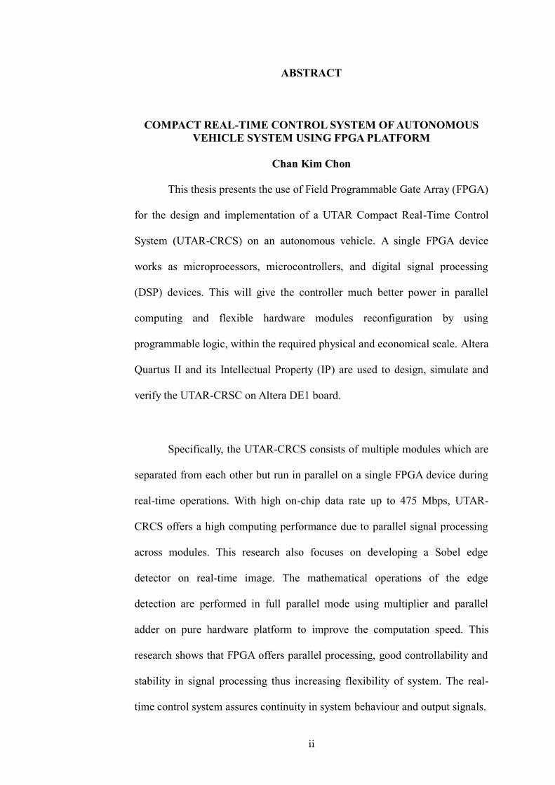
ABSTRACT
COMPACT REAL-TIME CONTROL SYSTEM OF AUTONOMOUS
VEHICLE SYSTEM USING FPGA PLATFORM
Chan Kim Chon
This thesis presents the use of Field Programmable Gate Array (FPGA)
for the design and implementation of a UTAR Compact Real-Time Control
System (UTAR-CRCS) on an autonomous vehicle. A single FPGA device
works as microprocessors, microcontrollers, and digital signal processing
(DSP) devices. This will give the controller much better power in parallel
computing and flexible hardware modules reconfiguration by using
programmable logic, within the required physical and economical scale. Altera
Quartus II and its Intellectual Property (IP) are used to design, simulate and
verify the UTAR-CRSC on Altera DE1 board.
Specifically, the UTAR-CRCS consists of multiple modules which are
separated from each other but run in parallel on a single FPGA device during
real-time operations. With high on-chip data rate up to 475 Mbps, UTAR-
CRCS offers a high computing performance due to parallel signal processing
across modules. This research also focuses on developing a Sobel edge
detector on real-time image. The mathematical operations of the edge
detection are performed in full parallel mode using multiplier and parallel
adder on pure hardware platform to improve the computation speed. This
research shows that FPGA offers parallel processing, good controllability and
stability in signal processing thus increasing flexibility of system. The real-
time control system assures continuity in system behaviour and output signals.

iii
ACKNOWLEDGEMENTS
It would not have been possible to write this thesis without the help
and support of the kind people around me.
In the first place I would like to thank my supervisor, Associate
Professor Dr Tan Ching Seong for his supervision, advice, and guidance from
the very early stage of this research as well as giving me extraordinary
experiences throughout the work. Above all and the most needed, he provided
me unflinching encouragement and support in various ways.
I am most grateful to my fellow research mates, Tee Yu Hon and Teoh
Chee Way for their assistance in various occasions. I also wish to thank
workplace mates for the great environment and joyful atmosphere while
carrying out this research. I would like to acknowledge the financial, academic
and technical support of the Tunku Abdul Rahman University.
Finally, I would like express my heartfelt gratitude to dear family for
their continuous encouragement, understanding and love. I would like to
dedicate this work to them.

iv
APPROVAL SHEET
This thesis entitled “COMPACT REAL-TIME CONTROL SYSTEM OF
AUTONOMOUS VEHICLE SYSTEM USING FPGA PLATFORM” was
prepared by CHAN KIM CHON and submitted as partial fulfillment of the
requirements for the degree of Master of Engineering Science at Universiti
Tunku Abdul Rahman.
Approved by:
___________________________
(Dr Wang Chan Chin)
Date: 29 December 2011
Dean
Associate Professor
Department of Mechanical and Material Engineering
Faculty of Engineering and Science
Universiti Tunku Abdul Rahman

v
FACULTY OF ENGINEERING AND SCIENCE
UNIVERSITI TUNKU ABDUL RAHMAN
Date: 29 December 2011
SUBMISSION OF THESIS
It is hereby certified that CHAN KIM CHON (ID No: 09UEM09145 ) has
completed this thesis entitled “COMPACT REAL-TIME CONTROL SYSTEM
OF AUTONOMOUS VEHICLE SYSTEM USING FPGA PLATFORM” under
the supervision of Dr Tan Ching Seong (Supervisor) from the Department of
Mechatronics and BioMedical Engineering, Faculty of Engineering and Science.
I understand that University will upload softcopy of my thesis in pdf format into
UTAR Institutional Repository, which may be made accessible to UTAR
community and public.
Yours truly,
___________________
(CHAN KIM CHON)
____________________
(Student Name)

vi
DECLARATION
I hereby declare that the dissertation is based on my original work except for
quotations and citations which have been duly acknowledged. I also declare
that it has not been previously or concurrently submitted for any other degree
at UTAR or other institutions.
Name: CHAN KIM CHON
Date: 29 December 2011
vii
TABLE OF CONTENTS
Page
ABSTRACT II
ACKNOWLEDGEMENTS III
APPROVAL SHEET IV
DECLARATION VI
TABLE OF CONTENTS VII
LIST OF TABLES IX
LIST OF FIGURES X
LIST OF ABBREVIATIONS XII
CHAPTER
1.0 INTRODUCTION 1 1.1 Research Motivation 1
1.2 Scope of Research 7
1.3 Thesis Outline 8
2.0 LITERATURE REVIEW 10 2.1 Overview 10
2.2 Review of Control System for Autonomous Vehicle 11
2.2.1 Control System on LAGR 11
2.2.2 Control System on SAUVIM 14
2.2.3 Control System on ATRV 17
2.2.4 Control System on DEMO III 18
2.3 Challenges in Compact Real-Time Control System 20
2.4 Summary 23
3.0 UTAR COMPACT REAL-TIME CONTROL SYSTEM 28 3.1 Overview 28
3.2 UTAR-CRCS 29
3.2.1 Hardware Description 31
3.3 Design Methodology 40 3.3.1 VHDL and Verilog Constructs for FPGA Logic
Design 43
3.4 UTAR-CRCS Implementation 44
3.4.1 FPGA-based System Architecture 45
3.4.2 Module Specifications 46
3.4.3 Communication 52
3.4.4 UTAR-CRCS Clock Management 57
3.5 Summary 59

viii
4.0 FPGA BASED MACHINE VISION 60 4.1 Overview 60
4.2 Terasic TRDB_D5M Colour Camera 62
4.3 Block Diagram of Digital Camera Design 63
4.4 Block Diagram of Digital Camera Design with Sobel Edge
Detection 65
4.5 Sobel Edge Detector 66
4.6 FPGA Based Hard Real-Time Sobel Edge Detection
Implementation 67
4.6.1 Computations 68
4.6.2 Line Buffer 71
4.6.3 Performance 73
4.7 Kalman Filtering for Tree Trunk Detection 78
4.8 Summary 81
5.0 RESULTS AND DISCUSSIONS 83 5.1 Overview 83
5.2 Simulations 83
5.2.1 Vector Waveform File 84
5.2.2 Custom Component Block Level Simulation 85
5.2.3 System Level Simulation 86
5.3 UTAR-CRCS Performance 88
5.3.1 Communication 89
5.3.2 Deterministic System Behaviour 91
5.3.3 Compact System 92
5.4 Summary 94
6.0 CONCLUSION AND FUTURE WORK 95 6.1 Conclusion 95
6.2 Future Work 97
AUTHOR’S PUBLICATION 99
REFERENCES 100
APPENDIX A 104
APPENDIX B 108

ix
LIST OF TABLES
Table Page
1.1 Examples of SoC using FPGA as processing device 6
2.1 Summary of control systems for various autonomous
vehicles 24
3.1 Altera DE1 development board specification 32
3.2 VHDL and Verilog code for AND gate 43
3.3 UTAR-CRCS off-chip communications 55
4.1 TRDB_D5M specification 63
4.2 Comparisons of image processing time between
UTAR-CRCS and PC based processing unit 76
5.1 Binary value of FSM states 85
5.2 FPGA resources utilization for UTAR-CRCS 89
5.3 Comparison of maximum data rate between multiple
CPUs system and UTAR-CRCS 90
5.4 Dimension and weight of processing platforms for
comparison 93
x
LIST OF FIGURES
Figure Page
2.1 SAUVIM structure of real-time layer 16
2.2 The basic internal structure of a RCS control loop 20
3.1 UTAR-CRCS control architecture 29
3.2 ALV with the UTAR-CRCS 31
3.3 Altera DE1 development board 32
3.4 Fastrax UC322 GPS receiver 34
3.5 MaxSonar-EZ1 sonar range finder 35
3.6 RE08A rotary encoder 36
3.7 Bourns absolute contacting encoder 36
3.8 KBS brushless motor controller 37
3.9 MD10B DC motor driver 38
3.10 4 channel 2.4 GHz remote control 39
3.11 UTAR-CRCS on DE1 board with external I/O interface board 40
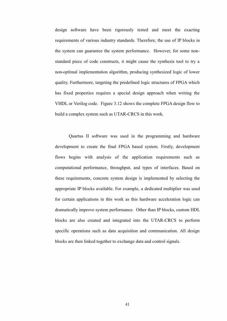
3.12 FPGA design flow 42
3.13 FPGA-based UTAR-CRCS architecture 45
3.14 Sonar range finder signal diagram 48
3.15 Flowchart of sonar range finder control signals generation 49
3.16 FSM in vehicle control module 50
3.17 FSM block for vehicle control in Quartus II 51
3.18 Part of VHDL code when FSM is in Forward state 51
3.19 Parallel communications between two blocks 53

xi
3.20 Low-level vehicle control module in UTAR-CRCS 54
3.21 SPI block that communicates with external DAC 56
3.22 UTAR-CRCS clock management 57
3.23 Frequency divider by factor of two 58
4.1 TRDB_D5M colour camera 62
4.2 Block diagram of TRDB_D5M reference design 64
4.3 UTAR-CRCS real-time image processing block diagram 65
4.4 3 x 3 convolution kernels on pixel P5 66
4.5 SIMD streams architecture 68
4.6 FPGA based Sobel operator implementation 69
4.7 Verilog code to initiate the multiplier-adder computations of
three line data with three ALTMULT_ADD blocks in X-
direction 70
4.8 Verilog code to initiate the parallel adder computations 70
4.9 Verilog code to initiate the square root functions 71
4.10 Line buffer implementation using ALTSHIFT_TAPS function 72
4.11 Sobel edge detection on real-time images 74
4.12 Time line diagram of processing activities on single frame of
image 75
4.13 Sample scene with tree trunks as obstacles and the detected
treetrunks in magenta 78
5.1 Vehicle control module FSM simulation 85
5.2 UTAR-CRCS system level simulation 87
5.3 Measured signals from DAC chips to DC motor controllers 91

xii
LIST OF ABBREVIATIONS
ACE Absolute contacting encoder
ALV Autonomous land vehicle
AUV Autonomous underwater vehicles
CPU Central processing unit
DAC Digital-to-analog converter
DARPA Defense Advanced Research Projects Agency
DSP Digital signal processor
FPGA Field programmable gate array
FSM Finite state machine
GPIO General purpose input/output
GPS Global positioning system
IP Intellectual property
LAGR Learning applied to ground robots
PWM Pulse width modulation
POMDP Partially observable Markov decision processes
RCS Real-time control system

xiii
SAUVIM Semi-autonomous underwater vehicle for
intervention missions
SDB Sensor data bus
SoC System on chip
SPI Serial peripheral interface
UGV Unmanned ground vehicle
UTAR-CRCS UTAR compact real-time control system
VGA Video graphic array

1
CHAPTER 1
INTRODUCTION
1.1 Research Motivation
Autonomous land vehicle (ALV) is a driverless vehicle with the
capability to navigate by itself using an intelligent control system. This
intelligent control system is to sense and perceive its surroundings necessary
to support navigational task. There are steady progresses made from the earlier
approach to current systems involving multiple sensors such as laser system,
stereovision, GPS, etc. Recent advance in sensors, communication, and
machine intelligence have made it possible to design more sophisticated ALV.
The potential applications of ALV range from daily life, search and
rescue mission to military. In recent years, global warming effects have
resulted in frequent disasters, such as: typhoon, hurricane, storms, etc. These
disasters have posted serious challenges to the search and rescue teams during
or after the disaster period. Some of the key issues are to react speedily to
reach the disaster/post-disaster locations by using autonomous vehicles; the
locations could have too narrow access for a typical autonomous vehicle
which has huge processing and control equipment on itself. The U.S.
Department of Defense (2010) published the 2009-2034 Unmanned System
Integrated Roadmap. In this roadmap, Special Operations Command

2
(SOCOM) is conducting a program that seeks to develop UGVs for
employment in reconnaissance, supply and protection missions for Special
Force units in forward operating situations. United States Northern Command
(NORTHCOM) and Pacific Command (PACOM) have both requested
technology development support for UGVs that can conduct tunnel
reconnaissance and mapping, and supply transport in complex terrain. To
overcome those challenges in a confined environment, compact autonomous
vehicle is needed. Thus, to minimize the control system becomes one of our
project objectives by using the-state-of-art solution.
With most RCS developed using multiple on-board CPUs and
microcontrollers, this research presents an alternative by using Field
Programmable Gate Array (FPGA) for the design and implementation of a
UTAR Compact Real-Time Control System (UTAR-CRCS) on an autonomous
vehicle. This will give the controller much better power in parallel computing
and flexible hardware modules reconfiguration by using programmable logic,
without an increase in size or costs.
The control system which was built on top of the Learning Applied to
Ground Robotics (LAGR) allows the unmanned vehicle to perform
autonomously in complex environments such as primitive forest trails (Alberts
et al., 2008). Rapid aging of civil and construction workers has led to the
development of M-2 which can carry construction materials and tools in the
field (Gomi, 2003). Japan‟s and USA‟s leading experts in rescue robotics are
deploying wheeled and snake-like robots to assist emergency responders in the
3
search for survivors of the devastating earthquake and tsunami that struck the
country in March, 2011.
Conventional ALV were designed to work in a known and well
protected environment such as office and lab. If this ALV is exposed to the real
world which is unknown to it, some service functions can still be provided but
many such attempts will eventually fail because of their lack of adaptability to
the dynamism of the real environment. In order to overcome all these
constraints, today, almost all ALV control system is RCS. In RCS, the present
state of the task activities sets the context that identifies the requirements for
all the support processing. RCS models complex real-time control through
sensory processing, internal world modelling and behaviour generation. These
3 components work together, receiving a task, and breaking it down into
simpler subtasks (Barbera et al., 2004).
Modern ALV with RCS can perform in a more satisfactory way though
not perfect. Many of these RCS are implemented on industrial PC such as PXI
together with different type of microcontrollers (Park et al., 2007). Due to
large amount of sensors and actuators to be monitored and controlled, RCS
system is developed using multiple on-board CPUs in order to solve the heavy
computational load (Kim & Yuh, 2004). These systems usually occupy a large
space that must be made available on the ALV. As a result, it will lead to
increase in size of autonomous vehicle and higher power consumption.

4
The autonomous operations deal with a lot of uncertainties when the
vehicle travels across the land. Although RCS is reasonably generalized and
has a multi-application system architecture, there is still room for increasing
the robustness of the architecture. RCS in its present form does not deal with
high uncertainty. Predictive navigation is integrated into RCS to improve the
effectiveness in performing worthwhile task. Seward et al. (2006) explained
how the use of Partially Observable Markov Decision Processes (POMDP)
can form the basis of decision making in the face of uncertainty and how the
technique can be effectively incorporated into the RCS architecture. The
computer based simulation has demonstrated that the POMDP technique can
be successfully integrated within a mobile robot controller and the resulting
autonomous behaviour is sensitive to variations in both the safety weighting
factor and the degree of uncertainty in sensor data. Widyotriatmo et al. (2009)
developed a predictive navigation through the extended Kalman filter (EKF)
algorithm to obtain a predicted area that might be occupied by a vehicle with
respect to particular input. By using reward value function, the vehicle has a
capability to cope with the problem of approaching object while also avoiding
obstacles.
The use of Field Programmable Gate Array (FPGA) as the control
platform for the autonomous vehicle can reduce the size of control platform on
the vehicle significantly. As a consequence, the vehicle can have extra space
for transportation. For example, vehicle can carry more basic necessities and
medical aid during the search and rescue mission. Furthermore, the
autonomous vehicle can be designed in a compact way so that it is more agile

5
when travelling autonomously. A compact design allows a better flexibility in
design and light-weight vehicle perform better in navigation across rough
terrain and has better maneuverability across obstacles (Tee & Tan, 2010). The
power consumption of the vehicle is also lower if FPGA is used as the control
platform. Using FPGA-based custom computing machines, Kentaro et al.
(2008) reported that the FPGAs perform the same computation with just 5 to
30 % of the total energy consumed by a microprocessor, while the FPGAs
accelerate the computation.
The era of SoC FPGA has just begun and roboticists have started to
show interests in using FPGA based control platform for autonomous vehicle.
A single FPGA device can work as microprocessors, microcontrollers, and
digital signal processing (DSP) devices. Murthy et al. (2008) demonstrated a
case study where FPGA based control system was derived and verified for a
simulated Unmanned Ground Vehicle (UGV). Besides that, system-on-chip
(SoC) using FPGA-based circuit board has also been designed to support
research and development of algorithms for image-directed navigation and
control (Wade & James, 2007). Table 1.1 shows some examples of SoC that
used FPGA as processing device in autonomous robot (Meng, 2006;
Mahyuddin, 2009). Among the applications, none of them demonstrates the
FPGA capability in autonomous control and vehicle navigation operations.
6
Table 1.1: Examples of SoC using FPGA as processing device
System on Chip
(SoC)
Year
Developed
Autonomous
Application Contributions
Helios
(Xilinx Virtex-4
FPGA)
2006 Small
autonomous
robot
3D reconstruction of an
environment using a
single camera (static
environment)
Moderate levels of
power consumption
Agent-based Mobile
Robot System
(Xilinx Virtex-2
FPGA)
2006 Pioneer 3DX
mobile robot Multi-agent based
architecture framework
Transport-independent
communication
mechanism for multi-
agent systems
Neuro-fuzzy based
Obstacle Avoidance
Program
(Altera Cyclone II
FPGA)
2009 Mobile robot Neuro-fuzzy based
obstacle avoidance
algorithm
The evolution of computing is toward parallelism, with the near-term
focus on processors shifting from higher, single-core processing power toward
multicore implementations. Both the advantages of parallel processing and the
increased number of gates have led to a rapid increase in popularity of FPGA
implementations. Seunghun et al. (2010) demonstrated a fully pipelined stereo
vision system providing dense disparity image with additional sub-pixel
accuracy in real-time. The hardware implementation is more than 230 times
faster when compared to a software program operating on a conventional
computer. The results show that FPGA based computing platform can also be
used to accelerate the signal processing for large amount of sensors and
actuators on the autonomous vehicle when compared to a conventional
computer.

7
1.2 Scope of Research
In this thesis, the research is focused on developing a compact real-time
control system which is named UTAR Compact Real-Time Control System
(UTAR-CRCS) for an autonomous vehicle. To achieve desired navigation,
high-level control of the system processes the data from all available sensors
and generates control signals to the low-level control of the vehicle.
The research questions addressed by this research are:
How to build a compact real-time control system of an autonomous
vehicle using a single FPGA device which works as microprocessors,
microcontrollers, and digital signal processor?
How to utilize the parallel processing technology on FPGA to accelerate
the processing of data from various kinds of sensors and navigation
decision making on the vehicle? This includes the vision data from on-
board camera.
The objectives of this research are:
To realize the parallelization of real-time autonomous vehicle control
architecture using FPGA technology
8
To develop the real-time Sobel edge detection module for the
autonomous vehicle control system using hardware programming
technology
To minimize and demonstrate the control system size-to-vehicle ratio
by using Altera DE1 board
1.3 Thesis Outline
Chapter 2 presents the literature review on the RCS of autonomous
vehicle. Most of the discussions are focused on the hardware and software of
control system, whereby the contributions and limitations of each control
system is highlighted.
Chapter 3 shows the development of UTAR-CRCS with the hardware
selection, system design methodology using Quartus II, and implementation
on Altera DE1 board. It includes the most important design considerations
that focus on system architecture, module specifications, and communication.
Chapter 4 explains and demonstrates the direct hardware
implementation of Sobel edge detector on real-time image from a camera
module. It shows the design and implementation that can accelerate the
computation speed and compares the performance to a high specification PC
based system.

9
Chapter 5 discusses about the simulations and measurement results.
The simulation waveforms on the system are presented, followed by the
measurements on the system performance. The UTAR-CRCS is also compared
to multiple CPUs system and the advantages of using FPGA based system are
highlighted.
Finally, the conclusion of the thesis is presented in Chapter 6. The
implications and results are also summarized. Besides, some suggestions for
future works are presented.

10
CHAPTER 2
LITERATURE REVIEW
2.1 Overview
Autonomous vehicles have generated much interest in recent years due
to their ability to perform relatively difficult tasks in hazardous and remote
environments. These vehicles are usually equipped with various components
for actuation, sensing, and communication. Such components have become
increasingly sophisticated and self-contained. The control system built on the
vehicle must integrate and coordinate these components properly so that
vehicle is able to navigate autonomously with minimal human intervention.
This section describes the work carried out in the area of control
system for autonomous vehicle, focusing on the hardware, software, and
control architecture used for the vehicle control. The contributions and
limitations of each system will be highlighted while the justification of using
FPGA as a control system in this thesis will be given.

11
2.2 Review of Control System for Autonomous Vehicle
RCS is one of the most popular control methodology employed in
autonomous vehicle. It is a reference model architecture that defines the types
of functions that are required in a real-time intelligent control system, and how
these functions are related to each other. Today, most RCSs are implemented
on central processing units (CPUs) or custom made industrial computers such
as PXI system provided by National Instrument.
2.2.1 Control System on LAGR for Unstructured Terrain
The Learning Applied to Ground Robotics (LAGR) program is a
Defense Advanced Research Projects Agency (DARPA) program that has the
goal of researching learning techniques in robot navigation. DARPA selected
certain research teams for LAGR program. Each LAGR robot is built on an
electric wheelchair platform with two pairs of bumblebee cameras for vision
and an on-board GPS antenna for global localization. In order to handle the
heavy computational load from the sensors and navigational planning, the
newer version of LAGR has three dual-core 2.0-Ghz Pentium-M based
computers. One computer is connected to the left camera pair, one to the right
camera pair, and one is for general use (Sermanet et al., 2009).
The University of Idaho (UI) LAGR Planner (UILP) and the UI
software for LAGR Vision (UILV) systems both use fuzzy logic as a tool for

12
creating logical outputs to complex systems (Alberts et al., 2008). The UILP
system contains two subsystems, the global path planner that determines a
route to final goal location and the local trajectory planner that creates the
translational and rotational drive commands. Global planner used a D*
algorithm (Stentz, 1994) on the global cost map of traversability costs. The
local planner uses a predictive controller to simulate possible routes and
maximizes performance of the trajectory based on the lowest cost route that
has the most confidence. For UILV, the system relies on Stanford Research
Institute (SRI) stereo vision libraries to compute depth images of the terrain.
Several courses were implemented to test the functionality of all the
aspects of the UI LAGR (UIL) system. The original intent was to compare
performance of the UIL system with the baseline system, but the unstructured
course turned out to be too difficult for the baseline system to navigate.
Overall, the baseline system followed a more direct route and collided with
more obstacles than UIL system. In contrast, the UIL system was successful
on all runs of the courses. UIL significantly improve the capabilities of the
LAGR robot and more importantly, allow it to perform autonomously in
complex environments such as primitive forest trails which include multiple
obstacles that the base system could not navigate.
Sermanet et al. (2009) developed a complete and robust software
navigation system providing collision-free and long-range navigation
capabilities for LAGR robots. Key to robust performance under uncertainty is
the combination of a short-range perception system operating at high frame
13
rate and low resolution and a long-range, adaptive vision system operating at
lower frame rate and higher resolution. The short-range module performs local
planning and obstacle avoidance with fast reaction times, while the long-range
module performs strategic visual planning.
Multi-layer perception, mapping and planning architecture handles the
latency and frequency issues by sophisticated processing. Depending on the
speed of the vehicle, the processing time and maximum distance of each
module, a balance between each module must be found to insure good results.
Maneuver dictionary and visual odometry contributed to the robust real-time
navigation due to their simplicity and efficiency. The complete system shows a
systematic performance improvement through various field tests over the
reference baseline system.
LAGR robot comes equipped with baseline software for autonomous
navigation. Over the years, the focus of LAGR program is on algorithm
development rather than be consumed early in the project with getting a
baseline robotic platform working. Thus, all work done on the robot is on high
level systems that address problems such as processing visual information and
adjusting to a changing environment. The actual hardware and low-level
software controllers are closed systems that cannot be altered by any of the
teams. There is always room for improvement in image processing. Asano et
al. (2009) showed that quad-core CPU can execute about 1/10 operations of
FPGA in a unit time. With a latest FPGA board with DDR-II RAM and a
larger FPGA, it is possible to double the performance by processing twice the

14
number of pixels in parallel.
2.2.2 Control System on SAUVIM
The need for autonomous underwater vehicles (AUV) for intervention
missions becomes greater as they can perform underwater tasks requiring
physical contacts with the underwater environment, such as underwater
construction and repair, cable streaming and mine hunting. Kim and Yuh
(2004) developed a semi-autonomous underwater vehicle for intervention
missions (SAUVIM) that has multiple on-board CPUs, redundant sensors and
actuators, on-board power source and a robot manipulator for dextrous
underwater performance. Such a complex robotic vehicle system requires
advanced control software architecture for on-board intelligence, making it to
have prompt response from high-level control with respect to low-level sensor
data.
SAUVIM was developed by the autonomous systems laboratory of the
University of Hawaii. The SAUVIM hardware has distributed architecture in
which processing nodes are connected through Ethernet and VME-bus for soft
real-time and hard real-time tasks. There are three MC68060-based CPU
boards that handle all operations of navigation module and robot manipulator.
Five additional Pentium-based PC/104+ CPU boards are used for sensor data
processing that often becomes heavy computational loads, such as image
processing for CCD cameras and scanning sonar. Besides, various analog and

15
digital I/O boards are used for interfacing with input sensors and output
actuators. The frequency bandwidth of the arm controller is programmable in
the range of 100 Hz to 1 kHz, while the vehicle is determined to be about 3-10
Hz. A higher bandwidth implies the potential of a control system to realize
faster motions.
The SAUVIM control software architecture is a sensor data bus based
control architecture (SDBCA) that has a modular, flexible structure for any
modification or additions. Thus, almost all of the software modules can be
easily rebuilt or replaced for upgrading or testing just like hardware
components. The overall architecture consists of three layers, application layer,
real-time layer and device layer. Application layer consists of application
software which is a sub-task module that includes all software modules for
high- and mid-level processing. The real-time layer consists of system
configurator, a real-time operating system, and some parts of sub-task modules.
Device layer is the only hardware dependent part that directly connects to
hardware to send command data for actuators and to obtain actual data from
sensors.
While the hierarchical architecture described is easy for verifying the
controllability and stability, it presents a lack of flexibility and a long response
time due to no direct communication between high-level control and low-level
peripherals. To overcome these disadvantages, a sensor data bus (SDB) is used
to supply a direct communication channel between low-, mid-, and high-level
layers. With SDB, urgent sensor signals can be handled in real-time and other
16
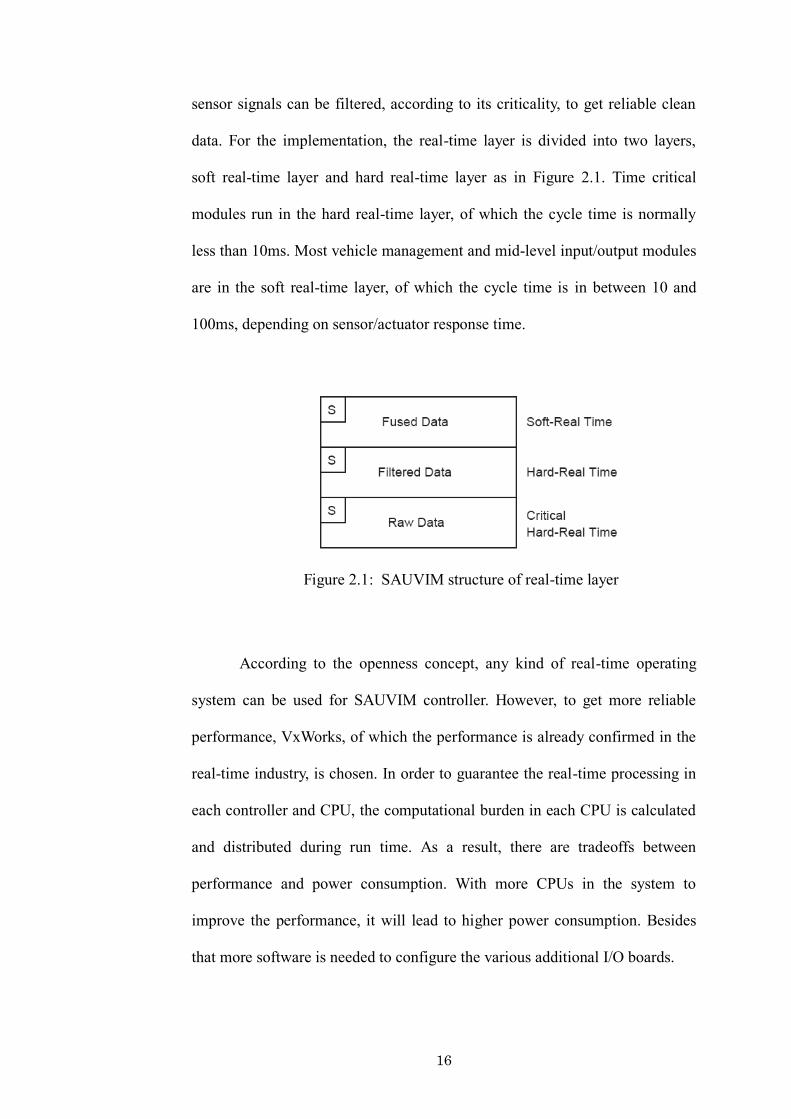
sensor signals can be filtered, according to its criticality, to get reliable clean
data. For the implementation, the real-time layer is divided into two layers,
soft real-time layer and hard real-time layer as in Figure 2.1. Time critical
modules run in the hard real-time layer, of which the cycle time is normally
less than 10ms. Most vehicle management and mid-level input/output modules
are in the soft real-time layer, of which the cycle time is in between 10 and
100ms, depending on sensor/actuator response time.
Figure 2.1: SAUVIM structure of real-time layer
According to the openness concept, any kind of real-time operating
system can be used for SAUVIM controller. However, to get more reliable
performance, VxWorks, of which the performance is already confirmed in the
real-time industry, is chosen. In order to guarantee the real-time processing in
each controller and CPU, the computational burden in each CPU is calculated
and distributed during run time. As a result, there are tradeoffs between
performance and power consumption. With more CPUs in the system to
improve the performance, it will lead to higher power consumption. Besides
that more software is needed to configure the various additional I/O boards.

17
2.2.3 Control System on ATRV
ATRV is a rugged four-wheel drive, differentially steered, all-terrain
robot vehicle for outdoor robotic research and application development. It is
stable in a wide variety of terrains and it can traverse them easily (Nebot et al.,
2011). An internal PC computer is installed in the vehicle with data and power
ports for user hardware interface. It is also equipped with a mobility object-
oriented software development environment.
The control architecture is one of the most important parts to develop
in a robotic system, especially if it is composed of several robots which must
cooperate. This control architecture must give support for all the facilities of
the systems and forms the backbone of the robotic system. Using ATRV as the
mobile robots, new control architecture is introduced for group of robots in
charge of doing maintenance tasks in agriculture environment. High Level
Architecture (HLA) can be considered the most important part because it not
only allows the data distribution and implicit communication among parts of
the system but also allows simultaneous operation with simulated and real
entities. The main objective of HLA is to create systems based on reusable
components of different nature which can interact easily through a distributed,
real-time operating system. HLA architecture must obey a set of rules and
interface specifications in order to govern the overall system and to govern
each participating component.
18
A robot must detect features in the sensory data stream that are salient
to the task in order to be successful in task execution. Behaviour-based robots
in particular use salient features to construct and sequence behaviours. The
salient features are extracted from sensory-motor sequences for mobile robot
navigation via teleoperation (Peng & Peters, 2005). During an offline
association step, sensory-motor sequences are partitioned into episodes
according to changes in motor commands. Salient features are then extracted
by using two statistical criteria: consistency and correlation with the motor
commands within the episode boundaries. The robot is controlled onboard by
a standard AMD Athlon XP 1.4GHz PC running Linux. All low-level sensing
and actuation modules run on the onboard computer. High-level modules and
user interface are executed on a remote laptop computer.
2.2.4 Control System on DEMO III
The US Department of Defense through its various agencies has been
major sponsor of research in autonomous vehicle. Notable examples include
the DEMO I, II, and III projects. The computing system includes a number of
Motorola CPU cards (MVME172, 2400, 2700) running VxWorks, which are
used for iris control, image acquisition, stereo vision, obstacle detection,
velocity control and terrain cover classification. A single PowerPC 750 is used
by the JPL stereo system to produce disparity maps at rate of 6 Hz (Belutta et
al., 2000).
19
Autonomous navigation in cross-country environments presents many
new challenges with respect to more traditional, urban environments. The lack
of highly structured components in the scene complicates the design of even
basic functionalities such as obstacle detection. Manduchi et al. (2005) had
developed a new sensor processing algorithm on DEMO III control system
that is suitable for cross-country autonomous navigation. Two approaches
were presented to obtain terrain cover perception, one based on stereo and
colour analysis, and the other based on range data processing. The algorithm
was ported to C++ and ran under VxWorks in a Pentium 4, 2.2 Ghz machine.
These techniques are at the core of JPL‟s perceptual system for autonomous
off-road navigation and have been tested in the context of several projects
funded by the US Department of Defense.
The RCS methodology and hierarchical task decomposition
architecture has been used to implement a number of diverse intelligent
control systems on DEMO III. Tests were conducted under various conditions
including night, day, clear weather, rain, and falling snow. The unmanned
vehicles operated over 90% of both time and distance without any operator
assistance. However, it should be noted that DEMO III tests were performed in
environments devoid of moving objects. The inclusion of moving objects in
the development of perception, world modelling, and planning algorithms for
operating an autonomous robot remains a challenging topic of current research.
As such, a description of the use of the task-decomposition-oriented RCS
methodology as an approach to acquiring and structuring the knowledge
required for the implementation of real-time complex control tasks was

20
presented (Barbera et al., 2004).
Figure 2.2: The basic internal structure of a RCS control loop
Figure 2.2 shows the basic structure of a RCS control loop. The hope is
that ontology tools and techniques will provide more consistent single
representational solution to capturing the knowledge and all the implied
relationships, especially to the task, in a more computer readable and
processible form.
2.3 Challenges in Compact Real-Time Control System
The preceding sections have briefly discussed the control system of
various autonomous vehicles, with their achievements and limitations, as
listed in Section 2.4 and Table 2.1.
With more sophisticated sensors and actuators used in a control system,
we anticipate more hardware resources to handle the heavy computational load.
21
Possibly the biggest challenge in a RCS is to improve the processing
capability while minimizing the power consumption. The integrity of RCS is
critical to ensure the system stability and performance in real-time
environment. It must assure continuity in system behaviour and output signals.
A failure in the system may result in material loss or even endanger human
lives. The following are some possible challenges in RCS for autonomous
vehicle.
1. A compact control system can minimize the system-to-vehicle
weight ratio and therefore is useful on a compact vehicle which can
travel across terrain, rainforest, and narrow tunnel. The light weight
control system will reduce the vehicle‟s weight significantly making
the vehicle more agile during navigation.
2. As RCS is getting more complex, parallel processing need to be
implemented in the RCS to accelerate the processing of data and
decision making. Otherwise, the system response will be slower and
real-time performance is not guaranteed.
In the Unmanned Ground Vehicle Integrated Roadmap (2010), the
research and development of small UGV for the future is clearly defined.
These small UGVs are expected to play more important roles in various kinds
of missions. It can assist the soldier with reconnaissance while aiding the
understanding and visualisation of the tactical picture. An advanced small
UGV is capable of operating on all terrains such as mud, sand, rubble-type
obstacles, 6-inch deep water, and in all weather conditions. Besides ground

22
operations, there is also continuous effort to develop and demonstrate a
marinized, small UGV to support at-sea maritime interdiction operations
including boarding and inspection of vessels of all sizes. Some of the UGVs
are available now and future modifications to them will result in more
sophisticated UGVs. iRobot is developing a Small Unmanned Ground Vehicle
(SUGV) which will weigh less than 13.6 kg for military use. The SUGV is
battery-operated and capable of conducting 6-hour missions in tunnel, sewers,
caves, and military operations in urban terrain areas.
Anthony and Steve (2010) also explained the developments and
challenges for autonomous vehicle. Primitive levels of autonomy are likely to
advance very rapidly once established; as soon as any relevant techniques are
developed and stable, they may be copied and run on smaller and cheaper
processor. In addition, unmanned ground vehicle do not require humans to be
onboard and consequently do not need any life support systems, space for
humans, special armour or protection. As a result, the vehicle can be made
smaller and lighter than their manned counterparts. As the procurement cost of
vehicles is roughly proportional to their mass, a reduction in mass can be
expected to translate into cost savings and a commensurate drop in the support
required for the vehicle. The continued drive for cost effectiveness, the
pressure for smaller operator footprints, and the capacity for cooperatives of
multiple unmanned vehicles to accomplish tasks that are difficult or
impossible for single unmanned vehicle have all combined to increase interest
in networks of smaller unmanned vehicles with increased automation. A
smaller unmanned vehicle needs a compact RCS.
23
2.4 Summary
This chapter reviews the control architecture, hardware and software
used in several existent control systems of various autonomous vehicles.
Table 2.1 shows the summary of control systems for various autonomous
vehicles. Their contributions are noted and limitations of the control system
are addressed. The need for a compact control system with parallel processing
capability is stressed. Finally, the challenges in the development of a real-time
control system and the need for compact RCS in small unmanned autonomous
vehicle are identified.

24
Table 2.1: Summary of control systems for various autonomous vehicles
Vehicle Author System
Architecture/Features Hardware Software Advantages Disadvantages
LA
GR
Sermanet
et al.
(2009)
1) Multi-layered
mapping, planning,
and command
execution system
2) Combination of
short-range perception
system and long-range
adaptive vision system
1) Three
dual-core
2.0-Ghz
Pentium-M
based
computers
2) Global
Positioning
System
(GPS)
3) Two pairs
of
bumblebee
cameras
4) Inertia
Measurement
Unit (IMU)
5) Wheel
encoders
Baseline
software
(based on
RANGER
system) for
autonomous
navigation
developed
by CMU's
Robotic
Institute.
1) This system
includes all the
necessary
hardware, sensors
and software to
create standard
development
environment.
2) NREC provides
remote technical
support, spare
parts supply and
user training.
1) Actual
hardware and
low-level
software are
closed systems
that can‟t be
altered by any
teams.
2) Multiple CPUs
in the system
occupy more
space and lead to
higher power
consumption
Alberts
et al.
(2008)
1) UILP and UILV
systems both use fuzzy
logic as a tool for
creating logical
outputs.
2) Predictive controller
to simulate possible
routes and maximizes
performance
25
Table 2.1 continued
Vehicle Author System
Architecture/Features Hardware Software Advantages Disadvantages
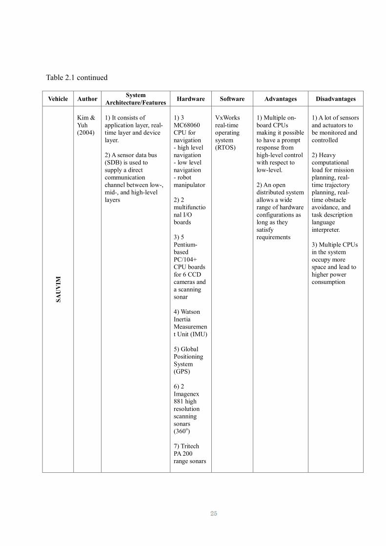
SA
UV
IM
Kim &
Yuh
(2004)
1) It consists of
application layer, real-
time layer and device
layer.
2) A sensor data bus
(SDB) is used to
supply a direct
communication
channel between low-,
mid-, and high-level
layers
1) 3
MC68060
CPU for
navigation
- high level
navigation
- low level
navigation
- robot
manipulator
2) 2
multifunctio
nal I/O
boards
3) 5
Pentium-
based
PC/104+
CPU boards
for 6 CCD
cameras and
a scanning
sonar
4) Watson
Inertia
Measuremen
t Unit (IMU)
5) Global
Positioning
System
(GPS)
6) 2
Imagenex
881 high
resolution
scanning
sonars
(360o)
7) Tritech
PA 200
range sonars
VxWorks
real-time
operating
system
(RTOS)
1) Multiple on-
board CPUs
making it possible
to have a prompt
response from
high-level control
with respect to
low-level.
2) An open
distributed system
allows a wide
range of hardware
configurations as
long as they
satisfy
requirements
1) A lot of sensors
and actuators to
be monitored and
controlled
2) Heavy
computational
load for mission
planning, real-
time trajectory
planning, real-
time obstacle
avoidance, and
task description
language
interpreter.
3) Multiple CPUs
in the system
occupy more
space and lead to
higher power
consumption

26
Table 2.1 continued
Vehicle Author System
Architecture/Features Hardware Software Advantages Disadvantages
DE
MO
III
Manduc
hi et al.
(2005)
1) New sensor
processing algorithm
on control system that
is suitable for cross-
country autonomous
navigation.
1) Multiple
Motorola
CPU cards
(MVME172,
2400, 2700)
2) LADAR
3) RADAR
4) Color
cameras
VxWorks
real-time
operating
system
(RTOS)
1) Multiple on-
board CPUs
dedicated to
individual sensor
speed up the
processing of data
1) Multiple CPUs
in the system
occupy more
space and lead to
higher power
consumption
Barbera
et al.
(2004)
1) RCS methodology
and hierarchical task
decomposition
architecture
2) Consistent single
representational
solution to capturing
the knowledge and all
the implied
relationships
1) It has a world
model that caters
for different real-
time situations.
2) It decomposes
tasks into
subtasks where
each control
module is
concerned with
only its own level
of responsibility
in the
decomposition of
the task.
1) It needs a huge
database for
world modelling.
2) Complex
control structure
and algorithm.
Un
man
ned
Veh
icle
Park et
al.
(2007)
1) The system consists
of Host, RT Target &
Obstacle detection
2) Navigation and
vehicle control in RT
target
1) 3 PXIs,
industrial
computer as
host PC, RT
target and
obstacle
detecting
system.
2) DC motor
48 V, 2.2
kW/3 HP to
drive
vehicle.
3) AC servo
motor to
control drum
type brake
and steering.
4) Laser
scanners &
color
cameras
1) NI DAQ
& NI motion
2) Windows
XP
Professional
1) It shows better
results than the
previous system
where response
time is shorter.
2) 2 degree
freedom for easy
computation
process.
1) Bulky control
system on
vehicle: 3 PXIs
for processing
2) Still under
development and
not yet reach
stable operation.
27
Table 2.1 continued
Vehicle Author System
Architecture/Features Hardware Software Advantages Disadvantages
AT
RV
Nebot
et al.
(2011)
1) High Level
Architecture (HLA)
generates systems
based on reusable
components of
different nature which
can interact among
them easily through a
distributed, real-time
operating system
1) Pentium
based
computers /
AMD
Athlon XP
based
computers
2) Global
Positioning
System
(GPS)
3)Sony color
camera
4) Inertia
Measuremen
t Unit (IMU)
5) Wheel
encoders
6) SICK
Laser
1) Linux
1) This system
includes all the
necessary
hardware, sensors
and software to
create standard
development
environment.
1) Multiple CPUs
in the system
occupy more
space and lead to
higher power
consumption
Peng &
Peters
(2005)
1) Salient features are
extracted from the
offline data association
to construct and
sequence the vehicle's
behaviours

28
CHAPTER 3
UTAR COMPACT REAL-TIME CONTROL SYSTEM (UTAR-CRCS)
3.1 Overview
Real-time (RT) systems are defined as those systems in which the
correctness of the system depends not only on the logical result of
computations, but also on the time at which the results are produced. The most
characteristic misconception in the domain of real-time systems is that real-
time computing is often considered as fast computing (Colnaric et al., 1998). It
must be understood that computer speed itself cannot guarantee that specific
timing requirements will be met. Instead, being able to assure that a process
will be completed within a predefined time frame is of utmost importance. In
RCS, if the timing requirements are not met or the task response action is
delayed for any reason, a catastrophic failure might occur. For the task-
specific controller described in this work, if the task response-time
requirements are not met, the vehicle controller will not be able to provide a
stable control action. In general, the main characteristics of RCS are:
1. Able to process multiple tasks in parallel
2. Predictability of temporal behaviour and continuity in output signals
3. Meet timing deadlines for the processes

29
Based on the previous literature review, it is clear that in most of the
research done, RCSs are built using multiple PCs, microcontrollers, and digital
signal processors. In this work, the proposed Field Programmable Gate Array
(FPGA) based UTAR Compact Real-Time Control System (UTAR-CRCS)
overcomes some of the challenges in RCS for ALV.
3.2 UTAR-CRCS
The UTAR-CRCS system of an ALV is shown in Fig. 3.1. It consists of
a remote control system, navigation system, vehicle control system, and
multiple sensors that are connected to the system.
Figure 3.1: UTAR-CRCS control architecture

30
Navigation system is a high-level controller that performs obstacle
avoidance. ALV can sense its surrounding with the range sensors and this
information will be used for obstacle detection. Ultrasonic sensors are used in
this work and it can be set to detect obstacles in a desired distance. Infrared
(IR) sensor can also be used to sense range but it is easily influenced by
ambient light at outdoor environment. Thus, ultrasonic sensor is preferred over
IR sensor in the development of UTAR-CRCS. Besides, a colour camera is
used to acquire real-time image of the surrounding. The Global Positioning
System (GPS) will provide the location of the ALV on the earth. The trajectory
instructions are generated in this system and the control signals will be sent to
the vehicle control system. In case the ALV faces an indecisive situation, the
manual interaction will come into control where remote control system allows
a shift from autonomous to manual operation dynamically.
The vehicle control system is a low-level controller that performs
steering and driving tasks. It processes the signals from the navigation system,
and the rotary encoders and then generates control signals to the DC motors.
The rotary encoder will encode the speed of each DC motor and provide
feedback to the system for speed control. One of the key features in this vehicle
control system is zero-radius turning. The ALV is capable of a zero-radius turn
in a confined area such as a tunnel. Figure 3.2 shows the ALV that is installed
with the UTAR-CRCS.
31
Figure 3.2: ALV with the UTAR-CRCS
3.2.1 Hardware Description
This section describes the hardware used in the project reported in this
thesis to build the UTAR-CRCS. This includes the Altera DE1 Development
Board which is the processing platform for the control system. Generally, the
UTAR-CRCS consists of an embedded control system, a colour camera, low-
level sensors, and a custom built I/O board for interfacing with the DC motor
controller.

32
3.2.1.1 Altera DE1 Development Board
All the important components on the board are connected to pins of a
state-of-the-art Cyclone II 2C20 FPGA, allowing user to control all aspects of
the operation. Figure 3.3 shows the DE1 development board and Table 3.1
shows the DE1 board specification.
Figure 3.3: Altera DE1 development board
Table 3.1: Altera DE1 development board specification
Parameter DE1 Development Board
FPGA
Cyclone II EP2C20F484C7
EPCS4 serial configuration device
I/O Devices
Built-in USB Blaster for FPGA configuration
RS-232 port
VGA DAC resistor network (4096 colours)
PS/2 mouse or keyboard port
Line-in, line-out, microphone-in (24-bit audio CODEC)
Expansion headers (76 signals)
VGA Video
Port
Power Switch
On-Board
Oscillators
USB Blaster
Controller Chipset
7-SEG
Display
Toggle
Switches
GPIO Pins
RS-232 Port
Cyclone II
FPGA
Push Button
Switches
SDRAM

33
Memory
8-MB SDRAM
512-KB SRAM
4-MB Flash
SD memory card slot
Switches, LEDs,
Displays, and Clocks
10 toggle switches
4 debounced pushbutton switches
10 red LEDs, 8 green LEDs
Four 7-segment displays
27-MHz and 50-MHz oscillators
The VGA port on the board is connected to an LCD monitor for real-
time image display while SDRAM is used as a buffer for input image data
before output for display. The GPS receiver module communicates with the
DE1 board though the RS-232 port. On the board, general purpose I/O in
expansion headers are used to interface with external hardware which includes
various sensors, DC motor controllers, and the remote control receiver. The
I/O pins can also be optionally connected to LEDs to provide a visual
indicator of processing activity. Both 27 and 50 MHz oscillators are used as
system clocks.
3.2.1.2 Global Positioning System (GPS)
The Fastrax UC322 is an OEM GPS receiver module which
provides low power 90 mW operation together with weak signal
34
acquisition and tracking capability to meet even the most stringent
performance expectations. This module provides complete signal
processing from an embedded GPS antenna to serial data output in
NMEA message. Figure 3.4 shows the GPS receiver.
Figure 3.4: Fastrax UC322 GPS receiver
3.2.1.3 Sonar Range Finder
MaxSonar-EZ1 detects objects from 0-inch to 254-inches with 1-
inch resolution. It is installed on the ALV for obstacle detection. The
interface output formats included are pulse width output, analog voltage
output, and serial digital output. In this work, pulse width output is used
as input to DE1 board which then encodes the range finder‟s reading.
After that, the values are sent to the navigation module for further
processing. Figure 3.5 shows the sonar range finder.
Antenna
Processing Unit

35
Figure 3.5: MaxSonar-EZ1 sonar range finder
In order to process the pulse width (PW) input and decode the sensed
distance value, the following expressions were used:
PW = Count x (1/fclk) 3.1
Distance = (PW / 147 us) x 0.0254 m 3.2
where 147 us in Eq. 3.2 represents 0.0254 m. All these computations were
implemented using floating point multiplier and divider IP blocks.
3.2.1.4 Rotary Encoder
RE08A is a rotary encoder which comes with a slotted disc (8 slots)
and a simple interface sensor board. The sensor converts the data of rotary
motion into a series of electrical pulses. The electrical pulses are then counted
by the digital counter in the control system. With this concept, the rotary
encoder is employed in the DC motor shaft so that the controller can sense the
current motor speed as shown in Figure 3.6.
Transceiver Processing Unit
36
Figure 3.6: RE08A rotary encoder
3.2.1.5 Bourns Absolute Contacting Encoder (ACE)
Bourns ACE is an intelligent alternative to incremental encoders and
potentiometers. Through the use of combinatorial mathematics, the gray-code
pattern provides an absolute digital output that will also retain its last position
in the event of a power failure. It is installed on the rear wheels to sense the
orientation of rear wheels under different operations, especially in positioning
the rear wheels for zero radius turn. Figure 3.7 shows the Bourns ACE.
Figure 3.7: Bourns absolute contacting encoder
Optical Sensor
Slotted Disc
I/O Pins
I/O Pins
Shaft
37
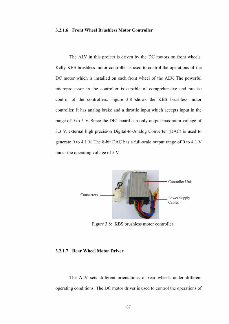
3.2.1.6 Front Wheel Brushless Motor Controller
The ALV in this project is driven by the DC motors on front wheels.
Kelly KBS brushless motor controller is used to control the operations of the
DC motor which is installed on each front wheel of the ALV. The powerful
microprocessor in the controller is capable of comprehensive and precise
control of the controllers. Figure 3.8 shows the KBS brushless motor
controller. It has analog brake and a throttle input which accepts input in the
range of 0 to 5 V. Since the DE1 board can only output maximum voltage of
3.3 V, external high precision Digital-to-Analog Converter (DAC) is used to
generate 0 to 4.1 V. The 8-bit DAC has a full-scale output range of 0 to 4.1 V
under the operating voltage of 5 V.
Figure 3.8: KBS brushless motor controller
3.2.1.7 Rear Wheel Motor Driver
The ALV sets different orientations of rear wheels under different
operating conditions. The DC motor driver is used to control the operations of
Power Supply
Cables
Controller Unit
Connectors
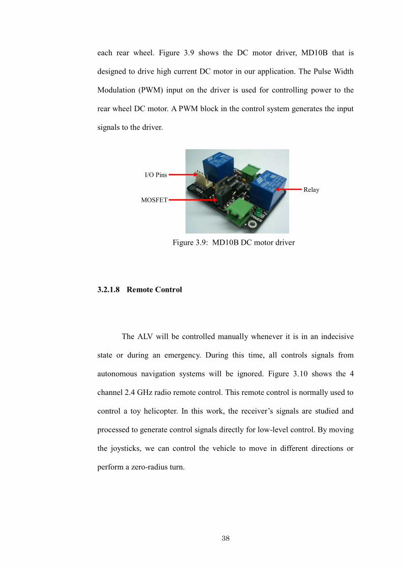
38
each rear wheel. Figure 3.9 shows the DC motor driver, MD10B that is
designed to drive high current DC motor in our application. The Pulse Width
Modulation (PWM) input on the driver is used for controlling power to the
rear wheel DC motor. A PWM block in the control system generates the input
signals to the driver.
Figure 3.9: MD10B DC motor driver
3.2.1.8 Remote Control
The ALV will be controlled manually whenever it is in an indecisive
state or during an emergency. During this time, all controls signals from
autonomous navigation systems will be ignored. Figure 3.10 shows the 4
channel 2.4 GHz radio remote control. This remote control is normally used to
control a toy helicopter. In this work, the receiver‟s signals are studied and
processed to generate control signals directly for low-level control. By moving
the joysticks, we can control the vehicle to move in different directions or
perform a zero-radius turn.
Relay
I/O Pins
MOSFET
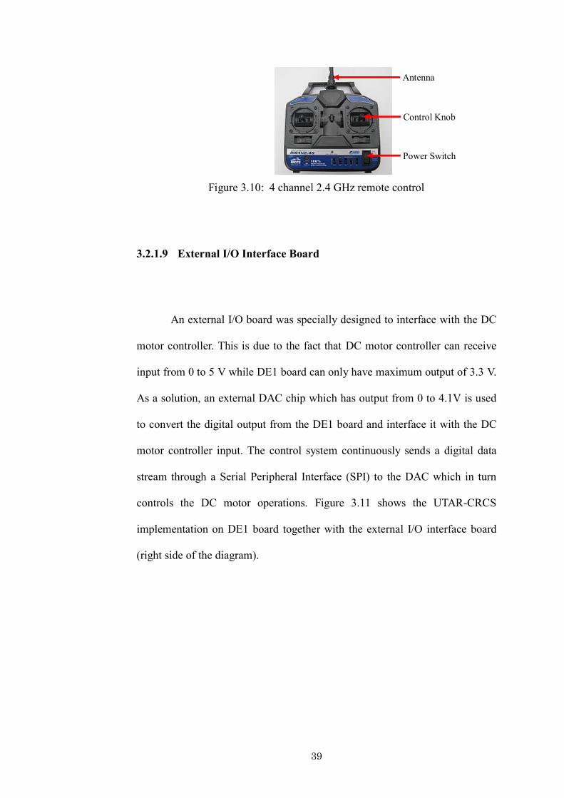
39
Figure 3.10: 4 channel 2.4 GHz remote control
3.2.1.9 External I/O Interface Board
An external I/O board was specially designed to interface with the DC
motor controller. This is due to the fact that DC motor controller can receive
input from 0 to 5 V while DE1 board can only have maximum output of 3.3 V.
As a solution, an external DAC chip which has output from 0 to 4.1V is used
to convert the digital output from the DE1 board and interface it with the DC
motor controller input. The control system continuously sends a digital data
stream through a Serial Peripheral Interface (SPI) to the DAC which in turn
controls the DC motor operations. Figure 3.11 shows the UTAR-CRCS
implementation on DE1 board together with the external I/O interface board
(right side of the diagram).
Control Knob
Power Switch
Antenna
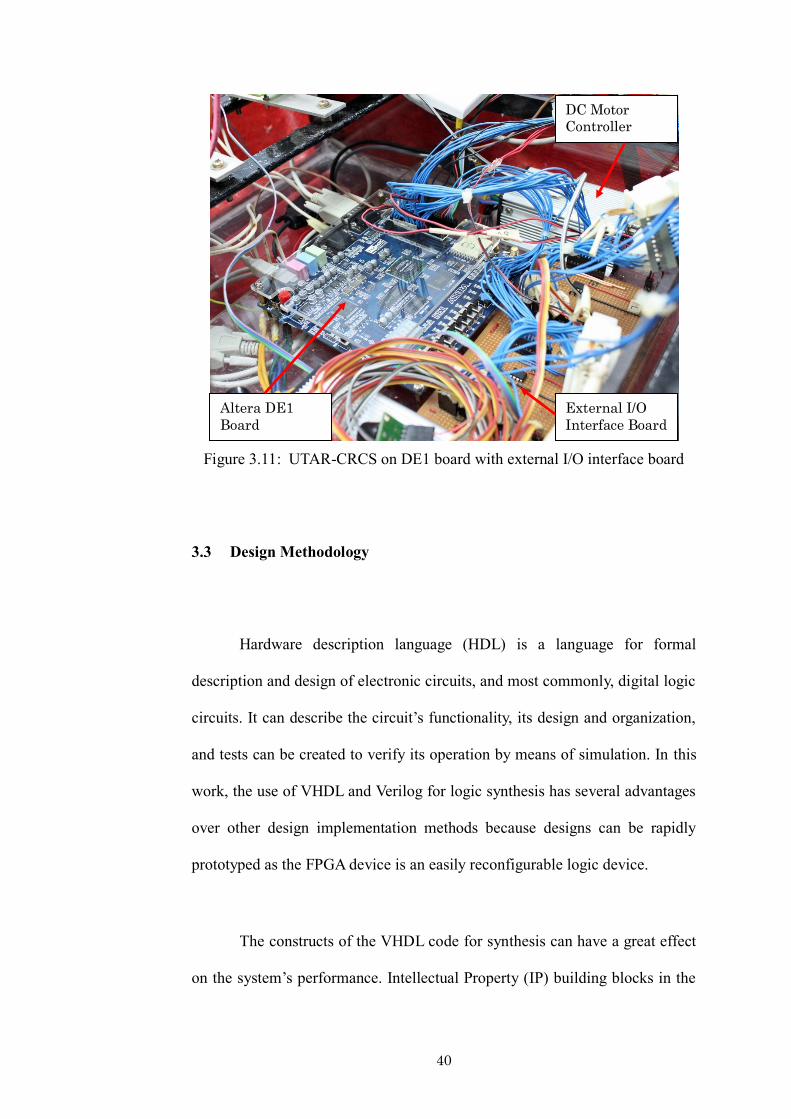
40
Figure 3.11: UTAR-CRCS on DE1 board with external I/O interface board
3.3 Design Methodology
Hardware description language (HDL) is a language for formal
description and design of electronic circuits, and most commonly, digital logic
circuits. It can describe the circuit‟s functionality, its design and organization,
and tests can be created to verify its operation by means of simulation. In this
work, the use of VHDL and Verilog for logic synthesis has several advantages
over other design implementation methods because designs can be rapidly
prototyped as the FPGA device is an easily reconfigurable logic device.
The constructs of the VHDL code for synthesis can have a great effect
on the system‟s performance. Intellectual Property (IP) building blocks in the
External I/O
Interface Board
Altera DE1
Board
DC Motor
Controller
41
design software have been rigorously tested and meet the exacting
requirements of various industry standards. Therefore, the use of IP blocks in
the system can guarantee the system performance. However, for some non-
standard piece of code constructs, it might cause the synthesis tool to try a
non-optimal implementation algorithm, producing synthesized logic of lower
quality. Furthermore, targeting the predefined logic structures of FPGA which
has fixed properties requires a special design approach when writing the
VHDL or Verilog code. Figure 3.12 shows the complete FPGA design flow to
build a complex system such as UTAR-CRCS in this work.
Quartus II software was used in the programming and hardware
development to create the final FPGA based system. Firstly, development
flows begins with analysis of the application requirements such as
computational performance, throughput, and types of interfaces. Based on
these requirements, concrete system design is implemented by selecting the
appropriate IP blocks available. For example, a dedicated multiplier was used
for certain applications in this work as this hardware acceleration logic can
dramatically improve system performance. Other than IP blocks, custom HDL
blocks are also created and integrated into the UTAR-CRCS to perform
specific operations such as data acquisition and communication. All design
blocks are then linked together to exchange data and control signals.
42
Figure 3.12: FPGA design flow
Using the Quartus II software, pin locations and other pin constraints
are applied for I/O signals. This is followed by compilation of the design that
provides a report file in the synthesis, fitter, map, placement, and assembler
stages. The report file provides useful information on the device configuration.
Besides report file, compilation also generates a SRAM Object File (.sof) that
can be downloaded to the FPGA device. After all this, the performance is
analyzed from various aspects such as functionalities, timing requirements and
stability. If improvement in the system is needed, design files can be modified
and updated.
A typical FPGA design flow normally requires simulation stage after
the project compilation. It is performed on the individual block itself and then

43
on the integrated system. The simulation can show the individual block or
system performance in terms of functionality and timing before
implementation. This stage is critical and must be performed before the
hardware implementation.
3.3.1 VHDL and Verilog Constructs for FPGA Logic Design
Table 3.2: VHDL and Verilog code for AND gate
VHDL Code Verilog Code
library ieee;
use ieee.std_logic_1164.all;
entity andgate is
port( x: in std_logic;
y: in std_logic;
F: out std_logic);
end andgate;
architecture behav of andgate is
begin
F <= x and y;
end behav;
module andgate (x, y, F);
input x, y;
output F;
assign F = x & y;
endmodule
This work used VHDL and Verilog as the design entry method, Table
3.2 shows the VHDL and Verilog code for an AND gate. A digital system in
VHDL consists of an entity that can contain other design entities which are
then considered as components of the top-level entity. The entity is modelled
by an entity declaration and an architecture body. Entity declaration is the
F x
y
44
interface to the external world that defines the input and output signals while
architecture body contains description of the entity and is composed of
interconnected entities, process and components, all operating concurrently. In
UTAR-CRCS, many entities are connected together to build the top-level
entity.
In Verilog, a circuit is represented by a set of modules. Referring to
Table 3.2, a module is a keyword and andgate is the name given to this module.
The module begins with declaration of all ports as input and output. It is then
followed by the description of the module that contains any combination of the
following: variable declaration, concurrent and sequential statement blocks,
and instances of other modules. Compared to Verilog, VHDL is more tedious
in coding for the same circuit. However, a structure can be modelled equally
effectively in both VHDL and Verilog. In this project, both VHDL and Verilog
are used because the author is more familiar with VHDL but there are some IP
blocks that were written in Verilog code.
3.4 UTAR-CRCS Implementation
UTAR-CRCS was designed and developed using Altera Quartus II
software. The design entry methods include Intellectual Property (IP) blocks,
custom VHDL and Verilog design. Simulations are performed for design
verification. The system was implemented on Altera DE1 boad that is installed
on an ALV. The following section will describe the FPGA-based design details.

45
3.4.1 FPGA-based System Architecture
The FPGA-based UTAR-CRCS is an embedded system as shown in
Figure 3.13. In this design, an FPGA device works as processing units,
microcontrollers and digital signal processors.
On-Chip System Interconnect
Sensors
Module
Camera
Module
GPS
Module
RF Receiver
CMOS
Camera
GPS
Receiver
Ultrasonic
Range
Sensors
DC Motor
Controller (Right)
DC Motor
Controller(Left)
DC Motor Speed
Encoder (Right)
DC Motor Speed
Encoder (Left)
VGA
Controller
LCD
Display
SDRAM
Controller
System
Clock
External
SDRAM
Cyclo
ne
II F
PG
A
Emergency
StopNavigation
Module
On-Chip System
Interconnect
RF Remote
Control
Remote Control
Module
Front Wheel
DC Motor
Driver (Right)
DC Motor
Driver (Left)
Absolute Encoder
(Right)
Absolute Encoder
(Left)
Rear Wheel
Vehicle Control Module
Figure 3.13: FPGA-based UTAR-CRCS architecture
This system consists of multiple modules that are interconnected to
each other using the on-chip system interconnect; coupling is achieved
through parallel links and control signals. The arrows between modules in the
diagram show clearly the direction of data flow or communication in the
system. In the UTAR-CRCS, system clocks come from the on-board 27 and 50
MHz oscillators. The clock signals are loaded to the modules based on
individual module requirement.

46
During real-time operation, all modules run concurrently and
according to Flynn‟s taxonomy, this is Multiple Instruction, Multiple Data
(MIMD) streams architecture. MIMD is a technique employed to achieve
parallelism so that at any time, different modules are executing different
instructions on different pieces of data. By moving towards multiple modules
for peripheral devices, high-level control modules are relieved from that work,
and peripheral services are much more flexible and fault tolerant.
Sensors provide two kinds of data: they acquire values of input
variables and notify the control system of events, which influence the further
process‟s behaviour. Typically, the control system senses system states,
characteristic values, data inputs and, with calculated results, controls the DC
motor controllers and drivers. The times to react to events are in the order of
magnitude of milliseconds, and must be guaranteed. The real-time vision
system was developed on another DE1 board due to insufficient I/O pins on a
single DE1 board; this vision system will be explained in details in Section 4.
As a result, the whole system architecture was implemented on 2 DE1 boards
and board-to-board communication is established through a UART.
3.4.2 Module Specifications
The structure of UTAR-CRCS depends on specification and
implementation issues. Controller functionality was specified and
implemented using modules and tasks. A module is a fixed part of the target
47
device whereas tasks represent the different signal processing functionalities
of a module. There can be more than one task loaded in a module thus
consuming more chip area. Specifications of module and task employ data
flow and control flow specification methods.
3.4.2.1 Data Flow
A task normally works on of multiple input and output data. In a task
processing, there is always a condition on when the input data should be
processed and when an acknowledgement signal should be sent out to the
subsequent task. The flow of data must be organized and set in orderly manner
to ensure that the system works accurately.
In UTAR-CRCS, data flow is controlled by various control signals that
flow through the task. Thus, data flow is specified by a signal diagram
showing clearly the events of input and output signals. To demonstrate the use
of signal diagram in controlling the data flow, Figure 3.14 shows the signal
diagram in reading a value from ultrasonic range sensor. Sonar_Request and
Sonar_Input are input signals while Sonar_ON and Data_Ready are output
signals for the task.

48
Figure 3.14: Sonar range finder signal diagram
When the control system needs to sense a distance, it sends a signal
(logic „high‟ in Sonar_Request) to the task. The task turns on (Sonar_ON is
asserted „high‟) the ultrasonic sensor, and sends an acknowledge signal
(Data_Ready is asserted „low‟) to subsequent task to indicate that the data is
not ready to be read. Next, the sensor input is processed and converted to a
fixed data format with an output latency of 10 clock cycles. After all this, an
acknowledge signal (Data_Ready is asserted „high‟) is sent to subsequent task
to indicate that the data is ready to be read. The output latency comes from
floating-point conversion and floating-point multiplication used to process the
input signal. Latency must be determined to ensure that all arithmetic
operations have been performed on the data before the output data is read.
The signal diagram provides a good graphical representation of the
signal flows which in turn controls the data flow. For implementation, a
flowchart is used as a step-by-step solution of HDL programming in Quartus
II to generate the control signals. Figure 3.15 shows the flowchart for the
signal diagram in Figure 3.14. In this case, different events of the sensor input
(Sonar_Input) are detected using conditional statements in the programming.
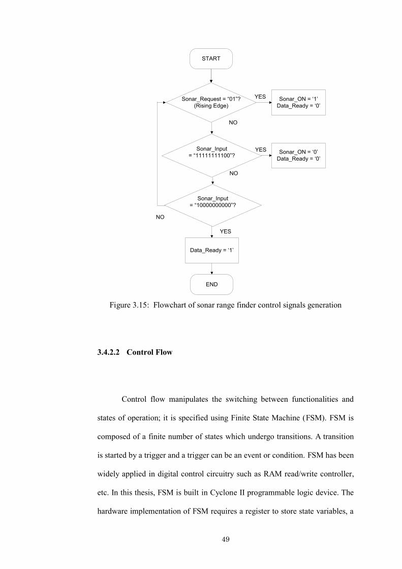
49
START
Sonar_ON = „1‟
Data_Ready = „0‟
Sonar_ON = „0‟
Data_Ready = „0‟
Data_Ready = „1‟
END
YES
NO
YES
YES
NO
NO
Sonar_Input
= “10000000000”?
Sonar_Request = “01”?
(Rising Edge)
Sonar_Input
= “11111111100”?
Figure 3.15: Flowchart of sonar range finder control signals generation
3.4.2.2 Control Flow
Control flow manipulates the switching between functionalities and
states of operation; it is specified using Finite State Machine (FSM). FSM is
composed of a finite number of states which undergo transitions. A transition
is started by a trigger and a trigger can be an event or condition. FSM has been
widely applied in digital control circuitry such as RAM read/write controller,
etc. In this thesis, FSM is built in Cyclone II programmable logic device. The
hardware implementation of FSM requires a register to store state variables, a

50
block of combinational logic which determines the state transitions, and a
second block of combinational logic that determines the outputs of the FSM.
Moore machine is an FSM whose output values are determined solely
by its current state. Figure 3.16 shows an example of an FSM used in vehicle
control modules. It controls the operations of a DC motor controller that drives
the front wheel. This special FSM consists of 5 states and each of the states
represents a single task of the module that has to be loaded on certain
conditions. . In this case, output calculation depends on the state vector which
means new values are stable long before the next active clock edge and spikes
are avoided. The input in this FSM is FRB which represents Forward, Reverse
and Brake control signals.
Figure 3.16: FSM in vehicle control module
Figure 3.17 shows the FSM block, motor_control_FSM in vehicle
control, with its inputs and outputs in Quartus II. At each of the output state,

51
the subsequent block will read the state value and generate the control signals
in the vehicle control module which in turn controls the DC motor operations.
The control mechanism was coded using VHDL. Figure 3.18 shows a part of
the VHDL code when the FSM is in Forward state. If the input FRB is “100”,
next state (NS) will be forward (F). Else, FSM will jump to Clear Throttle
(CA) as next state.
Figure 3.17: FSM block for vehicle control in Quartus II
when F =>
if (SS_DETECT_TEMP = "000111") then
if (FRB = "100") then
NS <= F;
else
NS <= CA;
end if;
else
NS <= F;
end if;
Figure 3.18: Part of VHDL code when FSM is in Forward state
This FSM ensures a safe operation of the vehicle because any accident
arising from improper control of the DC motor will cause harm to the
environment and endanger human life. Besides safety issues, the FSM in this
work is also developed according to the DC motor controller specifications.
For example, the DC motor can rotate in both forward and reverse direction;

52
previous input value for speed must be cleared before the change in direction.
So, FSM is employed to guarantee a smooth transition between different states.
3.4.3 Communication
Data communications concerns the transmission of digital messages
between the modules in the system and from the system to external devices.
For the real-time control system in this work, both on-chip and off-chip
communication methods are established for data communication.
3.4.3.1 On-Chip
The distance over which data moves within a system may be a few
thousandths of an inch, as in the case within a single FPGA device. Over such
a small distances, digital data can be transmitted as a direct, two-level
electrical signal. Parallel links are widely used in modern designs for on-chip
inter-module communication since it is a high speed transmission of data;
many bits of data can be transmitted simultaneously at a time. Multiple
modules and tasks in UTAR-CRCS communicate through bit-level parallel
communication. Both synchronous and asynchronous transmission methods
are employed in parallel communication.
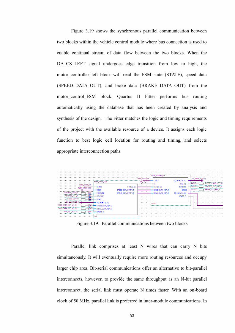
53
Figure 3.19 shows the synchronous parallel communication between
two blocks within the vehicle control module where bus connection is used to
enable continual stream of data flow between the two blocks. When the
DA_CS_LEFT signal undergoes edge transition from low to high, the
motor_controller_left block will read the FSM state (STATE), speed data
(SPEED_DATA_OUT), and brake data (BRAKE_DATA_OUT) from the
motor_control_FSM block. Quartus II Fitter performs bus routing
automatically using the database that has been created by analysis and
synthesis of the design. The Fitter matches the logic and timing requirements
of the project with the available resource of a device. It assigns each logic
function to best logic cell location for routing and timing, and selects
appropriate interconnection paths.
Figure 3.19: Parallel communications between two blocks
Parallel link comprises at least N wires that can carry N bits
simultaneously. It will eventually require more routing resources and occupy
larger chip area. Bit-serial communications offer an alternative to bit-parallel
interconnects, however, to provide the same throughput as an N-bit parallel
interconnect, the serial link must operate N times faster. With an on-board
clock of 50 MHz, parallel link is preferred in inter-module communications. In
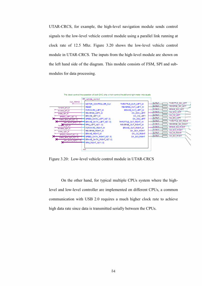
54
UTAR-CRCS, for example, the high-level navigation module sends control
signals to the low-level vehicle control module using a parallel link running at
clock rate of 12.5 Mhz. Figure 3.20 shows the low-level vehicle control
module in UTAR-CRCS. The inputs from the high-level module are shown on
the left hand side of the diagram. This module consists of FSM, SPI and sub-
modules for data processing.
Figure 3.20: Low-level vehicle control module in UTAR-CRCS
On the other hand, for typical multiple CPUs system where the high-
level and low-level controller are implemented on different CPUs, a common
communication with USB 2.0 requires a much higher clock rate to achieve
high data rate since data is transmitted serially between the CPUs.

55
3.4.3.2 Off-Chip
Off-chip communications include interfaces to external devices for
transferring of data. All communications from UTAR-CRCS to external
devices were implemented using the general purpose input/output (GPIO) pins
on the Altera DE1 board. This is a great advantage over multiple CPUs system
where a specific I/O interface card is needed to communicate with external
devices. In addition, the external I/O interface card also increases the size of
the multiple CPUs system. Table 3.3 shows various off-chip communication
methods used in the control system. Through off-chip communication, the
real-time control system sends command data to the external devices, for
example, to configure the operation mode of an ultrasonic sensor. Besides that,
control system also performs data acquisition on various external devices.
Table 3.3: UTAR-CRCS off-chip communications
External Device Communication with Control System
Colour Camera Parallel Communication
Global Positioning System (GPS) Universal Asynchronous
Receiver/Transmitter (UART)
Digital-to-Analog Converter (DAC) Serial Peripheral Interface (SPI)
Sonar Range Finder Serial Communication
Rotary Encoder Serial Communication
Absolute Contacting Encoder Parallel Communication
Brushless Motor Controller Parallel Communication
Motor Driver Serial Communication
Remote Control Parallel Communication

56
The off-chip communications were developed according to the
individual external hardware specifications. Serial communication is the most
widely used process of sending data in this thesis. In serial communication,
data is sent one bit at a time. Motor driver is one of the devices that
communicate with the control system serially. At any one time, only one bit
data is sent to the pulse width modulation (PWM) input pin to switch the on-
board MOSFET ON and OFF to further control the speed of motor. On the
other hand, parallel communication is used to interface with the vision system.
The colour camera sends 12-bit pixel data and other configuration data in
parallel mode to the DE1 board through the GPIO pins.
The real-time control system needs a digital-to-analog converter
(DAC) for controlling the DC motor. However, today‟s FPGA lacks any on-
chip DAC conversion. Due to this problem, an off-chip 8-bit DAC component
is used and this device is Serial Peripheral Interface (SPI) compatible.
Therefore, the control system communicates with the DAC in master/slave
mode where the control system initiates the data frame. Figure 3.21 shows the
SPI block that communicates with external DAC chip, which controls DC
motor speed on the left front wheel.
Figure 3.21: SPI block that communicates with external DAC
Control signals and
data to external DAC
Processed data to be
transmitted through SPI
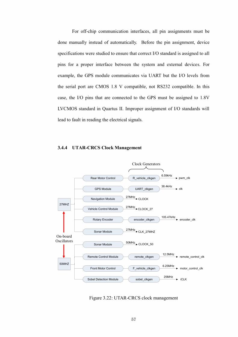
57
For off-chip communication interfaces, all pin assignments must be
done manually instead of automatically. Before the pin assignment, device
specifications were studied to ensure that correct I/O standard is assigned to all
pins for a proper interface between the system and external devices. For
example, the GPS module communicates via UART but the I/O levels from
the serial port are CMOS 1.8 V compatible, not RS232 compatible. In this
case, the I/O pins that are connected to the GPS must be assigned to 1.8V
LVCMOS standard in Quartus II. Improper assignment of I/O standards will
lead to fault in reading the electrical signals.
3.4.4 UTAR-CRCS Clock Management
27MHZ
50MHZ
GPS Module UART_clkgen38.4kHz
clk
Navigation Module27MHz
CLOCK
Rotary Encoder encoder_clkgen105.47kHz
encoder_clk
Sonar Module27MHz
CLK_27MHZ
Sonar Module50MHz
CLOCK_50
Remote Control Module remote_clkgen12.5MHz
remote_control_clk
Front Motor Control F_vehicle_clkgen6.25MHz
motor_control_clk
Rear Motor Control R_vehicle_clkgen6.59kHz
pwm_clk
Vehicle Control Module27MHz
CLOCK_27
Sobel Detection Module sobel_clkgen25MHz
iCLK
Figure 3.22: UTAR-CRCS clock management
On-board
Oscillators
Clock Generators
58
UTAR-CRCS requires different clock speed for various processing
needs in the system. Figure 3.22 shows the clock diagram for different
modules. There are some applications in the system that require lower clock
speed, for example, the rear motor control application requires an input
frequency below 10 kHz. Instead of using an external clock, a clock speed of
6.59 kHz was generated from available clocks. Digital clock divider method
was used in this thesis to generate different clock frequencies using 27 and 50
MHz clocks on the DE1 board.
Figure 3.23: Frequency divider by factor of two
A frequency divider by a factor of two using T flip-flop is shown in
Figure 3.23, where the output frequency is half of the input frequency. The
following equation shows the solution to obtain different frequency from the
available clock.
fout = fin/2n
3.3
where n is the number of T flip-flop.
PIN_E12VCC
MOTOR_CONTROLLER_CLK INPUT
PRN
CLRN
T Q
TFF
inst4
VCC
f /2
50Mhz CLK from DE1
T flip-flop
Divided Output
Frequency fout Input Frequency fin

59
3.5 Summary
This chapter explains the architecture of UTAR-CRCS in detail and the
implementation using Quartus II design software. Typical FPGA system
design flow was used in the development from design to implementation.
There are several external sensors and controllers connected to the system.
These devices must be carefully selected and implemented in such a way that
their timing behaviour is deterministic. Multiple modules were developed and
integrated to build the UTAR-CRCS. Specifications of the modules and tasks
combine data flow and control flow specification methods. The on-chip
communication allows data transfer between modules while off-chip
communication moves data between the system and external devices.

60
CHAPTER 4
FPGA BASED MACHINE VISION
4.1 Overview
Most ALV use active sensors, for example, LIDAR and RADAR which
are more powerful than passive sensors. Despite widespread robotic use, both
LIDAR and RADAR remain as cost prohibitive options in this application.
Active sensors are more powerful, but are not suitable for military use where
active sources can be easily detected by enemy. This work seeks to develop a
distance sensor package at a much lower cost than contemporary options. As a
consequence, passive sensors such as colour camera are used to acquire data
from the environment.
Real-time video and image processing is used in a wide variety of
applications from video surveillance and traffic management to medical
imaging. Besides, it is widely used in ALV for obstacle detection and terrain
classification. Coupled with new high-resolution standards and multi-channel
environments, processing requirements can be even higher. Achieving this
level of processing power using programmable DSP requires multiple
processors. A single FPGA with an embedded soft processor can deliver the
requisite level of computing power more cost effectively (Neoh & Hazanchuk,
2005). FPGA are good alternatives which can be used to off-load the
61
computationally intensive and repetitive functions to co-processors.
Possibly the single biggest technological challenge for autonomous
vehicle is the ability to sense the environment and to use such perception
information for control (Manduchi et al., 2005). Lacking perception
capabilities, the vehicle has to rely solely on self-localization and prior
environment maps. However, the resolution of GPS is too low for tasks such
as obstacle avoidance. Thus, environment sensing is essential for the task of
efficient navigation over long distances.
Edge detection is a fundamental tool used in most image processing
applications to obtain information from the frames as a precursor step to
feature extraction and object segmentation. It aims at identifying points in a
digital image at which the image brightness changes sharply or has
discontinuities. In an ideal case, the result of applying an edge detector to an
image will lead to a set of connected curves that indicates the boundaries of
objects. This process detects outlines of an object and boundaries between
objects and the background in the image. Therefore, it filters out information
that may be regarded less relevant, while preserving the important structural
properties of an image.
This thesis focuses on hard real-time Sobel edge detection. It presents a
custom FPGA-based system designed to support research in the development
of real-time vision processing. While other edge detection operators can also
be used, this thesis used Sobel edge detection operator to demonstrate the

62
effectiveness of hard real-time vision processing on DE1 board. It is shown
that FPGAs are well suited for systems that must be flexible and deliver high
levels of performance, especially in ALV control systems where space and
power are significant concerns.
4.2 Terasic TRDB_D5M Colour Camera
TRDB_D5M is a 5 mega pixel digital colour camera developed for the
DE1 board. It consists of a CMOS sensor that captures real-time images.
Figure 4.1 shows the TRDB_D5M camera, the pixel array consists of a 2,752-
column by 2,004-row matrix of pixels addressed by column and row. Pixels
are output in a Bayer pattern format consisting of four colours – Green1,
Green2, Red and Blue (G1, G2, R, B). The camera has a 40-pin connector on
it to communicate and exchange data with DE1 board.
Figure 4.1: TRDB_D5M colour camera
CMOS Camera
GPIO Pins
Camera Module
Processing Unit

63
The camera also comes with programmable controls in gain, frame rate,
frame size, and exposure as shown in Table 4.1. It can be configured by setting
the values of corresponding registers.
Table 4.1: TRDB_D5M specification
Parameter Value
Active pixels 2,592H x 1,944V
Pixel size 2.2 μm x 2.2 μm
Colour filter array RGB Bayer pattern
Shutter type Global reset release (GRR)
Maximum data rate/ master clock 96 Mp/s at 96 MHz
Frame Rate Full resolution Programmable up to 15 fps
VGA (640 x 480) Programmable up to 70 fps
ADC resolution 12-bit
Responsivity 1.4 V/lux-sec (550 nm)
Pixel dynamic range 70.1 dB
SNRMAX 38.1 dB
Supply Voltage Power 3.3 V
I/O 1.7 V - 3.1 V
4.3 Block Diagram of Digital Camera Design
The TRDB_D5M Kit provides a reference hardware design (in
Verilog) as shown in Figure 4.2 that is needed to develop a 5 mega pixel
digital camera on the Altera DE1 board with an image resolution of 640 x 480
pixels. The camera is configured to a resolution of 640 x 480 pixels which is
the standard set by the National Television System Committee (NTSC), and
this is also supported by the standard VGA resolution (640 x 480 pixels at 25

64
MHz) that is available on the Altera DE1 board. The CMOS image sensor
module in the diagram represents a digital colour camera, and other digital
blocks in the core are used to process the input image and then output the
image to VGA display. One of the advantages of CMOS sensor technology is
access flexibility. In CMOS camera, the simple X-Y pixel addressing method
allows direct access to a single pixel or to a group of pixels. This results in
extremely high frame rates when working with smaller "areas of interest" on
the sensor.
Figure 4.2: Block diagram of TRDB_D5M reference design
The I2C sensor configuration block will send control signal and control
data to the camera in order to configure the camera settings such as exposure,
image resolution and colour gain. After the core receives the input data from
the camera, the data will be converted from Bayer colour pattern to 30-bit
RGB colour data to be stored in the external SDRAM. The SDRAM controller
is responsible for initiating the read and write operations on the external
SDRAM on DE1 board. VGA controller requests data from the SDRAM and
then displays it on LCD monitor. The VGA synchronization signals are

65
provided directly from the Cyclone II FPGA, and a 4-bit DAC using resistor
network is used to produce the analog data signals (red, green, and blue).
4.4 Block Diagram of Digital Camera Design with Sobel Edge Detection
Based on the reference design provided in Section 4.3, a Sobel edge
detection is applied to the real-time image stored in SDRAM before the image
is output to the VGA display. Figure 4.3 shows the block diagram in UTAR-
CRCS for Sobel edge detection on real-time images. The Sobel Edge Detector
block in Figure 4.3 consists of multiple sub-blocks to achieve data level
parallelism and to perform calculations.
Figure 4.3: UTAR-CRCS real-time image processing block diagram

66
4.5 Sobel Edge Detector
The Sobel operator computes an approximation of the absolute
gradient of the image intensity function at each point in an input greyscale
image, giving the direction of the largest possible increase from light to dark
and the rate of change in that direction. In theory, the operator consists of a
pair of 3 x 3 convolution kernels. The edge detection operator is calculated by
forming a matrix centred on a pixel chosen as the centre of the matrix area.
Figure 4.4: 3 x 3 convolution kernels on pixel P5
Figure 4.4 shows the 3 x 3 convolution kernel on the pixel P5.
Mathematically, the gradient of a two-variable function is at each point a 2D
vector with the components given by the derivatives in the horizontal and
vertical directions. This implies that the result of the Sobel operator at an
image point which is in a region of constant image intensity is a zero vector
and at point on an edge is a vector which points across the edge, from darker
to brighter values. If we define P as the source image, and Gx and Gy are two
images which at each point contain the horizontal and vertical derivative
approximations, the computations are as follow:

67
4.1
4.2
These are then combined together to find the absolute magnitude, G of
the gradient at each point, G is then compared to the threshold that has been
set. If G is greater than threshold value, pixel P5 is immediately classified as
edge. The absolute magnitude of the gradient is given by:
4.3
4.6 FPGA Based Hard Real-Time Sobel Edge Detection Implementation
The implementation of Sobel operator on hard real-time platform using
Verilog is different from implementation using common C/C++ programming
language in terms of programming environment and hardware resources
utilization. In C/C++ programming environment, the image data is stored in
memory and is normally accessed using 2 dimensional arrays. However in
hard real-time implementation using Verilog, SDRAM acts as frame buffer
where image data is stored using First In First Out (FIFO) structure. The
image data is streamed continuously from the CMOS camera, stored in
SDRAM and output to VGA display.
)()( 996633774411 PXPXPXPXPXPXGx
)()( 998877332211 PYPYPYPYPYPYGy
22
yx GGG
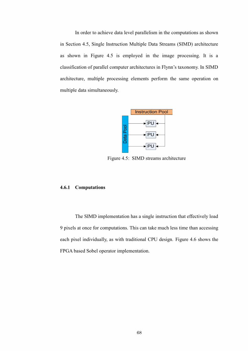
68
In order to achieve data level parallelism in the computations as shown
in Section 4.5, Single Instruction Multiple Data Streams (SIMD) architecture
as shown in Figure 4.5 is employed in the image processing. It is a
classification of parallel computer architectures in Flynn‟s taxonomy. In SIMD
architecture, multiple processing elements perform the same operation on
multiple data simultaneously.
Figure 4.5: SIMD streams architecture
4.6.1 Computations
The SIMD implementation has a single instruction that effectively load
9 pixels at once for computations. This can take much less time than accessing
each pixel individually, as with traditional CPU design. Figure 4.6 shows the
FPGA based Sobel operator implementation.
69
Figure 4.6: FPGA based Sobel operator implementation
In Figure 4.6, the Sobel operator implementation in X-direction is
shown; same implementation is applied in Y-direction. At each node, each
pixel is multiplied with a fixed coefficient. This was implemented by using the
multiplier-adder (ALTMULT_ADD) function that consists of 3 multipliers for
each line data. The data is shifted for processing as shown in Figure 4.6. Each
multiplier accepts a pair of inputs which are the pixel value and the fixed
coefficient, the product is then added to the products of all other pairs. For
computations of the gradient in Y-direction, different coefficients are used.
Figure 4.7 shows the Verilog code that initiates the multiplier-adder
computations of three line data with three ALTMULT_ADD blocks in X-
direction.
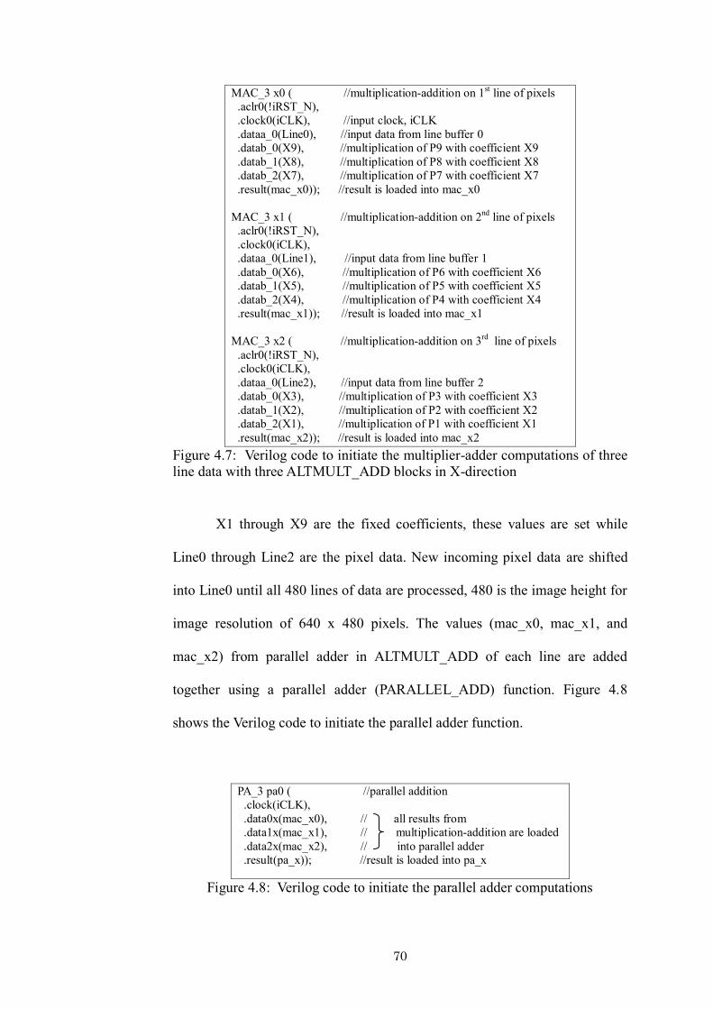
70
MAC_3 x0 ( //multiplication-addition on 1st line of pixels
.aclr0(!iRST_N),
.clock0(iCLK), //input clock, iCLK
.dataa_0(Line0), //input data from line buffer 0
.datab_0(X9), //multiplication of P9 with coefficient X9
.datab_1(X8), //multiplication of P8 with coefficient X8
.datab_2(X7), //multiplication of P7 with coefficient X7
.result(mac_x0)); //result is loaded into mac_x0
MAC_3 x1 ( //multiplication-addition on 2nd
line of pixels
.aclr0(!iRST_N),
.clock0(iCLK),
.dataa_0(Line1), //input data from line buffer 1
.datab_0(X6), //multiplication of P6 with coefficient X6
.datab_1(X5), //multiplication of P5 with coefficient X5
.datab_2(X4), //multiplication of P4 with coefficient X4
.result(mac_x1)); //result is loaded into mac_x1
MAC_3 x2 ( //multiplication-addition on 3rd
line of pixels
.aclr0(!iRST_N),
.clock0(iCLK),
.dataa_0(Line2), //input data from line buffer 2
.datab_0(X3), //multiplication of P3 with coefficient X3
.datab_1(X2), //multiplication of P2 with coefficient X2
.datab_2(X1), //multiplication of P1 with coefficient X1
.result(mac_x2)); //result is loaded into mac_x2
Figure 4.7: Verilog code to initiate the multiplier-adder computations of three line data with three ALTMULT_ADD blocks in X-direction
X1 through X9 are the fixed coefficients, these values are set while
Line0 through Line2 are the pixel data. New incoming pixel data are shifted
into Line0 until all 480 lines of data are processed, 480 is the image height for
image resolution of 640 x 480 pixels. The values (mac_x0, mac_x1, and
mac_x2) from parallel adder in ALTMULT_ADD of each line are added
together using a parallel adder (PARALLEL_ADD) function. Figure 4.8
shows the Verilog code to initiate the parallel adder function.
PA_3 pa0 ( //parallel addition
.clock(iCLK),
.data0x(mac_x0), // all results from
.data1x(mac_x1), // multiplication-addition are loaded
.data2x(mac_x2), // into parallel adder
.result(pa_x)); //result is loaded into pa_x
Figure 4.8: Verilog code to initiate the parallel adder computations

71
The results from parallel adders, pa_x and pa_y for both X and Y-
direction are then fed into square root (ALT_SQRT) function to find the
absolute magnitude of the gradient, G as explained in Section 4.5. Figure 4.9
shows the Verilog code to initiate the square root function. With the
implementation as discussed above, the system computes G value for one
pixel in just one clock cycle.
SQRT sqrt0 ( //square root function
.clk(iCLK),
.radical(pa_x * pa_x + pa_y * pa_y), //results from parallel adders are loaded
.q(abs_mag)); //absolute magnitude of the gradient, G
Figure 4.9: Verilog code to initiate the square root functions
The multipliers and adders of the ALTMULT_ADD are placed in
dedicated DSP block circuitry of the Cyclone II device. The pixel data width is
10-bit. However, the work covered in this thesis uses the 9 x 9-bit input
multiplier configuration in the DSP block instead of 18 x 18-bit input
multipliers to process the data. This is due to limited dedicated multiplier on
the device. As a solution, the least significant bits (LSB) of the pixel data are
truncated. There are multiple ALTMULT_ADD blocks occur in the design
thus all functions are distributed to available DSP blocks.
4.6.2 Line Buffer
Line buffer is needed to store the pixel data from SDRAM so that
Sobel edge detection calculations can be performed as in Figure 4.6. As
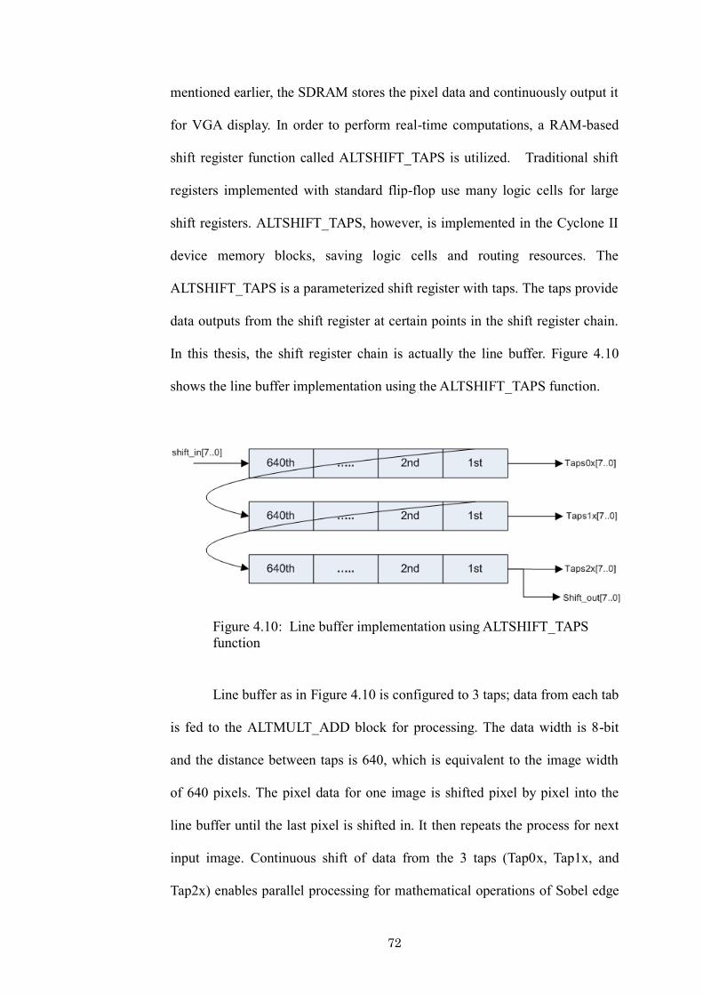
72
mentioned earlier, the SDRAM stores the pixel data and continuously output it
for VGA display. In order to perform real-time computations, a RAM-based
shift register function called ALTSHIFT_TAPS is utilized. Traditional shift
registers implemented with standard flip-flop use many logic cells for large
shift registers. ALTSHIFT_TAPS, however, is implemented in the Cyclone II
device memory blocks, saving logic cells and routing resources. The
ALTSHIFT_TAPS is a parameterized shift register with taps. The taps provide
data outputs from the shift register at certain points in the shift register chain.
In this thesis, the shift register chain is actually the line buffer. Figure 4.10
shows the line buffer implementation using the ALTSHIFT_TAPS function.
Figure 4.10: Line buffer implementation using ALTSHIFT_TAPS
function
Line buffer as in Figure 4.10 is configured to 3 taps; data from each tab
is fed to the ALTMULT_ADD block for processing. The data width is 8-bit
and the distance between taps is 640, which is equivalent to the image width
of 640 pixels. The pixel data for one image is shifted pixel by pixel into the
line buffer until the last pixel is shifted in. It then repeats the process for next
input image. Continuous shift of data from the 3 taps (Tap0x, Tap1x, and
Tap2x) enables parallel processing for mathematical operations of Sobel edge
73
detection.
4.6.3 Performance
The complete vision system which includes Sobel edge detection on
real-time input images as shown in Figure 4.3 was implemented on Altera
DE1 board. DE1 board includes a 16-pin D-SUB that can support standard
VGA resolution of 640 x 480 pixels, at 25 MHz. As such, the Sobel edge
detection was designed to operate at 25 MHz with image resolution of 640 x
480 pixels.
Threshold value for Sobel edge detection can be adjusted for different
operating conditions. Figure 4.11 shows the real-time images captured using
two different threshold values where the image on the right shows clearly
edges from that environment. However, it operates at only 9 frames per second
(fps) due to camera hardware limitations; TRDM_D5M is slow in capturing
real-time image especially under low light conditions. Anyway, Sermanet et al
(2009) had demonstrated a system that used 5-10 fps for near range obstacle
detection and 1 fps for far range obstacle detection.
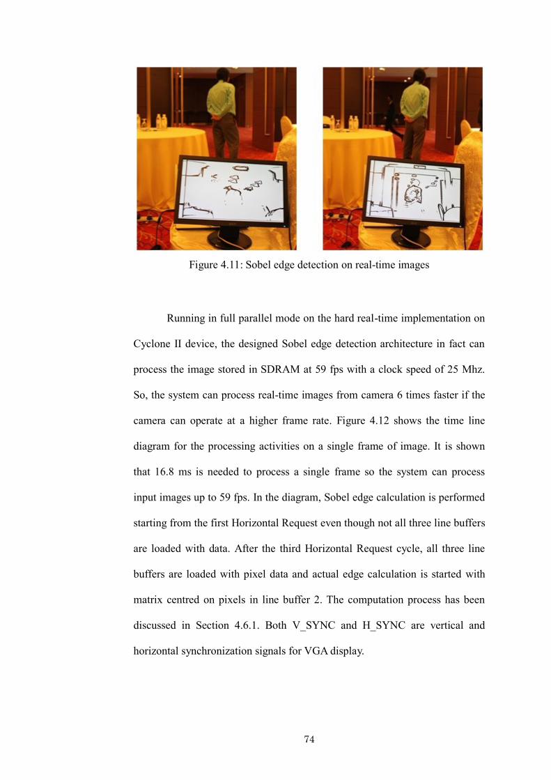
74
Figure 4.11: Sobel edge detection on real-time images
Running in full parallel mode on the hard real-time implementation on
Cyclone II device, the designed Sobel edge detection architecture in fact can
process the image stored in SDRAM at 59 fps with a clock speed of 25 Mhz.
So, the system can process real-time images from camera 6 times faster if the
camera can operate at a higher frame rate. Figure 4.12 shows the time line
diagram for the processing activities on a single frame of image. It is shown
that 16.8 ms is needed to process a single frame so the system can process
input images up to 59 fps. In the diagram, Sobel edge calculation is performed
starting from the first Horizontal Request even though not all three line buffers
are loaded with data. After the third Horizontal Request cycle, all three line
buffers are loaded with pixel data and actual edge calculation is started with
matrix centred on pixels in line buffer 2. The computation process has been
discussed in Section 4.6.1. Both V_SYNC and H_SYNC are vertical and
horizontal synchronization signals for VGA display.

75
1Line Buffer 1
Line Buffer 2
Line Buffer 3
2
1
3
2
1
4
3
2
640
639
638
1 2 3 4 480…..
…..
Horizontal
Request
Vertical
Request32us
16.8ms
Edge
Detection
Processing
H_SYNC
V_SYNC
Time(ms)
Activities
Edge
Detection
Processing
Edge
Detection
Processing
Edge
Detection
Processing
Edge
Detection
Processing
Figure 4.12: Time line diagram of processing activities on single frame of
image
In order to enable the high speed vehicle to move at 40 km/hr with on-
the-fly perception build up speed, the UTAR-CRCS needs to demonstrate its
capability to carry out the same algorithm as in high specification PC, but with
much higher speed. As an example, the image processing capability of UTAR-
CRCS was compared to a high specification Intel Core2 Duo 2.0 GHz
processor. The PC system consists of Windows Vista operating system and
with Matlab installed.
An image with resolution of 640 x 480 pixels was stored in the RAM
of the PC. The CPU time is recorded to observe the actual implementation of
the algorithm processing time. Simple Sobel edge detection is used as the
fundamental algorithm for the image processing task of the vehicle. Image was
loaded to memory before processing. This was same as UTAR-CRCS setup
used for comparisons where the Sobel edge detection module is set to process
the image stored in SDRAM instead of real-time image from camera.
76
Table 4.2: Comparisons of image processing time between UTAR-CRCS and
PC based processing unit
Number of Frames Processing Time (s) Frames per Second (fps)
UTAR-CRCS PC UTAR-CRCS PC
1 0.0176 0.1123 56.8 8.9
10 0.1790 1.3104 55.9 7.6
100 1.7845 13.4411 56.0 7.4
1000 17.9970 136.114 55.6 7.3
Table 4.2 lists the comparisons between the 2 different processing
environments. Both systems were set to process a fixed number of input
images and the processing time was recorded. The processing time for both
systems was derived from the average reading of a few run. It is clearly shown
that UTAR-CRCS can process input images at a much higher speed compared
to the high specification PC system. In UTAR-CRCS, the hard real-time
implementation shows that the Sobel edge computation can be carried out
within a defined timeframe for an input frame rate of about 56 fps. On the
other hand, the processing capability of high specification PC declines with an
increase in the number of input images. For real-time operations which might
process large amount of images, UTAR-CRCS is expected to outperform a
high specification PC based system. Another advantage is the number of gates
used in the process. The FPGA system utilize 2127 logic elements, only 11 %
of the total logic elements available on Cyclone II, while a normal PC
platform will consume high power and high number of logic elements
compared to the UTAR-CRCS. Thus, using such high power consumption and
large processing PC system will make agile autonomous agent impossible to
move in decimetre scale environment.
77
Stereo camera is widely used in the autonomous navigation to perceive
the environment. Teoh (2011) utilized a stereo camera set that can measure up
to 8 m of range at 27 x 2 fps. For a vehicle to run at higher speed, non-myopic
image processing task is essential to the success of the navigation objectives.
Thus, typical stereo cameras might need to extend its baselines up to 30 m of
the extended target and obstacle detection. Thus, it is necessary to process up
to 3 stereo pairs of images at 3 set of stereo cameras at any given time. Given
UTAR-CRCS can process up to 56 fps, the time to process 6 images (from
stereo) is 107 ms, so the total response time for processing input images from
a stereo set is as following:
Tresponse(stereo) = Tcamera-SDRAM + Tprocessing 4.4
Tresponse(stereo) = 110 ms + 107 ms = 217 ms 4.5
where Tcamera-SDRAM is time needed for the camera to grab a real-time image
and store it in on-board memory, and Tprocessing is time needed to process 6
images at 56 fps.
Imagine an ALV moving at a speed of 40 km/h which is 11.11 m/s, the
time to process real-time images from stereo, Tresponse(stereo) is only 217 ms. In
this case, the ALV have sufficient time to respond to the environment in real-
time manner. Note that the Tresponse(stereo) can be further reduced by using a
faster processing clock or higher performance camera module. Whereas for a
high specification PC to process the same task, it may take up to 7 times

78
longer than an FPGA based system, which may make it too late to make
navigation decision in less than a second in this particular specification. Thus,
a high specification PC system will need larger power consumption and higher
processing power for the same task that can be achieved by UTAR-CRCS
architecture.
4.7 Kalman Filtering for Tree Trunk Detection
In unstructured environment, the ability to extract useful features from
real-time images provides important guidance to successful autonomous
navigation. Teoh (2010) presented the use of U-disparity image and Sobel
edge detector to extract meaningful cues that can be used to detect tree trunks.
U-disparity image is based on disparity map obtained from the stereo camera.
Figure 4.13 shows a sample scene from the research with the detected tree
trunks in magenta.
Figure 4.13: Sample scene with tree trunks as obstacles and the detected tree
trunks in magenta
79
A NIOS II processor can be added to the UTAR-CRCS to implement
functions used to detect tree trunks as demonstrated in Figure 4.13. The NIOS
II processor only occupies a small amount of logic on the FPGA device. In
addition, the NIOS II fast processor core can use a memory management unit
(MMU) to run embedded Linux. The Nios II processor core meets both hard
and soft real-time requirements with the ability to use FPGA hardware to
accelerate a function. This thesis has demonstrated a full parallel Sobel edge
detector implementation on hard real-time platform. In the high-level
navigation system of UTAR-CRCS, a filter is needed in sensor fusion and data
fusion. The implementation of a Kalman filter will be described subsequently
using tree trunks detection as an example.
Given the detected tree trunks in the initial frame as in Figure 4.13, the
tree trunks can be tracked in subsequent frames by performing tree trunks
detection in each frame. This, however, will slow down the real-time
performance of tree trunks detection since it needs to search the entire image
of each frame. If a vehicle is moving in a fast manner, it might not be able to
avoid the tree trunk. As a solution, the searching algorithm can be done more
efficiently with the use of prediction and detection scheme; Kalman filtering
provides a mechanism to achieve this. The Kalman filter is an optimal linear
estimator based on iterative and recursive process (Drolet et al., 2000). It
recursively evaluates an optimal estimate of the state of a linear system.
Kalman filter process consists of two main steps; state update (prediction) step,
and measurement update (correction) step.
80
The state of a tree trunk at each frame can be characterized by its
position and the vehicle‟s velocity. Let (xt, yt) represent the position at time t,
and ),( t
y
t
x vv be the vehicle‟s velocity at time t in x and y direction respectively.
Therefore, the state vector Xt is represented as t
y
t
xttt vvyxX ,,, .
Measurement vector Zt is defined to represent the position of tree trunks at
time t. The state vector Xt and measurement vector Zt are related in the
following basic system model equations:
Xt = AXt-1 + ωt-1 4.6
Zt = H Xt + υt 4.7
where A is known as the state transition matrix, and H is the measurement
matrix that relates the state to the measurement Zt. The variable ω is the
process noise, and υ is the measurement noise with normal probability
distributions
p(ω) ~ N(0,Q) 4.8
p(υ) ~ N(0,R) 4.9
where Q is process noise covariance and R is measurement noise covariance.
81
Based on the system model equations above, a few more variables are
defined for subsequent discussion. Let Xt+1(prior) be the estimated state at time
t+1, it is often referred as prior state estimation. Besides, Xt+1 is referred to the
posterior state estimation. Given the prior estimate Xt+1(prior), tree trunks
detection is performed to detect tree trunks around Xt+1(prior) area. The search
area is therefore adaptively adjusted and the tree trunk can be detected quickly.
After that, the process is formalized by comparing the Xt+1(prior) with state
measurement, Zt+1, yielding the posterior state estimation Xt+1 as follow:
Xt+1 = Xt+1(prior) + Kt+1 (Zt+1 - H Xt+1(prior)) 4.10
where Kt+1 is the Kalman gain. Jose et al (2000) explained the process of
obtaining Kalman gain. After each time and measurement update pair, the
process is repeated with the previous posterior estimates used to predict the
new prior estimates. This recursive nature is one of the very appealing features
of Kalman filter.
4.8 Summary
The need for machine vision in autonomous navigation had led to rapid
research and development in real-time vision processing. For real-time
applications, the processing speed must be fast enough to meet the process
deadline. This chapter demonstrated a full parallel FPGA based Sobel edge
detection that can process real-time input images up to 9 fps and non real-time
82
images up to 56 fps. In comparison to PC based system on non real-time
image processing, the direct hardware implementation in this thesis shows a
great advantage in processing speed as it can accelerates the computations.
The implementation of Kalman filtering for tree trunk detection is also
introduced. A successful implementation of the filter will further enhance the
real-time performance in autonomous navigation.

83
CHAPTER 5
RESULTS AND DISCUSSIONS
5.1 Overview
UTAR-CRCS consists of multiple modules that were designed and
simulated using Quartus II design software and then implemented on Altera
DE1 board. The complete system is complicated so multiple simulations were
performed to ensure the functionalities and performance. This chapter will
present some simulations that were performed using Quartus II together with
the simulations results. The system outputs from DE1 board were measured
and compared with design expectations. Besides, some of the system
performances are described and compared to multiple-CPU control systems.
5.2 Simulations
In typical design flow, simulations must be run on the individual
functional block to check on the block‟s functionalities before system
integration. After the system integration to create the UTAR-CRCS,
simulations are then performed on the complete system to observe the system
behaviours. If a faulty custom functional block is not verified and it is
integrated into UTAR-CRCS, it is difficult to detect the fault from multiple
blocks in the later design stage, and system performance is not guaranteed. So,
simulations are useful to meet certain needs, including the following cases:

84
To verify the functionalities of a custom component before
implementing it on hardware
To verify the cycle-accurate performance of a system before
target hardware is available
5.2.1 Vector Waveform File
Vecfor Waveform File (VWF) describes the simulation input vectors
and simulation output vectors as graphical waveforms. Waveform Editor is
used to view and edit VWF. During simulation, the VWF is an input file only.
The Simulator requires a VWF to provide the input vectors that drive
simulation. In order for a VWF to be used in creating stimulus for the
Simulator, it must specify the following:
The input logic levels (vectors) that drive the input pins and
determine the internal logic levels throughout the design
The nodes to be observed, start and stop times for applying
vectors, intervals at which vectors are applied
The radix used to interpret logic levels

85
5.2.2 Custom Component Block Level Simulation
There are multiple blocks used to build the complete system. As a
demonstration, simulation that was performed on the FSM block in vehicle
control module as shown in Figure 3.15 is discussed in details. The FSM is a
control mechanism that ensures safety operations of the DC motors so it must
be verified before implementation. Table 5.1 lists the binary values of each
FSM state in the system.
Table 5.1: Binary value of FSM states
STATE STATE VALUE (BINARY)
Stop/Brake 000
Clear Brake 001
Forward 010
Reverse 011
Clear Throttle 100
Figure 5.1: Vehicle control module FSM simulation
Figure 5.1 shows the simulation of the FSM in vehicle control module.
The input vectors for this simulation are CLOCK, RESET, FORWARD,
86
REVERSE, BRAKE, RPM. All these input vectors were defined and set in
Waveform Editor of Quartus II before simulation. For the first rising clock
edge, there are no activities in the input signals thus FSM remains in
Stop/Brake (000) state. At the second rising clock edge, the control system
asserts FORWARD to logic „high‟ and FSM jumps to Clear Brake (001) state
to prepare the vehicle for acceleration. Finally in the third rising clock edge,
FORWARD signal is still logic „high‟ thus FSM makes a transition to Forward
(010) state and vehicle accelerates to forward direction.
This simulation shows that FSM behaviours meet design expectations.
It makes a smooth and correct transition between states. In case error is found
from simulation, input vectors are checked to detect any incorrect input that
causes unpredictable behaviour. If error is not arising from incorrect input
vectors, component coding needs to be evaluated. Since this simulation is
focused on the functional verification instead of timing behaviour, so the
timescale is set to unit of micro-second in order to reduce the simulation time.
A larger time interval and time unit will increase the simulation time
significantly. However, if the design requires accurate timing behaviours from
simulation, the actual time scale has to be set.
5.2.3 System Level Simulation
After the simulations on each component block, all blocks are
connected using on-chip system interconnects to establish communications
between blocks. The complete system is verified by simulation with steps

87
similar to Section 5.2.2. Figure 5.2 shows simulation which consists of inputs
to the vehicle control system and the outputs after processing through internal
logics of multiple blocks.
Figure 5.2: UTAR-CRCS system level simulation
Before the simulation is run, input vectors are designed and defined so
that it can test various functionalities of the system. At this stage, system
outputs are known based on the design specifications without running the
simulation. The expected outputs are used to verify the simulation result, as
indicated by the output signals in Figure 5.2. The outputs that are of utmost
importance in the system are control signals and data to configure the external
Digital-to-Analog Converter (DAC) chip which controls DC motors. These
signals are labeled with “DA” in front of the signal name in the simulation

88
result. All waveforms are studied carefully to ensure that it meets design
specifications. From simulation, it shows that system sends correct
configuration data to DAC chip through SPI communication.
5.3 UTAR-CRCS Performance
UTAR-CRCS is a multiple module system built on Cyclone II FPGA
device. Cyclone II is a low-end FPGA device which is known to have fewer
features and lower specifications compared to high-end FPGA device like
Stratix V. However, the low-end Cyclone II still contains most of the features
offered in high-end device. In terms of implementation, Cyclone II is limited
in the processing speed, number of I/O available, and dedicated multiplier for
signal processing.
The Cyclone II device on DE1 board used in this thesis supported 315
I/O pins which are more than sufficient in this implementation. However, only
a certain amount of I/O pins on Cyclone II device is bonded out to the DE1
board. Thus, UTAR-CRCS was built using two DE1 boards due to insufficient
I/O pins that are bonded out on a single DE1 board. Table 5.2 lists the resource
utilization on a single Cyclone II device for the whole system that includes the
vision system. The assumption made here is that a single Cyclone II device is
used for processing. The logic elements usage is only 32 % which means there
is still room for more functional blocks. Besides, the complete system utilized
95 % of the total I/O pins count on the device indicates that it can support the
complete system implementation. Most of the 9-bit dedicated multipliers were

89
used in digital signal processing for the sensors and vision camera.
Table 5.2: FPGA resources utilization for UTAR-CRCS
Resources Available Used Usage (%)
Logic Elements 18,752 5,956 32
Pins 315 299 95
Memory – RAM (kB) 234 70 30
Embedded Multiplier 9-bit 52 51 98
PLL 4 1 25
Simulations in the previous section show that FPGA based UTAR-
CRCS has met the design expectations. The following section will highlight
some performances of UTAR-CRCS compared to multiple CPUs system.
5.3.1 Communication
In order to perform parallel processing, a number of autonomous
vehicle control systems are formed of multiple CPUs. These systems
communicate with each other by external communication ports. On the other
hand, UTAR-CRCS contains multiple modules in a chip that communicate
with on-chip communication. Table 5.3 compares the maximum data rate of
multiple CPUs system with UTAR-CRCS. In this comparison, USB2.0 is
chosen for multiple CPUs system since it is commonly used as communication
between CPUs as discussed in Section 3.4.3.1. For UTAR-CRCS, the data
transfer rate for module shown in Figure 3.19 in Section 3.4.3.1 is used for this
comparison.

90
Table 5.3: Comparison of maximum data rate between multiple CPUs system
and UTAR-CRCS
System (Communication) Data Rate Clock Speed
Multiple CPUs
(USB 2.0) 480 Mbps 480 MHz
UTAR-CRCS
(On-Chip Communication) 475 Mbps
1 12.5 MHz
1 Calculation based on the parallel communication between high-level navigation
module and low-level vehicle control module as shown in Figure 3.19
Although different clocks are used in the system, this 12.5 MHz clock
achieves maximum data rate since it clocks the transfer of 38-bit data through
parallel communication between two modules. USB 2.0 in multiple CPUs
system can support data rate up to 480 Mbps with a clock of 480 MHz.
However, UTAR-CRCS has a maximum data rate of 475 Mbps with a clock
speed of merely 12.5 MHz. The data rate of 475 Mbps is deemed sufficient in
this implementation. On-chip communication allows data to be transmitted in
parallel mode instead of serial mode for off-chip communication. Besides, the
data rate is scalable by using different clock speed which means data rate can
be further increased by using a higher clock speed. In addition, system that
operates with lower clock frequency will consume lower power compared to
higher clock frequency (Mahesri & Vardhan, 2004). This is due to the fact that
dynamic power consumption is directly proportional to clock frequency as
shown in the following equation:
fCVP 2 5.1
where f is the clock frequency, C is the capacitance, and V is the operating
voltage.

91
5.3.2 Deterministic System Behaviour
Measurement of the system output signals is an important step after
implementation. The system performance can be analysed using various kinds
of measurements. In this thesis, all the outputs from systems were measured
using an oscilloscope. As HDL implements the functions directly on the
hardware logic, this hard-real time system assures continuity in system
behaviour and output signals.
Figure 5.3: Measured signals from DAC chips to DC motor controllers
Figure 5.3 shows the measured signals from DAC chip to DC motor
controller. Inputs to the real-time system are signals from the remote control.
When the remote control sends command to move forward, both DC motor
controllers receive the same input control voltage from the system in order to
move in forward direction. In order to make a right turn, DC motor controller
on the left wheel will receive higher control voltage which results in higher
speed than right wheel. Measurements on the system show accurate and
consistent output from the real-time system.
1.6 V
1.6 V 1.6 V
2.4 V
92
5.3.3 Compact System
This thesis describes work done to build an autonomous vehicle
control system that is compact which can be installed on a compact
autonomous vehicle. The literature review in Chapter 2 shows some
autonomous vehicle control systems that consist of multiple CPUs or a
combination of multiple CPUs with multiple processing devices such as
microcontrollers and digital signal processors. After reviewing some available
systems, this research focused on FPGA based platform where UTAR-CRCS
was built on two Altera DE 1 boards.
In this research, UTAR-CRCS does not claim itself to outperform
multiple CPUs system in every aspect. First, in term of computing power,
Cyclone II on DE1 board might not perform faster than some supercomputer
or high-end computing device but advance in FPGA technology enabled the
device to outperform CPU in certain applications (Asano et al., 2009). Second,
DE1 board doesn‟t consist of certain hardware resources or software that is
available on computer. However, some available hardware resources on a
computer might not be useful in building an autonomous vehicle control
system; it might be a waste of resources and lead to increase in power
consumption. In comparison, FPGA device consists of dedicated DSP blocks
for signal processing and logic gates that can be configured to work as a
microcontroller.

93
The UTAR-CRCS system studied in this research claims itself as
compact system by comparing to some available embedded real-time
operating system in the market in terms of size and weight. These real-time
operating system can be used to build the autonomous vehicle RCS. Table 5.4
lists the dimension, weight, and power consumption for DE1 board, Mobile
Real-Time Target Machine, and a Basic Real-Time Target Machine for
comparisons. Both Mobile Real-Time Target Machine and Basic Real-Time
Target Machine is real-time operating machine with embedded CPU and xPC
Target.
The DE1 board size is only about half the size of a Basic Real-Time
Target Machine. Besides, the weight of 0.28 kg is much lower than other real-
time machine listed in the table; it is only 14 % of the weight for a Basic Real-
Time Target Machine. The Mobile Real-Time Target Machine has much
greater dimension and weight compared to DE1. Both the weight and size
comparisons show that UTAR-CRCS is more compact. The DE1 board is
powered up by USB port of laptop in this research and only draws a maximum
power of 2.5 W according to the USB power rating specifications. This is
much lower than the power consumption of both the real-time machines.
Table 5.4: Comparisons between DE1 and Real-Time Target Machine
Processing Platform
(Embedded Board /
embedded operating system)
Dimension (cm)
(W x H x D) Weight (kg)
Power
Consumption
(W)
Altera DE1 15.00 x 3.00 x 15.00 0.28 2.50
Mobile Real-Time
Target Machine 43.10 x 13.20 x 48.00 15.00 300.00
Basic Real-Time
Target Machine 27.00 x 8.20 x 16.20 2.00 400.00

94
5.4 Summary
This chapter presents the simulations performed on the UTAR-CRCS
for both individual blocks and the final integrated system. In this system
development, simulations can verify functionalities of multiple blocks thus
system performance is guaranteed. Besides, system output signals are
measured to check on the performance after implementation on DE1 board.
During the measurements, accurate and continuity in output signals had been
observed. The low-end Cyclone II device used in this research doesn‟t have a
high computing performance if compared to high-end computer or
supercomputer. However, the comparisons made in this chapter highlighted
certain advantages of FPGA-based system over embedded real-time operating
system particularly in size, weight, and power consumption.

95
CHAPTER 6
CONCLUSION AND FUTURE WORK
This chapter contains a conclusion of the work presented as part of this
thesis and presents some starting points for future explorations.
6.1 Conclusion
Motivated by the need of a compact autonomous vehicle in confined
environment for search and rescue mission, a compact FPGA based RCS with
the name of UTAR-CRCS was developed. Its main goal is to realise the
parallelization across multiple modules using FPGA technology. In this control
system, FPGA device works as processing unit, microcontrollers, and digital
signal processors.
All modules were designed and integrated in Quartus II software using
custom built blocks and IP blocks. In the design stage, module specifications
were clearly defined by control flow and data flow. On-chip communication
was established for inter-modules data exchange and the parallel mode
communication allows high data transfer rate between modules. Off-chip
communications allow the control system to communicate with external
devices, which is needed for sensors configurations and data acquisition. Both
the simulations and measurements demonstrate that the control system has
achieved stability and continuity in generating accurate output signals. The

96
simulations that were performed on all blocks and system are important
verification on the functionalities before hardware implementation. Without
simulations, it is difficult to locate the errors by debugging directly on the
hardware.
Besides, this research also intends to enhance the real-time visual
guidance system through implementation using FPGA device. The Sobel edge
detection on real-time image was implemented in full parallel mode with the
dedicated DSP blocks to further accelerate the computation speed. This
system is capable of processing real-time input images up to 9 fps. For non-
real-time images, this direct hardware implementation has shown greater
processing speed when compared to a high specification PC based system. In
order to guarantee real-time performance, Kalman filtering can be introduced
to predict and detect the obstacles in unstructured environment.
UTAR-CRCS has shown some advantages against multiple CPUs
system and embedded operating systems. On-chip communication between
modules can be faster and more flexible than off-chip communication between
systems. Direct hardware logic implementation reduces system response time
thus real-time performance is guaranteed. More importantly, it is compact in
terms of size and weight. On the other hand, there are also limitations in this
system. This system performance is limited by the available I/O pins and
clocks on the DE1 board. Due to insufficient I/O pins, the vision system was
implemented on another DE1 board. Besides, the low-end Cyclone II device
comes with limited on-chip resources such as dedicated multiplier to facilitate
97
future expansion. However, the predictability of the system behaviours
achieved through this design concept is expected to be sufficient to provide the
necessary basis for the higher system design levels.
6.2 Future Work
This thesis has focused on the development of FPGA based real- time
control system for autonomous vehicle. In order for the control system to
operate in the field, more modules and sensors are needed. Besides, high-level
intelligent control system and teleoperation platform have to be developed.
An autonomous vehicle needs to sense the environment for
decision making during navigation. As such, it needs
information from Inertia Measurement Unit (IMU) to report on
vehicle velocity and orientation. It also needs LIDAR or
RADAR to complement vision system in perceiving the
environment. All these sensors are heavy computational load to
the control system so a high-end FPGA device can increase the
performance in sensory processing.
High-level of intelligence has to be implemented in the vehicle
navigation system. One of such solutions is Partially
Observable Markov Decision Process (POMDP) that helps to
solve navigation problems. With POMDP, the vehicle navigates
to the destination following the path that brings the maximum
98
rewards. Besides, POMDP can control the on board sensors
actively to yield optimum sensor performance and thus manage
the system power consumption.
Teleoperation system is needed to allow human-robot
cooperation. In real-time operations, the vehicle updates its
information with remote operator through wireless
communication. Real-time image, vehicle status such as battery
level is sent to the remote operator for further decision making.
The interaction mode can be manual, semi-autonomous or
autonomous depending on the task context and vehicle status.
The current UTAR-CRCS can be implemented on a single DE1
board by bonding out all 315 I/O pins to physical hardware. In
this case, it will integrate more tasks on the same board.

99
AUTHOR’S PUBLICATION
1. K.C Chan, C.S Tan, C.L Cheng, K.S Lee, C.L Kho, Y.S Fong and C.M
Teng. (2010), “Feasibility Study of FPGA Based Real-Time Controller
for Autonomous Vehicle Applications”, IEEE Conference on
Sustainable Utilization and Development in Engineering and
Technology (STUDENT), 20-21 November 2010, page(s): 1-6.

100
REFERENCES
Alberts, J., Edwards, D., Soule, T., Anderson, M., & O'Rouke, M. (2008).
Autonomous Navigation of an Unmanned Ground Vehicle in
Unstructured Forest Terrain. ECSIS Symposium on Learning and
Adaptive Behaviors for Robotic Systems, (pp. 103-108).
Anthony, F., & Steve, S. (2010). Developments and Chellenges for
Autonomous Unmanned Vehicles.
Asano, S., Maruyama, T., & Yamaguchi, Y. (2009). Performance Comparison
of FPGA, GPU and CPU in Image Processing. International
Conference on Field Programmable Logic and Applications, (pp. 126-
131). Prague.
Barbera, T., Albus, J., Messina, E., Schlenoff, C., & Horst, J. (2004). How
Task Analysis Can be Used to Derive and Organize the Knowledge of
the Control of Autonomous Vehicles. Robotics and Autonomous
Systems , 67-78.
Bellutta, P., Manduchi, R., Matthies, L., Owens, K., & Rankin, A. (2000).
Terrain Perception for DEMO III. Intelligent Vehicles Conference.
Colnaric, M., Verber, D., Gumzej, R., & Halang, W. A. (1998).
Implementation of Hard Real-Time Embedded Control Systems. Real-
Time Systems , 293-310.
Defense, U. D., Government, U., & Army, U. (2010). 2009-2034 Unmanned
Systems Integrated Roadmap . Progressive Management .
Drolet, L., Michaud, F., & Cote, J. (2000). Adaptable Sensor Fusion Using
Multiple Kalman Filters. IEEE/RSJ International Conference on
Intelligent Robots and Systems, 2000, (pp. 1434 - 1439).
Gomi, T. (2003). New AI and Service Robots. Industrial Robot , 123-138.
101
Guivant, J., Nebot, E., & Baiker, S. (2000). Autonomous Navigation and Map
Building Using Laser Range Sensors in Outdoor . Journal of Robotic
System , 565-583.
Kentaro, S., Nishikawa, T., Aoki, T., & Yamamoto, S. (2008). Evaluating
Power and Energy Consumption of FPGA-Based Custom Computing
Machines for Scientific Floating-Point Computation. International
Conference on ICECE Technology , (pp. 301-304). Taipei.
Kim, T., & Yuh, J. (2004). Development of a Real-Time Control Architecture
for a Semi-Autonomous Underwater Vehicle for Intervention Missions.
Control Engineering Practice 12 , 1521-1530.
Mahesri, A., & Vardhan, V. (2004). Power Consumption Breakdown on A
Modern Laptop.
Mahyuddin, M. N., Chan, Z. W., & Arshad, M. R. (2009). FPGA as an
Embedded System of a Mobile Robot with incorporated Neuro-Fuzzy
Algorithm for Obstacle Avoidance Mission. MASAUM Journal of
Basic and Applied Sciences , 361-367.
Manduchi, R., Castano, A., Talukder, A., & Matthies, L. (2005). Obstacle
Detection and Terrain Classification for Autonomous Off-Road
Navigation. Autonomous Robots , 81-102.
Meng, Y. (2006). An Agent-based Mobile Robot System Using Configurable
SoC Technique. IEEE International Conference on Robotics and
Automation, (pp. 3368-3373). Florida.
Murthy, S. N., Alvis, W., Shirodkar, R., Valavanis, K., & Moreno, W. (2008).
Methodology for Implementation of Unmanned Vehicle Control on
FPGA Using System Generator. 7th International Caribbean
Conference on Devices, Circuits and Systems, (pp. 1-6). Cancun.
102
Nebot, P., Torres-Sospedra, J., & Martinez, R. (2011). A New HLA-Based
Distributed Control Architecture for Agricultural Teams of Robots in
Hybrid Applications with Real and Simulated Devices or
Environments. Sensors , 4385-4400.
Neoh, H. S., & Hazanchuk, A. (2005). Altera Documentation. Retrieved
September 2011, from Altera Corporation Web Site:
www.altera.com/literature/cp/gspx/edge-detection.pdf
Park, M. W., Son, Y. J., & Kim, J. H. (2007). Design of the Real-Time Control
System for Controlling Unmanned Vehicle. International Conference
on Control, Automation and System, (pp. 1234-1237). Seoul, Korea.
Peng, J., & Peters, A. (2005). Extraction of Salient Features for Mobile Robot
Navigation via Teleoperation. American Control Conference, (pp.
4903-4908).
Sermanet, P., Hadsell, R., Scoffier, M., Grimes, M., Ben, J., Erkan, A., et al.
(2009). A Multi-Range Architecture for Collision-Free Off-Road Robot
Navigation. Journal of Field Robotics , 58-87.
Seunghun, J., Junguk, C., Xuan Dai, P., Kyoung Mu, L., Sung Kee, P.,
Munsang, K., et al. (2010). FPGA Design and Implementation of A
Real-Time Stereo Vision System. IEEE Transactions on Circuits and
Systems for Video Technology , 15-26.
Seward, D., Pace, C., & Agate, R. (2006). Safe and Effective Navigation of
Autonomous Robots in Hazardous Environments . Autonomous
Robots , 223-242.
Stentz, A. (1994). Optimal and Efficient Path Planning for Partially-Known
Environments. IEEE International Conference on Robotics and
Automation, (pp. 3310-3317).

103
Tee, Y. H., & Tan, Y. C. (2010). A Compact Design of Zero-Radius Steering
Autonomous Amphibious Vehicle with Direct Differential Directional
Drive - UTAR AAV. 2010 IEEE Conference on Robotics Automation
and Mechatronics (RAM), (pp. 176-181). Singapore.
Teoh, C. W. (2011). Near-Range Water Body Detection and Obstacle
Detection in Rainforest Terrain/ Tropical Terrain. M.Eng. Thesis,
Universiti Tunku Abdul Rahman, Malaysia .
Wade, S. F., & James, K. A. (2007). Reconfigurable On-Board Vision
Processing for Small Autonomous Vehicles. EURASIP Journal on
Embedded Systems .
Widyotriatmo, A., Hong, B., & Hong, K. S. (2009). Predictive Navigation of
an Autonomous Vehicle with Nonholomonic and Minimum Turning
Radius Constraints. Mechanical Science and Technology .
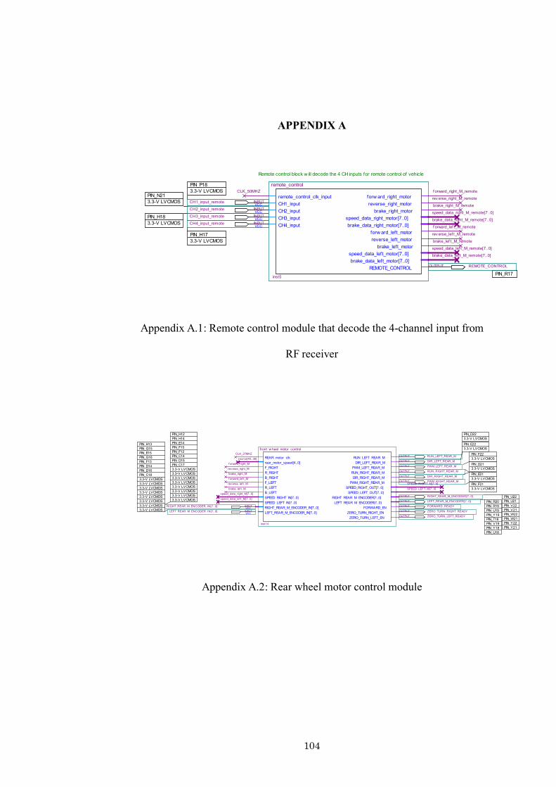
104
APPENDIX A
Appendix A.1: Remote control module that decode the 4-channel input from
RF receiver
Appendix A.2: Rear wheel motor control module
PIN_H18
3.3-V LVCMOSVCC
CH3_input_remote INPUT
PIN_P18
3.3-V LVCMOS
VCCCH1_input_remote INPUT
PIN_N21
3.3-V LVCMOS
VCCCH2_input_remote INPUT
PIN_H17
3.3-V LVCMOS
VCCCH4_input_remote INPUT
PIN_R17
REMOTE_CONTROLOUTPUT
remote_control_clk_input
CH1_input
CH2_input
CH3_input
CH4_input
forw ard_right_motor
reverse_right_motor
brake_right_motor
speed_data_right_motor[7..0]
brake_data_right_motor[7..0]
forw ard_left_motor
reverse_left_motor
brake_left_motor
speed_data_left_motor[7..0]
brake_data_left_motor[7..0]
REMOTE_CONTROL
remote_control
inst5
f orward_right_M_remote
rev erse_right_M_remote
brake_right_M_remote
speed_data_right_M_remote[7..0]
brake_data_right_M_remote[7..0]
f orward_lef t_M_remote
rev erse_lef t_M_remote
brake_lef t_M_remote
speed_data_lef t_M_remote[7..0]
brake_data_lef t_M_remote[7..0]
CLK_50MHZ
Remote control block w ill decode the 4 CH inputs for remote control of vehicle
PIN_H12
PIN_H14
PIN_E14
PIN_F15
PIN_F12
PIN_C14
PIN_D15
PIN_C17
3.3-V LVCMOS
3.3-V LVCMOS
3.3-V LVCMOS
3.3-V LVCMOS
3.3-V LVCMOS
3.3-V LVCMOS
3.3-V LVCMOS
3.3-V LVCMOS
VCCRIGHT_REAR_M_ENCODER_IN[7..0] INPUT
PIN_H13
PIN_G15
PIN_E15
PIN_G16
PIN_F13
PIN_D14
PIN_D16
PIN_C18
3.3-V LVCMOS
3.3-V LVCMOS
3.3-V LVCMOS
3.3-V LVCMOS
3.3-V LVCMOS
3.3-V LVCMOS
3.3-V LVCMOS
3.3-V LVCMOSVCC
LEFT_REAR_M_ENCODER_IN[7..0] INPUT
PIN_D22
3.3-V LVCMOS
RUN_LEFT_REAR_MOUTPUT
PIN_E22
3.3-V LVCMOS
DIR_LEFT_REAR_MOUTPUT
PIN_F22
3.3-V LVCMOS
PWM_LEFT_REAR_MOUTPUTPIN_D21
3.3-V LVCMOSRUN_RIGHT_REAR_MOUTPUT
PIN_E21
3.3-V LVCMOSDIR_RIGHT_REAR_MOUTPUT
PIN_F21
3.3-V LVCMOS
PWM_RIGHT_REAR_MOUTPUT
PIN_R20
PIN_R19
PIN_U19
PIN_Y19
PIN_T18
PIN_V19
PIN_Y18
PIN_U18
LEFT_REAR_M_ENCODER[7..0]OUTPUT
PIN_U22
PIN_U21
PIN_V22
PIN_V21
PIN_W22
PIN_W21
PIN_Y22
PIN_Y21
RIGHT_REAR_M_ENCODER[7..0]OUTPUT
ZERO_TURN_RIGHT_READYOUTPUT
ZERO_TURN_LEFT_READYOUTPUT
FORWARD_READYOUTPUT
REAR_motor_clk
rear_motor_speed[4..0]
F_RIGHT
R_RIGHT
B_RIGHT
F_LEFT
R_LEFT
B_LEFT
SPEED_RIGHT_IN[7..0]
SPEED_LEFT_IN[7..0]
RIGHT_REAR_M_ENCODER_IN[7..0]
LEFT_REAR_M_ENCODER_IN[7..0]
RUN_LEFT_REAR_M
DIR_LEFT_REAR_M
PWM_LEFT_REAR_M
RUN_RIGHT_REAR_M
DIR_RIGHT_REAR_M
PWM_RIGHT_REAR_M
SPEED_RIGHT_OUT[7..0]
SPEED_LEFT_OUT[7..0]
RIGHT_REAR_M_ENCODER[7..0]
LEFT_REAR_M_ENCODER[7..0]
FORWARD_EN
ZERO_TURN_RIGHT_EN
ZERO_TURN_LEFT_EN
front_w heel_motor_control
inst14
SPEED_RIGHT_M[7..0]
SPEED_LEFT_M[7..0]
CLK_27MHZ
source[40..36]
f orward_right_M
rev erse_right_M
brake_right_M
f orward_lef t_M
rev erse_lef t_M
brake_lef t_M
speed_data_right_M[7..0]
speed_data_lef t_M[7..0]
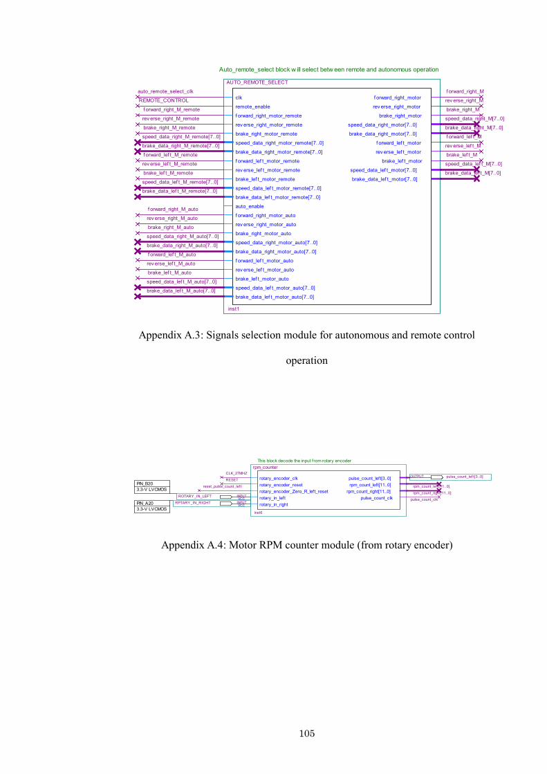
105
Appendix A.3: Signals selection module for autonomous and remote control
operation
Appendix A.4: Motor RPM counter module (from rotary encoder)
clk
remote_enable
f orward_right_motor_remote
rev erse_right_motor_remote
brake_right_motor_remote
speed_data_right_motor_remote[7..0]
brake_data_right_motor_remote[7..0]
f orward_lef t_motor_remote
rev erse_lef t_motor_remote
brake_lef t_motor_remote
speed_data_lef t_motor_remote[7..0]
brake_data_lef t_motor_remote[7..0]
auto_enable
f orward_right_motor_auto
rev erse_right_motor_auto
brake_right_motor_auto
speed_data_right_motor_auto[7..0]
brake_data_right_motor_auto[7..0]
f orward_lef t_motor_auto
rev erse_lef t_motor_auto
brake_lef t_motor_auto
speed_data_lef t_motor_auto[7..0]
brake_data_lef t_motor_auto[7..0]
f orward_right_motor
rev erse_right_motor
brake_right_motor
speed_data_right_motor[7..0]
brake_data_right_motor[7..0]
f orward_lef t_motor
rev erse_lef t_motor
brake_lef t_motor
speed_data_lef t_motor[7..0]
brake_data_lef t_motor[7..0]
AUTO_REMOTE_SELECT
inst1
rev erse_right_M
brake_right_M
speed_data_right_M[7..0]
brake_data_right_M[7..0]
f orward_lef t_M
rev erse_lef t_M
brake_lef t_M
speed_data_lef t_M[7..0]
brake_data_lef t_M[7..0]
REMOTE_CONTROL
f orward_right_M_remote
rev erse_right_M_remote
brake_right_M_remote
speed_data_right_M_remote[7..0]
brake_data_right_M_remote[7..0]
f orward_lef t_M_remote
rev erse_lef t_M_remote
brake_lef t_M_remote
speed_data_lef t_M_remote[7..0]
brake_data_lef t_M_remote[7..0]
f orward_right_Mauto_remote_select_clk
f orward_right_M_auto
rev erse_right_M_auto
brake_right_M_auto
brake_data_right_M_auto[7..0]
f orward_lef t_M_auto
rev erse_lef t_M_auto
brake_lef t_M_auto
brake_data_lef t_M_auto[7..0]
speed_data_right_M_auto[7..0]
speed_data_lef t_M_auto[7..0]
Auto_remote_select block w ill select betw een remote and autonomous operation
PIN_B20
3.3-V LVCMOS
VCCROTARY_IN_LEFT INPUT
PIN_A20
3.3-V LVCMOSVCC
RPTARY_IN_RIGHT INPUT
pulse_count_lef t[3..0]OUTPUTrotary_encoder_clk
rotary_encoder_reset
rotary_encoder_Zero_R_left_reset
rotary_in_left
rotary_in_right
pulse_count_left[3..0]
rpm_count_left[11..0]
rpm_count_right[11..0]
pulse_count_clk
rpm_counter
inst6
rpm_count_lef t[11..0]
rpm_count_right[11..0]
CLK_27MHZ
RESET
pulse_count_clk
reset_pulse_count_lef t
This block decode the input from rotary encoder
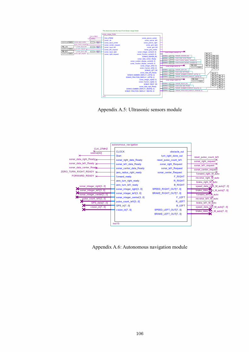
106
Appendix A.5: Ultrasonic sensors module
Appendix A.6: Autonomous navigation module
PIN_J18
3.3-V LVCMOSVCC
sonar_input_lef t INPUT
PIN_K21
3.3-V LVCMOSVCC
sonar_input_right INPUT
3.3-V LVCMOSVCC
sonar_input_center INPUT
PIN_F4
PIN_D5
PIN_D6
PIN_J4
PIN_L8
PIN_F3
PIN_D4
SONAR_NUMBER_DISPLAY_LEFT[6..0]OUTPUT
PIN_G5
PIN_G6
PIN_C2
PIN_C1
PIN_E3
PIN_E4
PIN_D3
SONAR_FRACTION_DISPLAY_LEFT[6..0]OUTPUT
PIN_E1
PIN_H6
PIN_H5
PIN_H4
PIN_G3
PIN_D2
PIN_D1
SONAR_NUMBER_DISPLAY_RIGHT[6..0]OUTPUT
PIN_J2
PIN_J1
PIN_H2
PIN_H1
PIN_F2
PIN_F1
PIN_E2
SONAR_FRACTION_DISPLAY_RIGHT[6..0]OUTPUT
sonar_number_display _center[6..0]OUTPUT
sonar_f raction_display _center[6..0]OUTPUT
PIN_K20
3.3-V LVCMOS
SONAR_LEFT_RXOUTPUT
sonar_data_lef t_ReadyOUTPUT
SONAR_CENTER_RXOUTPUT
sonar_data_center_ReadyOUTPUT
PIN_K22
3.3-V LVCMOS
SONAR_RIGHT_RXOUTPUT
sonar_data_right_ReadyOUTPUT
CLK_27MHZ
sonar_clk
sonar_input_center
sonar_center_request
sonar_input_left
sonar_left_request
sonar_input_right
sonar_right_request
sonar_pow er_center
sonar_pow er_left
sonar_pow er_right
sonar_gnd_right
sonar_gnd_left
sonar_gnd_center
sonar_integer_center[3..0]
sonar_fraction_center[4..0]
SONAR_CENTER_RX
sonar_data_center_Ready
sonar_number_display_center[6..0]
sonar_fraction_display_center[6..0]
sonar_integer_left[3..0]
sonar_fraction_left[4..0]
SONAR_LEFT_RX
sonar_data_left_Ready
SONAR_NUMBER_DISPLAY_LEFT[6..0]
SONAR_FRACTION_DISPLAY_LEFT[6..0]
sonar_integer_right[3..0]
sonar_fraction_right[4..0]
SONAR_RIGHT_RX
sonar_data_right_Ready
SONAR_NUMBER_DISPLAY_RIGHT[6..0]
SONAR_FRACTION_DISPLAY_RIGHT[6..0]
sonar_range_finder
inst2
This block decode the input from Sonar range f inder
CLK_27MHZ
CLK_50MHZ
sonar_lef t_request
sonar_right_request
sonar_integer_right[3..0]
sonar_integer_lef t[3..0]
sonar_integer_center[3..0]
sonar_center_request
CLOCK
Start
sonar_right_data_Ready
sonar_lef t_data_Ready
sonar_center_data_Ready
zero_radius_right_ready
f orward_ready
zero_turn_right_ready
zero_turn_lef t_ready
sonar_integer_right[3..0]
sonar_integer_lef t[3..0]
sonar_integer_center[3..0]
pulse_count_lef t[3..0]
GPS_in[7..0]
v ision_in[7..0]
obstacle_out
turn_right_done_out
reset_pulse_count_lef t
sonar_right_Request
sonar_lef t_Request
sonar_center_Request
F_RIGHT
R_RIGHT
B_RIGHT
SPEED_RIGHT_OUT[7..0]
BRAKE_RIGHT_OUT[7..0]
F_LEFT
R_LEFT
B_LEFT
SPEED_LEFT_OUT[7..0]
BRAKE_LEFT_OUT[7..0]
autonomous_nav igation
inst15
f orward_right_M_auto
rev erse_right_M_auto
brake_right_M_auto
speed_data_right_M_auto[7..0]
brake_data_right_M_auto[7..0]
f orward_lef t_M_auto
rev erse_lef t_M_auto
brake_lef t_M_auto
speed_data_lef t_M_auto[7..0]
brake_data_lef t_M_auto[7..0]
reset_pulse_count_lef t
sonar_right_request
sonar_lef t_request
sonar_center_request
source[42]
sonar_data_lef t_Ready
sonar_data_right_Ready
sonar_data_center_Ready
ZERO_TURN_RIGHT_READY
FORWARD_READY
pulse_count_lef t[3..0]
sonar_integer_right[3..0]
sonar_integer_lef t[3..0]
sonar_integer_center[3..0]
v ision_in[7..0]
GPS_data[7..0]
CLK_27MHZ

107
Appendix A.7: GPS receiver module
clk
RxD
RxD_data_ready
RxD_data[7..0]
RxD_endof packet
RxD_idle
GPS_Module
inst16
ClkFrequency 27000000 Signed Integer
Baud 4800 Signed Integer
Baud8 Signed Integer
Baud8GeneratorAccWidth 8 Signed Integer
Parameter Value Type
VCCGPS_RxD INPUT
CLK_27MHZ
GPS_data[7..0]
GPS_RxD_data_ready
GPS_RxD_endof packet
GPS_RxD_idle
PIN_F14
1.8 V

108
APPENDIX B
--remote control CH1 input processing
LIBRARY ieee;
USE ieee.std_logic_1164.all;
USE ieee.std_logic_unsigned.all;
USE ieee.std_logic_arith.all;
entity remote_control_decode_CH1 is
port( CH1_count: in std_logic_vector (15 downto 0); --number
from signal_counter, it counts the pulse width
enable : in std_logic; --it reads CH1_counter_aclr to make sure
that counter has done the count for one pulse
right_dir, left_dir : out std_logic;
data : out std_logic_vector (15 downto 0);
LED_test : out std_logic_vector (2 downto 0)); END
remote_control_decode_CH1;
architecture decode of remote_control_decode_CH1 is
signal LED_TEMP : STD_LOGIC_VECTOR(2 DOWNTO 0);
--store data before assign to output
signal data_temp : STD_LOGIC_VECTOR(15 DOWNTO 0);
--store data before assign to output
signal CH1_count_temp : STD_LOGIC_VECTOR(15 DOWNTO 0);
--assign input CH1_count to it for process
signal right_dir_temp, left_dir_temp : std_logic;
begin
process (enable)
begin
if (enable = '1') then
CH1_count_temp <= CH1_count;
end if;
end process;
process (CH1_count_temp)
begin
-- CH1_count < 18125
if (CH1_count_temp < "0100011011001101")then
data_temp <= ("0100011011001101" - CH1_count_temp);
LED_TEMP <= "100";
right_dir_temp <= '0';
left_dir_temp <= '1';
-- CH1_count > 19375
elsif (CH1_count_temp > "0100101110101111")then
data_temp <= (CH1_count_temp - "0100101110101111");
LED_TEMP <= "001";

109
right_dir_temp <= '1';
left_dir_temp <= '0';
else
data_temp <= "0000000000000000";
LED_TEMP <= "010";
right_dir_temp <= '0';
left_dir_temp <= '0';
end if;
end process;
LED_test <= LED_TEMP;
data <= data_temp;
right_dir <= right_dir_temp;
left_dir <= left_dir_temp;
end decode;
--remote control CH2 input processing
LIBRARY ieee;
USE ieee.std_logic_1164.all;
USE ieee.std_logic_unsigned.all;
USE ieee.std_logic_arith.all;
entity remote_control_decode_CH2 is
port( CH2_count: in std_logic_vector (15 downto 0); --number from
signal_counter, it counts the pulse width
enable : in std_logic;
--it reads CH1_counter_aclr to make sure that counter has done the
count for one pulse
brake : out std_logic;
data : out std_logic_vector (15 downto 0);
LED_test : out std_logic); --for testing purposes
END remote_control_decode_CH2;
architecture decode of remote_control_decode_CH2 is
signal LED_TEMP : STD_LOGIC;
--store data before assign to output
signal data_temp : STD_LOGIC_VECTOR(15 DOWNTO 0);
--store data before assign to output
signal CH2_count_temp : STD_LOGIC_VECTOR(15 DOWNTO 0);
--assign input CH1_count to it for process
signal brake_temp : std_logic;
begin
process (enable)
begin
if (enable = '1') then
CH2_count_temp <= CH2_count;
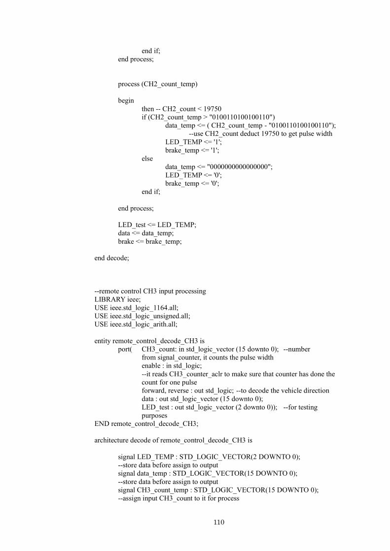
110
end if;
end process;
process (CH2_count_temp)
begin
then -- CH2_count < 19750
if (CH2_count_temp > "0100110100100110")
data_temp <= ( CH2_count_temp - "0100110100100110");
--use CH2_count deduct 19750 to get pulse width
LED_TEMP <= '1';
brake_temp <= '1';
else
data_temp <= "0000000000000000";
LED_TEMP <= '0';
brake_temp <= '0';
end if;
end process;
LED_test <= LED_TEMP;
data <= data_temp;
brake <= brake_temp;
end decode;
--remote control CH3 input processing
LIBRARY ieee;
USE ieee.std_logic_1164.all;
USE ieee.std_logic_unsigned.all;
USE ieee.std_logic_arith.all;
entity remote_control_decode_CH3 is
port( CH3_count: in std_logic_vector (15 downto 0); --number
from signal_counter, it counts the pulse width
enable : in std_logic;
--it reads CH3_counter_aclr to make sure that counter has done the
count for one pulse
forward, reverse : out std_logic; --to decode the vehicle direction
data : out std_logic_vector (15 downto 0);
LED_test : out std_logic_vector (2 downto 0)); --for testing
purposes
END remote_control_decode_CH3;
architecture decode of remote_control_decode_CH3 is
signal LED_TEMP : STD_LOGIC_VECTOR(2 DOWNTO 0);
--store data before assign to output
signal data_temp : STD_LOGIC_VECTOR(15 DOWNTO 0);
--store data before assign to output
signal CH3_count_temp : STD_LOGIC_VECTOR(15 DOWNTO 0);
--assign input CH3_count to it for process

111
signal forward_temp, reverse_temp : STD_LOGIC;
begin
process (enable)
begin
if (enable = '1') then
CH3_count_temp <= CH3_count;
end if;
end process;
process (CH3_count_temp)
begin
-- CH3_count < 17500
if (CH3_count_temp < "0100010001011100")then
data_temp <= ("0100010001011100" - CH3_count_temp);
LED_TEMP <= "100";
forward_temp <= '0';
reverse_temp <= '1';
-- CH3_count > 18750
elsif (CH3_count_temp > "0100100100111110")then
data_temp <= (CH3_count_temp - "0100100100111110");
LED_TEMP <= "001";
forward_temp <= '1';
reverse_temp <= '0';
else
data_temp <= "0000000000000000";
LED_TEMP <= "010";
forward_temp <= '0';
reverse_temp <= '0';
end if;
end process;
LED_test <= LED_TEMP;
data <= data_temp;
forward <= forward_temp;
reverse <= reverse_temp;
end decode;
--remote control CH4 input processing
LIBRARY ieee;
USE ieee.std_logic_1164.all;
USE ieee.std_logic_unsigned.all;
USE ieee.std_logic_arith.all;
entity remote_control_decode_CH4 is
port( CH4_count: in std_logic_vector (15 downto 0); --number
from signal_counter, it counts the pulse width

112
enable : in std_logic; --it reads CH4_counter_aclr to make sure that
counter has done the count for one pulse
Z_radius_right, Z_radius_left : out std_logic; --to decode the vehicle
zero radius turn direction
data : out std_logic_vector (15 downto 0);
LED_test : out std_logic_vector (2 downto 0)); --for testing
purposes
END remote_control_decode_CH4;
architecture decode of remote_control_decode_CH4 is
signal LED_TEMP : STD_LOGIC_VECTOR(2 DOWNTO 0);
--store data before assign to output
signal data_temp : STD_LOGIC_VECTOR(15 DOWNTO 0);
--store data before assign to output
signal CH4_count_temp : STD_LOGIC_VECTOR(15 DOWNTO 0);
--assign input CH3_count to it for process
signal Z_radius_right_temp, Z_radius_left_temp : STD_LOGIC;
begin
process (enable)
begin
if (enable = '1') then
CH4_count_temp <= CH4_count;
end if;
end process;
process (CH4_count_temp)
begin
-- CH4_count < 17500
if (CH4_count_temp < "0100010001011100")then
data_temp <= ("0100010001011100" - CH4_count_temp);
LED_TEMP <= "100";
Z_radius_right_temp <= '1';
Z_radius_left_temp <= '0';
-- CH4_count > 18875
elsif (CH4_count_temp > "0100100110111011")then
data_temp <= (CH4_count_temp - "0100100110111011");
LED_TEMP <= "001";
Z_radius_right_temp <= '0';
Z_radius_left_temp <= '1';
else
data_temp <= "0000000000000000";
LED_TEMP <= "010";
Z_radius_right_temp <= '0';
Z_radius_left_temp <= '0';
end if;
end process;
LED_test <= LED_TEMP;
data <= data_temp;

113
Z_radius_right <= Z_radius_right_temp;
Z_radius_left <= Z_radius_left_temp;
end decode;
--remote control processing
LIBRARY ieee;
USE ieee.std_logic_1164.all;
USE ieee.std_logic_unsigned.all;
USE ieee.std_logic_arith.all;
entity remote_control_processing is
port( clk : in std_logic;
forward, reverse : in std_logic;
speed_data_in : in std_logic_vector (7 downto 0);
right_dir, left_dir : in std_logic;
direction_data_in : in std_logic_vector (7 downto 0);
brake : in std_logic;
brake_data_in : in std_logic_vector (7 downto 0);
zero_R_right : in std_logic;
zero_R_left : in std_logic;
Z_radius_speed_in : in std_logic_vector (7 downto 0);
forward_right_motor : out std_logic;
reverse_right_motor : out std_logic;
brake_right_motor : out std_logic;
speed_data_right_motor : out std_logic_vector (7 downto 0);
brake_data_right_motor : out std_logic_vector (7 downto 0);
forward_left_motor : out std_logic;
reverse_left_motor : out std_logic;
brake_left_motor : out std_logic;
speed_data_left_motor : out std_logic_vector (7 downto 0);
brake_data_left_motor : out std_logic_vector (7 downto 0));
END remote_control_processing;
architecture processing of remote_control_processing is
--store input data
signal speed_data_in_temp : std_logic_vector (7 downto 0);
signal direction_data_in_temp : std_logic_vector (7 downto 0);
signal brake_data_in_temp : std_logic_vector (7 downto 0);
signal Z_radius_speed_in_temp : std_logic_vector (7 downto 0);
--store data before assign to output, act as buffer
signal forward_right_motor_temp : std_logic;
signal reverse_right_motor_temp : std_logic;
signal brake_right_motor_temp : std_logic;
signal speed_data_right_motor_temp : std_logic_vector (7 downto 0);
signal brake_data_right_motor_temp : std_logic_vector (7 downto 0);
signal forward_left_motor_temp : std_logic;
signal reverse_left_motor_temp : std_logic;
signal brake_left_motor_temp : std_logic;
signal speed_data_left_motor_temp : std_logic_vector (7 downto 0);
signal brake_data_left_motor_temp : std_logic_vector (7 downto 0);

114
begin
speed_data_in_temp <= speed_data_in;
direction_data_in_temp <= direction_data_in;
brake_data_in_temp <= brake_data_in;
Z_radius_speed_in_temp <= Z_radius_speed_in;
process (clk)
begin
if (clk'event and clk='1') then
if (brake='1')
then --brake, highest priority
forward_right_motor_temp <= '0';
reverse_right_motor_temp <= '0';
brake_right_motor_temp <= '1';
speed_data_right_motor_temp <= "00000000";
brake_data_right_motor_temp <= brake_data_in_temp;
forward_left_motor_temp <= '0';
reverse_left_motor_temp <= '0';
brake_left_motor_temp <= '1';
speed_data_left_motor_temp <= "00000000";
brake_data_left_motor_temp <= brake_data_in_temp;
elsif (forward='1' and reverse='0' and right_dir='0' and left_dir='0' )
then --move forward, both wheel same speed
forward_right_motor_temp <= '1';
reverse_right_motor_temp <= '0';
brake_right_motor_temp <= '0';
speed_data_right_motor_temp <= speed_data_in_temp;
brake_data_right_motor_temp <= "00000000";
forward_left_motor_temp <= '1';
reverse_left_motor_temp <= '0';
brake_left_motor_temp <= '0';
speed_data_left_motor_temp <= speed_data_in_temp;
brake_data_left_motor_temp <= "00000000";
elsif (forward='0' and reverse='1' and right_dir='0' and left_dir='0' )
then --move reverse, both wheel same speed
forward_right_motor_temp <= '0';
reverse_right_motor_temp <= '1';
brake_right_motor_temp <= '0';
speed_data_right_motor_temp <= speed_data_in_temp;
brake_data_right_motor_temp <= "00000000";
forward_left_motor_temp <= '0';
reverse_left_motor_temp <= '1';
brake_left_motor_temp <= '0';
speed_data_left_motor_temp <= speed_data_in_temp;
brake_data_left_motor_temp <= "00000000";
elsif (forward='1' and reverse='0' and right_dir='1' and left_dir='0' )
then --turn right, reduce right wheel speed
forward_right_motor_temp <= '1';
reverse_right_motor_temp <= '0';
brake_right_motor_temp <= '0';
speed_data_right_motor_temp <= (speed_data_in_temp -
direction_data_in_temp);

115
brake_data_right_motor_temp <= "00000000";
forward_left_motor_temp <= '1';
reverse_left_motor_temp <= '0';
brake_left_motor_temp <= '0';
speed_data_left_motor_temp <= speed_data_in_temp;
brake_data_left_motor_temp <= "00000000";
elsif (forward='1' and reverse='0' and right_dir='0' and left_dir='1' )
then --turn left, reduce left wheel speed
forward_right_motor_temp <= '1';
reverse_right_motor_temp <= '0';
brake_right_motor_temp <= '0';
speed_data_right_motor_temp <= speed_data_in_temp;
brake_data_right_motor_temp <= "00000000";
forward_left_motor_temp <= '1';
reverse_left_motor_temp <= '0';
brake_left_motor_temp <= '0';
speed_data_left_motor_temp <= (speed_data_in_temp -
direction_data_in_temp);
brake_data_left_motor_temp <= "00000000";
elsif (forward='0' and reverse='1' and right_dir='1' and left_dir='0' )
then --reverse right, reduce right wheel speed
forward_right_motor_temp <= '0';
reverse_right_motor_temp <= '1';
brake_right_motor_temp <= '0';
speed_data_right_motor_temp <= (speed_data_in_temp -
direction_data_in_temp);
brake_data_right_motor_temp <= "00000000";
forward_left_motor_temp <= '0';
reverse_left_motor_temp <= '1';
brake_left_motor_temp <= '0';
speed_data_left_motor_temp <= speed_data_in_temp;
brake_data_left_motor_temp <= "00000000";
elsif (forward='0' and reverse='1' and right_dir='0' and left_dir='1' )
then --reverse left, reduce left wheel speed
forward_right_motor_temp <= '0';
reverse_right_motor_temp <= '1';
brake_right_motor_temp <= '0';
speed_data_right_motor_temp <= speed_data_in_temp;
brake_data_right_motor_temp <= "00000000";
forward_left_motor_temp <= '0';
reverse_left_motor_temp <= '1';
brake_left_motor_temp <= '0';
speed_data_left_motor_temp <= (speed_data_in_temp -
direction_data_in_temp);
brake_data_left_motor_temp <= "00000000";
elsif (zero_R_right='1' and zero_R_left='0')
then --zero radius right turn
forward_right_motor_temp <= '0';
reverse_right_motor_temp <= '1';
brake_right_motor_temp <= '0';
speed_data_right_motor_temp <= Z_radius_speed_in_temp;
brake_data_right_motor_temp <= "00000000";
forward_left_motor_temp <= '1';
reverse_left_motor_temp <= '0';
brake_left_motor_temp <= '0';

116
speed_data_left_motor_temp <= Z_radius_speed_in_temp;
brake_data_left_motor_temp <= "00000000";
elsif (zero_R_right='0' and zero_R_left='1')
then --zero radius left turn
forward_right_motor_temp <= '1';
reverse_right_motor_temp <= '0';
brake_right_motor_temp <= '0';
speed_data_right_motor_temp <= Z_radius_speed_in_temp;
brake_data_right_motor_temp <= "00000000";
forward_left_motor_temp <= '0';
reverse_left_motor_temp <= '1';
brake_left_motor_temp <= '0';
speed_data_left_motor_temp <= Z_radius_speed_in_temp;
brake_data_left_motor_temp <= "00000000";
else
forward_right_motor_temp <= '0';
reverse_right_motor_temp <= '0';
brake_right_motor_temp <= '1';
speed_data_right_motor_temp <= "00000000";
brake_data_right_motor_temp <= "00000000";
forward_left_motor_temp <= '0';
reverse_left_motor_temp <= '0';
brake_left_motor_temp <= '1';
speed_data_left_motor_temp <= "00000000";
brake_data_left_motor_temp <= "00000000";
end if;
end if;
end process;
forward_right_motor <= forward_right_motor_temp;
reverse_right_motor <= reverse_right_motor_temp;
brake_right_motor <= brake_right_motor_temp;
speed_data_right_motor <= speed_data_right_motor_temp;
brake_data_right_motor <= brake_data_right_motor_temp;
forward_left_motor <= forward_left_motor_temp;
reverse_left_motor <= reverse_left_motor_temp;
brake_left_motor <= brake_left_motor_temp;
speed_data_left_motor <= speed_data_left_motor_temp;
brake_data_left_motor <= brake_data_left_motor_temp;
end processing;
--rear left wheel motor control
LIBRARY ieee;
USE ieee.std_logic_1164.all;
USE ieee.std_logic_unsigned.all;
USE ieee.std_logic_arith.all;
entity front_left_motor_control is
port( CLK : in std_logic;
TURN_CW_LEFT_FRONT_M : in std_logic;
TURN_CCW_LEFT_FRONT_M : in std_logic;

117
RUN_LEFT_FRONT_M : out std_logic;
DIR_LEFT_FRONT_M : out std_logic;
LEFT_FRONT_M_SPEED : out std_logic_vector(4 downto 0));
END front_left_motor_control;
architecture control of front_left_motor_control is
signal RUN_LEFT_FRONT_M_TEMP : STD_LOGIC;
signal DIR_LEFT_FRONT_M_TEMP : STD_LOGIC;
signal LEFT_FRONT_M_SPEED_TEMP : STD_LOGIC_VECTOR(4
downto 0);
begin
process (CLK)
begin
if (TURN_CW_LEFT_FRONT_M = '1' and
TURN_CCW_LEFT_FRONT_M = '0') then --turn clockwise
RUN_LEFT_FRONT_M_TEMP <= '0';
DIR_LEFT_FRONT_M_TEMP <= '1';
LEFT_FRONT_M_SPEED_TEMP <= "11101";
elsif (TURN_CW_LEFT_FRONT_M = '0' and
TURN_CCW_LEFT_FRONT_M = '1') then --turn
counterclockwise
RUN_LEFT_FRONT_M_TEMP <= '1';
DIR_LEFT_FRONT_M_TEMP <= '0';
LEFT_FRONT_M_SPEED_TEMP <= "11101";
else
RUN_LEFT_FRONT_M_TEMP <= '0';
DIR_LEFT_FRONT_M_TEMP <= '0';
LEFT_FRONT_M_SPEED_TEMP <= "11101";
end if;
end process;
RUN_LEFT_FRONT_M <= RUN_LEFT_FRONT_M_TEMP;
DIR_LEFT_FRONT_M <= DIR_LEFT_FRONT_M_TEMP;
LEFT_FRONT_M_SPEED <= LEFT_FRONT_M_SPEED_TEMP;
end control;
--rear right wheel motor control
LIBRARY ieee;
USE ieee.std_logic_1164.all;
USE ieee.std_logic_unsigned.all;
USE ieee.std_logic_arith.all;
entity front_right_motor_control is
port( CLK : in std_logic;
TURN_CW_LEFT_FRONT_M : in std_logic;
TURN_CCW_LEFT_FRONT_M : in std_logic;

118
RUN_LEFT_FRONT_M : out std_logic;
DIR_LEFT_FRONT_M : out std_logic;
LEFT_FRONT_M_SPEED : out std_logic_vector(4 downto
0));
END front_right_motor_control;
architecture control of front_right_motor_control is
signal RUN_LEFT_FRONT_M_TEMP : STD_LOGIC;
signal DIR_LEFT_FRONT_M_TEMP : STD_LOGIC;
signal LEFT_FRONT_M_SPEED_TEMP : STD_LOGIC_VECTOR(4
downto 0);
begin
process (CLK)
begin
if (TURN_CW_LEFT_FRONT_M = '1' and
TURN_CCW_LEFT_FRONT_M = '0') then --turn clockwise
RUN_LEFT_FRONT_M_TEMP <= '1';
DIR_LEFT_FRONT_M_TEMP <= '0';
LEFT_FRONT_M_SPEED_TEMP <= "11101";
elsif (TURN_CW_LEFT_FRONT_M = '0' and
TURN_CCW_LEFT_FRONT_M = '1') then --turn
counterclockwise
RUN_LEFT_FRONT_M_TEMP <= '0';
DIR_LEFT_FRONT_M_TEMP <= '1';
LEFT_FRONT_M_SPEED_TEMP <= "11101";
else
RUN_LEFT_FRONT_M_TEMP <= '0';
DIR_LEFT_FRONT_M_TEMP <= '0';
LEFT_FRONT_M_SPEED_TEMP <= "11101";
end if;
end process;
RUN_LEFT_FRONT_M <= RUN_LEFT_FRONT_M_TEMP;
DIR_LEFT_FRONT_M <= DIR_LEFT_FRONT_M_TEMP;
LEFT_FRONT_M_SPEED <= LEFT_FRONT_M_SPEED_TEMP;
end control;
--rear wheel motor control processing
LIBRARY ieee;
USE ieee.std_logic_1164.all;
USE ieee.std_logic_unsigned.all;
USE ieee.std_logic_arith.all;
entity rear_motor_control_processing is
port( CLK : in std_logic;
F_RIGHT, R_RIGHT, B_RIGHT : in std_logic;
F_LEFT, R_LEFT, B_LEFT : in std_logic;
SPEED_RIGHT_IN : in std_logic_vector(7 downto 0);
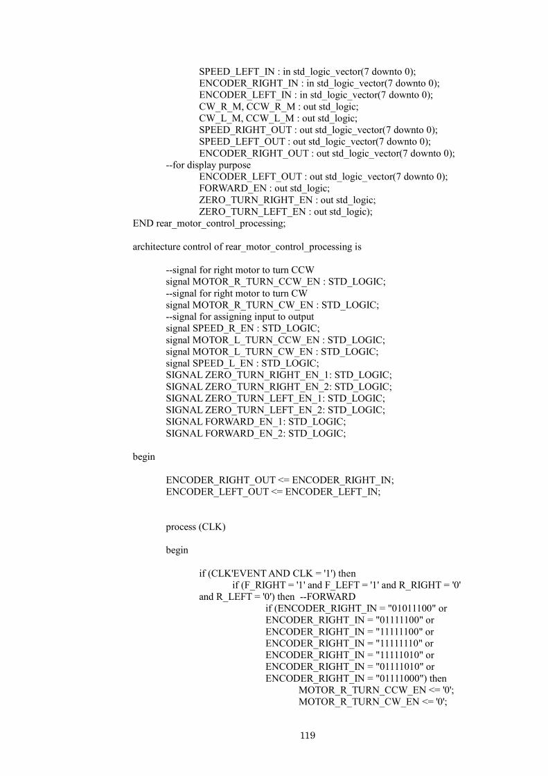
119
SPEED_LEFT_IN : in std_logic_vector(7 downto 0);
ENCODER_RIGHT_IN : in std_logic_vector(7 downto 0);
ENCODER_LEFT_IN : in std_logic_vector(7 downto 0);
CW_R_M, CCW_R_M : out std_logic;
CW_L_M, CCW_L_M : out std_logic;
SPEED_RIGHT_OUT : out std_logic_vector(7 downto 0);
SPEED_LEFT_OUT : out std_logic_vector(7 downto 0);
ENCODER_RIGHT_OUT : out std_logic_vector(7 downto 0);
--for display purpose
ENCODER_LEFT_OUT : out std_logic_vector(7 downto 0);
FORWARD_EN : out std_logic;
ZERO_TURN_RIGHT_EN : out std_logic;
ZERO_TURN_LEFT_EN : out std_logic);
END rear_motor_control_processing;
architecture control of rear_motor_control_processing is
--signal for right motor to turn CCW
signal MOTOR_R_TURN_CCW_EN : STD_LOGIC;
--signal for right motor to turn CW
signal MOTOR_R_TURN_CW_EN : STD_LOGIC;
--signal for assigning input to output
signal SPEED_R_EN : STD_LOGIC;
signal MOTOR_L_TURN_CCW_EN : STD_LOGIC;
signal MOTOR_L_TURN_CW_EN : STD_LOGIC;
signal SPEED_L_EN : STD_LOGIC;
SIGNAL ZERO_TURN_RIGHT_EN_1: STD_LOGIC;
SIGNAL ZERO_TURN_RIGHT_EN_2: STD_LOGIC;
SIGNAL ZERO_TURN_LEFT_EN_1: STD_LOGIC;
SIGNAL ZERO_TURN_LEFT_EN_2: STD_LOGIC;
SIGNAL FORWARD_EN_1: STD_LOGIC;
SIGNAL FORWARD_EN_2: STD_LOGIC;
begin
ENCODER_RIGHT_OUT <= ENCODER_RIGHT_IN;
ENCODER_LEFT_OUT <= ENCODER_LEFT_IN;
process (CLK)
begin
if (CLK'EVENT AND CLK = '1') then
if (F_RIGHT = '1' and F_LEFT = '1' and R_RIGHT = '0'
and R_LEFT = '0') then --FORWARD
if (ENCODER_RIGHT_IN = "01011100" or
ENCODER_RIGHT_IN = "01111100" or
ENCODER_RIGHT_IN = "11111100" or
ENCODER_RIGHT_IN = "11111110" or
ENCODER_RIGHT_IN = "11111010" or
ENCODER_RIGHT_IN = "01111010" or
ENCODER_RIGHT_IN = "01111000") then
MOTOR_R_TURN_CCW_EN <= '0';
MOTOR_R_TURN_CW_EN <= '0';

120
SPEED_R_EN <= '1';
FORWARD_EN_1 <= '1';
elsif (ENCODER_RIGHT_IN = "00011100" or
ENCODER_RIGHT_IN = "00011101" or
ENCODER_RIGHT_IN = "00011001") then
MOTOR_R_TURN_CCW_EN <= '0';
MOTOR_R_TURN_CW_EN <= '1';
SPEED_R_EN <= '1';
FORWARD_EN_1 <= '1';
else
MOTOR_R_TURN_CCW_EN <= '1';
MOTOR_R_TURN_CW_EN <= '0';
SPEED_R_EN <= '0';
FORWARD_EN_1 <= '0';
end if;
if (ENCODER_LEFT_IN = "00010000" or
ENCODER_LEFT_IN = "00110000" or
ENCODER_LEFT_IN = "00110001" or
ENCODER_LEFT_IN = "01110001" or
ENCODER_LEFT_IN = "01110000" or
ENCODER_LEFT_IN = "01110100" or
ENCODER_LEFT_IN = "01111100") then
MOTOR_L_TURN_CCW_EN <= '0';
MOTOR_L_TURN_CW_EN <= '0';
SPEED_L_EN <= '1';
FORWARD_EN_2 <= '1';
elsif (ENCODER_LEFT_IN = "10010000" or
ENCODER_LEFT_IN = "10010010" or
ENCODER_LEFT_IN = "10011010") then
MOTOR_L_TURN_CCW_EN <= '0';
MOTOR_L_TURN_CW_EN <= '1';
SPEED_L_EN <= '1';
FORWARD_EN_2 <= '1';
else
MOTOR_L_TURN_CCW_EN <= '1';
MOTOR_L_TURN_CW_EN <= '0';
SPEED_L_EN <= '0';
FORWARD_EN_2 <= '0';
end if;
FORWARD_EN <= (FORWARD_EN_1 AND
FORWARD_EN_2);
elsif (F_RIGHT = '0' and F_LEFT = '0' and R_RIGHT =
'1' and R_LEFT = '1') then --REVERSE
if (ENCODER_RIGHT_IN = "10010001" or
ENCODER_RIGHT_IN = "11010001" or
ENCODER_RIGHT_IN = "11000001" or
ENCODER_RIGHT_IN = "11000101" or
ENCODER_RIGHT_IN = "11000111" or
ENCODER_RIGHT_IN = "11001111" or
ENCODER_RIGHT_IN = "11101111" or
ENCODER_RIGHT_IN = "10101111") then
MOTOR_R_TURN_CCW_EN <= '0';
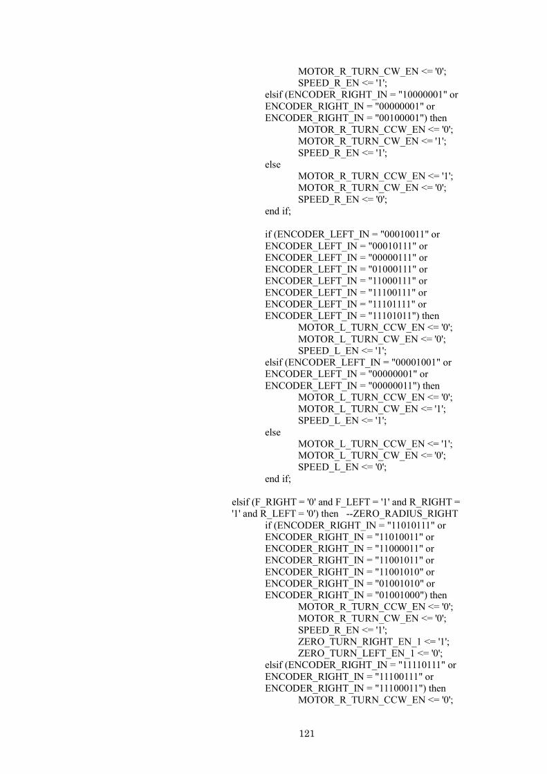
121
MOTOR_R_TURN_CW_EN <= '0';
SPEED_R_EN <= '1';
elsif (ENCODER_RIGHT_IN = "10000001" or
ENCODER_RIGHT_IN = "00000001" or
ENCODER_RIGHT_IN = "00100001") then
MOTOR_R_TURN_CCW_EN <= '0';
MOTOR_R_TURN_CW_EN <= '1';
SPEED_R_EN <= '1';
else
MOTOR_R_TURN_CCW_EN <= '1';
MOTOR_R_TURN_CW_EN <= '0';
SPEED_R_EN <= '0';
end if;
if (ENCODER_LEFT_IN = "00010011" or
ENCODER_LEFT_IN = "00010111" or
ENCODER_LEFT_IN = "00000111" or
ENCODER_LEFT_IN = "01000111" or
ENCODER_LEFT_IN = "11000111" or
ENCODER_LEFT_IN = "11100111" or
ENCODER_LEFT_IN = "11101111" or
ENCODER_LEFT_IN = "11101011") then
MOTOR_L_TURN_CCW_EN <= '0';
MOTOR_L_TURN_CW_EN <= '0';
SPEED_L_EN <= '1';
elsif (ENCODER_LEFT_IN = "00001001" or
ENCODER_LEFT_IN = "00000001" or
ENCODER_LEFT_IN = "00000011") then
MOTOR_L_TURN_CCW_EN <= '0';
MOTOR_L_TURN_CW_EN <= '1';
SPEED_L_EN <= '1';
else
MOTOR_L_TURN_CCW_EN <= '1';
MOTOR_L_TURN_CW_EN <= '0';
SPEED_L_EN <= '0';
end if;
elsif (F_RIGHT = '0' and F_LEFT = '1' and R_RIGHT =
'1' and R_LEFT = '0') then --ZERO_RADIUS_RIGHT
if (ENCODER_RIGHT_IN = "11010111" or
ENCODER_RIGHT_IN = "11010011" or
ENCODER_RIGHT_IN = "11000011" or
ENCODER_RIGHT_IN = "11001011" or
ENCODER_RIGHT_IN = "11001010" or
ENCODER_RIGHT_IN = "01001010" or
ENCODER_RIGHT_IN = "01001000") then
MOTOR_R_TURN_CCW_EN <= '0';
MOTOR_R_TURN_CW_EN <= '0';
SPEED_R_EN <= '1';
ZERO_TURN_RIGHT_EN_1 <= '1';
ZERO_TURN_LEFT_EN_1 <= '0';
elsif (ENCODER_RIGHT_IN = "11110111" or
ENCODER_RIGHT_IN = "11100111" or
ENCODER_RIGHT_IN = "11100011") then
MOTOR_R_TURN_CCW_EN <= '0';

122
MOTOR_R_TURN_CW_EN <= '1';
SPEED_R_EN <= '1';
ZERO_TURN_RIGHT_EN_1 <= '1';
ZERO_TURN_LEFT_EN_1 <= '0';
else
MOTOR_R_TURN_CCW_EN <= '1';
MOTOR_R_TURN_CW_EN <= '0';
SPEED_R_EN <= '0';
ZERO_TURN_RIGHT_EN_1 <= '0';
ZERO_TURN_LEFT_EN_1 <= '0';
end if;
if (ENCODER_LEFT_IN = "01001111" or
ENCODER_LEFT_IN = "01001101" or
ENCODER_LEFT_IN = "01001001" or
ENCODER_LEFT_IN = "01001000" or
ENCODER_LEFT_IN = "00001000" or
ENCODER_LEFT_IN = "00011000" or
ENCODER_LEFT_IN = "10011000") then
MOTOR_L_TURN_CCW_EN <= '0';
MOTOR_L_TURN_CW_EN <= '0';
SPEED_L_EN <= '1';
ZERO_TURN_RIGHT_EN_2 <= '1';
ZERO_TURN_LEFT_EN_2 <= '0';
elsif (ENCODER_LEFT_IN = "10101111" or
ENCODER_LEFT_IN = "00101111" or
ENCODER_LEFT_IN = "00001111") then
MOTOR_L_TURN_CCW_EN <= '0';
MOTOR_L_TURN_CW_EN <= '1';
SPEED_L_EN <= '1';
ZERO_TURN_RIGHT_EN_2 <= '1';
ZERO_TURN_LEFT_EN_2 <= '0';
else
MOTOR_L_TURN_CCW_EN <= '1';
MOTOR_L_TURN_CW_EN <= '0';
SPEED_L_EN <= '0';
ZERO_TURN_RIGHT_EN_2 <= '0';
ZERO_TURN_LEFT_EN_2 <= '0';
end if;
elsif (F_RIGHT = '1' and F_LEFT = '0' and R_RIGHT =
'0' and R_LEFT = '1') then --ZERO_RADIUS_LEFT
if (ENCODER_RIGHT_IN = "00111100" or
ENCODER_RIGHT_IN = "10111100" or
ENCODER_RIGHT_IN = "10101100" or
ENCODER_RIGHT_IN = "10100100" or
ENCODER_RIGHT_IN = "10100100" or
ENCODER_RIGHT_IN = "10000100" or
ENCODER_RIGHT_IN = "00000100" or
ENCODER_RIGHT_IN = "00000110" or
ENCODER_RIGHT_IN = "01000110") then
MOTOR_R_TURN_CCW_EN <= '0';
MOTOR_R_TURN_CW_EN <= '0';
SPEED_R_EN <= '1';
ZERO_TURN_LEFT_EN_1 <= '1';

123
ZERO_TURN_RIGHT_EN_1 <= '0';
elsif (ENCODER_RIGHT_IN = "00111101" or
ENCODER_RIGHT_IN = "01111101" or
ENCODER_RIGHT_IN = "01111111") then
MOTOR_R_TURN_CCW_EN <= '0';
MOTOR_R_TURN_CW_EN <= '1';
SPEED_R_EN <= '1';
ZERO_TURN_LEFT_EN_1 <= '1';
ZERO_TURN_RIGHT_EN_1 <= '0';
else
MOTOR_R_TURN_CCW_EN <= '1';
MOTOR_R_TURN_CW_EN <= '0';
SPEED_R_EN <= '0';
ZERO_TURN_LEFT_EN_1 <= '0';
ZERO_TURN_RIGHT_EN_1 <= '0';
end if;
if (ENCODER_LEFT_IN = "11110001" or
ENCODER_LEFT_IN = "11111001" or
ENCODER_LEFT_IN = "11111011" or
ENCODER_LEFT_IN = "11111010" or
ENCODER_LEFT_IN = "11110010" or
ENCODER_LEFT_IN = "11110000" or
ENCODER_LEFT_IN = "11110000" or
ENCODER_LEFT_IN = "11110100") then
MOTOR_L_TURN_CCW_EN <= '0';
MOTOR_L_TURN_CW_EN <= '0';
SPEED_L_EN <= '1';
ZERO_TURN_LEFT_EN_2 <= '1';
ZERO_TURN_RIGHT_EN_2 <= '0';
elsif (ENCODER_LEFT_IN = "11010001" or
ENCODER_LEFT_IN = "11000001" or
ENCODER_LEFT_IN = "11000101") then
MOTOR_L_TURN_CCW_EN <= '0';
MOTOR_L_TURN_CW_EN <= '1';
SPEED_L_EN <= '1';
ZERO_TURN_LEFT_EN_2 <= '1';
ZERO_TURN_RIGHT_EN_2 <= '0';
else
MOTOR_L_TURN_CCW_EN <= '1';
MOTOR_L_TURN_CW_EN <= '0';
SPEED_L_EN <= '0';
ZERO_TURN_LEFT_EN_2 <= '0';
ZERO_TURN_RIGHT_EN_2 <= '0';
end if;
else
MOTOR_R_TURN_CCW_EN <= '0';
MOTOR_R_TURN_CW_EN <= '0';
SPEED_R_EN <= '0';
MOTOR_L_TURN_CCW_EN <= '0';
MOTOR_L_TURN_CW_EN <= '0';
SPEED_L_EN <= '0';
end if;
end if;

124
end process;
ZERO_TURN_RIGHT_EN <= (ZERO_TURN_RIGHT_EN_1 AND
ZERO_TURN_RIGHT_EN_2);
ZERO_TURN_LEFT_EN <= (ZERO_TURN_LEFT_EN_1 AND
ZERO_TURN_LEFT_EN_2);
process (MOTOR_R_TURN_CCW_EN, MOTOR_R_TURN_CW_EN)
begin
if (MOTOR_R_TURN_CW_EN = '1' and
MOTOR_R_TURN_CCW_EN = '0') then
CW_R_M <= '1';
CCW_R_M <= '0';
elsif (MOTOR_R_TURN_CW_EN = '0' and
MOTOR_R_TURN_CCW_EN = '1') then
CW_R_M <= '0';
CCW_R_M <= '1';
else
CW_R_M <= '0';
CCW_R_M <= '0';
end if;
end process;
process (MOTOR_L_TURN_CCW_EN, MOTOR_L_TURN_CW_EN)
begin
if (MOTOR_L_TURN_CW_EN = '1' and
MOTOR_L_TURN_CCW_EN = '0') then
CW_L_M <= '1';
CCW_L_M <= '0';
elsif (MOTOR_L_TURN_CW_EN = '0' and
MOTOR_L_TURN_CCW_EN = '1') then
CW_L_M <= '0';
CCW_L_M <= '1';
else
CW_L_M <= '0';
CCW_L_M <= '0';
end if;
end process;
process (SPEED_R_EN, SPEED_L_EN)
begin
if (SPEED_R_EN = '1' and SPEED_L_EN = '1') then
SPEED_RIGHT_OUT <= SPEED_RIGHT_IN;
SPEED_LEFT_OUT <= SPEED_LEFT_IN;
else

125
SPEED_RIGHT_OUT <= "00000000";
SPEED_LEFT_OUT <= "00000000";
end if;
end process;
end control;
--signals selection block for autonomous or remote control operations
LIBRARY ieee;
USE ieee.std_logic_1164.all;
USE ieee.std_logic_unsigned.all;
USE ieee.std_logic_arith.all;
entity AUTO_REMOTE_SELECT is
port( clk : in std_logic;
remote_enable : in std_logic;
forward_right_motor_remote :in std_logic;--inputs from remote
reverse_right_motor_remote : in std_logic;
brake_right_motor_remote : in std_logic;
speed_data_right_motor_remote : in std_logic_vector (7 downto
0);
brake_data_right_motor_remote : in std_logic_vector (7 downto
0);
forward_left_motor_remote : in std_logic;
reverse_left_motor_remote : in std_logic;
brake_left_motor_remote : in std_logic;
speed_data_left_motor_remote : in std_logic_vector (7 downto
0);
brake_data_left_motor_remote : in std_logic_vector (7 downto
0);
auto_enable : in std_logic;
forward_right_motor_auto : in std_logic; --inputs from
autonomous module
reverse_right_motor_auto : in std_logic;
brake_right_motor_auto : in std_logic;
speed_data_right_motor_auto : in std_logic_vector (7 downto
0);
brake_data_right_motor_auto : in std_logic_vector (7 downto
0);
forward_left_motor_auto : in std_logic;
reverse_left_motor_auto : in std_logic;
brake_left_motor_auto : in std_logic;
speed_data_left_motor_auto : in std_logic_vector (7 downto 0);
brake_data_left_motor_auto : in std_logic_vector (7 downto 0);
forward_right_motor : out std_logic;
reverse_right_motor : out std_logic;
brake_right_motor : out std_logic;
speed_data_right_motor : out std_logic_vector (7 downto 0);
brake_data_right_motor : out std_logic_vector (7 downto 0);
forward_left_motor : out std_logic;
reverse_left_motor : out std_logic;
brake_left_motor : out std_logic;
speed_data_left_motor : out std_logic_vector (7 downto 0);
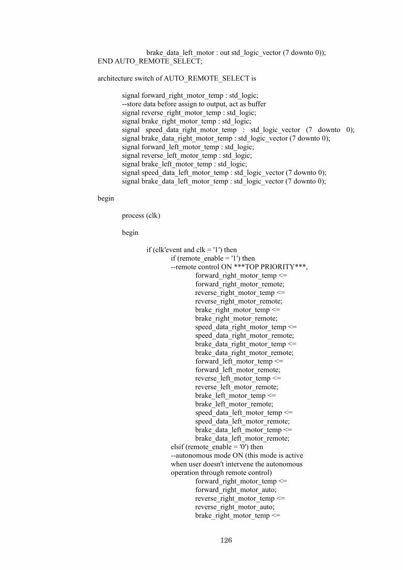
126
brake_data_left_motor : out std_logic_vector (7 downto 0));
END AUTO_REMOTE_SELECT;
architecture switch of AUTO_REMOTE_SELECT is
signal forward_right_motor_temp : std_logic;
--store data before assign to output, act as buffer
signal reverse_right_motor_temp : std_logic;
signal brake_right_motor_temp : std_logic;
signal speed_data_right_motor_temp : std_logic_vector (7 downto 0);
signal brake_data_right_motor_temp : std_logic_vector (7 downto 0);
signal forward_left_motor_temp : std_logic;
signal reverse_left_motor_temp : std_logic;
signal brake_left_motor_temp : std_logic;
signal speed_data_left_motor_temp : std_logic_vector (7 downto 0);
signal brake_data_left_motor_temp : std_logic_vector (7 downto 0);
begin
process (clk)
begin
if (clk'event and clk = '1') then
if (remote_enable = '1') then
--remote control ON ***TOP PRIORITY***,
forward_right_motor_temp <=
forward_right_motor_remote;
reverse_right_motor_temp <=
reverse_right_motor_remote;
brake_right_motor_temp <=
brake_right_motor_remote;
speed_data_right_motor_temp <=
speed_data_right_motor_remote;
brake_data_right_motor_temp <=
brake_data_right_motor_remote;
forward_left_motor_temp <=
forward_left_motor_remote;
reverse_left_motor_temp <=
reverse_left_motor_remote;
brake_left_motor_temp <=
brake_left_motor_remote;
speed_data_left_motor_temp <=
speed_data_left_motor_remote;
brake_data_left_motor_temp <=
brake_data_left_motor_remote;
elsif (remote_enable = '0') then
--autonomous mode ON (this mode is active
when user doesn't intervene the autonomous
operation through remote control)
forward_right_motor_temp <=
forward_right_motor_auto;
reverse_right_motor_temp <=
reverse_right_motor_auto;
brake_right_motor_temp <=
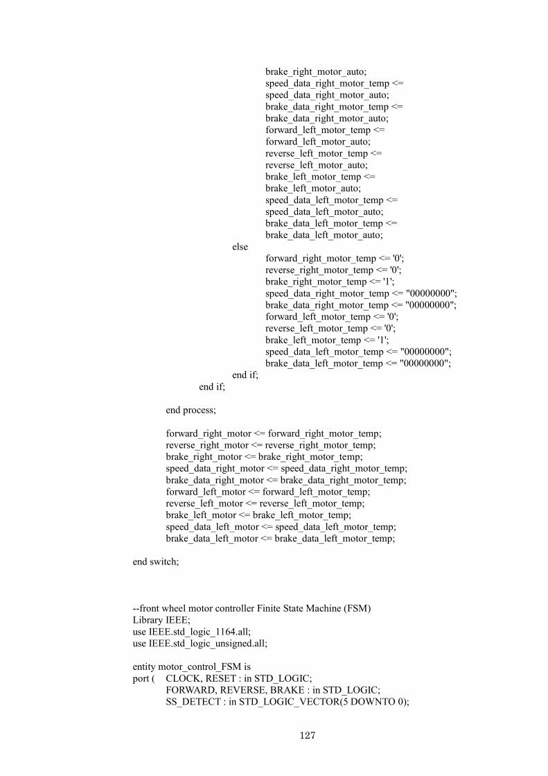
127
brake_right_motor_auto;
speed_data_right_motor_temp <=
speed_data_right_motor_auto;
brake_data_right_motor_temp <=
brake_data_right_motor_auto;
forward_left_motor_temp <=
forward_left_motor_auto;
reverse_left_motor_temp <=
reverse_left_motor_auto;
brake_left_motor_temp <=
brake_left_motor_auto;
speed_data_left_motor_temp <=
speed_data_left_motor_auto;
brake_data_left_motor_temp <=
brake_data_left_motor_auto;
else
forward_right_motor_temp <= '0';
reverse_right_motor_temp <= '0';
brake_right_motor_temp <= '1';
speed_data_right_motor_temp <= "00000000";
brake_data_right_motor_temp <= "00000000";
forward_left_motor_temp <= '0';
reverse_left_motor_temp <= '0';
brake_left_motor_temp <= '1';
speed_data_left_motor_temp <= "00000000";
brake_data_left_motor_temp <= "00000000";
end if;
end if;
end process;
forward_right_motor <= forward_right_motor_temp;
reverse_right_motor <= reverse_right_motor_temp;
brake_right_motor <= brake_right_motor_temp;
speed_data_right_motor <= speed_data_right_motor_temp;
brake_data_right_motor <= brake_data_right_motor_temp;
forward_left_motor <= forward_left_motor_temp;
reverse_left_motor <= reverse_left_motor_temp;
brake_left_motor <= brake_left_motor_temp;
speed_data_left_motor <= speed_data_left_motor_temp;
brake_data_left_motor <= brake_data_left_motor_temp;
end switch;
--front wheel motor controller Finite State Machine (FSM)
Library IEEE;
use IEEE.std_logic_1164.all;
use IEEE.std_logic_unsigned.all;
entity motor_control_FSM is
port ( CLOCK, RESET : in STD_LOGIC;
FORWARD, REVERSE, BRAKE : in STD_LOGIC;
SS_DETECT : in STD_LOGIC_VECTOR(5 DOWNTO 0);

128
SPEED_DATA_IN, BRAKE_DATA_IN : in STD_LOGIC_VECTOR(7
DOWNTO 0);
RPM : in STD_LOGIC_VECTOR(11 DOWNTO 0);
--to make sure that rpm=0 then only can change direction
STATE : out STD_LOGIC_VECTOR(2 DOWNTO 0);
SPEED_DATA_OUT, BRAKE_DATA_OUT : out
STD_LOGIC_VECTOR(7 DOWNTO 0));
end motor_control_FSM;
architecture BEHV of motor_control_FSM is
type STATE_TYPE is (F, R, B, CA, CB);
--F=FORWARD, R=REVERSE, B=BRAKE
signal CS, NS: STATE_TYPE;
signal FRB: STD_LOGIC_VECTOR(2 DOWNTO 0);
signal SPEED: STD_LOGIC_VECTOR(7 DOWNTO 0);
signal STOP: STD_LOGIC_VECTOR(7 DOWNTO 0);
signal RPM_TEMP: STD_LOGIC_VECTOR(11 DOWNTO 0);
signal SS_DETECT_TEMP : STD_LOGIC_VECTOR(5 DOWNTO 0);
begin
FRB(2) <= FORWARD;
FRB(1) <= REVERSE;
FRB(0) <= BRAKE;
SPEED <= SPEED_DATA_IN;
STOP <= BRAKE_DATA_IN;
SYNC_PROC: process (CLOCK, RESET)
begin
if (RESET='1') then
CS <= B;
elsif (CLOCK'event and CLOCK = '1') then
CS <= NS;
RPM_TEMP <= RPM;
SS_DETECT_TEMP <= SS_DETECT;
end if;
end process; --End REG_PROC
COMB_PROC: process (CS, FRB)
begin
case CS is
--CS=current, NS=next, F=forward, B=brake, R=reverse, CA=clear DAC
channel A, CB=clear DAC channel B
when B =>
if (RPM_TEMP = "000000000000") then --check on the rpm so that
motor only change direction when rpm=0
if (SS_DETECT_TEMP = "000111") then
if (FRB = "100") then
NS <= CB;
elsif (FRB = "010") then
NS <= CB;
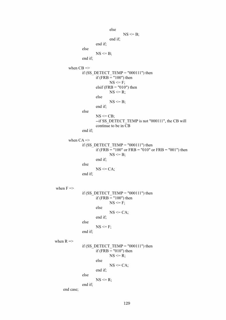
129
else
NS <= B;
end if;
end if;
else
NS <= B;
end if;
when CB =>
if (SS_DETECT_TEMP = "000111") then
if (FRB = "100") then
NS <= F;
elsif (FRB = "010") then
NS <= R;
else
NS <= B;
end if;
else
NS <= CB;
--if SS_DETECT_TEMP is not "000111", the CB will
continue to be in CB
end if;
when CA =>
if (SS_DETECT_TEMP = "000111") then
if (FRB = "100" or FRB = "010" or FRB = "001") then
NS <= B;
end if;
else
NS <= CA;
end if;
when F =>
if (SS_DETECT_TEMP = "000111") then
if (FRB = "100") then
NS <= F;
else
NS <= CA;
end if;
else
NS <= F;
end if;
when R =>
if (SS_DETECT_TEMP = "000111") then
if (FRB = "010") then
NS <= R;
else
NS <= CA;
end if;
else
NS <= R;
end if;
end case;

130
end process; -- End COMB_PROC
STATE_PROC: process (CS)
begin
case CS is
when B =>
STATE <= "000"; --"000" output will indicate
BRAKE in the next module
SPEED_DATA_OUT <= SPEED;
BRAKE_DATA_OUT <= STOP;
when F =>
STATE <= "010";--"010" output will indicate
FORWARD in the next module
SPEED_DATA_OUT <= SPEED;
BRAKE_DATA_OUT <= STOP;
when R =>
STATE <= "011";--"011" output will indicate
REVERSE in the next module
SPEED_DATA_OUT <= SPEED;
BRAKE_DATA_OUT <= STOP;
when CA =>
STATE <= "100";--"100" output will indicate
CLEAR DAC CHANNEL A in the next module
SPEED_DATA_OUT <= SPEED;
BRAKE_DATA_OUT <= STOP;
when CB =>
STATE <= "001";--"100" output will indicate
CLEAR DAC CHANNEL B in the next module
SPEED_DATA_OUT <= SPEED;
BRAKE_DATA_OUT <= STOP;
end case;
end process;
end BEHV;
--motor controller data arrangement for SPI communication
Library IEEE;
use IEEE.std_logic_1164.all;
use IEEE.std_logic_unsigned.all;
entity motor_controller_left is
port ( CLOCK, SS : in STD_LOGIC;
STATE : in STD_LOGIC_VECTOR(2 DOWNTO 0);
SPEED_DATA_IN, BRAKE_DATA_IN : in STD_LOGIC_VECTOR(7
DOWNTO 0);
SS_DETECT : out STD_LOGIC_VECTOR(5 DOWNTO 0); --output for
motor FSM
THROTTLE : out STD_LOGIC;
REVERSE : out STD_LOGIC;
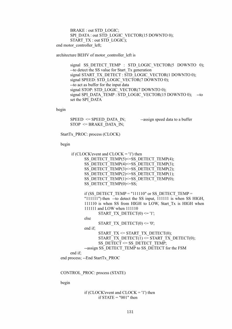
131
BRAKE : out STD_LOGIC;
SPI_DATA : out STD_LOGIC_VECTOR(15 DOWNTO 0);
START_TX : out STD_LOGIC);
end motor_controller_left;
architecture BEHV of motor_controller_left is
signal SS_DETECT_TEMP : STD_LOGIC_VECTOR(5 DOWNTO 0);
--to detect the SS value for Start_Tx generation
signal START_TX_DETECT : STD_LOGIC_VECTOR(1 DOWNTO 0);
signal SPEED: STD_LOGIC_VECTOR(7 DOWNTO 0);
--to act as buffer for the input data
signal STOP: STD_LOGIC_VECTOR(7 DOWNTO 0);
signal SPI_DATA_TEMP : STD_LOGIC_VECTOR(15 DOWNTO 0); --to
set the SPI_DATA
begin
SPEED <= SPEED_DATA_IN; --assign speed data to a buffer
STOP <= BRAKE_DATA_IN;
StartTx_PROC: process (CLOCK)
begin
if (CLOCK'event and CLOCK = '1') then
SS_DETECT_TEMP(5)<=SS_DETECT_TEMP(4);
SS_DETECT_TEMP(4)<=SS_DETECT_TEMP(3);
SS_DETECT_TEMP(3)<=SS_DETECT_TEMP(2);
SS_DETECT_TEMP(2)<=SS_DETECT_TEMP(1);
SS_DETECT_TEMP(1)<=SS_DETECT_TEMP(0);
SS_DETECT_TEMP(0)<=SS;
if (SS_DETECT_TEMP = "111110" or SS_DETECT_TEMP =
"111111") then --to detect the SS input, 111111 is when SS HIGH,
111110 is when SS from HIGH to LOW, Start_Tx is HIGH when
111111 and LOW when 111110
START_TX_DETECT(0) <= '1';
else
START_TX_DETECT(0) <= '0';
end if;
START_TX <= START_TX_DETECT(0);
START_TX_DETECT(1) <= START_TX_DETECT(0);
SS_DETECT <= SS_DETECT_TEMP;
--assign SS_DETECT_TEMP to SS_DETECT for the FSM
end if;
end process; --End StartTx_PROC
CONTROL_PROC: process (STATE)
begin
if (CLOCK'event and CLOCK = '1') then
if STATE = "001" then
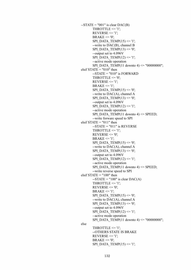
132
--STATE = "001" is clear DAC(B)
THROTTLE <= '1';
REVERSE <= '1';
BRAKE <= '0';
SPI_DATA_TEMP(15) <= '1';
--write to DAC(B), channel B
SPI_DATA_TEMP(13) <= '0';
--output set to 4.096V
SPI_DATA_TEMP(12) <= '1';
--active mode operation
SPI_DATA_TEMP(11 downto 4) <= "00000000";
elsif STATE = "010" then
--STATE = "010" is FORWARD
THROTTLE <= '0';
REVERSE <= '1';
BRAKE <= '1';
SPI_DATA_TEMP(15) <= '0';
--write to DAC(A), channel A
SPI_DATA_TEMP(13) <= '0';
--output set to 4.096V
SPI_DATA_TEMP(12) <= '1';
--active mode operation
SPI_DATA_TEMP(11 downto 4) <= SPEED;
--write forware speed to SPI
elsif STATE = "011" then
--STATE = "011" is REVERSE
THROTTLE <= '1';
REVERSE <= '0';
BRAKE <= '1';
SPI_DATA_TEMP(15) <= '0';
--write to DAC(A), channel A
SPI_DATA_TEMP(13) <= '0';
--output set to 4.096V
SPI_DATA_TEMP(12) <= '1';
--active mode operation
SPI_DATA_TEMP(11 downto 4) <= SPEED;
--write reverse speed to SPI
elsif STATE = "100" then
--STATE = "100" is clear DAC(A)
THROTTLE <= '1';
REVERSE <= '0';
BRAKE <= '1';
SPI_DATA_TEMP(15) <= '0';
--write to DAC(A), channel A
SPI_DATA_TEMP(13) <= '0';
--output set to 4.096V
SPI_DATA_TEMP(12) <= '1';
--active mode operation
SPI_DATA_TEMP(11 downto 4) <= "00000000";
else
THROTTLE <= '1';
--OTHERS STATE IS BRAKE
REVERSE <= '1';
BRAKE <= '0';
SPI_DATA_TEMP(15) <= '1';

133
--write to DAC(A), channel B
SPI_DATA_TEMP(13) <= '0';
--output set to 4.096V
SPI_DATA_TEMP(12) <= '1';
--active mode operation
SPI_DATA_TEMP(11 downto 4) <= STOP;
--write stop data to SPI
end if;
end if;
end process; --End CONTROL_PROC
SPI_PROC: process (START_TX_DETECT)
begin
if START_TX_DETECT = "01" then
SPI_DATA <= SPI_DATA_TEMP;
else
SPI_DATA_TEMP <= SPI_DATA_TEMP;
end if;
end process; --End SPI_PROC
end BEHV;
--SPI communication
library ieee;
use ieee.std_logic_1164.all;
use ieee.numeric_std.all;
entity simpleSPI_M is
port (
reset : in std_logic;
clk : in std_logic;
SCLK : inout std_logic;
SS : out std_logic;
MOSI : out std_logic;
--output from MSB to LSB to suit the DAC requirements
MISO : in std_logic;
DataToTx : in std_logic_vector(15 downto 0);
DataRxd : out std_logic_vector(15 downto 0);
StartTx : in std_logic);
--it has to be high to start transmitting, low after finish
end simpleSPI_M;
architecture a of simpleSPI_M is
type state_type is (idle, loadData, delay1, txBit, CheckFinished);
signal state : state_type;
begin
process(clk, reset, StartTx)
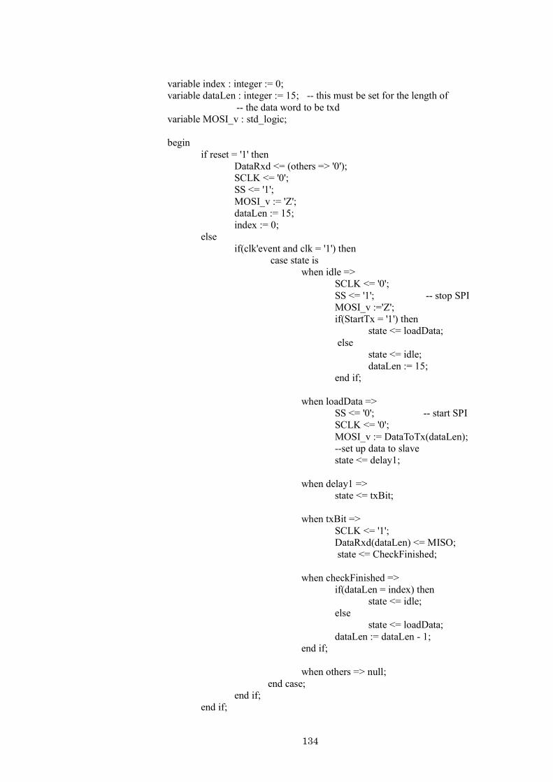
134
variable index : integer := 0;
variable dataLen : integer := 15; -- this must be set for the length of
-- the data word to be txd
variable MOSI_v : std_logic;
begin
if reset = '1' then
DataRxd <= (others => '0');
SCLK <= '0';
SS <= '1';
MOSI_v := 'Z';
dataLen := 15;
index := 0;
else
if(clk'event and clk = '1') then
case state is
when idle =>
SCLK <= '0';
SS <= '1'; -- stop SPI
MOSI_v :='Z';
if(StartTx = '1') then
state <= loadData;
else
state <= idle;
dataLen := 15;
end if;
when loadData =>
SS <= '0'; -- start SPI
SCLK <= '0';
MOSI_v := DataToTx(dataLen);
--set up data to slave
state <= delay1;
when delay1 =>
state <= txBit;
when txBit =>
SCLK <= '1';
DataRxd(dataLen) <= MISO;
state <= CheckFinished;
when checkFinished =>
if(dataLen = index) then
state <= idle;
else
state <= loadData;
dataLen := dataLen - 1;
end if;
when others => null;
end case;
end if;
end if;
135
MOSI <= MOSI_v; --most significant bit MSB will be ouput first
end process;
end a;
--motor RPM counter
LIBRARY ieee;
USE ieee.std_logic_1164.all;
USE ieee.std_logic_unsigned.all;
USE ieee.std_logic_arith.all;
entity rotary_encoder_right is
port( rotary_in : in std_logic;
clk : in std_logic;
reset : in std_logic;
rpm_count : out std_logic_vector (11 downto 0)); --count in
revolution per minute (8 input pulses is one revolution)
end rotary_encoder_right;
architecture rotary_count of rotary_encoder_right is
signal pulse_count : std_logic_vector (3 downto 0); --pulse_count will
count the number of input pulse
signal revolution_count : std_logic_vector (7 downto 0); --revolution_count
will count the number of revolution, 8 pulses is equal to one revolution
signal rpm_count_temp : std_logic_vector (14 downto 0);
signal clk_count : std_logic_vector (16 downto 0); --it counts the clk
(27Mhz/256) to get 1s (1 second)
begin
process(reset,clk)
variable detect : std_ulogic_vector (1 downto 0);
begin
if reset ='1' then
detect := "00";
pulse_count <= "0000";
revolution_count <= "00000000";
clk_count <= "00000000000000000"; --for 1s
elsif rising_edge(clk) then
detect(1) := detect(0); -- record last value of rotary_in in
detect(1)
detect(0) := rotary_in ; --record current rotary_in in detect(0)
clk_count <= clk_count + '1';
if (clk_count < "11001110000010010") then -- clk count for 1s,
so encoder will have ouput every 1s
if detect = "01" then -- rising_edge
pulse_count <= pulse_count + '1';
elsif detect = "10" then --falling_edge
pulse_count <= pulse_count;

136
if pulse_count = "1000" then
--if pulses count = 8, revolution count add 1
revolution_count <= revolution_count + '1';
pulse_count <= "0000";
else
revolution_count <= revolution_count;
end if;
end if;
elsif (clk_count = "11001110000010010") then
rpm_count_temp <= revolution_count * "0111100"; --
revolution_count in 1s x 60 = revolution per minute (111100
= 60)
revolution_count <= "00000000";
clk_count <= "00000000000000000"; --for 1s
end if;
end if;
rpm_count <= rpm_count_temp (11 downto 0);
end process;
end rotary_count;
--Ultrasonic sensors modules distance normalization
LIBRARY ieee;
USE ieee.std_logic_1164.all;
entity distance_FP_normalize is
port( FP: in std_logic_vector (31 downto 0);
normalize_integer: out std_logic_vector (3 downto 0);
normalize_fraction: out std_logic_vector (4 downto 0));
end distance_FP_normalize;
architecture normalize of distance_FP_normalize is
signal mantissa: std_logic_vector (22 downto 0);
begin
process (FP)
begin
mantissa <= '1' & FP (22 downto 1); -- normalize the mantissa by
adding '1' before mantissa
if (FP (30 downto 23) > "10000001") then-- exponent > 129
normalize_integer <= "0110"; -- display 6.5 for any
value larger than 6.5 since maximum Max Sonar
range is 6.5 meter
normalize_fraction <= "01111";
elsif (FP (30 downto 23) = "10000001") then --exponent =
129
normalize_integer <= '0' & mantissa (22 downto 20);
normalize_fraction <= mantissa (19 downto 15);
elsif (FP (30 downto 23) = "10000000") then -- exponent =
137
128
normalize_integer <= "00" & mantissa (22 downto
21);
normalize_fraction <= mantissa (20 downto 16);
elsif (FP (30 downto 23) = "01111111") then -- exponent =
127
normalize_integer <= "000" & mantissa (22);
normalize_fraction <= mantissa (21 downto 17);
elsif (FP (30 downto 23) = "01111110") then -- exponent =
126
normalize_integer <= "0000";
normalize_fraction <= mantissa (22 downto 18);
elsif (FP (30 downto 23) = "01111101") then -- exponent =
125
normalize_integer <= "0000";
normalize_fraction <= '0' & mantissa (22 downto
19);
elsif (FP (30 downto 23) = "01111100") then -- exponent
= 124
normalize_integer <= "0000";
normalize_fraction <= "00" & mantissa (22 downto
20);
elsif (FP (30 downto 23) = "01111011") then -- exponent =
123
normalize_integer <= "0000";
normalize_fraction <= "000" & mantissa (22 downto
21);
elsif (FP (30 downto 23) = "01111010") then -- exponent =
122
normalize_integer <= "0000";
normalize_fraction <= "0000" & mantissa (22);
else
normalize_integer <= "1000"; --display 8 for
exponent < 122
normalize_fraction <= "11010"; --display 8 for
exponent < 122
end if;
end process;
end normalize;
--autonomous navigation module
Library IEEE;
use IEEE.std_logic_1164.all;
use IEEE.std_logic_unsigned.all;
entity autonomous_navigation is
port ( CLOCK,Start : in STD_LOGIC;
sonar_right_data_Ready : in STD_LOGIC;
sonar_left_data_Ready : in STD_LOGIC;
sonar_center_data_Ready : in STD_LOGIC;
zero_radius_right_ready : in STD_LOGIC;
forward_ready : in STD_LOGIC;
138
zero_turn_right_ready : in STD_LOGIC;
zero_turn_left_ready : in STD_LOGIC;
sonar_integer_right : in STD_LOGIC_VECTOR(3 DOWNTO 0);
sonar_integer_left : in STD_LOGIC_VECTOR(3 DOWNTO 0);
sonar_integer_center : in STD_LOGIC_VECTOR(3 DOWNTO 0);
pulse_count_left : in STD_LOGIC_VECTOR(3 DOWNTO 0);
GPS_in : in STD_LOGIC_VECTOR(7 DOWNTO 0);
vision_in : in STD_LOGIC_VECTOR(7 DOWNTO 0);
obstacle_out : out std_logic;
turn_right_done_out : out std_logic;
reset_pulse_count_left : out std_logic;
sonar_right_Request : out std_logic;
sonar_left_Request : out std_logic;
sonar_center_Request : out std_logic;
F_RIGHT, R_RIGHT, B_RIGHT : out std_logic;
SPEED_RIGHT_OUT, BRAKE_RIGHT_OUT : out std_logic_vector(7
downto 0);
F_LEFT, R_LEFT, B_LEFT : out std_logic;
SPEED_LEFT_OUT, BRAKE_LEFT_OUT : out std_logic_vector(7 downto
0));
end autonomous_navigation;
architecture navigation of autonomous_navigation is
signal SPEED_RIGHT_OUT_temp, BRAKE_RIGHT_OUT_temp,
SPEED_LEFT_OUT_temp, BRAKE_LEFT_OUT_temp :
STD_LOGIC_VECTOR(7 DOWNTO 0);
begin
--high level navigation, GPS, IMU and Vision data can be integrated here
process (sonar_center_data_Ready)
begin
if (sonar_center_data_Ready = '1') then
if (sonar_integer_center > 0010) then
F_RIGHT <= '1';
R_RIGHT <= '0';
B_RIGHT <= '0';
SPEED_RIGHT_OUT_temp <= "01000000";
BRAKE_RIGHT_OUT_temp <= "00000000";
F_LEFT <= '1';
R_LEFT <= '0';
B_LEFT <= '0';
SPEED_LEFT_OUT_temp <= "01000000";
BRAKE_LEFT_OUT_temp <= "00000000";
elsif (sonar_integer_center > 0010) then
F_RIGHT <= '0';
R_RIGHT <= '0';
B_RIGHT <= '1';
SPEED_RIGHT_OUT_temp <= "00000000";
BRAKE_RIGHT_OUT_temp <= "01000000";
F_LEFT <= '0';
R_LEFT <= '0';
B_LEFT <= '1';

139
SPEED_LEFT_OUT_temp <= "00000000";
BRAKE_LEFT_OUT_temp <= "01000000";
else
F_RIGHT <= '0';
R_RIGHT <= '0';
B_RIGHT <= '1';
SPEED_RIGHT_OUT_temp <= "00000000";
BRAKE_RIGHT_OUT_temp <= "01000000";
F_LEFT <= '0';
R_LEFT <= '0';
B_LEFT <= '1';
SPEED_LEFT_OUT_temp <= "00000000";
BRAKE_LEFT_OUT_temp <= "01000000";
end if;
else
F_RIGHT <= '0';
R_RIGHT <= '0';
B_RIGHT <= '1';
SPEED_RIGHT_OUT_temp <= "00000000";
BRAKE_RIGHT_OUT_temp <= "01000000";
F_LEFT <= '0';
R_LEFT <= '0';
B_LEFT <= '1';
SPEED_LEFT_OUT_temp <= "00000000";
BRAKE_LEFT_OUT_temp <= "01000000";
end if;
end process;
SPEED_RIGHT_OUT <= SPEED_RIGHT_OUT_temp;
BRAKE_RIGHT_OUT <= BRAKE_RIGHT_OUT_temp;
SPEED_LEFT_OUT <= SPEED_LEFT_OUT_temp;
BRAKE_LEFT_OUT <= BRAKE_LEFT_OUT_temp;
end navigation;
--GPS receiver module UART
// RS-232 RX module
module GPS_Module(clk, RxD, RxD_data_ready, RxD_data, RxD_endofpacket,
RxD_idle);
input clk, RxD;
output RxD_data_ready; // onc clock pulse when RxD_data is valid
output [7:0] RxD_data;
parameter ClkFrequency = 27000000; // 27MHz
parameter Baud =4800;
output RxD_endofpacket; // one clock pulse, when no more data is received
(RxD_idle is going high)
output RxD_idle; // no data is being received
// Baud generator (we use 8 times oversampling)

140
parameter Baud8 = Baud*8;
parameter Baud8GeneratorAccWidth = 8;
wire [Baud8GeneratorAccWidth:0] Baud8GeneratorInc =
((Baud8<<(Baud8GeneratorAccWidth-7))+(ClkFrequency>>8))/(ClkFrequency>>7);
reg [Baud8GeneratorAccWidth:0] Baud8GeneratorAcc;
always @(posedge clk)
Baud8GeneratorAcc <= Baud8GeneratorAcc[Baud8GeneratorAccWidth-1:0] +
Baud8GeneratorInc;
wire Baud8Tick = Baud8GeneratorAcc[Baud8GeneratorAccWidth];
reg [1:0] RxD_sync_inv;
always @(posedge clk)
if(Baud8Tick)
RxD_sync_inv <= {RxD_sync_inv[0], ~RxD};
reg [1:0] RxD_cnt_inv;
reg RxD_bit_inv;
always @(posedge clk)
if(Baud8Tick)
begin
if( RxD_sync_inv[1] && RxD_cnt_inv!=2'b11)
RxD_cnt_inv <= RxD_cnt_inv + 2'h1;
else
if(~RxD_sync_inv[1] && RxD_cnt_inv!=2'b00)
RxD_cnt_inv <= RxD_cnt_inv - 2'h1;
if(RxD_cnt_inv==2'b00)
RxD_bit_inv <= 1'b0;
else
if(RxD_cnt_inv==2'b11) RxD_bit_inv <= 1'b1;
end
reg [3:0] state;
reg [3:0] bit_spacing;
// "next_bit" controls when the data sampling occurs
// depending on how noisy the RxD is, different values might work better
// with a clean connection, values from 8 to 11 work
wire next_bit = (bit_spacing==4'd11);
always @(posedge clk)
if(state==0)
bit_spacing <= 4'b0000;
else
if(Baud8Tick)
bit_spacing <= {bit_spacing[2:0]+4'b0001}| {bit_spacing[3],
3'b000};
always @(posedge clk)
if(Baud8Tick)

141
case(state)
4'b0000: if(RxD_bit_inv) state <= 4'b1000; // start bit found?
4'b1000: if(next_bit) state <= 4'b1001; // bit 0
4'b1001: if(next_bit) state <= 4'b1010; // bit 1
4'b1010: if(next_bit) state <= 4'b1011; // bit 2
4'b1011: if(next_bit) state <= 4'b1100; // bit 3
4'b1100: if(next_bit) state <= 4'b1101; // bit 4
4'b1101: if(next_bit) state <= 4'b1110; // bit 5
4'b1110: if(next_bit) state <= 4'b1111; // bit 6
4'b1111: if(next_bit) state <= 4'b0001; // bit 7
4'b0001: if(next_bit) state <= 4'b0000; // stop bit
default: state <= 4'b0000;
endcase
reg [7:0]RxD_data;
always @(posedge RxD_data_ready)
RxD_data=RxD_data_r;
reg [7:0] RxD_data_r;
always @(posedge clk)
if(Baud8Tick && next_bit && state[3])
RxD_data_r <= {~RxD_bit_inv, RxD_data_r[7:1]};
reg RxD_data_ready, RxD_data_error;
always @(posedge clk)
begin
RxD_data_ready <= (Baud8Tick && next_bit && state==4'b0001
&& ~RxD_bit_inv); // ready only if the stop bit is received
RxD_data_error <= (Baud8Tick && next_bit && state==4'b0001
&& RxD_bit_inv); // error if the stop bit is not received
end
reg [4:0] gap_count;
always @(posedge clk)
if (state!=0)
gap_count<=5'h00;
else if(Baud8Tick & ~gap_count[4])
gap_count <= gap_count + 5'h01;
assign RxD_idle = gap_count[4];
reg RxD_endofpacket;
always @(posedge clk)
RxD_endofpacket <= Baud8Tick & (gap_count==5'h0F);
Endmodule
--a call to Sobel edge detection function, this part is inserted to top-level entity
// sobel
wire [9:0] wVGA_R = Read_DATA2[9:0];
wire [9:0] wVGA_G = {Read_DATA1[14:10],Read_DATA2[14:10]};
wire [9:0] wVGA_B = Read_DATA1[9:0];
142
// sobel
wire wDVAL_sobel;
wire [9:0] wSobel;
sobel_edge_detection sobel0 (
.iCLK(VGA_CTRL_CLK),
.iRST_N(DLY_RST_2),
.iTHRESHOLD({SW[7:2],2'b0}),
.iDVAL(Read), //Read is request from VGA_Control
.iDATA(wVGA_G), // gray
.oDVAL(wDAL_sobel),
.oDATA(wSobel)
);
// gray
wire [9:0] wGray_R = wVGA_G;
wire [9:0] wGray_G = wVGA_G;
wire [9:0] wGray_B = wVGA_G;
// to display
wire [9:0] wDISP_R = SW[9] ? wGray_R : // Gray
SW[8] ? wSobel : // Sobel
wVGA_R; // Color
wire [9:0] wDISP_G = SW[9] ? wGray_G : // Gray
SW[8] ? wSobel : // Sobel
wVGA_G; // Color
wire [9:0] wDISP_B = SW[9] ? wGray_B : // Gray
SW[8] ? wSobel : // Sobel
wVGA_B; // Color
--Sobel edge detection
module sobel_edge_detection (
input iRST_N,
input iCLK,
input [7:0] iTHRESHOLD,
input iDVAL,
input [9:0] iDATA,
output reg oDVAL,
output reg [9:0] oDATA
);
// coefficient x
parameter X1 = 8'hff, X2 = 8'h00, X3 = 8'h01;
parameter X4 = 8'hfe, X5 = 8'h00, X6 = 8'h02;
parameter X7 = 8'hff, X8 = 8'h00, X9 = 8'h01;
// coefficient y
parameter Y1 = 8'h01, Y2 = 8'h02, Y3 = 8'h01;
parameter Y4 = 8'h00, Y5 = 8'h00, Y6 = 8'h00;
parameter Y7 = 8'hff, Y8 = 8'hfe, Y9 = 8'hff;
wire [7:0] Line0;

143
wire [7:0] Line1;
wire [7:0] Line2;
wire [17:0] mac_x0;
wire [17:0] mac_x1;
wire [17:0] mac_x2;
wire [17:0] mac_y0;
wire [17:0] mac_y1;
wire [17:0] mac_y2;
wire [19:0] pa_x;
wire [19:0] pa_y;
wire [15:0] abs_mag;
line_buffer_3 b0 (
.clken(iDVAL),
.clock(iCLK),
.shiftin(iDATA[9:2]),
.taps0x(Line0),
.taps1x(Line1),
.taps2x(Line2)
);
// X
mult_add_3 x0 (
.aclr0(!iRST_N),
.clock0(iCLK),
.dataa_0(Line0),
.datab_0(X9),
.datab_1(X8),
.datab_2(X7),
.result(mac_x0)
);
mult_add_3 x1 (
.aclr0(!iRST_N),
.clock0(iCLK),
.dataa_0(Line1),
.datab_0(X6),
.datab_1(X5),
.datab_2(X4),
.result(mac_x1)
);
mult_add_3 x2 (
.aclr0(!iRST_N),
.clock0(iCLK),
.dataa_0(Line2),
.datab_0(X3),
.datab_1(X2),
.datab_2(X1),
.result(mac_x2)
);

144
// Y
mult_add_3 y0 (
.aclr0(!iRST_N),
.clock0(iCLK),
.dataa_0(Line0),
.datab_0(Y9),
.datab_1(Y8),
.datab_2(Y7),
.result(mac_y0)
);
mult_add_3 y1 (
.aclr0(!iRST_N),
.clock0(iCLK),
.dataa_0(Line1),
.datab_0(Y6),
.datab_1(Y5),
.datab_2(Y4),
.result(mac_y1)
);
mult_add_3 y2 (
.aclr0(!iRST_N),
.clock0(iCLK),
.dataa_0(Line2),
.datab_0(Y3),
.datab_1(Y2),
.datab_2(Y1),
.result(mac_y2)
);
parallel_add_3 pa0 (
.clock(iCLK),
.data0x(mac_x0),
.data1x(mac_x1),
.data2x(mac_x2),
.result(pa_x)
);
parallel_add_3 pa1 (
.clock(iCLK),
.data0x(mac_y0),
.data1x(mac_y1),
.data2x(mac_y2),
.result(pa_y)
);
square_root sqrt0 (
.clk(iCLK),
.radical(pa_x * pa_x + pa_y * pa_y),
.q(abs_mag)
);
always@(posedge iCLK, negedge iRST_N) begin

145
if (!iRST_N)
oDVAL <= 0;
else begin
oDVAL <= iDVAL;
if (iDVAL)
oDATA <= (abs_mag > iTHRESHOLD) ? 0 : 1023;
else
oDATA <= 0;
end
end
endmodule