FMC TDC 1 ns 5 channels | gateware guide · FMC TDC 1 ns 5 channels | gateware guide. for SPEC ......
58
FMC TDC 1 ns 5 channels | gateware guide for SPEC| SVEC carriers E.Gousiou | June 2014 1
Transcript of FMC TDC 1 ns 5 channels | gateware guide · FMC TDC 1 ns 5 channels | gateware guide. for SPEC ......

FMC TDC 1 ns 5 channels | gateware guide
for SPEC| SVEC carriers
E.Gousiou | June 2014
1
FMC TDC 1 ns 5 cha | ohwr.org/projects/fmc-tdc/wiki
2

Contents 1 Introduction ............................................................................................................................................. 5
2 Gateware architecture overview ............................................................................................................. 6
3 FMC TDC Mezzanine ................................................................................................................................ 9
3.1 TDC core ........................................................................................................................................... 9
3.1.1 Clock Domains ........................................................................................................................ 11
3.1.2 Timestamping concept ........................................................................................................... 12
3.1.3 Clocks and Resets Manager ................................................................................................... 16
3.1.4 Registers controller ................................................................................................................ 17
3.1.5 Data Engine ............................................................................................................................ 20
3.1.6 ACAM databus interface ........................................................................................................ 23
3.1.7 Circular buffer ........................................................................................................................ 24
3.1.8 Local PPS Generator ............................................................................................................... 24
3.1.9 Start Retrigger Controller ....................................................................................................... 25
3.1.10 Data Formatting ..................................................................................................................... 27
3.1.11 Interrupts generator .............................................................................................................. 31
3.1.12 ACAM timecontrol interface .................................................................................................. 31
3.1.13 LEDs ........................................................................................................................................ 31
3.2 Embedded Interrupt Controller ..................................................................................................... 32
3.3 1-Wire ............................................................................................................................................ 33
3.4 I2C .................................................................................................................................................. 33
3.5 Crossbar ......................................................................................................................................... 33
3.6 Clock domains ................................................................................................................................ 34
4 SPEC TDC ................................................................................................................................................ 35
4.1 Clock domains ................................................................................................................................ 36
4.2 GN4124 core .................................................................................................................................. 37
4.3 Crossbar ......................................................................................................................................... 38
4.4 Carrier 1-Wire ................................................................................................................................ 39
4.5 Carrier info ..................................................................................................................................... 39
4.6 VIC .................................................................................................................................................. 40
3
5 SVEC TDC ................................................................................................................................................ 42
5.1 Clock domains ................................................................................................................................ 43
5.2 VME64x core .................................................................................................................................. 45
5.3 Crossbar ......................................................................................................................................... 45
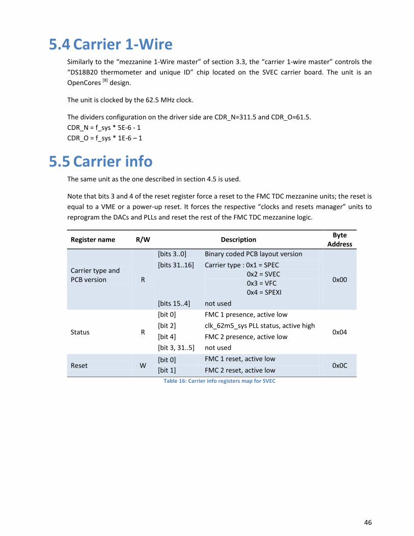
5.4 Carrier 1-Wire ................................................................................................................................ 46
5.5 Carrier info ..................................................................................................................................... 46
5.6 VIC .................................................................................................................................................. 47
5.7 Clock crossing ................................................................................................................................. 49
5.8 SVEC LEDs ....................................................................................................................................... 49
6 Source code ............................................................................................................................................ 50
7 TDC mezzanine board calibration .......................................................................................................... 51
7.1 EEPROM calibration data ............................................................................................................... 51
8 TDC application performance ................................................................................................................ 52
9 Design with White Rabbit ...................................................................................................................... 53
10 References ......................................................................................................................................... 57
4
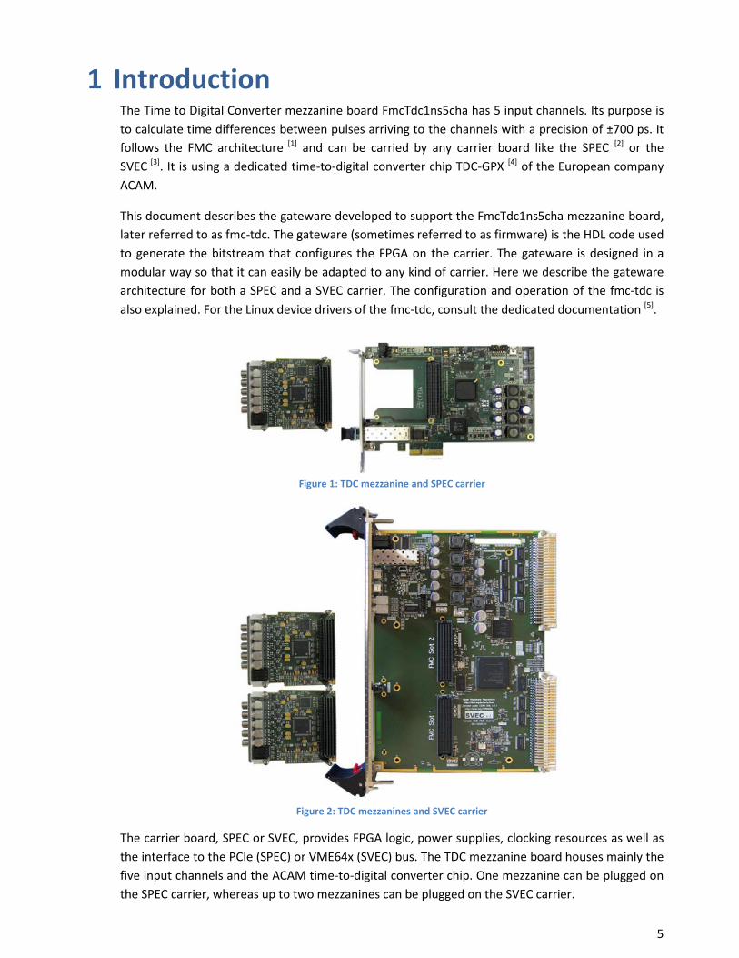
1 Introduction The Time to Digital Converter mezzanine board FmcTdc1ns5cha has 5 input channels. Its purpose is to calculate time differences between pulses arriving to the channels with a precision of ±700 ps. It follows the FMC architecture [1] and can be carried by any carrier board like the SPEC [2] or the SVEC [3]. It is using a dedicated time-to-digital converter chip TDC-GPX [4] of the European company ACAM.
This document describes the gateware developed to support the FmcTdc1ns5cha mezzanine board, later referred to as fmc-tdc. The gateware (sometimes referred to as firmware) is the HDL code used to generate the bitstream that configures the FPGA on the carrier. The gateware is designed in a modular way so that it can easily be adapted to any kind of carrier. Here we describe the gateware architecture for both a SPEC and a SVEC carrier. The configuration and operation of the fmc-tdc is also explained. For the Linux device drivers of the fmc-tdc, consult the dedicated documentation [5].
Figure 1: TDC mezzanine and SPEC carrier
Figure 2: TDC mezzanines and SVEC carrier
The carrier board, SPEC or SVEC, provides FPGA logic, power supplies, clocking resources as well as the interface to the PCIe (SPEC) or VME64x (SVEC) bus. The TDC mezzanine board houses mainly the five input channels and the ACAM time-to-digital converter chip. One mezzanine can be plugged on the SPEC carrier, whereas up to two mezzanines can be plugged on the SVEC carrier.
5
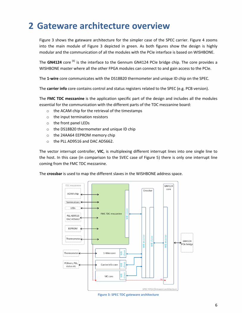
2 Gateware architecture overview Figure 3 shows the gateware architecture for the simpler case of the SPEC carrier. Figure 4 zooms into the main module of Figure 3 depicted in green. As both figures show the design is highly modular and the communication of all the modules with the PCIe interface is based on WISHBONE.
The GN4124 core [6] is the interface to the Gennum GN4124 PCIe bridge chip. The core provides a WISHBONE master where all the other FPGA modules can connect to and gain access to the PCIe.
The 1-wire core communicates with the DS18B20 thermometer and unique ID chip on the SPEC.
The carrier info core contains control and status registers related to the SPEC (e.g. PCB version).
The FMC TDC mezzanine is the application specific part of the design and includes all the modules essential for the communication with the different parts of the TDC mezzanine board:
o the ACAM chip for the retrieval of the timestamps o the input termination resistors o the front panel LEDs o the DS18B20 thermometer and unique ID chip o the 24AA64 EEPROM memory chip o the PLL AD9516 and DAC AD5662.
The vector interrupt controller, VIC, is multiplexing different interrupt lines into one single line to the host. In this case (in comparison to the SVEC case of Figure 5) there is only one interrupt line coming from the FMC TDC mezzanine.
The crossbar is used to map the different slaves in the WISHBONE address space.
Figure 3: SPEC TDC gateware architecture
6

Figure 4 shows the different parts of the FMC TDC mezzanine module and their connections to the TDC mezzanine board. The heart of this module is the TDC core, depicted in pink. The TDC core is first responsible for configuring the ACAM chip. The configuration instructions are provided through the PCIe interface. Once the ACAM chip is configured, rising edges arriving to any of its channels are time-stamped. The TDC core is responsible for retrieving the timestamps; it is then putting them in a user-convenient format and finally it is making them available to the PCIe interface.
Figure 4: FMC TDC mezzanine architecture
As mentioned above, for the configuration of the TDC core as well as of the ACAM chip, dedicated registers are allocated; they are accessible through a WISHBONE interface. The timestamps that are received by the ACAM and formatted in the core are then stored in a circular buffer, that is accessible through a different WISHBONE interface. The core has also embedded an SPI master interface for the configuration of the PLL AD9516 and the DAC AD5662 on the mezzanine.
The 1-wire core communicates with the thermometer and unique ID chip located on the mezzanine.
The I2C core communicates with the 24AA64 EEPROM memory chip on the mezzanine.
The embedded interrupts controller, EIC core, gathers all the interrupts generated by the TDC core into one single interrupt request line. The result is forwarded to the Vector Interrupt Controller, VIC.
The crossbar is used to map the different slaves in the WISHBONE address space.
7

Figure 5Figure 6 shows the gateware architecture for the case of a SVEC carrier. The communication of all the modules with the VME interface is done through WISHBONE, as in the case of SPEC. Notice that the GN4121 core is replaced by the VME64x core and that two FMC TDC mezzanine modules are instantiated, one for each one of the mezzanine boards plugged on the SVEC. A small extra complication is inserted in the SVEC design, the clocks crossing core is needed because the VME core can only run up to 62.5 MHz, whereas the FMC TDC mezzanine runs at 125 MHz.
Figure 5: SVEC TDC gateware architecture
8
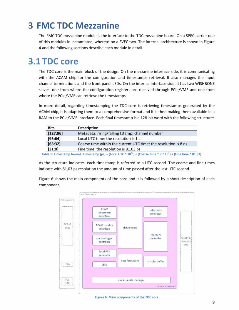
3 FMC TDC Mezzanine The FMC TDC mezzanine module is the interface to the TDC mezzanine board. On a SPEC carrier one of this modules in instantiated, whereas on a SVEC two. The internal architecture is shown in Figure 4 and the following sections describe each module in detail.
3.1 TDC core The TDC core is the main block of the design. On the mezzanine interface side, it is communicating with the ACAM chip for the configuration and timestamps retrieval. It also manages the input channel terminations and the front panel LEDs. On the internal interface side, it has two WISHBONE slaves: one from where the configuration registers are received through PCIe/VME and one from where the PCIe/VME can retrieve the timestamps.
In more detail, regarding timestamping the TDC core is retrieving timestamps generated by the ACAM chip, it is adapting them to a comprehensive format and it is then making them available in a RAM to the PCIe/VME interface. Each final timestamp is a 128-bit word with the following structure:
Bits Description [127:96] Metadata: rising/falling tstamp, channel number [95:64] Local UTC time: the resolution is 1 s [63:32] Coarse time within the current UTC time: the resolution is 8 ns [31:0] Fine time: the resolution is 81.03 ps
Table 1: Timestamp format. Timestamp [ps] = (Local UTC * 1012) + (Coarse time * 8 * 103) + (Fine time * 81.03)
As the structure indicates, each timestamp is referred to a UTC second. The coarse and fine times indicate with 81.03 ps resolution the amount of time passed after the last UTC second.
Figure 6 shows the main components of the core and it is followed by a short description of each component.
Figure 6: Main components of the TDC core
9

The “local PPS generator” unit is responsible for keeping the UTC time. The timekeeping depends on the PLL AD9516 and the DAC AD5662 on the mezzanine board, which provide a 125 MHz clock. The timebase accuracy is in the order of 4 ppm; this for example means that in 1 s there can be an error of 4’000’000 ps. Upgrades of the core with White Rabbit [7] will provide accuracy of <1 ns (see section 9).
The timestamps are formatted in the “data formatting” unit to the structure of Table 1.
Then they are stored in a RAM block implemented in the “circular buffer” unit, where the GN4124 or the VME64x core has direct access.
In this application, the ACAM is used in I-Mode [4]. This provides unlimited measuring range with internal start retriggers. ACAM's counter of retriggers however is not large enough and there is the need to follow ACAM’s retriggers inside the core; the “start retrigger control” unit is responsible for that.
The “registers controller” implements the communication with the GN4124/ VME64x core for the configuration of the TDC core and of the ACAM chip. Amongst the registers, one in particular is most important: the “control register” defines the action to be taken in the core (such as activation of timestamps acquisition, loading of configuration to the ACAM chip, etc).
The “data engine” unit is managing the state of the core according to the “control register”.
The “acam databus interface” implements the communication with the ACAM chip for its configuration as well as for the timestamps retrieval.
The “acam timecontrol interface” is responsible for delivering to the ACAM chip the start pulse, to which all timestamps are related (see section 3.1.2).
The core is providing an interrupt in any of the following three cases: o accumulation of timestamps larger than the settable threshold o more time passed than the settable time threshold and >=1 timestamps accumulated o an error occurred in the ACAM chip
The “interrupts generator” unit is responsible for generating the corresponding interrupt pulses.
The “clocks and resets manager” unit is configuring the PLL AD9516 and DAC AD5662 on the TDC mezzanine for the production of two clocks: a 125 MHz clock for the TDC core and 31.25 MHz clock for the ACAM chip. It is also managing the TDC core resets.
Finally, the “leds” unit manages the six TDC mezzanine front panel LEDs.
10
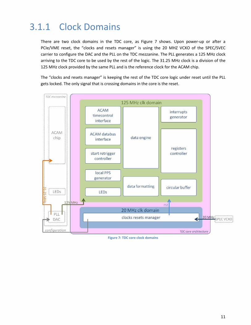
3.1.1 Clock Domains There are two clock domains in the TDC core, as Figure 7 shows. Upon power-up or after a PCIe/VME reset, the “clocks and resets manager” is using the 20 MHZ VCXO of the SPEC/SVEC carrier to configure the DAC and the PLL on the TDC mezzanine. The PLL generates a 125 MHz clock arriving to the TDC core to be used by the rest of the logic. The 31.25 MHz clock is a division of the 125 MHz clock provided by the same PLL and is the reference clock for the ACAM chip.
The “clocks and resets manager” is keeping the rest of the TDC core logic under reset until the PLL gets locked. The only signal that is crossing domains in the core is the reset.
Figure 7: TDC core clock domains
11
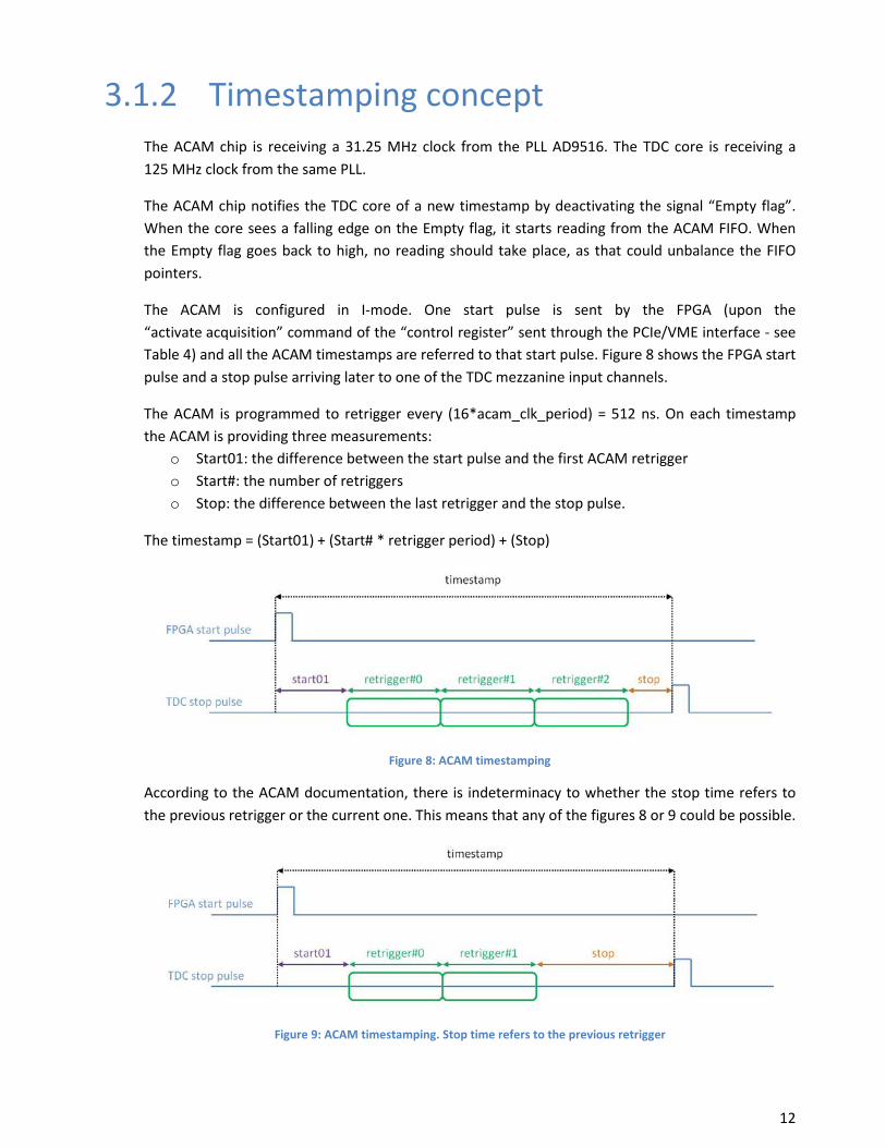
3.1.2 Timestamping concept The ACAM chip is receiving a 31.25 MHz clock from the PLL AD9516. The TDC core is receiving a 125 MHz clock from the same PLL.
The ACAM chip notifies the TDC core of a new timestamp by deactivating the signal “Empty flag”. When the core sees a falling edge on the Empty flag, it starts reading from the ACAM FIFO. When the Empty flag goes back to high, no reading should take place, as that could unbalance the FIFO pointers.
The ACAM is configured in I-mode. One start pulse is sent by the FPGA (upon the “activate acquisition” command of the “control register” sent through the PCIe/VME interface - see Table 4) and all the ACAM timestamps are referred to that start pulse. Figure 8 shows the FPGA start pulse and a stop pulse arriving later to one of the TDC mezzanine input channels.
The ACAM is programmed to retrigger every (16*acam_clk_period) = 512 ns. On each timestamp the ACAM is providing three measurements:
o Start01: the difference between the start pulse and the first ACAM retrigger o Start#: the number of retriggers o Stop: the difference between the last retrigger and the stop pulse.
The timestamp = (Start01) + (Start# * retrigger period) + (Stop)
Figure 8: ACAM timestamping
According to the ACAM documentation, there is indeterminacy to whether the stop time refers to the previous retrigger or the current one. This means that any of the figures 8 or 9 could be possible.
Figure 9: ACAM timestamping. Stop time refers to the previous retrigger
12

In this TDC application, we are only interested in differences between stop pulses, therefore the constant value “Start01” is irrelevant in the calculations. The following figure shows a simple scenario. timestamp B – timestamp A = [(Start01) + (Start#A * retrigger period) + (StopA)] - [(Start01) + (Start#B * retrigger period) + (StopB)]
Figure 10: Time difference between pulses
The counter of the ACAM chip that counts the retriggers, Start#, is restricted to 8 bits, and can only count up to 256 retriggers = 131’072 ns. Since our application needs to measure pulses separated by any amount of time, the TDC core needs to be tracking how many times the ACAM retriggers counter overflows. To do so, the ACAM Interrupt flag has been configured to follow the highest bit of the Start# counter. In the TDC core, a counter called “rollover counter” is following the Interrupt flag (Ir Flag) and is counting the overflows.
Note also that in one second, there are 7629 rollovers.
Figure 11: The TDC core is following the ACAM retriggers
In addition, the core is keeping track of the retrigger number and the number of clock cycles after the last retrigger, as Figure 11 shows.
13

As described in Table 1, each timestamp provided to the PCIe/VME interface has a UTC time component, a coarse time component and the fine time. Therefore, the ACAM retriggers have to be associated to the UTC time. The ACAM however has no knowledge of the UTC time and the arrival of a new second happens completely independently.
The “local PPS generator” unit is generating a pulse per second and is also responsible for counting the number of these pulses, keeping the UTC time. When this “local PPS pulse” arrives:
o The rollover counter is reset. o The current retrigger number is registered (retrigger#_offset). o The current number of clock cycles after the last retrigger is registered (clk#_offset).
Through the retrigger#_offset and clk#_offset the amount of time t1 can be calculated. Figure 12 shows in detail these actions.
Figure 12: Actions upon the arrival of a new "local PPS pulse"
14

Putting everything into the picture now, when a stop pulse arrives to any of the TDC channels, the ACAM chip registers the timestamp to its FIFO and puts the “Empty flag” to low. The TDC core receives the timestamp and in the “data formatting” unit it brings it into the form of Table 1. For that, as Figure 13 shows, the amounts of time t1’, t2 and t3 need to be calculated.
The amount t3 is exclusively provided by the ACAM chip in the form of Start# and Stop.
The amount t2 is the number of rollovers of the IrFlag between the last “local PPS pulse” and the Stop pulse. The rollover counter that has been reset upon the “local PPS pulse” arrival provides this amount.
The amount t1’ is the complementary of t1 and is calculated using the retrigger#_offset and the clk#_offset registered values.
This is the way the TDC core is functioning in terms of timestamps retrieval and formatting. The sections that follow describe in detail each unit of the TDC core.
Figure 13: Essential calculations to associate each timestamp to the current UTC time
Notice that the Start pulse is not in the picture and the Start01 amount of time is not used.
15

3.1.3 Clocks and Resets Manager The “clocks and resets manager” unit is responsible for providing the clocking resources to the rest of the modules. It configures the PLL AD9516 and the DAC AD5662 on the TDC mezzanine board. Upon power up or after a PCIe/VME reset, the unit is using the 20 MHz clock of the carrier board to configure the DAC and PLL through their SPI interfaces. The time needed for that is in the order of 1 ms.
The PLL is configured to provide a 125 MHz clock for the rest of the TDC core and a 31.25 MHz clock for the ACAM chip (i.e. the ACAM chip is running 4 times slower than the TDC core). The registers for the PLL configuration are hard-coded in the TDC core.
The DAC output is connected to a voltage-controlled-oscillator which in turn controls the PLL. Alterations on the DAC voltage change slightly the frequency of the pulses coming out of the PLL. Since the “local PPS generator” unit is counting seconds based on the 125 MHz of the PLL, the timestamps are affected by the DAC voltage. For example, a period of 9 ms can be measured as 8.999967000 ms with the DAC at 1.25 V and as 9.000000300 ms with the DAC at 1.65 V. During the calibration of each TDC mezzanine board, the optimal value for the DAC is measured (see section 7 on TDC calibration). The register for the DAC configuration is received through the PCIe/VME interface. Note that extension of the TDC core with White Rabbit, will relieve the design from this dependency on the local oscillator.
Figure 14: TDC clocks
The “clocks resets manager” is resetting the rest of the logic until the “PLL_lock” signal is activated. The reset pulse is synchronized to the 125 MHz domain.
16
3.1.4 Registers controller The unit interfaces with the GNUM/VME64x core for the configuration of the ACAM chip and of the TDC core. The unit implements a WISHBONE slave. All the registers are of size 32 bits, as the WISHBONE data bus.
Through WISHBONE write cycles, the unit receives: o The ACAM configuration registers. Table 2 describes the registers. o The TDC core configuration registers. Table 3 describes the registers. o The “control register” that defines the action to be taken in the core; the register is decoded
and the corresponding signals are used by the different units in the design.
Through WISHBONE read cycles, the unit transmits: o The ACAM configuration registers read back from the ACAM chip. Table 5 describes these
registers. o The TDC core status registers. These are the read-only registers in Table 3.
Table 2 lists the ACAM configuration registers and the value they should be set to through the PCIe/VME interface and WISHBONE writes. Note that the default reset value of all the registers in the FPGA is 0x0. Note that the registers are first transferred in the TDC core through PCIe/VME and then they have to be loaded to the ACAM chip. For that, the “control register” has to be properly activated (Table 4, bit 2 = ‘1’).
Refer to the ACAM documentation for a thorough description of each register [15].
ACAM Config. R/W Description Byte Address Set Value
reg. 0 R/W Timestamping of both rising and falling edges 0x000 0x01F0FC81
reg. 1 R/W Not used (channel adjustments for other modes) 0x004 0x00000000
reg. 2 R/W I-mode selection | Disabling of unused channels 0x008 0x00000E02
reg. 3 R/W Not used (resolutions and tests for other modes) 0x00C 0x00000000
reg. 4 R/W Start retriggers set to 16 | Resets 0x010 0x0200000F
reg. 5 R/W External start retrigger OFF | Offset set to 2.000 0x014 0x000007D0
reg. 6 R/W Not used for the moment (load flags) 0x018 0x00000003
reg. 7 R/W PLL values: RefClkDiv=7 | HSDiv=234 | PhaseNeg 0x01C 0x00001FEA
reg. 11 R/W Error flag configured on the 8 Hit FIFOs 0x02C 0x00FF0000
reg. 12 R/W Interrupt flag configured on the Start# overflow 0x030 0x04000000
reg. 14 R/W 16-bit mode control 0x038 0x00000000 Table 2: ACAM configuration registers
17

Table 3 lists the local configuration registers and the value they should be set to through the PCIe/VME interface and WISHBONE writes. Note that the default reset value of the registers is 0x0, apart from the IRQ tstamp thresh (reset value: 0xFF), IRQ time thresh (reset value: 0xC8) and DAC word (reset value: 0xA8F5).
Name R/W Description Byte
Address Typical
Set Value Starting UTC time R/W [bits 31..0] init value for the “local PPS generator” 0x080
Inputs enable R/W
[bit 0] input ch 1 termination enable
0x084 0x0000009F
[bit 1] input ch 2 termination enable
[bit 2] input ch 3 termination enable
[bit 3] input ch 4 termination enable
[bit 4] input ch 5 termination enable
[bit 7] general enable for all channels
[bits 5,6,31..8] not used
IRQ tstamp thresh R/W [bits 7..0]
an interrupt is issued if the number of accumulated timestamps since the last irq exceeds this threshold 0x090
0x000000FF
= full mem [bits 31..8] not used
IRQ time thresh R/W [bits 31..0] an interrupt is issued if this amount of ms has passed after the last irq and at least a timestamp has been registered
0x094 0x000000C8
= 200 ms
DAC word R/W [bits 23..0] word to be sent to the DAC
0x098 0x0000A8F5
= 1.65 V [bits 31..24] not used
Deactivate channel* R/W
[bit 0] deactivate timestamps from ch 1
0x09C 0x0
= all ch active
[bit 1] deactivate timestamps from ch 2
[bit 2] deactivate timestamps from ch 3
[bit 3] deactivate timestamps from ch 4
[bit 4] deactivate timestamps from ch 5
[bits 31..5] not used
Current UTC time R [bits 31..0] calculated by the core according to the local 125 MHz clk and the “staring utc time” register
0x0A0
Circular buffer write pointer
R [bits 11..0]
number of 8-bit-words to be read from the circular buffer = number of 128-bit-timestamps*16 0x0A8
Da Capo counter [bits 31..12] number of times the circular buffer has been overwritten
Control Register W [bits 11..0] commands the main core FSM
0x0FC See Table 4 [bits 31..12] not used
Table 3: TDC core local registers
* Note that the deactivation takes place inside the TDC core and not at the ACAM level; the ACAM continues giving all the timestamps and if a channel is deactivated (through the corresponding register bit) the received timestamps are not being registered in the circular buffer.
18

Table 4 describes the control register, which defines the state of the “data engine” state machine. Only one bit at a time can be activated since each bit is carrying a command. Upon a WISHBONE write of the control register by the PCIe/VME, a 1-tick-long control pulse is generated defining the action to be taken (eg: activate_acquisition_p, reset_acam_p, read_acam_fifo1_p); then the register is cleared.
Control Register Bit Action Description Control Register Value
Bit 0 Activate acquisition 0x00000001
Bit 1 De-activate acquisition 0x00000002
Bit 2 Load ACAM configuration registers 0x00000004
Bit 3 Read back ACAM configuration 0x00000008
Bit 4 Read ACAM status register 0x00000010
Bit 5 Read ACAM IFIFO 1 register 0x00000020
Bit 6 Read ACAM IFIFO 2 register 0x00000040
Bit 7 Read ACAM Start01 register 0x00000080
Bit 8 Reset ACAM chip 0x00000100
Bit 9 Load UTC time 0x00000200
Bit 10 Clear Write pointer and Da Capo counter 0x00000400
Bit 11 Configure DAC and reset the core 0x00000800
Bits [31 downto 12] Unused, ignored on read
Table 4: The bits of the control Register
Table 5 describes the registers read back from the ACAM chip. These are read-only registers. To initiate a reading of this set of registers, the “control register” bit 3 needs to be activated. Note that this set of registers includes the configuration registers listed in Table 2 (the values now represent what is read from the ACAM rather than what is being set through PCIe/VME) plus the ACAM Read-only registers Start01 and Interface FIFOs.
ACAM Config.
Read-back R/W Description
Byte Address
Typical Value
reg. 0 R Timestamping of both rising and falling edges 0x040 0xC1F0FC81
reg. 1 R Not used (channel adjustments for other modes) 0x044 0xC0000000
reg. 2 R I-mode selection | Disabling of unused channels 0x048 0xC0000E02
reg. 3 R Not used (resolutions and tests for other modes) 0x04C 0xC0000000
reg. 4 R Start retriggers set to 16 | Resets 0x050 0xC200000F
reg. 5 R External start retrigger OFF | Offset set to 2.000 0x054 0xC00007D0
reg. 6 R Load flag levels at maximum 0x058 0xC00000FC
reg. 7 R PLL values: RefClkDiv=7 | HSDiv=234 | PhaseNeg 0x05C 0xC0001FEA
reg. 8 R Interface FIFO 1 0x060 Start# and Stop
reg. 9 R Interface FIFO 2 0x064 Start# and Stop
reg. 10 R Start01 0x068 Start01
reg. 11 R Error flag configured on the 8 Hit FIFOs 0x06C 0xC0FF0000
reg. 12 R Interrupt flag configured on the Start# overflow 0x070 0xC4000000
reg. 14 R 16-bit mode control 0x078 0xC0000000 Table 5: ACAM read-back registers
19
3.1.5 Data Engine According to the value of the “control register” and the generated control pulses, the “data engine” unit is managing:
o The writing of the ACAM configuration. o The reading back of the ACAM configuration/status registers. o The timestamps' acquisition from the ACAM.
Figure 15 shows the states structure of the state machine. The default state is “inactive”.
From the “inactive” state the FSM jumps to “load ACAM configuration” upon the activation of the “control register” bit 3. In this state, the whole set of registers described in Table 2 are transferred one by one to the ACAM chip. The “data engine” is providing the values of the registers (as received by the PCIe/VME interface in the “registers controller” unit) and the addresses to the “acam databus interface” unit that is actually implementing the interface with the ACAM chip. Figure 16 shows the flow of actions for one register. When all the eleven registers have been transferred, the FSM jumps back to the “inactive” state. Note that all the configuration registers need to be loaded (through PCIe/VME) before setting the “control register”, otherwise the ACAM will be wrongly configured.
Similarly, the “read back ACAM configuration” state initiates readings of the set of registers described in Table 5. When all the fourteen registers have been read, the FMS goes back to the “inactive” state
Figure 15: Data engine main FSM
20
Each of the states “read ACAM FIFO1 register”, “read ACAM FIFO2 register” and “read ACAM Start01 register” initiates a single reading of the corresponding register (read-back reg 8, 9 and 10 respectively. See Table 5).
Finally the state “reset ACAM” initiates the writing of a particular word to the ACAM configuration register 4 (see Table 2) that resets the chip.
Figure 16: Snapshot of the transfer of one configuration register to the ACAM chip
21

In acquisition mode (“control register” bit 0 = ‘1’) the unit monitors permanently the ACAM Empty flags (ef1, ef2) and retrieves the timestamps by reading the ACAM read-only registers 8 or 9 (see Table 5). As described in Section 2, the register Start01 is not read. The timestamps are received by the “data formatting” unit for the formatting and are finally stored in the “circular buffer”. Figure 17 shows the sequence of events upon the Empty flag deactivation.
The maximum speed with which the ACAM can be retrieving timestamps is 31.25 MHz. If the ACAM is receiving more timestamps than that, then the ACAM Error flag is raised and the TDC core is issuing an interrupt. For the TDC core to be able to keep up with the maximum speed of 31.25 MHz (so that no timespamp gets lost by the core) it has to retrieve, format and store a timestamp within 4 cycles of the 125 MHz clock (4 * 31.25 = 125!).
Figure 17: Snapshot of the transfer of a timestamp from the ACAM to the circular buffer. The numbers below the arrows
indicate the sequence of events.
To pass from the inactive state to the active one, the “data engine” unit needs to pass from a wait state. When the software activates the acquisition the “acam timecontrol interface” unit waits unit the next UTC pulse to send the ACAM start pulse. The “data engine” should therefore only start following the ACAM empty flags after the start pulse has been sent to the ACAM, which could take up to 1 second after the activation of the acquisition.
On top, some extra time needs to be added after the delivery of the start pulse; it is the time the ACAM needs to toggle the Interrupt flag. Otherwise the offsets described in the “start retrigger controller” unit do not have meaningful values. In total the TDC operator is informed that timestamps are being registered <2 sec after the activation of the acquisition.
22

3.1.6 ACAM databus interface The unit interfaces with the ACAM chip pins for the configuration of the registers and the acquisition of the timestamps. The ACAM proprietary interface is converted to a WISHBONE classic interface, with which the unit communicates with the “data engine” unit. The WISHBONE master is implemented in the “data engine” and the slave in the “acam databus interface” unit.
Note that the TDC mezzanine board has 5 input channels. The ACAM chip is treating channels 1 to 4 in the FIFO1 and channel 5 in the FIFO2.
Figure 18: Interfaces between the "data engine", "ACM databus interface" units and the ACAM chip
Here is the description of the ACAM proprietary interface for a read operation:
Figure 19: The ACAM proprietary interface
23
Special attention needs to be paid on the ACAM Empty Flag maximum set time of Figure 19. A violation of this time, by initiating a new reading before the Empty Flag has been updated, could translate to reading from an empty FIFO and would unbalance the ACAM FIFO pointers.
In order for the “ACAM databus interface” unit to be able to keep retrieving timestamps from the ACAM at the ACAM's maximum speed (31.25 M timestamps/ sec), it needs to complete one retrieval per 4 * clk cycles = 4 * 8 ns = 32 ns. To achieve that, it is allowing 16 ns from the moment it activates the RDN until it checks the ACAM Empty flag signal and decides whether to continue reading or not. ACAM's specification defines that the maximum Empty flag set time is 11.8 ns; this allows for >4 ns for the signals routing. To make sure this constraint is met, the Xilinx design map option "Pack IO Registers/Lathes into IOBs" should be enabled.
3.1.7 Circular buffer The unit implements a Dual port RAM. Port A is attached to the WISHBONE interface where the “data formatting” unit is writing timestamps. Port B is connected to the WISHBONE master of the GN4124/VME64x core. The “data formatting” unit is only writing in the RAM and the GN4124/VME64x core is only reading from it.
The “data formatting” unit is writing timestamps of size 128 bits each (see Table 1). From port A the memory is of size: 256 * 128 bits. The GN4124/VME64x core is reading 32-bit words. Readings take place using pipelined WISHBONE interface. From this side the memory is of size: 1024 * 32.
Figure 20: The circular buffer
The GN4124/VME64x core is reading words of 32-bits, but the addressing is per byte. This is why the “write pointer” register (Table 3) is providing the number of bytes to be read, rather than the number of timestamps (=number of timestamps*16).
3.1.8 Local PPS Generator The unit implements two counters. The first one counts seconds using the 125 MHz clock. When a second has passed a 1-tick-long pulse is generated. The second counter is used to count the amount of those 1-tick-long pulses. The initial value of the last counter is zero, after a reset or after power-up. A different initial value can be given through the PCIe/VME register “starting utc time”.
Finally, the current value of the counter can be read back through the PCIe/VME register “local utc time”.
24
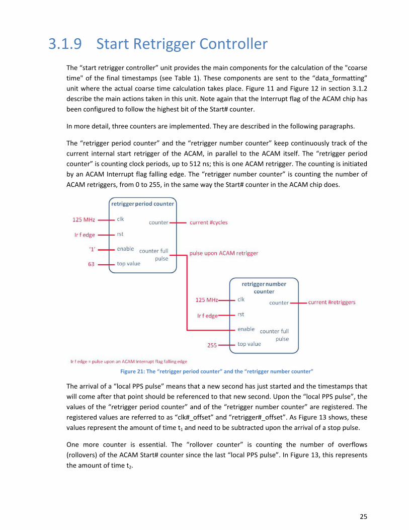
3.1.9 Start Retrigger Controller The “start retrigger controller” unit provides the main components for the calculation of the "coarse time" of the final timestamps (see Table 1). These components are sent to the “data_formatting” unit where the actual coarse time calculation takes place. Figure 11 and Figure 12 in section 3.1.2 describe the main actions taken in this unit. Note again that the Interrupt flag of the ACAM chip has been configured to follow the highest bit of the Start# counter.
In more detail, three counters are implemented. They are described in the following paragraphs.
The “retrigger period counter” and the “retrigger number counter” keep continuously track of the current internal start retrigger of the ACAM, in parallel to the ACAM itself. The “retrigger period counter” is counting clock periods, up to 512 ns; this is one ACAM retrigger. The counting is initiated by an ACAM Interrupt flag falling edge. The “retrigger number counter” is counting the number of ACAM retriggers, from 0 to 255, in the same way the Start# counter in the ACAM chip does.
Figure 21: The “retrigger period counter” and the “retrigger number counter”
The arrival of a “local PPS pulse” means that a new second has just started and the timestamps that will come after that point should be referenced to that new second. Upon the “local PPS pulse”, the values of the “retrigger period counter” and of the “retrigger number counter” are registered. The registered values are referred to as “clk#_offset” and “retrigger#_offset”. As Figure 13 shows, these values represent the amount of time t1 and need to be subtracted upon the arrival of a stop pulse.
One more counter is essential. The “rollover counter” is counting the number of overflows (rollovers) of the ACAM Start# counter since the last “local PPS pulse”. In Figure 13, this represents the amount of time t2.
25

Figure 22: The “rollover counter”
Upon the arrival of a timestamp, the “data formatting” unit is using the “clk#_offset”, “retrigger#_offset” and the current value of the “rollover counter” for the calculations of the values to be used to arrive to a timestamp related to the current second.
26

3.1.10 Data Formatting The “data formatting” unit brings the ACAM timestamps to the format of Table 1. It also writes them to the “circular buffer” unit, according to the value of the “deactivate channel” register (see Table 3); if a bit of the “deactivate channel” register is enabled, timestamps from the corresponding channel are not written in the buffer. The unit is also responsible for keeping track of how many timestamps have been written.
When a timestamp arrives the UTC time, coarse time and fine time need to be calculated.
The UTC time comes directly from the “local PPS generator” unit. The timestamp will be referenced to the last UTC second.
The fine time comes directly from the Stop value of the ACAM timestamp (Figure 8).
Now, for the coarse time, i.e. amount of 8 ns cycles between the last “local PPS pulse” and the timestamp, the following calculations need to take place.
o The “roll over counter” has been counting the multiples of 256 retriggers since the last “local PPS pulse” (i.e. number of pink boxes in Figure 23).
o The “retrigger#_offset” has kept the amount of retriggers that had preceded the arrival of the “local PPS pulse” (ie. number of green boxes inside the first pink box in Figure 23).
o The ACAM Start# indicates the amount of retriggers within the last pink box of Figure 23.
Therefore, the number of retriggers is defined by the following equation [I]:
“#retriggers” = “current value of the rollover counter”*256 + “Start#” – “retrigger#_offset” [I]
Now we need to translate this number of retriggers to the amount of 8 ns cycles. The ACAM is configured to retrigger each 512 ns.
Therefore “#cycles from retriggers” = “#retriggers” * 64.
Figure 23: Data formatting calculations. Same as Figure 13
27
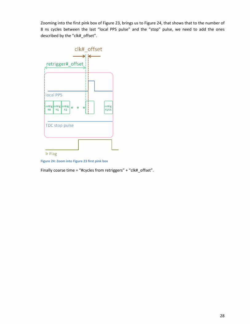
Zooming into the first pink box of Figure 23, brings us to Figure 24, that shows that to the number of 8 ns cycles between the last “local PPS pulse” and the “stop” pulse, we need to add the ones described by the “clk#_offset”.
Figure 24: Zoom into Figure 23 first pink box
Finally coarse time = “#cycles from retriggers” + “clk#_offset”.
28

Unfortunately, there are three exceptions to the calculation above.
The first exception comes from the marginal case where the “local PPS pulse” and the “stop” pulse arrive within the same retrigger. In this case equation [I] equals to zero! The “current value of the rollover counter” is zero and both the ACAM and the TDC core are at the same retrigger number.
Figure 25: Marginal case where the “local PPS pulse” and the “stop” pulse arrive within the same retrigger
For this case, the timestamp needs to be referenced to the previous second. As Figure 26 shows, the pulse is referenced to the previous “local PPS pulse” and the amount of time t3 is provided exclusively by the ACAM.
Figure 26: Calculations on the marginal case where the “local PPS pulse” and the “stop” pulse arrive within the same
retrigger
29

Attention though needs to be put in the case described in Figure 9 where the fine time refers to the previous retrigger rather than the current one. In this case:
o “current value of the rollover counter” = 0 o “Start#” = “retrigger#_offset” - 1 o ACAM “Stop” is > 6318 (6318 * 81 ps = 512 ns)
If all the conditions above are valid, it means, exactly as described before, that that the last “local PPS pulse” and the “stop” pulse have arrived within the same retrigger. In this case again, as Figure 26 shows the timestamp is referenced to the to the previous “local PPS pulse”.
The last exception comes from the marginal case where a timestamp is received from the ACAM when the “rollover counter” has just been increased. In this case, it is possible that the timestamp belongs to the previous roll-over value. This is because the moment the ACAM IrFlag is taken into account in the TDC core is different from the moment the “stop” pulse has arrived to the ACAM (several 8 ns cycles are needed to empty ACAM FIFOs). In this case if the ACAM “Start#” of the received timestamp is close to the upper end (close to 255) and on the moment of processing in the
“data formatting” unit the IrFlag has recently increased, that means that in equation [I], the “current value of the rollover counter” - 1 needs to be used.
30
3.1.11 Interrupts generator The “interrupts generator” is responsible for the generation of 1-tick-long pulses in any of the following three cases:
o when the amount of timestamps written in the “circular_buffer”, since the last interrupt or since the startup of the acquisition, exceeds the PCIe/VME settable threshold irq_tstamp_threshold. We refer to this interrupt as “timestamps interrupt”.
o when some timestamps have been written in the circular_buffer (>=1 timestamp) and the amount of time passed since the last interrupt or since the acquisition startup, exceeds the PCIe/VME settable threshold irq_time_threshold. We refer to this interrupt as “time interrupt”.
o when the ACAM raises the Error flag; this means that the ACAM Hit FIFOs have been receiving pulses with a frequency > 31.25 MHz. We refer to this interrupt as “acam error interrupt”.
The pulses are retrieved by the “tdc eic” core (see Figure 4) which gathers them into a single line.
3.1.12 ACAM timecontrol interface Upon the activation of the acquisition through the “control register” bit 0 (see Table 4), the unit generates a 16 ns long pulse, synchronous to the “local PPS pulse” that represents the ACAM start pulse (see Figure 8).
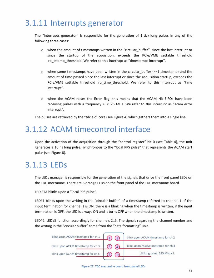
3.1.13 LEDs The LEDs manager is responsible for the generation of the signals that drive the front panel LEDs on the TDC mezzanine. There are 6 orange LEDs on the front panel of the TDC mezzanine board.
LED STA blinks upon a “local PPS pulse”.
LED#1 blinks upon the writing in the “circular buffer” of a timestamp referred to channel 1. If the input termination for channel 1 is ON, there is a blinking when the timestamp is written; if the input termination is OFF, the LED is always ON and it turns OFF when the timestamp is written.
LED#2..LED#5 function accordingly for channels 2..5. The signals regarding the channel number and the writing in the “circular buffer” come from the “data formatting” unit.
Figure 27: TDC mezzanine board front panel LEDs
31
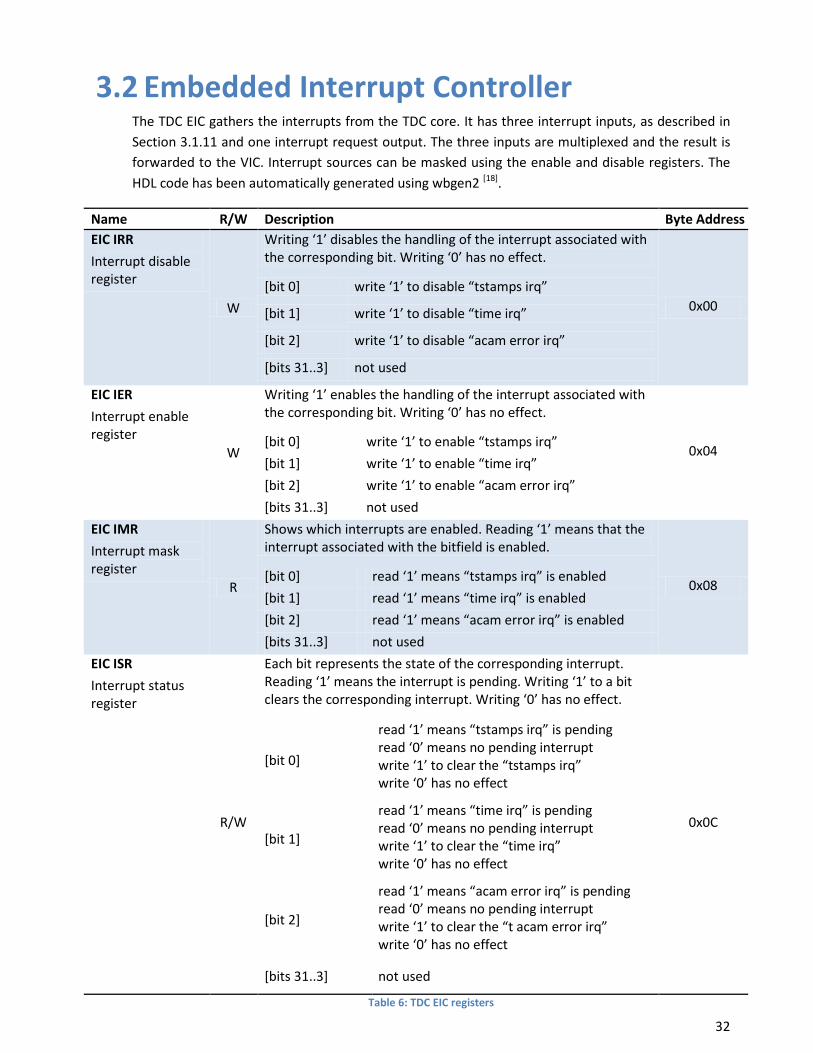
3.2 Embedded Interrupt Controller The TDC EIC gathers the interrupts from the TDC core. It has three interrupt inputs, as described in Section 3.1.11 and one interrupt request output. The three inputs are multiplexed and the result is forwarded to the VIC. Interrupt sources can be masked using the enable and disable registers. The HDL code has been automatically generated using wbgen2 [18].
Name R/W Description Byte Address EIC IRR
Interrupt disable register
W
Writing ‘1’ disables the handling of the interrupt associated with the corresponding bit. Writing ‘0’ has no effect.
0x00 [bit 0] write ‘1’ to disable “tstamps irq”
[bit 1] write ‘1’ to disable “time irq”
[bit 2] write ‘1’ to disable “acam error irq”
[bits 31..3] not used
EIC IER
Interrupt enable register
W
Writing ‘1’ enables the handling of the interrupt associated with the corresponding bit. Writing ‘0’ has no effect.
0x04 [bit 0] write ‘1’ to enable “tstamps irq”
[bit 1] write ‘1’ to enable “time irq”
[bit 2] write ‘1’ to enable “acam error irq”
[bits 31..3] not used
EIC IMR
Interrupt mask register
R
Shows which interrupts are enabled. Reading ‘1’ means that the interrupt associated with the bitfield is enabled.
0x08 [bit 0] read ‘1’ means “tstamps irq” is enabled
[bit 1] read ‘1’ means “time irq” is enabled
[bit 2] read ‘1’ means “acam error irq” is enabled
[bits 31..3] not used
EIC ISR
Interrupt status register
R/W
Each bit represents the state of the corresponding interrupt. Reading ‘1’ means the interrupt is pending. Writing ‘1’ to a bit clears the corresponding interrupt. Writing ‘0’ has no effect.
0x0C
[bit 0]
read ‘1’ means “tstamps irq” is pending read ‘0’ means no pending interrupt write ‘1’ to clear the “tstamps irq” write ‘0’ has no effect
[bit 1]
read ‘1’ means “time irq” is pending read ‘0’ means no pending interrupt write ‘1’ to clear the “time irq” write ‘0’ has no effect
[bit 2]
read ‘1’ means “acam error irq” is pending read ‘0’ means no pending interrupt write ‘1’ to clear the “t acam error irq” write ‘0’ has no effect
[bits 31..3] not used
Table 6: TDC EIC registers
32

3.3 1-Wire The 1-Wire master controls the “DS18B20 thermometer and unique ID” chip located on the mezzanine board. The unit is an OpenCores design [8].
The unit is clocked by the 125 MHz clock.
The dividers configuration are CDR_N=624 and CDR_O=124. CDR_N = f_sys * 5E-6 - 1 CDR_O = f_sys * 1E-6 - 1
3.4 I2C The I2C master accesses the 24AA64 64Kb EEPROM memory chip [9] located on the mezzanine board. This memory is mandatory as specified in the FMC standard (VITA 57.1). It is connected to the system management I2C bus, also specified in the FMC standard. The unit is an OpenCores design [10].
The unit is clocked by the 125 MHz clock. For a SCL clock of 100 kHz, the prescaler configuration is PRESCALER=249. PRESCALER = f_sys / (5 * f_scl) – 1
The I2C slave address is 0x50.
3.5 Crossbar The crossbar is used to map the different slaves in the WISHBONE address space. It also implements SDB records [11]. The unit is part of the general-cores library [12].
The SDB records describe the WISHBONE slaves and their mapping to the bus. The SDB records ROM is located at address 0x0.
Byte Address WISHBONE slave 0x00000 Crossbar SDB records 0x10000 1-Wire 0x11000 TDC configuration 0x12000 EIC 0x13000 I2C 0x14000 TDC memory for timestamps retrieval
Table 7: FMC TDC mezzanine WISHBONE bus memory mapping
33
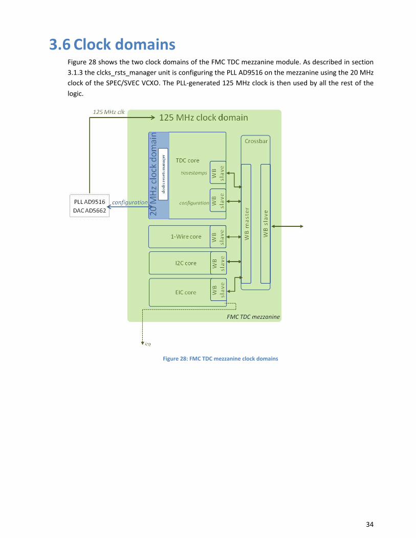
3.6 Clock domains Figure 28 shows the two clock domains of the FMC TDC mezzanine module. As described in section 3.1.3 the clcks_rsts_manager unit is configuring the PLL AD9516 on the mezzanine using the 20 MHz clock of the SPEC/SVEC VCXO. The PLL-generated 125 MHz clock is then used by all the rest of the logic.
Figure 28: FMC TDC mezzanine clock domains
34

4 SPEC TDC Figure 29 shows the gateware architecture on a SPEC carrier. All the blocks are connected to the PCIe interface using the same WISHBONE bus.
Six components are instantiated:
o The FMC TDC mezzanine, as described thoroughly in section 3. o The crossbar is used to map the different slaves in the WISHBONE address space. o The GN4124 core is the interface to the Gennum GN4124 PCIe bridge chip. o The 1-wire core communicates with the DS18B20 thermometer and unique ID chip on the
SPEC. o The carrier info core contains control and status registers related to the SPEC. o The VIC is handling the interrupts.
The following sections describe the different modules.
Figure 29: SPEC TDC gateware architecture (same as Figure 1)
35
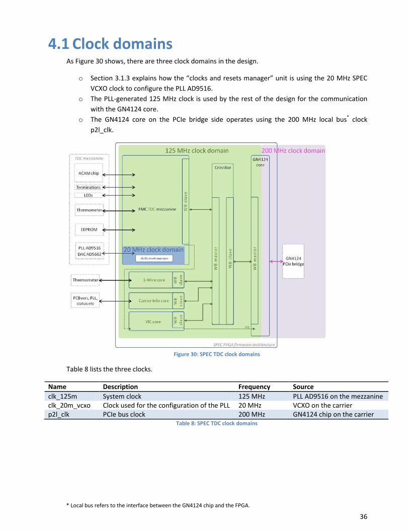
4.1 Clock domains As Figure 30 shows, there are three clock domains in the design.
o Section 3.1.3 explains how the “clocks and resets manager” unit is using the 20 MHz SPEC VCXO clock to configure the PLL AD9516.
o The PLL-generated 125 MHz clock is used by the rest of the design for the communication with the GN4124 core.
o The GN4124 core on the PCIe bridge side operates using the 200 MHz local bus* clock p2l_clk.
Figure 30: SPEC TDC clock domains
Table 8 lists the three clocks.
Name Description Frequency Source clk_125m System clock 125 MHz PLL AD9516 on the mezzanine clk_20m_vcxo Clock used for the configuration of the PLL 20 MHz VCXO on the carrier p2l_clk PCIe bus clock 200 MHz GN4124 chip on the carrier
Table 8: SPEC TDC clock domains
* Local bus refers to the interface between the GN4124 chip and the FPGA.
36

4.2 GN4124 core This block is the interface between the GN41245 local bus and the other blocks in the FPGA.
The GN4124 chip [6] is a four lane PCI Express Generation 1.1 bridge. In addition to the PHY, it contains the data link and transaction layers. The GN4124 bridge is used to access the FPGA registers, but also to generate MSI interrupts and re-program the FPGA.
The BAR 4 (Base Address Register) allows access to the GN4124 chip internal registers. The BAR 0 is connected to the local bus and therefore allows access to the FPGA.
The GN4124 core is made of a local bus interface with the GN4124 chip, a WISHBONE bus master mapped to BAR0 and a DMA controller. The TDC design is not making use of the DMA, it is only using the classic WISHBONE bus. The GN4124 core WISHBONE interfaces (masters and slave) are 32-bit data width and 32-bit word aligned addresses.
37

4.3 Crossbar The crossbar is used to map the different slaves in the WISHBONE address space. Table 9 shows the WISHBONE slaves mapping and hierarchy. The first column represents the byte address offset from the start of the WISHBONE address space (BAR 0).
Byte Address WISHBONE slave 0x00000 Crossbar SDB records 0x10000 Carrier 1-Wire 0x20000 Carrier info 0x30000 VIC 0x40000 Bridge FMC TDC mezzanine (Crossbar SDB records) 0x50000 1-Wire 0x51000 TDC configuration 0x52000 EIC 0x53000 I2C 0x54000 TDC memory for timestamps retrieval
Table 9: WISHBONE bus memory mapping (BAR 0)
In order to identify the gateware, the crossbar includes tow SDB meta-information records: “synthesis information” and “repository url”. Table 10 describes the different fields of each record.
SDB record
Fields Field content Description
Repo url repo_url "http://svn.ohwr.org/fmc-tdc " string, 63 char
Synthesis
syn_module_name "spec_tdc " string, 16 char syn_commit_id syn_tool_name "ISE " string 8 char syn_tool_version 0x00000134 bcd encoded, 32 bits syn_date 0x20140617 bcd encoded, 32 bits syn_username "egousiou " string, 15 char
Table 10: SDB meta-information records
38
4.4 Carrier 1-Wire Similarly to the “mezzanine 1-Wire master” of section 3.3, the “carrier 1-wire master” controls the “DS18B20 thermometer and unique ID” chip located on the SPEC carrier board. The unit is an OpenCores [8] design.
The unit is clocked by the 125 MHz clock.
The dividers configuration are CDR_N=624 and CDR_O=124. CDR_N = f_sys * 5E-6 - 1 CDR_O = f_sys * 1E-6 – 1
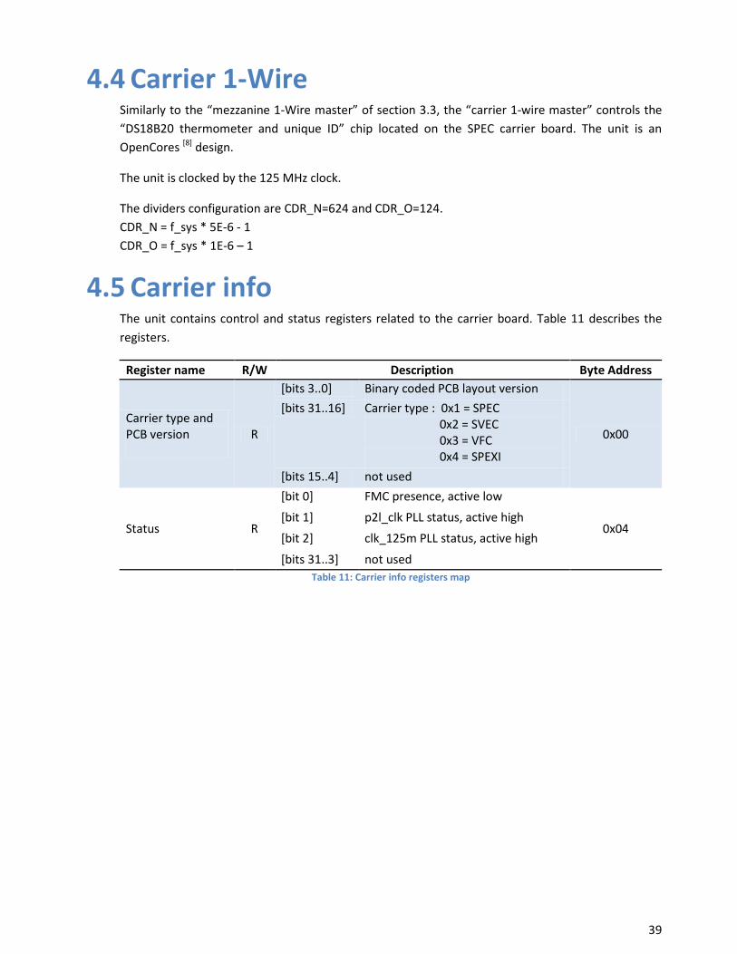
4.5 Carrier info The unit contains control and status registers related to the carrier board. Table 11 describes the registers.
Register name R/W Description Byte Address
Carrier type and PCB version
R
[bits 3..0] Binary coded PCB layout version
0x00
[bits 31..16] Carrier type : 0x1 = SPEC 0x2 = SVEC 0x3 = VFC 0x4 = SPEXI
[bits 15..4] not used
Status R
[bit 0] FMC presence, active low
0x04 [bit 1] p2l_clk PLL status, active high
[bit 2] clk_125m PLL status, active high
[bits 31..3] not used Table 11: Carrier info registers map
39

4.6 VIC In order to redirect interrupts from different cores to the corresponding driver in the Linux kernel in a generic way, a two layers scheme is used. The first layer is the Embedded Interrupt Controllers, explained in section 3.2, which is multiplexing the different interrupt sources of the FMC TDC mezzanine module into one single line. The second layer is the Vectored Interrupt Controller, VIC, which is multiplexing interrupt lines from different EICs into a single line to the host. On the SPEC carrier, the VIC interrupt request output is connected to the GPIO 8 of the GN4124 chip. Therefore, the GN4124 must be configured to generate a MSI when a rising edge is detected on GPIO 8.
The VIC keeps a table (IVT_RAM) initialized with the base addresses of the EICs connected to each one of its inputs. Here there is only the FMC TDC EIC at address 0x52000. Table 12 describes all the VIC registers.
Register name R/W Description Byte
Address
CTL VIC Control reg
R/W
[bit 0] ENABLE Write ‘1’ to enable the VIC operation Write ‘0’ to disable the VIC operation
0x00
[bit 1] POL Write ‘1’ to set the IRQ output active high Write ‘0’ to set the IRQ output active low
[bit 2] EMU_ EDGE
Write ‘1’ to force a low pulse of EMU_LEN--clock-cycles at each write to EOIR. Write ‘0’ for a normal IQR master line behavior
[bit 3] EMU_ LEN
Length of the delay between write to EOIR and re-assertion of irq_master_o
RISR Raw Irq Status
R [bit 0] Current state of the FMC TDC mezzanine interrupt
0x04 [bits 31..1] Not used
IER Irq Enable Reg
W [bit 0]
Write ‘1’ to enable the FMC TDC mezzanine interrupt Write ‘0’ has no effect 0x08
[bits 31..1] Not used
IDR Irq Disable Reg
W [bit 0]
Write ‘1’ to disable the FMC TDC mezzanine interrupt Write ‘0’ has no effect 0x0C
[bits 31..1] Not used
IMR Irq Mask
R [bit 0]
Read ‘1’ means FMC TDC mezzanine interrupt is enabled Read ‘0’ means FMC TDC mezzanine interrupt is disabled 0x10
[bits 31..1] Not used
VAR Vector Address reg
R [bits 31..0] Address of the pending interrupt vector, read from the IVT_RAM 0x14
SWIR Software Irq Reg
W [bits 31..0] Writing ‘1’ to one of the bits causes a software emulation of the respective interrupt. 0x18
EOIR End Of Irq Ack Reg
W [bit 0]
Writing ‘1’ acknowledges an FMC TDC mezzanine pending interrupt 0x1C
[bits 31..1] Not used
MEM RAM with Interrupt Vector Table
R [bits 31..0]
IVT_RAM
Contain the address “0x52000” of the FMC TDC mezzanine EIC WISHBONE slave 0x20
Rest of the RAM not used 0x24.. 0x3F
Table 12: VIC register map
40

As the GN4124 chip is an edge-only IRQ controller, an edge sensitive configuration should be used by the drivers, with the following characteristics:
VIC control register ENABLE = ‘1’ POL = ‘1’ EMU_EDGE = ‘1’ EMU_LEN = 750 IER(0) = ‘1’
Table 13: VIC configuration for SPEC
41

5 SVEC TDC Figure 31 shows the gateware architecture on a SVEC carrier. All the blocks are connected to the VME interface using the same WISHBONE bus.
The design is composed of:
o Tow FMC TDC mezzanines, as described thoroughly in section 3. o The crossbar is used to map the different slaves in the WISHBONE address space. o The VME64x core is the interface to the VME bus. o The 1-wire core communicates with the SVEC DS18B20 thermometer and unique ID chip. o The carrier info core contains control and status registers related to the SVEC. o The VIC is handling the interrupts. o The clock_crossing cores are used to pass the signals from the 125 MHz clock domains of
the FMC TDC mezzanines to the 62.5 MHz domain that the VME core functions.
Figure 31: SVEC TDC gateware architecture (same as Figure 5)
42
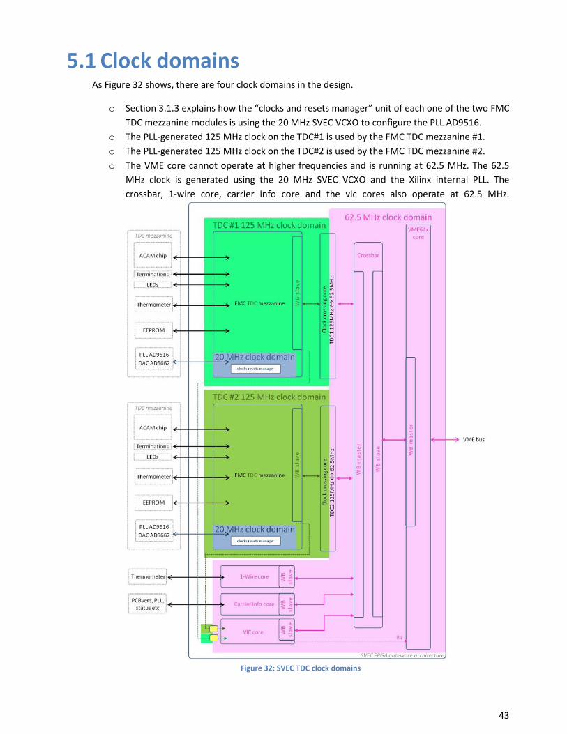
5.1 Clock domains As Figure 32 shows, there are four clock domains in the design.
o Section 3.1.3 explains how the “clocks and resets manager” unit of each one of the two FMC TDC mezzanine modules is using the 20 MHz SVEC VCXO to configure the PLL AD9516.
o The PLL-generated 125 MHz clock on the TDC#1 is used by the FMC TDC mezzanine #1. o The PLL-generated 125 MHz clock on the TDC#2 is used by the FMC TDC mezzanine #2. o The VME core cannot operate at higher frequencies and is running at 62.5 MHz. The 62.5
MHz clock is generated using the 20 MHz SVEC VCXO and the Xilinx internal PLL. The crossbar, 1-wire core, carrier info core and the vic cores also operate at 62.5 MHz.
Figure 32: SVEC TDC clock domains
43

Table 14 lists the four clocks.
Name Description Frequency Source
clk_20m_vcxo
Clock used for the configuration of the PLLs on the two TDC mezzanines. Also used for the generation of the 62.5 MHz clock by the Xilinx internal PLL.
20 MHz VCXO on the carrier
tdc1_clk_125m FMC TDC mezzanine #1 clock 125 MHz PLL AD9516 on TDC#1 tdc2_clk_125m FMC TDC mezzanine #2 clock 125 MHz PLL AD9516 on TDC#2
clk_62m5_sys System clock 62.5 MHz VCXO on the carrier and Xilinx PLL
Table 14: SPEC TDC clock domains
44

5.2 VME64x core The VME64x core implements a VME slave on one side and a WISHBONE pipelined master on the other side. For more information about the VME64x core, visit the OHWR page [13].
5.3 Crossbar The crossbar is used to map the different slaves in the WISHBONE address space. Table 15 shows the WISHBONE slaves mapping and hierarchy. The first column represents the byte address offset from the start of the WISHBONE address space.
Byte Address WISHBONE slave 0x00000 Crossbar SDB records 0x10000 Carrier 1-Wire 0x20000 Carrier info 0x30000 VIC 0x40000 Bridge FMC TDC mezzanine #1 (Crossbar SDB records) 0x50000 1-Wire 0x51000 TDC configuration 0x52000 EIC 0x53000 I2C 0x54000 TDC memory for timestamps retrieval 0x60000 Bridge FMC TDC mezzanine #2(Crossbar SDB records) 0x60000 1-Wire 0x61000 TDC configuration 0x62000 EIC 0x63000 I2C 0x64000 TDC memory for timestamps retrieval
Table 15: WISHBONE bus memory mapping for SVEC
In order to identify the gateware, the crossbar includes two SDB meta-information records: “repository url” and “synthesis information”.
SDB record
Fields Field content Description
Repo url repo_url "http://svn.ohwr.org/fmc-tdc " string, 63 char
Synthesis
syn_module_name "svec_tdc " string, 16 char syn_commit_id syn_tool_name "ISE " string 8 char syn_tool_version 0x00000134 bcd encoded, 32 bits syn_date 0x20140617 bcd encoded, 32 bits syn_username "egousiou " string, 15 char
Table 16: SDV meta-information records
45
5.4 Carrier 1-Wire Similarly to the “mezzanine 1-Wire master” of section 3.3, the “carrier 1-wire master” controls the “DS18B20 thermometer and unique ID” chip located on the SVEC carrier board. The unit is an OpenCores [8] design.
The unit is clocked by the 62.5 MHz clock.
The dividers configuration on the driver side are CDR_N=311.5 and CDR_O=61.5. CDR_N = f_sys * 5E-6 - 1 CDR_O = f_sys * 1E-6 – 1
5.5 Carrier info The same unit as the one described in section 4.5 is used.
Note that bits 3 and 4 of the reset register force a reset to the FMC TDC mezzanine units; the reset is equal to a VME or a power-up reset. It forces the respective “clocks and resets manager” units to reprogram the DACs and PLLs and reset the rest of the FMC TDC mezzanine logic.
Register name R/W Description Byte
Address
Carrier type and PCB version
R
[bits 3..0] Binary coded PCB layout version
0x00
[bits 31..16] Carrier type : 0x1 = SPEC 0x2 = SVEC 0x3 = VFC 0x4 = SPEXI
[bits 15..4] not used
Status R
[bit 0] FMC 1 presence, active low
0x04 [bit 2] clk_62m5_sys PLL status, active high
[bit 4] FMC 2 presence, active low
[bit 3, 31..5] not used
Reset W [bit 0] FMC 1 reset, active low
0x0C [bit 1] FMC 2 reset, active low
Table 16: Carrier info registers map for SVEC
46

5.6 VIC As described in section 4.6, in order to redirect interrupts from different cores to the corresponding driver in the Linux kernel in a generic way, a two layers scheme is used. The first layer is the Embedded Interrupt Controllers, explained in section 3.2, which is multiplexing the different interrupt sources of the FMC TDC mezzanine module into one single line. The second layer is the Vectored Interrupt Controller, VIC, which is multiplexing interrupt lines from different EICs into a single line to the host.
The VIC keeps a table (IVT_RAM) initialized with the base addresses of the EICs connected to each one of its inputs. Here the FMC TDC #1 EIC is at address 0x52000 and the FMC TDC #1 EIC at address 0x62000. Table 18 describes all the VIC registers.
47
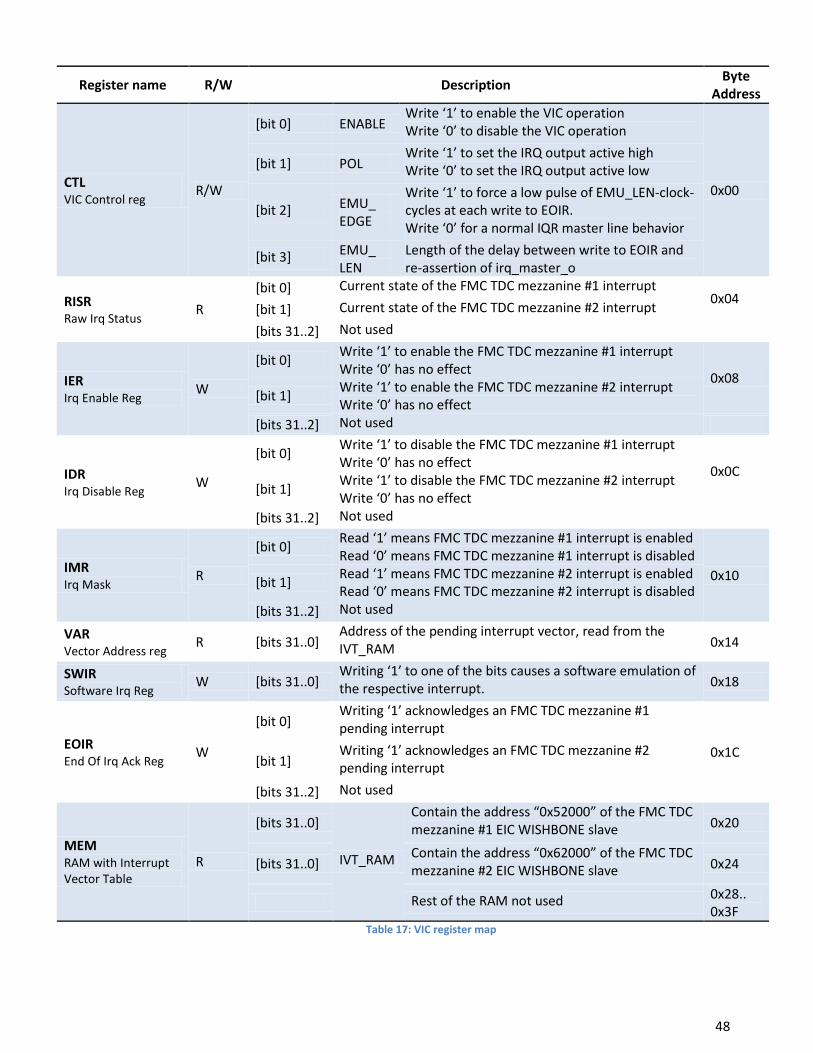
Register name R/W Description Byte
Address
CTL VIC Control reg
R/W
[bit 0] ENABLE Write ‘1’ to enable the VIC operation Write ‘0’ to disable the VIC operation
0x00
[bit 1] POL Write ‘1’ to set the IRQ output active high Write ‘0’ to set the IRQ output active low
[bit 2] EMU_ EDGE
Write ‘1’ to force a low pulse of EMU_LEN-clock- cycles at each write to EOIR. Write ‘0’ for a normal IQR master line behavior
[bit 3] EMU_ LEN
Length of the delay between write to EOIR and re-assertion of irq_master_o
RISR Raw Irq Status
R
[bit 0] Current state of the FMC TDC mezzanine #1 interrupt 0x04
[bit 1] Current state of the FMC TDC mezzanine #2 interrupt
[bits 31..2] Not used
IER Irq Enable Reg
W
[bit 0] Write ‘1’ to enable the FMC TDC mezzanine #1 interrupt Write ‘0’ has no effect
0x08 [bit 1]
Write ‘1’ to enable the FMC TDC mezzanine #2 interrupt Write ‘0’ has no effect
[bits 31..2] Not used
IDR Irq Disable Reg
W
[bit 0] Write ‘1’ to disable the FMC TDC mezzanine #1 interrupt Write ‘0’ has no effect
0x0C [bit 1]
Write ‘1’ to disable the FMC TDC mezzanine #2 interrupt Write ‘0’ has no effect
[bits 31..2] Not used
IMR Irq Mask
R
[bit 0] Read ‘1’ means FMC TDC mezzanine #1 interrupt is enabled Read ‘0’ means FMC TDC mezzanine #1 interrupt is disabled
0x10 [bit 1] Read ‘1’ means FMC TDC mezzanine #2 interrupt is enabled Read ‘0’ means FMC TDC mezzanine #2 interrupt is disabled
[bits 31..2] Not used
VAR Vector Address reg
R [bits 31..0] Address of the pending interrupt vector, read from the IVT_RAM 0x14
SWIR Software Irq Reg
W [bits 31..0] Writing ‘1’ to one of the bits causes a software emulation of the respective interrupt. 0x18
EOIR End Of Irq Ack Reg
W
[bit 0] Writing ‘1’ acknowledges an FMC TDC mezzanine #1 pending interrupt
0x1C [bit 1]
Writing ‘1’ acknowledges an FMC TDC mezzanine #2 pending interrupt
[bits 31..2] Not used
MEM RAM with Interrupt Vector Table
R
[bits 31..0]
IVT_RAM
Contain the address “0x52000” of the FMC TDC mezzanine #1 EIC WISHBONE slave 0x20
[bits 31..0] Contain the address “0x62000” of the FMC TDC mezzanine #2 EIC WISHBONE slave 0x24
Rest of the RAM not used 0x28.. 0x3F
Table 17: VIC register map
48
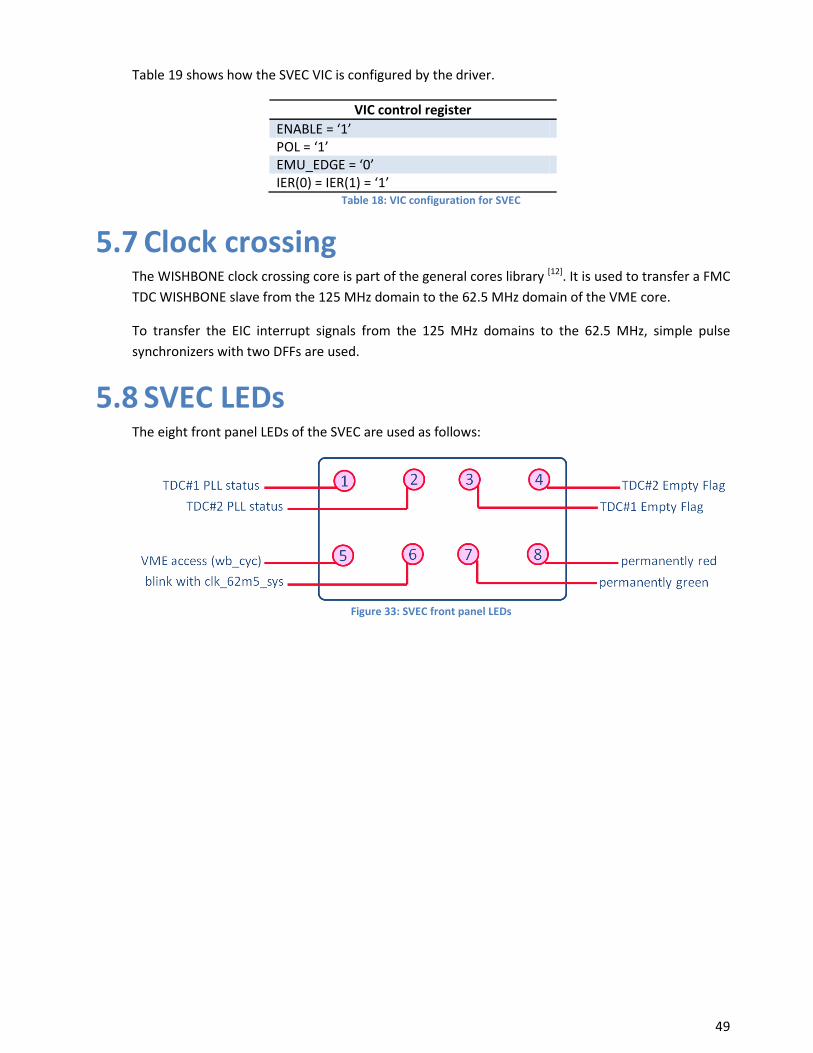
Table 19 shows how the SVEC VIC is configured by the driver.
VIC control register ENABLE = ‘1’ POL = ‘1’ EMU_EDGE = ‘0’ IER(0) = IER(1) = ‘1’
Table 18: VIC configuration for SVEC
5.7 Clock crossing The WISHBONE clock crossing core is part of the general cores library [12]. It is used to transfer a FMC TDC WISHBONE slave from the 125 MHz domain to the 62.5 MHz domain of the VME core.
To transfer the EIC interrupt signals from the 125 MHz domains to the 62.5 MHz, simple pulse synchronizers with two DFFs are used.
5.8 SVEC LEDs The eight front panel LEDs of the SVEC are used as follows:
Figure 33: SVEC front panel LEDs
49
6 Source code The TDC design is available under git in the ohwr.org repository: http://www.ohwr.org/projects/fmc-tdc-1ns-5cha-gw/repository/revisions/master/show/hdl
The source code organization is as follows:
/hdl/rtl : TDC specific HDL sources. It includes all the components of the TDC core up to the top level of the FMC TDC mezzanine.
/hdl/ip_cores: It includes modules from the general-cores library, the GN4124 and VME64x core, as well as the Xilinx block RAM for the TDC circular buffer. It also includes the White Rabbit specific modules.
/hdl/top/spec/no_wrabbit: top level HDL for a SPEC carrier without White Rabbit support.
/hdl/top/spec/with_wrabbit: top level HDL for a SPEC carrier with White Rabbit (see Section 9).
/hdl/top/svec/no_wrabbit: top level HDL for a SVEC carrier without White Rabbit support.
/hdl/top/svec/with_wrabbit: top level HDL for a SVEC carrier with White Rabbit (see Section 9).
/hdl/syn/spec/no_wrabbit: ISE project for the synthesis for a SPEC carrier without White Rabbit support. It includes map and par report of the last synthesis.
/hdl/syn/spec/with_wrabbit: ISE project for the synthesis for a SPEC carrier with White Rabbit support. It includes map and par report of the last synthesis.
/hdl/syn/svec/no_wrabbit: ISE project for the synthesis for a SVEC carrier without White Rabbit support. It includes map and par report of the last synthesis.
/hdl/syn/svec/with_wrabbit: ISE project for the synthesis for a SVEC carrier with White Rabbit support. It includes map and par report of the last synthesis.
/hdl/sim/spec: Simulation files and test benches for a SPEC carrier.
/hdl/sim/svec: Simulation files and test benches for a SVEC carrier.
To build the design from the sources the following steps are needed: 1) Download the git repository. The repository includes all the files essential for the design. 2) For a SPEC carrier: run the Xilinx ISE project located in the /hdl/syn/spec folder
For a SVEC carrier: run the Xilinx ISE project located in the /hdl/syn/svec folder The constraints for the synthesis, mapping and par-ing are included in the project. Notice the “-pr: for inputs and outputs” option in the mapping properties, as mentioned in section 3.1.6)
50
7 TDC mezzanine board calibration The TDC mezzanine board has 5 input channels. The track length from an input to the ACAM chip differs from channel to channel. In addition the input logic (clock buffers) of each channel is introducing different delays that can vary up to 2 ns. That is why it is essential to calibrate the TDC board channels. For more information, refer to the channels calibration [16] documentation.
Moreover the DAC IC2 on the board controls the OSC2 voltage-controlled-oscillator which in turn controls the PLL IC6. Alterations on the DAC voltage change slightly the frequency of the pulses coming out of the PLL and therefore the timestamp measurements. For example, the difference between two pulses separated by 9 ms can be measured as 8.999967000 ms with the DAC at 1.25 V and as 9.000000300 ms with the DAC at 1.65 V. Note also that the VCXO OSC2 is strongly influenced by temperature changes; the documentation specifies 0.5ppm/oC. For more information, refer to the DAC calibration [16] document.
The TDC-PTS-Calibration suite [17] provides the automated environment for the calibration of each board. It is using a very precise pulse generator, the Pendulum CNT-91 connected to a Cesium clock. The calibration data along with IPMI information is written in the TDC EEPROM.
7.1 EEPROM calibration data All the calibration values are stored in the TDC mezzanine EEPROM. The EEPROM holds a sdbfs [19] file system. In addition to the calibration values, the EEPROM also contains mandatory IPMI records specified in the FMC Standard VITA 57.1. Table 20 shows the file system map.
Byte offset File name File Type Description 0x0000 ipmi binary IPMI records 0x0100 calib binary Calibration values
0x1000 . binary Root directory
vendor = 0xCE42 device = 0xC5BE045E
Table 19: EEPROM sdb file system
The binary file “calib” is located in address 0x100 and contains the all calibration information, as described in Table 21.
Byte offset Name Description
0x100-0x103 ch1-ch2 signed 32 bit word that gives the difference
between ch1-ch2
The value should be
divided by 100 to get the channels
difference in ps.
0x104-0x107 ch1-ch3 signed 32 bit word that gives the difference
between ch1-ch3
0x108-0x10B ch1-ch4 signed 32 bit word that gives the difference
between ch1-ch4
0x10C-0x10F ch1-ch5 signed 32 bit word that gives the difference
between ch1-ch5 0x110-0x113 DAC word unsigned 32 bit word for DAC
0x114-0x117 temperature unsigned 32 bit word of temperature during
calibration
Table 20: Calibration data stored in EEPROM
51

The TDC software retrieves the DAC calibration word from the EEPROM and then loads it to the “DAC word” register (see Table 3) and enables the “control register” bit 11 (see Table 4).
Upon the retrieval of timestamps that belong to different channels, for the calculation of their difference, the calibration values ch1-chx should be included.
8 TDC application performance Long term tests on the precision and general performance of the TDC mezzanine application on both SVEC and SPEC carriers are available in the ohwr.org [14].
52
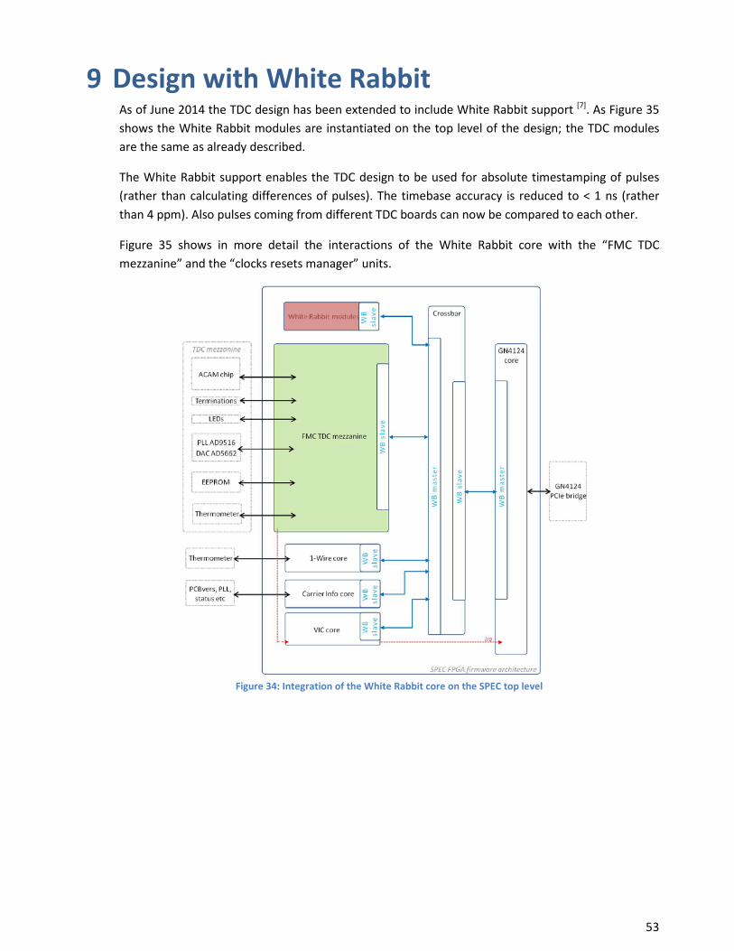
9 Design with White Rabbit As of June 2014 the TDC design has been extended to include White Rabbit support [7]. As Figure 35 shows the White Rabbit modules are instantiated on the top level of the design; the TDC modules are the same as already described.
The White Rabbit support enables the TDC design to be used for absolute timestamping of pulses (rather than calculating differences of pulses). The timebase accuracy is reduced to < 1 ns (rather than 4 ppm). Also pulses coming from different TDC boards can now be compared to each other.
Figure 35 shows in more detail the interactions of the White Rabbit core with the “FMC TDC mezzanine” and the “clocks resets manager” units.
Figure 34: Integration of the White Rabbit core on the SPEC top level
53
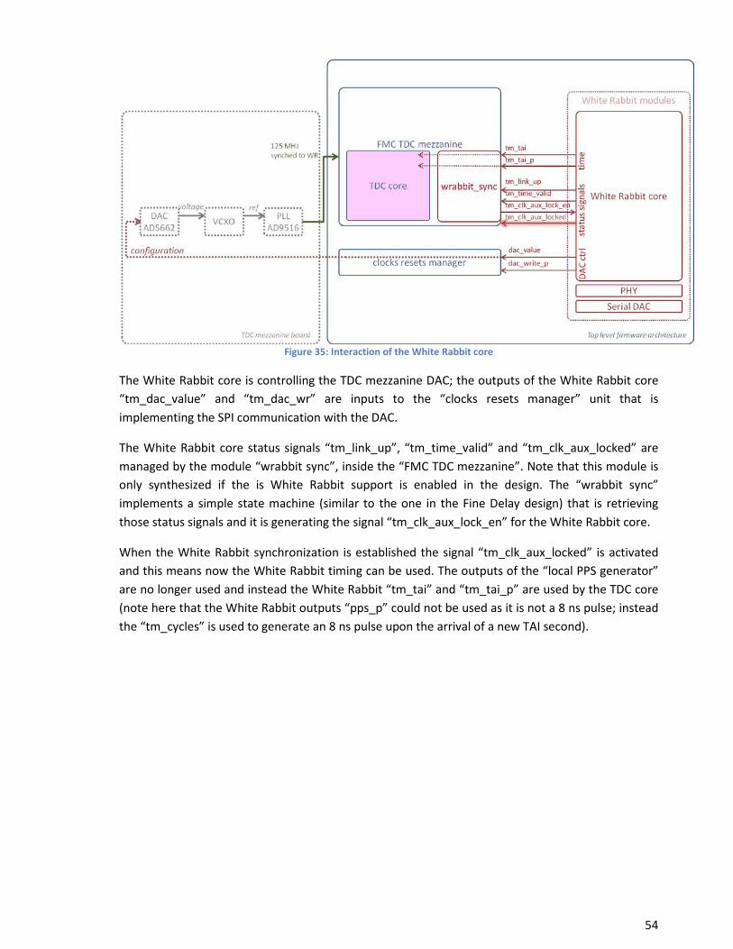
Figure 35: Interaction of the White Rabbit core
The White Rabbit core is controlling the TDC mezzanine DAC; the outputs of the White Rabbit core “tm_dac_value” and “tm_dac_wr” are inputs to the “clocks resets manager” unit that is implementing the SPI communication with the DAC.
The White Rabbit core status signals “tm_link_up”, “tm_time_valid” and “tm_clk_aux_locked” are managed by the module “wrabbit sync”, inside the “FMC TDC mezzanine”. Note that this module is only synthesized if the is White Rabbit support is enabled in the design. The “wrabbit sync” implements a simple state machine (similar to the one in the Fine Delay design) that is retrieving those status signals and it is generating the signal “tm_clk_aux_lock_en” for the White Rabbit core.
When the White Rabbit synchronization is established the signal “tm_clk_aux_locked” is activated and this means now the White Rabbit timing can be used. The outputs of the “local PPS generator” are no longer used and instead the White Rabbit “tm_tai” and “tm_tai_p” are used by the TDC core (note here that the White Rabbit outputs “pps_p” could not be used as it is not a 8 ns pulse; instead the “tm_cycles” is used to generate an 8 ns pulse upon the arrival of a new TAI second).
54

The calculations of a White Rabbit absolute timestamp are done the same way described in sections 3.1.2 and 3.1.10.
Figure 36: Timestamp calculations
An extensive study has shown that reading the Start01 upon the arrival of a timestamp is not essential, as it can be represented by a constant. The study was done by feeding a TDC input channel with the White Rabbit switch PPS output.
Figure 37: Connections between the White Rabbit switch and the SPEC-TDC
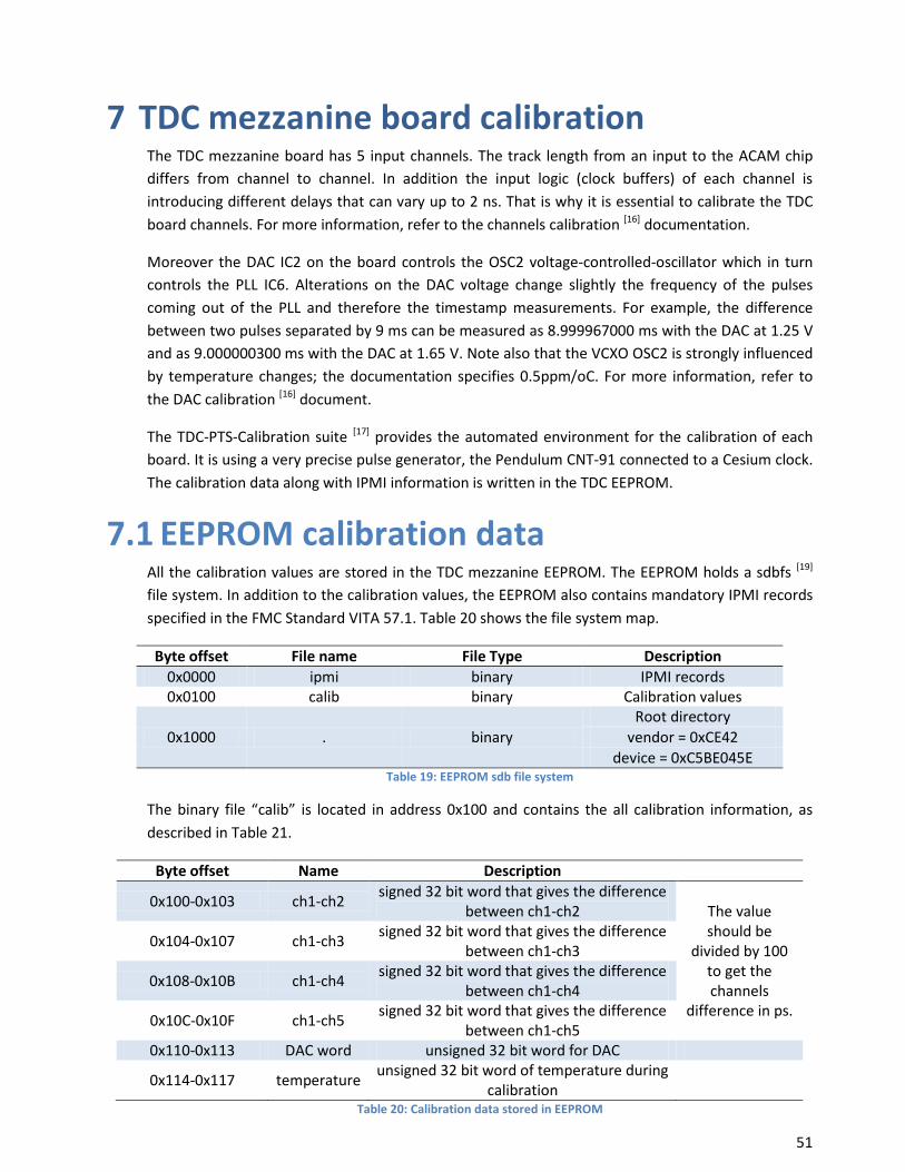
At the output of the switch, the White Rabbit PPS is synchronous to the White Rabbit TAI inside the TDC core. It arrives to the TDC input channel through a cable of a known length. Figure 38 shows the arrival of the pulses and Figure 39 shows an example of the expected timestamps.
Figure 38: Arrival of pulses
55
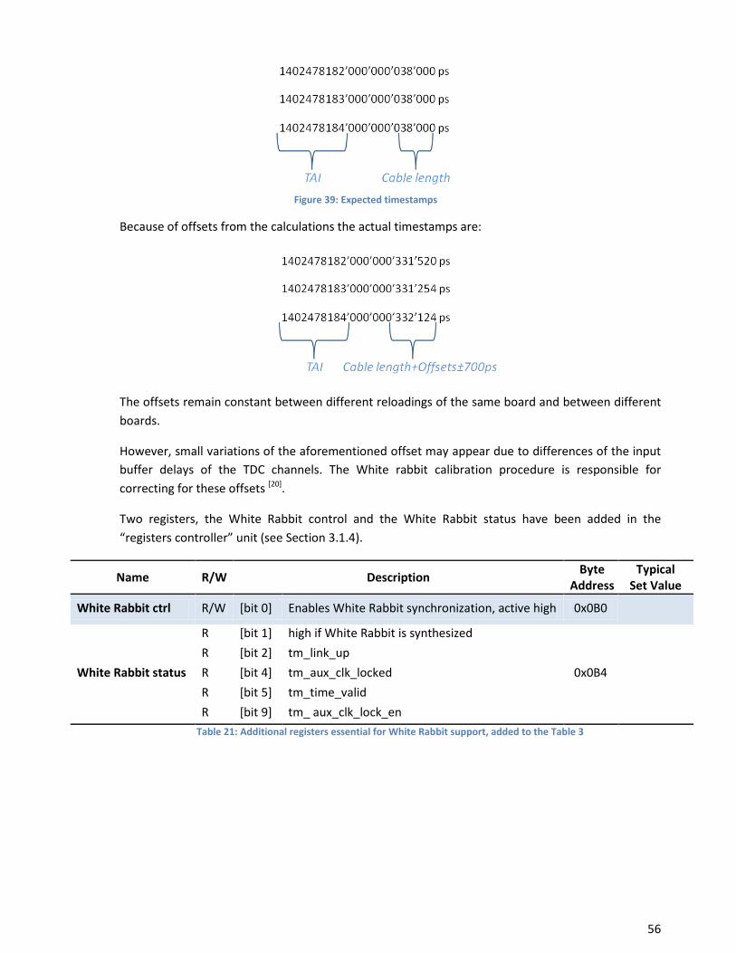
Figure 39: Expected timestamps
Because of offsets from the calculations the actual timestamps are:
The offsets remain constant between different reloadings of the same board and between different boards.
However, small variations of the aforementioned offset may appear due to differences of the input buffer delays of the TDC channels. The White rabbit calibration procedure is responsible for correcting for these offsets [20].
Two registers, the White Rabbit control and the White Rabbit status have been added in the “registers controller” unit (see Section 3.1.4).
Name R/W Description Byte
Address Typical
Set Value
White Rabbit ctrl R/W [bit 0] Enables White Rabbit synchronization, active high 0x0B0
White Rabbit status
R
R
R
R
R
[bit 1] high if White Rabbit is synthesized
0x0B4
[bit 2] tm_link_up
[bit 4] tm_aux_clk_locked
[bit 5] tm_time_valid
[bit 9] tm_ aux_clk_lock_en Table 21: Additional registers essential for White Rabbit support, added to the Table 3
56
10 References [1]: FMC projects: http://www.ohwr.org/projects/fmc-projects/wiki
[2]: SPEC board: http://www.ohwr.org/projects/spec/wiki
[3]: SVEC board: http://www.ohwr.org/projects/svec/wiki
[4]: ACAM TDC GPX: http://www.acam.de/fileadmin/Download/pdf/English/DB_GPX_e.pdf
[5]: FMC TDC software support: http://www.ohwr.org/projects/fmc-tdc-1ns-5cha-sw/wiki
[6]: GN4124 core: http://www.ohwr.org/projects/gn4124-core/wiki
[7]: The White Rabbit project: http://www.ohwr.org/projects/white-rabbit/wiki
[8]: Open cores One Wire master: http://opencores.org/project,sockit_owm
[9]: EEPROM 24AA64: http://ww1.microchip.com/downloads/en/devicedoc/21189f.pdf
[10]: Open cores I2C master: http://opencores.org/project,sockit_owm
[11]: SDB records: http://www.ohwr.org/projects/fpga-config-space/wiki
[12]: General cores library: http://www.ohwr.org/projects/general-cores
[13]: VME64x core: http://www.ohwr.org/projects/vme64x-core
[14]: TDC testing: http://www.ohwr.org/projects/fmc-tdc/wiki/Board_Performance
[15]: ACAM registers (pg. 17): http://www.acam.de/fileadmin/Download/pdf/English/DB_GPX_e.pdf
[16]: Calibration: http://www.ohwr.org/projects/fmc-tdc-1ns-5cha-
tst/repository/revisions/master/show/test/fmctdc1ns5cha/calibration/doc/CalibrationStudy
[17]: Calibration suite: http://www.ohwr.org/projects/fmc-tdc-1ns-5cha-
tst/repository/revisions/master/show/test/fmctdc1ns5cha/calibration
[18]: WISHBONE generator: http://www.ohwr.org/projects/wishbone-gen/wiki
[19]: SDBFS: http://www.ohwr.org/attachments/download/1594/sdbfs-2012-09-19.pdf
[20]: TDC White Rabbit calibration: http://www.ohwr.org/projects/fmc-tdc-1ns-5cha-
tst/repository/revisions/master/show/test/fmctdc1ns5cha/calibration/doc/CalibrationStudy
57

58