FM RDS macro component FM6A - gns-electronics · Diagram shows RDS sensitivity vs frequency....
18
FM RDS macro component FM6A confidential information final specification © GNS-Electronics GmbH 2018 V 1.7, Jun 14 2018 1 1. Introduction The GNS FM6A macro component is designed for easy integration of TMC functionality in your PDA/embedded or mobile navigation equipment. It provides extended features on chip-sized PCB space requirements. A software development kit (SDK) containing complete API functions for various O/S is also available from GNS for the TMC software integration. The GNS API is implemented in most portable dynamic navigation SW-products on the market, so units using FM6A will work without further SW development. 2. Compatibility with prev. FM6 hardware The new FM6A hardware replaces both FM6 and FM6V11 versions without any compatibility issues. 3. Features complete FM/RDS receiver module super miniature sized (9.3 * 10 *2.0 mm) type GNS protocol 3.0 1) enabled, allows GPS/RDS combined data over single UART. host computer (PDA / Notebook / embedded / phones) software API available for TMC application integration only one single power supply (2.9V..3.4V) low power consumption 75mW serial TTL/CMOS interface (3.3V) universal RAW RDS output high quality stereo audio output, DSP processor for IF,AF programmable audio volume A
Transcript of FM RDS macro component FM6A - gns-electronics · Diagram shows RDS sensitivity vs frequency....

FM RDS macro component FM6A confidential information final specification
© GNS-Electronics GmbH 2018
V 1.7, Jun 14 2018
1
1. Introduction
The GNS FM6A macro component is designed for easy integration of TMC
functionality in your PDA/embedded or mobile navigation equipment. It provides extended features on chip-sized PCB space requirements.
A software development kit (SDK) containing complete API functions for various O/S is also available from GNS for the TMC software integration.
The GNS API is implemented in most portable dynamic navigation SW-products on the market, so units using FM6A will work without further SW development.
2. Compatibility with prev. FM6 hardware
The new FM6A hardware replaces both FM6 and FM6V11 versions without any compatibility issues.
3. Features
complete FM/RDS receiver module
super miniature sized (9.3 * 10 *2.0 mm) type GNS protocol 3.0 1) enabled, allows GPS/RDS combined data over single UART.
host computer (PDA / Notebook / embedded / phones) software API available for TMC application integration
only one single power supply (2.9V..3.4V) low power consumption 75mW
serial TTL/CMOS interface (3.3V) universal RAW RDS output
high quality stereo audio output, DSP processor for IF,AF programmable audio volume
A

FM RDS macro component FM6A confidential information final specification
© GNS-Electronics GmbH 2018
V 1.7, Jun 14 2018
2
4. Applications
in-vehicle equipment for RDS TMC
dynamic navigation
handheld and notebook computers, mobile phones RDS TMC monitoring equipment (application software available)
5. Index 1. Introduction ..................................................................................................................... 1
2. Compatibility with prev. FM6 hardware ................................................................................ 1
3. Features .......................................................................................................................... 1
4. Applications ...................................................................................................................... 2
5. Index .............................................................................................................................. 2
6. Revision history ................................................................................................................ 3
7. Functional schematic ......................................................................................................... 3
8. Device pinout diagram ....................................................................................................... 4
9. Pin description .................................................................................................................. 4
10. Physical dimensions .......................................................................................................... 5
11. Recommended pad layout .................................................................................................. 6
12. Electrical specification ........................................................................................................ 7
13. ESD specification .............................................................................................................. 9
14. RDS performance diagram ................................................................................................. 9
15. Ordering information ......................................................................................................... 9
16. Application notes ............................................................................................................ 10
17. Startup timing ................................................................................................................ 11
18. Startup diagnostics ......................................................................................................... 11
19. Recommended PCB design ............................................................................................... 11
20. Material information ........................................................................................................ 12
21. Laser print device marking ............................................................................................... 12
22. Recommended soldering reflow profile ............................................................................... 13
23. Tape information ............................................................................................................. 14
24. Reel information ............................................................................................................. 15
25. Packing standard ............................................................................................................ 16
26. Firmware release information ........................................................................................... 17
27. Quality and Environmental Specifications ........................................................................... 17

FM RDS macro component FM6A confidential information final specification
© GNS-Electronics GmbH 2018
V 1.7, Jun 14 2018
3
6. Revision history
revision history V0.10 Aug 11 2006 P.Skaliks initial objective
V0.11 Oct 1 2006 P.Skaliks dimension correction
V1.00 Jan 3 2007 P.Skaliks final V1.00
V1.01 Jan 9 2007 P.Skaliks real Foto added,drawing corrected
V1.01 Jan 15 2007 obsolete Pin 11 removed from land pattern
V1.01 Jan 23 2007 P.Skaliks No of devices per reel raised to 2k
V1.02 Feb 12 2007 P.Skaliks firmware version 53
V1.03 Feb 20 2007 P.Skaliks esd information added
V1.05 Jun 11 2007 P.Skaliks FW V55
V1.06 Sep 25 2007 P.Skaliks Thickness of module corrected
V1.07 Sep 25 2007 P.Skaliks New part # assigned for V55
V1.08 Apr4,2008 P.Skaliks New additional part# for 9600bd GPS uart
V1.09 Apr 21 2008 P.Skaliks laser marking definition for 9600bd
V1.10 July,15,2008 P.Skaliks Vcc rise time definition
V1.15 Nov 12 2008 P.Skaliks MSL data added
V1.16 Nov 10 2010 P.Skaliks Packing data added , temp range edited,
V1.17 Dec 2 2010 P.Skaliks Schematic
V1.18 Dec 9 2010 P.Skaliks Solder profile
V1.19 Feb 24 12 P.Skaliks Dimensions formatting
V1.30 May 30 14 P.Skaliks Dimensions formatting
V1.40 Jan 12 15 P.Skaliks Added Index, diagnostic banner output
V1.50 Sep 18 17 M.Heinzel FM6A with emproved EMC, RFin allows no DC.
GNS–Electronics – new company appearance.
V1.60 Jan 17 2018 M.Heinzel FM6A complies to RED directive, no compatibility restrictions with previous
FM6 hardware.
V1.70 Jun 14 2018 M.Heinzel Overworked Quality and Environmental Specifications
7. Functional schematic
μController F301
Tuner chip
Si 4703
UART1 38400bps
UART2 4800 bps
4,5
3,6
RF in 1
AF out
8,9
GND RF GND
10
VCC
7 2
clock
FM6A
FM RDS macro component FM6A confidential information final specification
© GNS-Electronics GmbH 2018
V 1.7, Jun 14 2018
4
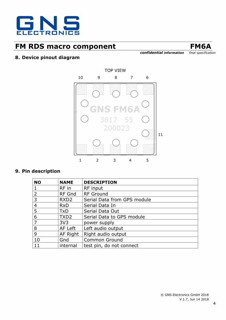
8. Device pinout diagram
TOP VIEW
9. Pin description
NO NAME DESCRIPTION
1 RF in RF input
2 RF Gnd RF Ground
3 RXD2 Serial Data from GPS module
4 RxD Serial Data In
5 TxD Serial Data Out
6 TXD2 Serial Data to GPS module
7 3V3 power supply
8 AF Left Left audio output
9 AF Right Right audio output
10 Gnd Common Ground
11 internal test pin, do not connect
1 2 3 4 5
10 9 8 7 6
11
GNS
0702 _00023
FM6 GNS 3817 55 200023
FM6A

FM RDS macro component FM6A confidential information final specification
© GNS-Electronics GmbH 2018
V 1.7, Jun 14 2018
5
10. Physical dimensions
1 2 3 4 5
10 9 8 7 6
11
GNS
3817 55 200023
FM6A
0.6 2.0
4.0
61.
6
10.0(+0.2)
1.8
3.6
5
9.0
(+
0.6
)
1.2
2.1
(+-0
.2) 0.8
3.0
0
1.20 x 1.30 *10

FM RDS macro component FM6A confidential information final specification
© GNS-Electronics GmbH 2018
V 1.7, Jun 14 2018
6
11. Recommended pad layout
0.6 2.0
4.0
61.
6
4.0
5.0
3.0
0.8
FM RDS macro component FM6A confidential information final specification
© GNS-Electronics GmbH 2018
V 1.7, Jun 14 2018
7
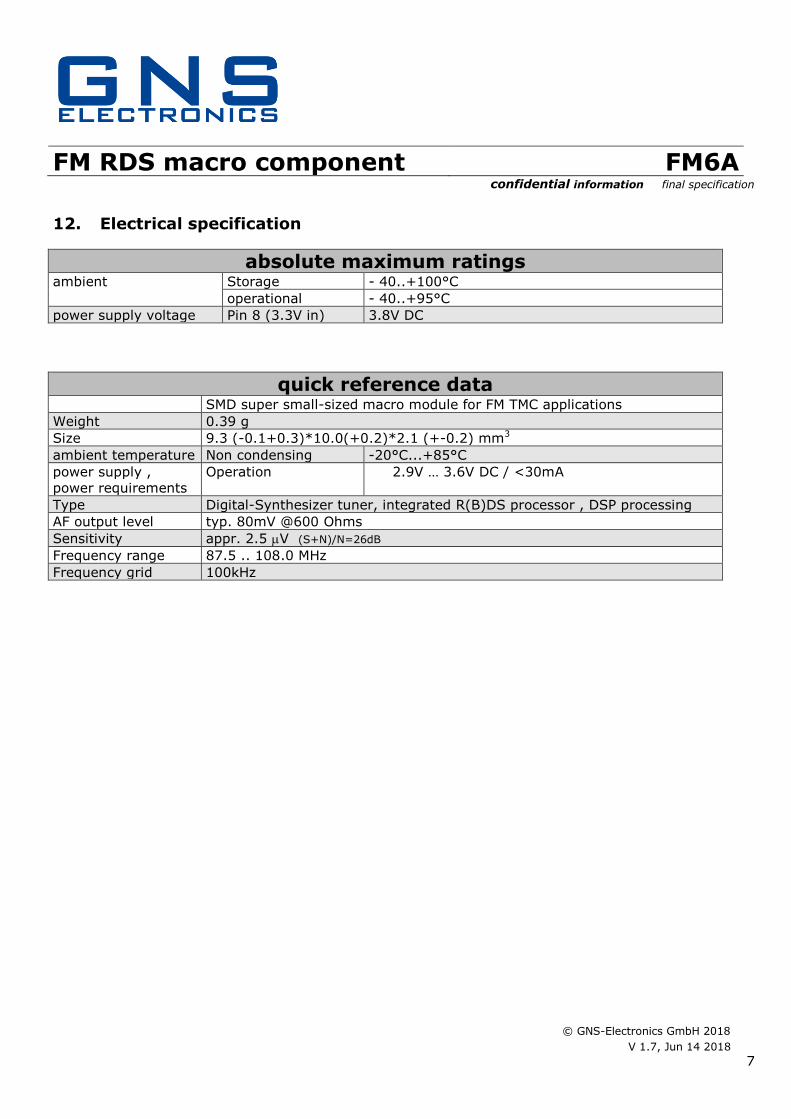
12. Electrical specification
absolute maximum ratings ambient Storage - 40..+100°C
operational - 40..+95°C
power supply voltage Pin 8 (3.3V in) 3.8V DC
quick reference data SMD super small-sized macro module for FM TMC applications
Weight 0.39 g
Size 9.3 (-0.1+0.3)*10.0(+0.2)*2.1 (+-0.2) mm3
ambient temperature Non condensing -20°C...+85°C
power supply ,
power requirements
Operation 2.9V … 3.6V DC / <30mA
Type Digital-Synthesizer tuner, integrated R(B)DS processor , DSP processing
AF output level typ. 80mV @600 Ohms
Sensitivity appr. 2.5 V (S+N)/N=26dB
Frequency range 87.5 .. 108.0 MHz
Frequency grid 100kHz

FM RDS macro component FM6A confidential information final specification
© GNS-Electronics GmbH 2018
V 1.7, Jun 14 2018
8
electrical data min typ max unit note
supply voltage Vcc 2.9 3.0 3.6 V
supply current 22 25 30 mA
Operating temperature -20 25 85 Typical, guaranteed
performance data
-40 - 95 Absolute maximum
-40 - 85 Tested for full performance, not
guaranteed, NO function
failures
Module setup delay time
after power up
- - 500 ms Host software should wait
before issueing first command
module Vcc supply rise
time
25 - 1000 µs 10..90% of Vcc
low level input voltage -0.5 - - V pin 3,4 serial CMOS Vcc=3.3V
high level input voltage 2.2 - Vcc+1.0V V pin 3,4 serial CMOS Vcc=3.3V
low level output voltage 0.0 - 0.7 V pin 5,6 serial CMOS Vcc=3.3V
high level output voltage Vcc-0.3 - Vcc-0.05 V pin 5,6 serial CMOS Vcc=3.3V
baud rate 38000 38400 38800 bit /sec other on demand
serial settings 8N1noP
Allowed DC input voltage
at RFin pin
- - 6 V Pin 1 Rfin
RF input resistance 3k 4k 5k Ohms VEMF=1mV,f= 87..108MHz,
guaranteed by
characterization
RF input capacitance 4 5 6 pF VEMF=1mV, guaranteed by
characterization
AF output voltage 70 80 90 mV RMS pins 8,9
AF output resistance - - 10 kOhms pins 8,9
AF THD - 0.1 0.5 %
AF (S+N) / N 57 63 - dB Vrf=1mV

FM RDS macro component FM6A confidential information final specification
© GNS-Electronics GmbH 2018
V 1.7, Jun 14 2018
9
13. ESD specification
esd data min unit pins reference
human body model 2000 V 3,4,5,6,7 JESD22-A114-B / C=100pF,
R=1k5
machine model 200 V 3,4,5,6,7 JESD22-A115-A / C=200pF, R=0r
human body model 2000 V 1,8,9 JESD22-A114 / C=100pF, R=1k5
machine model 250 V 1,8,9 JESD22-C101
14. RDS performance diagram
Diagram shows RDS sensitivity vs frequency. measurement under following
conditions: RF fed via coupled wire
RDS modulation is 2.7% of total modulation (75kHz) Criterion for RDS sensitivity is : 50% correct (no error) RDS groups
15. Ordering information
type part# laser
marking*
description
FM6A-001-G3 4037735106111 GNS FM6A
yyww ff
tttttt
data interface for serial TTL, GNS 3.0 Protocol,
GPS interface 4800bd
*ff = firmware ; yy = production year; mm = production month tttttt = tracecode, serial#
-100,0
-90,0
-80,0
-70,0
-60,0
-50,0
-40,0
87,5 92,5 97,5 102,5 107,5f[MHz]
level
dBm

FM RDS macro component FM6A confidential information final specification
© GNS-Electronics GmbH 2018
V 1.7, Jun 14 2018
10
16. Application notes
FM6A has been designed to enable portable navigation systems to operate
dynamically by the use of RDS-TMC traffic information. Two different typical application configurations can be used .
1. TWO- SERIAL- PORT CONFIGURATION
for example:
stand-alone portable Navigation equipment or PDA with integrated GPS receiver
2. SINGLE - SERIAL- PORT CONFIGURATION (WITH GNS 3.0 PROTOCOL
1) )
for example: external combined receiver with cable or BT-transceiver, stand alone Navigation with only one serial port.
38400bps GPS unit
cable (RS232 supported)
or BT transceiver
4800bps half duplex
GPS unit
COM1
host processor
COM2
38400bps
anybaud
MMI
(key,display)

FM RDS macro component FM6A confidential information final specification
© GNS-Electronics GmbH 2018
V 1.7, Jun 14 2018
11
17. Startup timing
Due to internal circuitry self test and firmware initialization, Module setup delay time
after power up as specified under electrical data has to be respected by driving software. Delay time has to be kept after power has stabilized before issueing
the first command. Especially in case of software controlled power supply for FM6A, you should take
care to implement a delay in software.
18. Startup diagnostics
After an successful power on reset, FM6A will output a start up information via the Tx pin of the UART. This banner is outputted without any command after internal
startup procedures are finished. FM6A will provide some information and also an error code if initialization could not be finished successfully.
19. Recommended PCB design
FM6A is easy to integrate and needs only single power supply. Please note the following design rules for proper operation
Do not connect RF GND (2) to common GND(10) RF GND should be connected to antenna connector ground pin only
care for clean supply line (7) ensure power-on rise time below 5ms
do not short-circuit AF-out PINs (8,9), leave open if not used connect common GND (10) to system ground with Ground plane of PCB
connect RFin PIN (1) to antenna connector with a short (below 15mm) or impedance- matched line.
Startup output Output meaning
GNS FM6 V55 – YY/WW – 0CD G0 Initialization successful GNS FM6 V55 - YY/WW - 0CC-4 G0
'Tuner not initialized' – Tuner device could not start successfully. The most likely explanation is failure of the internal xtal (for example xtal demage by excessive heat)
GNS FM6 V55 - YY/WW - 0CC-1 G0
'I2C error' – Internal I2C bus not working correctly, FM hardware problem or supply problem

FM RDS macro component FM6A confidential information final specification
© GNS-Electronics GmbH 2018
V 1.7, Jun 14 2018
12
20. Material information
complies to ROHS standard ROHS documentations are available on request
contact surface : gold over nickel
SHIELD MATERIAL INFORMATION "German Silver " , CuNi18Zn27
Cu: 53.5..56.5% Ni : 16.5..19.5%
Zn : 24..30% thickness :0.2mm
21. Laser print device marking
device name
date code
of
production
yyww /
optional
version
code
serial # of week
firmware
release #
55
A

FM RDS macro component FM6A confidential information final specification
© GNS-Electronics GmbH 2018
V 1.7, Jun 14 2018
13
22. Recommended soldering reflow profile
Notes:
1. FM6A should be soldered in upright soldering position. In case of head-over soldering, please prevent shielding / FM6A-Module from falling down.
2. Do never exceed maximum peak temperature 3. Reflow cycles allowed : 1
100
200
300
t[sec] 100 200
T[°C]
260°C max
250°C for 10 sec max
230°C for 40 sec max
160°C 190°C 120 sec
FM RDS macro component FM6A confidential information final specification
© GNS-Electronics GmbH 2018
V 1.7, Jun 14 2018
14
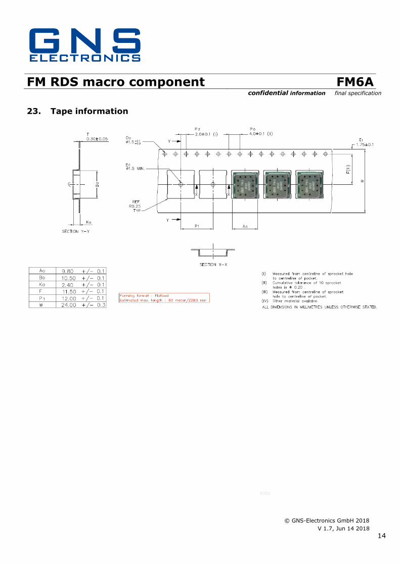
23. Tape information
0702 _00023

FM RDS macro component FM6A confidential information final specification
© GNS-Electronics GmbH 2018
V 1.7, Jun 14 2018
15
24. Reel information
no. of devices : 2000 pcs / reel

FM RDS macro component FM6A confidential information final specification
© GNS-Electronics GmbH 2018
V 1.7, Jun 14 2018
16
25. Packing standard
1 reel
contents 2,000pcs
GNS part# 2 x 6550000003
1x 6550000011
dimensions dia: 330mm thickness:30.4mm
gross weight 1.253 Kg with full contents
net weight 0.246 Kg
2 vacuum bag GNS part# 6550000006
dimensions 400mm x 480mm
gross weight 1.321 kg with full contents
net weight 0.068 Kg
air pressure level <30mbar
3 moisture indicator GNS part# 6550000008
dimensions 76mm x 51mm
weight 0.001 Kg
4 dry pack
GNS part# 6550000007
dimensions 145mm x 140mm
weight 0.068 Kg
5 Box for reel GNS part# 6550000012
dimensions 350 mm x 350mm x 47mm
gross weight 1.5357 kg with full contents
net weight 0.184 kg
6 Outer box contents max 7 box for reel (14,000 pcs FM6A)
dimensions 400mm x 370mm x 360mm
gross weight 11.6 kg with full contents
net weight 0.85 kg
special/smaller quantities packaging qty <=50 stripe(s) of tape will be directly vacuum
packed with vacuum bag, dry pack,
moisture indicator. staples of tape
allowed. minimum # parts per stripe is
10. vacuum bag size should fit for easy
transportation (A5..A4)
qty >50 tape will be full length (min 70%) on reel,
will be packed originally with 2,3,4,5
above

FM RDS macro component FM6A confidential information final specification
© GNS-Electronics GmbH 2018
V 1.7, Jun 14 2018
17
26. Firmware release information
This product is equipped with firmware V55 with optimized clock frequency
27. Quality and Environmental Specifications
Test Standard Parameters PCB Inspection IPC-6012B, Class 2. Qualification and Performance
Specification for Rigid Printed Boards - Jan 2007
Assembly
Inspection
IPC-A-610-D, Class 2 “Acceptability of
electronic assemblies”
Temperature
Range
ETSI EN 300 019-2-7 specification T 7.3 -30 °C, +25 °C, +85 °C, operating
Damp Heat ETSI EN 300 019-2-7 specification T 7.3 +70 °C, 80% RH, 96 hrs, non-operating
Thermal Shock ETSI EN 300 019-2-7 specification T 7.3 E -40 °C ... +85 °C, 200 cycles
Vibration ISO16750-3 Random vibration, 10~1000Hz, 27.8m/s2,
8hrs/axis, X, Y, Z 8hrs for each 3 axis non-
operating
Shock ISO16750-3 Half-sinusoidal 50g, 6ms, 10time/face,
±X, ±Y and ±Z non-operating
ESD Sensitivity JEDEC, JESD22-A114 ESD Sensitivity Testing Human
Body Model (HBM). Class 2
JEDEC, JESD22-A115 ESD Sensitivity Testing
Machine Model (MM), Class B
+2000V - Human hand assembly
+200V - Machine automatic final assembly
Moisture/Reflow
Sensitivity
IPC/JEDEC J-STD-020D.1 MSL3
Storage (Dry
Pack)
IPC/JEDEC J-STD-033C MSL3
Solderability EN/IEC 60068-2-58 Test Td More than 90% of the electrode should be cove-
red by solder. Solder temperature 245 °C ± 5 °C
Moisture Sensitivity
GNS ships all devices dry packed in tape on reel with desiccant and moisture level indicator sealed
in an airtight package. If on receiving the goods the moisture indicator is pink in color or a
puncture of the airtight seal packaging is observed, then follow J-STD-033 “Handling and Use of
Moisture/Reflow Sensitive Surface Mount Devices”.
Storage (Out of Bag)
The FM6A modules meet MSL Level 3 of the JEDEC specification J-STD-020D - 168 hours Floor Life
(out of bag) ≤30 °C/60% RH. If the stated floor life expires prior to reflow process then follow J-
STD-033 “Handling and Use of Moisture/Reflow Sensitive Surface Mount Devices”.

FM RDS macro component FM6A confidential information final specification
© GNS-Electronics GmbH 2018
V 1.7, Jun 14 2018
18
GNS-ELECTRONICS GMBH 2018
THE INFORMATION IN THIS DOCUMENTATION DOES NOT FORM ANY QUOTATION OR CONTRACT. TECHNICAL DATA ARE DUE TO BE CHANGED WITHOUT
NOTICE. NO LIABILITY WILL BE ACCEPTED BY THE PUBLISHER FOR ANY CONSEQUENCE OF THIS DOCUMENT'S USE. REPRODUCTION IN WHOLE OR IN PART IS PROHIBITED WITHOUT THE PRIOR WRITTEN CONSENT OF THE COPYRIGHT OWNER
1) note:
patented technology by GNS-Electronics GmbH