Flexible & Printed Electronics - SEMI.ORGregions.semi.org/eu/sites/semi.org/files/docs/Presentation...
38
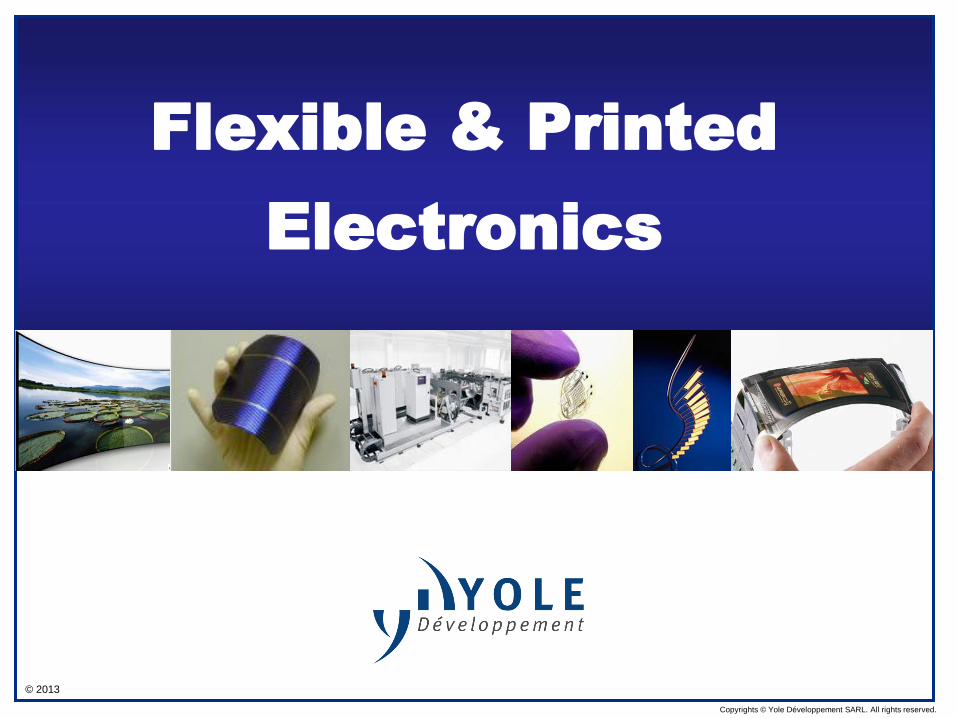
© 2013 Copyrights © Yole Développement SARL. All rights reserved. Flexible & Printed Electronics
Transcript of Flexible & Printed Electronics - SEMI.ORGregions.semi.org/eu/sites/semi.org/files/docs/Presentation...
© 2013
Copyrights © Yole Développement SARL. All rights reserved.
Flexible & Printed
Electronics

© 2013• 2
Fields of Research Activity
Founded in 1998, Yole Developpement is a global market, technology and strategy consulting company involved in :
Our research is performed by in-house personnel conducting open-ended discussions based on interviews.
32 full time analysts with technical and marketing degrees
Primary research including over 3,500 interviews per year
Wafers and Substrates
MEMS &
Image Sensors
Photovoltaics
Advanced
Packaging
Microfluidic
& Medical Technologies Power Electronics
HB LED, LED & LD

© 2013• 3
Our Global Activity
Yole Inc.
Yole Paris
Yole Japan
30% of our business is
in North America
30% of our business is
in Asia
40% of our business is
in EU Countries
Yole Korea Yole Développement Lyon HQ
Yole Taiwan
S+C

© 2013• 4
Mission Statement
Knowledged Based Company
• Help our customers develop their business through specific
analysis and reports by providing:
Accurate market data, market segmentation and marketing
analysis
Technical evaluation and technology cost and COO analysis
Patent portfolio analysis and freedom to operate analysis
Strategic analysis to enhance company and business unit
performances
Support strategic development: find growth opportunities, support
M&A and find new investors
Advertising opportunities in YOLE magazines, via webinar and
specific events
• Help them get operational results from our actions

© 2013• 5
Yole Activities
www.yole.fr
Technology & Market Reports
Report/Database/Reverse Costing/Tools
Custom Studies Market Research
Technology & Strategy
Yole Finance M&A / Due Diligence / Fund raising services
www.yolefinance.com
Media business Website / Magazines / Webcasts

© 2013• 6
ANNUAL ACTIONS
Research Products Content comparison
Custom analysis scope is
defined with you to meet your
information and budget needs
Breadth of the Analysis D
ep
th o
f th
e A
na
lys
is
CUSTOM
ANALYSIS
WORKSHOPS
STANDARD REPORTS Q&A
Services
© 2013• 7
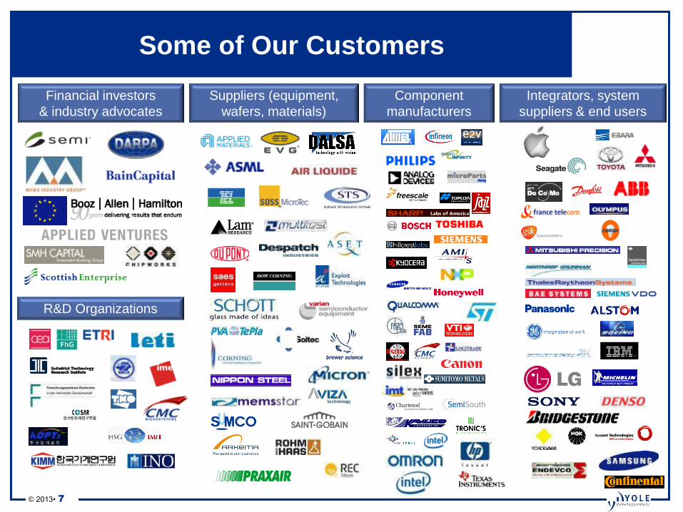
Some of Our Customers
Financial investors
& industry advocates
R&D Organizations
Suppliers (equipment,
wafers, materials)
Component
manufacturers
Integrators, system
suppliers & end users

© 2013• 8
Definitions
• In the report, we use the following definitions:
– Flexible electronics: Partly or completely flexible electronic devices.
Manufacturing process can include evaporation, MOCVD, solution printing etc.
– Printed electronics: Electronic devices using solution-based manufacturing
processes (screen printing, roll-to-roll, inkjet etc.). Although we do not consider
as printed devices products with only one printing step such as screen-printed
PV devices. Only the devices which have an active part made by printing
techniques are considered as “printed”. Therefore, for instance crystalline
silicon cells with screen printed metallization are not considered here.
– Polytronics: Formerly “Polymer Electronics”. They are devices mixing printed
electronics, flexible electronics, and inorganic electronics (standard Si ICs, thin
film technologies and so on… ).

© 2013• 9
APPLICATION LANDSCAPE
© 2013• 10
Application landscape (1/3)
Flexible
Application enabling / Function
enabling
Printed
(Potentially) Large volumes / Low
cost
Large OLED
Displays
TV
Small OLED
Displays
Mobile phones /
tablets
Conformable
Organic PV
Energy
harvesting
Large / high
volume
Organic PV
PV farms /
grid
electricity
OLED
Lighting
General
lighting
Systems on foil
Smart systems,
polytronics
Conformable
OLED Lighting
Automotive /
luxury lighting
Gas sensors
Wireless
sensors
Electronic
paper
e-readers

© 2013• 11
Application landscape (2/3)
• Market drivers for flexible and printed electronics are different, even though
manufacturing processes and end applications share similarities
• Main market drivers for flexible electronics are:
– The possibility to add new functionalities:
• Conformability for OLED lighting (for the automotive industry),
• Conformability for OPV (energy harvesting)
• Robustness for small OLED displays (for smart phones & tablets)
– The possibility to create new applications:
• wearable electronics.
– Flexible electronics is NOT meant to be low-cost, and usually uses expensive processes
(MOCVD, evaporation)
• The main market driver for printed electronics is:
– Cost reduction thanks to high volume (Roll-to-roll) manufacturing or to the fewer use of
expensive manufacturing processes (MOCVD, evaporation):
• potentially lower cost OLED TVs can be built if solution based manufacturing is mastered, potentially
low cost OPV can appear if technical challenges are leveraged
© 2013• 12
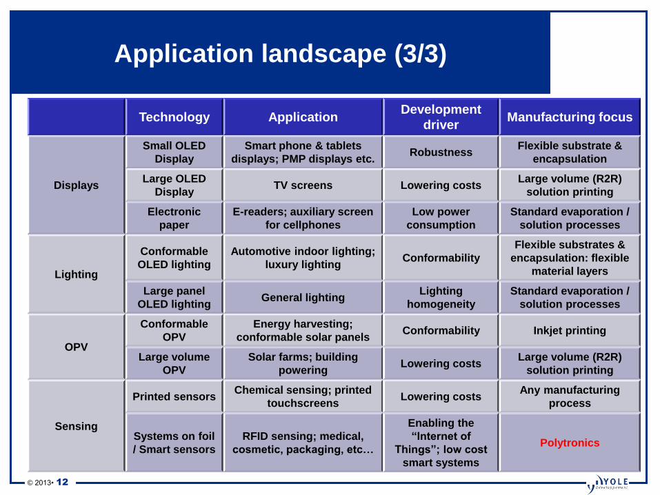
Application landscape (3/3)
Technology Application Development
driver Manufacturing focus
Displays
Small OLED
Display
Smart phone & tablets
displays; PMP displays etc. Robustness
Flexible substrate &
encapsulation
Large OLED
Display TV screens Lowering costs
Large volume (R2R)
solution printing
Electronic
paper
E-readers; auxiliary screen
for cellphones
Low power
consumption
Standard evaporation /
solution processes
Lighting
Conformable
OLED lighting
Automotive indoor lighting;
luxury lighting Conformability
Flexible substrates &
encapsulation: flexible
material layers
Large panel
OLED lighting General lighting
Lighting
homogeneity
Standard evaporation /
solution processes
OPV
Conformable
OPV
Energy harvesting;
conformable solar panels Conformability Inkjet printing
Large volume
OPV
Solar farms; building
powering Lowering costs
Large volume (R2R)
solution printing
Sensing
Printed sensors Chemical sensing; printed
touchscreens Lowering costs
Any manufacturing
process
Systems on foil
/ Smart sensors
RFID sensing; medical,
cosmetic, packaging, etc…
Enabling the
“Internet of
Things”; low cost
smart systems
Polytronics

© 2013• 13
PLAYERS LANDSCAPE

© 2013• 14
Players landscape (1/3)
Flexible
Application enabling / Function
enabling
Printed
(Potentially) Large volumes / Low
cost
Large OLED
Displays
Small OLED
Displays Conformable
Organic PV
Large / high
volume Organic
PV OLED Lighting
Systems on foil /
polytronics
Conformable
OLED Lighting
Gas sensors
Electronic
paper
© 2013• 15
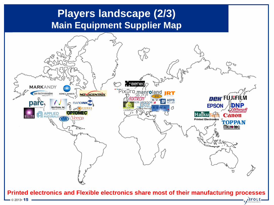
Players landscape (2/3) Main Equipment Supplier Map
Printed electronics and Flexible electronics share most of their manufacturing processes

© 2013• 16
Players landscape (3/3) Main Material Supplier Map
Printed electronics and Flexible electronics share the same manufacturing materials

© 2013• 17
Each Printed Electronics Segment Has Very
Complex Supply Chains
Example of ThinFilm Electronics NVRAM supply chain Unique to ThinFilm
If you want to play in
Printed Electronics, you
have to put your own
infrastructure together!
© 2013• 18
PRINTED ELECTRONICS APPLICATIONS

© 2013• 19
Printed electronics applications
© 2013• 20
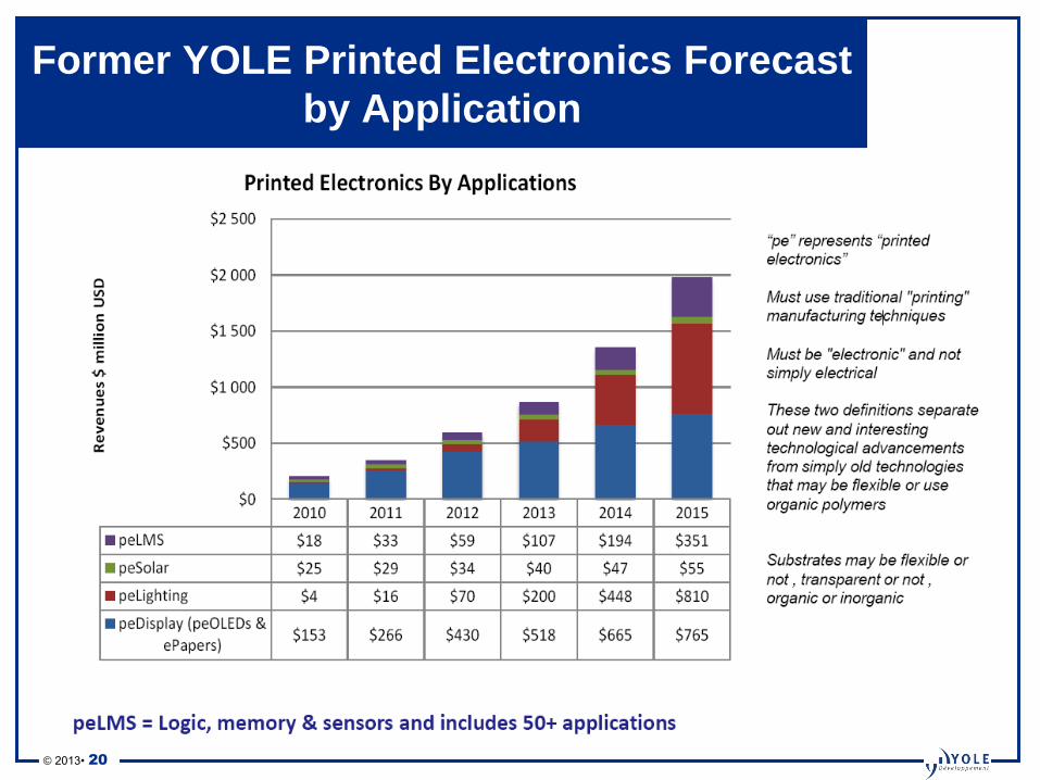
Former YOLE Printed Electronics Forecast
by Application

© 2013• 21
Technology needs always more time to
come to the market…

© 2013• 22
2013-2020 Flexible & Printed Electronics
Market
• Printed & Flexible Electronics is expected to be close to $1B market by 2020 with a
27% CAGR over 2013-2012
© Yole Développement 2013
2013 2014 2015 2016 2017 2018 2019 2020
TOTAL Flexible & Printed Electronics($M)
$ 176 $ 181 $ 189 $ 257 $ 338 $ 534 $ 749 $ 959
$ 00
$ 200
$ 400
$ 600
$ 800
$ 1 000
$ 1 200
US$
M
TOTAL Flexible & Printed Electronics (US$M)

© 2013• 23
PRINTED ELECTRONICS CHALLENGES:
TECHNICAL LIMITATIONS

© 2013• 24
Technical Limitations
• Materials performances
– High-performance materials are required for most
applications such as OLED displays for example.
– Solution materials have to keep from mixing with each other
– They have to stay contained in a pixels area for displays
– Etc…
• Appropriate equipment
– Appropriate printing equipment must be developed and
affordable.
– Printed electronics requires smaller pitches than what can
offer current printing pieces of equipment: graphic industry
does not need a precision under 40 μm
• High Volumes!
– For printed solutions to become affordable, high volumes
have to be reached, and this will not be the case at short /
mid term
In OLED Displays for example, high
intra-pixel uniformity is required,
which is not yet attainable with
current solutions.
Source: DuPont

© 2013• 25
Application Breakdown
© 2013• 26
FLEXIBLE ELECTRONICS CHALLENGES
© 2013• 27
Challenges for flexible electronics
• Flexible barriers
– The main challenge is on materials for encapsulation
– Current technologies are not so good when used on flexible devices
– Current options such as flexible glass or multi-layer technologies are expensive
– Active materials are required for higher performance applications such as OPV
or flexible OLED. No such material yet exists
• Some companies start to build production lines for flexible OPV in
2016+. Nevertheless these companies are betting on the hope that a
suitable barrier material will exist by the time the line is operational.

© 2013• 28
PRINTED ELECTRONICS CHALLENGE:
FINANCIAL INCOHERENCE

© 2013• 29
2013 Financial analysis • In last report, we tracked 24 companies for a total of US$1.35B raised over 2000-2010 (we did not
get the information for 3 companies).
• Two years later, 1 companies out of the 3 that had raised > $100M did bankrupt:
– Konarka (photovoltaics).
– Nanosolar starts layoffs in February 2013
– And PlasticLogic is currently trying to find new applications outside the e-readers market!
$422
$372
$180
$61 $59 $57$36 $34 $29 $25 $21 $10 $9 $8 $7 $6 $4 $3 $3 $3 $2
$0
$50
$100
$150
$200
$250
$300
$350
$400
$450
$500
Am
ou
t ra
ise
d (
US
$)
Total amount raised over 2000-2011(USD)Dow Jones Venture Source
? ?

© 2013• 30
EVOLUTION OF PRINTED ELECTRONICS:
POLYTRONICS

© 2013• 31
Polytronics definition
• Polytronics (Polymer Electronics) is the “evolution” of printed & flexible electronics.
We assimilate it to the also called “hybrid printed electronics”, it is the integration on
a flexible foil of different technologies:
– Printed devices (printed sensors, OPV)
– Si ICs
– Thin film technologies
– Etc…
• The main purpose of Polytronics is to develop smart systems with a potential low
cost, thus enabling larger visions such as “the Internet of Things” and even more.
• The global interest in polytronics is born from the difficulties faced by the flexible &
printed electronics industry. It is an alternate way to come to similar results while
trying to avoid some of the main challenges.

© 2013• 32
Time for disillusion:
- No killer applications
- Huge technical
challenges
- Low market pull
- Restructuration of the
market (companies
close)
Printed electronics
promises:
- Only a few potential
applications (OLED
displays, touchscreens)
Flexible electronics
promises:
- Not flexibility, but
robustness and
conformability.
Beginning of the Hype for
polytronics
Printed electronics, Flexible electronics &
Polytronics history
80’s 90’s 2000’s 2010’s 2020’s
Highly conductive
polymers start to be
investigated.
Printed electronics
promises:
- New applications
(Kodak’s first diode)
Beginning of the hype
Printed electronics
promises:
- New applications
- Low costs
Flexible electronics is
being investigated
In the hype!
Tremendous amounts
of money are being
invested. First
working prototypes
are demonstrated.
Start-ups are
popping-out
Printed electronics
promises:
- New applications
- Low costs
- Infinite potential
Beginning of the hype
for flexible electronics
Polytronics starts to
be investigated
First high volumes
in printed & flexible
electronics, in a few
applications only
Actual polytronics
challenges are
being revealed
Legend:
Printed electronics
Flexible electronics
Polytronics
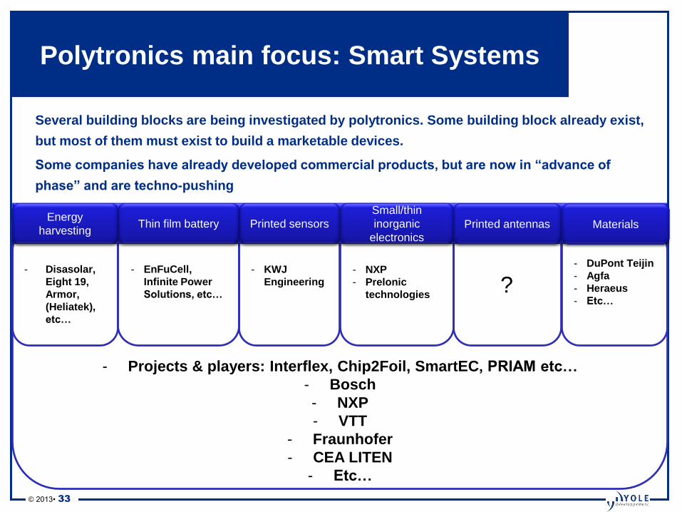
© 2013• 33
Several building blocks are being investigated by polytronics. Some building block already exist,
but most of them must exist to build a marketable devices.
Some companies have already developed commercial products, but are now in “advance of
phase” and are techno-pushing
- Projects & players: Interflex, Chip2Foil, SmartEC, PRIAM etc…
- Bosch
- NXP
- VTT
- Fraunhofer
- CEA LITEN
- Etc…
- EnFuCell,
Infinite Power
Solutions, etc…
- Disasolar,
Eight 19,
Armor,
(Heliatek),
etc…
- KWJ
Engineering
- NXP
- Prelonic
technologies
- DuPont Teijin
- Agfa
- Heraeus
- Etc…
Polytronics main focus: Smart Systems
Thin film battery Energy
harvesting
Small/thin
inorganic
electronics
Printed sensors Printed antennas Materials
?
© 2013• 34
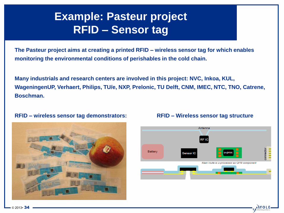
The Pasteur project aims at creating a printed RFID – wireless sensor tag for which enables
monitoring the environmental conditions of perishables in the cold chain.
Many industrials and research centers are involved in this project: NVC, Inkoa, KUL,
WageningenUP, Verhaert, Philips, TU/e, NXP, Prelonic, TU Delft, CNM, IMEC, NTC, TNO, Catrene,
Boschman.
RFID – wireless sensor tag demonstrators: RFID – Wireless sensor tag structure
Example: Pasteur project
RFID – Sensor tag

© 2013• 35
Polytronics current stage
• Pilot facilities are being developed, mixing roll-to-roll processes and pick & place for
inorganic components: VTT, Fraunhofer Institute, CEA LITEN, etc…
• Prototypes and start-ups start to appear:
– VTT and EnFuCell : biosensor coupled with electronics for cosmetic applications like
monitoring lotion penetration into the skin
– Fraunhofer EMFT: polytronics based Lab-on-a-chip
BUT
• Only niche applications have been identified. The only killer application could be
RFID if costs manage to go lower than Si-based RFID
• The technology is still at basic development stage
• Practical questions start to arise:
– Smart packages: How to recycle it? It cannot go into standard recycle bins…
– Smart clothing: Will it be trend-dependent and never last more than one season?
– Smart sensing: Is there an health issue if my kid tries to eat the sensor I put in my
refrigerator?

© 2013• 36
Surfing on the hype
1990 2000 2010 2020
Late 90’s: beginning of
the hype for printed
electronics
Start-ups start to be
created
2005-2008: In the hype for
printed electronics
Large investments in R&D
/ large investments in
start ups
2000’s: beginning of the
hype for flexible
electronics
Start-ups start to be
created
2012: End of the hype for
printed electronics
Industry restructuration /
companies start to close
2010’s: In the hype for
flexible electronics
Large investments in R&D
/ large investments in
start ups
2013: beginning of the
hype for polytronics
Start-ups start to be
created
Legend:
Printed electronics
Flexible electronics
Polytronics
Interest and investments

© 2013• 37
PE “At-a-glance”

© 2013• 38
DISCUSSION