Final Dissertation in Master
87
University of Mohamed Kheider of Biskra Exact Sciences and Sciences of Nature and Life Matter Sciences Final Dissertation in Master Matter Sciences Physics Energy Physics and Renewable Energies Presented by: NACEUR INTISSAR and ZERAOULIA MABROUKA Qualitative study of Indium Gallium Nitride (InGaN) – based solar cell. Jury: LAZNAK SAMIRA M.C. « A » Med Khider University- Biskra President MEFTAH AMJAD Professor Med Khider University- Biskra Supervisor BOUHDJAR ABDLFODHIL M.C. « B» Med Khider University- Biskra Examiner Academic Year:2018/2019
Transcript of Final Dissertation in Master

University of Mohamed Kheider of Biskra
Exact Sciences and Sciences of Nature and Life
Matter Sciences
Final Dissertation in Master
Matter Sciences
Physics
Energy Physics and Renewable Energies
Presented by:
NACEUR INTISSAR and ZERAOULIA MABROUKA
Qualitative study of Indium Gallium Nitride (InGaN) – based solar cell.
Jury:
LAZNAK SAMIRA M.C. « A » Med Khider University- Biskra President
MEFTAH AMJAD Professor Med Khider University- Biskra Supervisor
BOUHDJAR ABDLFODHIL M.C. « B» Med Khider University- Biskra Examiner
Academic Year:2018/2019


I
First, I thank Allah the completely powerful for having
agreed his infinite kindness, courage, the force and patience
to complete this modest work.
After that, I make a point of profoundly thanking to my
supervisor Miss Meftah Amjad for his help, support, guidance
and encouragement. She has been a great support on all
fronts and made my master dissertation journey a
memorable experience. I could not have imagined having a
better advisor and mentor for my Master study.
I am very grateful to the members of the jury: Doctor Laznak
Samira and Doctor Bouhdjar Abdlfodhil for accepting to
judge this thesis.
We also offer thanks to the PhD student who helped us and
wish her success in her scientific path and that Allah
preserves her.

II
To our support in life...
To those who taught us tender without waiting...
To whom we carry Their names with pride...
I hope of god to extend their age to see the fruits come harvest
after long waiting...
And your words will remain stars that I will guide today,
tomorrow and forever...
Our fathers
To the one who gave us love and affection…
To the source of The tenderness and the secret of existence...
To whom was Their prayer the secret of us success...
Our mothers.

IV
Figure I. 1: Transform solar energy into electric energy by the solar cell [11] ..................................... 2
Figure I. 2: Typical solar spectrum at the top of the atmosphere and at sea level. The difference is the
radiation absorbed/scattered by the atmosphere. The spectrum of a black body at 5250 C is also
superimposed and used for modeling. [13] ............................................................................................. 3
Figure I. 3:The air mass represents the proportion of atmosphere that the light must pass through
before striking the earth relative to its overhead path length, and is equal to 𝑌/𝑋. ................................ 4
Figure I. 4: A model showing the effect of air mass on the solar spectrum in the PV Lighthouse Solar
Spectrum Calculator[12]. ........................................................................................................................ 5
Figure I. 5:Structure of a photovoltaic cell. The respective dimensions of the different zones are not
respected [14]. ......................................................................................................................................... 5
Figure I. 6: The schematic structure of an idealized pin photodiode[15]. ............................................. 7
Figure I. 7: The short circuit current 𝐼𝑆𝐶 [12]. ...................................................................................... 8
Figure I. 8 :The open circuit voltage 𝑉𝑂𝐶 [12]. .................................................................................... 8
Figure I. 9: The fill factor FF[12]. ......................................................................................................... 9
figure I. 10: Spectral response schematic [12]. .................................................................................... 10
Figure II. 1: Band gap and the corresponding wavelength as a function of the lattice constant [21]. . 14
Figure II. 2: Plan views of zinc-blende (green) and wurtzite structures (pink) [24]. ........................... 15
Figure II. 3: Band gap energies determined for 𝐼𝑛𝑥𝐺𝑎1−𝑥 𝑁 films. Solid line is the fit using a bowing
parameter of 1.43 eV [36, 38, 39]. ........................................................................................................ 17
Figure II. 4: 𝐼𝑛𝐺𝑎𝑁 band gap as a function of 𝐼𝑛 concentration (𝑥𝐼𝑛). ................................................. 18
Figure II. 5: Absorption coefficient 𝛼 (cm-1) of 𝐼𝑛𝐺𝑎𝑁 versus wavelength (𝝀(µ𝒎)) for different
𝐼𝑛 compositions (𝑥𝐼𝑛) using the Matlab program and the equation (II.3). ............................................ 19
Figure II. 6: Extinction coefficient k of 𝐼𝑛𝐺𝑎𝑁 versus wavelength (𝝀(µ𝒎)) for different 𝐼𝑛
compositions (𝑥𝐼𝑛) using the Matlab program and the equation (II.8). ................................................. 20
Figure II. 7: Refractive index versus wavelength in the III-Nitrides group [25]. ................................ 21
Figure II. 8 : Refractive index of wurtzite 𝐼𝑛𝑥𝐺𝑎1−𝑥N, 𝐺𝑎𝑥𝐴𝑙1−𝑥 N 𝑎𝑛𝑑 𝐼𝑛𝑥𝐴𝑙1−𝑥 N alloys versus the
molar fraction(x) [25]. ........................................................................................................................... 21
Figure II. 9: Schematic structure of a) P-N 𝐼𝑛𝐺𝑎𝑁 Cell and b) P-I-N 𝐼𝑛𝐺𝑎𝑁 Cell. ........................... 24
Figure III. 1: Silvaco’s T CAD suite of tools [54]............................................................................... 29
Figure III. 2: The environment of the VWF[55].................................................................................. 30
Figure III. 3: Command group and statements layout for a Silvaco ATLAS file [57]. ....................... 31
Figure III. 4: Typical mesh in ATLAS. ............................................................................................... 32
Figure III. 5: Specified Regions. ......................................................................................................... 33
Figure IV. 1: 𝐼𝑛𝐺𝑎𝑁 based solar cell with homojunction PIN structure. ............................................ 40
Figure IV. 2: GaN/InGaN heterojunction solar cell with PIN structure. ............................................. 41
Figure IV. 3: GaN/InGaN double heterojunction solar cell with PIN structure. ................................. 42
Figure IV. 4: Structure of InGaN-based homojunction solar cell (structure A) under the Silvaco-Atlas
simulator. ............................................................................................................................................... 43

IV
Figure IV. 5: Spatial mesh of the homojunction solar cell (structure A) under the Silvaco-Atlas
simulator. ............................................................................................................................................... 43
Figure IV. 6: Structure of GaN/InGaN heterojunction solar cell (structure B) under the Silvaco-Atlas
simulator. ............................................................................................................................................... 44
Figure IV. 7: Spatial mesh of the heterojunction solar cell (structure B) under the Silvaco-Atlas
simulator. ............................................................................................................................................... 44
Figure IV. 8: Structure of the GaN/InGaN double heterojunction solar cell (structure C) under the
Silvaco-Atlas simulator. ........................................................................................................................ 45
Figure IV. 9: Spatial mesh of the double heterojunction solar cell (structure C) under the Silvaco-
Atlas simulator. ..................................................................................................................................... 45
Figure IV. 10: Extinction coefficient k in terms of wavelength 𝜆 for different concentrations of
indium 𝑥𝐼𝑛 according to theoretical calculations[40, 41]. .................................................................... 48
Figure IV. 11: Energy gap profile of the three studied cells at thermal equilibrium: (a)
structure A, (b) structure B and (c) structure C. .................................................................................... 49
Figure IV. 12: Current density - voltage (𝐽 − 𝑉) electrical characteristics of the studied solar cells A,
B and C with 𝑥𝐼𝑛=0.24 , 𝑥𝐼𝑛 = 0.34 𝑎𝑛𝑑 𝑥𝐼𝑛 = 0.57, under AM1.5 illumination. .............................. 50
Figure IV. 13: Power - voltage (𝑃 − 𝑉) characteristics of the studied solar cells A, B and C with
𝑥𝐼𝑛=0.24 , 𝑥𝐼𝑛 = 0.34 𝑎𝑛𝑑 𝑥𝐼𝑛 = 0.57, under AM1.5 illumination. .................................................... 51
Figure IV. 14: Solar cell output parameters vs Indium concetraction (𝑥𝐼𝑛) for structures A, B, and C :
a) Short circuit current, b) Open circuit voltage, c) Fill factor and d) Conversion efficiency . ........... 53
Figure IV. 15: Lifetime (and the corresponding𝑁𝑅) effects on the 𝐽𝑆𝐶 of the cell C optimized
with 𝑥𝐼𝑛 = 0.34. .................................................................................................................................... 56
Figure IV. 16: Lifetime (and the corresponding𝑁𝑅) effects on the 𝑉𝑜𝑐 of the cell C optimized
with 𝑥𝐼𝑛 = 0.34. .................................................................................................................................... 56
Figure IV. 17: Lifetime (and the corresponding𝑁𝑅) effects on the 𝐹𝐹 of the cell C optimized
with 𝑥𝐼𝑛 = 0.34. .................................................................................................................................... 57
Figure IV. 18: Lifetime (and the corresponding 𝑁𝑅) effects on the conversion efficiency of the cell C
optimized with 𝑥𝐼𝑛 = 0.34. ................................................................................................................... 58
Figure IV. 19: Solar cell output parameters vs 𝑃 − 𝐺𝑎𝑁 thickness for cell C: a)𝐽𝑠𝑐, b)𝑉𝑜𝑐, c) FF and
d) Efficiency. ......................................................................................................................................... 60
Figure IV. 20: Solar cell output parameters vs 𝐼 − 𝐼𝑛𝐺𝑎𝑁 thickness for cell C: a)𝐽𝑠𝑐, b)𝑉𝑜𝑐, c) FF
and d) Efficiency. .................................................................................................................................. 62

IV
Table I. 1: [1839-1904] Years of Discovery [4]..................................................................................... 2
Table I. 2: [1950-1954] Events of the years [4]. .................................................................................... 2
Table I. 3: The table presents some examples of solar cells and their efficiency. ............................... 11
Table II. 1: Junction band gaps and composition for ideal 𝐼𝑛𝑥𝐺𝑎1−𝑥 𝑁 multi-junction solar cells [5].
............................................................................................................................................................... 15
Table IV. 1: Simulation parameters associated with the cells studied taking into account the database
of Silvaco data. ...................................................................................................................................... 46
Table IV. 2: Cell output parameters variation for the structures A, B and C with changing the indium
molar fraction𝑥𝐼𝑛 .................................................................................................................................. 52
Table IV. 3: Lifetime effect on the output parameters (𝐽𝑆𝐶, 𝑉𝑂𝐶, 𝐹𝐹, 𝑃𝑚𝑎𝑥, 𝑎𝑛𝑑 𝜂 ) of the cell C
optimized with 𝑥𝐼𝑛 = 0.34. ................................................................................................................... 55
Table IV. 4: 𝑃 − 𝐺𝑎𝑁 layer thickness effect on the output parameters of the cell C optimized
with 𝑥𝐼𝑛 = 0.34. .................................................................................................................................... 59
Table IV. 5: 𝐼 − 𝐼𝑛𝐺𝑎𝑁 layer thickness effect on the output parameters of the cell C optimized
with 𝑥𝐼𝑛 = 0.34. .................................................................................................................................... 61

Acknowledgements ................................................................................................................... I
Dedication ................................................................................................................................. II
LIST OF FIGURES ............................................................................................................... III
LIST OF TABLES ................................................................................................................. IV
General introduction ............................................................................................................... X
Chapter I: Solar cells- an overview.
I.1 Introduction ..................................................................................................................... 1
I.2 History of solar cell ......................................................................................................... 1
I.3 What do we mean by the solar cell? .............................................................................. 2
I.4 Solar spectrum ................................................................................................................ 3
I.5 The air mass ..................................................................................................................... 4
I.6 Solar cell work ................................................................................................................. 5
I.7 Pin diode solar cells ......................................................................................................... 6
I.8 Solar cell parameters ...................................................................................................... 7
I.8.1 Short circuit current 𝑰𝑺𝑪 ......................................................................................... 7
I.8.2 Open circuit voltage 𝑽𝑶𝑪 ......................................................................................... 8
I.8.3 The fill factor 𝑭𝑭 ....................................................................................................... 9
I.8.4 Energy conversion efficiency 𝜼 ................................................................................ 9
I.8.5 The spectral response 𝑹𝑺 ....................................................................................... 10
I.9 Examples of solar cells .................................................................................................. 11
I.10 Conclusion .................................................................................................................... 12
Chapter II: Indium Gallium Nitride(InGaN) for Solar cells.
II.1 Introduction .................................................................................................................. 14
II.2 The Indium Gallium Nitride (𝑰𝒏𝒙𝑮𝒂𝟏−𝒙𝑵)Alloy ...................................................... 14
II.2.1 InxGa1-xN: An Overview ...................................................................................... 14
II.2.2 The band gap of𝑰𝒏𝒙𝑮𝒂𝟏−𝒙𝑵 ................................................................................. 16
II.2.3 Absorption coefficient and refractive index of 𝑰𝒏𝒙𝑮𝒂𝟏−𝒙𝑵 .............................. 18
𝑰𝑰. 𝟐. 𝟒 𝑰𝒏𝟏−𝒙𝑮𝒂𝟏−𝒙𝑵 Film growth ................................................................................. 22
II.2.5 Buffer layers .......................................................................................................... 22
II.2.6 Substrate growth ................................................................................................... 23
II.3 Performance of Current of 𝑰𝒏𝒙𝑮𝒂𝟏−𝒙𝑵 Solar Cells ................................................. 23

II.3.1 Comparison between PN and PIN ....................................................................... 24
II.4 Conclusion .................................................................................................................... 25
Chapter III: Digital Simulation software: Silvaco-Atlas.
III.1 Introduction ................................................................................................................ 27
III.2 Modeling today ........................................................................................................... 27
III .3 SILVACO ................................................................................................................... 28
III.3.1 The simulation tools (VWF CORE TOOLS) .................................................... 29
III.3.2 Interactive tools (VWF INTERACTIVE TOOLS)........................................... 30
III.3.3 Automation tools (VWF AUTOMATION TOOLS) ........................................ 30
III.4 Working with Atlas .................................................................................................... 31
III.4.1 Mesh ...................................................................................................................... 32
III.4.2 Region ................................................................................................................... 33
III.4.3 Contacts ................................................................................................................ 34
III.4.4 Doping ................................................................................................................... 34
III.4.5 Material ................................................................................................................ 34
III.4.6 Models ................................................................................................................... 35
III.4.7 Light Beam ........................................................................................................... 35
III.4.8 Solution Method ................................................................................................... 36
III.4.9 Solution Specification .......................................................................................... 36
The LOG .............................................................................................................................. 36
The SOLVE .......................................................................................................................... 36
The LOAD and SAVE ......................................................................................................... 37
III.4.10 Data Extraction and Plotting ............................................................................ 37
Extract .................................................................................................................................. 37
TonyPlot ............................................................................................................................... 37
Chapter IV: Qualitative study of Indium Gallium Nitride (InGaN) – based solar cell.
IV.1 Introduction ................................................................................................................ 39
IV.2 Simulation Parameters ............................................................................................... 39
IV.2.1 Structures Specifications ..................................................................................... 39
Structure A ........................................................................................................................... 39
Structure B ........................................................................................................................... 40
Structure C ........................................................................................................................... 41
IV.2.2 Input Parameter values ....................................................................................... 46
IV.3 Results and discussions .............................................................................................. 48
IV.3.1 Effect of defects .................................................................................................... 54

IV.3.2 Effect of 𝑷 – 𝑮𝒂𝑵 layer thickness ...................................................................... 58
IV.3.3 Effect of 𝑰 – 𝑰𝒏𝑮𝒂𝑵 layer thickness ................................................................... 60
IV.4 Conclusion ................................................................................................................... 63
General conclusion ................................................................................................................. 65
REFERENCES ....................................................................................................................... 66
Abstract ................................................................................................................................... 67
Résumé ..................................................................................................................................... 67

General introduction

X
The importance of energy in our society has become evident in the last few years. Among
the different alternative energies, solar energy has the very desirable property of being
essentially unlimited and of being neither polluting nor physically dangerous [1]. It is the source
of life. An amazing resource radiates energy and provides us with heat and light by
incorporating hydrogen into helium in essence. We call this solar radiation. Only about half of
this solar radiation makes it reach the Earth's surface. The rest is absorbed or reflected in clouds
and the atmosphere. However, we receive sufficient energy from the sun to meet the energy
requirements of all mankind - millions of times. Solar energy - energy from the sun - is a vast,
inexhaustible and clean resource.
Sunlight, or solar energy, can be used directly for heating and lighting homes and
businesses, for generating electricity, and for hot water heating, solar cooling, and a variety of
other commercial and industrial uses. Most critical, given the growing concern over climate
change, is the fact that solar electricity generation represents a clean alternative to electricity
from fossil fuels, with no air and water pollution, no global warming pollution, no risks of
electricity price spikes, and no threats to our public health [2].
Today, solar cells are highlighted, which are electronic devices that convert solar energy into
electrical energy. There are several types of solar cells based on different semiconductor
materials for example: Indium Gallium Selenide (𝐶𝐼𝐺𝑆), Gallium Arsenide(𝐺𝑎𝐴𝑠), silicon
(𝑆𝑖 )...etc. In our work, we will investigate the indium gallium nitride (𝐼𝑛𝐺𝑎𝑁)-based solar
cells. The 𝐼𝑛𝐺𝑎𝑁 solar cells promise a theoretical conversion efficiency relatively higher than
traditional Si based solar cells [3]. The 𝐼𝑛𝐺𝑎𝑁 material system offers a substantial potential to
develop ultra-high efficiency solar cells. It has a wide band gap ranging from [0.7-3.4 eV]. Most
uses of these solar cells are in space applications.
However, efficiency of experimental 𝐼𝑛𝐺𝑎𝑁 solar cells is lower than expected. The
theoretical maximum solar cell efficiency limit for a single junction has been shown to be 33.5
% [4] but the experimental efficiency closer to reality is less .
Based on the above, our study will focus on the quantitative study of Indium Gallium
Nitride

(𝐼𝑛𝐺𝑎𝑁) based solar cells, by simulation using Silvaco-Atlas software. The manuscript is
consisting of a general introduction and conclusion, in addition to four chapters organized as
follows:
❖ The first chapter presents an overview on the solar cells including their principle,
electrical characteristics, operation mode and a comparison between some examples of the solar
cells.
❖ The second chapter is devoted to the Indium Gallium Nitride (𝐼𝑛𝐺𝑎𝑁) alloy properties
and concepts as a promising material for solar cells.
❖ The third chapter is a simple exhibition of the Silvaco- Atlas simulation software, and
its implementation as part of our work.
❖ The fourth chapter presents the main part of our work on the investigation of
𝐼𝑛𝐺𝑎𝑁 based solar cells, with discussion and comments on the major results obtained from our
study.

Chapter I:
Solar cells- an
overview.

Solar cells- an overview.
1
Chapter I
I.1 Introduction
Each year, Earth receives a huge amount of solar energy. In order to use, we must Change
it to another format that can be used by our devices, for example, electricity (photovoltaic solar
energy)[5]. Earth receives an incredible supply of solar energy
The sun that is an intermediate star is a fusion reactor burn more than 4 billion years. It provides
sufficient energy in One minute to provide the world's energy needs for one year. In fact, "the
amount of solar radiation hit the earth over a three-day period is equivalent to energy stored in
all fossil energy sources." [6]. solar energy becomes the earth’s major renewable energy
resource, and the exploitation of the energy from the sun is the potential key to a sustainable
energy production in future, where solar energy offers a very large amount of technical potential
of over1000 EJ which is near twice the 2010 global primary energy supply of 510 EJ[7]. In this
chapter, we give an overview of some concepts related to solar cells.
I.2 History of solar cell
The solar cell industry has been so small that the first ban on Arab oil has been imposed
in 1973. Until then, the solar cell industry established a foothold Low level but steady cell
production and range and performance [8]. How the history of solar cells began and how they
evolved?
In 1839 Alexander Edmund Beckerle noted Photovoltaic (PV) effect by an electrode in a light
conductive solution. It is useful to look at the history of photovoltaic cells since that time there
are lessons to be learned which could provide guidance for future development Photovoltaic
cells. Table I.1 Gives developments during the time domain from [1839 − 1904], and the table
I.2 summarizes the events between 1950 and 1954 [9]. Since we will talk about the solar
cells𝐼𝑛𝐺𝑎𝑁, we have to mention a small piece about them. It was first dealt with 𝐺𝑎𝑁 in 1969
by setting it up for optical and electrical characterization. This was done by Maruska and
Tietjen[8]. After a good discovery of its characteristic and band gap 𝐸𝑔 = 3.39𝑒𝑣 , Adding the
indium (𝐼𝑛𝑥) element to the 𝐺𝑎1−𝑥𝑁 led to the opening of the band gap (0.4 − 3.4) eV.

Solar cells- an overview.
2
Chapter I
Table I. 1: [1839-1904] Years of Discovery [4].
1839 Alexandre Edmond Becquerel observes the photovoltaic effect via an
electrode in a conductive solution exposed to light.
1877 W.G. Adams and R.E. They observed the photovoltaic effect in solidified
selenium and published a paper on the selenium cell. ‘The action of light on
selenium’, in‘‘Proceedings of the Royal Society’’.
1883 Charles Fritts develops a solar cell using selenium on a thin layer of gold to
form a device giving less than 1 % efficiency.
1904 Wilhelm Hallwachs makes a semiconductor-junction solar cell (copper and
copper oxide).
Table I. 2: [1950-1954] Events of the years [4].
I.3 What do we mean by the solar cell?
Photovoltaics is the field of technology and research related to the devices, which directly
convert sunlight into electricity. It is the elementary building block of the photovoltaic
technology. In addition, they are made from semiconductors materials. We can also provide a
simple definition of the solar cell; A PV solar cell is a device that converts energy directly
electromagnetic (solar radiation) in direct electrical energy directly usable (Figure I.1) [10, 11].
Figure I. 1: Transform solar energy into electric energy by the solar cell [11]
Solar EnergyConversion device (Solar
Cell PV)Electric energy
1950 Bell labs produce solar cells for space activities.
1953 1953—Gerald Pearson begins research into lithium-silicon photovoltaic
cells.
1954 Bell labs announce the invention of the first modern silicon solar cell. These
cells have about 6 % efficiency.

Solar cells- an overview.
3
Chapter I
I.4 Solar spectrum
The solar spectrum changes throughout the day and with the location. Standard reference
spectra are defined to allow the performance comparison of photovoltaic devices from different
manufacturers and research laboratories. The standard spectra were refined in the early 2000s
to increase the resolution and to coordinate the standards internationally. The previous solar
spectrum, ASTMG159, was withdrawn from use in 2005. In most cases, the difference between
the spectrum has little effect on device performance and the newer spectra are easier to use[12].
The spectrum outside the atmosphere, the 5,800 K black body, is referred to as "𝐴𝑀0", meaning,
"zero atmospheres". Cells used for space power applications, like those on communications
satellites are generally characterized using𝐴𝑀0.
The spectrum after traveling through the atmosphere to sea level with the sun directly overhead
is referred to as "𝐴𝑀1". This means "one atmosphere"[13]. A typical solar spectrum, as a plot
of spectral irradiance vs wavelength, is shown in figure I.2.
Figure I. 2: Typical solar spectrum at the top of the atmosphere and at sea level. The
difference is the radiation absorbed/scattered by the atmosphere. The spectrum of a black
body at 5250 C is also superimposed and used for modeling. [13]

Solar cells- an overview.
4
Chapter I
I.5 The air mass
The Air Mass is the path length which light takes through the atmosphere normalized to
the shortest possible path length (that is, when the sun is directly overhead). The Air Mass
quantifies the reduction in the power of light as it passes through the atmosphere and is absorbed
by air and dust. The Air Mass is defined by:
𝐴𝑀 =1
𝐶𝑂𝑆 (𝜃)= √
ℎ2+𝑠2
ℎ2= √1 +
𝑠2
ℎ2 (I.1)
Where 𝜃 is the angle from the vertical (zenith angle). When the sun is directly overhead, the
Air Mass is one [13].
Figure I. 3:The air mass represents the proportion of atmosphere that the light must pass
through before striking the earth relative to its overhead path length, and is equal to 𝑌/𝑋.
The standard spectrum at the ground level is called 𝐴𝑀1.5𝐺 (G means the total consisting of
the direct and scattered vehicle) or 𝐴𝑀1.5𝐷 (which contains the direct vehicle only). Generally
approximates to 1 kW/𝑚2.

Solar cells- an overview.
5
Chapter I
Figure I. 4: A model showing the effect of air mass on the solar spectrum in the PV
Lighthouse Solar Spectrum Calculator[12].
The solar spectrum outside the solar envelope is called AM0 because there is no atmosphere
that is traversed by solar radiation. This spectrum is used to predict the performance of solar
cells in space.
I.6 Solar cell work
The solar cell is an electronic compound that converts sunlight directly into electricity. The
bright light on the cell produces both current and voltage to generate electrical power. This first
requires a light-absorbing material that can transfer the electron to a higher energy level and
secondly move this electron from the cell to an external circuit. This electron then expels its
energy in the outer circuit and returns to the cell. Semi-conveyors in the form of a p-n junction
carried out virtually all solar transformations.
Figure I. 5:Structure of a photovoltaic cell. The respective dimensions of the different zones
are not respected [14].

Solar cells- an overview.
6
Chapter I
Incident photons create carriers in areas N and P and in the zone of space charge. Photo-carriers
will behave differently depending on the region:
❖ In zone N or P, the minority carriers who reach the zone of space charge are "sent" by
the electric field in the p area (for holes) or in zone n (for electrons) where they will be the
majority. We will have a diffusion photocurrent.
❖ In the space charge area, the electron/hole pairs created by the incident photons are
dissociated by the electric field: his electrons will go to region n, the holes to the region p. we
will have a photocurrent generation.
These tow contributions are added to give a resulting photocurrent𝐼𝑝ℎ. It is a current of minority
carriers. It is proportional to the light intensity [14].
I.7 Pin diode solar cells
The pin diode is a device that has a structure with three distinct layers: a heavily doped thin
𝑝+-type layer, a relatively thick intrinsic (i) layer, and a heavily doped thin 𝑛+-type layer, as
shown in the figure I.6. When the structure is first formed, holes diffuse from the 𝑝+-side and
electrons from the 𝑛+-side into the i layer where they recombine and disappear. This leaves
behind a thin layer of exposed negatively charged acceptor ions in the 𝑝+-side and a thin layer
of exposed positively charged donor ions in the 𝑛+-side. The two charges are separated by the
I layer of thickness W. There is a uniform built in the field 𝐸0 in the i layer from the exposed
positive ions to the exposed negative ions, since there is no net space charge in the i layer, from:
𝑑𝐸
𝑑𝑥=
𝜌
𝜀0𝜀𝑟= 0 (I.2)
The field must be uniform, in contrast, the built –in field in the depletion layer of a pn junction
is not uniform [15].

Solar cells- an overview.
7
Chapter I
Figure I. 6: The schematic structure of an idealized pin photodiode[15].
I.8 Solar cell parameters
The main characteristic quantities of solar cells are:
Short circuit current 𝑰𝑺𝑪
Open circuit voltage 𝑽𝑶𝑪
The fill factor 𝑭𝑭
Energy conversion efficiency 𝜼
The spectral response 𝑹𝑺
I.8.1 Short circuit current 𝑰𝑺𝑪
The short-circuit current expressed in 𝑚𝐴 is the current flowing in the cell under
illumination and by shorting the terminals of the cell. It grows linearly with the illumination
intensity of the cell and it depends on the illuminated surface, the wavelength of the radiation,
the mobility of the charge carriers and the temperature. It can also be said that the current is the
current initiated by the cell under illumination in reduce output. Which means:
𝐼𝑆𝐶 = 𝐼(𝑉 = 0) and equations analytical:
𝐼 = 𝐼𝑝ℎ − 𝐼𝑆𝐶(𝑒𝑉 𝑉𝑇⁄ − 1) (I.3)

Solar cells- an overview.
8
Chapter I
Figure I. 7: The short circuit current 𝐼𝑆𝐶 [12].
I.8.2 Open circuit voltage 𝑽𝑶𝑪
The open circuit voltage 𝑉𝑂𝐶 is the maximum voltage available from a solar cell, and this
occurs at zero current. The open circuit voltage expresses the direct polarization of the resulting
cell by polarizing the junction with the light -generated current. The schematic of the open
circuit voltage on the I-V curve is in figure I.9.
𝐼0 (𝑒𝑒𝑉𝑜𝑐𝜂𝑘𝑏𝑇 − 1) − 𝐼𝑆𝐶 = 0 (I.4)
𝑉𝑂𝐶 =𝜂.𝐾𝑏.𝑇
𝑒𝑙𝑛 (
𝐼𝑆𝐶
𝐼0− 1) (I.5)
Figure I. 8 :The open circuit voltage 𝑉𝑂𝐶 [12].

Solar cells- an overview.
9
Chapter I
I.8.3 The fill factor 𝑭𝑭
The "fill factor" is the ratio of maximum power𝑃𝑚, to the open-circuit 𝑉𝑜𝑐voltage and short
circuits current𝐼𝑆𝐶 . It is known by the abbreviation "𝐹𝐹".² the 𝐹𝐹 is illustrated in figure I.9.
𝐹𝐹 =𝐼𝑚𝑉𝑚
𝑉𝑜𝑐𝐼𝑚=
𝑃𝑚
𝑉𝑜𝑐𝐼𝑠𝑐 (I.6)
In the ideal case, the fill factor (FF) is100 %. For a silicon solar cell, the 𝐹𝐹 typically ranges
between77.0% and 82.0%.
Figure I. 9: The fill factor FF[12].
I.8.4 Energy conversion efficiency 𝜼
Conversion efficiency is the most commonly used medium or benchmark for comparing a
solar cell to another. The efficiency represents the ratio between the electrical capacity
generated by the cell and the photovoltaic power it receives. Therefore, it depends on the
intensity of incoming light and the temperature of the solar cell. Therefore, the conditions under
which cell efficiency is measured to compare a cell to another must be controlled. In general,
solar cell efficiencies are measured at 25 ° C and AM1.5 light. In space, light is𝐴𝑀0.
𝜂 =𝐹𝐹.𝑉𝑂𝐶.𝐼𝑠𝑐
𝑃𝑖𝑛𝑐=
𝑃𝑜𝑢𝑡𝑚𝑎𝑥
𝑝𝑖𝑛𝑐 (I.7)

Solar cells- an overview.
10
Chapter I
I.8.5 The spectral response 𝑹𝑺
Quantitative efficiency gives the ratio between the number of electrons given by the cell
and the number of photons contained in it, whereas the spectral response is the ratio between
the electricity generated by the cell and the optical capacity of the incoming photons. In the
figure, we show an example of the silicon spectral response. The spectral response is limited to
long wavelengths because half of the carrier cannot absorb photons with lower-than-band
capacity. However, unlike the rectangular shape of the quantum yield curves, the spectral
response decreases for short wavelengths. Why?
For these wavelengths, photons have higher energies (short wavelengths mean higher energies),
so the ratio between the number of generated carriers and the power (time unit energy)
decreases.
The solar cell does not use any additional power higher than the prohibited range.
The inability to use excess energies and low absorption of low energies represents significant
losses in the capacity of the single-link solar cell p-n.
𝑆𝑅 =𝜆.𝑡.𝐼
ℎ.𝑐.𝑛𝑝ℎ (I.8)
𝑆𝑅 =𝑞𝜆
ℎ𝑐𝑄𝐸 (I.9)
figure I. 10: Spectral response schematic [12].

Solar cells- an overview.
11
Chapter I
I.9 Examples of solar cells
The efficiency is the most commonly used parameter to compare the performance of one
solar cell to another. Efficiency is defined as the ratio of energy output from the solar cell to
input energy from the sun. In addition to reflecting the performance of the solar cell itself, the
efficiency depends on the spectrum and intensity of the incident sunlight and the temperature
of the solar cell [16]. In a table I.3, we give some examples of solar cells based on silicon (𝑆𝑖),
copper Indium Gallium Selenide (𝐶𝐼𝐺𝑆),Gallium Arsenide ( 𝐺𝑎𝐴𝑠) and Indium Gallium
Nitride (𝐼𝑛𝐺𝑎𝑁) respectively.
Table I. 3: The table presents some examples of solar cells and their efficiency.
solar cells efficiency
𝐒𝐢 The upper limit of silicon solar cell efficiency is 29% [17].
Silicon solar cell laboratory is 25% [17].
Silicon solar cell large –area commercial is 24%[17].
(𝐂𝐈𝐆𝐒) Continuous research and development have led to 𝐴𝑀1.5cell efficiencies
for 𝐶𝐼𝐺𝑆 of up to 22.6%, as certified in 2016 [18].
𝐆𝐚𝐀𝐬 In particular, a GaAs-based thin-film solar cell could be the leader of
the future thin-film solar cell market because of its unrivaled high
efficiency (28.8%, Alta Devices, Sunnyvale, CA, USA1)[19].
𝐈𝐧𝐆𝐚𝐍 The theoretical maximum solar cell efficiency limit for a single junction
has been shown to be 33.5 % [4].
Modeling of an 𝐼𝑛0.65𝐺𝑎0.35𝑁single-junction solar cell by Zhang et
al.[4] gave a conversion efficiency of 20.284%.

Solar cells- an overview.
12
Chapter I
I.10 Conclusion
In this chapter, we presented some of the general concepts related to the solar cells in terms
of their definition, operation mode and a comparison between some of the solar cell examples
based on 𝑆𝑖 ,𝐶𝐼𝐺𝑆, 𝐺𝑎𝐴𝑠, and 𝐼𝑛𝐺𝑎𝑁, respectively. These concepts allow and facilitate us to
understand and grasp the second chapter, which will be paired around the 𝐼𝑛𝐺𝑎𝑁-based solar
cells.

Chapter II :
Indium Gallium Nitride
(𝑰𝒏𝑮𝒂𝑵) for Solar cells

Indium Gallium Nitride(𝑰𝒏𝑮𝒂𝑵) for Solar cells.
14
Chapter II Chapter II
II.1 Introduction
Group-III nitrides like Indium Nitride (𝐼𝑛𝑁), Gallium Nitride (𝐺𝑎𝑁), Aluminum
Nitride(𝐴𝑙𝑁) and its alloys (𝐴𝑙𝐺𝑎𝑁, 𝐴𝑙𝐼𝑛𝑁, 𝐼𝑛𝐺𝑎𝑁 and𝐴𝑙𝐼𝑛𝐺𝑎𝑁) are promising materials
system for the new semiconductor devices. These nitride materials have some significant
electronic and optical properties, and a tunable direct bandgaps [20]from 6.2 eV (𝐴𝑙𝑁) through
3.4 eV (𝐺𝑎𝑁) to 0.7 eV (𝐼𝑛𝑁) (figure II.1). This wide coverage of direct bandgap range from
deep ultraviolet (UV) to infrared region promises a variety of applications in optoelectronics,
such as light-emitting diodes (LEDs), lasers, photodetectors and solar cells. In this chapter we
provide a review of Indium Gallium Nitride (𝐼𝑛𝐺𝑎𝑁) alloy with its advantages and difficulties
for photovoltaic applications.
Figure II. 1: Band gap and the corresponding wavelength as a function of the lattice constant
[21].
II.2 The Indium Gallium Nitride (InxGa1-xN) Alloy
II.2.1 InxGa1-xN: An Overview
Indium gallium nitride (𝐼𝑛𝑥𝐺𝑎1−𝑥𝑁) is a ternary III-V semiconductor alloy composed of a
mixture of indium nitride (𝐼𝑛𝑁) and gallium nitride (𝐺𝑎𝑁). The material properties of this alloy
depend heavily on the ratio of indium (x) to gallium (1-x) in its composition. Most important to
photovoltaic applications, by changing the material’s indium content the band gap of

Indium Gallium Nitride(𝑰𝒏𝑮𝒂𝑵) for Solar cells.
15
Chapter II Chapter II
𝐼𝑛𝑥𝐺𝑎1−𝑥𝑁 can be tuned from 0.77 eV (𝐼𝑛𝑁; 𝑥 = 1) to 3.42 eV (𝐺𝑎𝑁; 𝑥 = 0) which spans
nearly the entire solar spectrum [22, 23]. Table II.1 presents the maximum theoretical
efficiencies along with the calculated band gaps and compositions for each junction of an ideal
𝐼𝑛𝑥𝐺𝑎1−𝑥𝑁 multi-junction solar cell [24].
Table II. 1: Junction band gaps and composition for ideal 𝐼𝑛𝑥𝐺𝑎1−𝑥𝑁 multi-junction solar
cells [5].
Just like its components 𝐼𝑛𝑁 and𝐺𝑎𝑁, wurtzite is the thermodynamically stable structure of
InxGa1-xN. This structure has a hexagonal close-packed lattice type with an AB atomic repeating
pattern. However, under certain deposition conditions 𝐼𝑛𝑥𝐺𝑎1−𝑥𝑁can also form in the zinc-
blende structure [25]. This structure has a face-centred cubic lattice type with an 𝐴𝐵𝐶 atomic
repeating pattern. The plan views of these two structures are presented in figure II.2 [24].
Figure II. 2: Plan views of zinc-blende (green) and wurtzite structures (pink) [24].

Indium Gallium Nitride(𝑰𝒏𝑮𝒂𝑵) for Solar cells.
16
Chapter II Chapter II
As a member of the III-nitride alloy semiconductor group, 𝐼𝑛𝑥𝐺𝑎1−𝑥𝑁possesses good
optoelectronic properties that make it well suited for thin-film multi-junction solar cells [26].
𝐼𝑛𝑥𝐺𝑎1−𝑥𝑁 is a direct band gap semiconductor, which means that during photon absorption
direct interband transitions can occur without the need of a phonon to conserve momentum
[25]. Typical of direct band gap semiconductors, 𝐼𝑛𝑥𝐺𝑎1−𝑥𝑁 also has a very high absorption
coefficient on the order of 105 cm-1 near the band edge [27, 28]. This indicates that 99% of
photons above the band gap will be absorbed in the first 500 𝑛𝑚 of the 𝐼𝑛𝑥𝐺𝑎1−𝑥𝑁 film [29].
Since only a thin layer of material is needed for efficient absorption, material costs are
minimized but also the distance electrons are required to travel for extraction is kept short thus
offering fewer opportunities for recombination.
As previously mentioned, the band gap of 𝐼𝑛𝑥𝐺𝑎1−𝑥𝑁 can be tuned to span nearly the entire
solar spectral range. This property makes 𝐼𝑛𝑥𝐺𝑎1−𝑥𝑁 well-suited for multi-junction solar cells
as the same alloy with different compositions can be deposited using the common metal organic
chemical vapour deposition (𝑀𝑂𝐶𝑉𝐷) and molecular beam epitaxy (𝑀𝐵𝐸) growth processes
for each layer in the device.
Other 𝐼𝑛𝑥𝐺𝑎1−𝑥𝑁 properties that are beneficial for photovoltaic include a low effective mass
of carriers, high carrier mobilities and high peak and saturation velocities [30, 31].
𝐼𝑛𝑥𝐺𝑎1−𝑥𝑁 is also well-suited for space applications as its high radiation resistance extends its
lifetime in the UV-intense conditions [32]. Electricity generation on satellites is currently the
primary use of multi-junction solar cells.
II.2.2 The band gap of InxGa1-xN
Precise knowledge of the semiconductor’s band gap (𝐸𝑔) is critical for the design and
fabrication of photovoltaic cells. Vegard’s law, a composition-weighted relationship between
band gaps at either end of the compositional range, is commonly used as an estimate for ternary
materials. However, this equation produces a linear relationship between the endpoints, which
does not match experimentally observed values for 𝐼𝑛𝑥𝐺𝑎1−𝑥𝑁 properties. Instead, a bowing
parameter (b) is added to improve accuracy. This bowing equation for the estimation of
𝐼𝑛𝑥𝐺𝑎1−𝑥𝑁 ’s band gap is presented [33]:
𝐸𝑔(𝐼𝑛𝑥𝐺𝑎1−𝑥𝑁) = 𝑥 𝐸𝑔(𝐼𝑛𝑁) + (1 − 𝑥)𝐸𝑔(𝐺𝑎𝑁) − 𝑏 𝑥(1 − 𝑥) (II.1)

Indium Gallium Nitride(𝑰𝒏𝑮𝒂𝑵) for Solar cells.
17
Chapter II Chapter II
The addition of the bowing parameter in Equation II.1 introduces a non-linear component
(bowing effect) to the relationship. The magnitude of this bowing parameter determines the
deviation from linear interpolation between the band gaps of 𝐼𝑛𝑁 and𝐺𝑎𝑁. Most authors
determine a bowing parameter between 1 eV and 3.8 eV (Figure II.3) with an average value of
2.17 eV [25, 27, 28, 34-37].
Figure II. 3: Band gap energies determined for 𝐼𝑛𝑥𝐺𝑎1−𝑥𝑁 films. Solid line is the fit using a
bowing parameter of 1.43 eV [36, 38, 39].
The following equation provides an approximation of Indium Gallium Nitride band gap:
𝐸𝑔(𝑥𝐼𝑛) = 3.42(1 − 𝑥𝐼𝑛) + 0.77𝑥𝐼𝑛 − 1.43𝑥𝐼𝑛(1 − 𝑥𝐼𝑛) (II.2)
Where 𝐸𝐺 is the 𝐼𝑛𝐺𝑎𝑁 band gap, 3.42 eV is the 𝐺𝑎𝑁 band, 0.77 eV is the 𝐼𝑛𝑁 band gap,
1.43 eV is the bowing parameter b, 𝑥𝐼𝑛 is the indium (In) concentration, and (1 − 𝑥𝐼𝑛) is the
gallium (Ga) concentration. When plotting the band gap formula for 𝐼𝑛𝐺𝑎𝑁 using a Matlab
script, the figure II.4 is obtained[36].

Indium Gallium Nitride(𝑰𝒏𝑮𝒂𝑵) for Solar cells.
18
Chapter II Chapter II
Figure II. 4: 𝐼𝑛𝐺𝑎𝑁 band gap as a function of 𝐼𝑛 concentration (𝑥𝐼𝑛).
The band gaps used in Silvaco Atlas simulation is calculated following the equation.II.2.
II.2.3 Absorption coefficient and refractive index of 𝑰𝒏𝒙𝑮𝒂𝟏−𝒙𝑵
II.2.3.1 Absorption coefficient
Several theoretical models have been proposed to describe the absorption coefficient 𝛼(𝜆)
in the 𝐼𝑛𝐺𝑎𝑁 ternary alloy. Brown et al. [40] proposed the following relation to compute the
absorption coefficient 𝛼(𝜆):
𝛼(𝜆) = 𝑎0 √𝑎(𝑥)(𝐸 − 𝐸𝑔) + 𝑏(𝑥)(𝐸 − 𝐸𝑔)2 (II.3)
With: 𝐸 =ℎ𝑐
𝜆 (II.4)
The dimensionless fitting parameters 𝑎(𝑥) and 𝑏(𝑥) are given for small indium content
[40]. For more details and to consider all the indium content compositions, we use further
adjustment parameters 𝑎𝑓𝑖𝑡 and 𝑏𝑓𝑖𝑡 [40]. A linear interpolation is used to find the new fitting
parameters over the entire composition range. In this case, the wavelength-dependent
absorption coefficient has been determined for all alloy compositions. The parameters 𝑎𝑓𝑖𝑡 and
𝑏𝑓𝑖𝑡 are given using this linear interpolation [41]:

Indium Gallium Nitride(𝑰𝒏𝑮𝒂𝑵) for Solar cells.
19
Chapter II Chapter II
afit = 12.87𝑥4 − 37.79𝑥3 + 40.43𝑥2 − 18.35𝑥 + 3.52 (II.5)
𝑏𝑓𝑖𝑡 = −2.92𝑥2 + 4.05𝑥 − 0.66 (II.6)
The extinction coefficient 𝑘 is related to the absorption coefficient 𝛼 following the equation:
𝛼 = 4𝜋
𝜆 𝑘 (II.7)
Then, we can calculate the extinction coefficient 𝑘 required to be added as data file in Silvaco-
Atlas:
𝑘 =𝛼𝜆
4𝜋 (II.8)
Figure II. 5: Absorption coefficient 𝛼 (cm-1) of 𝐼𝑛𝐺𝑎𝑁 versus wavelength (𝝀(µ𝒎)) for
different 𝐼𝑛 compositions (𝑥𝐼𝑛) using the Matlab program and the equation (II.3).
𝜶(𝒄𝒎−𝟏)
𝝀(µ𝒎)

Indium Gallium Nitride(𝑰𝒏𝑮𝒂𝑵) for Solar cells.
20
Chapter II Chapter II
Figure II. 6: Extinction coefficient k of 𝐼𝑛𝐺𝑎𝑁 versus wavelength (𝝀(µ𝒎)) for different 𝐼𝑛
compositions (𝑥𝐼𝑛) using the Matlab program and the equation (II.8).
II.2.3.2 Refractive index
The importance of the refractive index is due to its direct reverse proportional relation
with the gap of the material and has a hyperbola profile [42]. The refractive index expresses
also, the ratio between the light celerity in a vacuum and its celerity in the considered material
[25]. The wavelength is also reversely proportional to the bandgap of a material in the relation:
𝐸𝑔 =1.24
𝜆 (II.9)
Which is straight, thus the relation between the refractive index and the wavelength must be
directly proportional and have the parabolic form. By interpolation one can deduce the relation
n(𝜆), by taking some semiconductors known refractive indices and their corresponding
wavelengths[25]. The results are confined in Figure II .7.

Indium Gallium Nitride(𝑰𝒏𝑮𝒂𝑵) for Solar cells.
21
Chapter II Chapter II
Figure II. 7: Refractive index versus wavelength in the III-Nitrides group [25].
Some assumptions allowing to calculate the refractive index of 𝐼𝑛𝑥𝐺𝑎1−𝑥𝑁 using the
equation (II.10):
𝑛𝐼𝑛𝑥𝐺𝑎1−𝑥𝑁 = 𝑛𝐼𝑛𝑁𝑥 + (1 − 𝑥)𝑛𝐺𝑎𝑁 − 𝑏𝑥(1 − 𝑥) (II.10)
Figure II. 8 : Refractive index of wurtzite 𝑰𝒏𝒙𝑮𝒂𝟏−𝒙𝑵, 𝑮𝒂𝒙𝑨𝒍𝟏−𝒙𝑵 𝒂𝒏𝒅 𝑰𝒏𝒙𝑨𝒍𝟏−𝒙𝑵 alloys versus the molar fraction(x) [25].

Indium Gallium Nitride(𝑰𝒏𝑮𝒂𝑵) for Solar cells.
22
Chapter II Chapter II
In our simulations, we will use the Adachi model, which is used to calculate the refractive
index of the materials and the equation that represents this model is [43]:
𝑛𝑟(𝜔) = √𝐴 (ℏ𝜔
𝐸𝑔)
−2
{2 − √1 +ℏ𝜔
𝐸𝑔− √1 −
ℏ𝜔
𝐸𝑔} + 𝐵 (II.11)
Where 𝐸𝑔 is the bandgap, 𝜔 is the optical frequency and A and B are material composition
dependent parameters. For 𝐼𝑛𝑥𝐺𝑎1−𝑥𝑁, the compositional dependence of the A and B
parameters are given by the expressions in Equations II.12 and II.13 respectively[43].
𝐴(𝑥) = 9.827(1 + 𝑥) − 53.57𝑥 (II.12)
𝐵(𝑥) = 2.736(1 − 𝑥) − 9.19𝑥 (II.13)
𝑰𝑰. 𝟐. 𝟒 𝑰𝒏𝒙𝑮𝒂𝟏−𝒙𝑵 Film growth
The 𝐼𝑛𝑥𝐺𝑎1−𝑥𝑁 alloys are difficult to grow in large bulk crystals due to the lack of
substrate materials with closely matching lattice constants[34]. Depositing material on a
substrate with a mismatched lattice constant causes the growing film to be strained (increasing
strain with increasing mismatch). InxGa1-xN films suffer from lattice mismatch with the most
common substrates such as sapphire (𝐺𝑎𝑁 mismatch of 16%) and silicon (𝐺𝑎𝑁 and 𝐼𝑛𝑁
mismatch of 9% and 7% respectively) [24, 25] However, in addition to substrate mismatches,
the growth of high-quality 𝐼𝑛𝑥𝐺𝑎1−𝑥𝑁 is also hindered by lattice constant differences
between 𝐼𝑛𝑁 and 𝐺𝑎𝑁. Various authors have placed this large mismatch at between 10 and
13% [28, 34, 44, 45].
II.2.5 Buffer layers
In order to reduce the negative effect of substrate lattice mismatch with the growing
𝐼𝑛𝑥𝐺𝑎1−𝑥𝑁 films, it is common practice to use a buffer layer between the substrate and film.
This layer has an intermediate lattice constant to ease the transition from substrate to film, which
can reduce compressive straining during growth [34, 46]. A thin 𝐺𝑎𝑁 buffer layer has been
shown to improve the structural and optical properties of 𝐼𝑛𝑥𝐺𝑎1−𝑥𝑁 films [25, 34, 35].

Indium Gallium Nitride(𝑰𝒏𝑮𝒂𝑵) for Solar cells.
23
Chapter II Chapter II
II.2.6 Substrate growth
II.2.6.1 Growth sapphire
The first substrate used for 𝐺𝑎𝑁 heteroepitaxy was sapphire (𝐴𝑙2𝑂3), by Maruskas and
[35]Tietjen's in 1969, using Hybrid Vapor Phase Epitaxy (HVPE). Despite a mesh parameter
and coefficient of thermal expansion far removed from those of𝐺𝑎𝑁, sapphire has become its
most widely used substrate. These differences cause defects in the 𝐺𝑎𝑁 material such as
dislocations, stacking defects, etc., reducing the quality of the layers. To date, the solution to
overcome this problem is to deposit very thick layers (several microns) to move away from the
interface. In addition, sapphire is a relatively expensive material making it impossible to use it
on a large scale [47]. In addition, Sapphire substrate (𝐴𝑙2𝑂3) is known as alpha-alumina in the
purest form with no porosity or grain boundaries. A suitable combination of the chemical,
mechanical, optical, surface and thermal durability properties make sapphire a preferred
material for component designs especially in the field of III-Nitride technology. Sapphire is
grown by different methods such as Czochralski, Kyropolus etc. [48].
II.3 Performance of Current of 𝑰𝒏𝒙𝑮𝒂𝟏−𝒙𝑵 Solar Cells
While most 𝐼𝑛𝑥𝐺𝑎1−𝑥𝑁 research is conducted on improving the quality of its films,
𝐼𝑛𝑥𝐺𝑎1−𝑥𝑁/𝐺𝑎𝑁 solar cells have been made and tested. In addition to a high density of
dislocations and other defects that increase current leakage, 𝐼𝑛𝑥𝐺𝑎1−𝑥 solar cells also suffer
from a difficulty in achieving both p-type doping and low-resistance Ohmic contacts .P-type
doping with magnesium as an acceptor remains challenging due to the strong surface
accumulation of electrons in 𝐼𝑛𝑥𝐺𝑎1−𝑥𝑁 with higher indium contents. This effect can also act
as a parasitic conductivity path between the contacts on 𝐼𝑛𝑥𝐺𝑎1−𝑥𝑁 solar cells. Consequently,
current 𝐼𝑛𝑥𝐺𝑎1−𝑥𝑁 cells show less than 2% efficiency. Clearly, there is a great deal for
improvement as this falls well below the potential efficiency of 48.3% for a quad-junction
𝐼𝑛𝑥𝐺𝑎1−𝑥𝑁 solar cell [24] .

Indium Gallium Nitride(𝑰𝒏𝑮𝒂𝑵) for Solar cells.
24
Chapter II Chapter II
II.3.1 Comparison between PN and PIN
A PIN- 𝐼𝑛𝐺𝑎𝑁 solar cell was designed and optimized with a thickness of intrinsic layer.
as show in figure II.9.
Figure II. 9: Schematic structure of a) P-N 𝐼𝑛𝐺𝑎𝑁 Cell and b) P-I-N 𝐼𝑛𝐺𝑎𝑁 Cell.
It is shown that the electrical parameters such as, the 𝐽𝑆𝐶 and 𝑉𝑂𝐶 has strong dependence
on the thickness of I-layer[15]. Inclusion of intrinsic layer in the conventional PN structure
widens the width of the depletion region as a consequence, the photo-current increases. It
is also observed that the external quantum efficiency is increased with the inclusion of
intrinsic layer. As compared to the PN 𝐼𝑛𝐺𝑎𝑁 𝑐ell, the PIN cell exhibited around 2% higher
efficiency [15].
The negative points in the PN link are that the width of the space delivery area does not
exceed some micrometers. This means that in long wavelengths, the depth of the penetration is
greater than the width of the space charge area. Most photons are absorbed outside the depletion
region. There is no field for separating (electron- hole). The resulting efficiencies are relatively
low in the long wavelengths. These problems are significantly mitigated in the PIN structure,
where most photosynthesis occurs in the core region [49].

Indium Gallium Nitride(𝑰𝒏𝑮𝒂𝑵) for Solar cells.
25
Chapter II Chapter II
II.4 Conclusion
The indium gallium nitride (𝐼𝑛𝑥𝐺𝑎1−𝑥𝑁) semiconductor is a promised alloy system with a
band gap that can vary continuously from ultraviolet at 3.42eV to the near infrared at 0.77eV,
which matches well with the whole solar spectrum. Additionally, 𝐼𝑛𝐺𝑎𝑁-related systems show
many other favorable properties including high absorption coefficients, high carrier mobility,
saturation velocities, and a superior radiation resistance. A review of this material was provided
in this chapter, and research into its application for photovoltaic is still in the development
stages.

Chapter III:
Digital simulation
software: Silvaco-
Atlas

Digital Simulation software: Silvaco-Atlas
27
Chapter III
III.1 Introduction
By physical process simulation, we mean the use of mathematical description, or model,
of a real system in the form of a computer program. This model is composed of equations that
duplicate the functional relationships within the real system. A numerical method is a tool that
enables the prediction of the behavior of the system from a set of parameters and initial
conditions and allows us to achieve results not achievable by other means [50].
Numerical simulation is also a powerful way to analyze, predict, interpret and understand
the physical phenomena governing the transport in devices such as solar cells. In addition, the
study of the real behavior of solar cells requires a detailed description of the device to simulate
and materials used in its realization. The selection of the type of material and its composition
as well as its electrical and physical properties are very important and directly affect cell
performance [51].
The objective of this chapter is to describe the simulation software SILVACO-ATLAS and
its implementation in the framework for Investigation of the electrical characteristics and the
photo-parameters of the InGaN-based solar cell by considering its related structure
configurations.
III.2 Modeling today
There is a very large number of publications available that document the modeling of
almost every aspect of solar cell function and behavior. These span from the macroscopic
electrical to the microscopic molecular level and have very high accuracy and credibility.
However, they all address individual solar cell viewpoints, without providing complete
coverage of the complex combination of phenomena that actually take place. Thus, there is a
need to select and use a large number of different models, in order to study an actual complete
cell structure. An important consideration is a fact that not all of these models are compatible
with each other. This makes their selection prone to errors, quite hard, and time consuming. In
addition, each one exposes the researcher to many detailed parameters that usually create a lot
of unnecessary confusion. All the above make a complete simulation of advanced solar cells a
hard task [52].
As a consequence, solar cell research today is conducted by actually fabricating cells and
experimenting with them. Then, researchers theorize about the collected results. Although that

Digital Simulation software: Silvaco-Atlas
28
Chapter III
methodology provides the most credible results, it may also lead to some confusion. The reason
lies in the huge number of factors that always need to be considered, most of which are more
relevant to the fabrication process used and not the cell itself. Therefore, many combinations of
parameters need to be materialized like material types and characteristics, doping, dimensions,
fabrication conditions, and processes. This is not only time and personnel consuming task, but
can also be expensive to carry out. The number of experiments, needed to answer questions, is
also very large because experts are not allowed to focus on a certain issue. Instead, they need
to consider and develop the design and the complete fabrication process of the cell under study.
Additionally, in any kind of experiment, there is always a number of unpredictable factors that
may introduce deviation among results [52].
III .3 SILVACO
SILVACO (Silicon Valley Corporation) is an American international company that
specializes in the creation of simulation software headquartered in Santa Clara, California. This
company is one of the leading suppliers of channels finite element simulation software and
design-assisted computer for electronics technology TCAD (Technology Computer Aided
Design) targeting almost every aspect of modern electronic design[53].
The company provides modeling and simulation capabilities for simple Spice–type circuits
all the way to detailed VLSI circuits (Very Large Scale Integration) fabrication (Figure III.1).
User–friendly environments are used to facilitate the design and a vast number of different
modeling options. The tools provide for creating complex models and 3D structural views[52].

Digital Simulation software: Silvaco-Atlas
29
Chapter III
Figure III. 1: Silvaco’s T CAD suite of tools [54].
❖ SILVACO presents a set of interactive simulation tools for the design and analysis of most
VWF (Virtual Wafer Fabrication) semiconductor devices (Figure III-2). The basic
components of VWF are:
III.3.1 The simulation tools (VWF CORE TOOLS)
These tools simulate either their manufacturing process or their electrical behavior. The
simulation tools are ATHENA, ATLAS, and SDUPEM3.

Digital Simulation software: Silvaco-Atlas
30
Chapter III
❖ ATLAS: Physical simulator of 2D or 3D semiconductor devices that simulates the
electrical behavior of specified structures of semiconductor devices [53].
❖ ATHENA: a 2D simulator of technological processes that allows developing and
optimizing semiconductor manufacturing processes (the different steps performed in the White
Room). It provides a platform for simulating ion implantation, diffusion, etching, deposition,
lithography, oxidation, and solicitation of semiconductor materials. It replaces expensive
experiments with simulations [53].
❖ SSUPEMS3: 1D process simulator with simple extensions of device simulations[53].
Figure III. 2: The environment of the VWF[55].
III.3.2 Interactive tools (VWF INTERACTIVE TOOLS)
These tools are designed to be used in the interactive mode in constructing a single input
file. Being based on a user interface that is graphical (GUI). Thus, the work of construction of
the input file becomes more efficient. Interactive tools can be used either in conjunction with a
set of files or as components built into the automation tools environment.
III.3.3 Automation tools (VWF AUTOMATION TOOLS)
These tools allow the user to perform large-scale experimental studies to create results for
the following static analysis. Automatic tools use distributed database technology and
interprocess development software methods.

Digital Simulation software: Silvaco-Atlas
31
Chapter III
III.4 Working with Atlas
Atlas can accept structure description files from Athena and Devedit, but also from its own
command files, the development of the desired structure in Atlas is done using a declarative
programming language. This is interpreted by the Atlas simulation engine to produce results
[56].
The first line to be read by the program when running ATLAS using DeckBuild is the
GO ATLAS command. After that, the structure of the statement should be followed in the
sequence depicted in figure III.3 if the order is not respected, an error message appears and
the program does not execute correctly. An ATLAS statement is comprised of a keyword and
a set of parameters, which are not case sensitive, in the following format [57]:
<STATEMENT> <PARAMETER>=<VALUE>.
A brief walk–through of how a structure is built and simulated follows.
Figure III. 3: Command group and statements layout for a Silvaco ATLAS file [57].

Digital Simulation software: Silvaco-Atlas
32
Chapter III
III.4.1 Mesh
The grid consists of horizontal and vertical lines with a user-defined distance between
them. It bounds the physical area of the cell by creating a number of triangles in which the
simulation will take place [56].
The first thing that needs to be specified is the mesh on which the device will be constructed
this can be 2D or 3D and can be comprised of many different sections. Orthogonal and
cylindrical coordinate systems are available. Several constant or variable densities can be
specified while scaling and automatic mesh relaxation can also be used. This way, a number of
minimum triangles are created; this determines the resolution of the simulation. The correct
specification of the mesh is very important for the final accuracy of the results. If the number
or density of triangles is not high, enough in regions, such as junctions or material boundaries,
the results of the simulation will be crude and possibly misleading. On the other hand, the use
of too many triangles will likely lead to significant and unnecessary increases in execution time,
So a fine defined mesh will lead to more accurate results, and on the other hand, a coarse mesh
that minimizes the total number of grid points will lead to a larger numerical efficiency[52, 56].
An example of both fine and coarse meshes designed in ATLASTM is depicted in Figure III.4
Figure III. 4: Typical mesh in ATLAS.

Digital Simulation software: Silvaco-Atlas
33
Chapter III
III.4.2 Region
The next step in creating a semiconductor device is to separate the created mesh into
regions. The format to define the regions is:
REGION number=<integer> <material type>
<Position parameters>.
This statement can be broken up into several parts. First, the selected integer creates a region
that can be referred to by that same integer. The material type determines what element or
compound this region becomes and must be available in the ATLAS database. This can be
selected out of Silvaco’s own library or can be custom–made by the user. In addition,
heterojunction grading between materials can also be described. Last, the position parameters
tell ATLAS which potion of the mesh that was just created will become the region [57].
An example of created regions can be found in Figure III.5.
Figure III. 5: Specified Regions.

Digital Simulation software: Silvaco-Atlas
34
Chapter III
III.4.3 Contacts
After defining the regions and materials, the next step is to create contacts on the device.
To define the electrodes of the device, their position and size need to be entered.
Additional information about their materials and work functions can be supplied if needed [52].
The format to define the electrodes is:
ELECTRODE NAME = <electrode name> <position>.
BOTTOM and TOP statements specify that the electrode be positioned along the bottom or the
top of the device, respectively. Otherwise, minimum and maximum position boundaries must
be specified, using the X.MIN, X.MAX, Y.MIN, Y.MAX statements [56].
An observation, in this work the only electrodes defined, are the anode and the cathode.
However, Silvaco Atlas has a limit of 50 electrodes that can be defined [55].
III.4.4 Doping
After creating the separate regions and assigning materials to those regions, the materials
themselves can be doped. The user specifies the doping using the DOPING statement:
DOPING <distribution type> <dopant type> <position parameters>.
The DOPING statement is broken down into three sections.
First, the distribution type can be either uniform, Gaussian, or complementary error function
forms, only the uniform distribution type is utilized in this work. Next, a concentration and
type of doping must be specified. Finally, the region to be doped must be identified [58].
III.4.5 Material
The previously defined and doped region must be associated with specific materials.
Materials used throughout the simulation can be selected from a library that includes a number
of common elements, compounds, and alloys. These have their most important parameters
already defined. However, in solar cells, the use of exotic materials is not unusual. For such
purposes, there is the ability to fully define already existing or brand new materials, down to
their smallest detail. Such properties range from the essential bandgap and mobility all the way
to light absorption coefficients. Contact information and work functions can also be entered
here [52].

Digital Simulation software: Silvaco-Atlas
35
Chapter III
The general MATERIAL statement is:
MATERIAL <localization> <material definition>.
III.4.6 Models
More than seventy models can be used to achieve a better description of a full range of
phenomena. Each model can be accompanied by a full set of its parameters when these differ
from the default. Again, new models can be described using the C interpreter capability [52].
The physical models are grouped into five classes: mobility, recombination, carrier statistics,
impact ionization, and tunneling. The list of physical models available to the ATLAS software
can be found in the ATLAS user’s manual [57]. The general MODELS statement is:
MODELS <model name>.
A specific example that specifies standard concentration dependent mobility, parallel field
mobility, Shockley-Read-Hall recombination with fixed carrier lifetimes, and Fermi Dirac
statistics is:
MODELS CONMOB FLDMOB SRH FERMIDIRAC.
III.4.7 Light Beam
When lighting is important for a device (like in solar cells), there is the ability to use a
number of light sources and adjust their location, orientation, and intensity. The spectrum of
the light can be described in all the necessary detail. Polarization, reflectivity, and ray trace are
also among the simulator’s features [52]. An optical beam is modeled as a collimated source
using the BEAM statement of the form:
BEAM <parameters>.
The origin of the beam is defined by parameters X. ORIGIN and Y. ORIGIN, the ANGLE
parameter specifies the direction of propagation of the beam relative to the x-axis, while
ANGLE=90 describes a vertical illumination from the top of the device.
The beam is automatically split into a series of rays so that the sum of the rays covers the entire
width of the illumination window. When the beam is split, ATLAS automatically resolves
discontinuities along the region boundaries of the device. Rays are also split at interfaces
between regions into a transmitted ray and a reflected ray [56].
For the purposes of this work, the source is the sun, and the AM1.5 spectrum is used to simulate
the energy received by a solar cell in a terrestrial application.

Digital Simulation software: Silvaco-Atlas
36
Chapter III
III.4.8 Solution Method
ATLAS contains several numerical methods to calculate the solutions to semiconductor
device problems. There are three main types of numerical methods. The first method is the
GUMMEL type, which is useful where the system of equations is weakly coupled but has only
linear convergence. The next method is NEWTON, which is useful when the system of
equations is strongly coupled and has quadratic convergence. This method causes ATLAS to
spend extra time solving for quantities, which are essentially constant or weakly coupled and
requires a more accurate initial guess to the problem to obtain convergence. The final method
is the BLOCK method, which can provide faster simulation times in situations where the
NEWTON method struggles. Numerical methods are given in the METHOD statements of the
input file [58]. An example of an efficient METHOD statement is:
METHOD GUMMEL BLOCK NEWTON.
III.4.9 Solution Specification
This section of the input deck to ATLAS is where the simulation does its calculations to
solve for the device specified. It is divided up into four parts: LOG, SOLVE, And LOAD
The LOG
the statement creates a save file where all results of a run will be saved; Any DC, transient
or AC data generated by “SOLVE” statements after the “LOG” statement will be saved [59].
An example LOG statement in which data is saved into example.log is:
LOG OUTFILE = example.log.
The SOLVE
Solve statement follow the log statement and instructs Atlas to perform a solution for one
or more specified bias points after getting an initial guess by solving the only Poisson equation,

Digital Simulation software: Silvaco-Atlas
37
Chapter III
which means a simplified initial solution [50]. An example SOLVE statement that ramps the
anode voltage from 0.0 V to 3.0 V with 0.01 V steps w is:
SOLVE VANODE=0.0 VSTEP=0.01 VFINAL=3.0 NAME=ANODE.
The LOAD and SAVE
Statements are used together to help create better initial guesses for bias points. The SAVE
statement is used first to store all of the information about the bias points, and later the LOAD
statement is used to retrieve that information and aid in the solution [58]. The following are
examples of the LOAD and SAVE instructions.
SAVE OUTF = SOL.STR
LOAD INFILE = SOL.STR.
III.4.10 Data Extraction and Plotting
The final section of the input deck is extracting the data and plotting it in a useful way. The
two statements associated with this section are EXTRACT and TONYPLOT [58].
Extract
The EXTRACT command allows extracting device parameters. It operates on the previous
solved curve or structure file. By default, EXTRACT uses the currently open log file. To
override this default, supply the name of a file to be used by EXTRACT before the extraction
routine [60]. The EXTRACT statement is:
EXTRACT INIT INF="<filename>".
TonyPlot
All graphics in Atlas is performed by saving a file and loading the file into TonyPlot. The
TONYPLOT command causes Atlas to automatically save a structure file and plot it in
TonyPlot. The TonyPlot window will appear displaying the material boundaries. Plot: Display
menu is used to see more graphics options [57]. The TONYPLOT statement is:
TONYPLOT “<filename>”.

Chapter IV:
Qualitative study of
Indium Gallium
Nitride (𝑰𝒏𝑮𝒂𝑵) –
based solar cell.

Qualitative study of Indium Gallium Nitride (InGaN) – based solar cell.
39
Chapter IV
IV.1 Introduction
While 𝐺𝑎𝑁/𝐼𝑛𝐺𝑎𝑁 heterojunction and 𝐼𝑛𝐺𝑎𝑁 homojunction solar cells have been
demonstrated using Ga-rich materials, their efficiencies and performances are still poor, mainly
due to theoretical limits or transparency loss for high-bandgap-energy 𝐼𝑛𝐺𝑎𝑁 cells because of
low in composition and poor crystalline quality of the grown 𝐼𝑛𝐺𝑎𝑁 cells. Although various
efforts have been carried out toward the goal of high-efficiency solar cells from different
viewpoints, however, still there are many challenges to achieve such a goal.
In this chapter, we will study three PIN structures based on 𝐼𝑛𝐺𝑎𝑁 from a simple structure
configuration of the solar cell reflecting the ideal case to a more realist structure closer to the
experimental cell. This study will take into account a wide range of energy (by changing the
molar fraction of indium 𝑥𝐼𝑛). The three structures will be investigated under light condition of
the standard global solar spectrum AM1.5 .We will also study the defects effect, the 𝑃 − 𝐺𝑎𝑁
and 𝐼 − 𝐼𝑛𝐺𝑎𝑁 layers effect on the third structure. The study is mainly by numerical simulation
using, as a tool, the SILVACO-ATLAS software. This latter allows us to calculate the device
performance parameters such as the current density-voltage and the power-voltage
characteristics, (J-V) and (P-V) respectively, the short-circuit current density (𝐽𝑠𝑐), the open-
circuit voltage (𝑉𝑜𝑐); the maximum power (𝑃𝑚𝑎𝑥) delivered by the cell, the fill factor (𝐹𝐹),
and the conversion efficiency (𝜂).
IV.2 Simulation Parameters
IV.2.1 Structures Specifications
In our work, we have selected three structures (A, B and C) to study for the PIN
𝐼𝑛𝑥𝐺𝑎1−𝑥𝑁 based solar cell, with a total surface of 1 𝑐𝑚2 and exposed to the solar radiation
AM1.5.
Structure A
𝐼𝑛𝑥𝐺𝑎1−𝑥𝑁 based solar cell with a single homojunction PIN structure (See Figure IV .1)
which consists of three layers: 𝑃 − 𝐼𝑛𝑥𝐺𝑎1−𝑥𝑁 layer with a thickness of 0.13𝜇𝑚 and doping
𝑁𝑎 = 5 × 10¹⁷𝑐𝑚−3; 𝐼 − 𝐼𝑛𝑥𝐺𝑎1−𝑥𝑁 layer with a thickness of 0.13𝜇𝑚 and 𝑁 − 𝐼𝑛𝑥𝐺𝑎1−𝑥𝑁
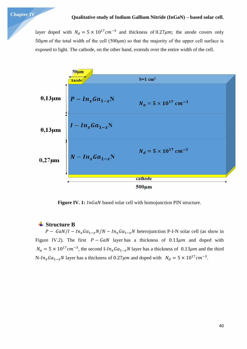
Qualitative study of Indium Gallium Nitride (InGaN) – based solar cell.
40
Chapter IV
layer doped with 𝑁𝑑 = 5 × 10¹⁷𝑐𝑚−3 and thickness of 0.27𝜇𝑚; the anode covers only
50𝜇𝑚 of the total width of the cell (500μm) so that the majority of the upper cell surface is
exposed to light. The cathode, on the other hand, extends over the entire width of the cell.
Figure IV. 1: 𝐼𝑛𝐺𝑎𝑁 based solar cell with homojunction PIN structure.
Structure B 𝑃 − 𝐺𝑎𝑁/𝐼 − 𝐼𝑛𝑥𝐺𝑎1−𝑥𝑁/𝑁 − 𝐼𝑛𝑥𝐺𝑎1−𝑥𝑁 heterojunction P-I-N solar cell (as show in
Figure IV.2). The first 𝑃 − 𝐺𝑎𝑁 layer has a thickness of 0.13𝜇𝑚 and doped with
𝑁𝑎 = 5 × 10¹⁷𝑐𝑚−3, the second I-𝐼𝑛𝑥𝐺𝑎1−𝑥𝑁 layer has a thickness of 0.13𝜇𝑚 and the third
N-𝐼𝑛𝑥𝐺𝑎1−𝑥𝑁 layer has a thickness of 0.27𝜇𝑚 and doped with 𝑁𝑑 = 5 × 10¹⁷𝑐𝑚−3.

Qualitative study of Indium Gallium Nitride (InGaN) – based solar cell.
41
Chapter IV
Figure IV. 2: GaN/InGaN heterojunction solar cell with PIN structure.
Structure C
𝑃 − 𝐺𝑎𝑁/𝐼 − 𝐼𝑛𝑥𝐺𝑎1−𝑥𝑁/𝑁 − 𝐺𝑎𝑁 double heterojunction solar cell with PIN structure
placed on sapphire substrate (see Figure IV.3). The 𝑝 − 𝐺𝑎𝑁 layer has thickness of 0.13𝜇𝑚
and doping𝑁𝑎 = 5 × 10¹⁷𝑐𝑚−3, the I-𝐼𝑛𝑥𝐺𝑎1−𝑥𝑁 layer thickness is 0.13𝜇𝑚 thick, the 𝑁 −
𝐺𝑎𝑁 with thickness of 0.27 𝜇𝑚 and doping 𝑁𝑎 = 5 × 10¹⁷𝑐𝑚−3; the 𝐺𝑎𝑁 buffer layer with
thickness of 2 𝜇𝑚 and sapphire substrate with 20µm of thickness. The anode covers only 50μm
of the total width of the top of the cell so that the majority of the upper cell surface is exposed
to light, the cathode is placed beside them 𝑁 − 𝐺𝑎𝑁 layer.

Qualitative study of Indium Gallium Nitride (InGaN) – based solar cell.
42
Chapter IV
Figure IV. 3: GaN/InGaN double heterojunction solar cell with PIN structure.
The SILVACO-ATLAS presentation of the studied structures of the cell; is illustrated in
the figures (IV.4), (IV.5), (IV.6), (IV.7), (IV.8) and (IV.9) respectively.

Qualitative study of Indium Gallium Nitride (InGaN) – based solar cell.
43
Chapter IV
Figure IV. 4: Structure of InGaN-based homojunction solar cell (structure A) under the
Silvaco-Atlas simulator.
Figure IV. 5: Spatial mesh of the homojunction solar cell (structure A) under the Silvaco-
Atlas simulator.

Qualitative study of Indium Gallium Nitride (InGaN) – based solar cell.
44
Chapter IV
Figure IV. 6: Structure of GaN/InGaN heterojunction solar cell (structure B) under the
Silvaco-Atlas simulator.
Figure IV. 7: Spatial mesh of the heterojunction solar cell (structure B) under the Silvaco-
Atlas simulator.

Qualitative study of Indium Gallium Nitride (InGaN) – based solar cell.
45
Chapter IV
Figure IV. 8: Structure of the GaN/InGaN double heterojunction solar cell (structure C)
under the Silvaco-Atlas simulator.
Figure IV. 9: Spatial mesh of the double heterojunction solar cell (structure C) under the
Silvaco-Atlas simulator.

Qualitative study of Indium Gallium Nitride (InGaN) – based solar cell.
46
Chapter IV
IV.2.2 Input Parameter values
The simulation parameters associated with the studied solar cells are shown in Table IV.1
taking into account the Silvaco database.
Table IV. 1: Simulation parameters associated with the cells studied taking into account the
database of Silvaco data.
Material 𝑰𝒏𝑮𝒂𝑵 𝑮𝒂𝑵 𝑨𝒍𝟐𝑶𝟑
Type Semi-conductor Insulator
The Goal Basic material Optical Windows
collector
Permittivity 𝜺𝒓
𝟏𝟓. 𝟑𝒙 + 𝟖. 𝟗(𝟏 − 𝒙) [43]. 8.9 12
Affinity (ev) 𝟑. 𝟔𝟓𝟗𝐱 − 𝟐. 𝟔𝟔𝟔𝐱𝟐 + 𝟒. 𝟑𝟏 [61]
Band gap 𝑬𝒈 (𝒆𝑽) 𝑬𝒈 (𝒙𝑰𝒏) =3.42x+0.77(1-x)-1.43x (1-x)
[36].
3.42
The effective density
of states for electrons
𝑵𝑪(𝒄𝒎−𝟑)
𝟎. 𝟗 + 𝟐. 𝟑(𝟏 − 𝐱). 𝟏𝟎𝟏𝟖 [62]. 2.24× 𝟏𝟎𝟏𝟖
The effective density
of states for holes
𝑵𝒗(𝒄𝒎−𝟑)
𝟓. 𝟑𝐱 + 𝟏. 𝟖 (𝟏 − 𝐱). 𝟏𝟎𝟏𝟗 [62]. 2.51× 𝟏𝟎𝟏𝟗
Doping(𝒄𝒎−𝟑) 5× 𝟏𝟎𝟏𝟕 𝟓 × 𝟏𝟎𝟏𝟕
The Lifetime(sec)
𝝉𝒏 = 𝝉𝒑
𝟏 × 𝟏𝟎−𝟗 [42]. 𝟔. 𝟓 × 𝟏𝟎−𝟗[63].
Mobility electron
(𝒄𝒎𝟐𝑽−𝟏𝑺−𝟏)
𝟓𝟐𝟒𝒙 + 𝝁𝒏(𝑮𝒂𝑵)[61]. 1000[64].
Mobility hole
(𝒄𝒎−𝟏𝑽−𝟏𝑺−𝟏)
𝟔. 𝟓𝒙 + 𝝁𝒑(𝑮𝒂𝑵)[61]. 350[64].

Qualitative study of Indium Gallium Nitride (InGaN) – based solar cell.
47
Chapter IV
Optical parameters (extinction coefficient k in terms of wavelength 𝜆 for different
concentrations of indium𝑥𝐼𝑛) (see Figure IV.10).
We calculated the extinction coefficient k from the absorption coefficient according to the
following theoretical model 𝛼(𝜆):
𝛼(𝜆) = 𝑎0 √𝑎(𝑥)(𝐸 − 𝐸𝑔) + 𝑏(𝑥)(𝐸 − 𝐸𝑔)2
With: 𝐸 =ℎ𝑐
𝜆 (IV.1)
The dimensionless fitting parameters 𝑎(𝑥) and 𝑏(𝑥) are given for small indium content [40].
For more details and to consider all the indium content compositions, we use further adjustment
parameters 𝑎𝑓𝑖𝑡 and 𝑏𝑓𝑖𝑡 [40]. A linear interpolation is used to find the new fitting parameters
over the entire composition range. In this case, the wavelength-dependent absorption coefficient
has been determined for all alloy compositions. The parameters 𝑎𝑓𝑖𝑡 and 𝑏𝑓𝑖𝑡 are given using
this linear interpolation [41]:
afit = 12.87𝑥4 − 37.79𝑥3 + 40.43𝑥2 − 18.35𝑥 + 3.52 (IV.2)
𝑏𝑓𝑖𝑡 = −2.92𝑥2 + 4.05𝑥 − 0.66 (IV.3)
The extinction coefficient 𝑘 is related to the absorption coefficient 𝛼 following the equation:
𝛼 = 4𝜋
𝜆 𝑘 (IV.4)
Then, we can calculate the extinction coefficient 𝑘 required to be added as data file in Silvaco-
Atlas:
𝑘 =𝛼𝜆
4𝜋 (IV.5)
In our simulations, we will use the Adachi model, which is used to calculate the refractive
index of the materials and the equation that represents this model is [43]:
𝑛𝑟(𝜔) = √𝐴 (ℏ𝜔
𝐸𝑔)
−2
{2 − √1 +ℏ𝜔
𝐸𝑔− √1 −
ℏ𝜔
𝐸𝑔} + 𝐵 (IV.6)
Where 𝐸𝑔 is the bandgap, 𝜔 is the optical frequency and A and B are material composition
dependent parameters. For 𝐼𝑛𝑥𝐺𝑎1−𝑥𝑁, the compositional dependence of the A and B
parameters are given by the expressions in Equations II.7 and II.8 respectively[43].

Qualitative study of Indium Gallium Nitride (InGaN) – based solar cell.
48
Chapter IV
𝐴(𝑥) = 9.827(1 + 𝑥) − 53.57𝑥 (IV.7)
𝐵(𝑥) = 2.736(1 − 𝑥) − 9.19𝑥 (IV.8)
Figure IV. 10: Extinction coefficient k in terms of wavelength 𝜆 for different concentrations
of indium 𝑥𝐼𝑛 according to theoretical calculations[40, 41].
IV.3 Results and discussions
Figure IV.11 shows the energy gap profile of the three studied cells at thermal equilibrium.
The alignment between the two quasi Fermi levels, 𝐸𝑓𝑛 for the electrons and 𝐸𝑓𝑝 for holes, is
well verified at thermal equilibrium for the three cells. In structures B and C, the discontinuity
in 𝐸𝐶 or𝐸𝑉, at GaN/InGaN interfaces, can form a considerable barrier against electron and hole
transport within the i-layer when the InGaN band gap width is reduced enough, and this case
deteriorates considerably the cell performances. For this reason, the InGaN band gap should be
tuned carefully taking into account the discontinuity value in 𝐸𝐶 or 𝐸𝑉 at GaN/InGaN interfaces.
As the InGaN band gap becomes wider, the discontinuity effect is reduced remarkably.
0,0 0,2 0,4 0,6 0,8 1,0 1,2 1,4
0,0
0,1
0,2
0,3
0,4
0,5
0,6
0,7
0,8
Ex
tin
ctio
n c
oef
fici
ent
(k)
(m)
0
0.10
0.15
0.18
0.20
0.24
0.30
0.34
0.40
0.45
0.50
0.52
0.57
0.60
0.65
0.70

Qualitative study of Indium Gallium Nitride (InGaN) – based solar cell.
49
Chapter IV
Figure IV. 11: Energy gap profile of the three studied cells at thermal equilibrium:
(a) structure A, (b) structure B and (c) structure C.
Figures IV.12 present, respectively, the current density - voltage (𝐽 − 𝑉) and the power -
voltage (P-V) electrical characteristics corresponding to the three studied cells A, B and C with
in molar fractions of 𝑥𝐼𝑛=0.24 , 𝑥𝐼𝑛 = 0.34 𝑎𝑛𝑑 𝑥𝐼𝑛 = 0.57 .
0,0 0,1 0,2 0,3 0,4 0,5
-2,0
-1,5
-1,0
-0,5
0,0
0,5
1,0
1,5
2,0
En
ergy (
eV)
x (m)
Efn
Efp
Ev
Ec
0,0 0,1 0,2 0,3 0,4 0,5
-2,0
-1,5
-1,0
-0,5
0,0
0,5
1,0
1,5
2,0
2,5
3,0
3,5 Efn
Efp
Ev
Ec
En
ergy (
eV)
x (m)
0,0 0,1 0,2 0,3 0,4 0,5 0,6 0,7-4
-3
-2
-1
0
1
2
3
4 Efn
Efp
Ev
Ec
En
erg
y (
eV)
x (m)
a)a) b)
c)

Qualitative study of Indium Gallium Nitride (InGaN) – based solar cell.
50
Chapter IV
Figure IV. 12: Current density - voltage (𝐽 − 𝑉) electrical characteristics of the studied solar
cells A, B and C with 𝑥𝐼𝑛=0.24 , 𝑥𝐼𝑛 = 0.34 𝑎𝑛𝑑 𝑥𝐼𝑛 = 0.57, under AM1.5 illumination.
0,0 0,2 0,4 0,6 0,8 1,0 1,2 1,4 1,6 1,8 2,0 2,2 2,4
-2
0
2
4
6
Cu
rren
t d
ensi
ty (
mA
/cm
2)
Voltage (Volt)
A
B
C
xIn
= 0.24
0,0 0,2 0,4 0,6 0,8 1,0 1,2 1,4 1,6 1,8 2,0
-2
0
2
4
6
8
10
Cu
rren
t d
en
sity
(m
A/c
m2
)
Voltage (Volt)
A
B
C
xIn
= 0.34
0,0 0,2 0,4 0,6 0,8 1,0 1,2 1,4 1,6 1,8 2,0
-2
0
2
4
6
8
10
12
14
16
18
20
22
24
Cu
rren
t d
en
sity
(m
A/c
m2
)
Voltage (Volt)
A
B
C
xIn
= 0.57

Qualitative study of Indium Gallium Nitride (InGaN) – based solar cell.
51
Chapter IV
Figure IV. 13: Power - voltage (𝑃 − 𝑉) characteristics of the studied solar cells A, B and C
with 𝑥𝐼𝑛=0.24 , 𝑥𝐼𝑛 = 0.34 𝑎𝑛𝑑 𝑥𝐼𝑛 = 0.57, under AM1.5 illumination.
Table IV.2 presents all results of the cell output parameters (the short-circuit current density
(𝐽𝑠𝑐), the open-circuit voltage (𝑉𝑜𝑐), the fill factor (𝐹𝐹), and the conversion efficiency (𝜂))
obtained by changing 𝑥𝐼𝑛 for each cell structure: A, B and C. In addition, figures IV.14 plots
the cell output parameters variation for the structures A, B and C when indium molar fraction
𝑥𝐼𝑛 is changed.
0,0 0,2 0,4 0,6 0,8 1,0 1,2 1,4 1,6 1,8 2,0 2,2 2,40,000
0,001
0,002
0,003
0,004
0,005
0,006
0,007
0,008
0,009
0,010x
In= 0.24
Pow
er d
ensi
ty (
Watt
/cm
2)
Voltage (Volt)
A
B
C
0,0 0,2 0,4 0,6 0,8 1,0 1,2 1,4 1,6 1,8 2,00,000
0,001
0,002
0,003
0,004
0,005
0,006
0,007
0,008
0,009
0,010
0,011
0,012
0,013
0,014
xIn
= 0.34
Pow
er d
ensi
ty (
Wa
tt/c
m2)
Voltage (Volt)
A
B
C
0,0 0,2 0,4 0,6 0,8 1,0 1,2 1,4 1,6 1,80,000
0,005
0,010
0,015
0,020
0,025
xIn
= 0.57
Pow
er d
ensi
ty (
Wa
tt/c
m2)
Voltage (Volt)
A
B
C

Qualitative study of Indium Gallium Nitride (InGaN) – based solar cell.
52
Chapter IV
Table IV. 2: Cell output parameters variation for the structures A, B and C with changing the
indium molar fraction𝑥𝐼𝑛
Cellule 𝑥𝐼𝑛 𝐽𝑠𝑐
(mA/cm2)
𝑉𝑜𝑐
(Volt)
𝐹𝐹
(%)
𝑃𝑚
(Watt/cm2)
𝜂
(%)
A 0.10 1.41627 2.45824 93.0326 0.00323896 3.23896
0.15 2.38118 2.28733 92.6103 0.00504406 5.04406
0.18 3.12931 2.18711 92.3060 0.00631756 6.31756
0.20 3.63954 2.12116 92.1060 0.00711063 7.11063
0.24 4.88716 1.99203 91.6343 0.00892094 8.92094
0.30 7.00157 1.80485 90.7699 0.01147040 11.4704
0.34 8.65157 1.68522 90.0198 0.01312470 13.1247
0.40 11.5430 1.51376 88.5366 0.01547030 15.4703
0.45 14.3996 1.37859 86.8106 0.01723290 17.2329
0.50 17.6315 1.25021 84.5871 0.01864560 18.6456
0.52 18.9294 1.20063 83.6029 0.01900060 19.0006
0.57 22.4466 1.08162 80.6048 0.01956980 19.5698
0.60 24.6807 1.01358 78.4650 0.01962870 19.6287
0.65 28.5985 0.906162 74.3280 0.01926200 19.262
0.70 31.6987 0.805268 70.0589 0.01788320 17.8832
B 0.10 1.31183 2.47546 92.5552 0.003005620 3.00562
0.15 2.1619 2.30504 91.9548 0.004582350 4.58235
0.18 2.80484 2.20516 91.5508 0.005662530 5.66253
0.20 3.25072 2.13967 91.283 0.006349160 6.34916
0.24 4.3206 2.01126 90.6971 0.007881440 7.88144
0.30 6.14569 1.82559 89.4905 0.010040400 10.0404
0.34 7.56235 1.70845 82.2832 0.010630900 10.6309
0.40 1.80642 1.56214 32.3767 0.000913632 0.913632
0.45 0.440902 1.48604 73.7127 0.000482964 0.482964
0.50 0.353691 1.42396 87.3960 0.000440163 0.440163
0.52 0.349395 1.40056 88.1762 0.000431489 0.431489
0.57 0.347395 1.34341 88.3817 0.000412472 0.412472
0.60 0.347435 1.31103 88.2562 0.000402005 0.402005
0.65 0.347746 1.25936 87.9975 0.000385374 0.385374
C 0.10 0.950938 2.61847 91.4336 0.002276700 2.2767
0.15 1.480410 2.45369 91.1474 0.003310900 3.3109
0.18 1.869640 2.3568 90.8637 0.004003790 4.00379
0.20 2.149100 2.29302 90.6573 0.004467530 4.46753
0.24 2.807150 2.16846 90.1726 0.005488980 5.48898
0.30 3.964970 1.98801 89.1339 0.007025890 7.02589
0.34 4.895900 1.87406 85.5127 0.007845970 7.84597
0.40 1.402380 1.73311 36.718 0.000892422 0.892422
0.45 0.191332 1.66713 45.3088 0.000144524 0.144524
0.50 0.0281717 1.63904 54.2045 2.5028 × 10⁻⁵ 0.0250287
0.52 0.0202431 1.63612 57.3880 1.9007 × 10⁻⁵ 0.019007
0.57 0.0106039 1.63694 78.5582 1.3636 × 10⁻⁵ 0.0136361
0.60 0.00902653 1.63896 81.3945 1.2041 × 10⁻⁵ 0.0120416

Qualitative study of Indium Gallium Nitride (InGaN) – based solar cell.
53
Chapter IV
Figure IV. 14: Solar cell output parameters vs Indium concetraction (𝑥𝐼𝑁) for structures A, B,
and C : a) Short circuit current, b) Open circuit voltage, c) Fill factor and d) Conversion
efficiency .
Somes remarks can be notified from figure IV.14:
❖ The more 𝑥𝐼𝑛 increases, the 𝐽𝑆𝐶 of the cell A increases until reaching a value of
31.6987 mA/cm2 at 𝑥𝐼𝑛 = 0.7, however in cells B and C, 𝐽𝑆𝐶 reaches, respectively, values of
7.5623 mA/cm2 and 4.8959 mA/cm2 at 𝑥𝐼𝑛 = 0.34,and then begins to decrease. The cell A
presents the ideal case, which provides the highest current. The limitations from GaN/InGaN
interfaces in cells B and C, and from GaN/substrate discontinuity in cell C, reduce the current
to a more realist behavior with optimum values at 𝑥𝐼𝑛 = 0.34 corresponding to InGaN band
gap of (2.1981).
0,1 0,2 0,3 0,4 0,5 0,6 0,7
0
5
10
15
20
25
30
35
Jsc
(m
A/c
m2
)
xIn
A
B
C
0,0 0,1 0,2 0,3 0,4 0,5 0,6 0,70,0
0,2
0,4
0,6
0,8
1,0
1,2
1,4
1,6
1,8
2,0
2,2
2,4
2,6
2,8
Vo
c(v
olt
)
A
B
C
xIn
0,1 0,2 0,3 0,4 0,5 0,6 0,7
30
40
50
60
70
80
90
100
FF
(%)
xIn
A
B
C
0,0 0,1 0,2 0,3 0,4 0,5 0,6 0,70,0
2,5
5,0
7,5
10,0
12,5
15,0
17,5
20,0
22,5
A
B
C
Eff
icie
ncy
%
xIn

Qualitative study of Indium Gallium Nitride (InGaN) – based solar cell.
54
Chapter IV
❖ More we increase 𝑥𝐼𝑛, the 𝑉𝑂𝐶 decreases in all structures A, B, and C, because increasing
the molar fraction of in means the reduction of the InGaN band gap, which leads to Voc
diminution.
❖ As 𝑥𝐼𝑛 increases, the fill factor FF decreases in the three structures with the exception
that it reaches a minimum value around 32%-35% for the cells B and C, and then it begin to
increase.
❖ The conversion efficiency increases with increasing indium concentration 𝑥𝐼𝑛 until it
reaches an optimal value of 19.62 % at 𝑥𝐼𝑛 = 0.6 which corresponds to InGaN band gap of (
1.4868)for the ieal case presented by the cell A. Taking into account the GaN/InGaN and
GaN/substrate interface effect lead to more realist conversion efficiency which reaches for cell
C an optimal value of 7.84% at 𝑥𝐼𝑛 = 0.34 corresponding to InGaN band gap of (2.1981). We
notify that 7.84% is in the best efficiency range obtained experimentally [65].
IV.3.1 Effect of defects
We observed from experimental measurements that the lifetime of 𝐼𝑛𝐺𝑎𝑁 changes within
the range [10−9 − 10−6 𝑠𝑒𝑐] [42]. Therefore, the effect of defects can be studied by changing
the lifetime values of electrons (𝜏𝑛) and holes (𝜏𝑝) within the range obtained experimentally
[42, 63]. This is done by giving 𝜏𝑛 and 𝜏𝑝 the same values listed in Table IV .3 for the cell C
optimized with 𝑥𝐼𝑛 = 0.34 . When activating the SRH model and inserting 𝜏𝑛 and 𝜏𝑝values,
Silvaco uses the simplest model of defects, which is presented, by single recombination center
level in the middle of the band gap.
An increase of 𝜏𝑛 and 𝜏𝑝 values means a decrease in the defects concentration 𝑁𝑅 (𝑐𝑚−3)
following equations IV.9-IV.11:
𝜏𝑛 =1
𝐶𝑛𝑁𝑅 (IV.9)
𝜏𝑝 =1
𝐶𝑝𝑁𝑅 (IV.10)
Where 𝐶𝑃 𝑎𝑛𝑑 𝐶𝑛hole and electron are capture coefficients respectively (𝑐𝑚 3. 𝑠𝑒𝑐−1).
The value of 𝑁𝑅 is then deduced:
𝑁𝑅 =1
𝐶𝑛𝜏𝑛 (IV.11)

Qualitative study of Indium Gallium Nitride (InGaN) – based solar cell.
55
Chapter IV
The value of 𝐶𝑛 can be calculated from Silvaco manuel which give 𝜏𝑛 = 10−7𝑠𝑒𝑐 for
𝑁𝑅 =5×10¹⁶𝑐𝑚−3[43] then :
𝐶𝑛 =1
𝜏𝑛𝑁𝑅=
1
10−7×5×1016 = 2 × 10⁻¹⁰ 𝑐𝑚 3. 𝑠𝑒𝑐−1 .
𝑁𝑅 Corresponding to 𝜏𝑛 = 10−9𝑠𝑒𝑐 be then:
𝑁𝑅 =1
2×10−10×10−9 = 5 × 10¹⁸𝑐𝑚−3.
Table IV. 3: Lifetime effect on the output parameters (𝐽𝑆𝐶 , 𝑉𝑂𝐶 , 𝐹𝐹, 𝑃𝑚𝑎𝑥, 𝑎𝑛𝑑 𝜂 ) of the cell
C optimized with 𝑥𝐼𝑛 = 0.34.
Cell C
𝑥𝐼𝑛=0.34
𝐽𝑠𝑐
(mA/cm2)
𝑉𝑜𝑐 (Volt)
𝐹𝐹 (%)
𝑃𝑚
(Watt/cm2)
𝜂 (%)
𝜏𝑛(sec)
𝑁𝑅(𝑐𝑚−3)
1 × 10⁻⁹ 4.89565 1.57979 81.8165 0.00632777 6.32777
5 × 10¹⁸
5 × 10⁻⁹ 4.89585 1.65288 82.7531 0.00669659 6.69659
1 × 10¹⁸
1 × 10⁻⁸ 4.89588 1.68361 83.1373 0.0068528 6.85280
5 × 10¹⁷
5 × 10⁻⁸ 4.89590 1.75283 84.0105 0.00720951 7.20951
1 × 10¹⁷
1 × 10⁻⁷ 4.89590 1.78165 84.3804 0.00736032 7.36032
5 × 10¹⁶
5 × 10⁻⁷ 4.89590 1.84648 85.2051 0.0077027 7.70270
1 × 10¹⁶
1 × 10⁻⁶ 4.89590 1.87406 85.5127 0.00784597 7.84597
5 × 10¹⁵
5 × 10⁻⁶ 4.89590 1.94078 85.9674 0.00816851 8.16851
1 × 10¹⁵
Figures IV.15- IV.18 show the lifetime (and the corresponding𝑁𝑅) effects on the output
parameters (𝐽𝑆𝐶 , 𝑉𝑂𝐶 , 𝐹𝐹, 𝑎𝑛𝑑 𝜂 ) of the cell C optimized with 𝑥𝐼𝑛 = 0.34.

Qualitative study of Indium Gallium Nitride (InGaN) – based solar cell.
56
Chapter IV
Figure IV. 15: Lifetime (and the corresponding𝑁𝑅) effects on the 𝐽𝑆𝐶 of the cell C optimized
with 𝑥𝐼𝑛 = 0.34.
❖ 𝐽𝑆𝐶 Shows a slight increase as the lifetime 𝜏𝑛 increases corresponding to a defect
concentration decrease.
❖ 𝜏𝑛 > 5 × 10⁻⁸𝑠 The current density 𝐽𝑆𝐶 becomes insensitive to further 𝜏𝑛 increase.
Figure IV. 16: Lifetime (and the corresponding𝑁𝑅) effects on the 𝑉𝑜𝑐 of the cell C optimized
with 𝑥𝐼𝑛 = 0.34.
The 𝑉𝑂𝐶 however shows a discernible dependency on 𝜏𝑛 (and its corresponding 𝑁𝑅). The
more we increase 𝜏𝑛 the greater is the𝑉𝑂𝐶, and this can be explained via the diffusion length L.
Following equation IV.12, 𝜏𝑛 increase leads to diffusion length L increase:
1015
1016
1017
1018
1019
4,89565
4,89570
4,89575
4,89580
4,89585
4,89590
JS
C(m
A/c
m2
)
NR(cm-3
)
xIn
=0.34
10-9
10-8
10-7
10-6
10-5
4,8956
4,8957
4,8958
4,8959
J
SC
(mA
/cm
2)
n(sec)
xIn
=0.34
10-9
10-8
10-7
10-6
1,55
1,60
1,65
1,70
1,75
1,80
1,85
1,90
1,95
Voc(
Volt
)
n(sec)
XIn=0.34
1015
1016
1017
1018
1019
1,55
1,60
1,65
1,70
1,75
1,80
1,85
1,90
1,95
Voc(
Volt
)
NR(cm-3
)
XIn=0.34

Qualitative study of Indium Gallium Nitride (InGaN) – based solar cell.
57
Chapter IV
𝐿 = √𝐷𝜏𝑛 (IV.12)
Where D the carrier diffusivity.
In addition, L increase leads to the saturation current 𝐽0decrease following equation IV.13:
𝐽0 = 𝑞. 𝑛𝑖2 (
𝐷𝑛
𝐿𝐷𝑁𝐴+
𝐷𝑃
𝐿𝑃𝑁𝐷) (IV.13)
Decrease of 𝐽0 leads to the increased 𝑉𝑂𝐶 following the equation IV.3:
𝑉𝑂𝐶 =𝑘𝛽𝑇
𝑞𝑙𝑛 (
𝐽𝑆𝐶
𝐽0+ 1) (IV.14)
We can say that the 𝜏𝑛 increase leads to an increase in L and hence a decrease in 𝐽0 and this
leads to an increase in 𝑉𝑂𝐶 .
Figure IV. 17: Lifetime (and the corresponding𝑁𝑅) effects on the 𝐹𝐹 of the cell C optimized
with 𝑥𝐼𝑛 = 0.34.
It is clear that a lifetime 𝜏𝑛 increase (which corresponds to 𝑁𝑅 decrease) will enhance
remarkably the fill factor FF.
10-9
10-8
10-7
10-6
10-5
81
82
83
84
85
86
FF
(%)
n(sec)
xIn=0.34
1015
1016
1017
1018
81
82
83
84
85
86
FF
(%)
NR(cm-3
)
xIn
=0.34

Qualitative study of Indium Gallium Nitride (InGaN) – based solar cell.
58
Chapter IV
Figure IV. 18: Lifetime (and the corresponding 𝑁𝑅) effects on the conversion efficiency of
the cell C optimized with 𝑥𝐼𝑛 = 0.34.
The considerable improvement of 𝑉𝑂𝐶 and FF as the lifetime 𝜏𝑛 increases (or the 𝑁𝑅 decreases)
will lead to a considerable improvement of the conversion efficiency as shown in figure IV.18.
IV.3.2 Effect of 𝑷 – 𝑮𝒂𝑵 layer thickness
The effect of 𝑃 − 𝐺𝑎𝑁 layer thickness on solar cell output parameters of the PIN
GaN/InGaN double heterojunction solar cell (cell C) is shown in Table IV.4 and on Figure
IV.20. The 𝑃 − 𝐺𝑎𝑁 layer thickness is varied from 50 to 270 nm.
10-9
10-8
10-7
10-6
10-5
6,0
6,5
7,0
7,5
8,0
8,5
Eff
icie
ncy
(%)
n(sec)
xIn=0.34
1015
1016
1017
1018
81
82
83
84
85
86
FF
(%)
NR(cm-3
)
xIn
=0.34

Qualitative study of Indium Gallium Nitride (InGaN) – based solar cell.
59
Chapter IV
Table IV. 4: 𝑃 − 𝐺𝑎𝑁 layer thickness effect on the output parameters of the cell C optimized
with 𝑥𝐼𝑛 = 0.34.
Cell C
𝒙𝑰𝒏=0.34
𝑷 − 𝑮𝒂𝑵 𝒕𝒉𝒊𝒄𝒌𝒏𝒆𝒔𝒔
(nm)
𝑱𝒔𝒄
(mA/cm2)
𝑽𝒐𝒄
(Volt)
𝑭𝑭
(%)
𝑷𝒎
(Watt/cm2)
𝜼
(%)
50 4.89929 1.87344 80.2110 0.00736219 7.36219
60 4.89930 1.87354 82.5956 0.00758148 7.58148
70 4.89919 1.87364 83.6980 0.00768291 7.68291
80 4.89892 1.87372 84.3130 0.00773926 7.73926
90 4.89855 1.87380 84.7100 0.00777545 7.77545
100 4.89806 1.87388 85.0015 0.00780176 7.80176
110 4.89746 1.87394 85.2096 0.00782015 7.82015
120 4.89675 1.87400 85.3708 0.00783406 7.83406
130 4.89590 1.87406 85.5127 0.007845970 7.84597
140 4.89494 1.8741 85.6241 0.00785482 7.85482
150 4.89384 1.87414 85.7141 0.00786148 7.86148
160 4.89262 1.87418 85.7888 0.00786653 7.86653
170 4.89126 1.87421 85.8511 0.00787018 7.87018
180 4.88978 1.87423 85.9137 0.00787362 7.87362
190 4.88816 1.87425 85.9703 0.00787628 7.87628
200 4.88640 1.87427 86.0195 0.00787804 7.87804
210 4.88452 1.87428 86.0628 0.00787901 7.87901
220 4.88251 1.87429 86.1014 0.00787935 7.87935
230 4.88037 1.87429 86.1359 0.00787905 7.87905
240 4.87810 1.87429 86.1668 0.00787821 7.87821
250 4.87571 1.87429 86.1949 0.00787692 7.87692
260 4.87319 1.87428 86.2204 0.00787513 7.87513
270 4.87056 1.87427 86.2435 0.00787295 7.87295

Qualitative study of Indium Gallium Nitride (InGaN) – based solar cell.
60
Chapter IV
Figure IV. 19: Solar cell output parameters vs 𝑃 − 𝐺𝑎𝑁 thickness for cell C: a)𝐽𝑠𝑐, b)𝑉𝑜𝑐, c)
FF and d) Efficiency.
A slight decrease can be notified in the short circuit current density 𝐽𝑠𝑐 as the 𝑃 − 𝐺𝑎𝑁 layer
thickness increases, while the Voc shows a slight increase. The FF and efficiency show however
a discernible improvement.
IV.3.3 Effect of 𝑰 – 𝑰𝒏𝑮𝒂𝑵 layer thickness
The effect of 𝐼 – 𝐼𝑛𝐺𝑎𝑁 layer thickness on solar cell output parameters of the PIN
GaN/InGaN double heterojunction solar cell (cell C) is shown in Table IV.5 and on Figure
IV.20. The 𝐼 – 𝐼𝑛𝐺𝑎𝑁 layer thickness is varied from 50 to 850 nm.
50 100 150 200 2504,870
4,875
4,880
4,885
4,890
4,895
4,900
JS
C(m
A/c
m2)
P-GaN thickness (nm)
xIn
=0.34
50 100 150 200 250
1,8734
1,8736
1,8738
1,8740
1,8742
1,8744
Vo
c(V
olt
)
P-GaN thickness(nm)
XIn
=0.34
50 100 150 200 250
80
81
82
83
84
85
86
87
FF
(%)
P-GaN thickness (nm)
xIn
=0.34
50 100 150 200 2507,3
7,4
7,5
7,6
7,7
7,8
7,9
Eff
icie
ncy
(%)
P-GaN thickness(nm)
xIn
=0.34

Qualitative study of Indium Gallium Nitride (InGaN) – based solar cell.
61
Chapter IV
Table IV. 5: 𝐼 − 𝐼𝑛𝐺𝑎𝑁 layer thickness effect on the output parameters of the cell C
optimized with 𝑥𝐼𝑛 = 0.34.
Cell C
𝒙𝑰𝒏=0.34
𝑰 − 𝑰𝒏𝑮𝒂𝑵
𝒕𝒉𝒊𝒄𝒌𝒏𝒆𝒔𝒔
(nm)
𝑱𝒔𝒄
(mA/cm2)
𝑽𝒐𝒄
(Volt)
𝑭𝑭
(%)
𝑷𝒎
(Watt/cm2)
𝜼
(%)
50 2.67298 1.90847 87.1017 0.00444332 4.44332
100 4.20240 1.88417 86.3573 0.00683780 6.83780
150 5.28845 1.86835 84.9033 0.00838902 8.38902
200 6.08195 1.85627 83.309 0.00940537 9.40537
250 6.67563 1.84648 81.7091 0.01007180 10.0718
300 7.12889 1.83821 80.2425 0.01051530 10.5153
350 7.48114 1.83102 78.9984 0.01082130 10.8213
400 7.75930 1.82459 77.9811 0.01104020 11.0402
450 7.98217 1.81891 77.1342 0.01119900 11.1990
500 8.16313 1.81366 76.4343 0.01131620 11.3162
550 8.31183 1.80894 75.8427 0.01140340 11.4034
600 8.43542 1.80449 75.3487 0.01146930 11.4693
650 8.53921 1.80047 74.9191 0.0115185 11.5185
700 8.62719 1.79661 74.5486 0.0115548 11.5548
750 8.70246 1.79304 74.2239 0.0115818 11.5818
800 8.76735 1.78975 73.9368 0.0116017 11.6017
850 8.82374 1.78652 73.6885 0.0116161 11.6161

Qualitative study of Indium Gallium Nitride (InGaN) – based solar cell.
62
Chapter IV
Figure IV. 20: Solar cell output parameters vs 𝐼 − 𝐼𝑛𝐺𝑎𝑁 thickness for cell C: a)𝐽𝑠𝑐, b)𝑉𝑜𝑐, c)
FF and d) Efficiency.
❖ The 𝐽𝑆𝐶 increases as the 𝐼 − 𝐼𝑛𝐺𝑎𝑁 layer thickness increases and this can be explained
by the photons, which get longer path for absorption, and unabsorbed lower energy photons
from 𝑝 − 𝐺𝑎𝑁 layer get absorbed in this region. Photon absorption is also supported by higher
absorption coefficient of 𝐼𝑛𝐺𝑎𝑁 material.
❖ The decrease in 𝑉𝑂𝐶 value as 𝐼 − 𝐼𝑛𝐺𝑎𝑁 layer increases by the fact that higher thickness
generates more carriers and recombination, resulting in decreased open circuit voltage.
❖ The fill factor FF starts decreasing with respect to increased 𝐼 − 𝐼𝑛𝐺𝑎𝑁 thickness
because the series resistance increases with increasing 𝐼 − 𝐼𝑛𝐺𝑎𝑁 thickness.
❖ The efficiency 𝜂 increases as the 𝐼 − 𝐼𝑛𝐺𝑎𝑁 layer thickness increases and this can be
explained by the fact that efficiency η follows the current density 𝐽𝑆𝐶because the latter is the
predominant and directly influencing factor.
0 100 200 300 400 500 600 700 800 9002
3
4
5
6
7
8
9
JS
C(m
A/c
m2)
i-InGaN thickness (nm)
xIn
=0.34
0 100 200 300 400 500 600 700 800 9001,78
1,80
1,82
1,84
1,86
1,88
1,90
1,92
Voc(
Volt
)
i-InGaN thickness(nm)
XIn
=0.34
0 100 200 300 400 500 600 700 800 90072
74
76
78
80
82
84
86
88
FF
(%)
i-InGaN thickness (nm)
xIn
=0.34
0 100 200 300 400 500 600 700 800 9004
5
6
7
8
9
10
11
12
Eff
icie
ncy
(%)
i-InGaN thickness(nm)
xIn
=0.34

Qualitative study of Indium Gallium Nitride (InGaN) – based solar cell.
63
Chapter IV
IV.4 Conclusion
In this last chapter, we studied three InGaN-based PIN solar cell with the following
structures: structure A which is a single InGaN homojunction, structure B which is GaN/InGaN
heterojunction and structure C, which is a GaN/InGaN double heterojunction with GaN buffer
layer on sapphire substrate. The three cells were investigated under solar radiation (AM1.5) and
along with a wide energy range (by changing the molar fraction of indium 𝑥𝐼𝑛). The study was
carried out using the Silvaco-Atlas software simulator. The latter allowed us to calculate the
electric characteristics of the cell as the current density -voltage (J-V), and the power- voltage
(P-V) characteristics, and the photovoltaic parameters related to these characteristics such as
the short-circuit current density (𝐽𝑠𝑐), the open-circuit voltage (𝑉𝑜𝑐); the maximum power
(𝑃𝑚𝑎𝑥) delivered by the cell, the fill factor (𝐹𝐹), and the conversion efficiency (𝜂). The largest
efficiency is provided by the single homojunction solar cell (structure A) which gave 19.62%
with (𝐼𝑛0.60𝐺𝑎0.40𝑁) alloy. The better efficiency reached by the GaN/InGaN heterojunction
solar cell (structure B) is 10.63% with (𝐼𝑛0.34𝐺𝑎0.66𝑁) alloy. The GaN/InGaN double
heterojunction (structure C) gave an optimal efficiency of 7.84% with (𝐼𝑛0.34𝐺𝑎0.66𝑁) alloy.
Further improvement of the structure C efficiency was achieved by the lifetime 𝜏𝑛 effect, which
gave an optimal efficiency of 8.16%, by the 𝑃 − 𝐺𝑎𝑁 layer thickness effect, which gave an
optimal efficiency of 7.87%, and by the 𝐼 − 𝐼𝑛𝐺𝑎𝑁 layer thickness effect, which gave an
optimal efficiency of 11.61%.

General conclusion

𝐼𝑛𝐺𝑎𝑁 alloy semiconductor materials have the potential to make a major breakthrough in
the photovoltaic industry. Indeed these materials possess unique characteristics to achieve solar
cells with very high efficiency of conversion and low cost: very high absorption coefficient
across the spectrum solar energy, high mobilities, relatively low effective masses, an electronic
gap which scans the entire visible spectrum, from the near infrared (𝐼𝑛𝑁 gap = 0.77 eV) to
ultraviolet (𝐺𝑎𝑁 gap = 3.4 eV), very high resistance to radiation and other extreme conditions.
Despite this, 𝐼𝑛𝐺𝑎𝑁-based cells really did not reach the expected efficiency due to
manufacturing, design and other problems.
In this work, we studied three InGaN-based PIN solar cell with the following structures:
structure A which is a single InGaN homojunction, structure B which is GaN/InGaN
heterojunction and structure C, which is a GaN/InGaN double heterojunction with GaN buffer
layer on sapphire substrate. The three cells were investigated under solar radiation (AM1.5) and
along with a wide energy range (by changing the molar fraction of indium 𝑥𝐼𝑛). The study was
carried out using the Silvaco-Atlas software simulator. The latter allowed us to calculate the
electric characteristics of the cell as the current density -voltage (J-V), and the power- voltage
(P-V) characteristics, and the photovoltaic parameters related to these characteristics such as
the short-circuit current density (𝐽𝑠𝑐), the open-circuit voltage (𝑉𝑜𝑐); the maximum power
(𝑃𝑚𝑎𝑥) delivered by the cell, the fill factor (𝐹𝐹), and the conversion efficiency (𝜂). The largest
efficiency is provided by the single homojunction solar cell (structure A) which gave 19.62%
with (𝐼𝑛0.60𝐺𝑎0.40𝑁) alloy. The better efficiency reached by the GaN/InGaN heterojunction
solar cell (structure B) is 10.63% with (𝐼𝑛0.34𝐺𝑎0.66𝑁) alloy. The GaN/InGaN double
heterojunction (structure C) gave an optimal efficiency of 7.84% with (𝐼𝑛0.34𝐺𝑎0.66𝑁) alloy.
Further improvement of the structure C efficiency was achieved by the lifetime 𝜏𝑛 effect, which
gave an optimal efficiency of 8.16%, by the 𝑃 − 𝐺𝑎𝑁 layer thickness effect, which gave an
optimal efficiency of 7.87%, and by the 𝐼 − 𝐼𝑛𝐺𝑎𝑁 layer thickness effect, which gave an
optimal efficiency of 11.61%.
[1] A. Mahfoud, "Modélisation des cellules solaires tandem à couches minces et à haut
rendement," 2018.
[2] https://venturesolar.com/the-importance-of-solar-energy/.
[3] M. Grätzel, "Photoelectrochemical cells," nature, vol. 414, p. 338, 2001.
[4] A. G. Bhuiyan, K. Sugita, A. Hashimoto, and A. Yamamoto, "InGaN solar cells: present
state of the art and important challenges," IEEE Journal of photovoltaics, vol. 2, pp.
276-293, 2012.
[5] J. Tang, "From Silicon to Germanium Nanowires: growth processes and solar cell
structures," Université Paris-Saclay, 2017.
[6] A. M. Bagher, M. M. A. Vahid, and M. Mohsen, "Types of solar cells and application,"
American Journal of optics and Photonics, vol. 3, pp. 94-113, 2015.
[7] R. K. Pachauri, M. R. Allen, V. R. Barros, J. Broome, W. Cramer, R. Christ, J. A.
Church, L. Clarke, Q. Dahe, and P. Dasgupta, Climate change 2014: synthesis report.
Contribution of Working Groups I, II and III to the fifth assessment report of the
Intergovernmental Panel on Climate Change: IPCC, 2014.
[8] L. M. Fraas and L. D. Partain, Solar cells and their applications vol. 236: John Wiley
& Sons, 2010.
[9] L. M. Fraas, "History of solar cell development," in Low-Cost Solar Electric Power, ed:
Springer, 2014, pp. 1-12.
[10] A. Piebalgs and J. Potocnik, "Photovoltaic Solar Energy Development and Current
Research," European Communities, ISBN 978-92-79-10644, vol. 6, 2009.
[11] A. BENMIR, "Simulation d'une cellule solaire photovoltaïque en couche mince à
hétérojonction: CdS/CIGS et CdS/CZTS."
[12] https://www.pveducation.org/pvcdrom/welcome-to-pvcdrom/solar-cell-operation.
[13] D. Vasileska and G. Klimeck, "Solar Cells Operation and Modeling," 2010.
[14] N. Oleksiy, "Simulation, fabrication et analyse de cellules photovoltaïques à contacts
arrières interdigités," Institut national des sciences appliquée de Lyon, 2005.
[15] S. O. Kasap, Principles of electronic materials and devices vol. 2: McGraw-Hill New
York, 2006.
[16] C. Algora, E. Ortiz, I. Rey-Stolle, V. Díaz, R. Peña, V. M. Andreev, V. P. Khvostikov,
and V. D. Rumyantsev, "A GaAs solar cell with an efficiency of 26.2% at 1000 suns
and 25.0% at 2000 suns," IEEE Transactions on Electron Devices, vol. 48, pp. 840-844,
2001.
[17] A. Blakers, N. Zin, K. R. McIntosh, and K. Fong, "High efficiency silicon solar cells,"
Energy Procedia, vol. 33, pp. 1-10, 2013.
[18] M. Powalla, S. Paetel, D. Hariskos, R. Wuerz, F. Kessler, P. Lechner, W. Wischmann,
and T. M. Friedlmeier, "Advances in cost-efficient thin-film photovoltaics based on Cu
(In, Ga) Se2," Engineering, vol. 3, pp. 445-451, 2017.
[19] S. Moon, K. Kim, Y. Kim, J. Heo, and J. Lee, "Highly efficient single-junction GaAs
thin-film solar cell on flexible substrate," Scientific reports, vol. 6, p. 30107, 2016.
[20] S. Nakamura, M. Senoh, and T. Mukai, "Highly p-typed Mg-doped GaN films grown
with GaN buffer layers," Japanese journal of applied physics, vol. 30, p. L1708, 1991.
[21] C. Himwas, "III-Nitride nanostructures for UV emitters," Université Grenoble Alpes,
2015.
[22] L. Hsu and W. Walukiewicz, "Modeling of InGaN/Si tandem solar cells," Journal of
Applied Physics, vol. 104, p. 024507, 2008.

[23] M. Higashiwaki, T. Inushima, and T. Matsui, "Control of electron density in InN by Si
doping and optical properties of Si‐doped InN," physica status solidi (b), vol. 240, pp.
417-420, 2003.
[24] D. McLaughlin, "Optical Characterization of Indium Gallium Nitride for Application in
High-Efficiency Solar Photovoltaic Cells," 2011.
[25] M. Anani, H. Abid, Z. Chama, C. Mathieu, A. Sayede, and B. Khelifa, "InxGa1− xN
refractive index calculations," Microelectronics Journal, vol. 38, pp. 262-266, 2007.
[26] Q. A. H. Al-Naser, H. W. Hilou, and A. F. Abdulkader, "The last development in III-V
multi-junction solar cells," in 2009 ISECS International Colloquium on Computing,
Communication, Control, and Management, 2009, pp. 373-378.
[27] V. Y. Davydov, A. Klochikhin, V. V. Emtsev, D. Kurdyukov, S. Ivanov, V. Vekshin,
F. Bechstedt, J. Furthmüller, J. Aderhold, and J. Graul, "Band gap of hexagonal InN and
InGaN alloys," physica status solidi (b), vol. 234, pp. 787-795, 2002.
[28] Y. Sato and S. Sato, "Growth and some properties of Inx Ga1− x N thin films by reactive
evaporation," Thin Solid Films, vol. 261, pp. 87-89, 1995.
[29] O. Jani, I. Ferguson, C. Honsberg, and S. Kurtz, "Design and characterization of Ga N∕
In Ga N solar cells," Applied Physics Letters, vol. 91, p. 132117, 2007.
[30] Y. Nanishi, Y. Saito, and T. Yamaguchi, "RF-molecular beam epitaxy growth and
properties of InN and related alloys," Japanese journal of applied physics, vol. 42, p.
2549, 2003.
[31] R. Dahal, B. Pantha, J. Li, J. Lin, and H. Jiang, "InGaN/GaN multiple quantum well
solar cells with long operating wavelengths," Applied Physics Letters, vol. 94, p.
063505, 2009.
[32] M. Yamaguchi, T. Takamoto, and K. Araki, "Super high-efficiency multi-junction and
concentrator solar cells," Solar energy materials and solar cells, vol. 90, pp. 3068-3077,
2006.
[33] F. Yam and Z. Hassan, "InGaN: An overview of the growth kinetics, physical properties
and emission mechanisms," Superlattices and Microstructures, vol. 43, pp. 1-23, 2008.
[34] T. Takeuchi, H. Takeuchi, S. Sota, H. Sakai, H. Amano, and I. Akasaki, "Optical
properties of strained AlGaN and GaInN on GaN," Japanese journal of applied physics,
vol. 36, p. L177, 1997.
[35] P. Schley, R. Goldhahn, A. Winzer, G. Gobsch, V. Cimalla, O. Ambacher, H. Lu, W.
Schaff, M. Kurouchi, and Y. Nanishi, "Dielectric function and Van Hove singularities
for In-rich In x Ga 1− x N alloys: Comparison of N-and metal-face materials," Physical
Review B, vol. 75, p. 205204, 2007.
[36] J. Wu, W. Walukiewicz, K. M. Yu, J. Ager III, E. Haller, H. Lu, and W. J. Schaff,
"Small band gap bowing in In 1− x Ga x N alloys," Applied Physics Letters, vol. 80, pp.
4741-4743, 2002.
[37] S. Nakamura, "Growth of InxGa (1− x) N compound semiconductors and high-power
InGaN/AlGaN double heterostructure violet-light-emitting diodes," Microelectronics
Journal, vol. 25, pp. 651-659, 1994.
[38] S. Pereira, M. Correia, T. Monteiro, E. Pereira, E. Alves, A. Sequeira, and N. Franco,
"Compositional dependence of the strain-free optical band gap in In x Ga 1− x N layers,"
Applied Physics Letters, vol. 78, pp. 2137-2139, 2001.
[39] W. Shan, W. Walukiewicz, E. Haller, B. Little, J. Song, M. McCluskey, N. Johnson, Z.
Feng, M. Schurman, and R. Stall, "Optical properties of In x Ga 1− x N alloys grown
by metalorganic chemical vapor deposition," Journal of Applied Physics, vol. 84, pp.
4452-4458, 1998.
[40] J. W. A. G.F.Brown, W.Walukiewicz,J.Wu,Sol., "EnergyMater.Sol.Cells94," pp. 478–
483., 2010.

[41] R. Belghouthi, S. Taamalli, F. Echouchene, H. Mejri, and H. Belmabrouk, "Modeling
of polarization charge in N-face InGaN/GaN MQW solar cells," Materials Science in
semiconductor Processing, vol. 40, pp. 424-428, 2015.
[42] G. Brown, J. Ager III, W. Walukiewicz, and J. Wu, "Finite element simulations of
compositionally graded InGaN solar cells," Solar energy materials and solar cells, vol.
94, pp. 478-483, 2010.
[43] P. Henry, Atlas User’s Manual DEVICE SIMULATION SOFTWARE, 2015.
[44] M. Leszczynski, R. Czernecki, S. Krukowski, M. Krysko, G. Targowski, P. Prystawko,
J. Plesiewicz, P. Perlin, and T. Suski, "Indium incorporation into InGaN and InAlN
layers grown by metalorganic vapor phase epitaxy," Journal of Crystal Growth, vol.
318, pp. 496-499, 2011.
[45] M. Gartner, C. Kruse, M. Modreanu, A. Tausendfreund, C. Roder, and D. Hommel,
"Optical characterization of InxGa1− xN alloys," Applied surface science, vol. 253, pp.
254-257, 2006.
[46] C. Parker, J. Roberts, S. Bedair, M. Reed, S. Liu, and N. El-Masry, "Determination of
the critical layer thickness in the InGaN/GaN heterostructures," Applied Physics Letters,
vol. 75, pp. 2776-2778, 1999.
[47] V. Gorge, "Caractérisations de matériaux et tests de composants des cellules solaires à
base des nitrures des éléments III-V," Paris 11, 2012.
[48] K. Iwata, H. Asahi, K. Asami, R. Kuroiwa, and S.-i. Gonda, "Gas source molecular
beam epitaxy growth of GaN on C-, A-, R-and M-plane sapphire and silica glass
substrates," Japanese journal of applied physics, vol. 36, p. L661, 1997.
[49] S. O. Kasap, Principles of electrical engineering materials and devices: McGraw-Hill
Companies, 2000.
[50] M. Adaika, "Effet des défauts sur le fonctionnement d’un transistor couche mince
(TFT): Comparaison entre un TFT en a-Si: H et un TFT en a-IGZO par SILVACO
ATLAS," 2017.
[51] N. Benadla, "Optimisation des émetteurs sélectifs et passivables des cellules solaires
conventionnelles à base de mc_si."
[52] P. Michalopoulos, "A novel approach for the development and optimization of state-of-
the-art photovoltaic devices using Silvaco," NAVAL POSTGRADUATE SCHOOL
MONTEREY CA2002.
[53] W. DIB, "Modélisation des structures photovoltaïques: Aspects fondamentaux et
appliqués," 2011.
[54] https://www.silvaco.com/.
[55] B. Garcia Jr, "Indium gallium nitride multijunction solar cell simulation using silvaco
atlas," NAVAL POSTGRADUATE SCHOOL MONTEREY CA2007.
[56] K. Fotis, "Modeling and simulation of a dual-junction CIGS solar cell using Silvaco
ATLAS," NAVAL POSTGRADUATE SCHOOL MONTEREY CA2012.
[57] Atlas User’s Manual: Device Simulation Software, 2013.
[58] D. Schiavo, "Modeling Radiation Effects on a Triple Junction Solar Cell using Silvaco
ATLAS," NAVAL POSTGRADUATE SCHOOL MONTEREY CA2012.
[59] S. Chala, " قتتصوين و بحث الخلايا الشوسيت ذاث الطبقاث الرقي "II-VI Design and investigate of
II-VI thin film solar cells Conception et investigation des cellules solaires en couches
minces II-VI," UNIVERSITE DE MOHAMED KHIDER BISKRA, 2017.
[60] R. Boumaraf, "Simulation de l’effet de la température et les défauts sur les
caractéristiques électriques des diodes à base de GaAs," Université Mohamed Khider-
Biskra, 2015.
[61] M. Nawaz and A. Ahmad, "A TCAD-based modeling of GaN/InGaN/Si solar cells,"
Semiconductor Science and Technology, vol. 27, p. 035019, 2012.

[62] M. E. Levinshtein, S. L. Rumyantsev, and M. S. Shur, Properties of Advanced
Semiconductor Materials: GaN, AIN, InN, BN, SiC, SiGe: John Wiley & Sons, 2001.
[63] S. Lin, S. Zeng, X. Cai, J. Zhang, S. Wu, L. Sun, and B. Zhang, "Simulation of doping
levels and deep levels in InGaN-based single-junction solar cell," Journal of Materials
Science, vol. 47, pp. 4595-4603, 2012.
[64] http://www.ioffe.ru/SVA/NSM/Semicond/GaN/ebasic.htm.
[65] A. S. Kushwaha, P. Mahala, and C. Dhanavantri, "Optimization of p-GaN/InGaN/n-
GaN double heterojunction pin solar cell for high efficiency: simulation approach,"
International Journal of Photoenergy, vol. 2014, 2014.

In this work, we studied three 𝐼𝑛𝐺𝑎𝑁-based PIN solar cell. The first one is a
single 𝐼𝑛𝐺𝑎𝑁 homojunction (structure A), the second one is a GaN/InGaN
heterojunction (structure B) and the third one is a 𝐺𝑎𝑁/𝐼𝑛𝐺𝑎𝑁 double
heterojunction with GaN buffer layer on sapphire substrate (structure C). The
study was carried out using the Silvaco-Atlas software simulator. The largest
efficiency was provided by the cell A which gave 19.62% with (𝐼𝑛0.60𝐺𝑎0.40𝑁)
alloy. The better efficiency reached by the cell B is 10.63% with (𝐼𝑛0.34𝐺𝑎0.66𝑁)
alloy. The cell C gave an optimal efficiency of 7.84% with (𝐼𝑛0.34𝐺𝑎0.66𝑁) alloy.
Further improvement of the cell C efficiency was achieved by the lifetime 𝜏𝑛
effect, which gave an optimal efficiency of 8.16%, by the 𝑃 − 𝐺𝑎𝑁 layer
thickness effect, which gave an optimal efficiency of 7.87%, and by the 𝐼 −
𝐼𝑛𝐺𝑎𝑁 layer thickness effect, which gave an optimal efficiency of 11.61%.
Key words: InGaN- solar cell- Efficiency -Simulation- Silvaco Atlas.
Dans ce travail, nous avons étudié trois cellules solaires PIN basées sur
𝐼𝑛𝐺𝑎𝑁. Le premier est une homojonction 𝐼𝑛𝐺𝑎𝑁 unique (structure A), le
deuxième est une hétérojonction GaN / InGaN (structure B) et le troisième est une
hétérojonction double GaN / InGaN avec une couche tampon de GaN sur un
substrat en saphir (structure C). L'étude a été réalisée à l'aide du simulateur
logiciel Silvaco-Atlas. La plus grande efficacité a été fournie par la cellule A qui
a donné 19,62% d’alliage (𝐼𝑛0.60𝐺𝑎0.40𝑁 ) . La meilleure efficacité atteinte par
la cellule B est de 10,63% avec l'alliage 𝐼𝑛0.34𝐺𝑎0.66𝑁) . La cellule C a donné un
rendement optimal de 7,84% avec l'alliage (𝐼𝑛0.34𝐺𝑎0.66𝑁) .L’efficacité de la
cellule C a été améliorée grâce à l’effet de durée de vie 𝜏𝑛 qui donnait une
efficacité optimale de 8,16%, à l’effet d’épaisseur de couche P-GaN qui donnait
une efficacité optimale de 7,87% et à l’effet d’épaisseur de couche I-𝐼𝑛𝐺𝑎𝑁 qui
une efficacité optimale de 11,61%.
Mots clés: 𝑰𝒏𝑮𝒂𝑵 - cellule solaire - Efficacité – Simulation-Silvaco Atlas.

هي خلية أول 𝐼𝑛𝐺𝑎𝑁تستند إلى PINدرسنا ثلاث خلايا شمسية العمل،في هذا
)ℎ𝑜𝑚𝑜𝑗𝑢𝑛𝑐𝑡𝑖𝑜𝑛 𝐼𝑛𝐺𝑎𝑁 بنيةA،) يه ةوالثاني heterojunction 𝐺𝑎𝑁 / 𝐼𝑛𝐺𝑎𝑁
عازلة 𝐺𝑎𝑁مع طبقة double heterojunction 𝐺𝑎𝑁 / 𝐼𝑛𝐺𝑎𝑁 يه ة( والثالثB)بنية
(.C)بنية ياقوتعلى طبقة
تم توفير أكبر كفاءة من قبل الخلية .Silvaco-Atlasأجريت الدراسة باستخدام محاكي برمجيات
A 19.62التي أعطت ٪(𝐼𝑛0.60𝐺𝑎0.40𝑁) أفضل كفاءة وصلت إليها الخلية .B 10.63هي ٪
-(𝐼𝑛0.34𝐺𝑎0.66𝑁) أعطت الخلية .C 7.84كفاءة مثالية قدرها ٪( 𝐼𝑛0.34𝐺𝑎0.66𝑁) تم .
والذي أعطى كفاءة مثالية 𝜏𝑛الحياة مدةمن خلال تأثير Cتحقيق المزيد من التحسن في كفاءة الخلية
٪ وتأثير 7.87الذي أعطى كفاءة مثالية قدرها P- 𝐺𝑎𝑁٪ ، وتأثير سماكة طبقة 8.16بنسبة
.٪ 11.61الذي أعطى كفاءة مثالية من I-𝐼𝑛𝐺𝑎𝑁سمك طبقة
أطلس. سيلفاكو -المحاكاة-المردود -الخلية الشمسية :𝑰𝒏𝑮𝒂𝑵-الكلمات المفتاحية