Filter Amplifier Mixer Clock X lock N bits A/D Digital...
25
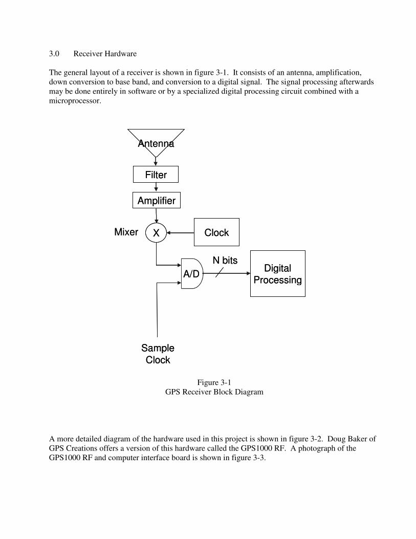
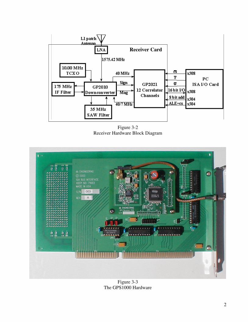
3.0 Receiver Hardware The general layout of a receiver is shown in figure 3-1. It consists of an antenna, amplification, down conversion to base band, and conversion to a digital signal. The signal processing afterwards may be done entirely in software or by a specialized digital processing circuit combined with a microprocessor. Figure 3-1 GPS Receiver Block Diagram A more detailed diagram of the hardware used in this project is shown in figure 3-2. Doug Baker of GPS Creations offers a version of this hardware called the GPS1000 RF. A photograph of the GPS1000 RF and computer interface board is shown in figure 3-3. Antenna Amplifier Filter Clock X A/D Sample Clock N bits Digital Processing Mixer Antenna Amplifier Filter Clock X A/D Sample Clock N bits Digital Processing Mixer
Transcript of Filter Amplifier Mixer Clock X lock N bits A/D Digital...
3.0 Receiver Hardware The general layout of a receiver is shown in figure 3-1. It consists of an antenna, amplification, down conversion to base band, and conversion to a digital signal. The signal processing afterwards may be done entirely in software or by a specialized digital processing circuit combined with a microprocessor.
Figure 3-1 GPS Receiver Block Diagram
A more detailed diagram of the hardware used in this project is shown in figure 3-2. Doug Baker of GPS Creations offers a version of this hardware called the GPS1000 RF. A photograph of the GPS1000 RF and computer interface board is shown in figure 3-3.
Antenna
Amplifier
Filter
ClockX
A/D
SampleClock
N bitsDigital
Processing
Mixer
Antenna
Amplifier
Filter
ClockX
A/D
SampleClock
N bitsDigital
Processing
Mixer
2
Figure 3-2 Receiver Hardware Block Diagram
Figure 3-3
The GPS1000 Hardware
Receiver Card
3
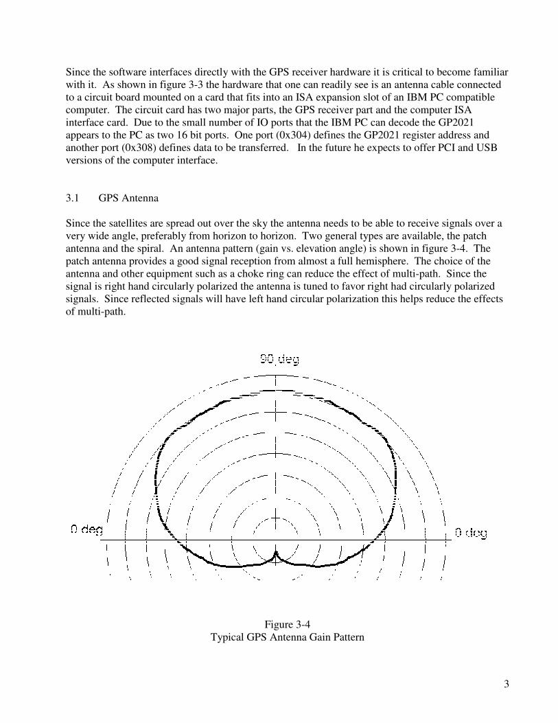
Since the software interfaces directly with the GPS receiver hardware it is critical to become familiar with it. As shown in figure 3-3 the hardware that one can readily see is an antenna cable connected to a circuit board mounted on a card that fits into an ISA expansion slot of an IBM PC compatible computer. The circuit card has two major parts, the GPS receiver part and the computer ISA interface card. Due to the small number of IO ports that the IBM PC can decode the GP2021 appears to the PC as two 16 bit ports. One port (0x304) defines the GP2021 register address and another port (0x308) defines data to be transferred. In the future he expects to offer PCI and USB versions of the computer interface. 3.1 GPS Antenna Since the satellites are spread out over the sky the antenna needs to be able to receive signals over a very wide angle, preferably from horizon to horizon. Two general types are available, the patch antenna and the spiral. An antenna pattern (gain vs. elevation angle) is shown in figure 3-4. The patch antenna provides a good signal reception from almost a full hemisphere. The choice of the antenna and other equipment such as a choke ring can reduce the effect of multi-path. Since the signal is right hand circularly polarized the antenna is tuned to favor right had circularly polarized signals. Since reflected signals will have left hand circular polarization this helps reduce the effects of multi-path.
Figure 3-4 Typical GPS Antenna Gain Pattern
4
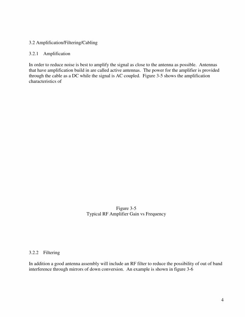
3.2 Amplification/Filtering/Cabling 3.2.1 Amplification In order to reduce noise is best to amplify the signal as close to the antenna as possible. Antennas that have amplification build in are called active antennas. The power for the amplifier is provided through the cable as a DC while the signal is AC coupled. Figure 3-5 shows the amplification characteristics of
Figure 3-5 Typical RF Amplifier Gain vs Frequency
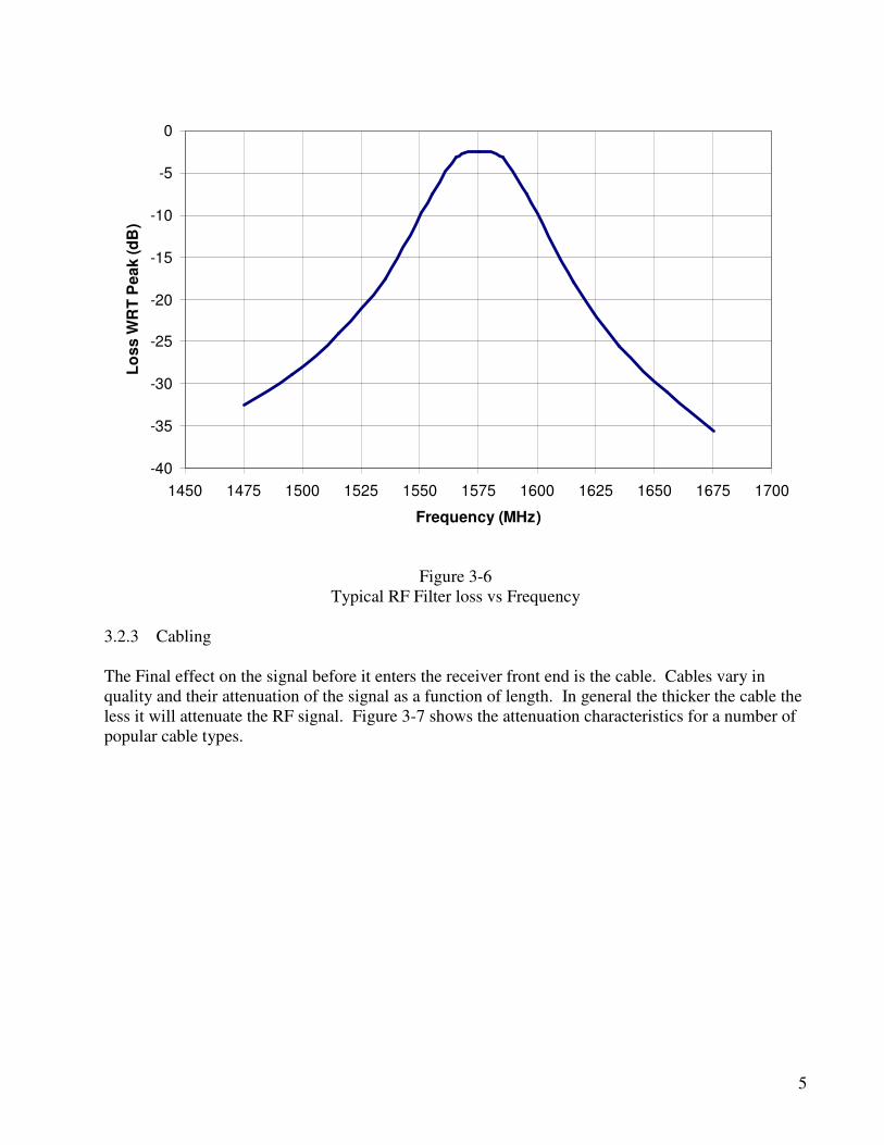
3.2.2 Filtering In addition a good antenna assembly will include an RF filter to reduce the possibility of out of band interference through mirrors of down conversion. An example is shown in figure 3-6
5
-40
-35
-30
-25
-20
-15
-10
-5
0
1450 1475 1500 1525 1550 1575 1600 1625 1650 1675 1700
Frequency (MHz)
Loss
WR
T P
eak
(dB
)
Figure 3-6 Typical RF Filter loss vs Frequency
3.2.3 Cabling The Final effect on the signal before it enters the receiver front end is the cable. Cables vary in quality and their attenuation of the signal as a function of length. In general the thicker the cable the less it will attenuate the RF signal. Figure 3-7 shows the attenuation characteristics for a number of popular cable types.

6
Figure 3-7 RF cable Loss vs Frequency
7
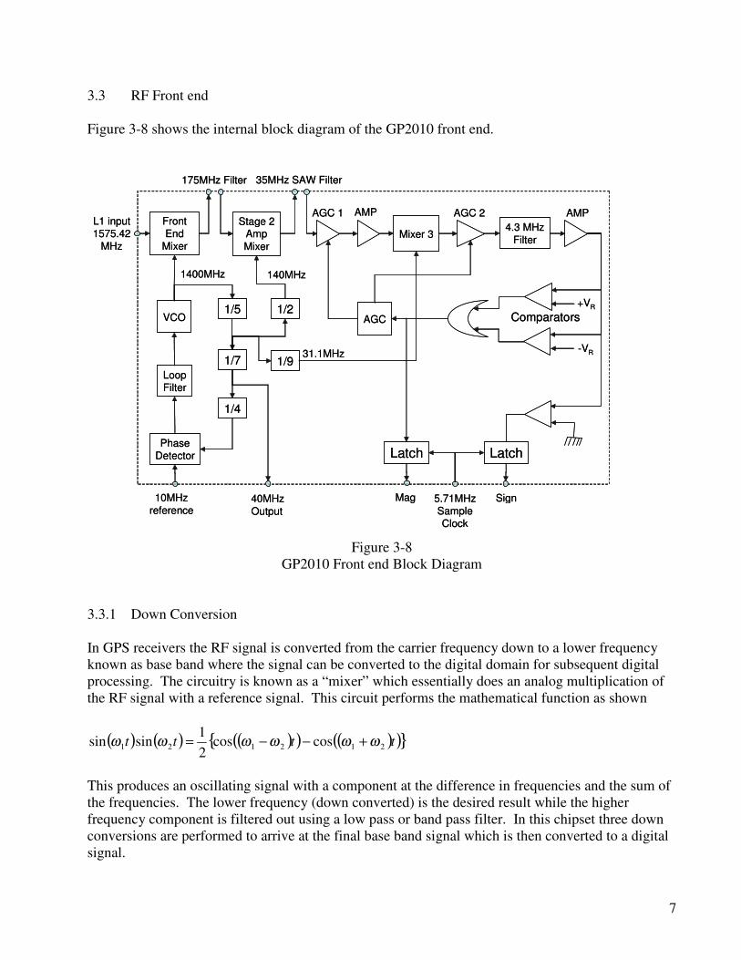
3.3 RF Front end Figure 3-8 shows the internal block diagram of the GP2010 front end.
Figure 3-8 GP2010 Front end Block Diagram
3.3.1 Down Conversion In GPS receivers the RF signal is converted from the carrier frequency down to a lower frequency known as base band where the signal can be converted to the digital domain for subsequent digital processing. The circuitry is known as a “mixer” which essentially does an analog multiplication of the RF signal with a reference signal. This circuit performs the mathematical function as shown
( ) ( ) ( )( ) ( )( ){ }tttt 212121 coscos21
sinsin ωωωωωω +−−=
This produces an oscillating signal with a component at the difference in frequencies and the sum of the frequencies. The lower frequency (down converted) is the desired result while the higher frequency component is filtered out using a low pass or band pass filter. In this chipset three down conversions are performed to arrive at the final base band signal which is then converted to a digital signal.
FrontEnd
Mixer
Stage 2AmpMixer
Mixer 3
AGC 1 AMP AGC 24.3 MHz
Filter
AMP
AGC
Latch LatchPhase
Detector
LoopFilter
VCO1/5
1/7
1/4
1/2
1/9
175MHz Filter 35MHz SAW Filter
40MHzOutput
5.71MHzSampleClock
Mag Sign
+VR
-VR
1400MHz 140MHz
31.1MHz
10MHzreference
L1 input1575.42
MHz
Comparators
FrontEnd
Mixer
Stage 2AmpMixer
Mixer 3
AGC 1 AMP AGC 24.3 MHz
Filter
AMP
AGC
Latch LatchPhase
Detector
LoopFilter
VCO1/5
1/7
1/4
1/2
1/9
175MHz Filter 35MHz SAW Filter
40MHzOutput
5.71MHzSampleClock
Mag Sign
+VR
-VR
1400MHz 140MHz
31.1MHz
10MHzreference
L1 input1575.42
MHz
Comparators
8
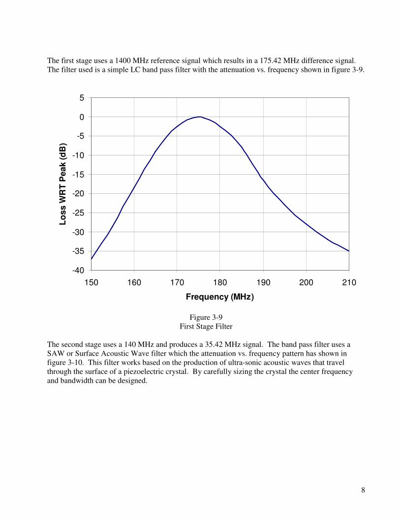
The first stage uses a 1400 MHz reference signal which results in a 175.42 MHz difference signal. The filter used is a simple LC band pass filter with the attenuation vs. frequency shown in figure 3-9.
-40
-35
-30
-25
-20
-15
-10
-5
0
5
150 160 170 180 190 200 210
Frequency (MHz)
Loss
WR
T P
eak
(dB
)
Figure 3-9
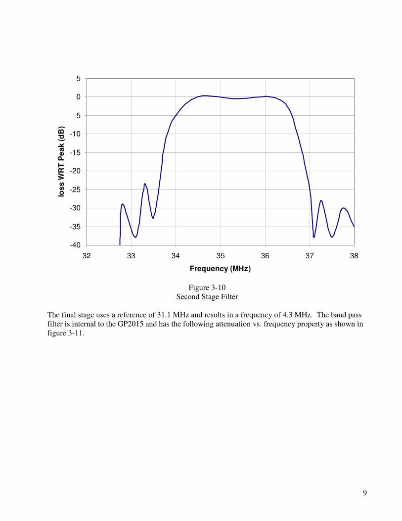
First Stage Filter The second stage uses a 140 MHz and produces a 35.42 MHz signal. The band pass filter uses a SAW or Surface Acoustic Wave filter which the attenuation vs. frequency pattern has shown in figure 3-10. This filter works based on the production of ultra-sonic acoustic waves that travel through the surface of a piezoelectric crystal. By carefully sizing the crystal the center frequency and bandwidth can be designed.
9
-40
-35
-30
-25
-20
-15
-10
-5
0
5
32 33 34 35 36 37 38
Frequency (MHz)
loss
WR
T P
eak
(dB
)
Figure 3-10
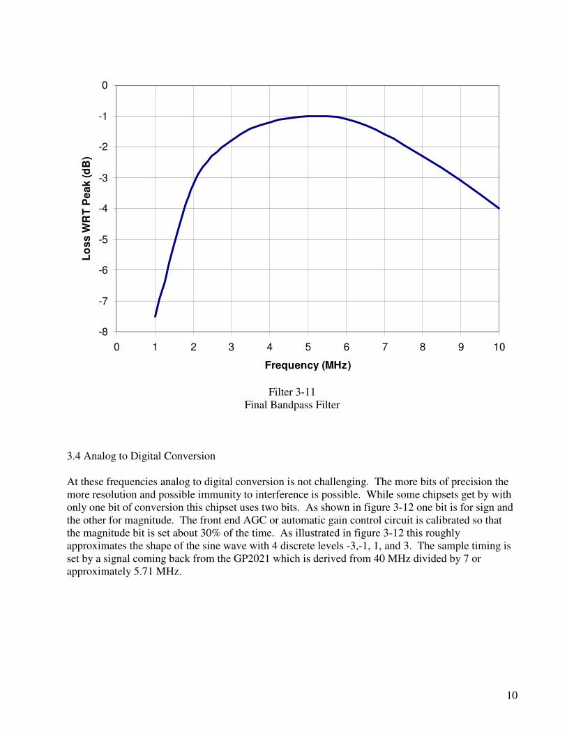
Second Stage Filter The final stage uses a reference of 31.1 MHz and results in a frequency of 4.3 MHz. The band pass filter is internal to the GP2015 and has the following attenuation vs. frequency property as shown in figure 3-11.
10
-8
-7
-6
-5
-4
-3
-2
-1
0
0 1 2 3 4 5 6 7 8 9 10
Frequency (MHz)
Loss
WR
T P
eak
(dB
)
Filter 3-11
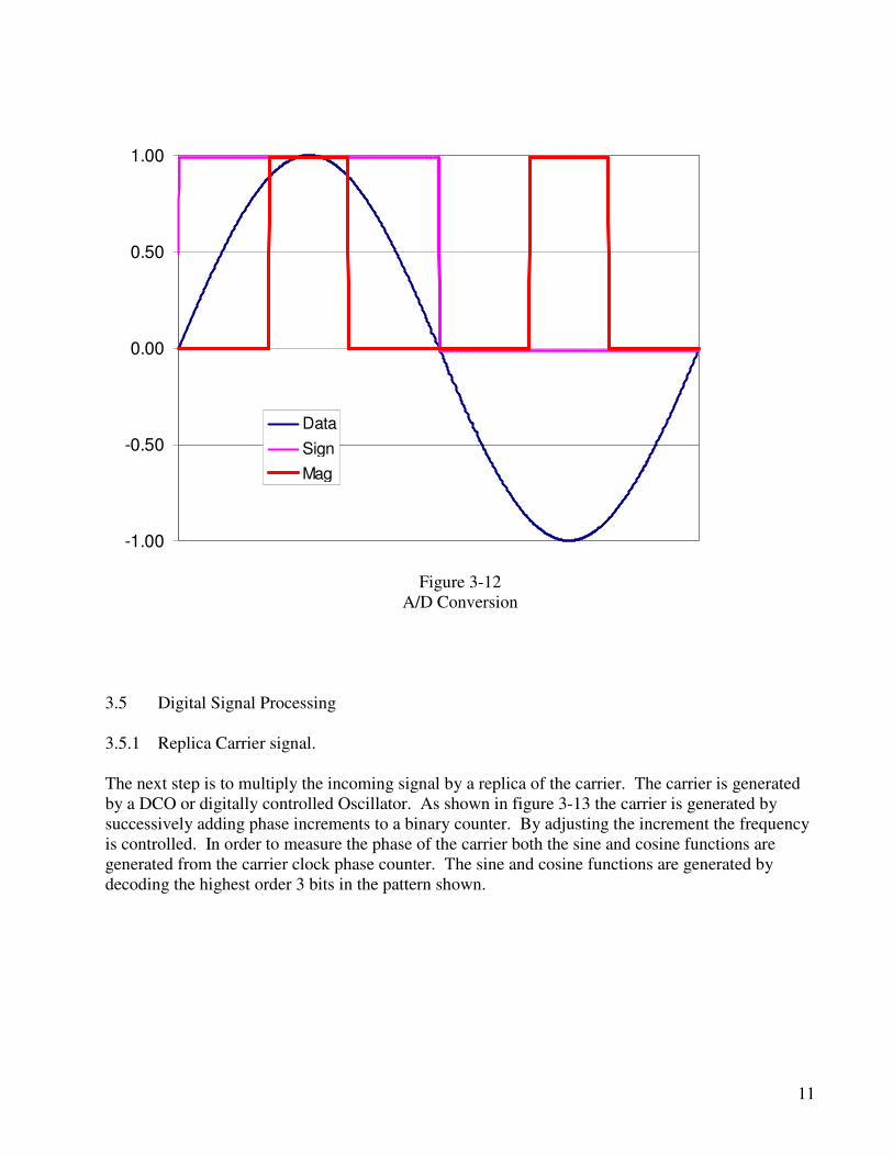
Final Bandpass Filter 3.4 Analog to Digital Conversion At these frequencies analog to digital conversion is not challenging. The more bits of precision the more resolution and possible immunity to interference is possible. While some chipsets get by with only one bit of conversion this chipset uses two bits. As shown in figure 3-12 one bit is for sign and the other for magnitude. The front end AGC or automatic gain control circuit is calibrated so that the magnitude bit is set about 30% of the time. As illustrated in figure 3-12 this roughly approximates the shape of the sine wave with 4 discrete levels -3,-1, 1, and 3. The sample timing is set by a signal coming back from the GP2021 which is derived from 40 MHz divided by 7 or approximately 5.71 MHz.
11
-1.00
-0.50
0.00
0.50
1.00
DataSignMag
Figure 3-12
A/D Conversion 3.5 Digital Signal Processing 3.5.1 Replica Carrier signal. The next step is to multiply the incoming signal by a replica of the carrier. The carrier is generated by a DCO or digitally controlled Oscillator. As shown in figure 3-13 the carrier is generated by successively adding phase increments to a binary counter. By adjusting the increment the frequency is controlled. In order to measure the phase of the carrier both the sine and cosine functions are generated from the carrier clock phase counter. The sine and cosine functions are generated by decoding the highest order 3 bits in the pattern shown.
12
Figure 3-13 Replica Carrier Generation
3.5.2 Replica code Another DCO is used to generate the frequency used to generate a replica of the PRN code for a particular satellite. The codes used in GPS are the type called “Gold” codes developed by Dr. Gold. Unlike the diagrams provided in ICD-GPS-200 the receiver hardware GP2021 uses a different more general method of generating the pseudo-random sequence (see figure 3-14). In order to bracket the peak of the correlation function two replicas are generated, one is ½ of a chip behind the other. To do this the clock for the code generator is run at twice the 1.023 MHz frequency that it is transmitted at.
Figure 3-14 Replica Code Generation
3.5.3 Correlation GPS digital signal processing chips such as the GP2021 have dedicated circuits to integrate the binary signal with carrier and code to produce correlation results. The correlation of the signal is accomplished by integrating over 1 ms and dumping the data to a register that can be read while the next integration is being performed.
13
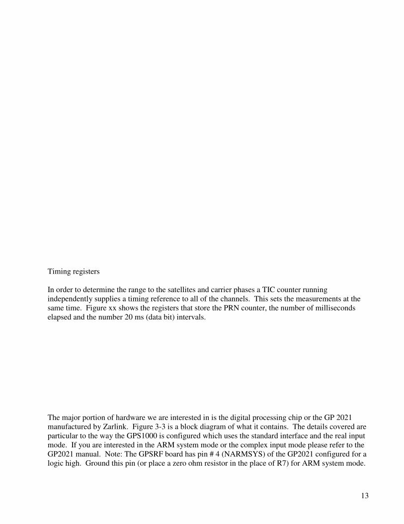
Timing registers In order to determine the range to the satellites and carrier phases a TIC counter running independently supplies a timing reference to all of the channels. This sets the measurements at the same time. Figure xx shows the registers that store the PRN counter, the number of milliseconds elapsed and the number 20 ms (data bit) intervals. The major portion of hardware we are interested in is the digital processing chip or the GP 2021 manufactured by Zarlink. Figure 3-3 is a block diagram of what it contains. The details covered are particular to the way the GPS1000 is configured which uses the standard interface and the real input mode. If you are interested in the ARM system mode or the complex input mode please refer to the GP2021 manual. Note: The GPSRF board has pin # 4 (NARMSYS) of the GP2021 configured for a logic high. Ground this pin (or place a zero ohm resistor in the place of R7) for ARM system mode.
14
Figure 3-15 GP2021 Block Diagram
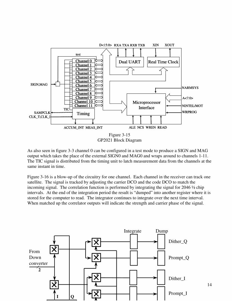
As also seen in figure 3-3 channel 0 can be configured in a test mode to produce a SIGN and MAG output which takes the place of the external SIGN0 and MAG0 and wraps around to channels 1-11. The TIC signal is distributed from the timing unit to latch measurement data from the channels at the same instant in time. Figure 3-16 is a blow-up of the circuitry for one channel. Each channel in the receiver can track one satellite. The signal is tracked by adjusting the carrier DCO and the code DCO to match the incoming signal. The correlation function is performed by integrating the signal for 2046 ½ chip intervals. At the end of the integration period the result is “dumped” into another register where it is stored for the computer to read. The integrator continues to integrate over the next time interval. When matched up the correlator outputs will indicate the strength and carrier phase of the signal.
I Q
FromDownconverter
2
**
Integrate Dump
**
**
**
****
Prompt_I
Prompt_Q
Dither_I
Dither_Q
MicroprocessorInterface
A<7:0>
Dual UART Real Time Clock
D<15:0>
SIGN,MAG
SAMPCLKCLK_T,CLK_I
RXA TXA RXB TXB XIN XOUT
ALE NCS WREN READACCUM_INT MEAS_INT
NARMSYS
NINTEL/MOT
WRPROG
Channel 0Channel 1Channel 2Channel 3Channel 4Channel 5Channel 6Channel 7Channel 8Channel 9
Channel 10Channel 11
TimingTIC
test
MicroprocessorInterface
A<7:0>
Dual UART Real Time Clock
D<15:0>
SIGN,MAG
SAMPCLKCLK_T,CLK_I
RXA TXA RXB TXB XIN XOUT
ALE NCS WREN READACCUM_INT MEAS_INT
NARMSYS
NINTEL/MOT
WRPROG
Channel 0Channel 1Channel 2Channel 3Channel 4Channel 5Channel 6Channel 7Channel 8Channel 9
Channel 10Channel 11
Channel 0Channel 1Channel 2Channel 3Channel 4Channel 5Channel 6Channel 7Channel 8Channel 9
Channel 10Channel 11
TimingTIC
test
15
Figure 3-16 Single Channel Digital Processing Block Diagram
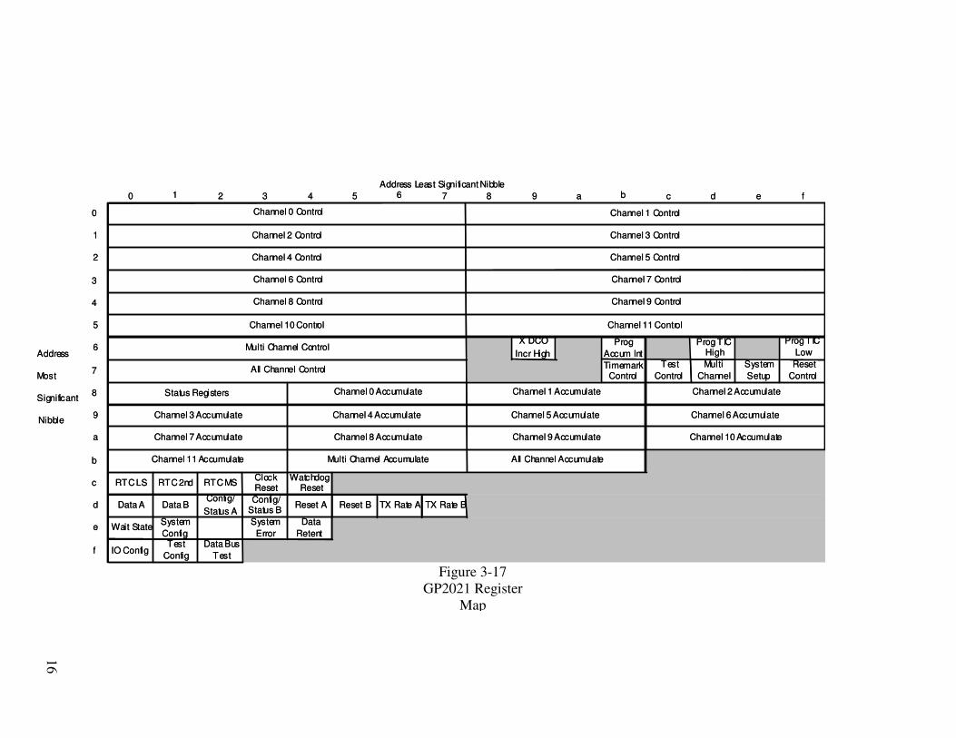
The GP2021 is structured as approximately 256 16 bit read/write registers which control all aspects of the signal processing. Table 2-I illustrates the functionality of the address space. Note that the read and write functions are generally different. The lower address space is a contiguous block devoted to channel control functions and reading measurements. Higher in the address space is a contiguous block devoted to reading correlation results. Miscellaneous other functions are spread throughout the address space. The measurement timing signal is called a “TIC” the default timing for the TIC is 100 ms although this can be changed by writing to the TIC register. When a TIC occurs the carrier phase and code phase registers are latched. These can be turned into pseudo-range and delta-pseudorange data.
16
Figure 3-17 GP2021 Register
Map
Address Least Significant Nibble0 1 2 3 4 5 6 7 8 9 a b c d e f
0
1
2
3
4
5
Address6
X DCO Incr High
Prog Accum Int
Prog TIC High
Prog TIC Low
Most 7 Timemark Control
Test Control
Multi Channel
System Setup
Reset Control
Significant 8
Nibble 9
a
b
c RTC LS RTC 2nd RTC MS Clock Reset
Watchdog Reset
d Data A Data BConfig/
Status AConfig/
Status B Reset A Reset B TX Rate A TX Rate B
e Wait State System Config
System Error
Data Retent
f IO ConfigTest
ConfigData Bus
Test
Channel 0 Control Channel 1 Control
Channel 2 Control
Channel 4 Control
Channel 6 Control
Channel 3 Control
Channel 5 Control
Channel 7 Control
Channel 9 Control
Channel 11 Control
Channel 8 Control
Channel 10 Control
Multi Channel Control
Status Registers Channel 0 Accumulate Channel 1 Accumulate Channel 2 Accumulate
Channel 3 Accumulate
Channel 7 Accumulate
Channel 4 Accumulate
Channel 8 Accumulate
Channel 5 Accumulate Channel 6 Accumulate
Channel 9 Accumulate Channel 10 Accumulate
Channel 11 Accumulate Multi Channel Accumulate All Channel Accumulate
All Channel Control
17
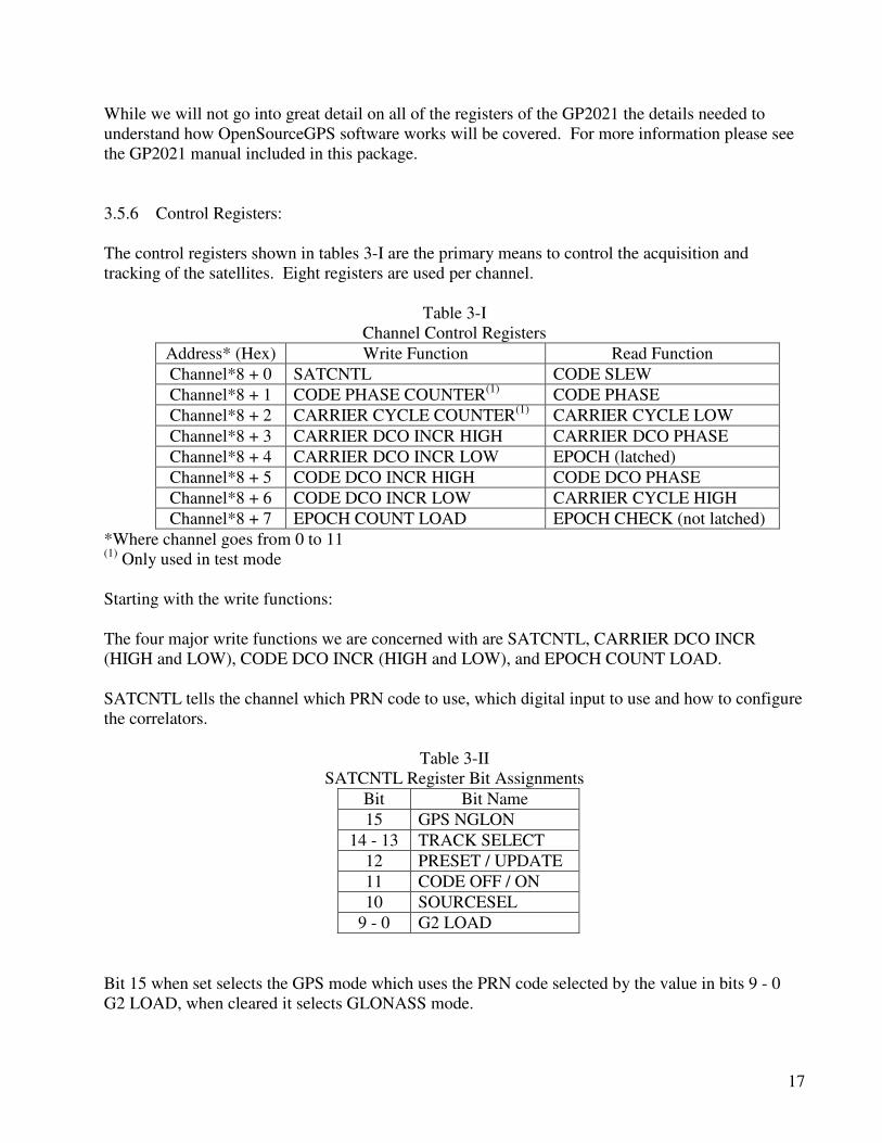
While we will not go into great detail on all of the registers of the GP2021 the details needed to understand how OpenSourceGPS software works will be covered. For more information please see the GP2021 manual included in this package. 3.5.6 Control Registers: The control registers shown in tables 3-I are the primary means to control the acquisition and tracking of the satellites. Eight registers are used per channel.
Table 3-I Channel Control Registers
Address* (Hex) Write Function Read Function Channel*8 + 0 SATCNTL CODE SLEW Channel*8 + 1 CODE PHASE COUNTER(1) CODE PHASE Channel*8 + 2 CARRIER CYCLE COUNTER(1) CARRIER CYCLE LOW Channel*8 + 3 CARRIER DCO INCR HIGH CARRIER DCO PHASE Channel*8 + 4 CARRIER DCO INCR LOW EPOCH (latched) Channel*8 + 5 CODE DCO INCR HIGH CODE DCO PHASE Channel*8 + 6 CODE DCO INCR LOW CARRIER CYCLE HIGH Channel*8 + 7 EPOCH COUNT LOAD EPOCH CHECK (not latched)
*Where channel goes from 0 to 11 (1) Only used in test mode Starting with the write functions: The four major write functions we are concerned with are SATCNTL, CARRIER DCO INCR (HIGH and LOW), CODE DCO INCR (HIGH and LOW), and EPOCH COUNT LOAD. SATCNTL tells the channel which PRN code to use, which digital input to use and how to configure the correlators.
Table 3-II SATCNTL Register Bit Assignments
Bit Bit Name 15 GPS NGLON
14 - 13 TRACK SELECT 12 PRESET / UPDATE 11 CODE OFF / ON 10 SOURCESEL
9 - 0 G2 LOAD Bit 15 when set selects the GPS mode which uses the PRN code selected by the value in bits 9 - 0 G2 LOAD, when cleared it selects GLONASS mode.
18
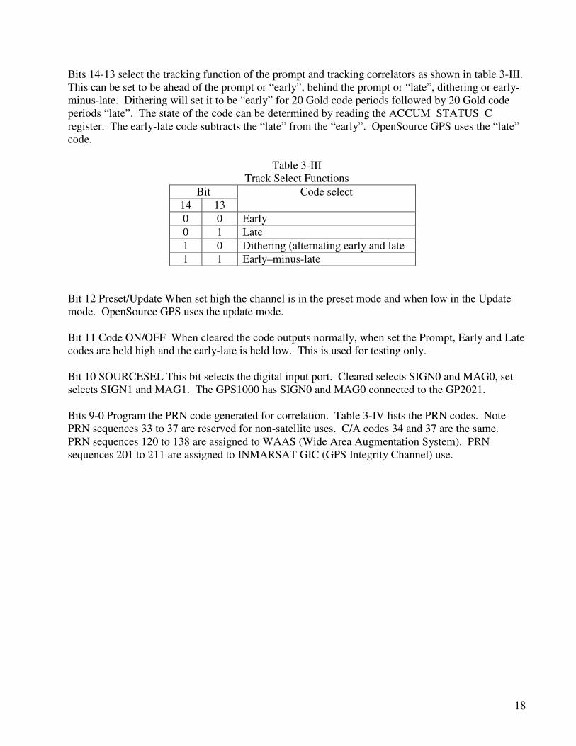
Bits 14-13 select the tracking function of the prompt and tracking correlators as shown in table 3-III. This can be set to be ahead of the prompt or “early”, behind the prompt or “late”, dithering or early-minus-late. Dithering will set it to be “early” for 20 Gold code periods followed by 20 Gold code periods “late”. The state of the code can be determined by reading the ACCUM_STATUS_C register. The early-late code subtracts the “late” from the “early”. OpenSource GPS uses the “late” code.
Table 3-III Track Select Functions
Bit 14 13
Code select
0 0 Early 0 1 Late 1 0 Dithering (alternating early and late 1 1 Early–minus-late
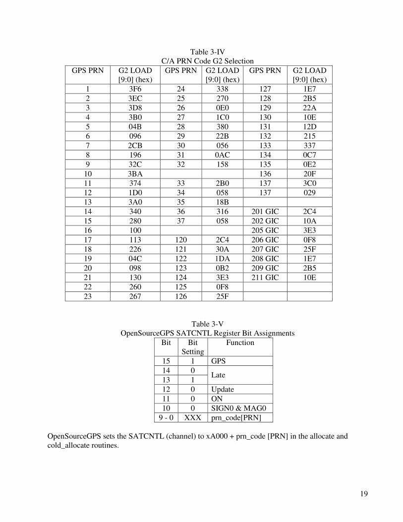
Bit 12 Preset/Update When set high the channel is in the preset mode and when low in the Update mode. OpenSource GPS uses the update mode. Bit 11 Code ON/OFF When cleared the code outputs normally, when set the Prompt, Early and Late codes are held high and the early-late is held low. This is used for testing only. Bit 10 SOURCESEL This bit selects the digital input port. Cleared selects SIGN0 and MAG0, set selects SIGN1 and MAG1. The GPS1000 has SIGN0 and MAG0 connected to the GP2021. Bits 9-0 Program the PRN code generated for correlation. Table 3-IV lists the PRN codes. Note PRN sequences 33 to 37 are reserved for non-satellite uses. C/A codes 34 and 37 are the same. PRN sequences 120 to 138 are assigned to WAAS (Wide Area Augmentation System). PRN sequences 201 to 211 are assigned to INMARSAT GIC (GPS Integrity Channel) use.
19
Table 3-IV C/A PRN Code G2 Selection
GPS PRN G2 LOAD [9:0] (hex)
GPS PRN G2 LOAD [9:0] (hex)
GPS PRN G2 LOAD [9:0] (hex)
1 3F6 24 338 127 1E7 2 3EC 25 270 128 2B5 3 3D8 26 0E0 129 22A 4 3B0 27 1C0 130 10E 5 04B 28 380 131 12D 6 096 29 22B 132 215 7 2CB 30 056 133 337 8 196 31 0AC 134 0C7 9 32C 32 158 135 0E2
10 3BA 136 20F 11 374 33 2B0 137 3C0 12 1D0 34 058 137 029 13 3A0 35 18B 14 340 36 316 201 GIC 2C4 15 280 37 058 202 GIC 10A 16 100 205 GIC 3E3 17 113 120 2C4 206 GIC 0F8 18 226 121 30A 207 GIC 25F 19 04C 122 1DA 208 GIC 1E7 20 098 123 0B2 209 GIC 2B5 21 130 124 3E3 211 GIC 10E 22 260 125 0F8 23 267 126 25F
Table 3-V OpenSourceGPS SATCNTL Register Bit Assignments
Bit Bit Setting
Function
15 1 GPS 14 0 13 1
Late
12 0 Update 11 0 ON 10 0 SIGN0 & MAG0
9 - 0 XXX prn_code[PRN] OpenSourceGPS sets the SATCNTL (channel) to xA000 + prn_code [PRN] in the allocate and cold_allocate routines.
20
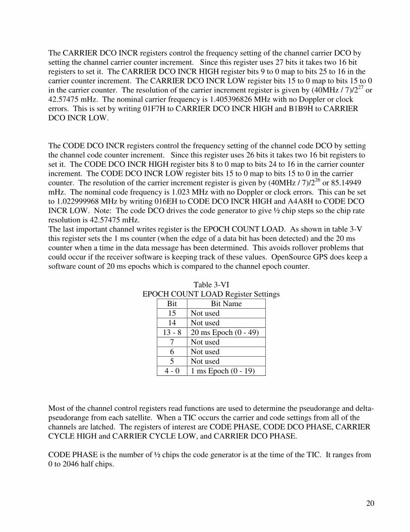
The CARRIER DCO INCR registers control the frequency setting of the channel carrier DCO by setting the channel carrier counter increment. Since this register uses 27 bits it takes two 16 bit registers to set it. The CARRIER DCO INCR HIGH register bits 9 to 0 map to bits 25 to 16 in the carrier counter increment. The CARRIER DCO INCR LOW register bits 15 to 0 map to bits 15 to 0 in the carrier counter. The resolution of the carrier increment register is given by (40MHz / 7)/227 or 42.57475 mHz. The nominal carrier frequency is 1.405396826 MHz with no Doppler or clock errors. This is set by writing 01F7H to CARRIER DCO INCR HIGH and B1B9H to CARRIER DCO INCR LOW. The CODE DCO INCR registers control the frequency setting of the channel code DCO by setting the channel code counter increment. Since this register uses 26 bits it takes two 16 bit registers to set it. The CODE DCO INCR HIGH register bits 8 to 0 map to bits 24 to 16 in the carrier counter increment. The CODE DCO INCR LOW register bits 15 to 0 map to bits 15 to 0 in the carrier counter. The resolution of the carrier increment register is given by (40MHz / 7)/226 or 85.14949 mHz. The nominal code frequency is 1.023 MHz with no Doppler or clock errors. This can be set to 1.022999968 MHz by writing 016EH to CODE DCO INCR HIGH and A4A8H to CODE DCO INCR LOW. Note: The code DCO drives the code generator to give ½ chip steps so the chip rate resolution is 42.57475 mHz. The last important channel writes register is the EPOCH COUNT LOAD. As shown in table 3-V this register sets the 1 ms counter (when the edge of a data bit has been detected) and the 20 ms counter when a time in the data message has been determined. This avoids rollover problems that could occur if the receiver software is keeping track of these values. OpenSource GPS does keep a software count of 20 ms epochs which is compared to the channel epoch counter.
Table 3-VI EPOCH COUNT LOAD Register Settings
Bit Bit Name 15 Not used 14 Not used
13 - 8 20 ms Epoch (0 - 49) 7 Not used 6 Not used 5 Not used
4 - 0 1 ms Epoch (0 - 19)
Most of the channel control registers read functions are used to determine the pseudorange and delta-pseudorange from each satellite. When a TIC occurs the carrier and code settings from all of the channels are latched. The registers of interest are CODE PHASE, CODE DCO PHASE, CARRIER CYCLE HIGH and CARRIER CYCLE LOW, and CARRIER DCO PHASE. CODE PHASE is the number of ½ chips the code generator is at the time of the TIC. It ranges from 0 to 2046 half chips.
21
CODE DCO PHASE is the 10 most significant bits of the code DCO accumulator. It ranges from 0 to 1023 and provides resolution down to 1/2048 of a chip or 15 cm. CARRIER CYCLE HIGH and LOW contain a 20 bit number of the positive going zero crossings of the carrier DCO since the last TIC. CARRIER DCO PHASE is an integer from 0 to 1023. It provides the carrier phase at the TIC in a resolution of 2π/1024 radians or 0.186 mm.
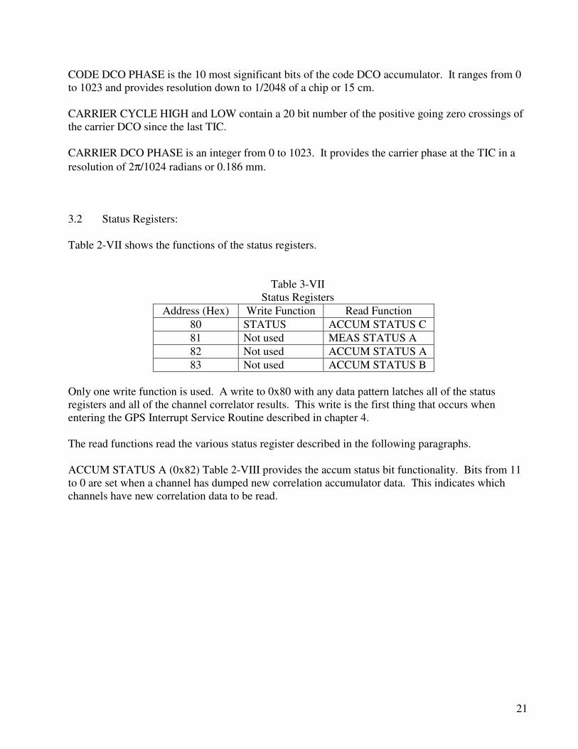
3.2 Status Registers: Table 2-VII shows the functions of the status registers.
Table 3-VII Status Registers
Address (Hex) Write Function Read Function 80 STATUS ACCUM STATUS C 81 Not used MEAS STATUS A 82 Not used ACCUM STATUS A 83 Not used ACCUM STATUS B
Only one write function is used. A write to 0x80 with any data pattern latches all of the status registers and all of the channel correlator results. This write is the first thing that occurs when entering the GPS Interrupt Service Routine described in chapter 4. The read functions read the various status register described in the following paragraphs. ACCUM STATUS A (0x82) Table 2-VIII provides the accum status bit functionality. Bits from 11 to 0 are set when a channel has dumped new correlation accumulator data. This indicates which channels have new correlation data to be read.
22
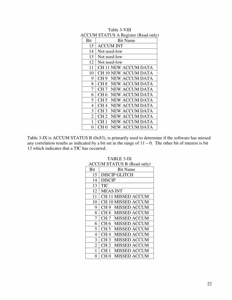
Table 3-VIII ACCUM STATUS A Register (Read only)
Bit Bit Name 15 ACCUM INT 14 Not used-low 13 Not used-low 12 Not used-low 11 CH 11 NEW ACCUM DATA 10 CH 10 NEW ACCUM DATA 9 CH 9 NEW ACCUM DATA 8 CH 8 NEW ACCUM DATA 7 CH 7 NEW ACCUM DATA 6 CH 6 NEW ACCUM DATA 5 CH 5 NEW ACCUM DATA 4 CH 4 NEW ACCUM DATA 3 CH 3 NEW ACCUM DATA 2 CH 2 NEW ACCUM DATA 1 CH 1 NEW ACCUM DATA 0 CH 0 NEW ACCUM DATA
Table 3-IX is ACCUM STATUS B (0x83), is primarily used to determine if the software has missed any correlation results as indicated by a bit set in the range of 11 – 0. The other bit of interest is bit 13 which indicates that a TIC has occurred.
TABLE 3-IX ACCUM STATUS B (Read only) Bit Bit Name
15 DISCIP GLITCH 14 DISCIP 13 TIC 12 MEAS INT 11 CH 11 MISSED ACCUM 10 CH 10 MISSED ACCUM 9 CH 9 MISSED ACCUM 8 CH 8 MISSED ACCUM 7 CH 7 MISSED ACCUM 6 CH 6 MISSED ACCUM 5 CH 5 MISSED ACCUM 4 CH 4 MISSED ACCUM 3 CH 3 MISSED ACCUM 2 CH 2 MISSED ACCUM 1 CH 1 MISSED ACCUM 0 CH 0 MISSED ACCUM
23
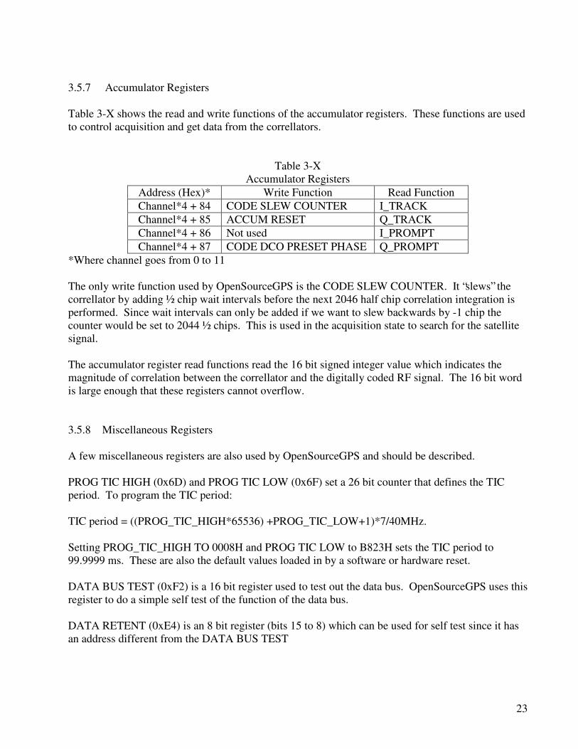
3.5.7 Accumulator Registers Table 3-X shows the read and write functions of the accumulator registers. These functions are used to control acquisition and get data from the correllators.
Table 3-X Accumulator Registers
Address (Hex)* Write Function Read Function Channel*4 + 84 CODE SLEW COUNTER I_TRACK Channel*4 + 85 ACCUM RESET Q_TRACK Channel*4 + 86 Not used I_PROMPT Channel*4 + 87 CODE DCO PRESET PHASE Q_PROMPT
*Where channel goes from 0 to 11 The only write function used by OpenSourceGPS is the CODE SLEW COUNTER. It “slews” the correllator by adding ½ chip wait intervals before the next 2046 half chip correlation integration is performed. Since wait intervals can only be added if we want to slew backwards by -1 chip the counter would be set to 2044 ½ chips. This is used in the acquisition state to search for the satellite signal. The accumulator register read functions read the 16 bit signed integer value which indicates the magnitude of correlation between the correllator and the digitally coded RF signal. The 16 bit word is large enough that these registers cannot overflow. 3.5.8 Miscellaneous Registers A few miscellaneous registers are also used by OpenSourceGPS and should be described. PROG TIC HIGH (0x6D) and PROG TIC LOW (0x6F) set a 26 bit counter that defines the TIC period. To program the TIC period: TIC period = ((PROG_TIC_HIGH*65536) +PROG_TIC_LOW+1)*7/40MHz. Setting PROG_TIC_HIGH TO 0008H and PROG TIC LOW to B823H sets the TIC period to 99.9999 ms. These are also the default values loaded in by a software or hardware reset. DATA BUS TEST (0xF2) is a 16 bit register used to test out the data bus. OpenSourceGPS uses this register to do a simple self test of the function of the data bus. DATA RETENT (0xE4) is an 8 bit register (bits 15 to 8) which can be used for self test since it has an address different from the DATA BUS TEST
24
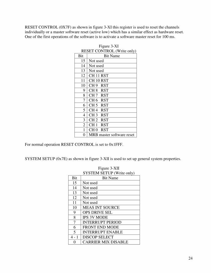
RESET CONTROL (0X7F) as shown in figure 3-XI this register is used to reset the channels individually or a master software reset (active low) which has a similar effect as hardware reset. One of the first operations of the software is to activate a software master reset for 100 ms.
Figure 3-XI RESET CONTROL (Write only)
Bit Bit Name 15 Not used 14 Not used 13 Not used 12 CH 11 RST 11 CH 10 RST 10 CH 9 RST 9 CH 8 RST 8 CH 7 RST 7 CH 6 RST 6 CH 5 RST 5 CH 4 RST 4 CH 3 RST 3 CH 2 RST 2 CH 1 RST 1 CH 0 RST 0 MRB master software reset
For normal operation RESET CONTROL is set to 0x1FFF. SYSTEM SETUP (0x7E) as shown in figure 3-XII is used to set up general system properties.
Figure 3-XII SYSTEM SETUP (Write only)
Bit Bit Name 15 Not used 14 Not used 13 Not used 12 Not used 11 Not used 10 MEAS INT SOURCE 9 OPS DRIVE SEL 8 IPS 3V MODE 7 INTERRUPT PERIOD 6 FRONT END MODE 5 INTERRUPT ENABLE
4 - 1 DISCOP SELECT 0 CARRIER MIX DISABLE
25
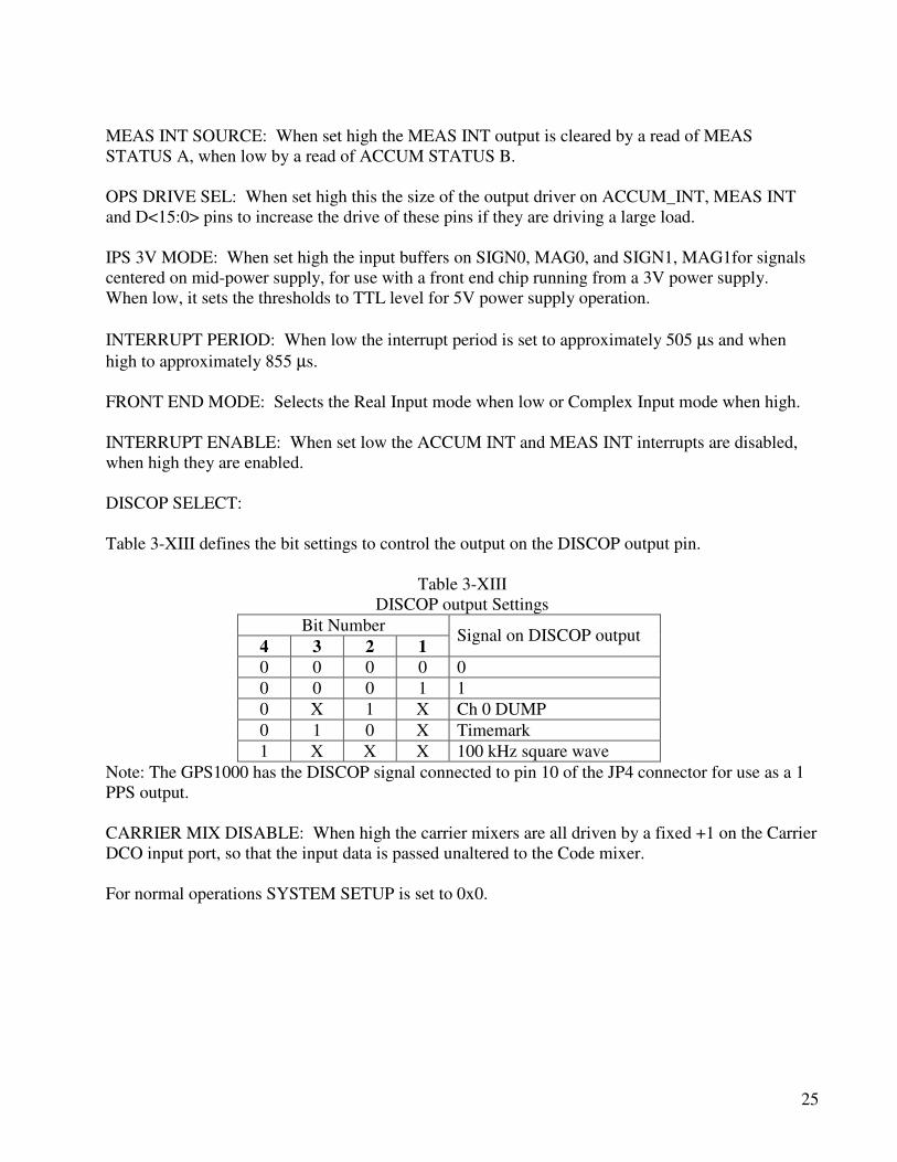
MEAS INT SOURCE: When set high the MEAS INT output is cleared by a read of MEAS STATUS A, when low by a read of ACCUM STATUS B. OPS DRIVE SEL: When set high this the size of the output driver on ACCUM_INT, MEAS INT and D<15:0> pins to increase the drive of these pins if they are driving a large load. IPS 3V MODE: When set high the input buffers on SIGN0, MAG0, and SIGN1, MAG1for signals centered on mid-power supply, for use with a front end chip running from a 3V power supply. When low, it sets the thresholds to TTL level for 5V power supply operation. INTERRUPT PERIOD: When low the interrupt period is set to approximately 505 µs and when high to approximately 855 µs. FRONT END MODE: Selects the Real Input mode when low or Complex Input mode when high. INTERRUPT ENABLE: When set low the ACCUM INT and MEAS INT interrupts are disabled, when high they are enabled. DISCOP SELECT: Table 3-XIII defines the bit settings to control the output on the DISCOP output pin.
Table 3-XIII DISCOP output Settings
Bit Number 4 3 2 1 Signal on DISCOP output
0 0 0 0 0 0 0 0 1 1 0 X 1 X Ch 0 DUMP 0 1 0 X Timemark 1 X X X 100 kHz square wave
Note: The GPS1000 has the DISCOP signal connected to pin 10 of the JP4 connector for use as a 1 PPS output. CARRIER MIX DISABLE: When high the carrier mixers are all driven by a fixed +1 on the Carrier DCO input port, so that the input data is passed unaltered to the Code mixer. For normal operations SYSTEM SETUP is set to 0x0.