
Files 3-Handouts Handout 6
27
EE- 203 Lectures on TTL and CMOS Dr Shei kh Sharif Iqbal, KFUPM
Transcript of Files 3-Handouts Handout 6
8/8/2019 Files 3-Handouts Handout 6
http://slidepdf.com/reader/full/files-3-handouts-handout-6 1/27
EE- 203
Lectures on TTL and CMOS
Dr Sheikh Sharif Iqbal, KFUPM

8/8/2019 Files 3-Handouts Handout 6
http://slidepdf.com/reader/full/files-3-handouts-handout-6 2/27
- In chapter 5, BJT operating in active mode is used to design Amplifier. Now we will concentrate on the other two modes. At one extreme BJT
operates in cutoff region (BJT OFF or IC≈ 0) and at other extreme
BJT operates in saturation region (BJT ON, maximum IC)
- If vi < 0.5 volt, the EBJ is reverse biased (R.B).
Since CBJ is also reverse biased (as V cc is ‘+’ )
BJT is OFF or operating in cutoff modeThus, I B=0 , I C =0 , I E =0 , V C =VCC
- If vi ≥ 0.7 volt, the EBJ is forward biased. If CBJ is still reverse biased
(if VC > 0.7) BJT is ON but in Active region (can’t be used as a switch)
- With ↑ vi ; IB ↑ resulting an ↑ VB and ↑ IC. Thus, VC will ↓ and when
VC < VB by 0.5v, CBJ will be F.B. As EBJ is still F.B BJT is Saturated
Thus, V BE = 0.7, V BC = 0.5, V CEsat = 0.2 , I Csat = (VCC - V CESat ) / RC and I B= I C / β Sat
5.3.4 & 5.10: Bipolar Junction Transistor (BJT) Switches: Reference: “Microelectronic Circuits by Sedra/Smith and EE-203 Online course, KFUPM
8/8/2019 Files 3-Handouts Handout 6
http://slidepdf.com/reader/full/files-3-handouts-handout-6 3/27
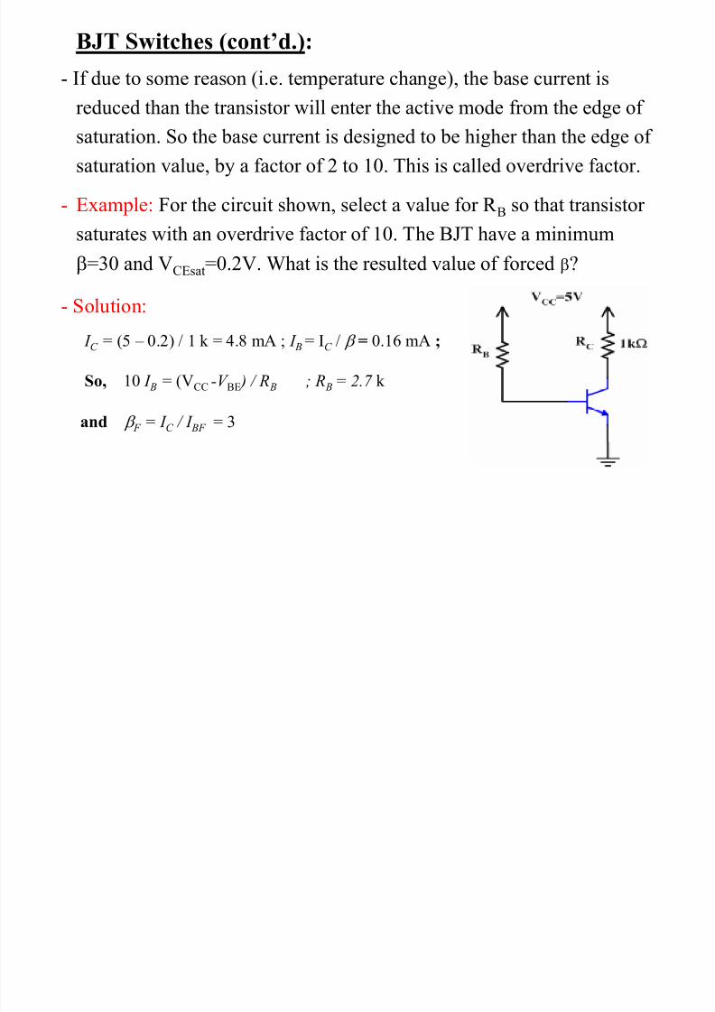
- Example: For the circuit shown, select a value for R B so that transistor
saturates with an overdrive factor of 10. The BJT have a minimum
β=30 and VCEsat=0.2V. What is the resulted value of forced β?
BJT Switches (cont’d.):
- If due to some reason (i.e. temperature change), the base current isreduced than the transistor will enter the active mode from the edge of
saturation. So the base current is designed to be higher than the edge of
saturation value, by a factor of 2 to 10. This is called overdrive factor.
I C
= (5 – 0.2) / 1 k = 4.8 mA ; I B
= IC
/ β = 0.16 mA ;
So, 10 I B = (VCC -V BE ) / R B ; R B = 2.7 k
and β F = I C / I BF = 3
- Solution:

8/8/2019 Files 3-Handouts Handout 6
http://slidepdf.com/reader/full/files-3-handouts-handout-6 4/27
BJT Switches Parameters:
- Internal capacitance of BJT introduces a time delay between the applicationof i B and the flow of iC . The measure of BJT's switching speed depends on
its delay-time ( t d ,n-sec), rise-time ( t r ,n-sec), turn-on-time ( t on), storage-time ( t s)
and turn-off-time ( t off
). Often larger ts constitute the limiting factor on S/W

8/8/2019 Files 3-Handouts Handout 6
http://slidepdf.com/reader/full/files-3-handouts-handout-6 5/27
- In this slide, logic level specification of digital circuits are presented.- Analog systems uses continuous property of electrical signals, whereas
in digital systems, electrical signals represent numbers. Typically in
binary digital circuits, it is customary to choose two predetermined DCvoltage levels to represent logic high ‘1’ or low ‘0’.
Chapter 10 10.1 Digital Logic Circuits:
- However, in order to allow for the inevitable
component tolerances and other effects that change
the signal voltage levels, two distinct voltage ranges
are usually used instead of two voltage values
- Thus, in digital circuits, if the signal voltage lies in
the range VL1 to VL2, the signal is interpreted as logic low or '0'. But if
signal voltage lies in the range VH1
to VH2
, the signal is interpreted as
logic high or '1'. Note, the undefined region voltages are never used.

8/8/2019 Files 3-Handouts Handout 6
http://slidepdf.com/reader/full/files-3-handouts-handout-6 6/27
Characteristics that are essential to successfully design digital circuits are;
(a) Allowable range of input and output voltage/current at gates
10.1: Characteristics of Digital Logic circuits:

8/8/2019 Files 3-Handouts Handout 6
http://slidepdf.com/reader/full/files-3-handouts-handout-6 7/27
(b) Noise Margin (≈ expressed in volt ): Noise margin is a measure of the
extent to which a logic circuit can tolerate noise or unwanted signals.
10.1: Characteristics of Digital Logic circuits: Cont’d…
ERROR

8/8/2019 Files 3-Handouts Handout 6
http://slidepdf.com/reader/full/files-3-handouts-handout-6 8/27
(c) - Fan-in of a logic gate is the number of its inputs driving the gate.
- Fan-out: The output of a logic gate often has to drive a number of other
gate inputs. However, a gate can only supply a limited amount of current.
Thus, fan-out of a gate is the maximum number of
10.1: Characteristics of Digital Logic circuits: ( Loading rule )
gates, allowed to be connected at the output of that gate, and are reliably driven by that gate.
- For logic high input, output of TTL inverter
will be logic low. Thus, it will sink current
from the load gates. Fan-out of this gate,
specifies the max. no. of load gates that are
successfully driven by the inverter output.
- If the inverter is sinking current from only one
gate, the internal voltage drop in ' I R1' is low
and vout =V R1= ' logic low' < V OL(max)
- But if the given inverter is driving 30 gates,'V R1' is high and vout > V OL(max) or ≠ 'logic 0‘ ERROR

8/8/2019 Files 3-Handouts Handout 6
http://slidepdf.com/reader/full/files-3-handouts-handout-6 9/27
(d) Propagation delay (≈ expressed in nano-seconds): t P is a measure of timetaken to change the output state after an input is applied. Thus,
t PHL time taken to change from ‘1’ to ‘0’ & t PLH time to change from ‘0’ to ‘1’
10.1: Characteristics of Digital Logic circuits: Cont’d….

8/8/2019 Files 3-Handouts Handout 6
http://slidepdf.com/reader/full/files-3-handouts-handout-6 10/27
(e) Power Dissipation (≈milliwatts): is the supplied power required to operate
the gate and is an important factor in designing portable digital products.
10.1: Characteristics of Digital Logic circuits: Cont’d….
(f) Delay power product ( should be as small as possible): is a figure of merit
that describe the gates power requirement and the related switching speed.

8/8/2019 Files 3-Handouts Handout 6
http://slidepdf.com/reader/full/files-3-handouts-handout-6 11/27
- Primary building block used in digital circuits are inverters:
- Simplest of logic inverter uses a voltage-controlled switch (figure below)
- In early days, the switch was made using only transistors and resistors,
constituents of the resistor transistor logic (RTL) family.
Evolution of Logic Gates DL gate RTL Inverters:
- If logic high input is applied to this transistor switch, the transistor
becomes saturated and the switch will be on. Consequently, the circuit
will sink current from any output device and the collector emitter saturation voltage (VCEsat), will appear in the output => logic low state
DL OR Gate RTL Inverter RTL Inverter

8/8/2019 Files 3-Handouts Handout 6
http://slidepdf.com/reader/full/files-3-handouts-handout-6 12/27
- If logic low input is applied to this transistor, the
transistor will cut off and the switch will be
open. Consequently, the circuit will source
current for any output device, and due to small
voltage drop in the collector resistor, the outputwill be at logic high. If no load is connected
with the output, as shown in the figure, Vcc will
appear in the output port => logic high or ‘1’
- The logic gates belonging to this family were very popular due to itsmicrochip- area-efficient design and the use of multi-emitter transistor.
- RTL switches were later improved by adding
diodes in the input stage called diode transistor
logic (DTL) circuits. Figure shows DTL NOR gate
- Further improvement of the DTL gates wereachieved by using multiple transistors, called
transistor transistor logic (TTL) circuits,
Improvement of Logic inverters; RTL DTL TTL :
DTL NOR
Gate
RTL
Inver -ter

8/8/2019 Files 3-Handouts Handout 6
http://slidepdf.com/reader/full/files-3-handouts-handout-6 13/27
- MOS is used to make voltage controlled switches,as it consumes low power and has very small size.
- In CMOS inverters, complementary switches
made of NMOS and PMOS are used as a pull-
down and pull-up networks, respectively.
- If Vin = logic low or ‘0’, the PMOS will be ON,
whereas the NMOS will remain OFF.
Consequently, the circuit will source current to
output device and Vout = logic high or ‘1’
- If Vin = logic high or ‘1’, the PMOS will be OFF,
whereas the NMOS will turn ON. Consequently,
the circuit will sink current from any output
device and circuit output, Vout = logic low or ‘0’
- BiCMOS combines advantages of TTL & CMOS
TTL CMOS Inverters BiCMOS : Active
Pull-up
Active
Pull-down
CMOS Inverter

8/8/2019 Files 3-Handouts Handout 6
http://slidepdf.com/reader/full/files-3-handouts-handout-6 14/27
Another Type (ECL) of Logic Inverters :
- Emitter coupled logic (ECL) gates uses double throw switches torealize logic inversion.
- This current steering logic arrangement is implemented using
differential amplifiers, & yields the fastest available digital logic gates.- This is because the ECL operates BJT’s in active modes, and thus don't
have storage time delay (from operating in Saturation and cutoff regions)
8/8/2019 Files 3-Handouts Handout 6
http://slidepdf.com/reader/full/files-3-handouts-handout-6 15/27
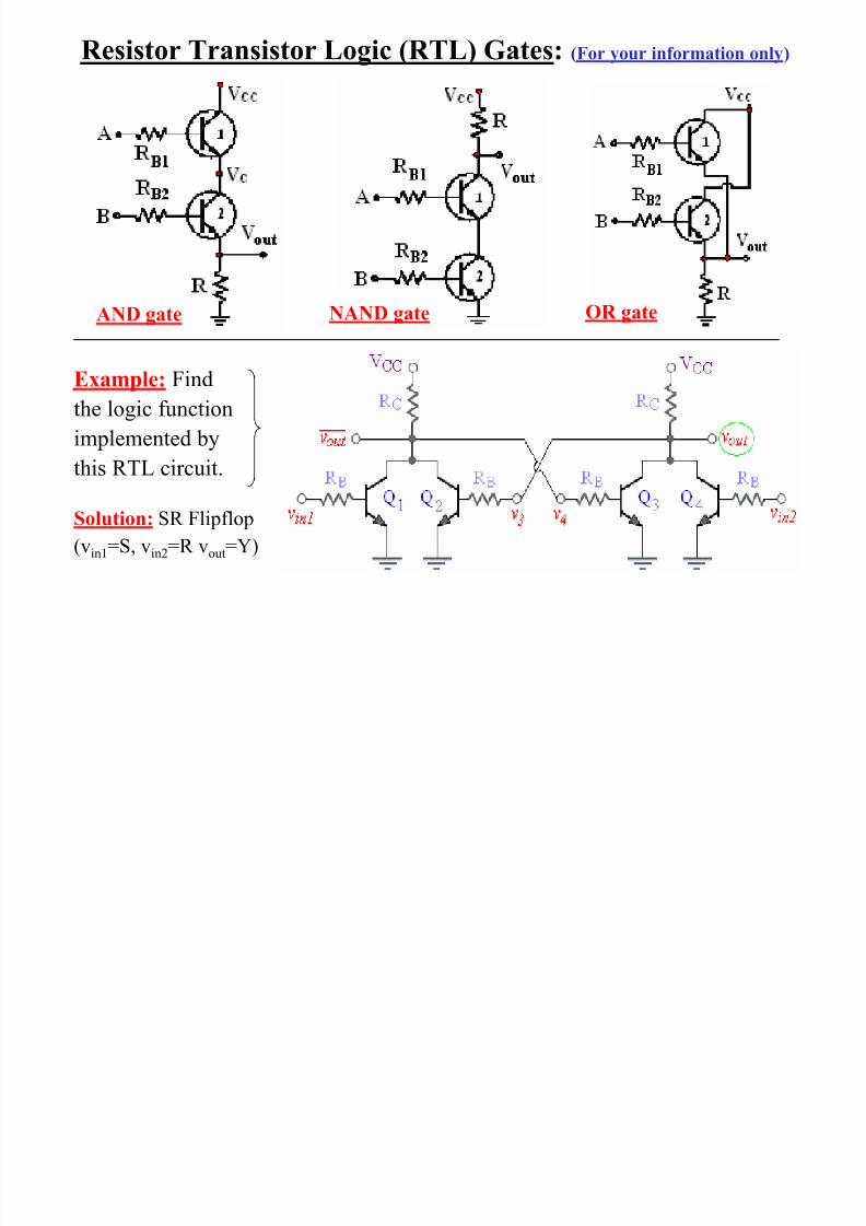
Resistor Transistor Logic (RTL) Gates: (For your information only)
AND gate NAND gateOR gate
Example: Find
the logic function
implemented by
this RTL circuit.
Solution: SR Flipflop
(vin1=S, vin2=R vout=Y)

8/8/2019 Files 3-Handouts Handout 6
http://slidepdf.com/reader/full/files-3-handouts-handout-6 16/27
- Evolved from DTL circuits. Diodes are replaced with multi-emeter BJT’s for
more area-efficient IC desing. In TTL, BJT’s operate in inverse active mode.- TTL has Input stage, Driver stage and Output stage.
Transistor-Transistor Logic (TTL) Inverter: (using BJT Switches)
Say VCC= 5 v , VD (any)= 0.7 v,
VCEsat(any)= 0.1v, VBE(any)= 0.7 v

8/8/2019 Files 3-Handouts Handout 6
http://slidepdf.com/reader/full/files-3-handouts-handout-6 17/27

8/8/2019 Files 3-Handouts Handout 6
http://slidepdf.com/reader/full/files-3-handouts-handout-6 18/27
TTL NAND Gates: As per design, Q1 inverse active (CBJ is FB & EBJ is RB)
Characteristics of TTL gates
8/8/2019 Files 3-Handouts Handout 6
http://slidepdf.com/reader/full/files-3-handouts-handout-6 19/27
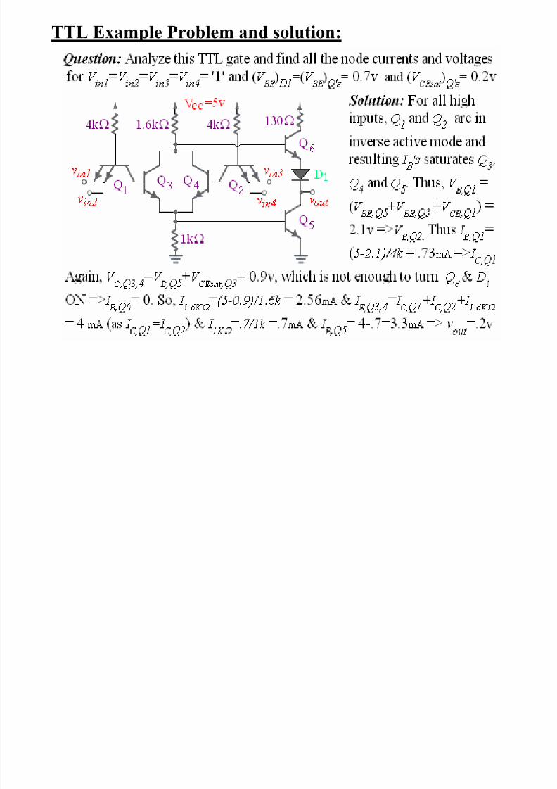
TTL Example Problem and solution:
8/8/2019 Files 3-Handouts Handout 6
http://slidepdf.com/reader/full/files-3-handouts-handout-6 20/27
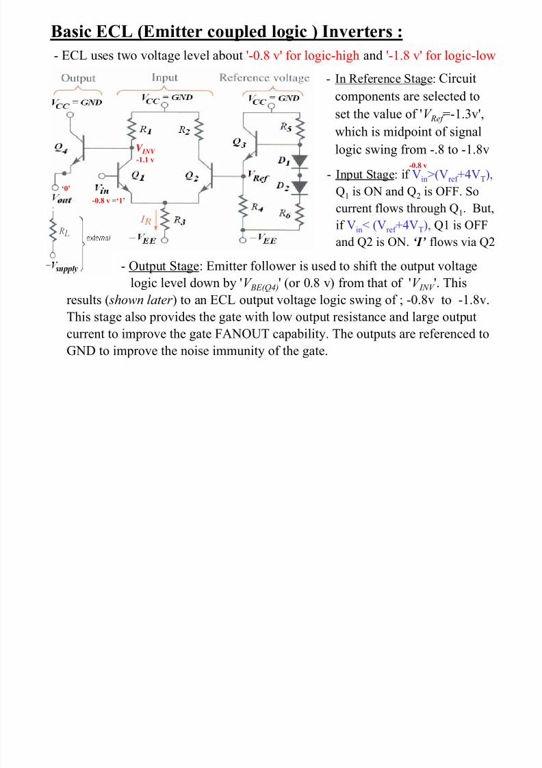
Basic ECL (Emitter coupled logic ) Inverters :
- ECL uses two voltage level about '-0.8 v' for logic-high and '-1.8 v' for logic-low
- In Reference Stage: Circuit
components are selected to
set the value of 'V Ref =-1.3v',
which is midpoint of signallogic swing from -.8 to -1.8v
- Output Stage: Emitter follower is used to shift the output voltagelogic level down by 'V BE(Q4)' (or 0.8 v) from that of 'V INV '. This
results ( shown later ) to an ECL output voltage logic swing of ; -0.8v to -1.8v.
This stage also provides the gate with low output resistance and large output
current to improve the gate FANOUT capability. The outputs are referenced toGND to improve the noise immunity of the gate.
V INV
- Input Stage: if Vin>(Vref +4VT),
Q1 is ON and Q2 is OFF. So
current flows through Q1. But,
if Vin< (Vref +4VT), Q1 is OFF
and Q2 is ON. ‘I’ flows via Q2
-0.8 v
-0.8 v =‘1’
-1.1 v
‘0’

8/8/2019 Files 3-Handouts Handout 6
http://slidepdf.com/reader/full/files-3-handouts-handout-6 21/27
10.2: CMOS Inverter: - MOS logic circuits dissipates much less power. The
high Zin of MOS allows temporary charge storage, applied in memory circuits. MOS
IC's has higher integration level due to optimized feature size and tight circuit packing.
For ‘0<vi<V t ’; since vGSN <V t Q N is OFF and since vSGP >V t Q
P
is ON. So Q P
pulls-up the
output to logic-high level.
Thus, v0 = V OH
For ‘Vt<vi<V IL’; SAT Q N acts
as a load and Q P remains ON.So Q P pulls-up the output to
logic-high level Thus, v0=V OH
For ‘VIL<vi<V IH ’; Q N and Q P
don’t act as switch. So this is a
forbidden region of operation
For ‘VIH<vi<V DD’; Q N is ON,
Q P acts as load or off . So theoutput is v0=V 0L
CMOS inverter
See 10.2 (pg 957) for equations for Noise Margin, R DSn , R DSp , Vth ..

8/8/2019 Files 3-Handouts Handout 6
http://slidepdf.com/reader/full/files-3-handouts-handout-6 22/27
Q’s are
either
Saturated
or
Cut-off
or
works asActive-
load
PDN
PUN
10.3.3: CMOS NAND Gate:
10.3.2: CMOS NOR Gate: Note pull-up network (PUN), Pull-down network (PDN)
PUN
PDN
PMOS
PUN and
NMOS
PDN

8/8/2019 Files 3-Handouts Handout 6
http://slidepdf.com/reader/full/files-3-handouts-handout-6 23/27
Example on CMOS:
10.3.4/5: Use Demorgan’s theorem (as in EE 200) to design the electronic circuit.
- Figure below: vout= vin3 + vin1 vin2 PUN and dual vout= vin3 . (vin1+ vin2) PDN
- For a complex logic function: Y = A(B+CD) A+B(C+D). And the followingCMOS circuit is shown in figure 10.14 of pg 968. Note the design of PUN & PDN’s

8/8/2019 Files 3-Handouts Handout 6
http://slidepdf.com/reader/full/files-3-handouts-handout-6 24/27
10.3.8: Transistor Sizing:
NMOS/PMOS, W/L selection is
Pg 973
For series connected MOSFET:
(W/L)Q’s
= 2n;
½ * 2n = n,or ≈ to that of a
basic inverter
For parallel connected MOSFET
(W/L)Q’s
= n/2
2*0.5n = n,or ≈ to that of a
basic inverter
8/8/2019 Files 3-Handouts Handout 6
http://slidepdf.com/reader/full/files-3-handouts-handout-6 25/27
BICOMOS logic gates:
BiCMOS is a VLSI technology that unites Bipolar and CMOS circuits on the
same chip to combine the advantages of both logic families. Consiquently,
BiCMOS digital gates enjoys both, the low-power, high- input-impedance and
wide-noise-margin of CMOS and the high current- driving-capability and
high-speed-switching of BJT
Furthermore, since BiCMOS technology is well suited for implementing high-
performance analog circuits, realization of both analog and digital functionson the same IC chip or 'system on a chip' becomes attainable.
BiCMOS Logic Gates are especially suitable for large capacitive loads
(greater than 0.5 pF or so) or when the logic gate has to drive a number of other logic gates, requiring large amount of output current.
Modern BiCMOS, invented by intel, was available in the market in 1992 and
was eventually used to construct VLSI chips for personal computers.

8/8/2019 Files 3-Handouts Handout 6
http://slidepdf.com/reader/full/files-3-handouts-handout-6 26/27
Basic BiCOMOS logic inverter:
• BiCMOS inverter consist of a CMOS inverter (Q P , Q N ) and a BJT output stage (Q1, Q2)
• For logic low input => Q N turns OFF, leading Q2 to remain OFF. But Q P turns ON
and supplies base current to Q1. Consequently, Q1 turns ON and supplies load current
• But, Q1 turns off when vout =V DD-V BE1 => Disadvantage: V OH <V DD by V BE1
• For logic high input => Q P turns OFF resulting Q1 to remain OFF. But Q N turns ON,
and the supplied base current turns Q2 ON, which provides a large current path to
quickly discharge capacitive load. Since, Q2 turns off when vout =V BE2, & leads to a
disadvantage of V OL= V BE2 ≠ '0’. Improvement bleeder-resistors, R 1 & R 2 R 1, not GNDed

8/8/2019 Files 3-Handouts Handout 6
http://slidepdf.com/reader/full/files-3-handouts-handout-6 27/27
Pass Transistor Logic (PTL) Circuits: Also called ‘transmission-gate logic'
• In PTL technology, logic circuits use series and/or parallel
combination of NMOS or CMOS switches to provide low
resistance paths to either VCC or GND. A PTL ‘AND gate’ is
shown in figure with logic function of; vout= vin1 .vin2 .vin3
• NMOS and CMOS switches for implementing PTL switches:
1 0
(a) operation during low-to-high transition of vin
(b) operation during high-to-low transition of vin
For CMOS switches, if vout = '0', vinC = VDD and vin changes state from low to high
(vin=> VDD) => transistors QN and QP both conducts. Thus, iout is the sum of; iDN=
0.5kn(VDD-Vtn-vo)2 and iDP= 0.5kp(VDD-|Vtn|)2. But as vo=>VDD-Vtn, iDN=>0,
although iDP continues to charge C until vo=VDD. Thus, tPHL of CMOS is lower then
NMOS due to extra initial current, iDP .For CMOS switch in fig. b, when vin=> 0, QN and QP interchanges roles.