
Figure 6.1. A 2-to-1 multiplexer. (a) Graphical symbol f s w 0 w 1 0 1 (b) Truth table 0 1 f f s w 0...
55
Figure 6.1. A 2-to-1 multiplexer. (a) Graphical symbol f s w 0 w 1 0 1 (b) Truth table 0 1 f f s w 0 w 1 (c) Sum-of-products circuit s w 0 w 1 (d) Circuit with transmission gates w 0 w 1 f s
-
Upload
collin-armstrong -
Category
Documents
-
view
231 -
download
2
Transcript of Figure 6.1. A 2-to-1 multiplexer. (a) Graphical symbol f s w 0 w 1 0 1 (b) Truth table 0 1 f f s w 0...
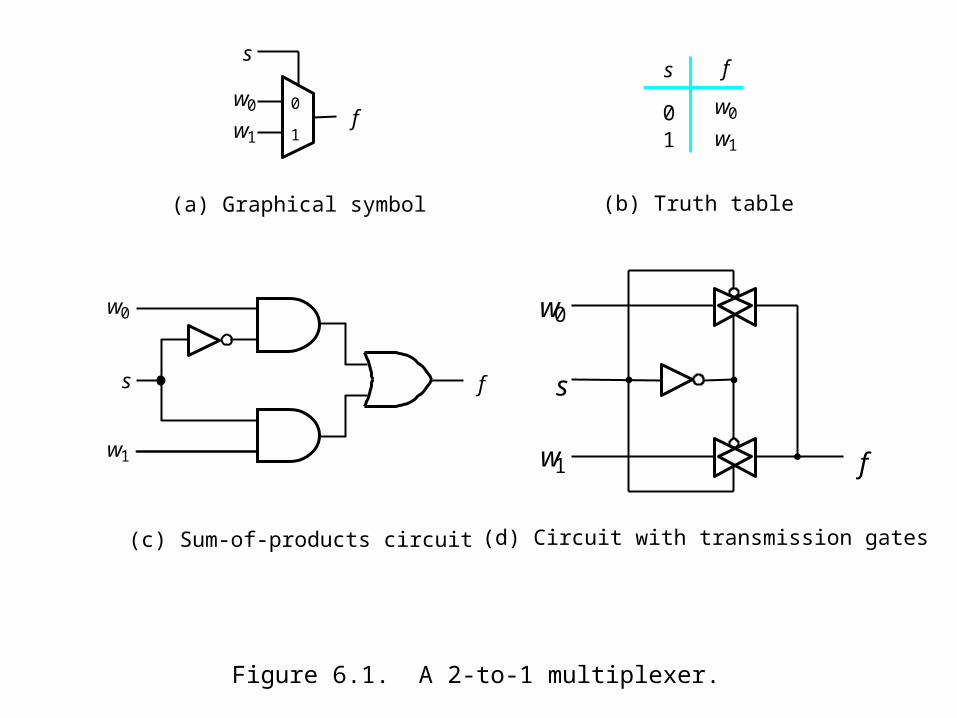
Figure 6.1. A 2-to-1 multiplexer.
(a) Graphical symbol
f
s
w0
w1
0
1
(b) Truth table
01
f
fs
w0
w1
(c) Sum-of-products circuit
s
w0
w1
(d) Circuit with transmission gates
w 0
w 1 f
s
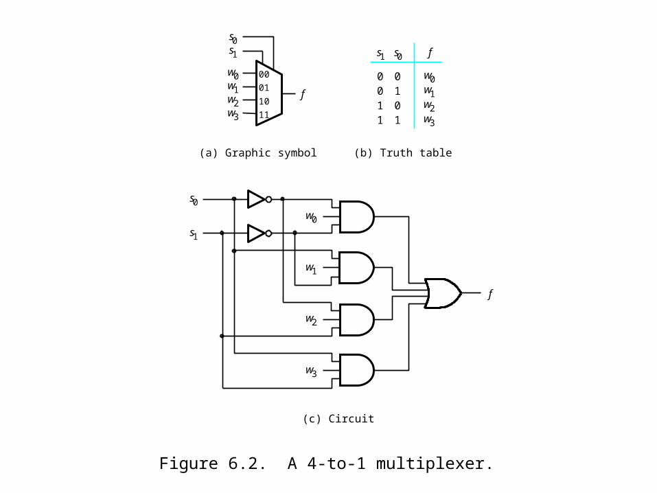
Figure 6.2. A 4-to-1 multiplexer.
f
s 1
w 0 w 1
00
01
(b) Truth table
w 0 w 1
s 0
w 2 w 3
10
11
0 0 1 1
1 0 1
f s 1
0
s 0
w 2 w 3
f
(c) Circuit
s 1
w 0
w 1
s 0
w 2
w 3
(a) Graphic symbol

Figure 6.3. Using 2-to-1 multiplexers to build a 4-to-1 multiplexer.
0
w 0
w 1
0
1
w 2
w 3
0
1
f 0
1
s 1
s
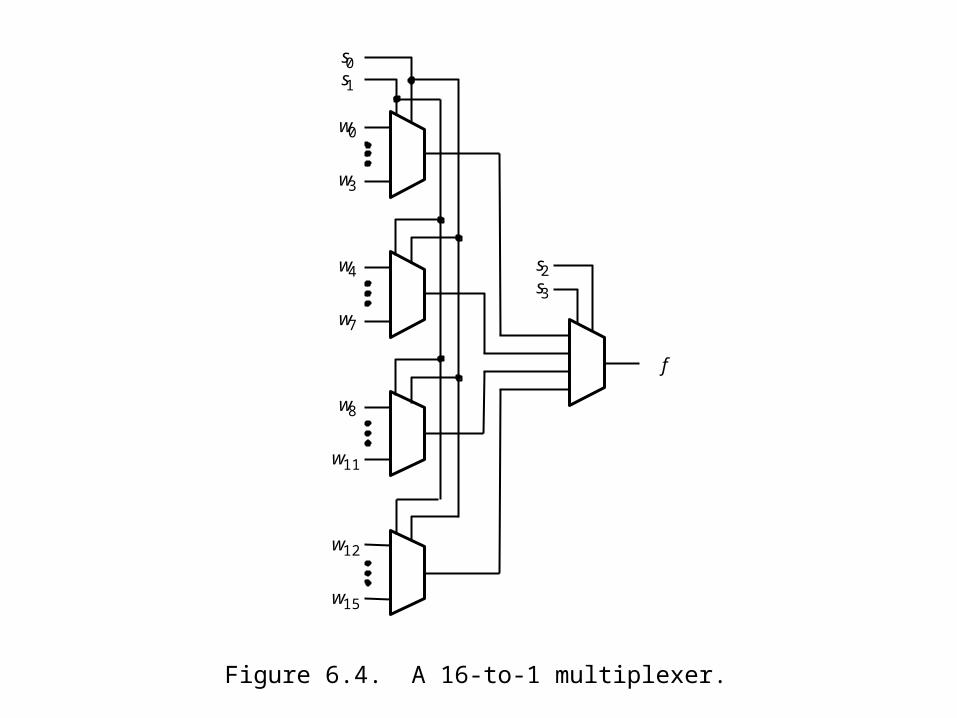
Figure 6.4. A 16-to-1 multiplexer.
w 8
w 11
s 1
w 0
s 0
w 3
w 4
w 7
w 12
w 15
s 3
s 2
f

Figure 6.5. A practical application of multiplexers.
x 1 0
1
x 2 0
1
s
y 1
y 2
x 1
x 2
y 1
y 2
(a) A 2x2 crossbar switch
(b) Implementation using multiplexers
s

Figure 6.6. Implementing programmable switches in an FPGA.
Please see “portrait orientation” PowerPoint file for Chapter 6

Figure 6.7. Synthesis of a logic function using multiplexers.
(a) Implementation using a 4-to-1 multiplexer
f
w 1
0 1
0
1
w 2
1 0
0
0
1
1
1
0
1
f w 1
0
w 2
1
0
(b) Modified truth table
0
1
0
0
1
1
1
0
1
f w 1
0
w 2
1
0
f w 2
w 1
0
1
f w 1
w 2
w 2
(c) Circuit

Figure 6.8. Three-input majority function.
w3
w3
f
w1
0
w2
1
(a) Modified truth table
(b) Circuit
00011
101
fw1
0
w2
1
0 00 11 01 1
0001
0 00 11 01 1
0111
w1 w2 w3 f
00001111
w3

Figure 6.9. Three-input XOR function implemented with 2-to-1 multiplexers.
(a) Truth table
0 00 11 01 1
0110
0 00 11 01 1
1001
w1 w2 w3 f
00001111
w2 w3
w2 w3
f
w3
w1
(b) Circuit
w2

Figure 6.10. Three-input XOR function implemented with a 4-to-1 multiplexer.
f
w 1
w 2
(a) Truth table (b) Circuit
0 0
0 1
1 0
1 1
0
1
1
0
0 0
0 1
1 0
1 1
1
0
0
1
w 1 w 2 w 3 f
0
0
0
0
1
1
1
1
w 3
w 3
w 3
w 3
w 3
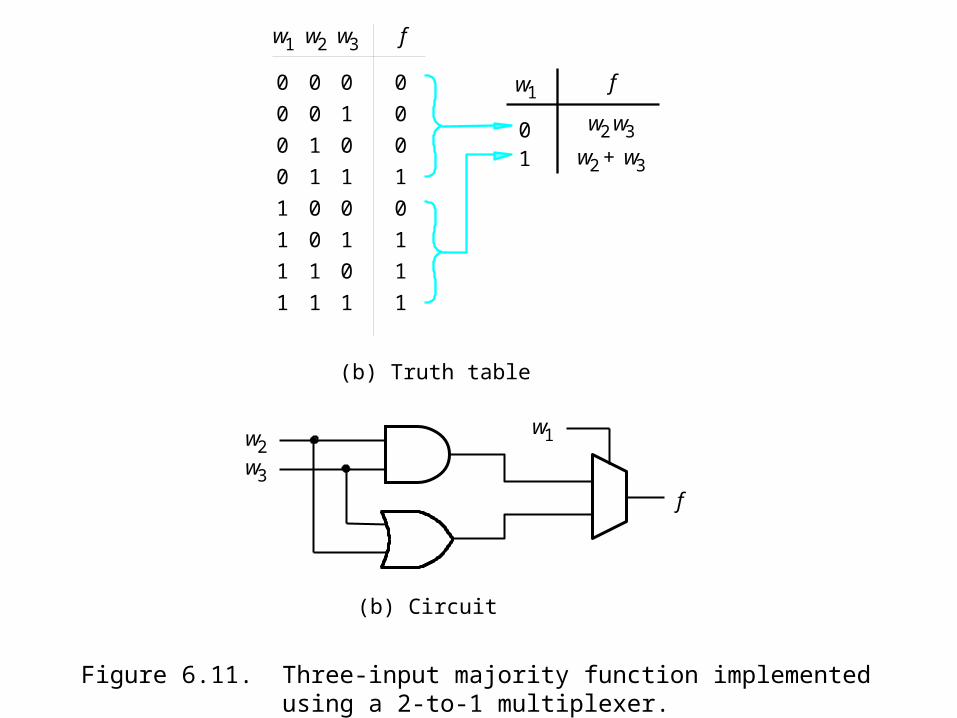
Figure 6.11. Three-input majority function implemented using a 2-to-1 multiplexer.
0 0
0 1
1 0
1 1
0
0
0
1
0 0
0 1
1 0
1 1
0
1
1
1
w 1 w 2 w 3 f
0
0
0
0
1
1
1
1
(b) Circuit
0 1
f w 1
w 2 w 3
w 2 w 3 +
f
w 3
w 1 w 2
(b) Truth table

Figure 6.12. Example circuits.
(a) Using a 2-to-1 multiplexer
f
w 2
w 1
w 3
f
w 1
w 2
w 3
(b) Using a 4-to-1 multiplexer
1

Figure 6.13. Example circuit.
w 2
0 w 3
1
f
w 1

Figure 6.14. Example circuits.
w 2 w 3
f
w 4
w 1
f w 1
(a) Using three 3-LUTs
(b) Using two 3-LUTs
f w 1
w 1 w 3
f
w 4
0 f w 2
w 2
0

Figure 6.15. An n-to-2n binary decoder.
0
w n 1 –
n inputs
EnEnable
2 n
outputs
y 0
y 2 n 1 –
w
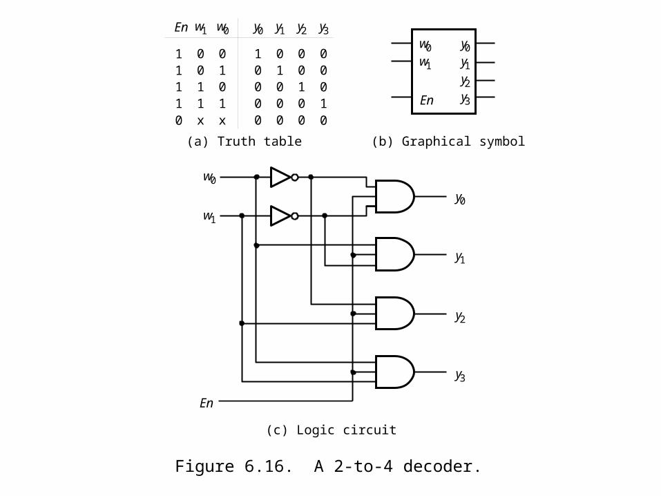
Figure 6.16. A 2-to-4 decoder.
0 0 1 1
1 0 1
y 0 w 1
0
w 0
(c) Logic circuit
w 1
w 0
x x
1 1
0
1 1
En
0 0 0
1
0
y 1
1 0 0
0
0
y 2
0 1 0
0
0
y 3
0 0 1
0
0
y 0
y 1
y 2
y 3
En
w 0
En
y 0 w 1 y 1
y 2 y 3
(a) Truth table (b) Graphical symbol
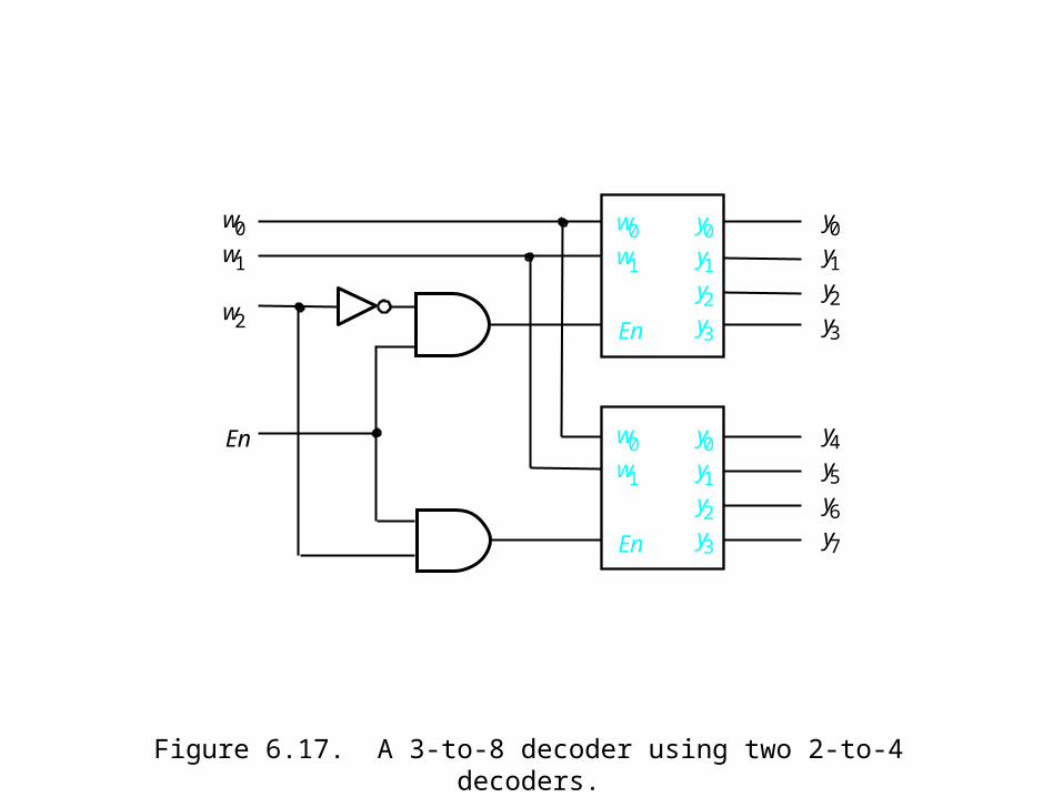
Figure 6.17. A 3-to-8 decoder using two 2-to-4 decoders.
w 2
w 0 y 0 y 1 y 2 y 3
w 0
En
y 0 w 1 y 1
y 2 y 3
w 0
En
y 0 w 1 y 1
y 2 y 3
y 4 y 5 y 6 y 7
w 1
En
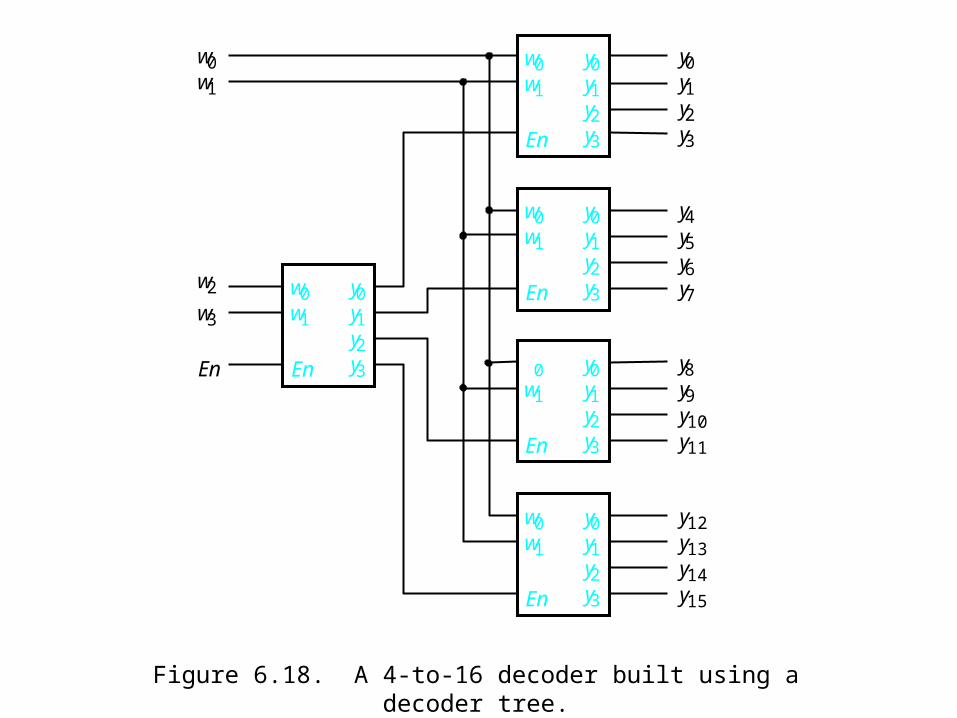
Figure 6.18. A 4-to-16 decoder built using a decoder tree.
w 0
En
y 0 w 1 y 1
y 2 y 3
y 8 y 9 y 10y 11
w 2
w 0 y 0 y 1 y 2 y 3
w 0
En
y 0 w 1 y 1
y 2 y 3
w 0
En
y 0 w 1 y 1
y 2 y 3
y 4 y 5 y 6 y 7
w 1
w 0
En
y 0 w 1 y 1
y 2 y 3
y 12y 13y 14y 15
w 0
En
y 0 w 1 y 1
y 2 y 3
w 3
En
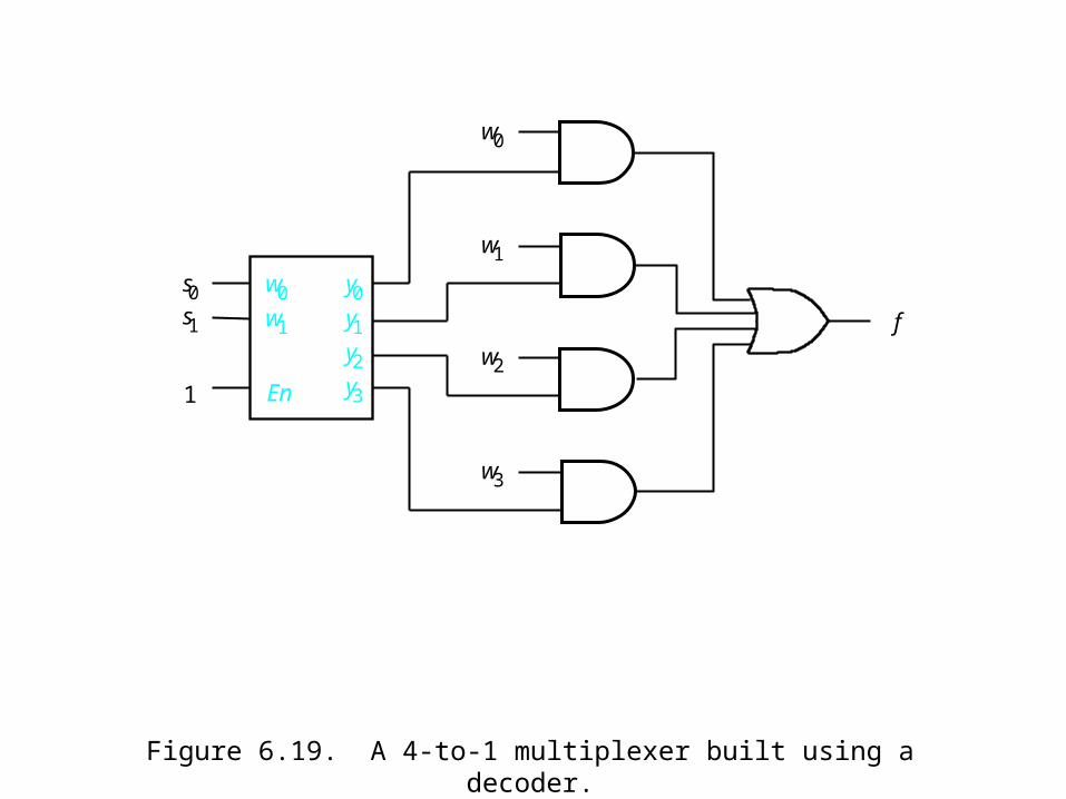
Figure 6.19. A 4-to-1 multiplexer built using a decoder.
w 1
w 0
w 0
En
y 0 w 1 y 1
y 2 y 3
w 2
w 3
f
s 0 s 1
1
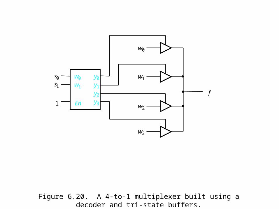
Figure 6.20. A 4-to-1 multiplexer built using a decoder and tri-state buffers.
w1
w0
w0
En
y0
w1 y1
y2
y3
f
s0s1
1 w2
w3

Figure 6.21. A 2m x n read-only memory (ROM) block.
Sel 2
Sel 1
Sel 0
Sel 2 m 1 –
Address
Read
d 0 d n 1 – d n 2 –
m -to-2
m deco
der
0/1 0/1 0/1
0/1 0/1 0/1
0/1 0/1 0/1
0/1 0/1 0/1
Data
a 0
a 1
a m 1 –
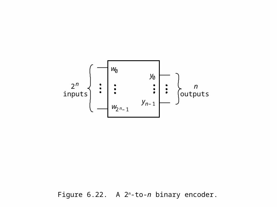
Figure 6.22. A 2n-to-n binary encoder.
2 n
inputs
w 0
w 2 n 1 –
y 0
y n 1 –
n outputs
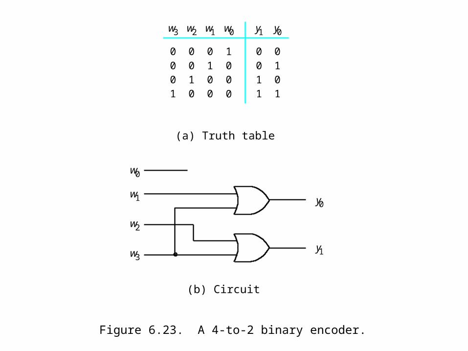
Figure 6.23. A 4-to-2 binary encoder.
0 0 1 1
1 0 1
w 3 y 1
0
y 0
(b) Circuit
w 1
w 0
0 0 1
0
w 2
0 1 0
0
w 1
1 0 0
0
w 0
0 0 0
1
y 0
w 2
w 3 y 1
(a) Truth table
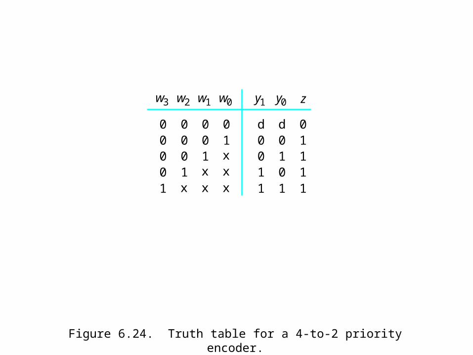
Figure 6.24. Truth table for a 4-to-2 priority encoder.
d001
010
w0 y1
d
y0
1 1
01
1
11
z
1xx
0
x
w1
01x
0
x
w2
001
0
x
w3
000
0
1
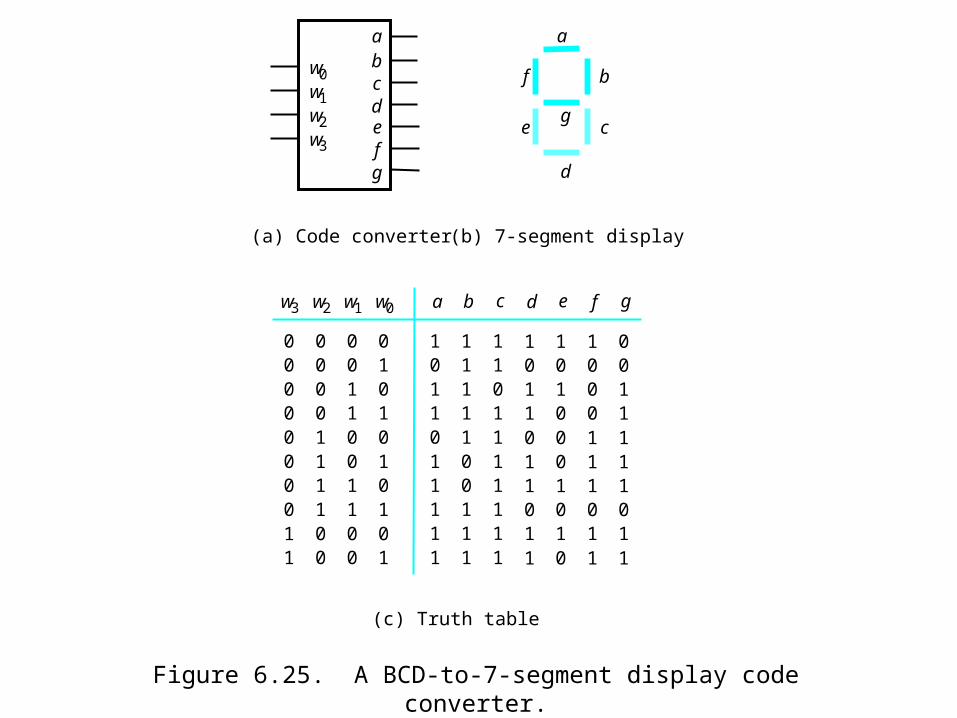
Figure 6.25. A BCD-to-7-segment display code converter.
c e
1 0 1 1
1 1 1
w 0 a
1
b
0 1
1 1
1
0 1
1 0 1
0
0
w 1
0 1 1
0
0
w 2
0 0 0
0
1
w 3
0 0 0
0
0
c
1 0 1 0
0 1 1 0
1 1 1 0
0 0 0 1
1 0 0 1
1 1 1 1
0 1 1
0
1 1
1 1
1
1 1
0 1 1
1
d
0
1 0
0
1 0
e
1 0 1
1
1
0 1
0
0 1
0 0 0
1
f
1
0 0
1
1 1
g
1 0 1
1
1
1 1
1
0 1
(c) Truth table
(a) Code converter
w 0
a
w 1
b c d w 2
w 3 e f g
a
g
b f
d
(b) 7-segment display
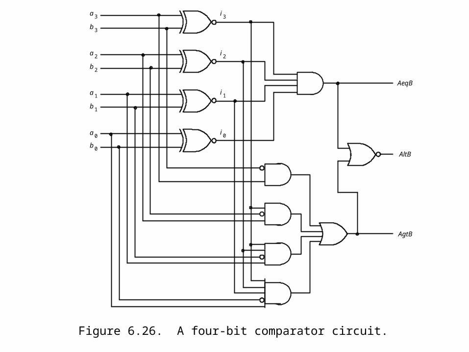
Figure 6.26. A four-bit comparator circuit.
i 0
i 1
i 2
i 3
b 0
a 0
b 1
a 1
b 2
a 2
b 3
a 3
AeqB
AgtB
AltB
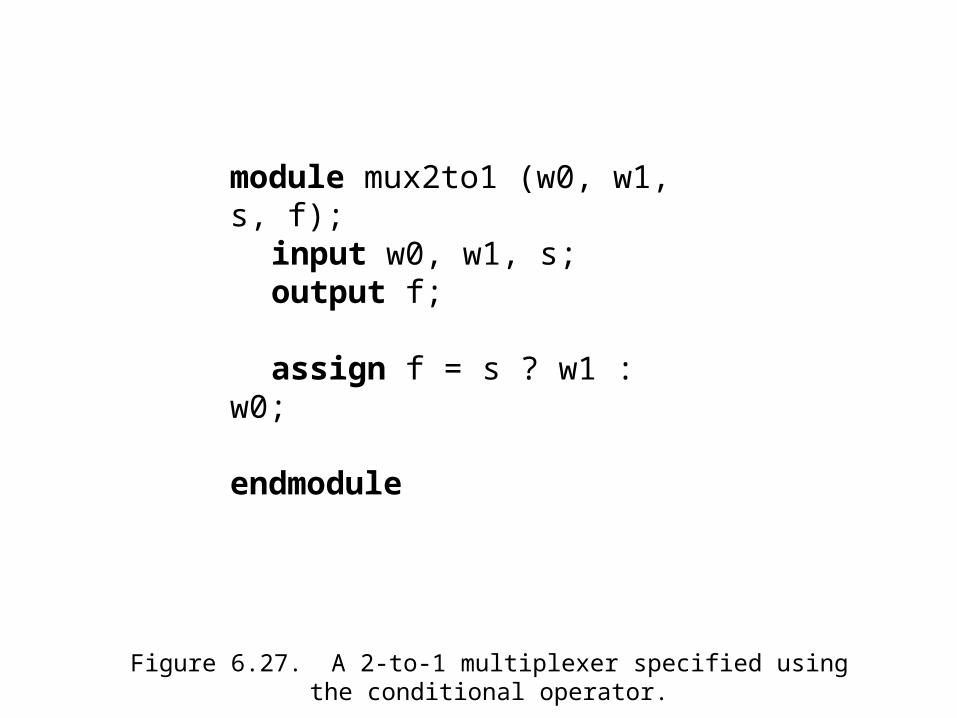
Figure 6.27. A 2-to-1 multiplexer specified using the conditional operator.
module mux2to1 (w0, w1, s, f);input w0, w1, s;output f;
assign f = s ? w1 : w0;
endmodule
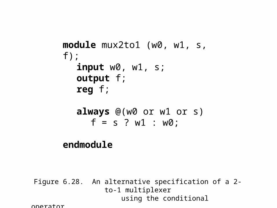
Figure 6.28. An alternative specification of a 2-to-1 multiplexer using the conditional operator.
module mux2to1 (w0, w1, s, f);input w0, w1, s;output f;reg f;
always @(w0 or w1 or s)f = s ? w1 : w0;
endmodule
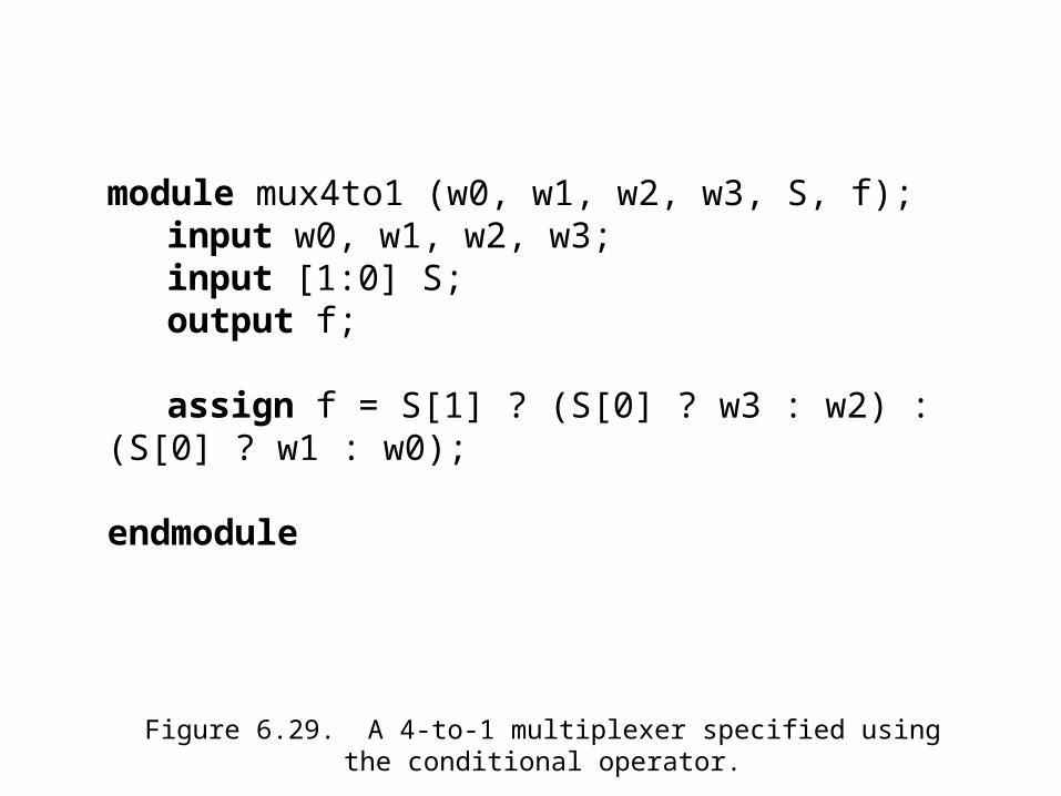
Figure 6.29. A 4-to-1 multiplexer specified using the conditional operator.
module mux4to1 (w0, w1, w2, w3, S, f);input w0, w1, w2, w3;input [1:0] S;output f;
assign f = S[1] ? (S[0] ? w3 : w2) : (S[0] ? w1 : w0);
endmodule
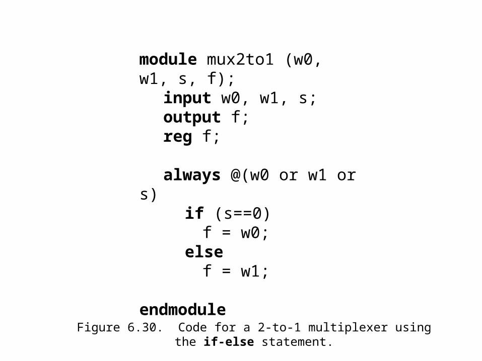
Figure 6.30. Code for a 2-to-1 multiplexer using the if-else statement.
module mux2to1 (w0, w1, s, f);input w0, w1, s;output f;reg f;
always @(w0 or w1 or s)if (s==0)
f = w0;else
f = w1;
endmodule
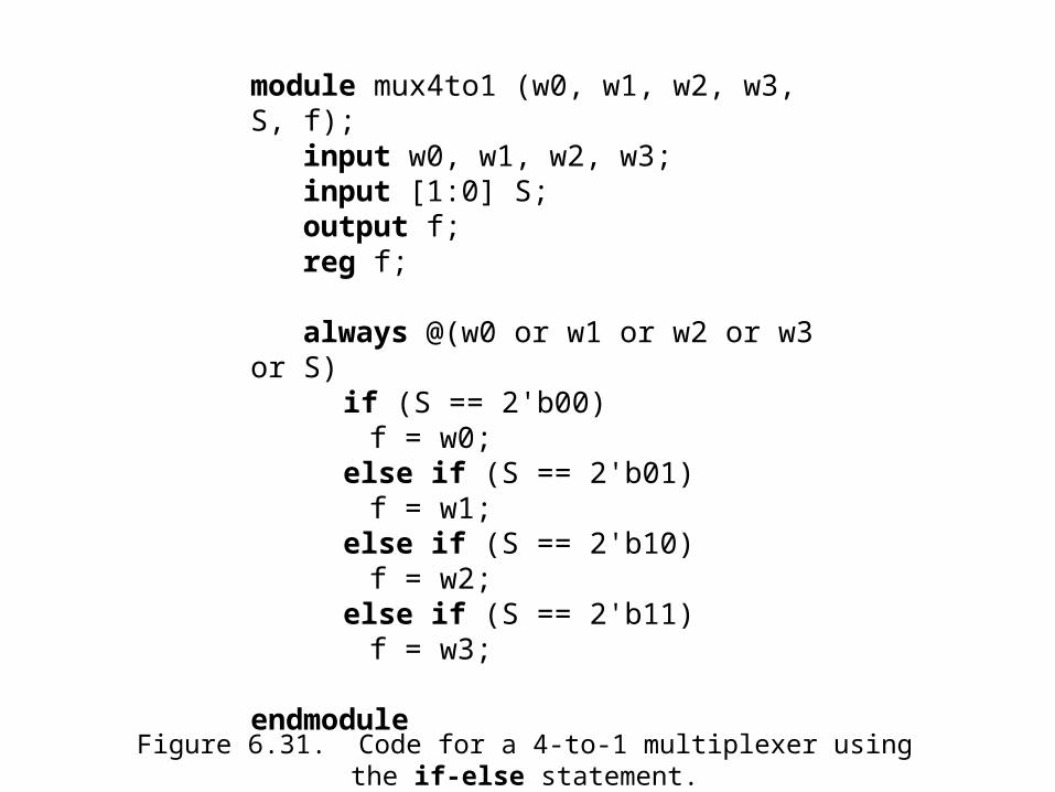
Figure 6.31. Code for a 4-to-1 multiplexer using the if-else statement.
module mux4to1 (w0, w1, w2, w3, S, f);input w0, w1, w2, w3;input [1:0] S;output f;reg f;
always @(w0 or w1 or w2 or w3 or S)if (S == 2'b00)
f = w0;else if (S == 2'b01)
f = w1;else if (S == 2'b10)
f = w2;else if (S == 2'b11)
f = w3;
endmodule
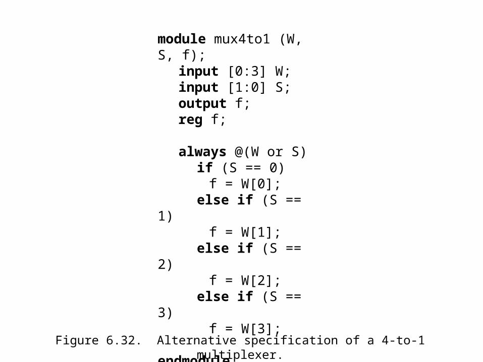
Figure 6.32. Alternative specification of a 4-to-1 multiplexer.
module mux4to1 (W, S, f);input [0:3] W;input [1:0] S;output f;reg f;
always @(W or S)if (S == 0)
f = W[0];else if (S == 1)
f = W[1];else if (S == 2)
f = W[2];else if (S == 3)
f = W[3];
endmodule

Figure 6.33. Hierarchical code for a 16-to-1 multiplexer.
module mux16to1 (W, S16, f);input [0:15] W;input [3:0] S16;output f;wire [0:3] M;
mux4to1 Mux1 (W[0:3], S16[1:0], M[0]);mux4to1 Mux2 (W[4:7], S16[1:0], M[1]);mux4to1 Mux3 (W[8:11], S16[1:0], M[2]);mux4to1 Mux4 (W[12:15], S16[1:0], M[3]);mux4to1 Mux5 (M[0:3], S16[3:2], f);
endmodule

Figure 6.34. A 4-to-1 multiplexer defined using the case statement.
module mux4to1 (W, S, f);input [0:3] W;input [1:0] S;output f;reg f;
always @(W or S)case (S)
0: f = W[0]; 1: f = W[1];
2: f = W[2];3: f = W[3];
endcase
endmodule
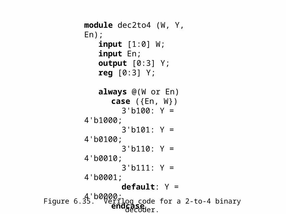
Figure 6.35. Verilog code for a 2-to-4 binary decoder.
module dec2to4 (W, Y, En);input [1:0] W;input En;output [0:3] Y;reg [0:3] Y;
always @(W or En)case ({En, W})
3'b100: Y = 4'b1000;3'b101: Y = 4'b0100;3'b110: Y = 4'b0010;3'b111: Y = 4'b0001;default: Y = 4'b0000;
endcase
endmodule
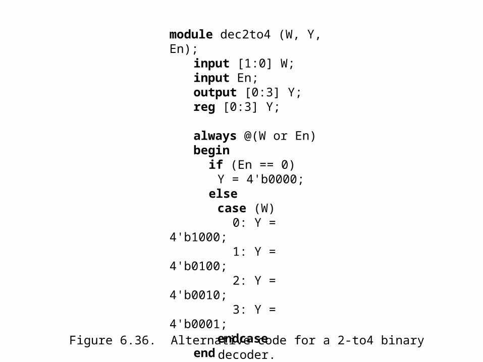
Figure 6.36. Alternative code for a 2-to4 binary decoder.
module dec2to4 (W, Y, En);input [1:0] W;input En;output [0:3] Y;reg [0:3] Y;
always @(W or En)begin
if (En == 0)Y = 4'b0000;
elsecase (W)
0: Y = 4'b1000;1: Y = 4'b0100;2: Y = 4'b0010;3: Y = 4'b0001;
endcaseend
endmodule
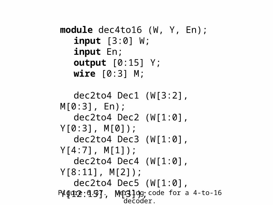
Figure 6.37. Verilog code for a 4-to-16 decoder.
module dec4to16 (W, Y, En);input [3:0] W;input En;output [0:15] Y;wire [0:3] M;
dec2to4 Dec1 (W[3:2], M[0:3], En);dec2to4 Dec2 (W[1:0], Y[0:3], M[0]);dec2to4 Dec3 (W[1:0], Y[4:7], M[1]);dec2to4 Dec4 (W[1:0], Y[8:11], M[2]);dec2to4 Dec5 (W[1:0], Y[12:15], M[3]);
endmodule

Figure 6.38. Code for a BCD-to-7-segment decoder.
module seg7 (bcd, leds);input [3:0] bcd;output [1:7] leds;reg [1:7] leds;
always @(bcd)case (bcd) //abcdefg
0: leds = 7'b1111110; 1: leds = 7'b0110000;
2: leds = 7'b1101101;3: leds = 7'b1111001;4: leds = 7'b0110011;5: leds = 7'b1011011;6: leds = 7'b1011111;7: leds = 7'b1110000;8: leds = 7'b1111111;9: leds = 7'b1111011;default: leds = 7'bx;
endcase
endmodule

Table 6.1. The functionality of the 74381 ALU.

Figure 6.39. Code that represents the functionality of the 74381 ALU chip.
// 74381 ALUmodule alu(s, A, B, F);
input [2:0] s;input [3:0] A, B;output [3:0] F;reg [3:0] F;
always @(s or A or B)case (s)
0: F = 4'b0000; 1: F = B - A;
2: F = A - B;3: F = A + B;4: F = A ^ B;5: F = A | B;6: F = A & B;7: F = 4'b1111;
endcase
endmodule
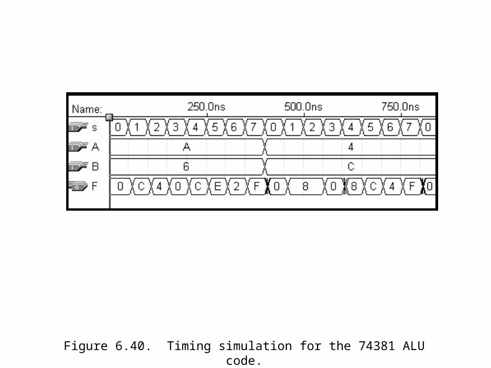
Figure 6.40. Timing simulation for the 74381 ALU code.
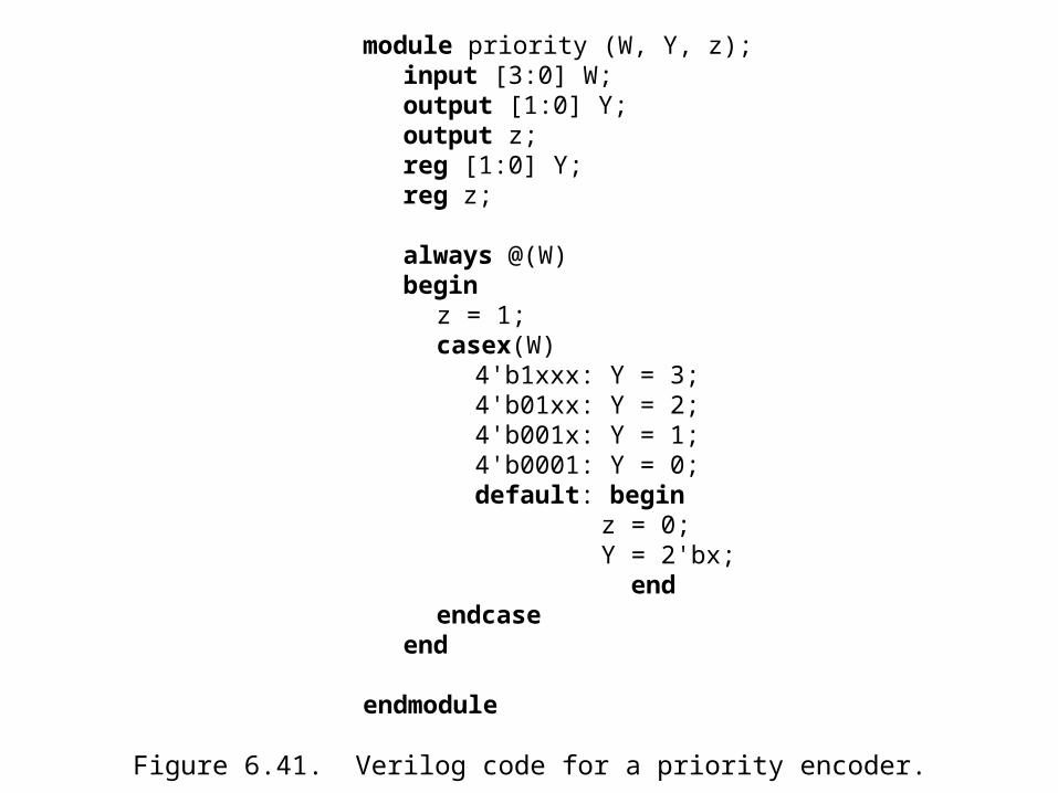
Figure 6.41. Verilog code for a priority encoder.
module priority (W, Y, z);input [3:0] W;output [1:0] Y;output z;reg [1:0] Y;reg z;
always @(W)begin
z = 1;casex(W)
4'b1xxx: Y = 3;4'b01xx: Y = 2;4'b001x: Y = 1;4'b0001: Y = 0;default: begin
z = 0;Y = 2'bx;
end endcaseend
endmodule
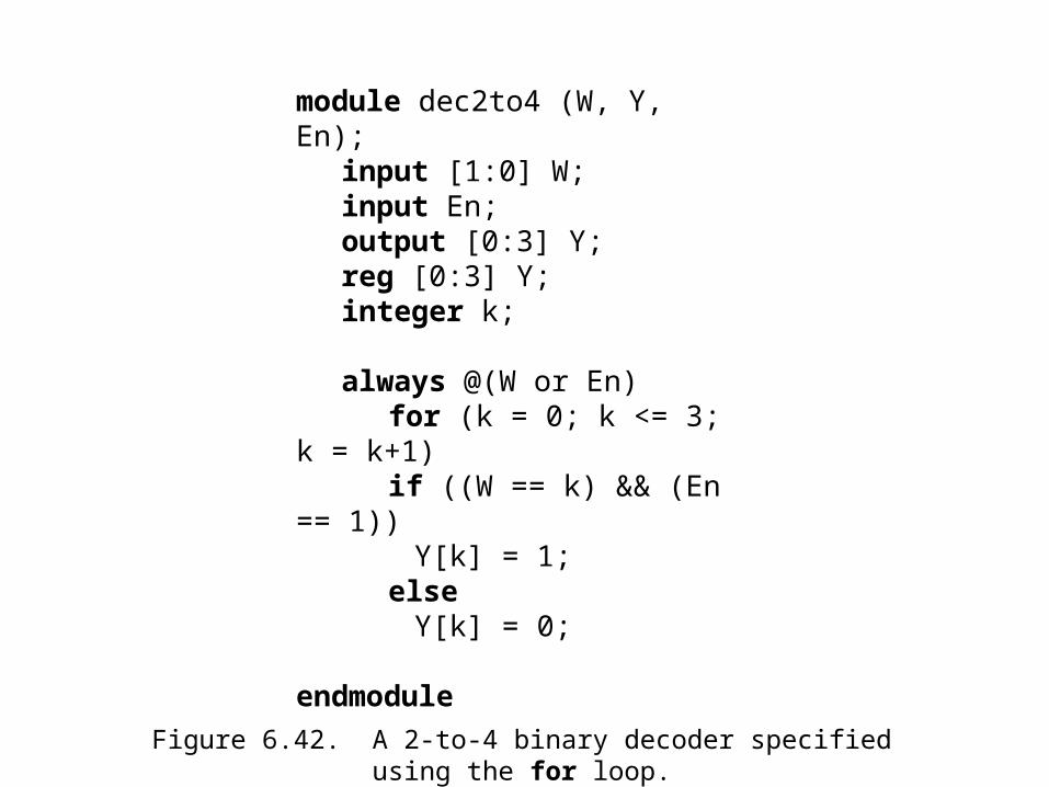
Figure 6.42. A 2-to-4 binary decoder specified using the for loop.
module dec2to4 (W, Y, En);input [1:0] W;input En;output [0:3] Y;reg [0:3] Y;integer k;
always @(W or En)for (k = 0; k <= 3; k = k+1)if ((W == k) && (En == 1))
Y[k] = 1;else
Y[k] = 0;
endmodule
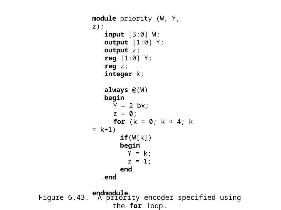
Figure 6.43. A priority encoder specified using the for loop.
module priority (W, Y, z);input [3:0] W;output [1:0] Y;output z;reg [1:0] Y;reg z;integer k;
always @(W)begin
Y = 2'bx;z = 0;for (k = 0; k < 4; k = k+1)
if(W[k])begin
Y = k;z = 1;
endend
endmodule

Table 6.2. Verilog operators.
Please see “portrait orientation” PowerPoint file for Chapter 6
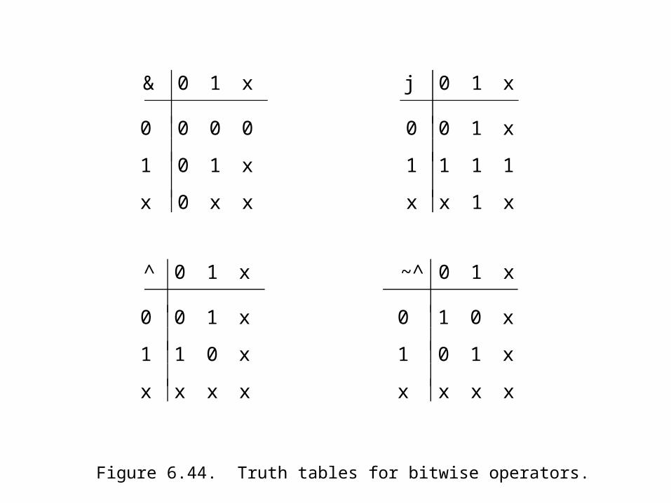
Figure 6.44. Truth tables for bitwise operators.
& 0 1 x j 0 1 x
0 0 0 0 0 0 1 x
1 0 1 x 1 1 1 1
x 0 x x x x 1 x
^ 0 1 x ~^ 0 1 x
0 0 1 x 0 1 0 x
1 1 0 x 1 0 1 x
x x x x x x x x
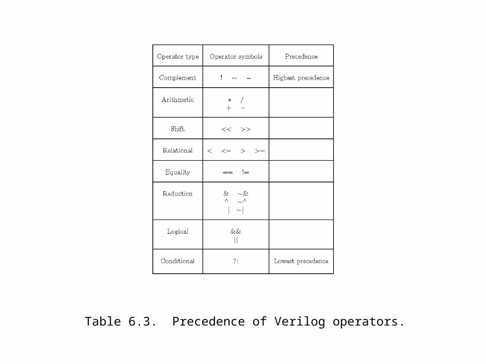
Table 6.3. Precedence of Verilog operators.

Figure 6.45. Verilog code for a four-bit comparator.
module compare (A, B, AeqB, AgtB, AltB);input [3:0] A, B;output AeqB, AgtB, AltB;reg AeqB, AgtB, AltB;
always @(A or B)begin
AeqB = 0;AgtB = 0;AltB = 0;if(A == B)
AeqB = 1;else if (A > B)
AgtB = 1;else
AltB = 1;end
endmodule
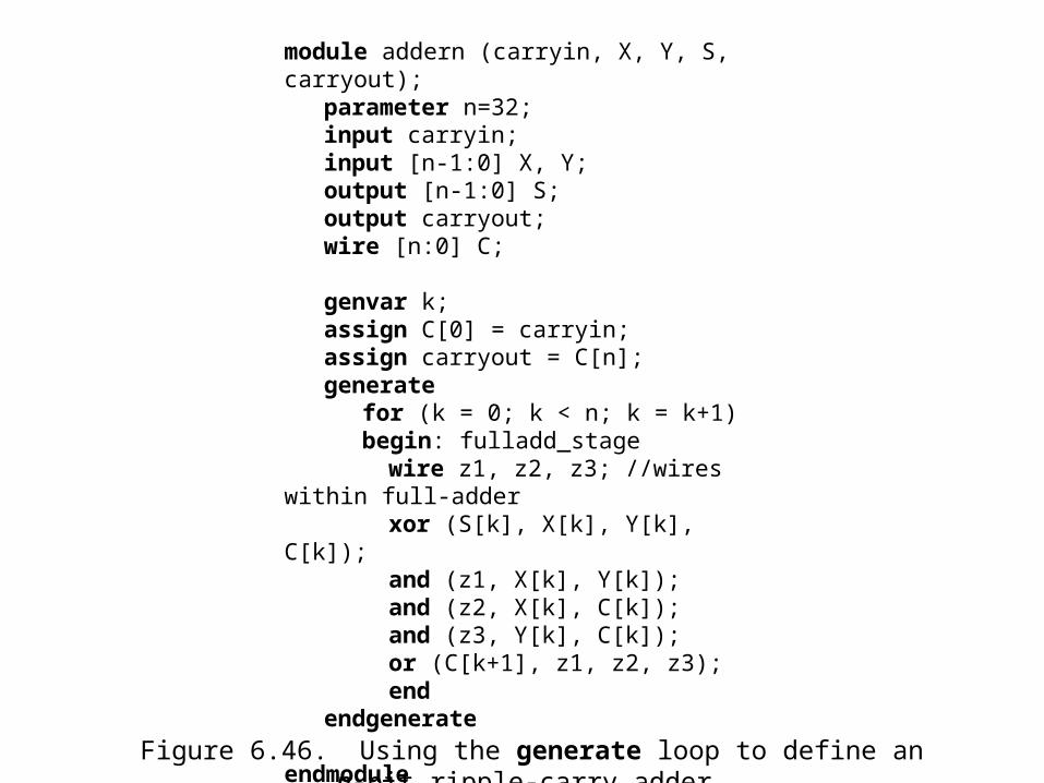
Figure 6.46. Using the generate loop to define an n-bit ripple-carry adder.
module addern (carryin, X, Y, S, carryout);parameter n=32;input carryin;input [n-1:0] X, Y;output [n-1:0] S;output carryout;wire [n:0] C;
genvar k;assign C[0] = carryin;assign carryout = C[n];generate
for (k = 0; k < n; k = k+1)begin: fulladd_stage
wire z1, z2, z3; //wires within full-adderxor (S[k], X[k], Y[k], C[k]);and (z1, X[k], Y[k]);and (z2, X[k], C[k]);and (z3, Y[k], C[k]);or (C[k+1], z1, z2, z3);
endendgenerate
endmodule
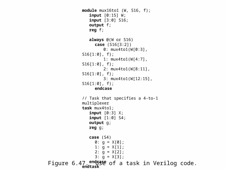
Figure 6.47. Use of a task in Verilog code.
module mux16to1 (W, S16, f);input [0:15] W;input [3:0] S16;output f;reg f;
always @(W or S16)case (S16[3:2])
0: mux4to1(W[0:3], S16[1:0], f);1: mux4to1(W[4:7], S16[1:0], f);
2: mux4to1(W[8:11], S16[1:0], f);3: mux4to1(W[12:15], S16[1:0], f);
endcase // Task that specifies a 4-to-1 multiplexertask mux4to1;
input [0:3] X;input [1:0] S4;output g;reg g;
case (S4)0: g = X[0];1: g = X[1]; 2: g = X[2];3: g = X[3];
endcaseendtask endmodule
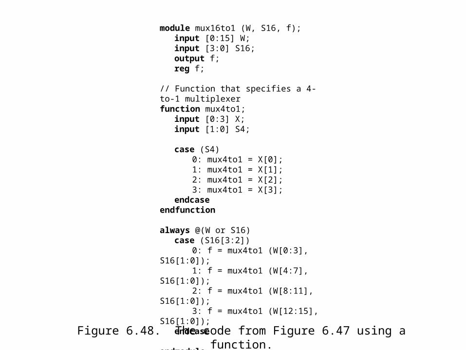
Figure 6.48. The code from Figure 6.47 using a function.
module mux16to1 (W, S16, f);input [0:15] W;input [3:0] S16;output f;reg f;
// Function that specifies a 4-to-1 multiplexerfunction mux4to1;
input [0:3] X;input [1:0] S4;
case (S4)0: mux4to1 = X[0];1: mux4to1 = X[1];2: mux4to1 = X[2];3: mux4to1 = X[3];
endcaseendfunction always @(W or S16)
case (S16[3:2])0: f = mux4to1 (W[0:3], S16[1:0]);1: f = mux4to1 (W[4:7], S16[1:0]);2: f = mux4to1 (W[8:11], S16[1:0]);3: f = mux4to1 (W[12:15], S16[1:0]);
endcase endmodule

Figure P6.1. The Actel Act 1 logic block.
i 3
i 4 i 5
i 8
f
i 2
i 6
i 1
i 7

Figure P6.2. Code for problem 6.18.
module problem61_18 (W, En, y0, y1, y2, y3) ;input [1:0]W; input En; output y0, y1, y2, y3; reg y0, y1, y2, y3;
always @ (W or En) begin
y0 = 0;y1 = 0;y2 = 0;y3 = 0;if (En)
if (W == 0) y0 = 1;else if (W == 1) y1 = 1;else if (W == 2) y2 = 1;else y3 = 1;
end
endmodule
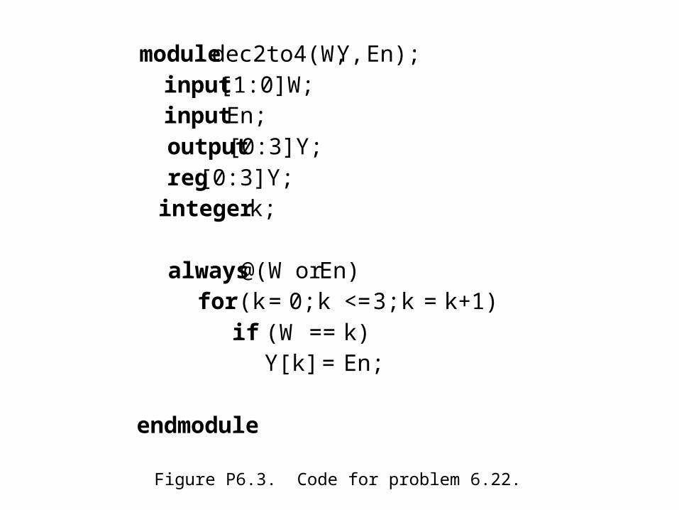
Figure P6.3. Code for problem 6.22.
module dec2to4(W, Y, En);input [1:0]W; input En; output [0:3]Y; reg [0:3]Y; integer k;
always @(W or En) for (k = 0; k <= 3; k = k+1)
if (W == k)Y[k] = En;
endmodule
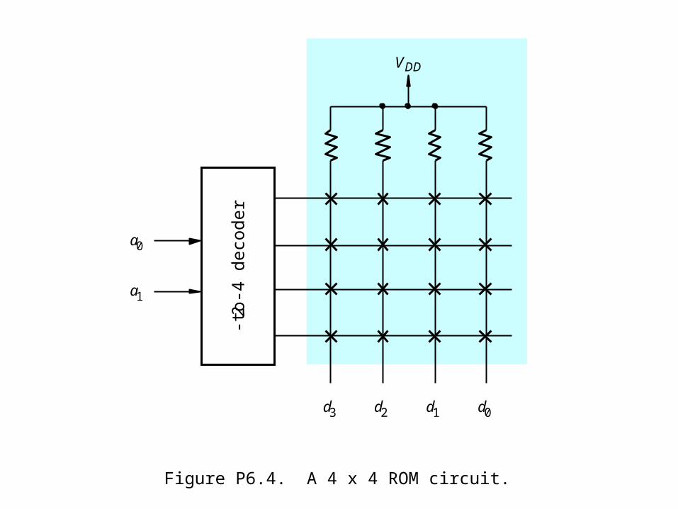
Figure P6.4. A 4 x 4 ROM circuit.
3 d 2 d 1 d 0
V DD
2
-to-4
deco
der
a 0
a 1
d


![Getting Started with SPI - Microchip Technologyww1.microchip.com/downloads/en/AppNotes/TB3215... · Bit 7 6 5 4 3 2 1 0 TWI0[1:0] SPI0[1:0] Access R/W R/W R/W R/W Reset 0 0 0 0 The](https://static.fdocuments.in/doc/165x107/5f40a0e9035c0d43b9017c11/getting-started-with-spi-microchip-bit-7-6-5-4-3-2-1-0-twi010-spi010-access.jpg)
