Emission Reduction and Assisted Combustion Strategies for ...

Field-emission-assisted approach to dry micro-electro-dischargemachining of carbon-nanotube forestsTanveer Saleh, Masoud Dahmardeh, Anas Bsoul, Alireza Nojeh, and Kenichi Takahata Citation: J. Appl. Phys. 110, 103305 (2011); doi: 10.1063/1.3663438 View online: http://dx.doi.org/10.1063/1.3663438 View Table of Contents: http://jap.aip.org/resource/1/JAPIAU/v110/i10 Published by the American Institute of Physics. Related ArticlesMicrofabricated atomic vapor cell arrays for magnetic field measurements Rev. Sci. Instrum. 82, 033111 (2011) Bianalyte mass detection with a single resonant microcantilever Appl. Phys. Lett. 94, 011901 (2009) The advanced ion-milling method for preparation of thin film using ion slicer: Application to a sample recoveredfrom diamond-anvil cell Rev. Sci. Instrum. 80, 013901 (2009) Simultaneous detection of translational and angular displacements of micromachined elements Appl. Phys. Lett. 91, 221908 (2007) Global dynamics of low immersion high-speed milling Chaos 14, 1069 (2004) Additional information on J. Appl. Phys.Journal Homepage: http://jap.aip.org/ Journal Information: http://jap.aip.org/about/about_the_journal Top downloads: http://jap.aip.org/features/most_downloaded Information for Authors: http://jap.aip.org/authors
Downloaded 16 Dec 2011 to 137.82.251.158. Redistribution subject to AIP license or copyright; see http://jap.aip.org/about/rights_and_permissions

Field-emission-assisted approach to dry micro-electro-discharge machiningof carbon-nanotube forests
Tanveer Saleh,1,2 Masoud Dahmardeh,1 Anas Bsoul,1,3 Alireza Nojeh,1,a)
and Kenichi Takahata1,a)
1Department of Electrical and Computer Engineering, University of British Columbia, Vancouver,BC V6T 1Z4, Canada2FARCAMT, Industrial Engineering Department, College of Engineering, King Saud University,Riyadh 11421, Saudi Arabia3Department of Computer Engineering, Jordan University of Science and Technology, Irbid, Jordan
(Received 10 July 2011; accepted 27 October 2011; published online 29 November 2011)
This work investigates dry micro-electro-discharge machining (lEDM) of vertically aligned carbon
nanotube (CNT) forests that are used as cathodes in the process, as opposed to conventional lEDM
where the material to be machined forms the anode, toward achieving higher precision in the
patterned microstructures. The new configuration with the reversed polarity is observed to generate
higher discharge currents in the process, presumably due to effective field-emission from CNTs. This
effect allows the process to be performed at very low discharge energies, approximately 80� smaller
than in the conventional normal-polarity case, with the machining voltage and tolerance down to
10 V and 2.5 lm, respectively, enabling high-precision high-aspect-ratio micropatterning in the
forests. The new approach is also demonstrated to make the process faster, cleaner, and more stable
than conventional processing. Spectroscopic analyses of the forests processed by reverse lEDM
show no evidence of significant crystalline deterioration or contamination in the CNTs. VC 2011American Institute of Physics. [doi:10.1063/1.3663438]
I. INTRODUCTION
Carbon nanotubes (CNTs) have highly attractive
mechanical, electrical, optical, and thermal properties.1–5
Densely packed, vertically aligned CNTs are commonly
referred to as CNT forests and have many potential engineer-
ing applications in the field of micro-electro-mechanical sys-
tems (MEMS),6 micro-chip heat sinks,7 field-emitters,8–10
gas sensors,11 photovoltaics,12 fuel cells,13 and synthetic uni-
directional adhesive tapes.14 It is very important to pattern
CNT forests to make them useful for many of the above
applications. The formation of patterned CNT forests has
widely been conducted through selective growth of the for-
ests by chemical vapor deposition (CVD) on pre-patterned
catalyst on the substrate. However, this technique is limited
to producing two-dimensional patterns with uniform height.
Micropatterning of three-dimensional, free-form structures
with high aspect ratios in pure CNT forests was recently
demonstrated using a process based on micro-electro-dis-
charge machining (lEDM).15,16 Dry air was used as the
dielectric medium in the process, instead of the dielectric liq-
uid used in typical lEDM, as the forest structures patterned
in liquid are drastically modified when the structures are
dried because of the capillary effect.15 The optimal machin-
ing condition was observed at the discharge voltage of 30 V.
This technique was further investigated in Refs. 16 and 17.
These studies revealed a possible removal mechanism of
CNT forests in dry lEDM, suggesting that the process is
essentially oxygen plasma etching rather than the conven-
tional, direct thermal removal (evaporation and melting) pro-
cess. The role of oxygen in the process was also investigated
and it was reported that air was an optimal medium for
lEDM of CNT forests. The EDM condition at 60 V and
10 pF was effective in creating needle-like microstructure
arrays in CNT forests.16 The machining tolerance, or the dis-
charge gap clearance between a forest and the lEDM elec-
trode, was reported to be 10 lm or more, substantially larger
than typical values (of one to a few micrometers) involved in
standard lEDM with dielectric liquid. Toward achieving higher
precision and nano-scale removal in dry lEDM of CNT forests,
it is essential to minimize the discharge voltage and the dis-
charge gap while achieving effective removal of CNTs.
In typical EDM (including lEDM), the workpiece and
the electrode are generally arranged to be the anode and the
cathode, respectively, as this polarity usually results in effi-
cient material removal with small electrode wear. To the
best of the authors’ knowledge, all previous studies on
carbon-nanofiber or CNT-forest lEDM have used this con-
ventional polarity, i.e., the carbon material has served as the
anode while the tungsten electrode has been used as the
cathode.15–17 However, the effect of the polarity of the CNT
forest on the EDM removal of the material has not been stud-
ied. Because of their extremely small tips with nanometer
radii and high aspect ratios, CNTs are known to significantly
enhance an applied electric field and thus have excellent
electron emission properties. In fact, CNT cathodes were
reported to reduce gas breakdown voltage while increasing
the discharge current compared to tungsten cathodes;18
although the set-up and the ranges of the breakdown voltage
a)Authors to whom correspondence should be addressed. Electronic mail:
[email protected] and [email protected].
0021-8979/2011/110(10)/103305/7/$30.00 VC 2011 American Institute of Physics110, 103305-1
JOURNAL OF APPLIED PHYSICS 110, 103305 (2011)
Downloaded 16 Dec 2011 to 137.82.251.158. Redistribution subject to AIP license or copyright; see http://jap.aip.org/about/rights_and_permissions
and current reported are different (one to two orders of mag-
nitude) from those involved in lEDM, the above suggests
that the use of reverse polarity in lEDM of CNT forests
could be effective in lowering the discharge voltage and gap
clearance (for higher precision) as well as increasing the dis-
charge current (for effective CNT removal) in the process.
To explore this hypothesis, the present work investigates
reverse-polarity lEDM of pure CNT forests in dry air exper-
imentally. The characteristics of reverse lEDM for CNT for-
ests and the patterned structures are studied to reveal various
advantages over the conventional process with the normal
polarity, achieving higher precision in the forest patterning
process including that for high-aspect-ratio geometries.
II. EXPERIMENTAL SET-UP
The CNT forest samples used in this study were grown
on highly doped silicon substrates (h100i n-type, resistivity
0.008-0.015 X�cm) using an atmospheric-pressure CVD sys-
tem. The samples were prepared as follows: First, a 10-nm-
thick layer of aluminum was evaporated on the silicon wafer.
Subsequently, a 1-nm-thick layer of iron was deposited. The
CNT growth was performed by placing the sample on a piece
of a lightly doped Si wafer that served as the resistive heater
(CNT growth zone) in the reaction tube of the system. A pre-
heater was used to heat up the gas at �30 cm before reaching
the growth zone. In a typical growth process, after loading
the sample, the pre-heater’s temperature was ramped up
from room temperature to 850 �C in 20 min while maintain-
ing a flow of 400 sccm of argon. Then the silicon heater was
turned on to maintain the temperature of the sample at
�750 �C for 2 min. The sample was annealed for 5 min under
140 sccm of argon and 400 sccm of hydrogen. Subsequently,
flow rates of 140 sccm of ethylene, 400 sccm of hydrogen,
and 100 sccm of argon were used for 15 min for the CNT
growth. The growth was ended by turning off the silicon
heater and all the gas flows except for 400 sccm of argon for
about 20 min to cool the pre-heater down to room tempera-
ture. This process yielded forests of vertically aligned multi-
walled CNTs with lengths of up to several 100’s of lm.
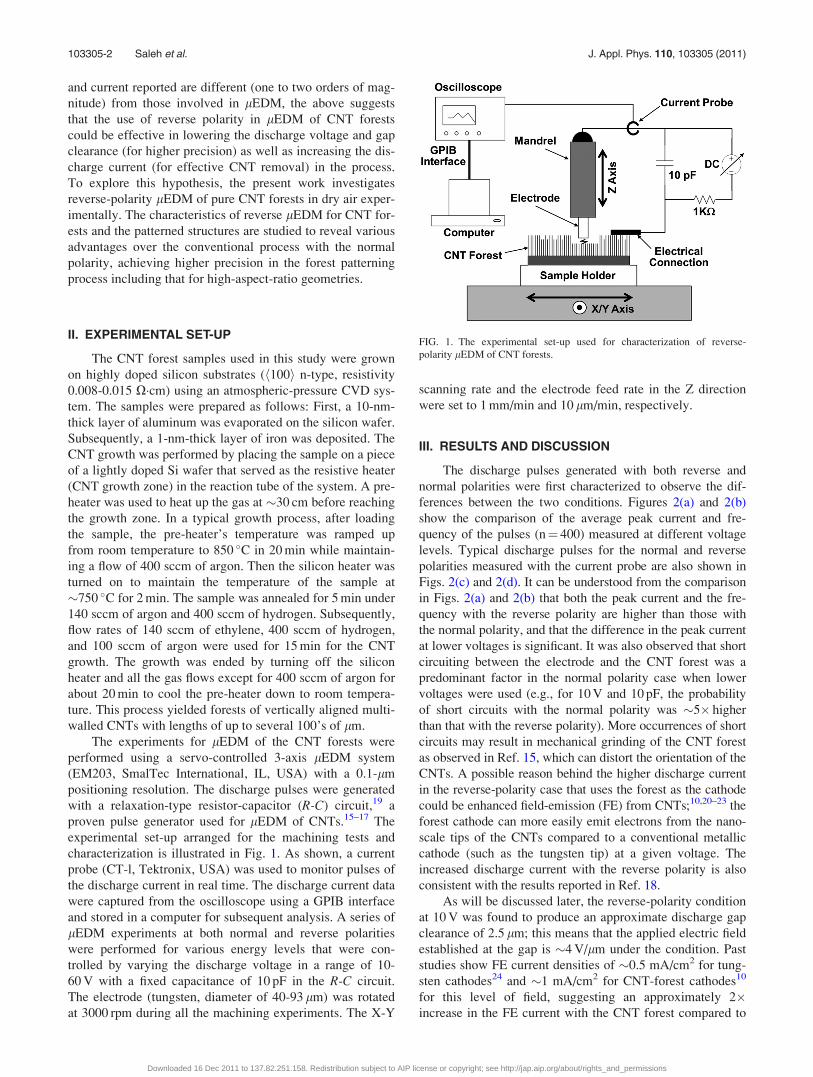
The experiments for lEDM of the CNT forests were
performed using a servo-controlled 3-axis lEDM system
(EM203, SmalTec International, IL, USA) with a 0.1-lm
positioning resolution. The discharge pulses were generated
with a relaxation-type resistor-capacitor (R-C) circuit,19 a
proven pulse generator used for lEDM of CNTs.15–17 The
experimental set-up arranged for the machining tests and
characterization is illustrated in Fig. 1. As shown, a current
probe (CT-l, Tektronix, USA) was used to monitor pulses of
the discharge current in real time. The discharge current data
were captured from the oscilloscope using a GPIB interface
and stored in a computer for subsequent analysis. A series of
lEDM experiments at both normal and reverse polarities
were performed for various energy levels that were con-
trolled by varying the discharge voltage in a range of 10-
60 V with a fixed capacitance of 10 pF in the R-C circuit.
The electrode (tungsten, diameter of 40-93 lm) was rotated
at 3000 rpm during all the machining experiments. The X-Y
scanning rate and the electrode feed rate in the Z direction
were set to 1 mm/min and 10 lm/min, respectively.
III. RESULTS AND DISCUSSION
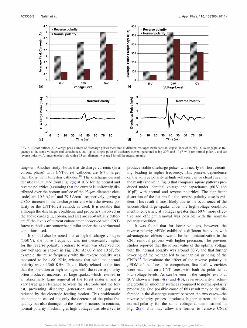
The discharge pulses generated with both reverse and
normal polarities were first characterized to observe the dif-
ferences between the two conditions. Figures 2(a) and 2(b)
show the comparison of the average peak current and fre-
quency of the pulses (n¼ 400) measured at different voltage
levels. Typical discharge pulses for the normal and reverse
polarities measured with the current probe are also shown in
Figs. 2(c) and 2(d). It can be understood from the comparison
in Figs. 2(a) and 2(b) that both the peak current and the fre-
quency with the reverse polarity are higher than those with
the normal polarity, and that the difference in the peak current
at lower voltages is significant. It was also observed that short
circuiting between the electrode and the CNT forest was a
predominant factor in the normal polarity case when lower
voltages were used (e.g., for 10 V and 10 pF, the probability
of short circuits with the normal polarity was �5� higher
than that with the reverse polarity). More occurrences of short
circuits may result in mechanical grinding of the CNT forest
as observed in Ref. 15, which can distort the orientation of the
CNTs. A possible reason behind the higher discharge current
in the reverse-polarity case that uses the forest as the cathode
could be enhanced field-emission (FE) from CNTs;10,20–23 the
forest cathode can more easily emit electrons from the nano-
scale tips of the CNTs compared to a conventional metallic
cathode (such as the tungsten tip) at a given voltage. The
increased discharge current with the reverse polarity is also
consistent with the results reported in Ref. 18.
As will be discussed later, the reverse-polarity condition
at 10 V was found to produce an approximate discharge gap
clearance of 2.5 lm; this means that the applied electric field
established at the gap is �4 V/lm under the condition. Past
studies show FE current densities of �0.5 mA/cm2 for tung-
sten cathodes24 and �1 mA/cm2 for CNT-forest cathodes10
for this level of field, suggesting an approximately 2�increase in the FE current with the CNT forest compared to
FIG. 1. The experimental set-up used for characterization of reverse-
polarity lEDM of CNT forests.
103305-2 Saleh et al. J. Appl. Phys. 110, 103305 (2011)
Downloaded 16 Dec 2011 to 137.82.251.158. Redistribution subject to AIP license or copyright; see http://jap.aip.org/about/rights_and_permissions
tungsten. Another study shows that discharge currents (in a
corona phase) with CNT-forest cathodes are 6-7� larger
than those with tungsten cathodes.18 The discharge current
densities calculated from Fig. 2(a) at 10 V for the normal and
reverse polarities (assuming that the current is uniformly dis-
tributed over the bottom surface of the 93-lm-diameter elec-
trode) are 10.3 A/cm2 and 29.5 A/cm2, respectively, giving a
2.86� increase in the discharge current when the reverse po-
larity or the CNT-forest cathode is used. It is notable that
although the discharge conditions and properties involved in
the above cases (FE, corona, and arc) are substantially differ-
ent,25 the levels of current enhancement observed with CNT-
forest cathodes are somewhat similar under the experimental
conditions used.
It should also be noted that at high discharge voltages
(>50 V), the pulse frequency was not necessarily higher
for the reverse polarity, contrary to what was observed for
low voltages as shown in Fig. 2(b). At 60 V and 10 pF, for
example, the pulse frequency with the reverse polarity was
measured to be �90 KHz, whereas that with the normal
polarity was �1360 KHz. This is likely related to the fact
that the operation at high voltages with the reverse polarity
often produced uncontrolled large sparks, which resulted in
an abnormally large removal of the forest material and a
very large gap clearance between the electrode and the for-
est, preventing discharge generation until the gap was
reduced by the electrode feeding motion. This problematic
phenomenon caused not only the decrease of the pulse fre-
quency but also damages to the forest structure. In contrast,
normal-polarity machining at high voltages was observed to
produce stable discharge pulses with nearly no short circuit-
ing, leading to higher frequency. This process dependence
on the voltage polarity at high voltages can be clearly seen in
the results shown in Fig. 3 that compares square patterns pro-
duced under identical voltage and capacitance (60 V and
10 pF) with normal and reverse polarities. The significant
distortion of the pattern for the reverse-polarity case is evi-
dent. This result is most likely due to the occurrence of the
uncontrolled large sparks under the high-voltage condition
mentioned earlier; at voltages greater than 50 V, more effec-
tive and efficient removal was possible with the normal-
polarity condition.
It was found that for lower voltages, however, the
reverse-polarity lEDM exhibited a different behavior, with
advantageous effects towards further miniaturization in the
CNT removal process with higher precision. The previous
studies reported that the lowest value of the optimal voltage
with the normal polarity was around 30 V, and that further
lowering of the voltage led to mechanical grinding of the
CNTs.15 To evaluate the effect of the reverse polarity in
lEDM of the forest for comparison, first shallow cavities
were machined on a CNT forest with both the polarities at
low-voltage levels. As can be seen in the sample results at
20 V shown in Figs. 4(a) and 4(b), reverse-polarity machin-
ing produced smoother surfaces compared to normal-polarity
processing. One possible cause of this result may be the dif-
ference in the discharge current between the two cases—the
reverse-polarity process produces higher current than the
normal-polarity for the same voltage as demonstrated in
Fig. 2(a). This may allow the former to remove CNTs
FIG. 2. (Color online) (a) Average peak current of discharge pulses measured at different voltages (with constant capacitance of 10 pF), (b) average pulse fre-
quency at the same voltages and capacitance, and typical single pulse of discharge current generated using 20 V and 10 pF with (c) normal polarity and (d)
reverse polarity. A tungsten electrode with a 93-lm diameter was used for all the measurements.
103305-3 Saleh et al. J. Appl. Phys. 110, 103305 (2011)
Downloaded 16 Dec 2011 to 137.82.251.158. Redistribution subject to AIP license or copyright; see http://jap.aip.org/about/rights_and_permissions

effectively, whereas the latter suffers from insufficient re-
moval because of smaller discharge currents, possibly caus-
ing mechanical abrasion of the forest. The above effect was
further verified with deeper patterning with both polarities,
in a similar manner as that described in Fig. 3 but at 10 V
(with 10 pF) in this case. The results in Figs. 4(c) and 4(d)
indicate that the reverse-polarity process produced sharper,
smoother, and cleaner microstructures compared to the
normal-polarity case. Moreover, the patterns created with the
reverse polarity exhibited a narrower width in the machined
grooves compared to those with the normal polarity even
though identical electrode and machining conditions were
used. From the dimensions shown in Fig. 4, as well as the di-
ameter (93 lm) of the electrode used, the discharge gap
clearance is calculated to be 7.5 lm for the normal polarity,
whereas for the reverse polarity it is 2.5 lm, which is
3� smaller (and shows a �4� improvement over the previ-
ous result reported in Ref. 15). This means that reverse
lEDM enables much tighter tolerances and higher precision
in CNT forest patterning.
Machining stability is another important aspect of
lEDM processing of CNT forests. In the process, electrode
feeding is feedback controlled so that when a short circuit is
detected, the Z stage retracts the electrode upward until the
FIG. 3. Scanning electron microscope
(SEM) images of micropatterns mac-
hined in a CNT forest using 60 V and
10 pF with (a) normal polarity and (b)
reverse polarity. Each pattern was cre-
ated by scanning a rotating electrode
along a square shape (200 lm� 200 lm)
in the X-Y plane with continuous feed-
ing of the electrode in the Z direction.
FIG. 4. The upper two SEM images
show shallow cavities machined in a
CNT forest using 20 V and 10 pF with
(a) normal polarity and (b) reverse polar-
ity. The lower two SEM images show
micropatterns machined in a CNT forest
using 10 V and 10 pF with (c) normal
polarity and (d) reverse polarity, for a
depth of 40 lm with 1-lm-step electrode
feeding in the Z direction. The images
in (c) and (d) also show close-up views
of the microstructures created in the
cavities.
103305-4 Saleh et al. J. Appl. Phys. 110, 103305 (2011)
Downloaded 16 Dec 2011 to 137.82.251.158. Redistribution subject to AIP license or copyright; see http://jap.aip.org/about/rights_and_permissions

circuit is opened and then moves the electrode downward to
resume its feeding and the machining process. The process
becomes unstable and slow if many short circuits occur dur-
ing the process because of frequent up/down motion of the Z
axis. It was observed that reverse-polarity machining at low
voltages was consistently more stable than normal-polarity
machining for CNT forests. This tendency can be seen in
Fig. 5 that plots the electrode position on the Z axis during
each of the machining processes conducted under the same
conditions except for the voltage polarity. It is clear from the
graph that the normal-polarity case produced frequent short
circuits that led to ripples in the electrode motion, whereas
the reverse-polarity case resulted in much more stable and
faster electrode feeding or removal of the CNTs. For this
particular machining condition, the total machining time
with the reverse polarity was approximately 60% shorter
than the time with the normal polarity.
Another interesting observation is that reverse-polarity
machining (at low voltages) produced very small or almost
no debris, leading to highly clean surfaces after the machin-
ing as can be seen in Fig. 4(d). In contrast, as reported in
Ref. 15, normal-polarity machining produced a substantial
amount of debris that was left on the machined surfaces
[Fig. 4(c)]. It was also observed that the debris accumulated
on and stuck to the electrode surfaces, increasing the effec-
tive diameter of the electrode in a random and non-uniform
manner. In reverse lEDM, the forest is the cathode and thus
not subject to electron bombardment (leading to the conven-
tional thermal removal) in principle; therefore, CNT removal
is expected to be almost entirely due to oxygen plasma etch-
ing that can decompose CNTs into volatile products, forming
virtually no debris. With the normal-polarity condition, in
contrast, the forest is the anode that is bombarded by elec-
trons during the process and may be subject to some level of
thermal removal where parts of the CNTs are melted and
blown by pressure waves induced by the intense heat that the
pulsed discharge arc produces, leaving resolidified carbon
debris on the workzone and the electrode. A single MWCNT
was reported to be heated up to 2000 K due to emitting a FE
current of 1 lA;26 this self-heating effect of CNTs may need
to be considered with respect to the removal process. How-
ever, in the present case, the current passed through a single
CNT by a discharge pulse is estimated to be significantly
lower, e.g., �300 pA for the 10 V condition that involves an
average peak discharge current of 2 mA [Fig. 2(a)] consider-
ing the typical CNT density of �1011/cm2 observed in the
forest samples and the electrode diameter of 93 lm used in
the experiment. Moreover, the lEDM process uses pulsed
currents as opposed to DC current involved in Ref. 26.
Therefore, the impact of the self-heating effect on the re-
moval process is likley minimal under the relevant machin-
ing condition.
A key factor for high-aspect-ratio patterning in CNT
forets is debris removal.15 It is also essential to maintain the
electrode surfaces free from debris accumulation that
degrades the machining precision and can destroy the high-
aspect-ratio microstructures produced during the process. It
was observed in the present study that the use of a relatively
high discharge energy (e.g., 60 V and 10 pF) was effective in
reducing debris generation under the normal polarity condi-
tion (in Ref. 16, needle-like microstructures were created
with this method), which could be due to the enhancement of
the oxygen-plasma etching phenomenon; however, the use
of higher voltages tends to cause lower tolerance and more
roughness in the machined surfaces. All these issues may be
effectively addressed through reverse lEDM because of its
cleanness and the possibililty of usage of low voltages as dis-
cussed above. The effectiveness of reverse lEDM in high-
aspect-ratio micromachining of CNT forests was evaluated
FIG. 5. (Color online) Electrode positions on the Z axis tracked in real time
during machining with normal and reverse polarities, both using 10 V and
10 pF. In both cases, the electrode was scanned along a square shape
(100 lm� 100 lm) in the X-Y plane with 1-lm-step feeding in the Z direc-
tion until reaching a depth of 40 lm.
FIG. 6. SEM images of patterned high-
aspect-ratio microstructures: (a) a cone
shaped with normal polarity at 60 V and
10 pF by scanning a tapered electrode
along a circular orbit with 90 lm diame-
ter while feeding the electrode in the Z
direction with 1-lm steps; (b) a cone
shaped with reverse polarity at 10 V and
10 pF under the same scanning/feeding
conditions as in (a). The height of both
cones is 120 lm.
103305-5 Saleh et al. J. Appl. Phys. 110, 103305 (2011)
Downloaded 16 Dec 2011 to 137.82.251.158. Redistribution subject to AIP license or copyright; see http://jap.aip.org/about/rights_and_permissions

by patterning conical microstructuers with the conventional
normal-polarity condition at 60 V as well as with the
reverse-polarity condition at 10 V (both with 10 pF) using a
tapered cyrindlical electrode. As can be seen from the results
in Fig. 6, reverse lEDM achieved finer structures with
higher aspect ratios and smoother surfaces, demonstrating its
effectiveness with low discharge energies for high-aspect-ra-
tio patterning in CNT forests. Since the discharge energy is
equal to CV2/2, where C is the capacitance of the R-C circuit
(ignoring parasitics) and V is the voltage, the above electrical
conditions and results suggest that the discharge energy
involved in the reverse-polarity case is 0.5 nJ, 36� smaller
than the energy for the normal-polarity case (and �80�smaller than the energy used for the high-aspect-ratio
machining reported in Ref. 16), and that reverse-polarity
lEDM enables proper CNT removal using such low dis-
charge energies.
Energy-dispersive X-ray spectroscopy (EDX) of the
CNT forest surfaces machined at 10 V and 10 pF [Fig. 7]
indicated no detectable signals relevant to the electrode ma-
terial (tungsten) with both the reverse and normal polarities,
suggesting that the use of the reverse polarity involves almost
zero consumption of the electrode and thus does not cause
contamination of the processed forest surfaces with the elec-
trode material. A high level of silicon detected in addition to
carbon is most likely due to the presence of the substrate
below the forest. These observations are also consistent with
the previous results.15 (Although the data shows a larger
silicon peak for the normal-polarity case as seen in Fig. 7, we
have not observed a similar behavior in other samples stud-
ied. Therefore, we believe this could be related to the non-
uniformity in the initial thickness of the forest that has led to
a difference in the forest thickness left after the removal,
rather than an effect related to polarity.) Raman spectroscopy
provided no evidence of significant ID/IG ratio reduction,
i.e., increased defects in the CNTs processed with either po-
larity under different conditions [Fig. 8].
IV. CONCLUSIONS
The effect of using reverse polarity in lEDM was inves-
tigated for micropatterning of pure CNT forests. It was found
that the process with the reverse-polarity condition increased
the discharge current, possibly because of the field-emission
properties of CNTs that serve as the cathode in reverse
lEDM. This concept was utilized to achieve lEDM of CNT
forests at lower machining voltages or discharge energies
compared to the previously reported conditions. The struc-
tures machined with reverse lEDM at low voltages were
found to have higher precision and smoother and cleaner
surfaces with almost no debris compared with those produced
using conventional, normal-polarity processing. Reverse
lEDM was also found to enable more stable and faster
machining of the forests. Raman and EDX analyses revealed
that reverse lEDM did not cause significant crystalline
defects in the processed CNTs and contamination of the forest
surfaces with the electrode element, respectively.
ACKNOWLEDGMENTS
The authors thank Mohamed Sultan Mohamed Ali for
his assistance in use of the lEDM system. We also thank
Mehran Vahdani Moghaddam and Parham Yaghoobi for as-
sistance with the nanotube growth process. This work was
partially supported by the Natural Sciences and Engineering
Research Council of Canada, the Canada Foundation for
Innovation, and the British Columbia Knowledge Develop-
ment Fund. K. Takahata is supported by the Canada Research
Chairs program. A. Bsoul acknowledges financial support
from the Jordan University of Science and Technology.
1M. M. J. Treacy, T. W. Ebbesen, and J. M. Gibson, Nature 381, 678
(1996).2J. P. Lu, Phys. Rev. Lett. 79, 1297 (1997).3K. Hsieh, T. Tsai, D. Wan, H. Chen, and N. Tai, ACS Nano 4, 1327
(2010).
FIG. 7. EDX analysis results for the CNT-forest surfaces machined with (a)
normal polarity and (b) reverse polarity.
FIG. 8. (Color online) Raman ID/IG ratios for a forest sample machined at
30 V with different capacitor values.
103305-6 Saleh et al. J. Appl. Phys. 110, 103305 (2011)
Downloaded 16 Dec 2011 to 137.82.251.158. Redistribution subject to AIP license or copyright; see http://jap.aip.org/about/rights_and_permissions

4Z. Yang, L. Ci, J. A. Bur, S. Lin, and P. M. Ajayan, Nano Lett. 8, 446 (2008).5N. Hamada, S. Sawada, and A. Oshiyama, Phys. Rev. Lett. 68, 1579 (1992).6Y. Hayamizu, T. Yamada, K. Mizuno, R. C. Davis, D. N. Futaba,
M. Yumura, and K. Hata, Nat. Nanotechnol. 3, 289 (2008).7K. Kordas, G. Toth, P. Moilanen, M. Kumpumaki, J. Vahakangas, A. Uusi-
maki, R. Vajtai, and P. M. Ajayan, Appl. Phys. Lett. 90, 123105 (2007).8M. Chhowalla, C. Ducati, N. L. Rupesinghe, K. B. K. Teo, and
G. A. J. Amaratunga, Appl. Phys. Lett. 79, 2079 (2001).9T. Y. Tsai, C. Y. Lee, N. H. Tai, and W. H. Tuan, Appl. Phys. Lett. 95,
013107 (2009).10S. Fan, M. G. Chapline, N. R. Franklin, T. W. Tombler, A. M. Cassell, and
H. Dai, Science 283, 512 (1999).11Y. Jiang, P. Wang, and L. Lin, 24th IEEE International Conference Micro
Electro Mechanical Systems, MEMS 2011, 23-27 January 2011 (Cancun,
Mexico, 2011), pp. 396–399.12J. Yang and D.-J. Liu, Carbon 45, 2843 (2007).13J. Flicker and J. Ready, J. Appl. Phys. 103, 113110 (2008).14L. Ge, S. Sethi, L. Ci, P. M. Ajayan, and A. Dhinojwala, Proc. Natl. Acad.
Sci. 104, 10792 (2007).15W. Khalid, M. S. Mohamed Ali, M. Dahmardeh, Y. Choi, P. Yaghoobi,
A. Nojeh, and K. Takahata, Diamond Relat. Mater. 19, 1405 (2010).
16M. Dahmardeh, W. Khalid, M. S. Mohamed Ali, Y. Choi, P. Yaghoobi, A.
Nojeh, and K. Takahata, 24th IEEE International Conference on MicroElectro Mechanical Systems (MEMS 2011) (Cancun, Mexico, 2011),
pp. 272–275.17M. Dahmardeh, A. Nojeh, and K. Takahata, J. Appl. Phys. 109, 093308
(2011).18B. Liang, A. Ogino, and M. Nagatsu, J. Phys. D: Appl. Phys. 43, 275202
(2010).19M. P. Jahan, Y. S. Wong, and M. Rahman, J. Mater. Process. Technol.
209, 1706 (2009).20W. A. de Heer, A. Chatelain, and D. Ugarte, Science 270, 1179 (1995).21J.-M. Bonard, M. Croci, C. Klinke, R. Kurt, O. Noury, and N. Weiss,
Carbon 40, 1715 (2002).22P. G. Collins and A. Zettl, Appl. Phys. Lett. 69, 1969 (1996).23Y. Saito, ed. Carbon Nanotube and Related Field-Emitters—
Fundamentals and Applications (Wiley-VCH, 2010), p. 95.24K. Sun, J. Y. Lee, B. Li, W. Liu, 1. C. Miao, Y. H. Xie, X. Wei, and
T. P. Russell, J. Appl. Phys. 108, 036102 (2010).25H. C. Miller, IEEE Trans. Elec. Insul. 25, 765 (1990).26S. T. Purcell, P. Vincent, C. Journet, and V. T. Binh, Phys. Rev. Lett. 88,
105502 (2002).
103305-7 Saleh et al. J. Appl. Phys. 110, 103305 (2011)
Downloaded 16 Dec 2011 to 137.82.251.158. Redistribution subject to AIP license or copyright; see http://jap.aip.org/about/rights_and_permissions