FH-P6600R_P6600 (CRT2502)
116
PIONEER CORPORATION 4-1, Meguro 1-Chome, Meguro-ku, Tokyo 153-8654, Japan PIONEER ELECTRONICS SERVICE INC. P.O.Box 1760, Long Beach, CA 90801-1760 U.S.A. PIONEER ELECTRONIC N.V. Haven 1087 Keetberglaan 1, 9120 Melsele, Belgium PIONEER ELECTRONICS ASIACENTRE PTE.LTD. 253 Alexandra Road, #04-01, Singapore 159936 C PIONEER CORPORATION 2000 K-ZZU. MAY 2000 Printed in Japan ORDER NO. CRT2502 MULTI-CD/MD CONTROL DSP HIGH POWER CD CASSETTE PLAYER WITH RDS TUNER FH-P6600R EW Service Manual FH-P6600R/EW - This service manual should be used together with the following manual(s): Model No. Order No. Mech. Module Remarks CX-1011 CRT2406 3L Cassette Mech. Module:Circuit Description, Mech.Description, Disassembly CX-958 CRT2423 S8.1 CD Mech. Module:Circuit Description, Mech.Description, Disassembly CONTENTS 1. SAFETY INFORMATION ............................................2 2. EXPLODED VIEWS AND PARTS LIST .......................3 3. BLOCK DIAGRAM AND SCHEMATIC DIAGRAM ...16 4. PCB CONNECTION DIAGRAM ................................42 5. ELECTRICAL PARTS LIST ........................................60 6. ADJUSTMENT..........................................................78 7. GENERAL INFORMATION .......................................83 7.1 DIAGNOSIS ........................................................83 7.1.1 TEST MODE ..............................................83 7.1.2 DISASSEMBLY .........................................87 7.1.3 PCB LOCATIONS ......................................94 7.2 PARTS .................................................................95 7.2.1 IC................................................................95 7.2.2 DISPLAY ..................................................106 7.3 OPERATIONAL FLOW CHART .........................108 8. OPERATIONS AND SPECIFICATIONS...................109 - Dolby noise reduction manufactured under license from Dolby Laboratories Licensing Corporation. "Dolby" and the double-D symbol are trademarks of Dolby Laboratories Licensing Corporation. - Three-color LEDs: The LCD backlight uses Hitachi's 3-color LEDs (NSCM315C) to control voltages for RGB reproduction. By individually controlling the voltages for red, green and blue LEDs, these three colors are mixed to reproduce ten colors. FH-P6600 ES MULTI-CD/MD CONTROL DSP HIGH POWER CD CASSETTE PLAYER WITH FM/AM TUNER
Transcript of FH-P6600R_P6600 (CRT2502)

PIONEER CORPORATION 4-1, Meguro 1-Chome, Meguro-ku, Tokyo 153-8654, Japan PIONEER ELECTRONICS SERVICE INC. P.O.Box 1760, Long Beach, CA 90801-1760 U.S.A.PIONEER ELECTRONIC N.V. Haven 1087 Keetberglaan 1, 9120 Melsele, Belgium PIONEER ELECTRONICS ASIACENTRE PTE.LTD. 253 Alexandra Road, #04-01, Singapore 159936
C PIONEER CORPORATION 2000 K-ZZU. MAY 2000 Printed in Japan
ORDER NO.
CRT2502
MULTI-CD/MD CONTROL DSP HIGH POWER CD CASSETTE PLAYER WITH RDS TUNER
FH-P6600R EW
ServiceManual
FH-P6600R/EW
- This service manual should be used together with the following manual(s):Model No. Order No. Mech. Module Remarks
CX-1011 CRT2406 3L Cassette Mech. Module:Circuit Description, Mech.Description, Disassembly
CX-958 CRT2423 S8.1 CD Mech. Module:Circuit Description, Mech.Description, Disassembly
CONTENTS
1. SAFETY INFORMATION ............................................2
2. EXPLODED VIEWS AND PARTS LIST .......................3
3. BLOCK DIAGRAM AND SCHEMATIC DIAGRAM ...16
4. PCB CONNECTION DIAGRAM ................................42
5. ELECTRICAL PARTS LIST ........................................60
6. ADJUSTMENT..........................................................78
7. GENERAL INFORMATION .......................................83
7.1 DIAGNOSIS ........................................................83
7.1.1 TEST MODE..............................................83
7.1.2 DISASSEMBLY .........................................87
7.1.3 PCB LOCATIONS ......................................94
7.2 PARTS .................................................................95
7.2.1 IC................................................................95
7.2.2 DISPLAY..................................................106
7.3 OPERATIONAL FLOW CHART.........................108
8. OPERATIONS AND SPECIFICATIONS...................109
- Dolby noise reduction manufactured under license from Dolby Laboratories Licensing Corporation.
"Dolby" and the double-D symbol are trademarks of Dolby Laboratories Licensing Corporation.
- Three-color LEDs: The LCD backlight uses Hitachi's 3-color LEDs (NSCM315C) to control voltages for
RGB reproduction. By individually controlling the voltages for red, green and blue LEDs, these three
colors are mixed to reproduce ten colors.
FH-P6600 ES
MULTI-CD/MD CONTROL DSP HIGH POWER CD CASSETTE PLAYER WITH FM/AM TUNER

2
FH-P6600R,P6600
- CD Player Service Precautions
1. For pickup unit(CXX1285) handling, please refer
to"Disassembly"(see page 87).
During replacement, handling precautions shall be
taken to prevent an electrostatic discharge(protection
by a short pin).
2. During disassembly, be sure to turn the power off
since an internal IC might be destroyed when a con-
nector is plugged or unplugged.
3. Please checking the grating after changing the ser-
vice pickup unit(see page 81).
1. SAFETY INFORMATION
This service manual is intended for qualified service technicians; it is not meant for the casual do-it-yourselfer.Qualified technicians have the necessary test equipment and tools, and have been trained to properly and safely repaircomplex products such as those covered by this manual.Improperly performed repairs can adversely affect the safety and reliability of the product and may void the warranty.If you are not qualified to perform the repair of this product properly and safely; you should not risk trying to do soand refer the repair to a qualified service technician.
1. Safety Precautions for those who Service this Unit.
• When checking or adjusting the emitting power of the laser diode exercise caution in order to get safe, reliable
results.
Caution:
1. During repair or tests, minimum distance of 13cm from the focus lens must be kept.
2. During repair or tests, do not view laser beam for 10 seconds or longer.
2. A “CLASS 1 LASER PRODUCT” label is affixed to the
bottom of the player.
3. The triangular label is attached to the mechanism
unit frame.
4. Specifications of Laser Diode
Specifications of laser radiation fields to which human access is possible during service.Wavelength = 800 nanometers
CLASS 1LASER PRODUCT

3
FH-P6600R,P6600
89
10
11
13
1
24
3
127
6
5
22
181717
14
1516
1920
21
2. EXPLODED VIEWS AND PARTS LIST
2.1 PACKING(FH-P6600R/EW)

4
FH-P6600R,P6600
- PACKING SECTION PARTS LIST
Mark No. Description Part No.
NOTE:
- Parts marked by "*"are generally unavailable because they are not in our Master Spare Parts List.
- Screws adjacent to ∇ mark on the product are used for disassembly.
1 Screw Assy CEA21892 Screw BMZ50P060FMC
* 3 Polyethylene Bag CEG-1274 Screw CMZ50P060FMC5 Cord Assy CDE6404
6-1 Polyethylene Bag CEG11166-2 Owner's Manual CRD32376-3 Owner's Manual CRD32386-4 Installation Manual CRD32396-5 Installation Manual CRD3240
6-6 Caution Card CRP12086-7 Passport CRY1013
* 6-8 Warranty Card CRY11577 Battery CEX10308 Carton CHG4056
9 Contain Box CHL405610 Cover CEG107411 Protector CHP222712 Protector CHP227213 Protector CHP2273
14 Screw Assy CZE3169* 15 Polyethylene Bag CEG-127* 16 Hexagonal Wrench CZE3176* 17 Screw RMZ30H060FBK
18 Belt CZN6416
19 Holder Assy CZX317220 Holder Assy CZX317321 Remote Control Assy CZX321822 Remote Control Assy CXB2636
As materials for on-site adjustment, the following items are contained in the package:
CRD3237 (Owner's manual in English, Italian and Spanish) *A
CRD3239 (Installation manual in English, Italian and Spanish) *A
CRD3238 (Owner's manual in French, Dutch and German) *B
CRD3240 (Installation manual in French, Dutch and German) *B
When the products are shipped from our factory, the above manuals are not included. A
pair of manuals (*A or *B) will be attached to the product package on the site (PEE)
according to the language used in the country or area to which the product is delivered.

5
FH-P6600R,P6600
89
10
11
13
1
24
3
12
1718
14
5
1615
7
6
2.2 PACKING(FH-P6600/ES)

6
FH-P6600R,P6600
1 Screw Assy CEA21892 Screw BMZ50P060FMC
* 3 Polyethylene Bag CEG-1274 Screw CMZ50P060FMC5 Polyethylene Bag CZE3188
6-1 Polyethylene Bag CEG11166-2 Owner’s Manual CRD3241 6-3 Installation Manual CRD3242
7 Battery CEX10068 Carton CHG4057
9 Contain Box CHL405710 Cover CEG107411 Protector CHP222712 Protector CHP227213 Protector CHP2273
14 Base Assy CEA2426* 15 Base CNS5031* 16 Sheet CZA3371
17 Cord Assy CDE625718 Remote Control Assy CXB3877
- PACKING SECTION PARTS LIST
Mark No. Description Part No.

FH-P6600R,P6600
7
2.3 EXTERIOR
8
FH-P6600R,P6600

9
FH-P6600R,P6600
1 Screw BMZ26P060FMC2 Screw BMZ26P250FMC3 Screw BSZ26P060FMC4 Screw BSZ30P060FMC5 Screw BSZ30P080FMC
6 Screw BSZ30P160FMC7 Screw(M2x2.5) CBA10858 Screw CBA14319 Spring CBH2092
10 Spring CBH2355
11 Cord CDE626212 Cable CDE627213 Cord Assy See Contrast table(2)14 Fuse(10A) See Contrast table(2)15 Cap See Contrast table(2)
16 Cap See Contrast table(2)17 Resistor See Contrast table(2)18 Case CNB255619 Cover CNC892420 Heat Sink CNR1580
21 Cover CNS500722 Cap CNV268023 Holder CNV624824 Roller CNV629225 Cord CDE6260
26 Antenna Cable CDH128427 Holder CNC900628 Cushion CNM689329 Audio Amp Unit See Contrast table(2)30 Clamper CEF1007
31 Terminal(CN401) CKF105932 Plug(CN853) CKM127833 Connector(CN251) CKS219134 Connector(CN801) CKS312435 Connector(CN131) CKS3408
36 Plug(CN854) CKS354037 Connector(CN111) CKS356838 Connector(CN141) CKS428139 Connector(CN856) CKS432240 Connector(CN857) CKS4322
41 Pin Jack(CN451) CKX104642 Holder CNC753343 Holder CNC872444 Holder CNC872545 Holder CNC8727
46 Case CNC887347 Insulator CNM596748 •••••49 Insulator See Contrast table(2)50 FM/AM Tuner Unit See Contrast table(2)
51 Holder CNC753252 Power Supply Unit See Contrast table(2)53 Screw BMZ26P060FMC54 Clamper CEF100755 Plug(CN901) CKS1242
56 Connector(CN902) CKS432157 Connector(CN903) CKS432158 Heat Sink CNR157959 Drive Mechanism Assy CXB549760 Screw BMZ20P025FMC
61 Screw BSZ30P060FMC62 Screw(M2x2.5) CBA152163 Screw(M2x2.5) CBA152164 Washer CBF103865 Washer CBF1039
66 Spring CBL149367 Cord CDE628268 Bracket CNC873769 Spacer CNM620270 Insulator CNM6661
71 Spacer CNM692372 Gear CNV529773 Gear CNV529874 Guide CNV629175 Roller CNV5301
76 Roller CNV581477 Guide CNV639978 Gear CNV616479 Rack CNV529980 Rack CNV6149
81 Gear CNV640182 Chassis Unit CXB531983 Frame Unit CXB532184 Bracket Unit CXB5422
* 85 Motor CXM1114
86 Screw JFZ20P025FMC87 Screw ISS26P055FUC88 Screw BSZ26P060FMC89 Insulator CNM666690 Clamper CNV1251
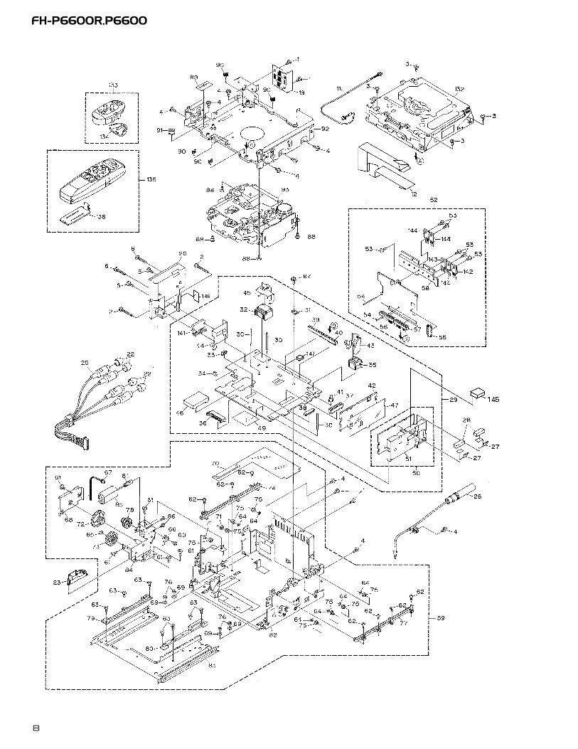
(1) EXTERIOR SECTION PARTS LIST
Mark No. Description Part No. Mark No. Description Part No.
10
FH-P6600R,P6600
91 Clamper CNV630992 Chassis Unit CXB542093 Cassette Mechanism ModuleEXK402094 Screw BPZ20P080FMC95 Panel PCB Unit See Contrast table(2)
96 Socket(CN1101) CKS355397 Connector(CN1102) CKS377098 Panel Unit CXB543799 Door CAT2150
100 Spring CBH1371
101 Screw BPZ20P080FMC102 Button(ANGLE) CAC6533103 Button(1-6,etc) CAC6534104 Button(EJECT) CAC6535105 Button(F,A) CAC6537
106 Button(SEL) CAC6538107 Lever(SOURCE) CAC6539108 IC(IC1903) SBX8035-H109 Lever(VOLUME) CAC6540110 Button(CD EJ) CAC6541
111 Button(DSP,BAND) CAC6542112 Cushion CNM6646113 Insulator CNM6647
* 114 Cushion CNM6938115 PCB CNP5309
116 Holder CNV6136117 Roller CNV6172118 Flap PCB Unit See Contrast table(2)119 LCD(LCD1901) CAW1593120 Connector(CN1901) CKS3774
121 Connector(CN1201) CKS4274122 Connector(CN1902) CKS4275123 Holder CNC8699124 Sheet CNM6642125 Spacer CNM6644
126 Insulator CNM6719127 Spacer CNM6940128 Lighting Conductor CNV6133129 Connector CNV6135130 Case Unit CXB5262
131 Grille Unit See Contrast table(2)132 CD Mechanism Module(S8TX) CXK5210133 Remote Control Assy See Contrast table(2)134 Cover See Contrast table(2)135 Remote Control Assy See Contrast table(2)
136 Battery Cover See Contrast table(2)137 Cord Assy See Contrast table(2)138 Cap See Contrast table(2)139 Resistor See Contrast table(2)140 Fuse(10A) See Contrast table(2)
141 IC(IC351) PAL005A142 IC(IC903) SBX8035-H143 IC9IC907) PQ20RX1S-L144 Transistor(Q912,Q915,Q921) 2SD2396145 Cushion CNM6870
146 Cushion CNM6997147 Spacer CNM7014
Mark No. Description Part No. Mark No. Description Part No.

11
FH-P6600R,P6600
Part No.Mark No. Symbol and Description FH-P6600R/EW FH-P6600/ES
13 Cord Assy CDE6404 Not used14 Fuse(10A) CEK1136 Not used15 Cap CKX-003 Not used16 Cap CNS1472 Not used17 Resistor RS1/2PMF102J Not used
29 Audio Amp Unit CWM7006 CWM700149 Insulator CNM6034 Not used50 FM/AM Tuner Unit CWE1500 CWE150152 Power Supply Unit CWM7007 CWM700295 Panel PCB Unit CWM7008 CWM7003
118 Flap PCB Unit CWM7009 CWM7004131 Grille Unit CXB6482 CXB6483133 Remote Control Assy CZX3218 Not used134 Cover CZN6410 Not used135 Remote Control Assy Not used CXB3877
136 Battery Cover Not used CNS5032137 Cord Assy Not used CDE6257138 Cap Not used CNS1472139 Resistor Not used RS1/2PMF102J140 Fuse(10A) Not used CEK1136
(2) CONTRAST TABLE
FH-P6600R/EW and FH-P6600/ES are constructed same except for the following:

12
FH-P6600R,P6600
2.4 CD MECHANISM MODULE

13
FH-P6600R,P6600
- CD MECHANISM MODULE SECTION PARTS LIST
1 Control Unit(S8TX) CWX24342 Connector(CN802) CKS21923 Connector(CN801) CKS21934 Connector(CN701) CKS42815 Connector(CN101) CKS3486
6 Screw BMZ20P030FMC7 Screw BSZ20P040FMC8 Screw(M2x3) CBA10779 Screw(M2x5) EBA1028
10 Screw(M2x2) CBA1523
11 Screw(M2x4) CBA136212 Washer CBF103713 Washer CBF103814 Washer CBF106015 •••••
16 Spring CBH207917 Spring CBH211718 Spring CBH231419 Spring CBH211020 Spring CBH2282
21 Spring CBH231822 •••••23 Spring CBH232424 Spring CBH211825 Spring CBH2161
26 Spring CBH216327 Spring CBH218928 Spring CBH224929 Spring CBH226030 Spring CBH2262
31 Bracket CNC856832 Spring CBL136933 Connector CDE553134 Connector CDE553235 Shaft CLA3304
36 Screw(M2.6x6) CBA145837 Frame CNC868238 Frame CNC889239 Lever CNC869440 Arm CNC8663
41 Bracket CNC856742 •••••43 Spacer CNM331544 Sheet CNM665945 •••••
46 •••••47 Ball CNR118948 Belt CNT108649 Roller CNV450950 Arm CNV6102
51 Arm CNV609452 Arm CNV524853 Arm CNV609554 Guide CNV525455 Guide CNV5255
56 Gear CNV525757 Gear CNV525658 Guide CNV617659 Damper CNV601060 Arm CNV6096
61 Arm CNV603162 Arm CNV621163 Guide CNV601264 Guide CNV551065 •••••
66 Guide CNV575167 Clamper CNV601368 Gear CNV581369 Motor Unit(M1) CXB582770 Screw Unit CXB4726
71 Chassis Unit CXB581172 Gear Unit CXB4728
* 73 Arm Unit CXB575374 Motor Unit(M2) CXB582875 Lever Unit CXB6049
76 Arm Unit CXB473177 Motor Unit(M3) CXB582978 Arm Unit CXB568979 Bracket Unit CXB479580 Screw JFZ20P025FMC
81 Screw JGZ17P025FZK82 Washer YE20FUC83 Pickup Unit(Service)(P8) CXX128584 Screw IMS26P030FMC
* 85 Gathering PCB CNX2982
86 Photo Transistor(Q1, 2) CPT230SX-TU87 Damper CNV601188 Rack CNV601489 Spring CBH231590 Connector(CN601) CKS4282
91 Connector(CN602) CKS2191
Mark No. Description Part No. Mark No. Description Part No.

14
FH-P6600R,P6600
2.5 CASSETTE MECHANISM MODULE

15
FH-P6600R,P6600
- CASSETTE MECHANISM MODULE SECTION PARTS LIST
1 Screw BSZ20P040FMC2 Washer CBF10373 Washer CBG10034 Screw EBA10285 Screw CBA1037
6 Spring EBH15317 Spring EBH16248 Spring EBH16259 Spring EBH1626
10 Spring EBH1627
11 Spring EBH162912 Cord EDD102413 Photo-reflector(EGN1) EGN100414 Arm ENC152615 Lever ENC1530
16 Lever ENC153117 Arm ENC153218 Frame ENC153319 Holder ENC153420 Gear ENC1535
21 Arm ENC153622 Roller ENR104023 Belt ENT102724 Collar ENV150825 Arm ENV1539
26 Arm ENV154027 Gear ENV154428 Gear ENV154729 Gear ENV154830 Worm Wheel ENV1550
31 Lever ENV155132 Flywheel ENV155433 Gathering PCB ENX105434 Switch(S1,S2,S3) ESG100735 Deck Unit EWM1029
36 Plug(CN251) CKS354037 PCB ENP118438 Motor Unit(M1) EXA149039 Motor EXM102740 Head Assy(HD1) EXA1589
41 Motor Unit(M2) EXA158042 Screw BMZ20P022FMC43 Bracket ENC152844 Chassis Unit EXA158245 Pinch Holder Unit EXA1584
46 Pinch Roller ENV151847 Pinch Holder Unit EXA158348 Pinch Roller ENV151849 Reel Unit EXA158550 Head Base Unit EXA1586
51 Lever Unit EXA158752 Gear Unit EXA158853 Motor Unit(Service) EXX105554 Washer HBF-17955 Screw CBA1250
56 Bracket ENC154257 Arm ENC1537
Mark No. Description Part No. Mark No. Description Part No.
16
A
1 2 3 4
B
C
1 2 3 4
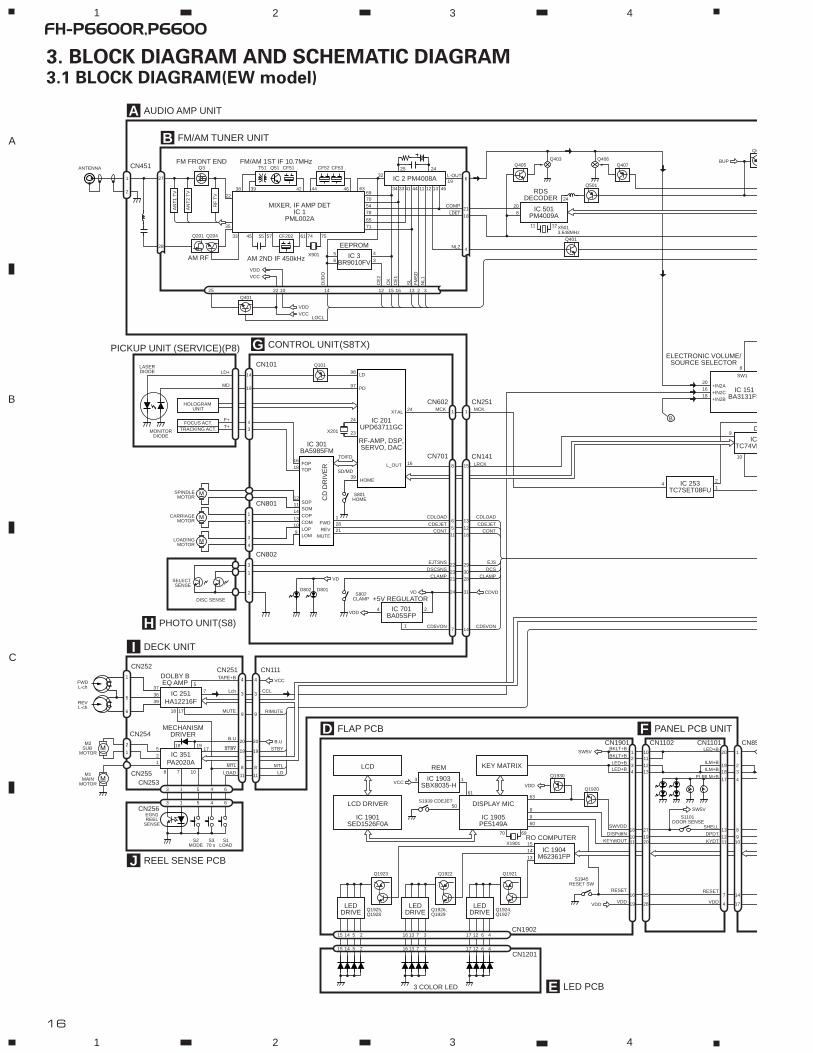
3. BLOCK DIAGRAM AND SCHEMATIC DIAGRAM3.1 BLOCK DIAGRAM(EW model)
FH-P6600R,P6600
B FM/AM TUNER UNIT
A AUDIO AMP UNIT
CN451
RDSDECODER
CDVD
CDLOAD
CDEJETCONT
EJTSNS
DSCSNS
CLAMP
CD5VON
CDLOAD
CDEJETCONT
EJS
DCS
CLAMP
CD5VON
G CONTROL UNIT(S8TX)
H PHOTO UNIT(S8)
Q401
X5013.648MHz
Q405
Q501
Q407Q403 Q406
8
11 12
20
24
8
10
9
2
1
+IN2A
SW120
4
+IN2C16
+IN2B18
4
18
21
6
NL2
ldet
COMP
L-OUT
IC 501PM4009A
Q3
CF202
X901
VDDVCC
LOCL
VDDVCC
ANTENNA
27
28
1
2
Q201 Q204
T51 Q51 CF51 CF52 CF53A
NT
1 T
V
AN
T2
TV
RF
TV
AM RF
EEPROM
IC 3BR9010FV
MIXER, IF AMP DETIC 1
PML002A
FM/AM 1ST IF 10.7MHz
AM 2ND IF 450kHz
FM FRONT END
56
4
3
35
33
38 42 46
32
4439
45 55 57 61 74 75
7165
78547069
63
25 24
19
46131211444134 33
22
IC 2 PM4008A
22 10 14 12 15 16 13 2 3
DI/D
O
CE
2
CK
CE
1
SL
FM
SD
NL1
IC 151BA3131FS
ELECTRONIC VOLUME/SOURCE SELECTOR
Q401
25
Q4
BUP
B
SELECTSENSE
DISC SENSE
D802 D801S802
CLAMP
LD
L_OUT
PD
HOME
RF-AMP, DSP,SERVO, DAC
IC 201UPD63711GC
IC 301BA5985FM
12
1618
1114
13109
SOP
TOPFOP
SOM
COPCOMLOPLOM
FWDREV
MUTE
CD
DR
IVE
R
XTAL
LASERDIODE
MONITORDIODE
FOCUS ACT.TRACKING ACT.
LD+
MD
F+
T+
14
19
4
3
PICKUP UNIT (SERVICE)(P8)
HOLOGRAM UNIT
Q101
M
M
M
SPINDLEMOTOR
CARRIAGEMOTOR
LOADINGMOTOR
TD/FD
SD/MD
24
97
MCK MCK
LRCK
98
24
12821
16
23
39
X201
CN701
CN602 CN251
CN141
1
8
22
23
21
24
7
6
5
11
1
15
29
30
28
31
14
13
12
18
S801HOME
CN101
1
2
3
4
CN801
3
1
2
CN802
VD
IC 701BA05SFP
4 2
1
VD
VDD
ICTC74VH
IC 253TC7SET08FU
M
M
CN252
CN254
CN255
CN256
CN253
CN251 CN111DOLBY BEQ AMP
MECHANISMDRIVER
1
64513
64513
5
6
2
1
S370 s
S1LOAD
S2MODE
EGN1REEL
SENSE
M1MAIN
MOTOR
M2SUB
MOTOR
REVL-ch
FWDL-ch
8 7 10
12
5
TAPE+BVCC
B.U
Lch CCL
MUTE
B.U
stby
mtl
LOAD
MTL
LD
STBY
RIMUTE1718
3936
37
171918
75
IC 251HA12216F
IC 351PA2020A
J REEL SENSE PCB
I DECK UNIT
S1101 DOOR SENSE
S1945RESET SW
1
23
4
8
910
14
20
1918
17
13
1211
7
174
11ILM+B
LED+BBKLT+B
BKLT+B
LED+BLED+B
SWVDD
DISPdtIN
KEYdtOUT
RESET
VDD
ILM+B
FLPILM+B
SHELL
DPDT
KYDT
RESET
VDD
SW5V
KEY MATRIXQ1930
Q1920
SW5V
IC 1904M62361FP
DISPLAY MIC
IC 1905PE5149A
LCD DRIVER
IC 1901SED1526F0A
LCD
RO COMPUTER
3 COLOR LED
LEDDRIVE
Q1923
Q1925,Q1928
LEDDRIVE
Q1922
Q1926,Q1929
LEDDRIVE
Q1921
Q1924,Q1927
+5V REGULATOR
4
3
9
20
19
8
11
4
3
9
20
19
8
11
CN1101 CN85CN1901 CN1102
CN1902
CN1201
VDD
10
1213
27
1920
25
28
21
34
18
1011
16
19
15 14 5 2 16 13 7 3 17 12 6 4
15 14 5 2 16 13 7 3 17 12 6 4
50
3 1
6163
1514
13
8
960
VDD
S1939 CDEJET
X1901
70 69
IC 1903SBX8035-H
REM
VCC
D FLAP PCB
E LED PCB
F PANEL PCB UNIT
D

17
FH-P6600R,P66005 6 7 8
5 6 7 8
A
B
C
D
BUP
8
10 4
9
9
FLAP1
CDVD
BUP
85FLAP0
84
FLAPPW86
bsens96
asens97
VDSENS112
FLIN
RLIN
SYSPW
12
14
22 4 25
OUT214
8
RL—23
RL+21
FL—3
FL+
RL—
ACC
GND
BUPBUP
BUP
RL+
FL—
BREM
FL+
FL
SUBL
5
2A
SW1 SW2
13 362C2B
SL106
NL1107
126TUNPCE
129TUNPCK
125
TUNPDO127
TUNPDILOCL5
SOR029
SOR130
TUNPCE2128
SD2
NL2DT23
ldet101
FM/am7
tmute8
IC 151BA3131FS
IC 351PAL005A
LUME/CTOR
POWER AMP
SLIDE POSITION SENSESYSTEMMICRO COMPUTER
IC 601 (1/2)PE5124A
MUTE STBY B.REM
Q871
Q802
Q408
Q803
Q801
Q931
Q932
2
1
5
91110
12
4
ILL
RL—
ACC
GND
BUP
RL+
FL—
BREM
FL+
ILL3
TELMUTE8
CN853
A
BUP IC 805BA6288FS
11
6
14
135 4
MT2MT1
12
CN801
MOTORUNIT
X210
X111
X6016.291456MHz
SWVDD137
FLSEN1116
FLSEN0115
IC 801TC7W14FU
7
5
2
4
IC 804GP1S94J
1 2
IC 803GP1S94J
1 2
SW5V
VDD
IC 153NJM4558MD LIN
58BFOT
76LRCK
DSP
IC 251PDG255A
IC 303NJM4558MD
5 7
IC 304NJM4558MD
3 1
5 7
6 19
7 18
8 17
AOUTL239
AOUTL352
AOUTL127
IC 301PM0017AM
IC 252TC74VHC125FT
MCK_OUT42
DSPMS131
RIMUTE
LOADSW
MTLSWSTBY
76
757071
ILMPW77
SHEEL94
DPDT138
KEYDT139
RESET9
flapejsw114
fopnsw82
fclssw83
Q251
S801 FEJSWS802 FOPNSWS803 FCLSSW
Q854
Q853
Q351XTALI38
42XTALO38
41 X25116.9344MHz
BUP
Q852A
Q352
Q937
1
1
CN857
1
56
2
CN901CN903
CN903 CN857
Q938Q927
Q935
Q936
BUPQ916
Q917
Q915
BUP
Q932
Q931
Q851
Q913
Q914
Q912
Q933BZ901ALARMBUZZER
BUP
Q926
Q925
32 IC 902S-81250SGUP
3
2
1 IC 907PQ20RX1S-L
31 IC 903BA033T
IC 904CA0008AM
1
2
6
55
IC 905TA2050F
112
14
BUPQ922
Q923
Q921
81
5
7
11
CN131
CDVD
A8V
TUNVDD
LED+8
A3V
BUSL2BUSL1
BUS—BUS+
ASENB
ILL
VDD
CDLOAD
CONTSDEJECT
59
5855
EJTSNS
CLAMPDSCSNS
110
11154
CD5VON25
Q872
Q874
Q875
FLAPILM36
BUP
1
23
4
8
910
14
20
1918
17
13
1211
7
174
LED+B
IC 602S-80734ANDYI
2 1
VDD
MUTE
FL
SWL
MUTE
TELIN
ISENS
ASENBO
VDCNTCD
MUTE
SYSPW
PEE
BKLT
TX
RX
IPPW
IPL
DALMON
79
TEL_IN117
isens98
ASENBO87
VDCONT56
SYSPW80
PEE144
BKLT26
TX89
RX90
IPPW88
DALMON81
16
15
27
23
30
29
6
16
15
27
23
30
29
6
28 28
CN902 CN85630 30
28 28
13 13
10 10
17 17
14 14
11 11
CN903 CN857
13
9 924 24
14 14
13
CN856 CN90218 18
CN857 CN9032 2
3 3
7 7
8 8
25 25
10 10
12 12
5 5
B
SYSTEMMICRO COMPUTER
IC 601 (2/2)PE5124A
RESET
CN854
NIT
C POWER SUPPLY UNIT
TELMUTE
ILL
ASEN(IP)
CD+B
SYS+B
TU5V
LED+B
DSP+B
BUS+
BUS—
L+L—
DSP
MIX
E VOL
CDREG.
SYS REG.
TUNVDD REG.
LED REG.
DSP REG.
IP-DRIVER
IP ISOLATOR
RC
A
IP-BUS
FL+
RL+
RR+
RL+
FL—
RL—
RR—
RL—ACC
ANT
GND
ILL
BACKUP

18
FH-P6600R,P6600
A
1 2 3 4
B
C
D
1 2 3 4
CN701 CN602CONTROL UNIT
FM/A
M T
UN
ER
UN
ITI
CN251
ANTENNA
MOTORUNIT
G
B
FM(100%)EW :-15.5dBsFM(100%)ES :-19.5dBsAM(30%)EW :-26dBsAM(30%)ES :-30dBsIP-BUS :+1.2dBsTAPE :-12.8dBs
TAPE :-9dBs
FM(1
00%
)EW
:-15
.5d
Bs
FM(1
00%
)ES
:-19
.5d
Bs
AM
(30%
)EW
:-26
dB
sA
M(3
0%)E
S:-
30d
Bs
A
A-aA-a A-b A-b
A-aA-a A-b A-b
A-b A-b A-a A-a
Large sizeSCH diagram
Guide page
Detailed page
A-a3.2 OVERALL CONNECTION DIAGRAM(GUIDE PAGE)
Note: When ordering service parts, be sure to refer to “EXPLODED VIEWS AND PARTS LIST” or “ELECTRICAL
PARTS LIST”.
FH-P6600R,P66005 6 7 8
A
B
C
D
5 6 7 8
19
CN1101
Decimal points for resistorand capacitor fixed valuesare expressed as :2.2 2R20.022 R022
← ←
The > mark found on some component parts indicatesthe importance of the safety factor of the part.Therefore, when replacing, be sure to use parts ofidentical designation.
Symbol indicates a resistor.No differentiation is made between chip resistors anddiscrete resistors.
NOTE :
Symbol indicates a capacitor.No differentiation is made between chip capacitors anddiscrete capacitors.
>
>
>
PANEL PCB UNIT
CCN902
CCN903
IP-B
US
F
AUDIO AMP UNITA
FL+
RL+
RR+
RL+
FL—
RL—
RR—
RL—ACC
ANT
GND
ILL
BACKUP
EW
dBsdBsssBs
dBsFM(100%)EW :-0.8dBsFM(100%)ES :-4.8dBsAM(30%)EW :-11.3dBsAM(30%)ES :-15.3dBsIP-BUS :+1.2dBsTAPE :-12.8dBs
FM(100%)EW :-6.8dBsFM(100%)ES :-10.8dBsAM(30%)EW :-17.3dBsAM(30%)ES :-21.3dBsIP-BUS :-4.8dBsTAPE :-18.8dBs
FM(100%)EW :-4.4dBsFM(100%)ES :-8.4dBsAM(30%)EW :-14.9dBsAM(30%)ES :-18.9dBsIP-BUS :-2.4dBsCD :-1.4dBsTAPE :-16.4dBs
FM(100%)EW :+3.2dBsFM(100%)ES :-0.8dBsAM(30%)EW :-7.3dBsAM(30%)ES :-11.3dBsIP-BUS :+5.2dBsCD :+6.2dBsTAPE :-8.8dBs
FM(100%)EW :+8.2dBsFM(100%)ES :+4.2dBsAM(30%)EW :-2.3dBsAM(30%)ES :-6.3dBsIP-BUS :+10.2dBsCD :+11.2dBsTAPE :-3.8dBs
FM(100%)EW :+34.2dBsFM(100%)ES :+30.2dBsAM(30%)EW :+23.7dBsAM(30%)ES :+19.7dBsIP-BUS :+36.2dBsCD :+37.2dBsTAPE :+22.2dBs
IP-B
US
:+2.
2dB
s
A
A-b

20
FH-P6600R,P6600
CN
701
CN
602
CO
NT
RO
L U
NIT
UNIT
IC
N25
1
G
FM(1
00%
)EW
:-15
.5d
Bs
FM(1
00%
)ES
:-19
.5d
Bs
AM
(30%
)EW
:-26
dB
sA
M(3
0%)E
S:-
30d
Bs
IP-B
US
:+1.
2dB
sTA
PE
:-12
.8d
Bs
TAP
E :-
9dB
s
FM(100%)EW:-15.5dBsFM(100%)ES:-19.5dBsAM(30%)EW:-26dBsAM(30%)ES:-30dBs
A
1 2 3 4
B
C
D
1 2 3 4
A-a
A-b
A-a
1 2 3 4
21
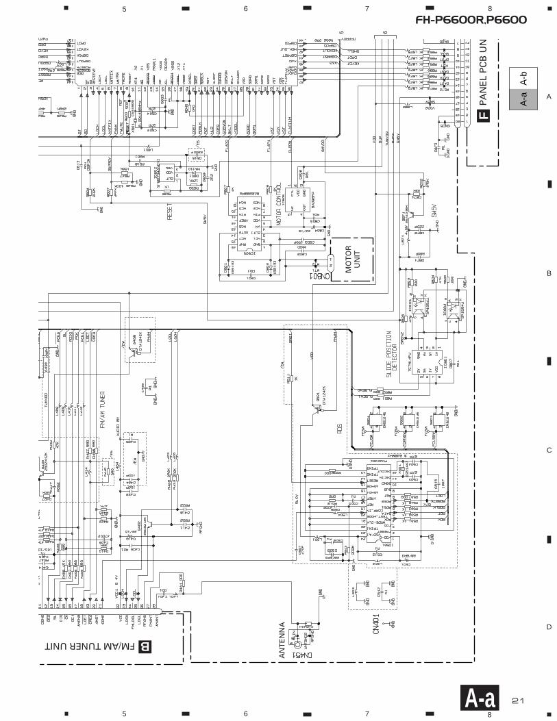
FH-P6600R,P6600
FM/AM TUNER UNIT
PA
NE
L P
CB
UN
AN
TE
NN
A
MO
TO
RU
NIT
F
B
5 6 7 8
A
B
C
D
5 6 7 8
A-a
A-b
A-a
5 6

22
FH-P6600R,P6600
AU
DIO
AM
P U
NIT
A
RR
RR
EW
FM(1
00%
)EW
:-0.
8dB
sFM
(100
%)E
S:-
4.8d
Bs
AM
(30%
)EW
:-11
.3d
Bs
AM
(30%
)ES
:-15
.3d
Bs
IP-B
US
:+1.
2dB
sTA
PE
:-12
.8d
Bs
FM(1
00%
)EW
:-6.
8dB
sFM
(100
%)E
S:-
10.8
dB
sA
M(3
0%)E
W:-
17.3
dB
sA
M(3
0%)E
S:-
21.3
dB
sIP
-BU
S:-
4.8d
Bs
TAP
E:-
18.8
dB
s
FM(1
00%
)EW
:-4.
4dB
sFM
(100
%)E
S:-
8.4d
Bs
AM
(30%
)EW
:-14
.9d
Bs
AM
(30%
)ES
:-18
.9d
Bs
IP-B
US
:-2.
4dB
sC
D:-
1.4d
Bs
TAP
E:-
16.4
dB
s
FM(1
00%
)EW
:+3.
2dB
sFM
(100
%)E
S:-
0.8d
Bs
AM
(30%
)EW
:-7.
3dB
sA
M(3
0%)E
S:-
11.3
dB
sIP
-BU
S:+
5.2d
Bs
CD
:+6.
2dB
sTA
PE
:-8.
8dB
s
FM(1
00%
)EW
:+8.
2dB
sFM
(100
%)E
S:+
4.2d
Bs
AM
(30%
)EW
:-2.
3dB
sA
M(3
0%)E
S:-
6.3d
Bs
IP-B
US
:+10
.2d
Bs
CD
:+11
.2d
Bs
TAP
E:-
3.8d
Bs
FM(1
00%
)EW
:+34
.2d
Bs
FM(1
00%
)ES
:+30
.2d
Bs
AM
(30%
)EW
:+23
.7d
Bs
AM
(30%
)ES
:+19
.7d
Bs
IP-B
US
:+36
.2d
Bs
CD
:+37
.2d
Bs
TAP
E:+
22.2
dB
s
A
1 2 3 4
B
C
D
1 2 3 4
A-a
A-b
A-b
1 2 3 4

23
FH-P6600R,P6600
CN
1101
Dec
imal
po
ints
fo
r re
sist
or
and
cap
acit
or
fixe
d v
alu
esar
e ex
pre
ssed
as
:2.
2
2R2
0.02
2
R02
2
←
←
Th
e >
mar
k fo
un
d o
n s
om
e co
mp
on
ent
par
ts in
dic
ates
the
imp
ort
ance
of
the
safe
ty f
acto
r o
f th
e p
art.
Th
eref
ore
, wh
en r
epla
cin
g, b
e su
re t
o u
se p
arts
of
iden
tica
l des
ign
atio
n.
Sym
bo
l in
dic
ates
a r
esis
tor.
No
dif
fere
nti
atio
n is
mad
e b
etw
een
ch
ip r
esis
tors
an
dd
iscr
ete
resi
sto
rs.
NO
TE
:
Sym
bo
l in
dic
ates
a c
apac
ito
r.N
o d
iffe
ren
tiat
ion
is m
ade
bet
wee
n c
hip
cap
acit
ors
an
dd
iscr
ete
cap
acit
ors
.
>
>
>
CB
UN
IT
C CN
902
C CN
903
IP-BUS
FL +RL +RR + RL +
FL —RL —RR — RL —
AC
C
AN
T
GN
D
ILL
BACK UP
EW
IP-BUS :+2.2dBs
5 6 7 8
A
B
C
D
5 6 7 8
A-a
A-b
A-b
5 6

24
FH-P6600R,P6600
A
1 2 3 4
B
C
D
1 2 3 4
B
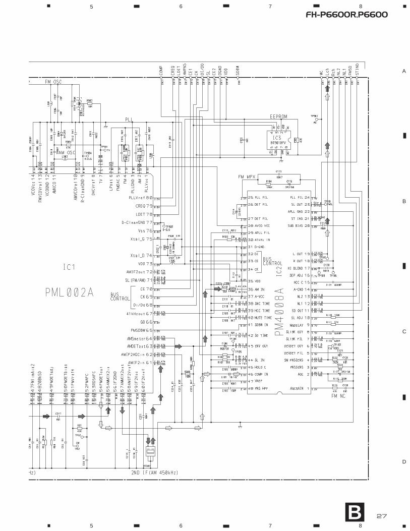
3.3 FM/AM TUNER UNIT(FH-P6600R/EW)
KV
1410
(23)
KV
1410
(23)
MarkNoneF0F65F125A0A74A125
Band–FMFMFMAMAMAM
Input Level–0dBf65dBf125dBf0dBµ74dBµ125dBµ
DA
N21
7U
DA
N21
7U
BA
FM/AM TUNER UNIT

25
FH-P6600R,P66005 6 7 8
A
B
C
D
5 6 7 8B
KV
1410
(23)

26
FH-P6600R,P6600
A
1 2 3 4
B
C
D
1 2 3 4
B
3.4 FM/AM TUNER UNIT(FH-P6600/ES)
KV
1410
(23)
MarkNoneF0F65F125A0A74A125
Band–FMFMFMAMAMAM
Input Level–0dBf65dBf125dBf0dBµ74dBµ125dBµ
DA
N21
7U
BA
FM/AM TUNER UNIT
27
FH-P6600R,P66005 6 7 8
A
B
C
D
5 6 7 8
B
KV
1410
(23)
28
FH-P6600R,P6600
AC
N85
7
AC
N85
6
A
1 2 3 4
B
C
D
1 2 3 4
C
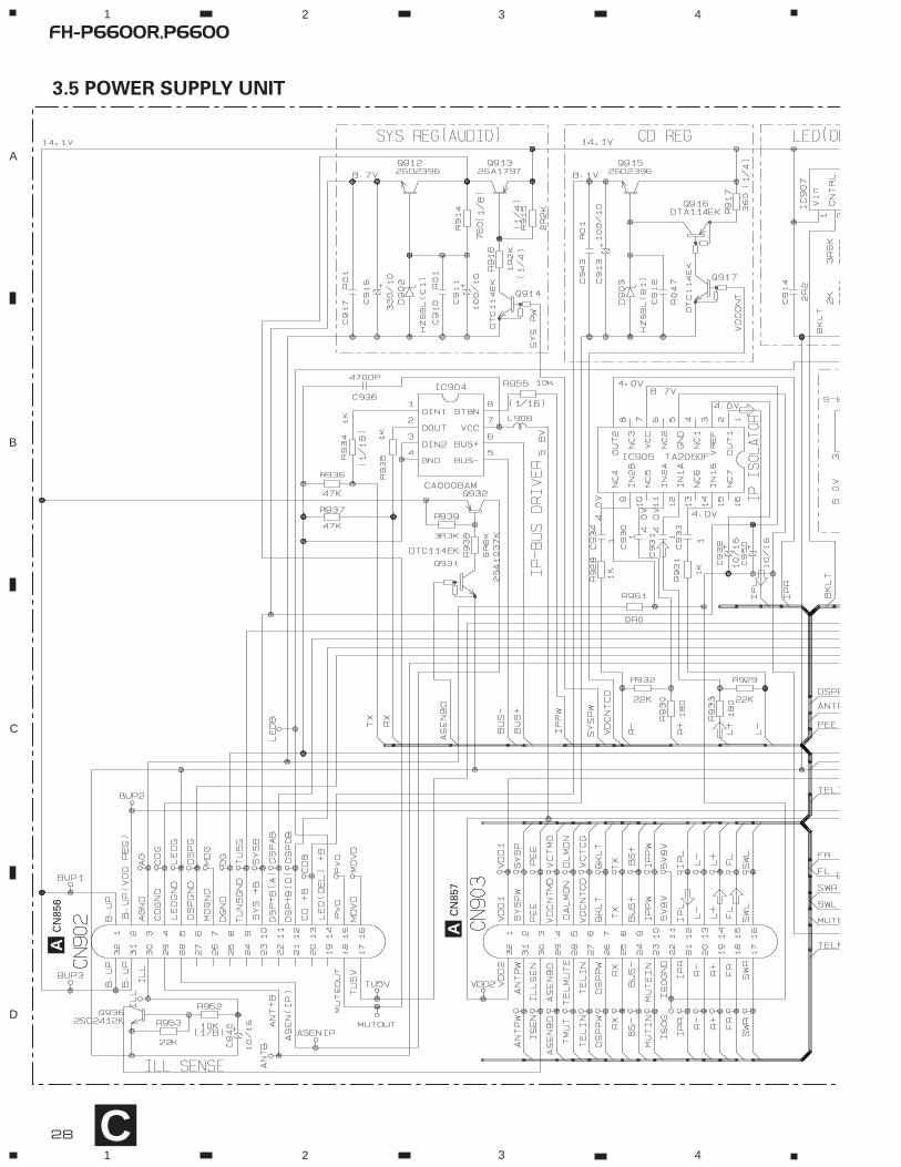
3.5 POWER SUPPLY UNIT

29
FH-P6600R,P6600
/ES
RC
A C
OR
D
C POWER SUPPLY UNIT
5 6 7 8
A
B
C
D
5 6 7 8C

30
FH-P6600R,P6600
PTY
D.FUNC
TAPE
CN1102
CN1201
F
EA
1 2 3 4
B
C
D
1 2 3 4D
3.6 FLAP PCB

31
FH-P6600R,P66005 6 7 8
A
B
C
D
5 6 7 8D
F
D FLAP PCB UNIT
FLAP PCB UNITConsists ofFLAP PCBLED PCB

32
FH-P6600R,P6600
D
E
CN
1902
FLA
P P
CB
UN
ITC
on
sist
s o
fFL
AP
PC
BLE
D P
CB
LED
PC
B
A
1 2 3 4
B
C
D
1 2 3 4
3.7 LED PCB
E

33
FH-P6600R,P66001 2 3 4
A
B
C
D
1 2 3 4
F
ACN854
DCN1901
PANEL PCB UNIT
F
3.8 PANEL PCB UNIT

34
FH-P6600R,P6600
A
1 2 3 4
B
C
D
1 2 3 4
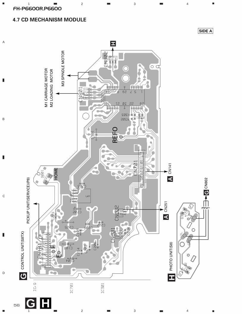
3.9 CD MECHANISM MODULE
H
G H
SPINDLE MOTOR
Q2 CPT230SX-TUQ1 CPT230SX-TU
M3 CXB5829
CARRIAGE MOTOR
M1 CXB5827
M2 CXB5828
LOADING MOTOR
CN101
CN802
CN801
RF-AM
CD DRIVER
5V REGULATOR
CONTROL UNIT(S8TX)
PHOTO UNIT(S8)
G
PICKUP UNIT(SERVICE)(P8)

SWITCHES:CONTROL UNIT S801 : HOME SWITCH.....ON-OFF S802 : CLAMP SWITCH....ON-OFFThe underlined indicates the switch position.
CN601
CN602
CN701
RF-AMP, SERVO, DSP, DAC, LPF
35
FH-P6600R,P66005 6 7 8
A
B
C
D
5 6 7 8
AC
N14
1
G
A CN251

36
FH-P6600R,P6600
1 RFI 0.5V/div. 0.5µs/div.Normal mode: play
1 CH1: RFI 1V/div.2 CH2: MIRR 5V/div.
Test mode: Tracking open
0.5ms/div. 1 CH1: RFI 1V/div.2 CH2: MIRR 5V/div.
Normal mode: The defect partpasses 800µm
0.5ms/div.
3 CH1: FD 0.5V/div.4 CH2: FO+ 2V/div.
Test mode: No disc, Focus close
0.2s/div. 3 CH1: FD 0.5V/div.5 CH2: FOK 2V/div.
Normal mode: Focus close
0.2s/div. 6 CH1: FE 0.5V/div.7 CH2: XSI 2V/div.
Normal mode: Focus close
1ms/div.
REFO →
8 CH1: TE 0.5V/div.9 CH2: TD 0.5V/div.
Test mode: 32 tracks jump (FWD)
0.5ms/div. 8 CH1: TE 0.5V/div.9 CH2: TD 0.5V/div.
Test mode: Single jump (FWD)
0.5ms/div. 8 CH1: TE 0.5V/div.9 CH2: TD 0.5V/div.
Test mode: 100 tracks jump (FWD)
5ms/div.
6 CH1: FE 0.1V/div.3 CH2: FD 0.2V/div.
Normal mode: Play
20ms/div. 3 CH1: FD 0.5V/div.0 CH2: MD 1V/div.
Normal mode: Focus close (12cm)
0.5s/div. 3 CH1: FD 0.5V/div.0 CH2: MD 1V/div.
Normal mode: Focus close (8cm)
0.5s/div.
REFO →
REFO →
REFO →
REFO →
REFO →
REFO →
GND →
REFO →
REFO →
REFO →
REFO →
REFO →
REFO →
REFO →
REFO →
REFO →
REFO →
REFO →
REFO →
- Waveforms
Note:1. The encircled numbers denote measuring pointes in the circuit diagram.2. Reference voltage
REFO:2.5V
REFO →
REFO →
REFO →
REFO →

37
FH-P6600R,P6600
8 CH1: TE 0.2V/div.9 CH2: TD 0.2V/div.
Normal mode: play
8 CH1: TE 0.5V/div.! CH2: SD 0.5V/div.TEST mode: 100 Tracks jump(FWD)
5ms/div. 0 MD 0.5V/div. 0.1s/div.
Normal mode: Play (12cm)
0 MD 1V/div. 10ms/div.Normal mode:Long Search (12cm)
@ EFM 1V/div. 5µs/div.
Normal mode: play
8 CH1: TE 1V/div.# CH2: TEC 1V/div.
Test mode: Focus closeTracking open
2ms/div.
8 CH1: TE 0.5V/div.6 CH2: FE 0.5V/div.
Normal mode: AGC after focus close
0.2s/div.$ PLCK 2V/div. 0.5µs/div.
Normal mode: play
20ms/div.
% SCKO 2V/div. 1µs/div.
Normal mode: play
^ Dout 2V/div. 10µs/div.
Normal mode: play
& LRCK 2V/div. 20µs/div.
Normal mode: play
* VD 5V/div. 50ms/div.
Normal mode: No disc
GND →
REFO →
REFO →
GND →
REFO →
REFO →
REFO →
REFO →REFO →
REFO →
REFO →
REFO →
REFO →
GND →
REFO →
GND →
REFO →
GND →
REFO →
GND →
REFO →

38
FH-P6600R,P6600
6 CH1: FE 0.2V/div.3 CH2: FD 0.5V/div.
Normal mode: During AGC
1ms/div. 8 CH1: TE 0.2V/div.9 CH2: TD 0.5V/div.
Normal mode: During AGC
1 CH1: RFI 1V/div.⁄ CH2: HOLD 5V/div.
Normal mode: The defect part passes800µm(B.D)
1ms/div. 0.5ms/div.
3 CH1: FD 0.5V/div.⁄ CH2: HOLD 5V/div.
Normal mode: The defect part passes800µm(B.D)
0.5ms/div.9 CH1: TD 0.1V/div.⁄ CH2: HOLD 5V/div.
Normal mode: The defect part passes800µm(B.D)
0.5ms/div.
REFO →
REFO →
REFO →
REFO →
REFO →
REFO →
REFO →
REFO →
REFO →
REFO →

39
FH-P6600R,P6600

40
FH-P6600R,P6600
A
1 2 3 4
B
C
D
1 2 3 4
3.10 CASSETTE MECHANISM MODULE
I
CN111A
DECK UNIT
MU
TE
HA12216F
11121314151617181920
40393837363534333231
30 29 28 27 26 25 24 23 22 21
1 2 3 4 5 6 7 8 9 10
R256
180
R291
0R0
C271
1/50
R283 0R0
R284 0R0
R282 0R0
C253 390P
C254 390P
C252 390P
C251 330P
R281 0R0
R255
180P
C25
6
R01
R258
18K
R40
2
3R3K
R403 910
R32
2
0R0
R293
0R0
C272 R1
R28
7
0R0
R28
50R
0
HD1HEAD ASSYEXA1589
TEST TAPENCT-150(400Hz, 200nWb/m)
RL
RR
FR
FL
C30
2
R1
VR302
33K(B)
-8.24dBs(300mV)±1dB
Fwd-R
Fwd-L
Rev-R
Rev-L
NFI(L)
RIN(L)
RIP
FIN(L)
GND
GND
FIN(R)
VREF
RIN(R)
NFI(R)
M-O
UT
(R)
EQ
OU
T(R
)
TA
I(R
)
BIA
S
RA
I(R
)
PB
OU
T(R
)
DE
T(L
)
MU
TE
MSGV(R)
MAOUT
MSI
MSDET
MSGV
F/R
120/70
NR
MO
UT
(L)
EQ
OU
T(L
)
TA
I(L) NC
RA
I(L)
PB
OU
T(L
)
NC
DE
T(L
)
MS
GV
(S)
CN252
CN251
DOLBY B NR
IC251
VR301
33K(B)
C31
0
R1
C30
9
R1
R32
1
0R0
VCC
CCP1280
CCP1280
NC
MSOUT
NC
NC
R260
13K
R26
2
270K
C40
1
3900
P
R40
1
15K
R27
6
100K
C40
2
R33
C404 R01
C40
3
R02
2R
288
0R0
R27
4
0R0
R28
9
0R0
R273
0R0
R27
2
0R0
C40
Q2712SC4116
R292
0R0
R27
1
18K
C30
1
R1
R294
0R0
R259
13K
C25
5
R01
R257
18K
R26
1
270K
I

41
FH-P6600R,P66005 6 7 8
A
B
C
D
5 6 7 8JI
REEL SENSEPCB
SWITCHES:REEL SENSE PCB S1:LOAD SWITCH..........EJECT-PLAY S2:MODE SWITCH............ON-OFF S3:70µs SWITCH...............ON-OFFThe underlined indicates the switch position.
R275
47K
R35
11K
R35
21K
R35
31K
R35
41K
R373 0R0
R35
5
270K
C35
2
3900
P
R36
230
0
C35
1R
22
C35
3R
01
C35
4R
01
R374 0R0
C356 R01
C355 R1D35
21S
S35
5
M1 MOTOR UNIT(MAIN MOTOR)EXA1490
S1LOAD
ESG1007x3
S2MODE
REEL SENSE
EGN1EGN1004
M2MOTOR UNIT(SUB MOTOR)EXA1580
RS3
RS2
RS1
SC2
SC1
TAB
MC
CE
VCC2
NC
VCC
MCS
RRS
FRS
RSB
C
TAB
MS2
NC
NC
MM
SM1
RSB
GND
RS
mtl
MCS
load
CN255CN253
CN256
CN254
MECHANISMDRIVER
IC35
1
PA
2020
A
R375 0R0
S370µs
R404
270K
C405 R033
R277
220K
R27
810
0K
Q2712SC4116
J

42
FH-P6600R,P6600
E
E
E
EE
E
MOTOR UNIT
GCN602
CCORD CN902A
1 2 3 4
B
C
D
1 2 3 4A
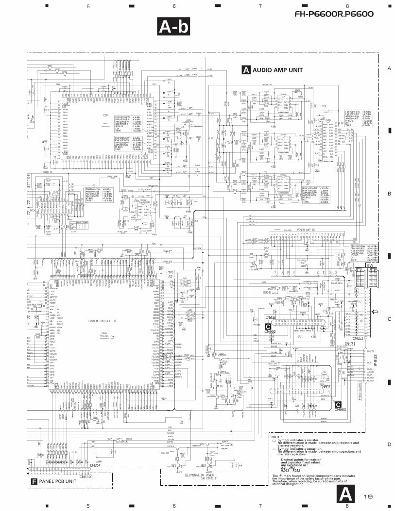
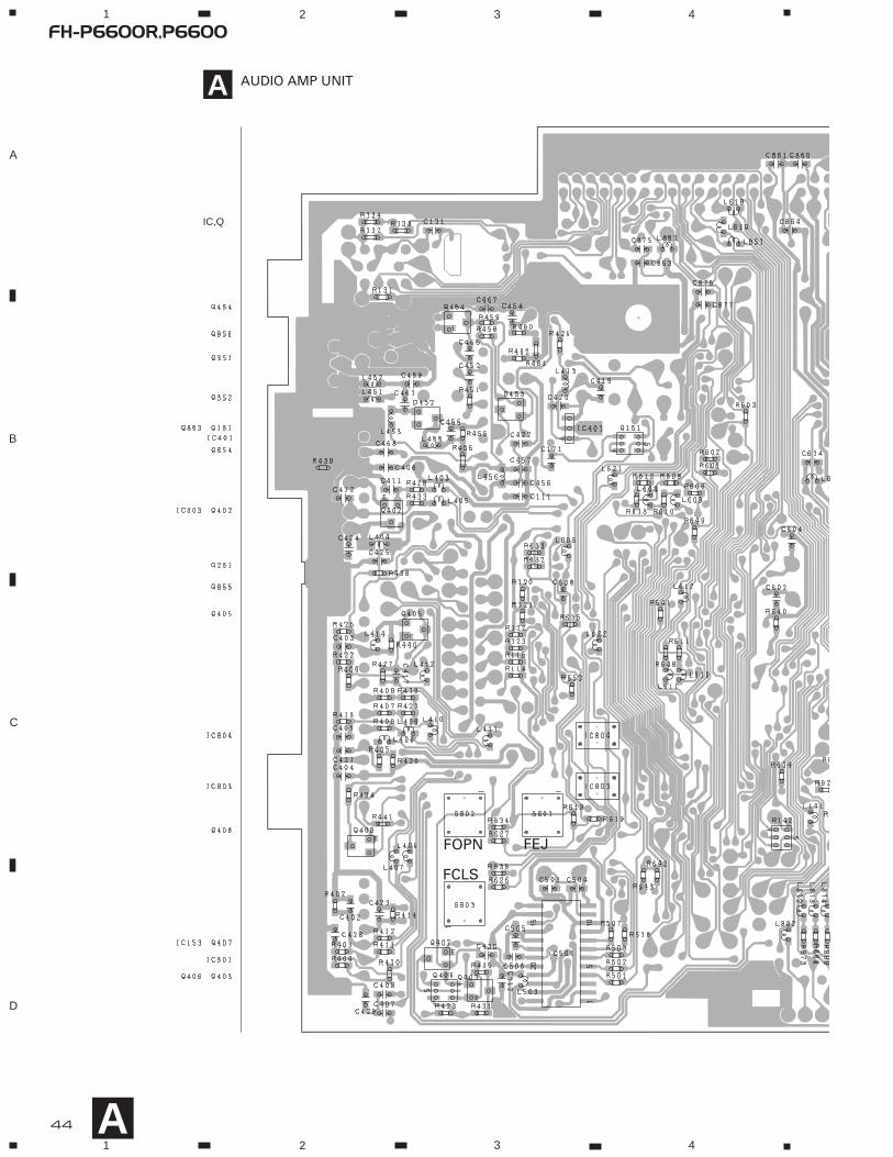
A AUDIO AMP UNIT4. PCB CONNECTION DIAGRAM
4.1 AUDIO AMP UNIT
CapacitorConnector
P.C.Board Chip Part
SIDE A
SIDE B
NOTE FOR PCB DIAGRAMS
1. The parts mounted on this PCB
include all necessary parts for
several destination.
For further information for
respective destinations, be sure
to check with the schematic
diagram.
2. Viewpoint of PCB diagrams

43
FH-P6600R,P6600
E
E
E
E
E
E
E
B
ICN251
F CN1101 G CN701
C CN903
IP-BUS
ANTENNA
IC,Q
5 6 7 8
A
B
C
D
5 6 7 8A
SIDE A
FRONT
44
FH-P6600R,P6600
E
E
E
E
E
E
IC,Q
FOPN FEJ
FCLS
A
1 2 3 4
B
C
D
1 2 3 4A
A AUDIO AMP UNIT

45
FH-P6600R,P6600
E
E
E
E
E
E
E
5 6 7 8
A
B
C
D
5 6 7 8
A
SIDE B

46
FH-P6600R,P6600
A
1 2 3 4
B
C
D
1 2 3 4
4.2 FM/AM TUNER UNIT
B
SIDE A
BFM
/AM
TU
NE
R U
NIT
A

47
FH-P6600R,P66001 2 3 4
A
B
C
D
1 2 3 4
BFM
/AM
TU
NE
R U
NIT
B
SIDE B
48
FH-P6600R,P6600
E E
E
E
E
E
E
E
CN856A
A
1 2 3 4
B
C
D
1 2 3 4
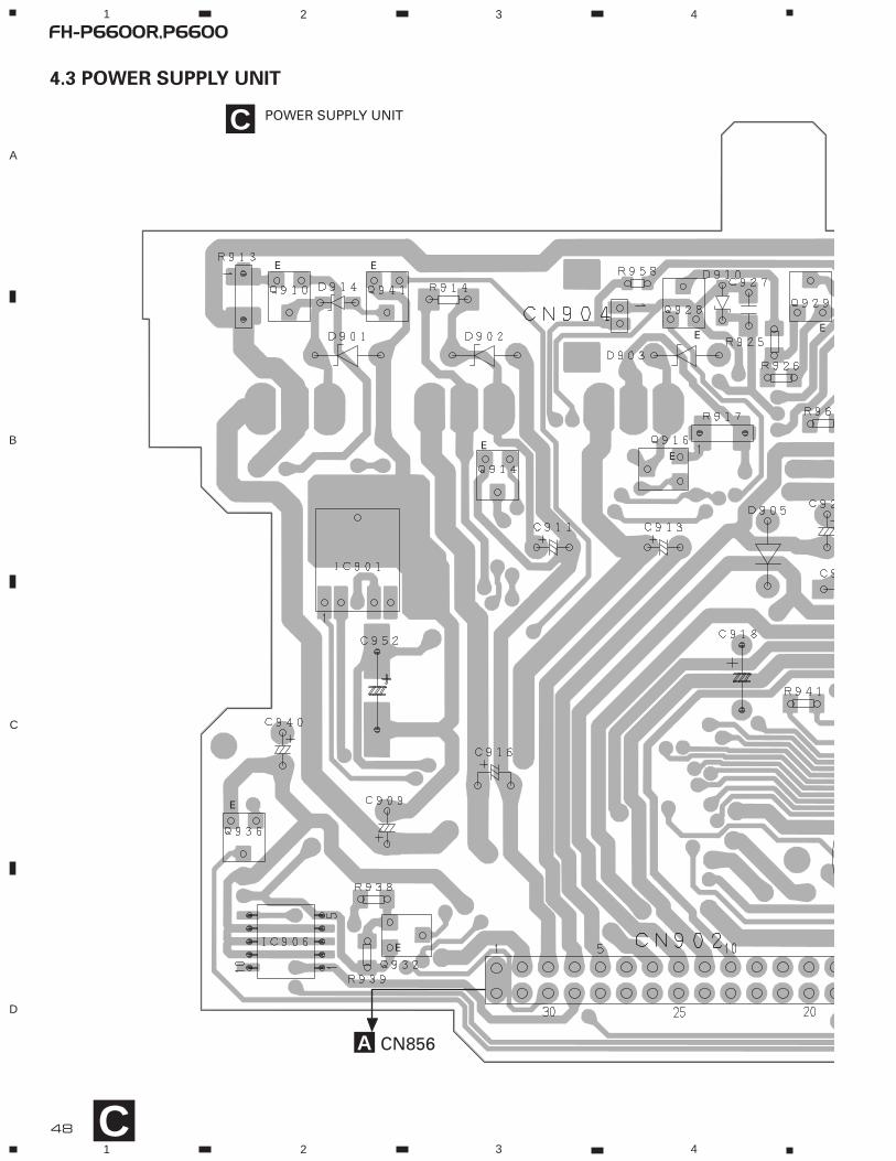
4.3 POWER SUPPLY UNIT
C POWER SUPPLY UNIT
C

49
FH-P6600R,P6600
E
EE
RCA CORD
CN857A
IC,Q
5 6 7 8
A
B
C
D
5 6 7 8
C
SIDE A

50
FH-P6600R,P6600
E
E E
E
E
IC,Q
A
1 2 3 4
B
C
D
1 2 3 4C
C POWER SUPPLY UNIT

51
FH-P6600R,P6600
E
EE E E
E
E
E
E
5 6 7 8
A
B
C
D
5 6 7 8C
SIDE B

52
FH-P6600R,P6600
A
1 2 3 4
B
C
D
1 2 3 4
4.4 FLAP PCB
D
D
CN1201E
CD
EJE
CT
D.F
UN
C
RE
SE
T AN
GLE
SO
UR
CE
+
SO
UR
CE
-
TAP
TY
12
35
64
DIS
PLA
YC
OLO
R
VO
LUM
E-
VO
LUM
E+
BA
ND
DS
P
AU
DIOTA
PE
EJE
CT
FUN
CT
ION
SIDE AFLAP PCB
IC,Q

53
FH-P6600R,P66001 2 3 4
A
B
C
D
1 2 3 4D
EE
E
CN1102F
AD
J PO
INT
V5
VS
S
IC,Q
SIDE BD FLAP PCB
IC,Q

54
FH-P6600R,P6600
A
1 2 3 4
B
C
D
1 2 3 4
4.5 LED PCB
DCN1902
E LED PCB E LED PCB
E
SIDE A SIDE B

55
FH-P6600R,P6600
ACN854
DCN1901
IL1101 IL1102
1 2 3 4
A
B
C
D
1 2 3 4F
4.6 PANEL PCB UNIT
F PANEL PCB UNIT
F PANEL PCB UNIT
CASSETTE DOOR
DETECTOR
FE
RE
FO
HO
ME
CO
NT
RO
L U
NIT
(S8T
X)
M1
CA
RR
IAG
E M
OT
OR
M2
LOA
DIN
G M
OT
OR
M3
SP
IND
LE M
OT
OR
PIC
KU
P U
NIT
(SE
RV
ICE
)(P
8)
CN
802
3 2 1
PH
OT
O U
NIT
(S8)
A
56
FH-P6600R,P6600
A
1 2 3 4
B
C
D
1 2 3 4
4.7 CD MECHANISM MODULE
CN
141
G H
G
G H
SIDE A
H
AC
N25
1

CLA
MP
57
FH-P6600R,P66001 2 3 4
A
B
C
D
1 2 3 4
G
SIDE B
CO
NT
RO
L U
NIT
(S8T
X)
G

IC,Q
IC251
Q351Q352
ADJ
VR302
VR301
IC253
CN252
CN254
CN253CN255
M1M2HEAD ASSY
CN256
2122
Q271
58
FH-P6600R,P6600
A
1 2 3 4
B
C
D
1 2 3 4
A CN111
4.8 CASSETTE MECHANISM MODULE
J
I
SIDE A
SIDE B
CN251
DECK UNITI
DECK UNITI

59
FH-P6600R,P66001 2 3 4
A
B
C
D
1 2 3 4
J
J
123456
S370µs SW
S1LOAD SW
S2MODE SW
CN256
EGN1REEL SENSE
REEL SENSE PCB
CN253I

60
FH-P6600R,P6600
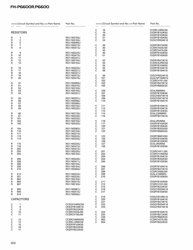
5. ELECTRICAL PARTS LIST
NOTES:
- Parts whose parts numbers are omitted are subject to being not supplied.
- The part numbers shown below indicate chip components.
Chip Resistor
RS1/_S___J,RS1/__S___J
Chip Capacitor (except for CQS.....)
CKS....., CCS....., CSZS.....
=====Circuit Symbol and No.===Part Name Part No.--- ------ ------------------------------------------ -------------------------
Unit Number : CWE1500(FH-P6600R/EW)Unit Name : FM/AM Tuner Unit
MISCELLANEOUS
IC 1 IC PML002AIC 2 IC PM4008AIC 3 IC BR9010FVQ 1 Transistor 2SC4081Q 2 Transistor DTC124EU
Q 3 FET 3SK263Q 51 Transistor 2SC4081Q 201 FET 2SK932Q 202 Transistor DTC124EUQ 204 Transistor 2SC4081
D 1 Diode KV1410(23)D 2 Diode 1SV248D 4 Diode KV1410(23)D 6 Diode KV1410(23)D 101 Diode 1SS355
D 201 Diode DAN217UD 202 Diode DAN217UD 903 Diode KV1410(23)D 904 Diode SVC253L 1 Coil CTC1155
L 2 Coil CTC1155L 3 Inductor LCTB100K2125L 4 Coil CTC1155L 201 Inductor LCTB330M1608L 202 Inductor CTF1287
L 203 Inductor LCTA121J3225L 901 Coil CTC1154L 902 Inductor LCTA3R3J3225L 904 Inductor LCTBR47M1608L 905 Inductor LCTBR47M1608
T 51 Coil CTE1132CF 51 Ceramic Filter CTF1442CF 52 Ceramic Filter CTF1442CF 53 Ceramic Filter CTF1442CF 202 Ceramic Filter CTF1348
X 901 Crystal Resonator 10.250MHz CSS1432
RESISTORS
R 1 RS1/16S153JR 2 RS1/16S103JR 6 RS1/16S103JR 7 RS1/16S273JR 8 RS1/16S473J
R 9 RS1/16S223JR 10 RS1/16S473JR 11 RS1/16S221JR 12 RS1/16S103JR 13 RS1/16S104J
R 16 RS1/16S223JR 17 RS1/16S221JR 18 RS1/16S221JR 19 RS1/16S473JR 20 RS1/16S470J
R 51 RS1/16S470JR 52 RS1/16S103JR 53 RS1/16S103JR 54 RS1/16S331JR 55 RS1/16S331J
R 56 RS1/16S560JR 57 RS1/16S560JR 58 RS1/16S102JR 59 RS1/16S225JR 60 RS1/16S133J
R 61 RS1/16S433JR 62 RS1/16S562JR 101 RS1/16S333JR 102 RS1/16S103JR 103 RS1/16S333J
R 104 RS1/16S562JR 110 RS1/16S154JR 111 RS1/16S273JR 112 RS1/16S223JR 113 RS1/16S222J
R 114 RS1/16S333JR 115 RS1/16S334JR 116 RS1/16S473JR 117 RS1/16S333JR 118 RS1/16S223J
R 122 RS1/16S0R0JR 202 RS1/16S472JR 203 RS1/16S225JR 204 RS1/16S102JR 205 RS1/16S220J
R 206 RS1/16S471JR 208 RS1/16S104JR 209 RS1/16S104JR 210 RS1/16S563JR 213 RS1/16S223J
R 251 RS1/16S225JR 902 RS1/16S103JR 904 RS1/16S473JR 907 RS1/16S103JR 908 RS1/16S681J
R 909 RS1/16S473JR 914 RS1/16S562J
CAPACITORS
C 1 CCSQCH5R0C50C 2 CCSRCH5R0C50C 4 CCSRCJ3R0C50C 6 CKSQYB105K10C 8 CKSRYB222K50
=====Circuit Symbol and No.===Part Name Part No.--- ------ ------------------------------------------ -------------------------
B

61
FH-P6600R,P6600
C 10 CCSRCH220J50C 11 CCSRCH150J50C 12 CCSRCH8R0D50C 14 CCSRCJ3R0C50C 15 CKSRYB103K50
C 16 CKSRYB222K50C 17 CKSRYB222K50C 18 CCSRCJ3R0C50C 19 CKSRYB103K50C 20 CKSRYB103K50
C 21 CKSRYB103K50C 24 CKSQYB334K16C 31 CKSRYB222K50C 32 CCSRCH470J50C 35 CKSRYB103K50
C 51 CKSRYB103K50C 52 CKSRYB473K16C 53 CCSRCK2R0C50C 54 CKSRYB103K50C 55 CKSRYB104K16
C 56 CKSRYB104K16C 58 CKSQYB224K16C 59 CKSRYB223K25C 60 CKSRYB104K16C 101 CEALNP100M10
C 102 CCSRCH151J50C 103 CKSRYB473K16C 105 CKSRYB682K25C 106 CEAL2R2M50C 107 CKSRYB103K50
C 108 CKSQYB474K16C 109 CKSQYB474K16C 110 CKSRYB104K16C 111 CKSRYB104K16C 112 CKSRYB104K16
C 113 CKSRYB123K25C 114 CEAL220M6R3C 115 CKSRYB473K16C 116 CEAL2R2M50C 117 CKSRYB102K50
C 120 CKSRYB153K25C 121 CKSRYB332K50C 122 CKSRYB682K25C 123 CKSRYB681K50C 125 CKSRYB103K50
C 126 CKSRYB103K50C 127 CEAL2R2M50C 128 CKSRYB103K50C 201 CCSRCH471J50C 202 CCSRCH100D50
C 203 CKSRYB104K16C 204 CKSRYB332K50C 205 CKSRYB103K50C 206 CKSRYB104K16C 207 CKSRYB473K16
C 208 CCSRCH560J50C 209 CEAL470M6R3C 210 CKSRYB103K50C 211 CKSRYB103K50C 212 CCSRCH101J50
C 215 CKSRYB223K25C 216 CKSQYB334K16C 217 CKSRYB103K50C 219 CKSQYB105K10C 220 CKSRYB104K16
C 221 CKSRYB473K16C 222 CKSQYB334K16C 223 CKSQYB474K16C 224 CKSRYB104K16C 225 CKSRYB272K50
C 226 CKSRYB682K25C 902 CCSRCH270J50C 904 CKSRYB223K25C 905 CKSRYB103K50C 906 CCSRTH100D50
C 907 CCSRTH150J50C 909 CCSRTH100D50C 910 CKSRYB332K50C 912 CKSQYB474K16C 913 CKSRYB223K25
C 914 CKSRYB682K25C 915 CKSQYB223K25C 916 CKSQYB474K16C 917 CKSYB475K10C 918 CKSRYB223K25
C 919 CKSQYB225K10C 920 CCSRCH270J50C 921 CCSRCH270J50C 922 CKSYB105K16C 923 CKSRYB103K50
Unit Number : CWE1501(FH-P6600/ES)Unit Name : FM/AM Tuner Unit
MISCELLANEOUS
IC 1 IC PML002AIC 2 IC PM4008AIC 3 IC BR9010FVQ 1 Transistor 2SC4081Q 2 Transistor DTC124EU
Q 3 FET 3SK263Q 51 Transistor 2SC4081Q 201 FET 2SK932Q 202 Transistor DTC124EUQ 204 Transistor 2SC4081
D 1 Diode KV1410(23)D 2 Diode 1SV248D 6 Diode KV1410(23)D 201 Diode DAN217UD 202 Diode MA147
D 903 Diode KV1410(23)D 904 Diode SVC253L 1 Coil CTC1155L 3 Inductor LCTB1R5K2125L 4 Coil CTC1155
L 201 Inductor LCTB330K1608L 202 Inductor LFEA102JL 203 Inductor LCTA121J3225L 901 Coil CTC1154L 902 Inductor LCTA3R3J3225
L 904 Inductor LCTBR47K1608L 905 Inductor LCTBR47K1608T 51 Coil CTE1132CF 51 Ceramic Filter CTF1442CF 52 Ceramic Filter CTF1442
CF 53 Ceramic Filter CTF1442CF 202 Ceramic Filter CTF1476X 901 Crystal Resonator 10.250MHz CSS1432
=====Circuit Symbol and No.===Part Name Part No.--- ------ ------------------------------------------ -------------------------
=====Circuit Symbol and No.===Part Name Part No.--- ------ ------------------------------------------ -------------------------
B
62
FH-P6600R,P6600
RESISTORS
R 1 RS1/16S183JR 2 RS1/16S103JR 5 RS1/16S0R0JR 7 RS1/16S273JR 8 RS1/16S473J
R 9 RS1/16S223JR 10 RS1/16S473JR 11 RS1/16S221JR 12 RS1/16S103JR 13 RS1/16S104J
R 16 RS1/16S223JR 17 RS1/16S221JR 18 RS1/16S221JR 19 RS1/16S473JR 20 RS1/16S470J
R 31 RS1/16S0R0JR 51 RS1/16S470JR 52 RS1/16S103JR 53 RS1/16S103JR 54 RS1/16S331J
R 55 RS1/16S331JR 56 RS1/16S560JR 57 RS1/16S560JR 58 RS1/16S102JR 59 RS1/16S225J
R 60 RS1/16S133JR 61 RS1/16S433JR 101 RS1/16S333JR 102 RS1/16S103JR 103 RS1/16S333J
R 104 RS1/16S562JR 110 RS1/16S154JR 111 RS1/16S273JR 113 RS1/16S222JR 114 RS1/16S333J
R 115 RS1/16S334JR 116 RS1/16S473JR 202 RS1/16S472JR 203 RS1/16S225JR 204 RS1/16S102J
R 205 RS1/16S220JR 206 RS1/16S471JR 208 RS1/16S104JR 209 RS1/16S104JR 210 RS1/16S563J
R 213 RS1/16S223JR 251 RS1/16S225JR 902 RS1/16S103JR 904 RS1/16S473JR 907 RS1/16S103J
R 908 RS1/16S681JR 909 RS1/16S473JR 914 RS1/16S562J
CAPACITORS
C 1 CCSQCH4R0C50C 6 CKSQYB105K10C 8 CKSRYB222K50C 10 CCSRCH220J50C 11 CCSRCH150J50
C 12 CCSRCH8R0D50C 14 CCSRCJ3R0C50C 15 CKSRYB103K50C 16 CKSRYB222K50C 17 CKSRYB222K50
C 18 CCSRCJ3R0C50C 19 CKSRYB103K50C 20 CKSRYB103K50C 21 CKSRYB103K50C 24 CKSQYB334K16
C 26 CKSRYB472K50C 30 CCSRCH220J50C 32 CCSRCH470J50C 35 CKSRYB103K50C 51 CKSRYB103K50
C 52 CKSRYB473K16C 53 CCSRCK2R0C50C 54 CKSRYB103K50C 55 CKSRYB104K16C 56 CKSRYB104K16
C 58 CKSQYB224K16C 101 CEALNP100M10C 102 CCSRCH151J50C 103 CKSRYB473K16C 105 CKSRYB682K25
C 106 CEALR68M50C 107 CKSRYB103K50C 108 CKSQYB474K16C 109 CKSQYB474K16C 110 CKSRYB104K16
C 111 CKSRYB104K16C 112 CKSRYB104K16C 113 CKSRYB123K25C 114 CEAL220M6R3C 115 CKSRYB473K16
C 116 CEAL2R2M50C 117 CKSRYB102K50C 120 CKSRYB183K25C 121 CKSRYB332K50C 122 CKSRYB562K25
C 123 CKSRYB681K50C 125 CKSRYB103K50C 126 CKSRYB103K50C 127 CEAL2R2M50C 128 CKSRYB103K50
C 201 CCSRCH471J50C 202 CCSRCH100D50C 203 CKSRYB104K16C 204 CKSRYB332K50C 205 CKSRYB103K50
C 206 CKSRYB104K16C 207 CKSRYB473K16C 208 CCSRCH560J50C 209 CEAL470M6R3C 210 CKSRYB103K50
C 211 CKSRYB103K50C 212 CCSRCH101J50C 215 CKSRYB223K25C 216 CKSQYB334K16C 217 CKSRYB103K50
C 219 CKSQYB105K10C 220 CKSRYB104K16C 221 CKSRYB473K16C 222 CKSQYB334K16C 223 CKSQYB474K16
C 224 CKSRYB104K16C 225 CKSRYB272K50C 226 CKSRYB682K25C 902 CCSRCH270J50C 904 CKSRYB223K25
=====Circuit Symbol and No.===Part Name Part No.--- ------ ------------------------------------------ -------------------------
=====Circuit Symbol and No.===Part Name Part No.--- ------ ------------------------------------------ -------------------------
63
FH-P6600R,P6600
C 905 CKSRYB103K50C 906 CCSRTH100D50C 907 CCSRTH150J50C 909 CCSRTH100D50C 910 CKSRYB332K50
C 912 CKSQYB474K16C 913 CKSRYB223K25C 914 CKSRYB682K25C 915 CKSQYB223K25C 916 CKSQYB474K16
C 917 CKSYB475K10C 918 CKSRYB223K25C 919 CKSQYB225K10C 920 CCSRCH270J50C 921 CCSRCH270J50
C 922 CKSYB105K16C 923 CKSRYB103K50
Unit Number : CWM7006(FH-P6600R/EW)Unit Name : Audio Amp Unit
MISCELLANEOUS
IC 151 IC BA3131FSIC 153 IC NJM4558MDIC 251 IC PDG255AIC 252 IC TC74VHC125FTIC 253 IC TC7SET08FU
IC 301 IC PM0017AMIC 302 IC NJM4558MDIC 303 IC NJM4558MDIC 304 IC NJM4558MDIC 351 IC PAL005A
IC 501 IC PM4009AIC 601 IC PE5124AIC 602 IC S-80734ANDYIIC 801 IC TC7W14FUIC 803 Photo-interrupter GP1S94J
IC 804 Photo-interrupter GP1S94JIC 805 IC BA6288FSIC 806 IC BA09SFPQ 251 Transistor IMH1AQ 351 Transistor DTC144EK
Q 352 Transistor DTC144EUQ 401 Transistor 2SC2412KQ 402 Transistor 2SC2412KQ 403 Transistor 2SD1757KQ 404 Transistor 2SD1757K
Q 405 Transistor 2SC2412KQ 406 Transistor IMH3AQ 407 Transistor DTA114EKQ 408 Transistor DTA124EKQ 501 Transistor DTA124EK
Q 851 Transistor 2SC2412KQ 852 Transistor 2SC2412KQ 853 Transistor DTC124EKQ 854 Transistor 2SA1162Q 855 Chip Transistor 2SC2712
Q 856 Chip Transistor 2SC2712Q 871 Transistor 2SA1036KQ 872 Transistor 2SB1132Q 873 Transistor DTC124EUQ 874 Transistor 2SB1132
Q 875 Transistor DTC124EUD 111 Diode 1SS133D 351 Diode MA152WKD 601 Diode MA110D 801 Diode 1SS133
D 802 Diode 1SS133D 851 Diode MA3082(L)D 852 Diode ERA15-02VHD 853 Diode ERA15-02VHD 854 Diode ERA15-02VH
D 855 Diode ERA15-02VHD 856 Diode ERA15-02VHD 857 Diode ERA15-02VHD 858 Diode ERA15-02VHD 859 Diode MA3062(H)
D 860 Diode MA3082(L)ZNR 451 Surge Protector DSPS-201M-S00BL 141 Inductor CTF1306L 142 Inductor CTF1306L 143 Inductor CTF1306
L 251 Inductor LCTA101J3225L 252 Inductor CTF1379L 253 Inductor CTF1305L 254 Inductor CTF1379L 255 Inductor CTF1379
L 256 Inductor CTF1379L 257 Inductor CTF1379L 258 Inductor CTF1379L 259 Inductor CTF1379L 260 Inductor CTF1379
L 261 Inductor CTF1379L 262 Inductor LCTA471J3225L 263 Inductor CTF1379L 264 Inductor CTF1379L 265 Inductor CTF1379
L 401 Ferri-Inductor LAU4R7KL 402 Inductor LCTA101J3225L 403 Inductor CTF1379L 404 Inductor LCTA4R7J3225L 405 Inductor CTF1379
L 406 Inductor CTF1379L 407 Inductor CTF1379L 408 Inductor CTF1379L 409 Inductor CTF1379L 410 Inductor CTF1379
L 411 Inductor CTF1379L 412 Inductor CTF1379L 414 Inductor CTF1379L 501 Inductor LCTA101J3225L 502 Inductor LCTA101J3225
L 503 Inductor CTF1379L 504 Inductor CTF1379L 601 Inductor CTF1379L 602 Inductor CTF1379L 603 Inductor LCTB4R7K2125
L 604 Inductor CTF1379L 605 Inductor CTF1379L 606 Inductor CTF1379L 607 Inductor CTF1379L 608 Inductor CTF1379
L 609 Inductor CTF1379L 610 Inductor CTF1379L 611 Inductor CTF1379L 612 Inductor CTF1379L 613 Inductor CTF1379
L 614 Inductor CTF1379L 616 Inductor CTF1379L 617 Inductor CTF1379L 618 Inductor CTF1379L 619 Inductor CTF1379
=====Circuit Symbol and No.===Part Name Part No.--- ------ ------------------------------------------ -------------------------
=====Circuit Symbol and No.===Part Name Part No.--- ------ ------------------------------------------ -------------------------
A

64
FH-P6600R,P6600
L 620 Inductor CTF1379L 621 Inductor CTF1379L 622 Inductor CTF1379L 851 Inductor CTF1379L 852 Inductor CTF1379
L 871 Inductor CTF1379L 872 Inductor CTF1379L 873 Inductor CTF1379L 874 Inductor CTF1379L 875 Inductor CTF1379
L 876 Inductor CTF1379L 877 Inductor CTF1379L 878 Inductor CTF1379L 879 Inductor CTF1379L 880 Inductor CTF1379
L 881 Inductor CTF1379L 882 Inductor CTF1379TH 601 Thermistor CCX1037X 251 Radiator 16.9344MHz CSS1463X 501 Crystal Resonator 3.648MHz CSS1447
X 601 Radiator 6.291456MHz CSS1505S 801 Spring Switch(FEJ) CSN1046S 802 Spring Switch(FOPN) CSN1046S 803 Spring Switch(FCLS) CSN1046FU 851 Micro-Fuse 4A CEK1199
FU 871 Micro-Fuse 800mA CEK1206FU 872 Micro-Fuse 200mA CEK1189
FM/AM Tuner Unit CWE1500
RESISTORS
R 111 RS1/16S102JR 112 RS1/16S102JR 113 RAB4C222JR 114 RS1/16S473JR 115 RS1/16S473J
R 117 RS1/16S681JR 118 RAB4C222JR 119 RA3C222JR 120 RS1/16S473JR 121 RS1/16S473J
R 122 RS1/16S473JR 123 RS1/16S473JR 131 RS1/10S222JR 132 RS1/10S101JR 133 RS1/10S101J
R 134 RS1/10S620JR 141 RS1/16S681JR 142 RA3C102JR 143 RS1/16S471JR 144 RS1/16S471J
R 145 RS1/16S471JR 151 RS1/16S473JR 152 RS1/16S473JR 153 RS1/16S473JR 154 RS1/16S473J
R 155 RS1/16S392JR 156 RS1/16S392JR 157 RS1/16S203JR 158 RS1/16S203JR 159 RS1/16S102J
R 160 RS1/16S102JR 161 RS1/16S223JR 162 RS1/16S223JR 163 RS1/16S472JR 164 RS1/16S472J
R 165 RS1/16S223JR 166 RS1/16S223JR 173 RS1/16S473JR 174 RS1/16S473JR 179 RS1/16S472J
R 180 RS1/16S472JR 181 RS1/16S123JR 182 RS1/16S123JR 183 RS1/16S0R0JR 184 RS1/16S0R0J
R 251 RS1/16S221JR 252 RS1/16S221JR 253 RAB4C221JR 254 RS1/16S225JR 255 RS1/16S102J
R 256 RS1/16S102JR 257 RS1/16S221JR 259 RS1/16S102JR 263 RS1/16S331JR 264 RS1/16S473J
R 265 RS1/16S473JR 266 RS1/16S155JR 301 RS1/16S103JR 302 RS1/16S103JR 303 RS1/16S103J
R 304 RS1/16S103JR 305 RN1/16SE1202DR 306 RN1/16SE1202DR 307 RS1/16S153JR 308 RS1/16S153J
R 309 RS1/16S273JR 310 RS1/16S273JR 311 RS1/16S243JR 312 RS1/16S243JR 313 RS1/16S333J
R 314 RS1/16S333JR 315 RN1/16SE1202DR 316 RN1/16SE1202DR 317 RS1/16S153JR 318 RS1/16S153J
R 319 RS1/16S273JR 320 RS1/16S273JR 321 RS1/16S243JR 322 RS1/16S243JR 323 RS1/16S333J
R 324 RS1/16S333JR 325 RN1/16SE1202DR 326 RN1/16SE1202DR 327 RS1/16S153JR 328 RS1/16S153J
R 329 RS1/16S273JR 330 RS1/16S273JR 331 RS1/16S243JR 332 RS1/16S243JR 333 RS1/16S333J
R 334 RS1/16S333JR 335 RS1/16S474JR 336 RS1/16S474JR 337 RS1/16S474JR 338 RS1/16S474J
R 339 RS1/16S474JR 340 RS1/16S474JR 351 RS1/10S103JR 352 RS1/10S103JR 353 RS1/16S103J
=====Circuit Symbol and No.===Part Name Part No.--- ------ ------------------------------------------ -------------------------
=====Circuit Symbol and No.===Part Name Part No.--- ------ ------------------------------------------ -------------------------

65
FH-P6600R,P6600
R 354 RS1/10S331JR 355 RS1/16S103JR 356 RS1/10S473JR 357 RS1/16S221JR 358 RS1/16S221J
R 359 RS1/16S221JR 401 RS1/16S0R0JR 402 RS1/16S473JR 403 RS1/16S473JR 404 RS1/16S473J
R 405 RS1/16S681JR 406 RS1/16S103JR 407 RS1/16S681JR 408 RS1/16S681JR 409 RS1/16S681J
R 410 RS1/16S681JR 411 RS1/16S681JR 412 RS1/16S681JR 413 RS1/16S393JR 414 RS1/16S153J
R 415 RS1/16S162JR 416 RS1/16S162JR 417 RS1/16S272JR 418 RS1/16S272JR 419 RS1/16S473J
R 420 RS1/16S473JR 421 RS1/16S472JR 422 RS1/16S473JR 425 RS1/16S473JR 427 RS1/16S224J
R 428 RS1/16S222JR 429 RS1/16S224JR 430 RS1/16S224JR 431 RS1/16S222JR 432 RS1/16S222J
R 433 RS1/16S222JR 434 RS1/16S473JR 435 RS1/16S223JR 436 RS1/16S223JR 437 RS1/16S681J
R 438 RS1/16S681JR 441 RS1/16S102JR 442 RS1/16S474JR 447 RS1/16S681JR 501 RS1/16S102J
R 502 RS1/16S102JR 503 RS1/16S102JR 507 RS1/16S0R0JR 508 RS1/16S0R0JR 511 RS1/16S102J
R 512 RS1/16S0R0JR 513 RS1/16S225JR 518 RS1/16S102JR 601 RS1/16S473JR 602 RS1/16S473J
R 603 RS1/16S0R0JR 604 RS1/8S222JR 605 RS1/16S0R0JR 606 RS1/16S0R0JR 607 RS1/16S472J
R 608 RS1/16S473JR 609 RS1/16S221JR 610 RS1/16S0R0JR 611 RS1/16S221JR 612 RS1/16S0R0J
R 613 RS1/16S473JR 614 RS1/16S222JR 615 RS1/16S473JR 616 RS1/16S473JR 617 RS1/16S473J
R 618 RS1/16S473JR 619 RS1/16S102JR 620 RN1/16SE2202DR 622 RS1/16S222JR 623 RS1/16S222J
R 624 RS1/16S473JR 626 RS1/16S102JR 627 RS1/16S102JR 628 RS1/16S473JR 629 RS1/16S473J
R 634 RS1/16S473JR 635 RS1/16S473JR 636 RS1/16S473JR 637 RA3C473JR 638 RS1/16S102J
R 639 RS1/16S124JR 640 RS1/16S0R0JR 641 RS1/16S0R0JR 643 RS1/16S473JR 644 RS1/16S472J
R 645 RS1/16S222JR 646 RS1/16S104JR 647 RS1/16S104JR 648 RS1/16S221JR 649 RS1/16S221J
R 650 RS1/16S473JR 801 RS1/16S221JR 802 RS1/16S221JR 803 RS1/16S221JR 804 RS1/16S473J
R 805 RS1/16S221JR 806 RS1/16S473JR 807 RS1/16S102JR 808 RS1/16S102JR 851 RS1/16S103J
R 852 RS1/10S472JR 853 RS1/16S473JR 854 RS1/16S224JR 855 RS1/8S101JR 856 RS1/10S102J
R 857 RS1/10S223JR 858 RS1/10S473JR 859 RS1/10S223JR 860 RS1/10S103JR 861 RS1/10S473J
R 862 RS1/10S473JR 863 RS1/10S472JR 871 RS1/10S223JR 872 RS1/10S152JR 873 RS1/16S102J
R 874 RS1/10S332JR 875 RS1/10S223JR 876 RS1/8S222JR 877 RS1/10S222JR 888 RS1/16S102J
R 889 RS1/16S102JR 890 RS1/16S102JR 891 RS1/16S102JR 892 RS1/16S102JR 893 RS1/16S102J
=====Circuit Symbol and No.===Part Name Part No.--- ------ ------------------------------------------ -------------------------
=====Circuit Symbol and No.===Part Name Part No.--- ------ ------------------------------------------ -------------------------

CAPACITORS
C 113 CEJA220M16C 114 CEJA100M16C 131 CKSRYB104K16C 141 CKSYB222K50C 151 CKSYB105K16
C 152 CKSYB105K16C 153 CKSYB475K10C 154 CKSYB475K10C 155 CKSYB475K10C 156 CKSYB475K10
C 157 CCSRCH101J50C 158 CCSRCH101J50C 161 CKSQYB223K25C 162 CEV100M16C 163 CEV220M10
C 164 CEV101M10C 165 CCSRCH681J50C 166 CCSRCH681J50C 167 CCSRCH271J50C 168 CCSRCH271J50
C 169 CEVNP100M16C 170 CEVNP100M16C 172 CKSYB475K10C 179 CEJA100M16C 184 CEJA100M16
C 251 CKSYB106K6R3C 252 CKSRYB104K16C 253 CKSRYB104K16C 254 CKSRYB104K16C 255 CKSRYB104K16
C 256 CKSRYB104K16C 257 CKSRYB104K16C 258 CKSRYB104K16C 259 CKSRYB104K16C 260 CKSRYB104K16
C 261 CKSRYB104K16C 262 CKSRYB104K16C 263 CKSRYB104K16C 264 CKSRYB104K16C 265 CKSRYB104K16
C 266 CKSRYB104K16C 267 CKSRYB104K16C 268 CCSRCH180J50C 269 CCSRCH180J50C 270 CKSYB475K10
C 271 CEV101M4C 273 CKSYB475K10C 274 CKSRYB102K50C 275 CKSRYB102K50C 276 CCSRCH560J50
C 277 CKSRYB103K25C 278 CKSRYB103K25C 280 CEV221M4C 281 CCSRCH101J50C 282 CKSRYB103K25
C 301 CKSYB105K16C 302 CKSYB105K16C 303 CKSYB105K16C 304 CKSYB105K16C 305 CKSYB105K16
C 306 CKSYB105K16C 307 CEJA100M16C 308 CEJA100M16C 309 CCSRCH271J50C 310 CCSRCH271J50
C 311 CCSRCH121J50C 312 CCSRCH121J50C 313 CCSRCH101J50C 314 CCSRCH101J50C 315 CKSYB475K10
C 316 CKSYB475K10C 317 CCSRCH271J50C 318 CCSRCH271J50C 319 CCSRCH121J50C 320 CCSRCH121J50
C 321 CCSRCH101J50C 322 CCSRCH101J50C 323 CKSYB475K10C 324 CKSYB475K10C 325 CCSRCH271J50
C 326 CCSRCH271J50C 327 CCSRCH121J50C 328 CCSRCH121J50C 329 CCSRCH101J50C 330 CCSRCH101J50
C 331 CKSYB475K10C 332 CKSYB475K10C 333 CKSYB106K6R3C 334 CKSRYB104K16C 335 CKSQYB474K16
C 336 CKSQYB474K16C 337 CKSYB474K16C 338 CKSYB474K16C 339 CKSYB474K16C 340 CKSYB474K16
C 341 CKSQYB474K16C 342 CKSQYB474K16C 343 CKSQYB225K10C 344 CKSQYB225K10C 345 CKSQYB225K10
C 346 CKSQYB225K10C 347 CKSQYB225K10C 348 CKSQYB225K10C 349 CKSYB475K10C 350 CKSQYB105K16
C 351 CEJA330M10C 352 CKSQYB105K16C 353 4700µF/16V CCH1302C 354 CKSYB104K50C 355 CEV100M16
C 356 CKSYB225K16C 357 CKSYB225K16C 401 CKSRYB103K25C 402 CKSRYB182K50C 404 CKSRYB473K16
C 405 CEJA101M10C 406 CKSRYB103K25C 407 CKSRYB123K25C 408 CKSRYB123K25C 409 CKSRYB472K50
C 410 CEJA220M10C 411 CKSRYB223K25C 412 CKSRYB223K25C 413 CKSQYB105K16C 414 CKSQYB105K16
C 415 CKSQYB472K50C 417 CKSRYB223K25C 422 CCSRCH101J50C 424 CCSRCH101J50C 425 CKSRYB104K16
66
FH-P6600R,P6600
=====Circuit Symbol and No.===Part Name Part No.--- ------ ------------------------------------------ -------------------------
=====Circuit Symbol and No.===Part Name Part No.--- ------ ------------------------------------------ -------------------------
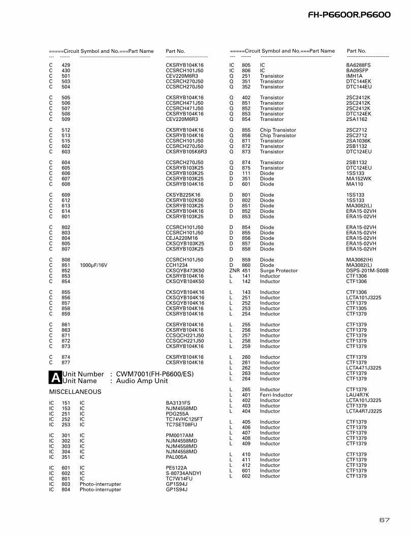
C 429 CKSRYB104K16C 430 CCSRCH101J50C 501 CEV220M6R3C 503 CCSRCH270J50C 504 CCSRCH270J50
C 505 CKSRYB104K16C 506 CCSRCH471J50C 507 CCSRCH471J50C 508 CKSRYB104K16C 509 CEV220M6R3
C 512 CKSRYB104K16C 513 CKSRYB104K16C 515 CCSRCH101J50C 602 CCSRCH270J50C 603 CKSRYB105K6R3
C 604 CCSRCH270J50C 605 CKSRYB103K25C 606 CKSRYB103K25C 607 CKSRYB103K25C 608 CKSRYB104K16
C 609 CKSYB225K16C 612 CKSRYB102K50C 613 CKSRYB103K25C 614 CKSRYB104K16C 801 CKSRYB103K25
C 802 CCSRCH101J50C 803 CCSRCH101J50C 804 CEJA220M16C 805 CKSQYB103K25C 807 CKSRYB103K25
C 808 CCSRCH101J50C 851 1000µF/16V CCH1234C 852 CKSQYB473K50C 853 CKSRYB104K16C 854 CKSQYB104K50
C 855 CKSQYB104K16C 856 CKSQYB104K16C 857 CKSQYB104K16C 858 CKSRYB104K16C 859 CKSRYB104K16
C 861 CKSRYB104K16C 863 CKSRYB104K16C 871 CCSQCH221J50C 872 CCSQCH221J50C 873 CKSRYB104K16
C 874 CKSRYB104K16C 877 CKSRYB104K16
Unit Number : CWM7001(FH-P6600/ES)Unit Name : Audio Amp Unit
MISCELLANEOUS
IC 151 IC BA3131FSIC 153 IC NJM4558MDIC 251 IC PDG255AIC 252 IC TC74VHC125FTIC 253 IC TC7SET08FU
IC 301 IC PM0017AMIC 302 IC NJM4558MDIC 303 IC NJM4558MDIC 304 IC NJM4558MDIC 351 IC PAL005A
IC 601 IC PE5122AIC 602 IC S-80734ANDYIIC 801 IC TC7W14FUIC 803 Photo-interrupter GP1S94JIC 804 Photo-interrupter GP1S94J
IC 805 IC BA6288FSIC 806 IC BA09SFPQ 251 Transistor IMH1AQ 351 Transistor DTC144EKQ 352 Transistor DTC144EU
Q 402 Transistor 2SC2412KQ 851 Transistor 2SC2412KQ 852 Transistor 2SC2412KQ 853 Transistor DTC124EKQ 854 Transistor 2SA1162
Q 855 Chip Transistor 2SC2712Q 856 Chip Transistor 2SC2712Q 871 Transistor 2SA1036KQ 872 Transistor 2SB1132Q 873 Transistor DTC124EU
Q 874 Transistor 2SB1132Q 875 Transistor DTC124EUD 111 Diode 1SS133D 351 Diode MA152WKD 601 Diode MA110
D 801 Diode 1SS133D 802 Diode 1SS133D 851 Diode MA3082(L)D 852 Diode ERA15-02VHD 853 Diode ERA15-02VH
D 854 Diode ERA15-02VHD 855 Diode ERA15-02VHD 856 Diode ERA15-02VHD 857 Diode ERA15-02VHD 858 Diode ERA15-02VH
D 859 Diode MA3062(H)D 860 Diode MA3082(L)ZNR 451 Surge Protector DSPS-201M-S00BL 141 Inductor CTF1306L 142 Inductor CTF1306
L 143 Inductor CTF1306L 251 Inductor LCTA101J3225L 252 Inductor CTF1379L 253 Inductor CTF1305L 254 Inductor CTF1379
L 255 Inductor CTF1379L 256 Inductor CTF1379L 257 Inductor CTF1379L 258 Inductor CTF1379L 259 Inductor CTF1379
L 260 Inductor CTF1379L 261 Inductor CTF1379L 262 Inductor LCTA471J3225L 263 Inductor CTF1379L 264 Inductor CTF1379
L 265 Inductor CTF1379L 401 Ferri-Inductor LAU4R7KL 402 Inductor LCTA101J3225L 403 Inductor CTF1379L 404 Inductor LCTA4R7J3225
L 405 Inductor CTF1379L 406 Inductor CTF1379L 407 Inductor CTF1379L 408 Inductor CTF1379L 409 Inductor CTF1379
L 410 Inductor CTF1379L 411 Inductor CTF1379L 412 Inductor CTF1379L 601 Inductor CTF1379L 602 Inductor CTF1379
67
FH-P6600R,P6600
=====Circuit Symbol and No.===Part Name Part No.--- ------ ------------------------------------------ -------------------------
=====Circuit Symbol and No.===Part Name Part No.--- ------ ------------------------------------------ -------------------------
A

L 603 Inductor LCTB4R7K2125L 604 Inductor CTF1379L 605 Inductor CTF1379L 606 Inductor CTF1379L 607 Inductor CTF1379
L 608 Inductor CTF1379L 609 Inductor CTF1379L 610 Inductor CTF1379L 611 Inductor CTF1379L 612 Inductor CTF1379
L 613 Inductor CTF1379L 614 Inductor CTF1379L 616 Inductor CTF1379L 617 Inductor CTF1379L 618 Inductor CTF1379
L 619 Inductor CTF1379L 620 Inductor CTF1379L 621 Inductor CTF1379L 622 Inductor CTF1379L 851 Inductor CTF1379
L 852 Inductor CTF1379L 871 Inductor CTF1379L 872 Inductor CTF1379L 873 Inductor CTF1379L 874 Inductor CTF1379
L 875 Inductor CTF1379L 876 Inductor CTF1379L 877 Inductor CTF1379L 878 Inductor CTF1379L 879 Inductor CTF1379
L 880 Inductor CTF1379L 881 Inductor CTF1379L 882 Inductor CTF1379TH 601 Thermistor CCX1037X 251 Radiator 16.9344MHz CSS1463
X 601 Radiator 6.291456MHz CSS1505S 801 Spring Switch(FEJ) CSN1046S 802 Spring Switch(FOPN) CSN1046S 803 Spring Switch(FOLS) CSN1046FU 851 Micro-Fuse 4A CEK1199
FU 871 Micro-Fuse 800mA CEK1206FU 872 Micro-Fuse 200mA CEK1189
FM/AM Tuner Unit CWE1501
RESISTORS
R 111 RS1/16S102JR 112 RS1/16S102JR 113 RAB4C222JR 114 RS1/16S473JR 115 RS1/16S473J
R 117 RS1/16S681JR 118 RAB4C222JR 119 RA3C222JR 120 RS1/16S473JR 121 RS1/16S473J
R 122 RS1/16S473JR 123 RS1/16S473JR 131 RS1/10S222JR 132 RS1/10S101JR 133 RS1/10S101J
R 134 RS1/10S620JR 141 RS1/16S681JR 142 RA3C102JR 143 RS1/16S471JR 144 RS1/16S471J
R 145 RS1/16S471JR 151 RS1/16S473JR 152 RS1/16S473JR 153 RS1/16S473JR 154 RS1/16S473J
R 155 RS1/16S392JR 156 RS1/16S392JR 157 RS1/16S203JR 158 RS1/16S203JR 159 RS1/16S102J
R 160 RS1/16S102JR 161 RS1/16S223JR 162 RS1/16S223JR 163 RS1/16S472JR 164 RS1/16S472J
R 165 RS1/16S223JR 166 RS1/16S223JR 173 RS1/16S473JR 174 RS1/16S473JR 179 RS1/16S472J
R 180 RS1/16S472JR 181 RS1/16S123JR 182 RS1/16S123JR 183 RS1/16S0R0JR 184 RS1/16S0R0J
R 251 RS1/16S221JR 252 RS1/16S221JR 253 RAB4C221JR 254 RS1/16S225JR 255 RS1/16S102J
R 256 RS1/16S102JR 257 RS1/16S221JR 259 RS1/16S102JR 263 RS1/16S331JR 264 RS1/16S473J
R 265 RS1/16S473JR 266 RS1/16S155JR 301 RS1/16S103JR 302 RS1/16S103JR 303 RS1/16S103J
R 304 RS1/16S103JR 305 RN1/16SE1202DR 306 RN1/16SE1202DR 307 RS1/16S153JR 308 RS1/16S153J
R 309 RS1/16S273JR 310 RS1/16S273JR 311 RS1/16S243JR 312 RS1/16S243JR 313 RS1/16S333J
R 314 RS1/16S333JR 315 RN1/16SE1202DR 316 RN1/16SE1202DR 317 RS1/16S153JR 318 RS1/16S153J
R 319 RS1/16S273JR 320 RS1/16S273JR 321 RS1/16S243JR 322 RS1/16S243JR 323 RS1/16S333J
R 324 RS1/16S333JR 325 RN1/16SE1202DR 326 RN1/16SE1202DR 327 RS1/16S153JR 328 RS1/16S153J
=====Circuit Symbol and No.===Part Name Part No.--- ------ ------------------------------------------ -------------------------
68
FH-P6600R,P6600
=====Circuit Symbol and No.===Part Name Part No.--- ------ ------------------------------------------ -------------------------

69
FH-P6600R,P6600
=====Circuit Symbol and No.===Part Name Part No.--- ------ ------------------------------------------ -------------------------
=====Circuit Symbol and No.===Part Name Part No.--- ------ ------------------------------------------ -------------------------
R 329 RS1/16S273JR 330 RS1/16S273JR 331 RS1/16S243JR 332 RS1/16S243JR 333 RS1/16S333J
R 334 RS1/16S333JR 335 RS1/16S474JR 336 RS1/16S474JR 337 RS1/16S474JR 338 RS1/16S474J
R 339 RS1/16S474JR 340 RS1/16S474JR 351 RS1/10S103JR 352 RS1/10S103JR 353 RS1/16S103J
R 354 RS1/10S331JR 355 RS1/16S103JR 356 RS1/10S473JR 357 RS1/16S221JR 358 RS1/16S221J
R 359 RS1/16S221JR 401 RS1/16S0R0JR 403 RS1/16S473JR 404 RS1/16S473JR 405 RS1/16S681J
R 406 RS1/16S103JR 407 RS1/16S681JR 408 RS1/16S681JR 409 RS1/16S681JR 410 RS1/16S681J
R 411 RS1/16S681JR 413 RS1/16S393JR 415 RS1/16S272JR 416 RS1/16S272JR 417 RS1/16S162J
R 418 RS1/16S162JR 419 RS1/16S473JR 420 RS1/16S473JR 421 RS1/16S472JR 422 RS1/16S473J
R 423 RS1/16S0R0JR 424 RS1/16S0R0JR 425 RS1/16S473JR 428 RS1/16S222JR 433 RS1/16S222J
R 440 RS1/16S0R0JR 601 RS1/16S473JR 602 RS1/16S473JR 603 RS1/16S0R0JR 604 RS1/8S222J
R 605 RS1/16S0R0JR 606 RS1/16S0R0JR 607 RS1/16S472JR 608 RS1/16S473JR 609 RS1/16S221J
R 610 RS1/16S0R0JR 611 RS1/16S221JR 612 RS1/16S0R0JR 613 RS1/16S473JR 614 RS1/16S222J
R 615 RS1/16S473JR 616 RS1/16S473JR 617 RS1/16S473JR 618 RS1/16S473JR 619 RS1/16S102J
R 620 RN1/16SE2202DR 622 RS1/16S222JR 623 RS1/16S222JR 624 RS1/16S473JR 625 RS1/16S473J
R 626 RS1/16S102JR 627 RS1/16S102JR 628 RS1/16S473JR 629 RS1/16S473JR 632 RS1/16S0R0J
R 633 RS1/16S0R0JR 634 RS1/16S473JR 635 RS1/16S473JR 636 RS1/16S473JR 637 RA3C473J
R 638 RS1/16S102JR 639 RS1/16S124JR 640 RS1/16S0R0JR 641 RS1/16S0R0JR 643 RS1/16S473J
R 644 RS1/16S472JR 645 RS1/16S222JR 646 RS1/16S104JR 647 RS1/16S104JR 648 RS1/16S221J
R 649 RS1/16S221JR 650 RS1/16S473JR 801 RS1/16S221JR 802 RS1/16S221JR 803 RS1/16S221J
R 804 RS1/16S473JR 805 RS1/16S221JR 806 RS1/16S473JR 807 RS1/16S102JR 808 RS1/16S102J
R 851 RS1/16S103JR 852 RS1/10S472JR 853 RS1/16S473JR 854 RS1/16S224JR 855 RS1/8S101J
R 856 RS1/10S102JR 857 RS1/10S223JR 858 RS1/10S473JR 859 RS1/10S223JR 860 RS1/10S103J
R 861 RS1/10S473JR 862 RS1/10S473JR 863 RS1/10S472JR 871 RS1/10S223JR 872 RS1/10S152J
R 873 RS1/16S102JR 874 RS1/10S332JR 875 RS1/10S223JR 876 RS1/8S222JR 877 RS1/10S222J
R 888 RS1/16S102JR 889 RS1/16S102JR 890 RS1/16S102JR 891 RS1/16S102JR 892 RS1/16S102J
R 893 RS1/16S102J
CAPACITORS
C 111 CKSRYB104K16C 113 CEJA220M16C 114 CEJA100M16C 131 CKSRYB104K16C 151 CKSYB105K10

C 152 CKSYB105K10C 153 CKSYB475K10C 154 CKSYB475K10C 155 CKSYB475K10C 156 CKSYB475K10
C 157 CCSRCH101J50C 158 CCSRCH101J50C 161 CKSQYB223K25C 162 CEV100M16C 163 CEV220M10
C 164 CEV101M10C 165 CCSRCH681J50C 166 CCSRCH681J50C 167 CCSRCH271J50C 168 CCSRCH271J50
C 169 CEVNP100M16C 170 CEVNP100M16C 172 CKSYB475K10C 179 CEJA100M16C 184 CEJA100M16
C 251 CKSYB106K6R3C 252 CKSRYB104K16C 253 CKSRYB104K16C 254 CKSRYB104K16C 255 CKSRYB104K16
C 256 CKSRYB104K16C 257 CKSRYB104K16C 258 CKSRYB104K16C 259 CKSRYB104K16C 260 CKSRYB104K16
C 261 CKSRYB104K16C 262 CKSRYB104K16C 263 CKSRYB104K16C 264 CKSRYB104K16C 265 CKSRYB104K16
C 266 CKSRYB104K16C 267 CKSRYB104K16C 268 CCSRCH180J50C 269 CCSRCH180J50C 270 CKSYB475K10
C 271 CEV101M4C 272 CKSRYB102K50C 273 CKSYB475K10C 274 CKSRYB102K50C 276 CCSRCH560J50
C 277 CKSRYB103K25C 278 CKSRYB103K25C 280 CEV221M4C 281 CCSRCH101J50C 301 CKSYB105K16
C 302 CKSYB105K16C 303 CKSYB105K16C 304 CKSYB105K16C 305 CKSYB105K16C 306 CKSYB105K16
C 307 CEJA100M16C 308 CEJA100M16C 309 CCSRCH271J50C 310 CCSRCH271J50C 311 CCSRCH121J50
C 312 CCSRCH121J50C 313 CCSRCH101J50C 314 CCSRCH101J50C 315 CKSYB475K10C 316 CKSYB475K10
C 317 CCSRCH271J50C 318 CCSRCH271J50C 319 CCSRCH121J50C 320 CCSRCH121J50C 321 CCSRCH101J50
C 322 CCSRCH101J50C 323 CKSYB475K10C 324 CKSYB475K10C 325 CCSRCH271J50C 326 CCSRCH271J50
C 327 CCSRCH121J50C 328 CCSRCH121J50C 329 CCSRCH101J50C 330 CCSRCH101J50C 331 CKSYB475K10
C 332 CKSYB475K10C 333 CKSYB106K6R3C 334 CKSRYB104K16C 335 CKSQYB474K16C 336 CKSQYB474K16
C 337 CKSYB474K16C 338 CKSYB474K16C 339 CKSYB474K16C 340 CKSYB474K16C 341 CKSQYB474K16
C 342 CKSQYB474K16C 343 CKSQYB225K10C 344 CKSQYB225K10C 345 CKSQYB225K10C 346 CKSQYB225K10
C 347 CKSQYB225K10C 348 CKSQYB225K10C 349 CKSYB475K10C 350 CKSQYB105K16C 351 CEJA330M10
C 352 CKSQYB105K16C 353 4700µF/16V CCH1302C 354 CKSYB104K50C 355 CEV100M16C 356 CKSYB225K16
C 357 CKSYB225K16C 401 CKSRYB103K25C 402 CCSRCH101J50C 404 CKSRYB473K16C 405 CEJA101M10
C 406 CKSRYB103K25C 407 CKSRYB183K25C 408 CKSRYB183K25C 409 CKSRYB472K50C 410 CEJA220M10
C 411 CKSRYB223K25C 412 CKSRYB223K25C 422 CCSRCH101J50C 423 CCSRCH101J50C 429 CKSRYB104K16
C 602 CCSRCH270J50C 603 CKSRYB105K6R3C 604 CCSRCH270J50C 605 CKSRYB103K25C 606 CKSRYB103K25
C 607 CKSRYB103K25C 608 CKSRYB104K16C 609 CKSYB225K16C 612 CKSRYB102K50C 613 CKSRYB103K25
70
FH-P6600R,P6600
=====Circuit Symbol and No.===Part Name Part No.--- ------ ------------------------------------------ -------------------------
=====Circuit Symbol and No.===Part Name Part No.--- ------ ------------------------------------------ -------------------------

C 614 CKSRYB104K16C 615 CKSRYB222K50C 801 CKSRYB103K25C 802 CCSRCH101J50C 803 CCSRCH101J50
C 804 CEJA220M16C 805 CKSQYB103K25C 807 CKSRYB103K25C 808 CCSRCH101J50C 851 1000µF/16V CCH1234
C 852 CKSQYB473K50C 853 CKSRYB104K16C 854 CKSQYB104K50C 855 CKSQYB104K16C 856 CKSQYB104K16
C 857 CKSQYB104K16C 858 CKSRYB104K16C 861 CKSRYB104K16C 871 CCSQCH221J50C 872 CCSQCH221J50
C 873 CKSRYB104K16C 874 CKSRYB104K16
Unit Number : CWM7007(FH-P6600R/EW): CWM7002(FH-P6600/ES)
Unit Name : Power Supply Unit
MISCELLANEOUS
IC 902 IC S-81250SGUPIC 903 IC BA033TIC 904 IC CA0008AMIC 905 IC TA2050FIC 906 IC(FH-P6600/ES) TPD1018F
IC 907 IC PQ20RX1S-LQ 912 Transistor 2SD2396Q 913 Transistor 2SA1797Q 914 Transistor DTC114EKQ 915 Transistor 2SD2396
Q 916 Transistor DTA114EKQ 917 Transistor DTC114EKQ 921 Transistor 2SD2396Q 922 Transistor DTA114EKQ 923 Transistor DTC124EK
Q 925 Transistor DTC114EKQ 926 Transistor 2SB1132Q 927 Transistor DTA114EKQ 931 Transistor DTC114EKQ 932 Transistor 2SA1037K
Q 933 Transistor DTC114EUQ 935 Transistor 2SA1162Q 936 Transistor 2SC2412KQ 937 Transistor FMG12Q 938 Transistor FMG12
D 902 Diode HZS9L(C1)D 903 Diode HZS9L(B1)D 905 Diode ERA15-02VHD 906 Diode HZS6L(C3)D 908 Diode HZS16L(1)
D 913 Diode MA152WKD 915 Diode 1SS355D 917 Diode 1SS355D 918 Diode 1SS355D 919 Diode 1SS355
D 920 Diode 1SS355L 901 Inductor CTF1420L 902 Inductor CTF1420L 903 Inductor CTF1420L 904 Inductor CTF1420
L 905 Inductor CTF1420L 907 Chip-Inductor LCTA2R2J3225L 908 Inductor LCTB2R2K2125L 909 Inductor LCTB2R2K2125L 910 Inductor LCTA101J3225
BZ 901 Buzzer CPV1012
RESISTORS
R 901 RS1/10S821JR 902 RS1/10S821JR 903 RS1/10S821JR 904 RS1/10S821JR 909 RS1/10S103J
R 910 RS1/10S103JR 911 RS1/10S103JR 912 RS1/10S103JR 914 RS1/8S751JR 915 RS1/10S222J
R 916 RS1/4S122JR 917 RS1/4S361JR 919 RS1/10S103JR 920 RS1/8S122JR 921 RS1/10S102J
R 922 RS1/8S181JR 923 RS1/4S122JR 924 RS1/10S561JR 928 RS1/10S102JR 929 RS1/10S223J
R 930 RS1/10S181JR 931 RS1/10S102JR 932 RS1/10S223JR 933 RS1/10S181JR 934 RS1/16S102J
R 935 RS1/10S102JR 936 RS1/16S473JR 937 RS1/16S473JR 938 RS1/10S682JR 939 RS1/10S332J
R 940 RS1/10S102JR 941 RS1/10S102JR 942 (FH-P6600/ES) RS1/10S102JR 948 RS1/10S183JR 949 RS1/10S472J
R 950 RS1/10S472JR 951 RS1/10S102JR 952 RS1/8S103JR 953 RS1/10S223JR 955 RS1/16S103J
R 956 RS1/10S0R0JR 959 RS1/10S362JR 960 RS1/10S202JR 961 RS1/10S0R0J
CAPACITORS
C 903 CKSQYB102K50C 904 CKSQYB102K50C 905 CKSQYB102K50C 906 CKSQYB102K50C 910 CKSQYB103K25
71
FH-P6600R,P6600
=====Circuit Symbol and No.===Part Name Part No.--- ------ ------------------------------------------ -------------------------
=====Circuit Symbol and No.===Part Name Part No.--- ------ ------------------------------------------ -------------------------
C

C 911 CEAL101M10C 912 CKSQYB473K16C 913 CEAL101M10C 914 CKSYB225K16C 915 CEAL100M16
C 916 330µF/10V CCH1181C 917 CKSQYB103K25C 918 0.1µF/5.5V CCL1050C 919 CEAL470M6R3C 920 CKSQYB103K25
C 921 CKSQYB103K25C 923 220µF/16V CCH1180C 924 CCSRCH101J50C 925 CKSYB106K6R3C 926 CKSYB225K16
C 930 CKSQYB105K16C 931 CKSQYB105K16C 932 CEAL100M16C 933 CKSQYB105K16C 934 CKSQYB105K16
C 936 CKSRYB472K50C 937 CKSRYB103K16C 938 (FH-P6600/ES) CKSYB225K16C 940 CEAL100M16C 943 CKSQYB103K25
C 945 CKSYB475K10C 946 CKSYB475K10C 947 CKSYB475K10C 948 CKSYB475K10C 949 CKSQYB103K25
C 950 CEAL100M16C 951 (FH-P6600/ES) CKSQYB473K16C 953 CKSYB475K10C 954 CKSQYB225K10
Flap PCB UnitConsists ofFlap PCBLED PCB
Unit Number:CWM7009(FH-P6600R/EW)Unit Name :Flap PCB Unit
MISCELLANEOUS
IC 1901 IC SED1526F0AIC 1903 IC SBX8035-HIC 1904 IC M62361FPIC 1905 IC PE5149AQ 1919 Transistor DTA114EU
Q 1920 Transistor DTC114EUQ 1921 Transistor IMX1Q 1922 Transistor IMX1Q 1923 Transistor IMX1Q 1924 Transistor IMX1
Q 1925 Transistor IMX1Q 1926 Transistor IMX1Q 1927 Transistor IMX1Q 1928 Transistor IMX1Q 1929 Transistor IMX1
Q 1930 Transistor DTA124EUD 1201 LED NSCM315CD 1202 LED NSCM315CD 1203 LED NSCM315CD 1204 LED NSCM315C
D 1901 LED CL170SRCDD 1902 LED CL170UBXD 1903 LED CL170UBXD 1904 LED CL170SRCDD 1905 LED CL170SRCD
D 1906 LED CL170SRCDD 1907 Diode MA111D 1908 Diode MA111D 1909 Diode MA111D 1910 Diode MA111
D 1911 Diode MA111D 1912 Diode MA111D 1913 Diode MA111D 1914 Diode MA111D 1915 Diode MA111
D 1916 Diode MA111D 1917 Diode MA111D 1918 Diode MA111D 1919 Diode UDZ7R5(B)D 1922 LED CL170SRCD
D 1923 LED CL170SRCDL 1901 Coil LCTB150K3216L 1902 Inductor LCTB2R2K2125L 1903 Inductor LCTB2R2K2125X 1901 Ceramic Resonator 4.72MHz CSS1430
S 1901 Push Switch CSG1135S 1902 Push Switch CSG1135S 1908 Push Switch CSG1135S 1909 Push Switch CSG1135S 1910 Push Switch CSG1135
S 1911 Push Switch CSG1135S 1912 Push Switch CSG1135S 1915 Push Switch CSG1135S 1917 Push Switch CSG1135S 1926 Push Switch CSG1135
S 1927 Push Switch CSG1135S 1928 Push Switch CSG1135S 1929 Push Switch CSG1135S 1930 Push Switch CSG1135S 1931 Push Switch CSG1135
S 1932 Push Switch CSG1135S 1939 Push Switch CSG1111S 1940 Push Switch CSG1111S 1941 Push Switch CSG1111S 1942 Push Switch CSG1111
S 1943 Push Switch CSG1111S 1944 Push Switch CSG1111S 1945 Push Switch CSG1111S 1946 Push Switch CSG1135S 1947 Switch CSG1041
S 1948 Switch CSG1041S 1949 Switch CSG1041S 1950 Switch CSG1041VR 1901 Semi-fixed 330kΩ(B) CCP1028EF 1901 EMI Filter CCG1078
LCD1901 LCD CAW1593
RESISTORS
R 1004 RS1/16S102JR 1005 RAB4C102JR 1007 RS1/16S473JR 1008 RS1/16S102JR 1009 RS1/16S474J
R 1010 RS1/16S102JR 1011 RS1/16S473JR 1012 RS1/16S473JR 1013 RS1/16S102JR 1014 RS1/16S102J
72
FH-P6600R,P6600
=====Circuit Symbol and No.===Part Name Part No.--- ------ ------------------------------------------ -------------------------
=====Circuit Symbol and No.===Part Name Part No.--- ------ ------------------------------------------ -------------------------
D E

R 1015 RAB4C471JR 1018 RS1/16S102JR 1019 RS1/16S102JR 1901 RS1/16S821JR 1902 RS1/16S821J
R 1903 RS1/16S821JR 1904 RS1/16S821JR 1905 RS1/16S821JR 1906 RS1/16S122JR 1907 RS1/16S122J
R 1908 RS1/16S122JR 1909 RS1/16S122JR 1911 RS1/16S182JR 1912 RS1/16S182JR 1913 RS1/16S182J
R 1914 RS1/16S182JR 1916 RS1/16S622JR 1917 RS1/16S302JR 1918 RS1/16S302JR 1919 RS1/16S302J
R 1920 RS1/16S223JR 1921 RS1/16S302JR 1922 RS1/16S622JR 1923 RS1/16S622JR 1924 RS1/16S223J
R 1925 RS1/16S622JR 1926 RS1/16S223JR 1927 RS1/10S223JR 1928 RS1/16S472JR 1929 RS1/16S472J
R 1930 RS1/16S472JR 1931 RS1/16S472JR 1932 RS1/16S472JR 1933 RS1/16S824JR 1934 RS1/16S684J
R 1935 RS1/16S471JR 1936 RS1/16S471JR 1937 RS1/16S471JR 1938 RS1/16S471JR 1941 RS1/8S751J
R 1942 RS1/8S471JR 1943 RS1/8S471JR 1944 RS1/8S471JR 1945 RS1/8S471JR 1946 RS1/8S471J
R 1947 RS1/8S751JR 1948 RS1/8S471JR 1949 RS1/8S471JR 1950 RS1/8S471JR 1951 RS1/8S471J
R 1952 RS1/8S471JR 1953 RS1/8S471JR 1954 RS1/8S471JR 1955 RS1/8S331JR 1956 RS1/8S331J
R 1957 RS1/8S331JR 1958 RS1/8S331JR 1959 RS1/8S331JR 1960 RS1/8S331JR 1961 RS1/8S621J
R 1962 RS1/8S621JR 1963 RS1/10S241JR 1964 RS1/10S241JR 1965 RS1/10S151JR 1966 RS1/10S241J
R 1967 RS1/10S241JR 1968 RS1/10S241JR 1969 RS1/10S151JR 1970 RS1/10S241JR 1971 RS1/10S151J
R 1972 RS1/10S241JR 1973 RS1/10S151JR 1974 RS1/10S241JR 1975 RS1/10S101JR 1976 RS1/10S101J
R 1977 RS1/10S101JR 1978 RS1/10S101JR 1979 RS1/10S101JR 1980 RS1/10S101JR 1981 RS1/10S101J
R 1982 RS1/10S101JR 1983 RS1/10S101JR 1984 RS1/10S101JR 1985 RS1/10S101JR 1986 RS1/10S101J
R 1987 RS1/10S104JR 1988 RS1/10S104JR 1989 RS1/10S104JR 1990 RS1/10S222JR 1991 RS1/10S222J
R 1992 RS1/10S222JR 1993 RS1/10S102JR 1994 RS1/10S102JR 1995 RS1/10S102JR 1996 RS1/16S102J
R 1997 RS1/16S102JR 1998 RS1/16S102JR 1999 RS1/16S101JR 2004 RS1/16S102JR 2005 RS1/16S102J
R 2006 RS1/16S102JR 2007 RS1/16S102JR 2008 RS1/16S102JR 2009 RS1/16S102JR 2010 RS1/16S102J
R 2011 RS1/16S102JR 2012 RS1/8S471JR 2013 RS1/8S751JR 2014 RS1/8S471JR 2015 RS1/8S751J
CAPACITORS
C 1201 CKSQYB104K16C 1202 CKSQYB104K16C 1203 CKSQYB104K16C 1204 CKSQYB104K16C 1205 CKSQYB104K16
C 1206 CKSQYB104K16C 1207 CKSQYB104K16C 1208 CKSQYB104K16C 1901 CKSQYB103K25C 1902 CKSQYB103K25
C 1903 CKSQYB103K25C 1904 CKSQYB103K25C 1905 CKSQYB103K25C 1906 CKSQYB105K16C 1907 CKSQYB105K16
C 1908 CKSQYB105K16C 1909 CKSQYB105K16C 1910 CKSQYB105K16C 1911 CKSQYB105K16C 1912 CKSQYB105K16
73
FH-P6600R,P6600
=====Circuit Symbol and No.===Part Name Part No.--- ------ ------------------------------------------ -------------------------
=====Circuit Symbol and No.===Part Name Part No.--- ------ ------------------------------------------ -------------------------

C 1913 CKSQYB104K16C 1914 CKSQYB104K16C 1915 CKSYB225K16C 1916 CKSQYB104K16C 1918 CKSQYB104K16
C 1919 CKSQYB104K16C 1929 CKSQYB104K16C 1930 CKSYB475K10C 1931 CKSYB475K10C 1932 CKSYB475K10
C 1933 CKSYB225K16C 1951 CKSQYB102K50C 1952 CKSYB106K6R3C 1953 CKSQYB103K25C 1954 CKSQYB103K25
C 1955 CKSRYB102K50C 1958 CKSRYB102K50
Flap PCB UnitConsists ofFlap PCBLED PCB
Unit Number:CWM7004(FH-P6600/ES)Unit Name :Flap PCB Unit
MISCELLANEOUS
IC 1901 IC SED1526F0AIC 1903 IC SBX8035-HIC 1904 IC M62361FPIC 1905 IC PE5149AQ 1919 Transistor DTA114EU
Q 1920 Transistor DTC114EUQ 1921 Transistor IMX1Q 1922 Transistor IMX1Q 1923 Transistor IMX1Q 1924 Transistor IMX1
Q 1925 Transistor IMX1Q 1926 Transistor IMX1Q 1927 Transistor IMX1Q 1928 Transistor IMX1Q 1929 Transistor IMX1
Q 1930 Transistor DTA124EUD 1201 LED NSCM315CD 1202 LED NSCM315CD 1203 LED NSCM315CD 1204 LED NSCM315C
D 1901 LED CL170PGCD(AB)D 1902 LED CL170UBXD 1903 LED CL170UBXD 1904 LED CL170PGCD(AB)D 1905 LED CL170PGCD
D 1906 LED CL170PGCDD 1907 Diode MA111D 1908 Diode MA111D 1909 Diode MA111D 1910 Diode MA111
D 1911 Diode MA111D 1912 Diode MA111D 1913 Diode MA111D 1914 Diode MA111D 1915 Diode MA111
D 1916 Diode MA111D 1917 Diode MA111D 1918 Diode MA111D 1919 Diode UDZ7R5(B)D 1922 LED CL170PGCD(AB)
D 1923 LED CL170PGCD(AB)L 1901 Coil LCTB150K3216L 1902 Inductor LCTB2R2K2125L 1903 Inductor LCTB2R2K2125X 1901 Ceramic Resonator 4.72MHz CSS1430
S 1901 Push Switch CSG1112S 1902 Push Switch CSG1112S 1908 Push Switch CSG1129S 1909 Push Switch CSG1129S 1910 Push Switch CSG1129
S 1911 Push Switch CSG1129S 1912 Push Switch CSG1129S 1915 Push Switch CSG1129S 1917 Push Switch CSG1129S 1926 Push Switch CSG1129
S 1927 Push Switch CSG1129S 1928 Push Switch CSG1129S 1929 Push Switch CSG1129S 1930 Push Switch CSG1129S 1931 Push Switch CSG1129
S 1932 Push Switch CSG1129S 1939 Push Switch CSG1111S 1940 Push Switch CSG1111S 1941 Push Switch CSG1111S 1942 Push Switch CSG1111
S 1943 Push Switch CSG1111S 1944 Push Switch CSG1111S 1945 Push Switch CSG1111S 1946 Push Switch CSG1129S 1947 Switch CSG1041
S 1948 Switch CSG1041S 1949 Switch CSG1041S 1950 Switch CSG1041VR 1901 Semi-fixed 330kΩ(B) CCP1028EF 1901 EMI Filter CCG1078
LCD1901 LCD CAW1593
RESISTORS
R 1004 RS1/16S102JR 1005 RAB4C102JR 1007 RS1/16S473JR 1008 RS1/16S102JR 1009 RS1/16S474J
R 1010 RS1/16S102JR 1011 RS1/16S473JR 1012 RS1/16S473JR 1013 RS1/16S102JR 1014 RS1/16S102J
R 1015 RAB4C471JR 1018 RS1/16S102JR 1019 RS1/16S102JR 1901 RS1/16S821JR 1902 RS1/16S821J
R 1903 RS1/16S821JR 1904 RS1/16S821JR 1905 RS1/16S821JR 1906 RS1/16S122JR 1907 RS1/16S122J
R 1908 RS1/16S122JR 1909 RS1/16S122JR 1911 RS1/16S182JR 1912 RS1/16S182JR 1913 RS1/16S182J
R 1914 RS1/16S182JR 1916 RS1/16S622JR 1917 RS1/16S302JR 1918 RS1/16S302JR 1919 RS1/16S302J
74
FH-P6600R,P6600
=====Circuit Symbol and No.===Part Name Part No.--- ------ ------------------------------------------ -------------------------
=====Circuit Symbol and No.===Part Name Part No.--- ------ ------------------------------------------ -------------------------
D E

R 1920 RS1/16S223JR 1921 RS1/16S302JR 1922 RS1/16S622JR 1923 RS1/16S622JR 1924 RS1/16S223J
R 1925 RS1/16S622JR 1926 RS1/16S223JR 1927 RS1/10S223JR 1928 RS1/16S472JR 1929 RS1/16S472J
R 1930 RS1/16S472JR 1931 RS1/16S472JR 1932 RS1/16S472JR 1933 RS1/16S824JR 1934 RS1/16S684J
R 1935 RS1/16S471JR 1936 RS1/16S471JR 1937 RS1/16S471JR 1938 RS1/16S471JR 1941 RS1/8S331J
R 1942 RS1/8S471JR 1943 RS1/8S471JR 1944 RS1/8S471JR 1945 RS1/8S471JR 1946 RS1/8S471J
R 1947 RS1/8S331JR 1948 RS1/8S471JR 1949 RS1/8S221JR 1950 RS1/8S221JR 1951 RS1/8S221J
R 1952 RS1/8S221JR 1953 RS1/8S221JR 1954 RS1/8S221JR 1955 RS1/8S331JR 1956 RS1/8S331J
R 1957 RS1/8S331JR 1958 RS1/8S331JR 1959 RS1/8S331JR 1960 RS1/8S331JR 1961 RS1/8S471J
R 1962 RS1/8S331JR 1963 RS1/10S241JR 1964 RS1/10S241JR 1965 RS1/10S151JR 1966 RS1/10S241J
R 1967 RS1/10S241JR 1968 RS1/10S241JR 1969 RS1/10S151JR 1970 RS1/10S241JR 1971 RS1/10S151J
R 1972 RS1/10S241JR 1973 RS1/10S151JR 1974 RS1/10S241JR 1975 RS1/10S101JR 1976 RS1/10S101J
R 1977 RS1/10S101JR 1978 RS1/10S101JR 1979 RS1/10S101JR 1980 RS1/10S101JR 1981 RS1/10S101J
R 1982 RS1/10S101JR 1983 RS1/10S101JR 1984 RS1/10S101JR 1985 RS1/10S101JR 1986 RS1/10S101J
R 1987 RS1/10S104JR 1988 RS1/10S104JR 1989 RS1/10S104JR 1990 RS1/10S222JR 1991 RS1/10S222J
R 1992 RS1/10S222JR 1993 RS1/10S102JR 1994 RS1/10S102JR 1995 RS1/10S102JR 1996 RS1/16S102J
R 1997 RS1/16S102JR 1998 RS1/16S102JR 1999 RS1/16S101JR 2004 RS1/16S102JR 2005 RS1/16S102J
R 2006 RS1/16S102JR 2007 RS1/16S102JR 2008 RS1/16S102JR 2009 RS1/16S102JR 2010 RS1/16S102J
R 2011 RS1/16S102JR 2012 RS1/8S471JR 2013 RS1/8S331JR 2014 RS1/8S471JR 2015 RS1/8S331J
CAPACITORS
C 1201 CKSQYB104K16C 1202 CKSQYB104K16C 1203 CKSQYB104K16C 1204 CKSQYB104K16C 1205 CKSQYB104K16
C 1206 CKSQYB104K16C 1207 CKSQYB104K16C 1208 CKSQYB104K16C 1901 CKSQYB103K25C 1902 CKSQYB103K25
C 1903 CKSQYB103K25C 1904 CKSQYB103K25C 1905 CKSQYB103K25C 1906 CKSQYB105K16C 1907 CKSQYB105K16
C 1908 CKSQYB105K16C 1909 CKSQYB105K16C 1910 CKSQYB105K16C 1911 CKSQYB105K16C 1912 CKSQYB105K16
C 1913 CKSQYB104K16C 1914 CKSQYB104K16C 1915 CKSYB225K16C 1916 CKSQYB104K16C 1918 CKSQYB104K16
C 1919 CKSQYB104K16C 1929 CKSQYB104K16C 1930 CKSYB475K10C 1931 CKSYB475K10C 1932 CKSYB475K10
C 1933 CKSYB225K16C 1951 CKSQYB102K50C 1952 CKSYB106K6R3C 1953 CKSQYB103K25C 1954 CKSQYB103K25
C 1955 CKSRYB102K50C 1958 CKSRYB102K50
75
FH-P6600R,P6600
=====Circuit Symbol and No.===Part Name Part No.--- ------ ------------------------------------------ -------------------------
=====Circuit Symbol and No.===Part Name Part No.--- ------ ------------------------------------------ -------------------------
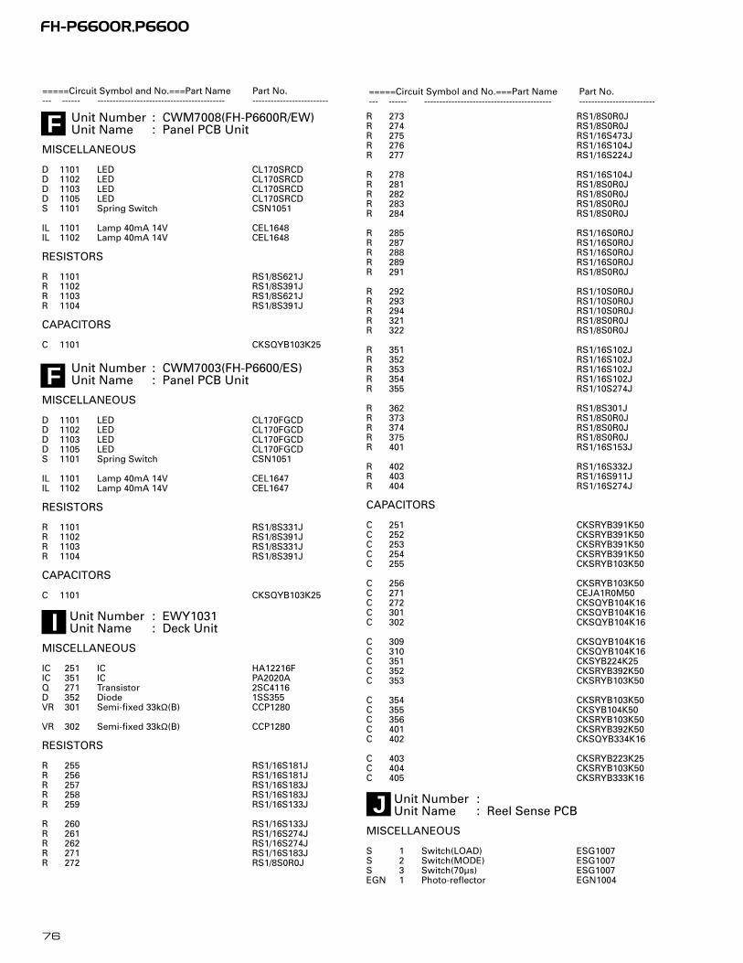
Unit Number : CWM7008(FH-P6600R/EW)Unit Name : Panel PCB Unit
MISCELLANEOUS
D 1101 LED CL170SRCDD 1102 LED CL170SRCDD 1103 LED CL170SRCDD 1105 LED CL170SRCDS 1101 Spring Switch CSN1051
IL 1101 Lamp 40mA 14V CEL1648IL 1102 Lamp 40mA 14V CEL1648
RESISTORS
R 1101 RS1/8S621JR 1102 RS1/8S391JR 1103 RS1/8S621JR 1104 RS1/8S391J
CAPACITORS
C 1101 CKSQYB103K25
Unit Number : CWM7003(FH-P6600/ES)Unit Name : Panel PCB Unit
MISCELLANEOUS
D 1101 LED CL170FGCDD 1102 LED CL170FGCDD 1103 LED CL170FGCDD 1105 LED CL170FGCDS 1101 Spring Switch CSN1051
IL 1101 Lamp 40mA 14V CEL1647IL 1102 Lamp 40mA 14V CEL1647
RESISTORS
R 1101 RS1/8S331JR 1102 RS1/8S391JR 1103 RS1/8S331JR 1104 RS1/8S391J
CAPACITORS
C 1101 CKSQYB103K25
Unit Number : EWY1031Unit Name : Deck Unit
MISCELLANEOUS
IC 251 IC HA12216FIC 351 IC PA2020AQ 271 Transistor 2SC4116D 352 Diode 1SS355VR 301 Semi-fixed 33kΩ(B) CCP1280
VR 302 Semi-fixed 33kΩ(B) CCP1280
RESISTORS
R 255 RS1/16S181JR 256 RS1/16S181JR 257 RS1/16S183JR 258 RS1/16S183JR 259 RS1/16S133J
R 260 RS1/16S133JR 261 RS1/16S274JR 262 RS1/16S274JR 271 RS1/16S183JR 272 RS1/8S0R0J
R 273 RS1/8S0R0JR 274 RS1/8S0R0JR 275 RS1/16S473JR 276 RS1/16S104JR 277 RS1/16S224J
R 278 RS1/16S104JR 281 RS1/8S0R0JR 282 RS1/8S0R0JR 283 RS1/8S0R0JR 284 RS1/8S0R0J
R 285 RS1/16S0R0JR 287 RS1/16S0R0JR 288 RS1/16S0R0JR 289 RS1/16S0R0JR 291 RS1/8S0R0J
R 292 RS1/10S0R0JR 293 RS1/10S0R0JR 294 RS1/10S0R0JR 321 RS1/8S0R0JR 322 RS1/8S0R0J
R 351 RS1/16S102JR 352 RS1/16S102JR 353 RS1/16S102JR 354 RS1/16S102JR 355 RS1/10S274J
R 362 RS1/8S301JR 373 RS1/8S0R0JR 374 RS1/8S0R0JR 375 RS1/8S0R0JR 401 RS1/16S153J
R 402 RS1/16S332JR 403 RS1/16S911JR 404 RS1/16S274J
CAPACITORS
C 251 CKSRYB391K50C 252 CKSRYB391K50C 253 CKSRYB391K50C 254 CKSRYB391K50C 255 CKSRYB103K50
C 256 CKSRYB103K50C 271 CEJA1R0M50C 272 CKSQYB104K16C 301 CKSQYB104K16C 302 CKSQYB104K16
C 309 CKSQYB104K16C 310 CKSQYB104K16C 351 CKSYB224K25C 352 CKSRYB392K50C 353 CKSRYB103K50
C 354 CKSRYB103K50C 355 CKSYB104K50C 356 CKSRYB103K50C 401 CKSRYB392K50C 402 CKSQYB334K16
C 403 CKSRYB223K25C 404 CKSRYB103K50C 405 CKSRYB333K16
Unit Number :Unit Name : Reel Sense PCB
MISCELLANEOUS
S 1 Switch(LOAD) ESG1007S 2 Switch(MODE) ESG1007S 3 Switch(70µs) ESG1007EGN 1 Photo-reflector EGN1004
76
FH-P6600R,P6600
J
I
F
=====Circuit Symbol and No.===Part Name Part No.--- ------ ------------------------------------------ -------------------------
=====Circuit Symbol and No.===Part Name Part No.--- ------ ------------------------------------------ -------------------------
F

Unit Number : CWX2434Unit Name : Control Unit(S8TX)
MISCELLANEOUS
IC 201 IC UPD63711GCIC 301 IC BA5985FMIC 701 IC BA05SFPQ 101 Transistor 2SB1132D 801 Chip LED CL200IRX
D 802 Chip LED CL200IRXS 801 Spring Switch(HOME) CSN1051S 802 Spring Switch(CLAMP) CSN1052
RESISTORS
R 101 RS1/8S120JR 102 RS1/8S100JR 103 RS1/16S222JR 201 RS1/16S104JR 202 RS1/16S103J
R 203 RS1/16S393JR 204 RS1/16S103JR 205 RS1/16S103JR 206 RS1/16S182JR 207 RS1/16S123J
R 211 RS1/16S0R0JR 212 RS1/16S272JR 302 RS1/16S153JR 303 RS1/16S103JR 501 RS1/16S102J
R 502 RA4C681JR 503 RS1/16S221JR 504 RS1/16S221JR 505 RS1/16S221JR 801 RS1/8S751J
R 803 RS1/8S751JR 901 RS1/16S681JR 903 RS1/16S0R0JR 904 RS1/16S681JR 905 RS1/16S681J
CAPACITORS
C 101 CKSRYB102K50C 102 CKSRYB104K16C 103 CEV101M6R3C 104 CEV470M6R3C 105 CKSQYB334K16
C 106 CKSQYB334K16C 107 CKSQYB334K16C 201 CKSRYB104K16C 202 CKSRYB471K50C 203 CKSRYB104K16
C 205 CEV101M6R3C 206 CKSRYB104K16C 207 CKSRYB104K16C 208 CKSRYB104K16C 209 CKSRYB104K16
C 210 CKSRYB332K50C 211 CKSRYB104K16C 212 CKSRYB104K16C 213 CKSRYB392K50C 214 CKSRYB104K16
C 215 CKSRYB104K16C 216 CCSRCJ3R0C50C 217 CCSRCH270J50C 218 CKSRYB104K16C 219 CCSRCH181J50
C 220 CCSRCH510J50C 221 CKSRYB682K25C 223 CCSRCH221J50C 301 CEV101M10C 702 10µF/10V CCH1349
C 703 CKSQYB334K16
Unit Number :Unit Name : Photo Unit(S8)
Q 1 Photo-transistor CPT230SX-TUQ 2 Photo-transistor CPT230SX-TU
Miscellaneous Parts List
Pickup Unit(Service)(P8) CXX1285M 1 Motor Unit(CARRIAGE) CXB5827M 2 Motor Unit(LOADING) CXB5828M 3 Motor Unit(SPINDLE) CXB5829M 1 Motor Unit(MAIN) EXA1490
M 2 Motor Unit(SUB) EXA1580HD 1 Head Assy EXA1589
77
FH-P6600R,P6600
G
H
=====Circuit Symbol and No.===Part Name Part No.--- ------ ------------------------------------------ -------------------------
=====Circuit Symbol and No.===Part Name Part No.--- ------ ------------------------------------------ -------------------------
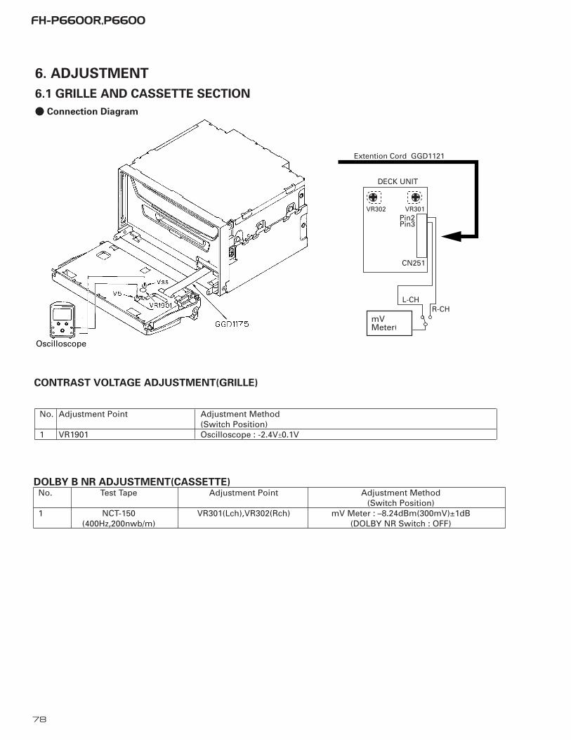
78
FH-P6600R,P6600
6. ADJUSTMENT
6.1 GRILLE AND CASSETTE SECTION
- Connection Diagram
CONTRAST VOLTAGE ADJUSTMENT(GRILLE)
No. Adjustment Point Adjustment Method(Switch Position)
1 VR1901 Oscilloscope : -2.4V±0.1V
VR302
mVMeter(2)
VR301
L-CHR-CH
Pin2Pin3
CN251
DECK UNIT
Extention Cord GGD1121
DOLBY B NR ADJUSTMENT(CASSETTE)No. Test Tape Adjustment Point Adjustment Method
(Switch Position)1 NCT-150 VR301(Lch),VR302(Rch) mV Meter : –8.24dBm(300mV)±1dB
(400Hz,200nwb/m) (DOLBY NR Switch : OFF)
Oscilloscope

79
FH-P6600R,P6600
1) Precautions• This unit uses a single power supply (+5V) for the
regulator. The signal reference potential, therefore, isconnected to REFO(approx. 2.5V) instead of GND.If REFO and GND are connected to each other bymistake during adjustments, not only will it beimpossible to measure the potential correctly, but theservo will malfunction and a severe shock will beapplied to the pick-up. To avoid this, take special noteof the following.Do not connect the negative probe of the measuringequipment to REFO and GND together. It is especiallyimportant not to connect the channel 1 negativeprobe of the oscilloscope to REFO with the channel 2negative probe connected to GND.Since the frame of the measuring instrument isusually at the same potential as the negative probe,change the frame of the measuring instrument tofloating status.If by accident REFO comes in contact with GND,immediately switch the regulator or power OFF.
• Always make sure the regulator is OFF whenconnecting and disconnecting the various filters andwiring required for measurements.
• Before proceeding to further adjustments andmeasurements after switching regulator ON, let theplayer run for about one minute to allow the circuitsto stabilize.
• Since the protective systems in the unit's software arerendered inoperative in test mode, be very careful toavoid mechanical and /or electrical shocks to thesystem when making adjustment.
• Disc detection during loading and eject operations isperformed by means of a photo transistor in thisunit.Consequently, if the inside of the unit is exposedto a strong light source when the outer casing isremoved for repairs or adjustment, the followingmalfunctions may occur.
*During PLAY, even if the eject button ispressed,the disc will not be ejected and the unitwill remain in the PLAY mode.
*The unit will not load a disc.When the unit malfunctions this way, either re-position the light source, move the unit or cover thephoto transistor.
2) Test ModeThis mode is used for adjusting the CD mechanismmodule of the device.
• Test mode starting procedureReset while pressing the 4 and 6 keys together.
• Test mode cancellationSwitch ACC, back-up OFF.
• After pressing the EJECT key, do not press any otherkey until the disk is completely ejected.
• If the ] or [ key is pressed while focus search is inprogress, immediately turn the power off (otherwisethe actuator may be damaged due to adhesion of thelenses).
• Jump operation of TRs other than 100TR continuesafter releasing the key. CRG move and 100TR jumpoperations are brought into the “Tracking close”status when the key is released.
• Powering Off/On resets the jump mode to “Single TR(91)”, the RF AMP gain setting to 0 dB, and theautomatic adjustment value to the initial value.
6.2 CD ADJUSTMENT

80
FH-P6600R,P6600
- Flow Chart
Focus Close*2 S Curve Check01 01 0100 00 00
(99 99 99)Display
TYP
4
3
Acc on
SOURCE
New test mode
[
BAND
BAND
BAND
BAND
BAND
3
*2
*1 +6dB +12dB
*4
*5
6
6
6
6
1
2
1
2]
] [
06 06 06 12 12 12
Sourse CD
Single TR 32TRK92(82)
CRG Move94(84)
100TRK93(83)
Focus ModeSelect
Focus Close/S Curve Check
CRG- Auto AdjustmentDisplay Select
<Tracking Servo Close> CRG+
RF AGC Coefficient Display/Rough Servo and RF AGC
Tracking Open
Display
TrackingOpen
T. Close andFit Servo
*3 F.Offset Display RF.Offset Display F.Cansel Display
*7
Single TR/32TR/100TR
Voltage of CRG Motor = 2 [V]
(F,T.AGC Gain = (Present Value/Initial Value) x 20)
*6
] [
1
3
Display
2
3
Displayor
8x 8x 8xTRK SECMIN
9x 9x 9xTRK SECMIN
or
CRG-CRG+ T.BalanceAdjustment
*7F, T, RF AGC/F.Bias Display Select
F, T AGC andRF AGC
CRG Move, 100TR Jump Only
TRK, MIN, SEC F.AGC Gain RF AGC GainT.AGC Gain
*8
Power ON(Adjustment for T.Offset)
*5 *4 *4
*6CRG/TR Jump NO.Select
CRG+/TR Jump+
CRG-/TR Jump-
Power OFF
Display
Display
Display
T.Close andF,T AGC andRF AGC andFit Servo
Display
Power ON(Not adjustment for T.Offset)
Display
Display
2
RF AMP Gain Select
2
Power OFF
Power OFF
Power OFF 8x 8x 8xTRK SECMIN
9x 9x 9xTRK SECMIN
8x 8x 8xTRK SECMIN
9x 9x 9xTRK SECMIN
or
8x 8x 8xTRK SECMIN
9x 9x 9xTRK SECMIN
or
00 00 00TRK SECMIN
99 99 99TRK SECMIN
or
00 00 00TRK SECMIN
99 99 99TRK SECMIN
or
00 00 00TRK SECMIN
99 99 99TRK SECMIN
or
91 91 91TRK SECMIN
0x 0x 0xTRK SECMIN
00 00 00TRK SECMIN
99 99 99TRK SECMIN
GG GG GGTRK SECMIN
Test Mode In
*1
*8 *3*8
F.Cancel Value = Top Rank 8bit of Set Value (7F [H] to 80 [H] ) + 128 / 4 = 63 [D] to (32 [D] ) to 00 [D]
9x(8x):91(81)
6

81
FH-P6600R,P6600
• Note :The grating angle of the PU unit cannot be adjusted after the PU unit is changed. The PU unit in the CDmechanism module is adjusted on the production line to match the CD mechanism module and is thus the bestadjusted PU unit for the CD mechanism module. Changing the PU unit is thus best considered as a last resort.However, if the PU unit must be changed, the grating should be checked using the procedure below.
• Purpose :To check that the grating is within an acceptable range when the PU unit is changed.
• Symptoms of Mal-adjustment :If the grating is off by a large amount symptoms such as being unable to close tracking, being unable to performtrack search operations, or taking a long time for track searching.
• Method :
• Measuring Equipment • Oscilloscope, Two L.P.F.• Measuring Points • E, F, REFO• Disc • ABEX TCD-784• Mode • TEST MODE
• Checking Procedure1. In test mode, load the disc and switch the 5V regulator on.2. Using the ] and [ buttons, move the PU unit to the innermost track.3. Press key 3 to close focus, the display should read "91". Press key 2 to implement the tracking balance
adjustment the display should now read "81". Press key 3 2 times. The display will change, returning to "81" onthe fourth press.
4. As shown in the diagram above, monitor the LPF outputs using the oscilloscope and check that the phasedifference is within 75° . Refer to the photographs supplied to determine the phase angle.
5. If the phase difference is determined to be greater than 75° try changing the PU unit to see if there is anyimprovement. If, after trying this a number of times, the grating angle does not become less than 75° then themechanism should be judged to be at fault.
• NoteBecause of eccentricity in the disc and a slight misalignment of the clamping center the grating waveform may beseen to "wobble" ( the phase difference changes as the disc rotates). The angle specified above indicates theaverage angle.
• HintReloading the disc changes the clamp position and may decrease the "wobble".
F
REFO
E
100kΩ
390pF
100kΩ
390pF
E
REFO
F
REFO
L.P.F.
L.P.F.
CONTROL UNIT
Xch Ych
Oscilloscope
6.3 CHECKING THE GRATING AFTER CHANGING THE PICKUP UNIT

82
FH-P6600R,P6600
Grating waveform Ech → Xch 20mV/div, ACFch → Ych 20mV/div, AC
45°
0°
75°
60°
30°
90°

83
FH-P6600R,P6600
7. GENERAL INFORMATION
7.1 DIAGNOSIS
7.1.1 TEST MODE
- Error Messages
If a CD is not operative or stopped during operation due to an error, the error mode is turned on and cause(s) of the
error is indicated with a corresponding number. This arrangement is intended at reducing nonsense calls from the
users and also for facilitating trouble analysis and repair work in servicing.
(1) Basic Indication Method
1) When SERRORM is selected for the CSMOD (CD mode area for the system), error codes are written to DMIN
(minutes display area) and DSEC (seconds display area). The same data is written to DMIN and DSEC. DTNO
remains in blank as before.
2) Main unit display examples
Depending on display capability of LCD used, display will vary as shown below. xx contains the error number.
8-digit display 6-digit display 4-digit display
ERROR–xx ERR–xx E–xx
OR
Err–xx
(2) Error Code List
Code Class Displayed error code Description of the code and potential cause(s)
10 Electricity Carriage Home NG CRG can't be moved to inner diameter.
CRG can't be moved from inner diameter.
→ Failure on home switch or CRG move mechanism.
11 Electricity Focus Servo NG Focusing not available.
→ Stains on rear side of disc or excessive vibrations on REWRITABLE.
12 Electricity Spindle Lock NG Spindle not locked. Sub-code is strange (not readable).
→ Failure on spindle, stains or damages on disc, or excessive vibrations.
Subcode NG A disc not containing CD-R data is found. Turned over disc are found,
though rarely.
→ Failure on home switch or CRG move mechanism.
RF AMP NG An appropriate RF AMP gain can't be determined.
→ CD signal error.
17 Electricity Setup NG APC protection doesn't work. Focus can be easily lost.
→ Damages or stains on disc, or excessive vibrations.
30 Electricity Search Time Out Failed to reach target address.
→ CRG tracking error or damages on disc.
A0 System Power Supply NG Power (VD) is ground faulted.
→ Failure on SW transistor or power supply (failure on connector).
Remarks: Mechanical errors are not displayed (because a CD is turned off in these errors).
Unreadable TOC does not constitute an error. An intended operation continues in this case.
A newly designed main unit must conform to the example given above.
Upper digits of an error code are subdivided as shown below:
1x: Setup relevant errors, 3x: Search relevant errors, 3x: Search relevant errors, Ax: Other errors.
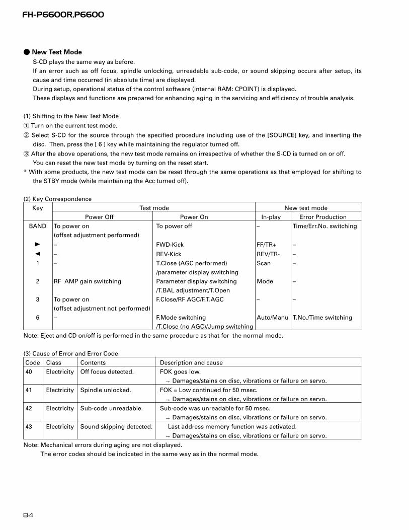
84
FH-P6600R,P6600
- New Test Mode
S-CD plays the same way as before.
If an error such as off focus, spindle unlocking, unreadable sub-code, or sound skipping occurs after setup, its
cause and time occurred (in absolute time) are displayed.
During setup, operational status of the control software (internal RAM: CPOINT) is displayed.
These displays and functions are prepared for enhancing aging in the servicing and efficiency of trouble analysis.
(1) Shifting to the New Test Mode
1 Turn on the current test mode.
2 Select S-CD for the source through the specified procedure including use of the [SOURCE] key, and inserting the
disc. Then, press the [ 6 ] key while maintaining the regulator turned off.
3 After the above operations, the new test mode remains on irrespective of whether the S-CD is turned on or off.
You can reset the new test mode by turning on the reset start.
* With some products, the new test mode can be reset through the same operations as that employed for shifting to
the STBY mode (while maintaining the Acc turned off).
(2) Key Correspondence
Key Test mode New test mode
Power Off Power On In-play Error Production
BAND To power on To power off – Time/Err.No. switching
(offset adjustment performed)
] – FWD-Kick FF/TR+ –
[ – REV-Kick REV/TR- –
1 – T.Close (AGC performed) Scan –
/parameter display switching
2 RF AMP gain switching Parameter display switching Mode –
/T.BAL adjustment/T.Open
3 To power on F.Close/RF AGC/F.T.AGC – –
(offset adjustment not performed)
6 – F.Mode switching Auto/Manu T.No./Time switching
/T.Close (no AGC)/Jump switching
Note: Eject and CD on/off is performed in the same procedure as that for the normal mode.
(3) Cause of Error and Error Code
Code Class Contents Description and cause
40 Electricity Off focus detected. FOK goes low.
→ Damages/stains on disc, vibrations or failure on servo.
41 Electricity Spindle unlocked. FOK = Low continued for 50 msec.
→ Damages/stains on disc, vibrations or failure on servo.
42 Electricity Sub-code unreadable. Sub-code was unreadable for 50 msec.
→ Damages/stains on disc, vibrations or failure on servo.
43 Electricity Sound skipping detected. Last address memory function was activated.
→ Damages/stains on disc, vibrations or failure on servo.
Note: Mechanical errors during aging are not displayed.
The error codes should be indicated in the same way as in the normal mode.

85
FH-P6600R,P6600
(4) Display of Operational Status (CPOINT) during SetupStatus No. Contents Protective action00 CD+5V ON process in progress. None01 Servo LSI initialization (1/3) in progress. None02 Servo LSI CRAM initialization in progress. None03 Servo LSI initialization (2/3) in progress. None04 Offset adjustment (1/3) in progress. None05 Offset adjustment (2/3) in progress. None06 Offset adjustment (3/3) in progress. None07 FZD adjustment in progress. None08 Servo LSI initialization (3/3) in progress. None10 Carriage move to home position started. None11 Carriage move to home position started. None12 Carriage is moving toward inner diameter. Specified 10 seconds has been passed or failure
on home switch.13 Carriage is moving toward outer diameter. Specified 10 seconds has been passed or failure
on home switch.14 Carriage outer kick in progress. None15 Carriage outer diameter feed (1 second) in progress. None20 Servo close started. None21 Pre-processing for focus search started. None22 Spindle rotation and focus search started. None23 Waiting for focus close (XSI=Low). Specified focus search time has been passed.24 Standing by after focus close is over. Specified focus search time has been passed.25 Focus search preprocessing is in None
progress while setup protection is turned on.26 Focus search preprocessing is in None
progress while focus recovery is turned on.27 Wait time after focus close is set up. Off focus.28 Standing by after focus close is over. Off focus.29 Setup (1/2) before T balance adjustment is started. Off focus.30 Setup (2/2) before T balance adjustment is started. Off focus.31 T balance adjustment started. Off focus.32 T balance adjustment (1/2). Off focus.33 T balance adjustment (2/2). Off focus.34 Waiting for spindle rotation to end. Off focus.
Spindle rough servo.35 Standing by after spindle rough servo is over. Off focus.36 RF AGC started. Off focus.37 RF AGC started. Off focus.38 RF AGC ending process in progress. Off focus.39 Tracking close in progress. Off focus.40 Standing by after tracking is closed. Off focus.
Carriage closing in progress.41 Focus/tracking AGC started. Off focus.42 Focus AGC started. Off focus.43 Focus AGC in progress. Off focus.44 Tracking AGC in progress. Off focus.45 Standing by after focus/tracking AGC are over. Off focus.46 Spindle processes applicable servo. Off focus.47 Check for servo close is started. Off focus.48 Check of LOCK pin started. Off focus or spindle not locked.49 RF AGC started. Off focus.50 RF AGC in progress. Off focus.51 Standing by after RF AGC is over. Off focus.

86
FH-P6600R,P6600
(5) Display Examples
1) During Setup (When status no. = 11)
TRK No. MIN. SEC.
11 11' 11"
2) During Operation (TOC read, TRK search, Play, FF and REV)
The same as in the normal mode.
3) When a Protection Error Occurred
Switch to the following displays (A) and (B) using the [BAND] switch:
(A) Error occurrence timing display in absolute time.
An example: Error occurred in 12th tune at 34'56" in absolute time.
TRK No. MIN. SEC.
12 34' 56"
(B) Error No. display
An example: Error #40 (Off focus is detected)
ERROR-40
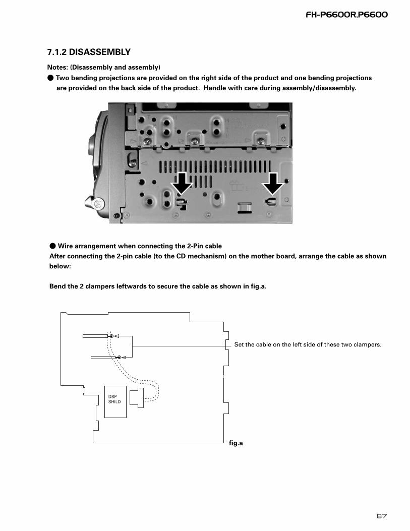
87
FH-P6600R,P6600
7.1.2 DISASSEMBLY
Notes: (Disassembly and assembly)
- Two bending projections are provided on the right side of the product and one bending projections
are provided on the back side of the product. Handle with care during assembly/disassembly.
- Wire arrangement when connecting the 2-Pin cable
After connecting the 2-pin cable (to the CD mechanism) on the mother board, arrange the cable as shown
below:
Bend the 2 clampers leftwards to secure the cable as shown in fig.a.
DSPSHILD
Set the cable on the left side of these two clampers.
fig.a

88
FH-P6600R,P6600
- Correctly set the folded FFC, located on the 2nd-floor chassis under the CD mech, as shown in fig. b.
Prevent the folded part of the FFC from coming into the chassis center hole for the SPDL motor.
HE
AT
SIN
K
FFCFFC
Fig. c : NG.
The FFC is positioned properly so that the
stretched part passes over the hole.
Fig.1
CD Mechanism Module
- Removing the Upper Case (not shown)
Remove the upper case.
- Removing the CD Mechanism Module (Fig.1)
Remove the four screws.
Disconnect the connector and then remove the CD
Mechanism Module.
Fig. b: OK.
HE
AT
SIN
K

89
FH-P6600R,P6600
Heat Sink- Removing the Heat Sink (Fig.4)
Remove the two screws.
Remove the two screws.
Remove the two screws and then remove
the Heat Sink.
Fig.4
Slit
- Removing the Grille Unit (Fig.2 and Fig.3)
Use a pair of tweezers or something like that. Insert
the tips into the bottom panel slits and slide the rail
in the direction indicated by an arrow in Fig.2 until
the grille moves down to the bottom.(Fig.2)
Remove the screw. (Fig.3)
Remove the screw. (Fig.3)
Remove the screw. (Fig.3)
Note: In the other side, remove the fixing three
screws in the same manner as above. Then, you
can remove the Grille Unit.
Fig.2 Fig.3
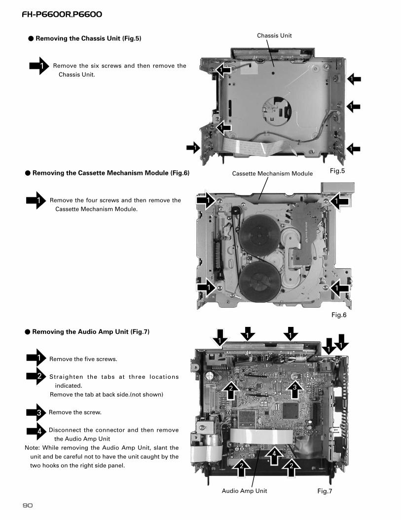
90
FH-P6600R,P6600
Chassis Unit
Cassette Mechanism Module
Audio Amp Unit
- Removing the Chassis Unit (Fig.5)
Remove the six screws and then remove the
Chassis Unit.
- Removing the Cassette Mechanism Module (Fig.6)
Remove the four screws and then remove the
Cassette Mechanism Module.
Fig.5
Fig.6
Fig.7
- Removing the Audio Amp Unit (Fig.7)
Remove the five screws.
Straighten the tabs at three locations
indicated.
Remove the tab at back side.(not shown)
Remove the screw.
Disconnect the connector and then remove
the Audio Amp Unit
Note: While removing the Audio Amp Unit, slant the
unit and be careful not to have the unit caught by the
two hooks on the right side panel.

91
FH-P6600R,P6600
- Removing the Upper Frame
1. Remove six Springs A, two Springs B and four
Screws.
2. Remove two Tabs situated on rear side of the Upper
Frame, remove two Arms on the front side, then
remove two Tabs on the front side.
- Removing the Carriage Mechanism Section
1. Disengage the Carriage Mechanism Section from the
two dampers situated in the front side by driving it
up, then disengage and remove the mechanism from
the one damper by driving it up aslant into front side
direction.
Note : When assembling the Carriage Mechanism
Section, coat the dampers with alcohol prior
to the assembly.
- Removing the Clamp Arm Assy Section
1. Remove a Spring A, a B and a Spring C.
2. Drive the Clamp Arm Assy Section up into rear side
direction, then disengage the arm from its current
position Finally, drive the assembly approximately 45
degrees upward, then slide the assembly toward
right side to remove it.
B
A
B A
A
A
Arm
Arm
Upper Frame
A
A
A
B
C
Carriage Mechanism Section
Clamp Arm Assy Section

92
FH-P6600R,P6600
- Removing the Guide Arm Assy Section
1. Remove a connector, a spring A and B
2. Drive the Guide Arm Assy Section up aslant into rear
side direction, then remove it from a Pin. Finally, drive
the assembly approximately 45 degrees upward, then
slide the assembly toward left side to remove it.
Note : When assembling the Guide Arm Assy Section,
route the cord inside the assembly. In this
operation, care must be exercised so that cord may
be caught by the gear.
- Removing the LO Arm Assy Section
1. Remove two Pins to dismount the LO Arm Assy
Section.
- Removing the Control Unit and the Spindle
Motor
1. Remove from the connector after mounting the short
pin on the flexible PCB of the pickup unit.
2. Remove two Soldered joints, then remove two Screws
A.
3. Remove two connectors and a Screw B.
4. Disengage the Control Unit from two Tabs, then
dismount the unit by sliding it toward left.
5. Dismount the Spindle Motor.
A
Guide Arm Assy Section
B
Pin
LO Arm Assy Section
Spindle Motor
A A
Control Unit
Short Pin
B

93
FH-P6600R,P6600
- Removing the Loading Motor and Carriage
Motor
1. Remove the Spring and two Screws A.
2. Dismount the Loading Motor.
3. Remove the Belt, a Screw B, two Screws C, a Guide
and a Screw Unit.
4. Dismount the Carriage Motor.
Note : When assembling the Belt, use care so that it may
not be contaminated by grease.
- Removing the Pickup Unit
1. Remove two Screws and a Shaft.
2. Dismount the Pickup Unit.
Pickup Unit
Shaft
CGuide
B
Screw Unit Carriage Motor
AA
CBelt
Loading Motor

94
FH-P6600R,P6600
7.1.3 PCB LOCATIONS
PANEL PCBUNIT
LED PCB
FLAP PCB
CONTROL UNIT
PHOTO UNIT
AUDIO AMP UNIT
DECK UNIT
FM/AM TUNERUNIT
POWER SUPPLY UNIT
H
C
E
F
D
G
J
B
A
REEL SENSE PCB
I

95
FH-P6600R,P6600
36
3772
73
108
109
144
1
*PE5124A(FH-P6600R/EW),*PE5122A(FH-P6600/ES)
7.2 PARTS
7.2.1 IC
*PM0017AM
PM0017AM
PE5124A(FH-P6600R/EW)
PE5122A(FH-P6600/ES)
PDG255A
HA12216F
PE5149A
BA033T
SED1526F0A
UPD63711GC
M62361FP
PQ20RX1S-L
1 2 3 4
24 23 22 21
A G
ND
VR
EF
IN1
IN2
AV
CC
5 6 7 8
20 19 18 17
IN3
IN4
IN5
IN6
9 10 11 12
16 15 14 13
NC
NC
CT
D G
ND
NC
DV
CC
OU
T1
OU
T2
OU
T3
OU
T4
OU
T5
OU
T6
DA
TA
CLK
ST
B
IC's marked by* are MOS type.
Be careful in handling them because they are very
liable to be damaged by electrostatic induction.

96
FH-P6600R,P6600
- Pin Functions (PE5124A,PE5122A)Pin No. Pin Name I/O Function and Operation
1 st I Stereo input2 SD I SD input 3 RECIVE O During RDS data reception output4 LOCH O LOC H output5 LOCL O LOC L output6 antfix O Tuner diversity fix select output7 AM/fm O AM/FM select output8 tmute O Tuner mute output9 RESET I Reset Input
10 X2 Crystal oscillator connection pin11 X1 Crystal oscillator connection pin12 VSS GND13 RSGC1 Regulator output connect14 VDD0 Power supply15 REGC0 Regulator output connect16 VSS0 GND17 XT2 Not used18 XT1 Not used19 CKSEL I Master clock frequency select input20 drst O Reset output21 rdslk I RDS LK signal input22 RDT I RDS data input23 NL2DT I RDS noise level input24 currq O Tuner voltage FIX output25 CD5VON O CD +5V power supply control output26 BKLT O Back light illumination output27 DIMMER O DIMMER select output28 VPP ROM write power supply29 SOR0 O Source select output30 SOR1 O Source select output31 SOR2 O Source select output32 SOR3 O Source select output33 VST O Strobe pulse output for electronic volume34 VCK O Clock output for electronic volume35 VDT O Data output for electronic volume36 FLAPILM O Flap illumination output37 DADT O DA data output (TV tuner screen control)38 DACK O DA clock output (TV tuner screen control)39 DAST O DA strobe output (TV tuner screen control)40 XA0 O Control signal distinguishing data from microcomputer41 DSPRST O DSP reset control42 MCKOUT O MCK gate control output43 DSPCD O DSP address output44 DSPRDY I Microcomputer I/F reception enable output45 ROMCS O ROM correction chip select output46 ROMCLK O ROM correction clock output47 ROMDATA O ROM correction data output48 bsrq I P-BUS service request input pin49 brxen I/O P-BUS reception enable input/output50 brst O P-BUS reset input51 LOCK I Spindle lock detector input52 FOK I FOK signal input53 MIRR I MIRR detection signal input terminal54 CLAMP I Disc clamp sense input55 CONT O Servo driver power supply control56 VDCONT O VD control output57 CDMUTE O CD mute output58 CDEJECT O Load motor eject output

97
FH-P6600R,P6600
Pin No. Pin Name I/O Function and Operation59 CDLOAD O Load motor loading control output60 xstb O CD LSI strobe output61 VSS2 GND62 VDD1 Device power supply terminal63 PLAY O MS gain select output64 NR O Dolby NR ON/OFF select output65 SC1 O Cassette mechanism sub motor control output66 SC2 O Cassette mechanism sub motor control output67 CM O Cassette mechanism capstan motor control output68 MSIN I MS sense69 DIRO O Head F/R select output70 MTLSW I Metal sense input71 LOADSW I Tape loading input72 POS I Cassette mechanism position sense input73 RES I Cassette mechanism reverse end sense input74 NES I Cassette mechanism forward end sense input75 STBY O Stand-by output terminal76 RIMUTE O R.I. mute output77 ILMPW O Illumination power supply control output78 ANTPW O Antenna output79 MUTE O System mute output80 SYSPW O System power supply control output81 DALMON O DFS alarm output82 fopnsw I FLAP open sense SW input83 folssw I FLAP close sense SW input84 FALP0 O FLAP motor driver control output85 FLAP1 O FLAP motor driver control output86 FLAPPW O FLAP motor driver power supply control output87 ASENBO O Slave power supply control output88 IPPW O IP-BUS driver power supply control output89 TX O Digital audio interface data output terminal90 RX I IP-BUS data input91 SUBOK O MD service request output92 RECMUTE O MD recording mute output93 TSTB O CDTEXT strobe output94 SHELL I Cassette shell input95 xrst O CD LSI reset output96 bsens I Back up power sense input97 asens I ACC power sense input98 isens I Illumination sense input99 PACK I CDTEXT pack synchroning signal input
100 RCK I FROM clock input101 ldet I PLL lock sense input102 NC Not used103 AVDD Positive power supply terminal for analog circuit104 AVSS A/D GND105 AVREF A/D converter reference voltage106 SL I SD level input from tuner107 NL I Noise level input108 SDBW I SDBW input109 MODEL I Model select input110 EJTSNS I Disc EJECT position detect111 DSCSNES I DISC insertion sense input112 VDSENS I Over voltage sense input113 TEMP I Temperature detector input114 flapejsw I FLAP CD EJECT position sense input115 FLSEN0 I FLAP position sense input116 FLSEN1 I FLAP position sense input

98
FH-P6600R,P6600
Pin No. Pin Name I/O Function and Operation117 TELIN I Telephone mute input118 TESTIN I Test program mode input119 XSI I LSI data input120 XSO O LSI data output121 XSCK O LSI clock output122 TSI I Test program serial input 123 TSO O Test program serial output124 TSCK O Test program clock output125 TUNPCE2 O PLL IC chip enable126 TUNPCE O PLL IC chip enable127 TUNPDI I PLL IC data input128 TUNPDO O PLL IC data output129 TUNPCK O PLL IC clock130 PCL O Clock adjustment output131 DSPMS DSP slave/master select132 BSI I P-BUS serial data input133 BSO O ALPINE-BUS output 134 BSCK O P-BUS clock output135 VSS3 GND136 VDD2 Device power supply terminal137 SWVDD O Grille power supply control output138 DPDT O Display data output139 KEYDT I Display data input140 DSPCK O DSP serial clock output141 DSPOUT O DSP serial data output142 DSPIN I DSP serial data input143 RDS57K I 57kHzBP-OUT sense input144 PEE O Beep tone output
PLCLK
XECKSTP
AVDP
VSS4
T.P
T.P
T.P
T.P
T.P
T.P
T.P
T.P
T.P
T.P
VDD4
AVSD
T.P
T.P
T.P
AVDD
AVS6
AVD2
AVS2
RREF
RIN
AVS8
AVD8
AOUTR2
AVSX
XTLI38
XTLO38
AVDX
AOUTL2
AVD7
AVS7
LIN
LREF
AVS1
AVD1
AVS5
80
81
82
83
84
85
86
87
88
89
90
91
92
93
94
95
96
97
98
99
100
79 7778 76 7475 73 7172 70 6869 67 6566 64 6263 5657 55 53 52 515461 5960 58
50
49
48
47
46
45
44
43
42
41
40
39
38
37
36
35
34
33
32
31
1 2 43 5 76 8 109 11 1312 14 1615 17 1918 2524 26 28 29 302720 2221 23
XP
LL
EN
AV
SP
VD
D3
XM
ST
LR
CK
BC
K
SIN
SI3
SI2
SI1
SO
UT
SO
3
SO
2
SO
1
VS
S3
VD
D2
XS
24
RV
DT
XL
AT
TR
DT
RE
DY
SC
K
BF
OT
XR
ST
VS
S2
AV
S4
AO
UT
R3
AV
D4
AO
UT
L3
AV
D6
VS
S1
T.P
T.P
T.P
T.P
T.P
T.P
T.P
T.P
T.P
T.P
T.P
T.P
T.P
T.P
TS
T0
TS
T1
TS
T2
TS
T3
TS
T4
TS
T5
JPE
1
JPE
2
JPE
3
VD
D1
AV
S3
AO
UT
L1
AV
D3
AO
UT
R1
AV
D5
SERIAL DATA I/F
SERIAL DATAI/F
CLOCKGENERATOR
/TIMINGCIRCUIT
PLL
512K bitDELEY RAM
MICRO-COMPUTERI/F
ADC2DAC5 +
–
DAC4 +–
DAC4 +–
DAC3 +–
DAC2 +–
DAC1 +–
ADC1
DIGITALFILTER
DSP
CLOCKGENERATOR
/TIMINGCIRCUIT
*PDG255A
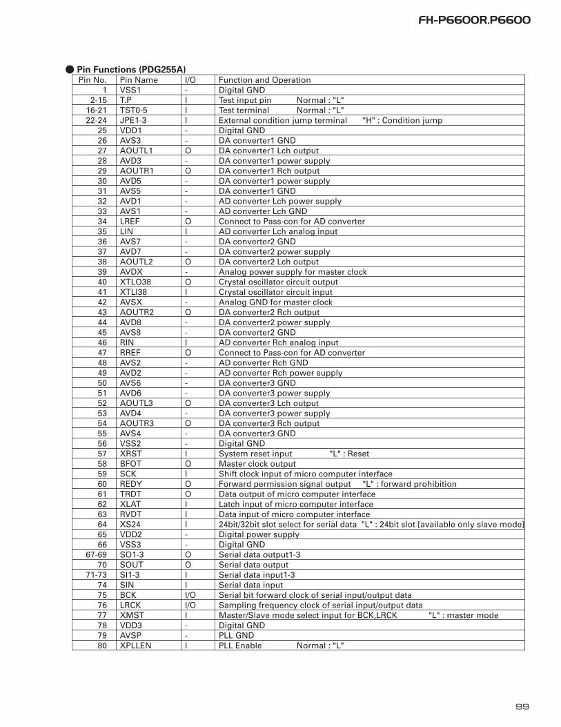
99
FH-P6600R,P6600
- Pin Functions (PDG255A)Pin No. Pin Name I/O Function and Operation
1 VSS1 - Digital GND2-15 T.P I Test input pin Normal : "L"
16-21 TST0-5 I Test terminal Normal : "L"22-24 JPE1-3 I External condition jump terminal "H" : Condition jump
25 VDD1 - Digital GND26 AVS3 - DA converter1 GND27 AOUTL1 O DA converter1 Lch output28 AVD3 - DA converter1 power supply29 AOUTR1 O DA converter1 Rch output30 AVD5 - DA converter1 power supply31 AVS5 - DA converter1 GND32 AVD1 - AD converter Lch power supply33 AVS1 - AD converter Lch GND34 LREF O Connect to Pass-con for AD converter35 LIN I AD converter Lch analog input36 AVS7 - DA converter2 GND37 AVD7 - DA converter2 power supply38 AOUTL2 O DA converter2 Lch output39 AVDX - Analog power supply for master clock40 XTLO38 O Crystal oscillator circuit output41 XTLI38 I Crystal oscillator circuit input42 AVSX - Analog GND for master clock43 AOUTR2 O DA converter2 Rch output44 AVD8 - DA converter2 power supply45 AVS8 - DA converter2 GND46 RIN I AD converter Rch analog input47 RREF O Connect to Pass-con for AD converter48 AVS2 - AD converter Rch GND49 AVD2 - AD converter Rch power supply50 AVS6 - DA converter3 GND51 AVD6 - DA converter3 power supply52 AOUTL3 O DA converter3 Lch output53 AVD4 - DA converter3 power supply54 AOUTR3 O DA converter3 Rch output55 AVS4 - DA converter3 GND56 VSS2 - Digital GND57 XRST I System reset input "L" : Reset58 BFOT O Master clock output59 SCK I Shift clock input of micro computer interface60 REDY O Forward permission signal output "L" : forward prohibition61 TRDT O Data output of micro computer interface62 XLAT I Latch input of micro computer interface63 RVDT I Data input of micro computer interface64 XS24 I 24bit/32bit slot select for serial data "L" : 24bit slot [available only slave mode]65 VDD2 - Digital power supply66 VSS3 - Digital GND
67-69 SO1-3 O Serial data output1-370 SOUT O Serial data output
71-73 SI1-3 I Serial data input1-374 SIN I Serial data input75 BCK I/O Serial bit forward clock of serial input/output data76 LRCK I/O Sampling frequency clock of serial input/output data77 XMST I Master/Slave mode select input for BCK,LRCK "L" : master mode78 VDD3 - Digital GND79 AVSP - PLL GND80 XPLLEN I PLL Enable Normal : "L"

100
FH-P6600R,P6600
Pin No. Pin Name I/O Function and Operation81 PLCLK O PLL clock output82 XECKSTP I PLL clock output control "L" : PLCLK output "L" "H" : PLL clock output83 AVDP - PLL power supply84 VSS4 - Digital GND
85-94 T.P I Test input pin Normal : "L"95 VDD4 - Digital power supply96 AVSD - DRAM GND
97-99 T.P I Test input pin Normal : "L"100 AVDD - DRAM power supply
31
32
33
34
35
36
37
38
39
40
1 2 3 4 5 6 7 8 9 10
11
12
13
14
15
16
17
18
19
20
21222324252627282930
MSGV(R)
MAOUT
MSI
MSDET
VCC
MSOUT
MSGV
F/R
120/70
NR
MO
UT
(L)
EQ
OU
T(L
)
TA
I(L)
NC
RA
I(L)
PB
OU
T(L
)
NC
DE
T(L
)
NC
MS
GV
(S)
NFI(L)
RIN(L)
RIP
FIN(L)
GND
GND
FIN(R)
VREF
RIN(R)
NFI(R)
M-O
UT
(R)
EQ
OU
T(R
)
TA
I(R
)
BIA
S
RA
I(R
)
PB
OU
T(R
)
NC
DE
T(L
)
NC
MU
TE
Dolby B-N
LPF
DETS/R
T/R
Dolby B-N
T/RF/R
F/R
HA12216F

101
FH-P6600R,P6600
- Pin Functions (PE5149A)Pin No. Pin Name I/O Format Function and Operation
1 avsw O AV switch output2,3 NC Not used
4 AVSS I A/D GND5,6 NC Not used
7 AVREF I A/D converter reference voltage8 DISPDIN I Display data input9 KEYDOUT O C Key data output
10–15 NC Not used16 TESTDIN I Test data input17 TESTDOUT O C Test data output18 TESTCLK Test data clock
19–26 SD0-7 I/O C Display driver command/Data input/output27–32 NC Not used
33 GND GND34–39 NC Not used
40 rd O C Read strobe41 wr O C Write strobe
42,43 NC Not used44 LCDCTRL O C Display driver control45 LCDRESET O C Display driver reset control
46–49 NC Not used50 ejectcd I CD eject key input51 ejectmdcc I MD/CC eject key input
52–59 NC Not used60 reset I Reset input61 remin I Key cord signal input62 TESTIN I Test program mode input63 ce Devise select input
64–67 NC Not used68 VDD Power supply69 X2 Crystal oscillator connection pin70 X1 Crystal oscillator connection pin
71–73 NC Not used74 AVDD Positive power supply terminal for analog circuit75 AVREF0 GND
76–80 KD0-4 I Key data input
20
21
40
41 60
61
80
1
*PE5149A
Reference voltage
+
Vcc GND OUT
1 2 3
VCC
BA033T

102
FH-P6600R,P6600
*SED1526F0A
- Pin Functions (SED1526F0A)Pin No. Pin Name I/O Function and Operation
1-5 V1-V5 Multilevel power supply for driving LCD6 VR I Voltage adjustment7 VDD +5V power supply8 VOUT O Ascending voltage output9 CAP2- O Ascending voltage capacitor connection
10 CAP2+ O Not used11 CAP1- O Ascending voltage capacitor connection12 CAP2+ O Ascending voltage capacitor connection13 VSS GND14 M/S I IC master/slave operation select15 SR2 I MPU interface select, pararel/serial data input select and reset input16 SR1 I MPU interface select, pararel/serial data input select and reset input17 wr I MPU WR signal connection18 rd I MPU RD signal connection19 CS2 I Chip select signal20 CS1 I Chip select signal21 A0 I Data/command discrimination22 FR O Not used23 CL O Not used
24-31 D0-D7 I/O Serial data bus32-39 COM0-7 O Output for LCD common driving40-48 NC Not used
49-128 SEG0-79 O Output for driving segment of LCD

103
FH-P6600R,P6600
- Pin Functions (UPD63711GC)Pin No. Pin Name I/O Function and Operation
1 D.GND Logic circuit GND2 RFOK O RFOK signal output3 rst I Reset signal input4 A0 I Command/parameter identification signal input5 stb I Data strobe signal input6 sck I Clock signal input for serial data input/output7 SO O Serial data and status signal output8 SI I Serial data input9 xtalen I Crystal oscillation control pin
10 D.VDD Positive power supply terminal to logic circuit11 DA.VDD Positive power supply terminal to D/A converter12 R_OUT O Right channel audio output signal13 DA.GND D/A converter GND14 REGC I The outside putting capacitor connection pin for SCF regulator15 DA.GND D/A converter GND16 L_OUT O Left channel audio output signal17 DA.VDD Positive power supply terminal to D/A converter18 R+ O Right channel audio data output19 R- O Right channel audio data output20 L- O Left channel audio data output21 L+ O Left channel audio data output22 X.VDD Positive power supply terminal to crystal oscillation circuit23 XTAL I Crystal oscillator connect pin24 xtal O Crystal oscillator connect pin25 X.GND Crystal oscillation circuit GND26 D.VDD Positive power supply terminal to logic circuit27 EMPH O Output pin for the pre-emphasis data in the sub-Q code28 FLAG O Flag output pin to indicate that audio data currently being output consists
of noncorrectable data29 DIN I Serial data input to internal DAC30 DOUT O Serial audio data output31 SCKIN I Serial clock input to internal DAC32 SCKO O Audio data that is output from DOUT changes at rising edge of this clock33 LRCKIN I LRCK signal input to internal DAC34 LRCK O Signals to distinguish the right and left channels of the audio data output
from DOUT35 HOLD O Defect detection output36 TX O Digital audio interface data output37 D.GND Logic circuit GND38 C16M O Oscillator clock buffering output39 LIMIT I Status of the pin is output at Bit 5 of the status output40 D.VDD Positive power supply terminal to logic circuit41 LOCK O EFM synchronous detection signal42 RFCK O Frame synchronous signal of XTAL-system43 MIRR O MIRR output44 PLCK O Monitor pin of bit clock45 D.GND Logic circuit GND46 C1D1 O Output pin for indicating the C1 error correction results47 C1D2 O Output pin for indicating the C1 error correction results48 C2D1 O Output pin for indicating the C2 error correction results49 C2D2 O Output pin for indicating the C2 error correction results50 C2D3 O Output pin for indicating the C2 error correction results51 D.VDD Positive power supply terminal to logic circuit52 PACK O CD-TEXT PACK synchronous signal53 TSO O CD-TEXT data serial output54 TSI I CD-TEXT control parameter serial input55 tsck I CD-TEXT serial clock input56 TSTB I CD-TEXT parameter strobe signal input57 D.GND Logic circuit GND

104
FH-P6600R,P6600
Pin No. Pin Name I/O Function and Operation58 TEST0 I Test pin59 TEST1 I Test pin60 ATEST O Test pin61 A.GND Analog circuit GND62 FD O Focus drive output63 TD O Tracking drive output64 SD O Sled drive output65 MD O Spindle drive output66 DAC0 O DAC output for adjustment67 DAC1 O DAC output for adjustment68 DAC2 O DAC output for adjustment69 DAC3 O DAC output for adjustment70 A.VDD Positive power supply terminal to analog circuit71 EFM O EFM signal output72 ASY I EFM comparator reference voltage input73 C3T 3T detection capacitor additional pin74 RFI I RF signal input for EFM data regulation75 AGCO O RF signal output of after gain adjustment 76 AGCI I RF-AGC amplifier input77 RFO O RF summing amplifier output78 EQ2 RF amplifier equalizer parts additional pin79 EQ1 RF amplifier equalizer parts additional pin80 RF- I RF summing amplifier inverted input81 A.GND Analog circuit GND82 A I Photo detector A input83 C I Photo detector C input84 B I Photo detector B input85 D I Photo detector D input86 F I Photo detector F input87 E I Photo detector E input88 A.VDD Positive power supply terminal to analog circuit89 REFOUT O Reference electric potential output90 FE- I Focus error amplifier inverted input91 FEO O Focus error amplifier output92 TE- I Tracking error amplifier inverted input93 TEO O Tracking error amplifier output94 TE2 O Tracking error output of after amplification95 TEC I Tracking comparator input96 A.GND Analog circuit GND97 PD I PD detection signal input for LD output monitor 98 LD O LD control current output99 PN I APC circuit control polarity set pin
100 A.VDD Positive power supply terminal to analog circuit
25
2650
51
75
76 100
1
*UPD63711GC
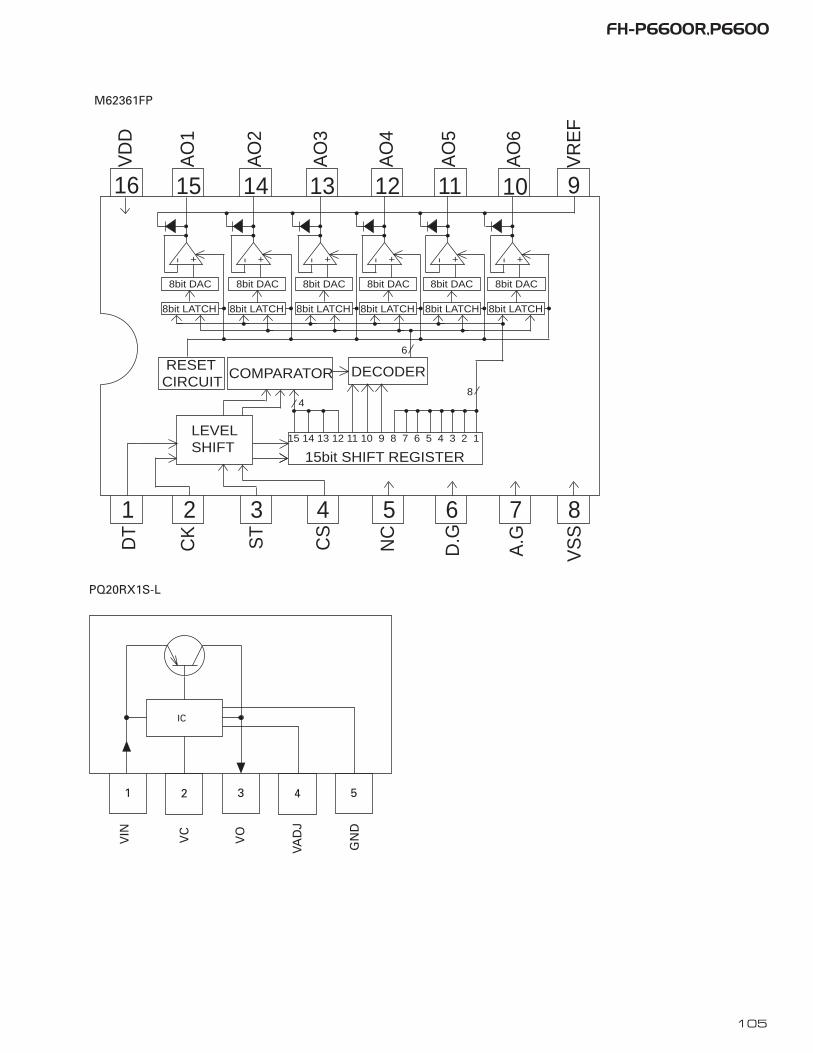
105
FH-P6600R,P6600
LEVELSHIFT
15bit SHIFT REGISTER15 14 13 12 11 10 9 8 7 6 5 4 3 2 1
COMPARATOR
48
DECODER
8bit LATCH
8bit DAC
+-
RESETCIRCUIT
6
8bit LATCH
8bit DAC
+-8bit LATCH
8bit DAC
+-
8bit LATCH
8bit DAC
+-
8bit LATCH
8bit DAC
+-
8bit LATCH
8bit DAC
+-
16 15 14 13 12 11 10 9
87654321
DT
CK ST
CS
NC
D.G
A.G
VS
S
VD
D
AO
1
AO
2
AO
3
AO
4
AO
5
AO
6
VR
EF
M62361FP
GN
D
VO
VC
IC
52 3
VAD
J
4
VIN
1
PQ20RX1S-L

106
FH-P6600R,P6600
7.2.2 DISPLAY
- CAW1593
SEG104S
EG
ME
NT
COM 1D
COM 2D
COM 3D
COM 4C
COM 5C
COM 6C
COM 7C
SEG103
SEG102
SEG101
SEG100
SEG 99
SEG 98
SEG 97
SEG 96
SEG 95
SEG 94
SEG 93
SEG 92
SEG 91
SEG 90
SEG 89
COM 0E
SEG 88
SEG 87
SEG 86
SEG 85
SEG 84
SEG 83
SEG 82
SEG 81
SEG 80
SEG 79
SEG 78
SEG 77
SEG 76
SEG 75
SEG 74
SEG 73
SEG 72
SEG 71
SEG 70
SEG 69
COM 0D
SEG 68
SEG 67
SEG 66
SEG 65
SEG 64
COM 0C
SEG 63
SEG 62
SEG 61
SEG 60
SEG 59
COM 0B
SEG 58
SEG 57
SEG 56
SEG 55
SEG 52
SEG 51
SEG 50
COM 0A
SEG 54
COM 7D
COM 6D
COM 5D
SEG 53
SEG 49
SEG 48
SEG 47
COM 3F
COM 1F
SEG 46
SEG 45
SEG 44
SEG 43
SEG 42
SEG 41
SEG 40
SEG 39
SEG 38
SEG 37
SEG 36
SEG 35
COM 0F
SEG 34
SEG 33
N C
N C
N C
N C
N C
N C
N C
N C
N C
N C
N C
N C
N C
N C
N C
N C
COM 4A
COM 5A
COM 6A
COM 7A
COM 3A
COM 2A
COM 1A
COM 0A
N C
N C
N C
N C
N C
N C
SEG 8
SEG 9
SEG 10
SEG 11
SEG 12
SEG 13
SEG 14
SEG 15
SEG 16
SEG 17
SEG 18
SEG 19
COM 7B
COM 6B
COM 5B
COM 4B
SEG 20
SEG 21
SEG 22
SEG 23
COM 3B
SEG 24
SEG 25
SEG 26
COM 1B
SEG 27
COM 2B
SEG 28
SEG 29
SEG 30
COM 3C
COM 2C
SEG 31
COM 1C
SEG 32
COM 0A
SEG 7
SEG 6
SEG 5
SEG 4
SEG 3
COM 1E
COM 2E
COM 3E
COM 7E
SEG 2
COM 5E
COM 4D
COM 6E
SEG 1
COM 7F
COM 4E
COM 5F
COM 2F
SEG 0
COM 6F
COM 5G
COM 4F
SE
GM
EN
T

107
FH-P6600R,P6600
COM 1D
COM 2D
COM 3D
COM 4C
COM 5C
COM 6C
COM 7C
COM 0E
COM 0D
COM 0C
COM 0B
COM 0A
COM 7D
COM 6D
COM 5D
COM 3F
COM 1F
COM 0F
COM 4A
COM 5A
COM 6A
COM 7A
COM 3A
COM 2A
COM 1A
COM 0A
COM 7B
COM 6B
COM 5B
COM 4B
COM 3B
COM 1B
COM 2B
COM 3C
COM 2C
COM 1C
COM 0A
COM 1E
COM 2E
COM 3E
COM 7E
COM 5E
COM 4D
COM 6E
COM 7F
COM 4E
COM 5F
COM 2F
COM 6F
COM 5G
COM 4F
CO
MM
ON

108
FH-P6600R,P6600
7.3 OPERATIONAL FLOW CHART
In the above cases, there is the possibility that communicationwith Grille may be no good.If the oscillation time is not 300ms, there is the possibility thatcrystal oscillator may be abnormal.
300ms
300ms
Power ON
VDD=5V14/62/103/136pin
BSENS96pin
ASENS97pin
Starts communicationwith Grille
microcomputer.
Source keysoperative
Source ON
BSENS=L
ASENS=L
SYSPW←H80pin
SWVDD←L137pin
ASENBO←H87pin
Completes power-on operation. (After that, proceed to each source operation.)

109
FH-P6600R,P6600
Stee
ring
Rem
ote
Cont
rolle
rA
ste
erin
g re
mot
e co
ntro
ller
that
ena
bles
rem
ote
oper
atio
n of
the
head
uni
t is
supp
lied.
Ope
ratio
n is
the
sam
e as
whe
n us
ing
butto
ns o
n th
e he
ad u
nit.
2/3
butto
ns
FUN
CT
ION
butto
n
SOU
RC
E/O
FFbu
tton
DSP
butto
n
BA
ND
butto
n
AT
Tbu
tton
Thi
sle
tsyo
uqu
ickl
ylo
wer
volu
me
leve
l(b
yab
out9
0%).
Pres
son
cem
ore
tore
turn
toth
eor
igin
alvo
lum
ele
vel.
5/∞
butto
ns+
/–bu
tton
Rai
seor
low
erth
evo
lum
e.
Totu
rnth
eso
rce
OFF
,ho
ldfo
r1
seco
nd.
Key
Fin
der
Hea
d U
nit (
Clos
e)
Hea
d U
nit (
Ope
n)
CD
EJE
CT
but
ton
AU
DIO
but
ton
5/∞
/2/3
butto
ns
FUN
CT
ION
but
ton
TAPE
EJE
CT
but
ton
AN
GL
E b
utto
ns
RE
SET
but
ton
D.F
UN
C b
utto
n
TA b
utto
nPTY
but
tonB
utto
ns 1
to 6
DIS
PLA
Y b
utto
n
CO
LO
R b
utto
n
VO
LU
ME
BA
ND
but
ton
DSP
but
ton
SOU
RC
E s
elec
tor
Dis
c lo
adin
g sl
ot
Cas
sette
load
ing
slot
-(F
H-P
6600R
/EW
)
8. OPERATIONS AND SPECIFICATIONS
8.1 OPERATIONS
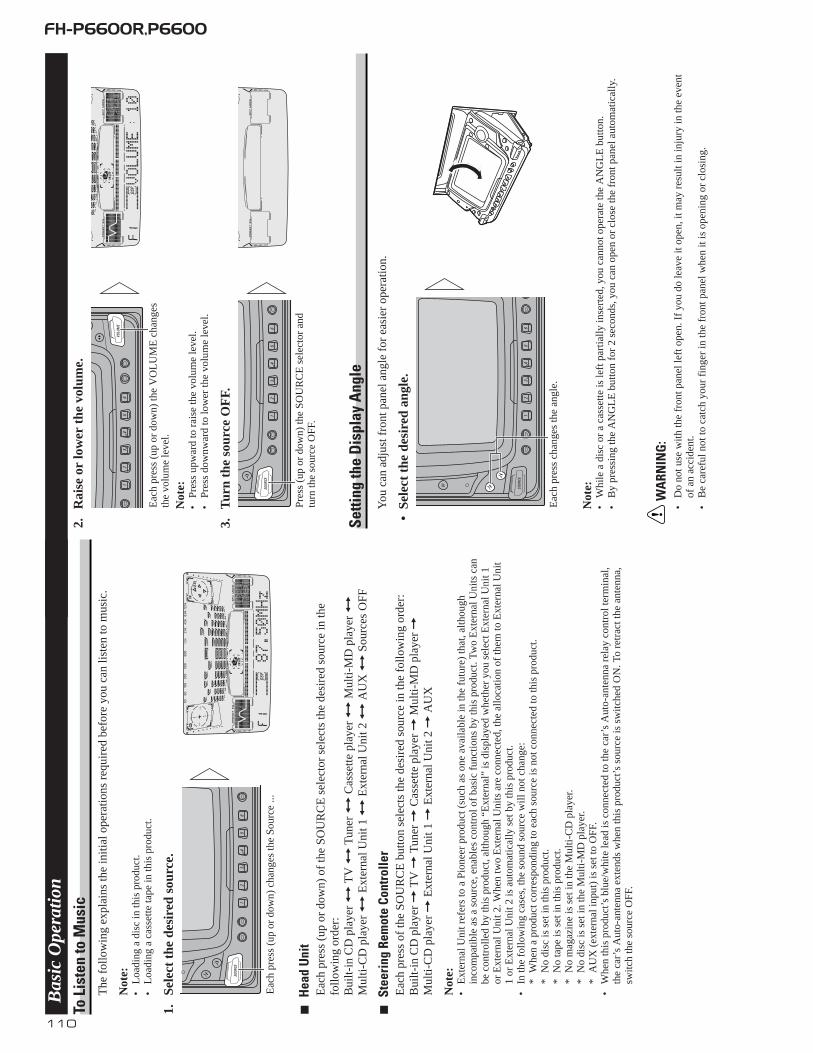
110
FH-P6600R,P6600
Bas
ic O
pera
tion
To L
iste
n to
Mus
icT
he f
ollo
win
g ex
plai
ns th
e in
itial
ope
ratio
ns r
equi
red
befo
re y
ou c
an li
sten
to m
usic
.
Not
e:•
Loa
ding
a d
isc
in th
is p
rodu
ct.
•L
oadi
ng a
cas
sette
tape
in th
is p
rodu
ct.
1.Se
lect
the
des
ired
sou
rce.
7H
ead
Uni
tE
ach
pres
s (u
p or
dow
n) o
f th
e SO
UR
CE
sel
ecto
r se
lect
s th
e de
sire
d so
urce
in th
e fo
llow
ing
orde
r:B
uilt-
in C
D p
laye
r Ô
TV
ÔT
uner
ÔC
asse
tte p
laye
r Ô
Mul
ti-M
D p
laye
r Ô
Mul
ti-C
D p
laye
r Ô
Ext
erna
l Uni
t 1 Ô
Ext
erna
l Uni
t 2 Ô
AU
X Ô
Sour
ces
OFF
7St
eeri
ng R
emot
e Co
ntro
ller
Eac
h pr
ess
of th
e SO
UR
CE
but
ton
sele
cts
the
desi
red
sour
ce in
the
follo
win
g or
der:
Bui
lt-in
CD
pla
yer
=T
V =
Tun
er =
Cas
sette
pla
yer
=M
ulti-
MD
pla
yer
=
Mul
ti-C
D p
laye
r =
Ext
erna
l Uni
t 1 =
Ext
erna
l Uni
t 2 =
AU
X
Not
e:•
Ext
erna
l Uni
t ref
ers
to a
Pio
neer
pro
duct
(su
ch a
s on
e av
aila
ble
in th
e fu
ture
) th
at, a
lthou
gh
inco
mpa
tible
as
a so
urce
, ena
bles
con
trol
of
basi
c fu
nctio
ns b
y th
is p
rodu
ct. T
wo
Ext
erna
l Uni
ts c
anbe
con
trol
led
by th
is p
rodu
ct, a
lthou
gh “
Ext
erna
l” is
dis
play
ed w
heth
er y
ou s
elec
t Ext
erna
l Uni
t 1or
Ext
erna
l Uni
t 2. W
hen
two
Ext
erna
l Uni
ts a
re c
onne
cted
, the
allo
catio
n of
them
to E
xter
nal U
nit
1 or
Ext
erna
l Uni
t 2 is
aut
omat
ical
ly s
et b
y th
is p
rodu
ct.
•In
the
follo
win
g ca
ses,
the
soun
d so
urce
will
not
cha
nge:
*W
hen
a pr
oduc
t cor
resp
ondi
ng to
eac
h so
urce
is n
ot c
onne
cted
to th
is p
rodu
ct.
*N
o di
sc is
set
in th
is p
rodu
ct.
*N
o ta
pe is
set
in th
is p
rodu
ct.
*N
o m
agaz
ine
is s
et in
the
Mul
ti-C
D p
laye
r.*
No
disc
is s
et in
the
Mul
ti-M
D p
laye
r.*
AU
X (
exte
rnal
inpu
t) is
set
to O
FF.
•W
hen
this
pro
duct
’s b
lue/
whi
te le
ad is
con
nect
ed to
the
car’
s A
uto-
ante
nna
rela
y co
ntro
l ter
min
al,
the
car’
s A
uto-
ante
nna
exte
nds
whe
n th
is p
rodu
ct’s
sou
rce
is s
witc
hed
ON
. To
retr
act t
he a
nten
na,
switc
h th
e so
urce
OFF
.
Eac
h pr
ess
(up
or d
own)
cha
nges
the
Sour
ce ..
.
2.R
aise
or
low
er t
he v
olum
e.
Not
e:•
Pres
s up
war
d to
rai
se th
e vo
lum
e le
vel.
•Pr
ess
dow
nwar
d to
low
er th
e vo
lum
e le
vel.
3.Tu
rn t
he s
ourc
e O
FF.
Setti
ng th
e D
ispl
ay A
ngle
You
can
adj
ust f
ront
pan
el a
ngle
for
eas
ier
oper
atio
n.
•Se
lect
the
des
ired
ang
le.
Not
e:•
Whi
le a
dis
c or
a c
asse
tte is
left
par
tially
inse
rted
, you
can
not o
pera
te th
e A
NG
LE
but
ton.
•B
y pr
essi
ng th
e A
NG
LE
but
ton
for
2 se
cond
s, y
ou c
an o
pen
or c
lose
the
fron
t pan
el a
utom
atic
ally
.
WA
RNIN
G:
•D
o no
t use
with
the
fron
t pan
el le
ft o
pen.
If
you
do le
ave
it op
en, i
t may
res
ult i
n in
jury
in th
e ev
ent
of a
n ac
cide
nt.
•B
e ca
refu
l not
to c
atch
you
r fi
nger
in th
e fr
ont p
anel
whe
n it
is o
peni
ng o
r cl
osin
g.
Eac
h pr
ess
chan
ges
the
angl
e.
Pres
s (u
p or
dow
n) th
e SO
UR
CE
sel
ecto
r an
dtu
rn th
e so
urce
OFF
.
Eac
h pr
ess
(up
or d
own)
the
VO
LU
ME
cha
nges
the
volu
me
leve
l.

111
FH-P6600R,P6600
Ope
n/Ej
ect
Pres
s th
e C
D E
JEC
T b
utto
n, a
nd th
e fr
ont p
anel
ope
ns, t
hen
the
disc
is e
ject
ed.
Whe
n a
CD
is n
ot in
sert
ed, b
y pr
essi
ng th
e C
DE
JEC
T b
utto
n, y
ouca
n op
en o
r cl
ose
the
fron
t pan
el a
ltern
atel
y.
Not
e:•
The
CD
func
tion
can
be tu
rned
ON
/OFF
with
the
disc
rem
aini
ng in
this
prod
uct.
•A
dis
c le
ft p
artia
lly in
sert
ed a
fter
eje
ctio
n m
ay in
cur
dam
age
or f
all o
ut.
Bas
ic O
pera
tion
Dis
c Lo
adin
g Sl
otIf
a C
D is
inse
rted
, the
fro
nt p
anel
is c
lose
d au
tom
atic
ally
.
Not
e:•
The
Bui
lt-in
CD
pla
yer
play
s on
e st
anda
rd 1
2 cm
or
8 cm
(si
ngle
) C
D a
t a ti
me.
Do
not u
se a
n ad
apte
r w
hen
play
ing
8 cm
CD
.
Not
e:•
If a
dis
c ca
nnot
be
inse
rted
ful
ly o
r pl
ayba
ck f
ails
, mak
e su
re th
e re
cord
ed s
ide
isdo
wn.
Pus
h th
e C
D E
JEC
T b
utto
n an
d ch
eck
the
disc
for
dam
age
befo
re
rein
sert
ing
it.•
If th
e B
uilt-
in C
D p
laye
r ca
nnot
ope
rate
pro
perl
y, a
n er
ror
mes
sage
(su
ch a
s“E
RR
OR
-14”
) ap
pear
s on
the
disp
lay.
Ref
er to
“B
uilt-
in C
D P
laye
r’s
Err
orM
essa
ge”.
WA
RNIN
G:
•D
o no
t use
with
the
fron
t pan
el le
ft o
pen.
If
you
do le
ave
it op
en, i
tm
ay r
esul
t in
inju
ry in
the
even
t of
an a
ccid
ent.
Bas
ic O
pera
tion
of B
uilt-
in C
D P
laye
r
Play
Tim
e In
dica
tor
Trac
k N
umbe
r Ind
icat
or
Switc
hing
the
Dis
play
Eac
h pr
ess
of th
e D
ISPL
AY
but
ton
chan
ges
the
disp
lay
in th
e fo
llow
ing
orde
r:Pl
ayba
ck m
ode
(Pla
y T
ime)
=D
isc
Titl
e (D
ISC
TIT
LE
)
Not
e:•
If y
ou s
witc
h a
disp
lay
whe
n th
e di
sc ti
tle h
as n
ot b
een
inpu
t, “N
O T
ITL
E”
is d
ispl
ayed
.•
Whe
n pl
ayin
g a
CD
TE
XT
dis
c, r
efer
to “
Titl
e D
ispl
ay S
witc
hing
” an
d “T
itle
Scro
ll”.
•A
CD
TE
XT
dis
c is
a C
D f
eatu
ring
rec
orde
d te
xt in
form
atio
n su
ch a
s D
isc
Titl
e, A
rtis
t Nam
e an
d T
rack
Titl
e.
Trac
k Se
arch
and
Fas
t For
war
d/Re
vers
e
•Y
ou c
an s
elec
t be
twee
n T
rack
Sea
rch
or F
ast
forw
ard/
Rev
erse
by
pres
sing
the
2/3
butt
on f
or a
dif
fere
nt le
ngth
of
tim
e.
Tra
ck S
earc
h0.
5 se
cond
s or
less
Fast
for
war
d/R
ever
seC
ontin
ue p
ress
ing

112
FH-P6600R,P6600
Bas
ic O
pera
tion
Cass
ette
Loa
ding
Slo
tIf
a c
asse
tte ta
pe is
inse
rted
, the
fro
nt p
anel
is c
lose
d au
tom
atic
ally
.
Not
e:•
Indi
cato
r “M
ETA
L”
light
s w
hen
a m
etal
or
chro
me
tape
is in
sert
ed.
Not
hing
is d
ispl
ayed
for
a n
orm
al ta
pe.
WA
RNIN
G:
•D
o no
t use
with
the
fron
t pan
el le
ft o
pen.
If
you
do le
ave
it op
en, i
tm
ay r
esul
t in
inju
ry in
the
even
t of
an a
ccid
ent.
Fast
For
war
d/Re
win
d an
d M
usic
Sea
rch
•E
ach
pres
s of
the
3bu
tton
sel
ects
Fas
t F
orw
ard
or F
orw
ard-
Mus
ic S
earc
h.FF
(Fa
st F
orw
ard)
=F-
MS
(For
war
d-M
usic
Sea
rch)
=N
orm
al P
layb
ack
•E
ach
pres
s of
the
2bu
tton
sel
ects
Rew
ind
or R
ewin
d-M
usic
Sea
rch.
RE
W (
Rew
ind)
=R
-MS
(Rew
ind-
Mus
ic S
earc
h) =
Nor
mal
Pla
ybac
k
Not
e:•
Fast
For
war
d/R
ewin
d an
d M
usic
Sea
rch
can
be c
ance
led
by p
ress
ing
the
BA
ND
butto
n.
Bas
ic O
pera
tion
of C
asse
tte P
laye
r
Not
e:•
Be
sure
to c
lose
the
fron
t pan
el a
fter
load
ing
or e
ject
ing
a ca
sset
te.
Dir
ectio
n In
dica
tor
Ope
n/Ej
ect
Pres
s th
e TA
PE E
JEC
T b
utto
n, a
nd th
e fr
ont p
anel
ope
ns, t
hen
the
tape
is e
ject
ed.
Whe
n a
cass
ette
tape
is n
ot in
sert
ed, b
y pr
essi
ng th
e TA
PEE
JEC
Tbu
tton,
you
can
ope
n or
clo
se th
e fr
ont p
anel
alte
rnat
ely.
Not
e:•
The
Tap
efu
nctio
n ca
n be
turn
ed O
N/O
FF w
ith th
e ca
sset
te ta
pe r
emai
ning
in th
is p
rodu
ct.
Dir
ectio
n Ch
ange
Play
Tim
e In
dica
tor
Not
e:•
The
con
tinuo
us p
layb
ack
time
coun
t sta
rts
at “
00'0
0''”
at t
he f
ollo
win
g tim
es.
*W
hen
a ta
pe is
inse
rted
.*
Whe
n th
e ta
pe d
irec
tion
is c
hang
ed.
*W
hen
you
rew
ind
the
tape
sid
e cu
rren
tly p
layi
ng b
ack
to th
e be
ginn
ing.
•T
he c
ontin
uous
pla
ybac
k tim
e co
unt i
s ha
lted
whe
n fa
st-f
orw
ardi
ng/r
ewin
ding
and
whi
le th
e M
usic
Sea
rch
func
tion
is o
pera
ting.

113
FH-P6600R,P6600
Bas
ic O
pera
tion
Trac
k Se
arch
and
Fas
t For
war
d/Re
vers
e
•Y
ou c
an s
elec
t be
twee
n T
rack
Sea
rch
orF
ast
forw
ard/
Rev
erse
by
pres
sing
the
2/3
butt
on f
or a
dif
fere
nt le
ngth
of
tim
e.
Tra
ck S
earc
h0.
5 se
cond
s or
less
Fast
For
war
d/R
ever
seC
ontin
ue p
ress
ing
Play
Tim
e In
dica
tor
Dis
c Se
arch
Dis
c N
umbe
r Ind
icat
orTr
ack
Num
ber I
ndic
ator
Bas
ic O
pera
tion
of M
ulti-
CD P
laye
rT
his
prod
uct c
an c
ontr
ol a
Mul
ti-C
D p
laye
r (s
old
sepa
rate
ly).
Dis
c N
umbe
r Sea
rch
(for 6
-Dis
c, 1
2-D
isc
type
s)
•Y
ou c
an s
elec
t di
scs
dire
ctly
wit
h th
e 1
to 6
but
tons
. Jus
t pr
ess
the
num
ber
corr
espo
ndin
g to
the
dis
c yo
u w
ant
to li
sten
to.
Not
e:•
Whe
n a
12-D
isc
Mul
ti-C
D P
laye
r is
con
nect
ed a
nd y
ou w
ant t
o se
lect
dis
c 7
to 1
2, p
ress
the
1 to
6bu
ttons
for
2 s
econ
ds.
Not
e:•
The
Mul
ti-C
D p
laye
r m
ay p
erfo
rm a
pre
para
tory
ope
ratio
n, s
uch
as v
erif
ying
the
pres
ence
of
a di
scor
rea
ding
dis
c in
form
atio
n, w
hen
the
pow
er is
turn
ed O
N o
r a
new
dis
c is
sel
ecte
d fo
r pl
ayba
ck.
“RE
AD
Y”
is d
ispl
ayed
.•
If th
e M
ulti-
CD
pla
yer
cann
ot o
pera
te p
rope
rly,
an
erro
r m
essa
ge s
uch
as “
ER
RO
R-1
4” is
di
spla
yed.
Ref
er to
the
Mul
ti-C
D p
laye
r ow
ner’
s m
anua
l.•
If th
ere
are
no d
iscs
in th
e M
ulti-
CD
pla
yer
mag
azin
e, “
NO
DIS
C”
is d
ispl
ayed
.
Bas
ic O
pera
tion
of T
uner
Thi
s pr
oduc
t’s A
F fu
nctio
n ca
n be
sw
itche
d O
N a
nd O
FF. A
F sh
ould
be
switc
hed
OFF
for
norm
al tu
ning
ope
ratio
ns.
Man
ual a
nd S
eek
Tuni
ng
•Y
ou c
an s
elec
t th
e tu
ning
met
hod
by c
hang
ing
the
leng
th o
f ti
me
you
pres
s th
e 2
/3bu
tton
.
Man
ual T
unin
g (s
tep
by s
tep)
0.5
seco
nds
or le
ss
Seek
Tun
ing
0.5
seco
nds
or m
ore
Not
e:•
If y
ou c
ontin
ue p
ress
ing
the
butto
n fo
r lo
nger
than
0.5
sec
onds
, you
can
ski
p br
oadc
astin
gst
atio
ns. S
eek
Tun
ing
star
ts a
s so
on a
s yo
u re
leas
e th
e bu
tton.
•St
ereo
indi
cato
r “
” lig
hts
whe
n a
ster
eo s
tatio
n is
sel
ecte
d.
Pres
et T
unin
g
•Y
ou c
an m
emor
ize
broa
dcas
t st
atio
ns in
but
tons
1 th
roug
h 6
for
easy
, one
-tou
ch s
tati
on r
ecal
l.
Pres
et s
tatio
n re
call
2 se
cond
s or
less
Bro
adca
st s
tatio
n pr
eset
mem
ory
2 se
cond
s or
mor
e
Not
e:•
Up
to 1
8 FM
sta
tions
(6
in F
1 (F
M1)
, F2
(FM
2) a
nd F
3(F
M3)
) an
d 6
MW
/LW
sta
tions
can
be
stor
ed in
mem
ory.
•Y
ou c
an a
lso
use
the
5or
∞bu
ttons
to r
ecal
l bro
adca
stst
atio
ns m
emor
ized
in b
utto
ns 1
thro
ugh
6.
Freq
uenc
y In
dica
tor
Ban
d In
dica
tor
Ban
d F1 (
FM1)
=F2
(FM
2)=
F3 (
FM3)
=M
W/L
W
Pres
et N
umbe
r Ind
icat
or

114
FH-P6600R,P6600-
(FH
-P6600R
/EW
)
+ ≠
+ ≠
+ ≠
+ ≠
1*
2* 4*
3* 5*
IP-B
US
cabl
e
Blu
e/w
hite
Syst
emre
mot
eco
ntro
l
Pow
eram
p(s
old
sepa
rate
ly)
Subw
oofe
rSu
bwoo
fer
Fron
tspe
aker
Fron
tspe
aker
Perf
orm
thes
eco
nnec
tions
whe
nus
ing
adi
ffer
enta
mp
(sol
dse
para
tely
).
Pow
eram
p(s
old
sepa
rate
ly)
Yel
low
/bla
ckIf
you
use
ace
llula
rte
leph
one,
conn
ecti
tvia
the
Aud
ioM
ute
lead
onth
ece
llula
rte
leph
one.
Ifno
t,ke
epth
eA
udio
Mut
ele
adfr
eeof
any
conn
ectio
ns.
Con
nect
lead
sof
the
sam
eco
lor
toea
chot
her.
Cap
(1*)
Whe
nno
tusi
ngth
iste
rmin
al,
dono
trem
ove
the
cap.
ISO
conn
ecto
r
Fuse
hold
erY
ello
w(2
*)To
term
inal
alw
ays
supp
lied
with
pow
erre
gard
less
ofig
nitio
nsw
itch
posi
tion.
Red
(4*)
Toel
ectr
icte
rmin
alco
ntro
lled
byig
nitio
nsw
itch
(12
VD
C)
ON
/OFF
.
Yel
low
(3*)
Bac
k-up
(or
acce
ssor
y)
Red
(5*)
Acc
esso
ry(o
rba
ck-u
p)
Bla
ck(g
roun
d)To
vehi
cle
(met
al)
body
.
Ora
nge
Tolig
htin
gsw
itch
term
inal
.
Not
e:In
som
eve
hicl
es,t
heIS
Oco
nnec
tor
may
bedi
vide
din
totw
o.In
this
case
,be
sure
toco
nnec
tto
both
conn
ecto
rs.
Con
nect
ing
cord
sw
ithR
CA
pin
plug
s(s
old
sepa
rate
ly)
Fuse
resi
stor
Fuse
resi
stor
Blu
e/w
hite
(7*)
Blu
e/w
hite
(6*)
Spea
ker
lead
sW
hite
Whi
te/b
lack
Gra
yG
ray/
blac
k
:Fro
ntle
ft+
:Fro
ntle
ft≠
:Fro
ntri
ght +
:Fro
ntri
ght ≠
Gre
enG
reen
/bla
ckV V
iole
tio
let/b
lack
:Rea
rle
ft+
:Rea
rle
ft≠
:Rea
rri
ght +
:Rea
rri
ght ≠
Tosy
stem
cont
rolt
erm
inal
ofth
epo
wer
amp
(max
.300
mA
12V
DC
).
ToA
uto-
ante
nna
rera
yco
ntro
lte
rmin
al(m
ax.3
00m
A12
VD
C).
Not
e:D
epen
ding
onth
eki
ndof
vehi
cle,
the
func
tion
of3*
and
5*m
aybe
diff
eren
t.In
this
case
,be
sure
toco
nnec
t2*
to5*
and
4*to
3*.
The
pin
posi
tion
ofth
eIS
Oco
nnec
tor
will
diff
erde
pend
son
the
type
ofve
hicl
e.C
onne
ct6*
and
7*w
hen
Pin
5is
anan
tenn
aco
ntro
ltyp
e. I
nan
othe
rty
peof
vehi
cle,
neve
rco
nnec
t6*
and
7*.
Mul
ti-C
Dpl
ayer
(sol
dse
para
tely
)
Fron
tout
put
Subw
oofe
rou
tput
orR
ear
outp
ut
Thi
sPr
oduc
t
Ant
enna
jack
IP-B
US
inpu
t(B
lue)

115
FH-P6600R,P6600
-(F
H-P
6600/E
S)
+ ≠
+ ≠
+ ≠
+ ≠
+ ≠
+ ≠
+ ≠
+ ≠
Subw
oofe
rou
tput
orR
ear
outp
ut
Thi
sPr
oduc
t
Mul
ti-C
Dpl
ayer
(sol
dse
para
tely
) IP-B
US
cabl
e
Con
nect
ing
cord
sw
ithR
CA
pin
plug
s(s
old
sepa
rate
ly)
Syst
emre
mot
eco
ntro
l
Pow
eram
p(s
old
sepa
rate
ly)
Fron
tout
put
Subw
oofe
ror
Rea
rsp
eake
rSu
bwoo
fer
orR
ear
spea
ker
Rig
ht
Fron
tspe
aker
Rea
rsp
eake
r
Whi
teG
ray
Whi
te/b
lack
Gre
en
Gre
en/b
lack
Gra
y/bl
ack
Vio
let
Vio
let/b
lack
Fron
tspe
aker
Rea
rsp
eake
r
Left
Fron
tspe
aker
Fron
tspe
aker
Perf
orm
thes
eco
nnec
tions
whe
nus
ing
adi
ffer
enta
mp
(sol
dse
para
tely
).
With
a2
spea
ker
syst
em,d
ono
tcon
nect
anyt
hing
toth
esp
eake
rle
ads
that
are
not
conn
ecte
dto
spea
kers
.
Yel
low
Tote
rmin
alal
way
ssu
pplie
dw
ithpo
wer
rega
rdle
ssof
igni
tion
switc
hpo
sitio
n.
Ora
nge
Tolig
htin
gsw
itch
term
inal
.
Red
Toel
ectr
icte
rmin
alco
ntro
lled
byig
nitio
nsw
itch
(12
VD
C)
ON
/OFF
.
Pow
eram
p(s
old
sepa
rate
ly)
Yel
low
/bla
ckIf
you
use
ace
llula
rte
leph
one,
conn
ecti
tvia
the
Aud
ioM
ute
lead
onth
ece
llula
rte
leph
one.
Ifno
t,ke
epth
eA
udio
Mut
ele
adfr
eeof
any
conn
ectio
ns.
Bla
ck(g
roun
d)To
vehi
cle
(met
al)
body
.
Fuse
hold
er
Ant
enna
jack
Fuse
resi
stor
Fuse
resi
stor
Blu
eW
hen
the
sour
ceis
sele
cted
the
tune
r,a
cont
rols
igna
lis
outp
ut.
ToA
uto-
ante
nna
rela
yco
ntro
lter
min
al.
Ifth
eca
rfe
atur
esa
glas
san
tenn
a,co
nnec
tto
the
ante
nna
boos
ter
pow
ersu
pply
term
inal
(max
.300
mA
12V
DC
).
Blu
e/w
hite
Whe
nth
eso
urce
issw
itche
dO
N,
aco
ntro
lsig
nali
sou
tput
.To
syst
emco
ntro
lter
min
alof
the
pow
eram
p(m
ax.3
00m
A12
VD
C).
IP-B
US
inpu
t(B
lue)

FH-P6600R,P6600
GeneralPower source .......... 14.4 V DC (10.8 – 15.1 V allowable)Grounding system ........................................ Negative typeMax. current consumption ...................................... 10.0 ADimensions
(mounting size) .... 178 (W) × 100 (H) × 160 (D) mm(front face) .............. 170 (W) × 95 (H) × 18 (D) mm
Weight ...................................................................... 3.0 kg
Audio/DSP(FH-P6600R/EW)Maximum power output ...................................... 45 W × 4Continuous power output .................................... 27 W × 4Load impedance .......................... 4 Ω (4 – 8 Ω allowable)Preout maximum output level/
output impedance ........................................ 2 V/1 kΩLoudness contour ........ +10 dB (100 Hz), +7 dB (10 kHz)
(volume: –30 dB)Equalizer (11-Band Graphic Equalizer)
Frequency ........................ 50/80/160/250/500/800 Hz1.2/2.5/4/8/12.5 kHz
Equalization range .......................................... ±12 dBHPF
Frequency ............................................ 50/80/125 HzSlope ........................................................ –12 dB/oct.
Subwoofer outputFrequency ............................................ 50/80/125 HzSlope ........................................................ –18 dB/oct.Gain .................................................................. ±6 dBPhase ................................................ Normal/Reverse
Audio/DSP(FH-P6600/ES)Continuous power output is 22 W per channel min. into 4ohms, both channels driven 50 to 15,000 Hz with no morethan 5% THD.Maximum power output ...................................... 45 W × 4Load impedance .......................... 4 Ω (4 – 8 Ω allowable)Preout maximum output level/
output impedance ........................................ 2 V/1 kΩLoudness contour ........ +10 dB (100 Hz), +7 dB (10 kHz)
(volume: –30 dB)Equalizer (11-Band Graphic Equalizer)
Frequency ........................ 50/80/160/250/500/800 Hz1.2/2.5/4/8/12.5 kHz
Equalization range .......................................... ±12 dBHPF
Frequency ............................................ 50/80/125 HzSlope ........................................................ –12 dB/oct.
Subwoofer outputFrequency ............................................ 50/80/125 HzSlope ........................................................ –18 dB/oct.Gain ................................................................ ±12 dB
CD playerSystem .................................... Compact disc audio systemUsable discs .................................................. Compact discSignal format .................... Sampling frequency: 44.1 kHz
Number of quantization bits: 16; linearFrequency characteristics .............. 5 – 20,000 Hz (±1 dB)Signal-to-noise ratio ...... 94 dB (1 kHz) (IEC-A network)Dynamic range ............................................ 92 dB (1 kHz)Number of channels ............................................ 2 (stereo)
Cassette playerTape ........................ Compact cassette tape (C-30 – C-90)Tape speed ........ 4.76 cm/sec.(+0.14cm/sec.,–0.05cm/sec.)Fast forward/rewinding time .... Approx. 100 sec. for C-60Wow & flutter .......................................... 0.09% (WRMS)Frequency response .......... Metal: 30 – 19,000 Hz (±3 dB)Stereo separation ...................................................... 50 dBSignal-to-noise ratio
...... Metal: Dolby B NR IN: 67 dB (IEC-A network)Dolby NR OUT: 61 dB (IEC-A network)
FM tunerFrequency range ...................................... 87.5 – 108 MHzUsable sensitivity .................................................... 10 dBf
(1.0 µV/75 Ω, mono, S/N: 30 dB)50 dB quieting sensitivity ........................................ 15 dBf
(1.7 µV/75 Ω, mono)Signal-to-noise ratio ...................... 70 dB (IEC-A network)Distortion .......................... 0.3% (at 65 dBf, 1 kHz, stereo)Frequency response ...................... 30 – 15,000 Hz (±3 dB)Stereo separation .......................... 40 dB (at 65 dBf, 1 kHz)
MW tuner(FH-P6600R/EW)Frequency range .......................... 531 – 1602 kHz (9 kHz)Usable sensitivity .............................. 18 µV (S/N: 20 dB)Selectivity .................................................. 50 dB (±9 kHz)
LW tuner(FH-P6600R/EW)Frequency range ........................................ 153 – 281 kHzUsable sensitivity .............................. 30 µV (S/N: 20 dB)Selectivity .................................................. 50 dB (±9 kHz)
AM tuner(FH-P6600/ES)Frequency range ........................ 531 – 1,602 kHz (9 kHz)
530 – 1,640 kHz (10 kHz)Usable sensitivity .............................. 18 µV (S/N: 20 dB)Selectivity .................................................. 50 dB (±9 kHz)
50 dB (±10 kHz)
Note:• Specifications and the design are subject to
possible modification without notice due toimprovements.
8.2 SPECIFICATIONS