Ferroelectric materials for piezoelectric, pyroelectric, and
51
1 Ferroelectric materials for piezoelectric, pyroelectric, and memory applications Marin Alexe Max Planck Institute of Microstructure Physics Halle – Germany Outline Introduction Basics of Ferroelectricity – Applications – Definitions Ferroelectric materials for – Piezoelectric applications – Non-volatile memories – Pyroelectric applications * Electrical characterization Nanoscale ferroelectrics * With the kind contribution of Paul Muralt, EPFL, Lausanne CH
Transcript of Ferroelectric materials for piezoelectric, pyroelectric, and
1
Ferroelectric materials for piezoelectric, pyroelectric, and memory applications
Marin AlexeMax Planck Institute of Microstructure PhysicsHalle – Germany
Outline
Introduction Basics of Ferroelectricity– Applications– Definitions
Ferroelectric materials for– Piezoelectric applications– Non-volatile memories– Pyroelectric applications *
Electrical characterization Nanoscale ferroelectrics
* With the kind contribution of Paul Muralt, EPFL, Lausanne CH

2
Outline
Textbook– Ferroelectric crystals, F. Jona and G. Shirane, Pergamon, Oxford 1962– Physical properties of crystals, J. F. Nye, Clarendon, Oxford, 1964– Principles and Applications of Ferroelectric Crystals …, M.E. Lines and A.M. Glass,
Clarendon, Oxford 1977– Ferroelectric memories, J. F. Scott, Berlin, Springer, 2000– Ferroelectric devices, K. Uchino, Dekker, 2000– Nanoelectronics and Information Technology, R. Waser (ed). Wiley-VCH, 2003
Edited books– Thin film ferroelectric materials and devices, R. Ramesh (ed.), Kluwer, 1997– Ferroelectric thin films : synthesis and basic properties, Paz de Araujo, Scott, and Taylor,
Gordon and Breach, 1996– Nanoscale phenomena in ferroelectric thin films, S. Hong (ed), Kluwer, 2004– Nanoscale characterisation of ferroelectric materials : scanning probe microscopy
approach, Alexe and Gruverman (eds), Springer, 2004Databases
– Landolt-Börnstein, vol. 16, Ferroelectric and related substances, ed. E. Nakamura, Springer, 1981
Review papers– The physics of ferroelectric ceramic thin films for memory applications, J.F. Scott,
Ferroelectrics Review 1, 1 (1998)– Ferroelectric, dielectric and piezoelectric properties of ferroelectric thin films and
ceramics, D. Damianovici, Rep. Prog. Phys. (61)1267 (1998)– Physics of thin-film ferroelectric oxides, M. Dawber et al., Rev Mod. Phys., in press– M. Fiebig, Revival of the magnetoelectric effect, J. Phys. D, 38 (2005) R123 – etc.
Basics of Ferroelectrics

3
Applications
The physics of ferroelectric memories, Auciello O, Scott JF, Ramesh R., Physics Today 51, p22, July 1998
Applications
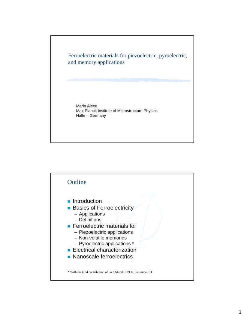
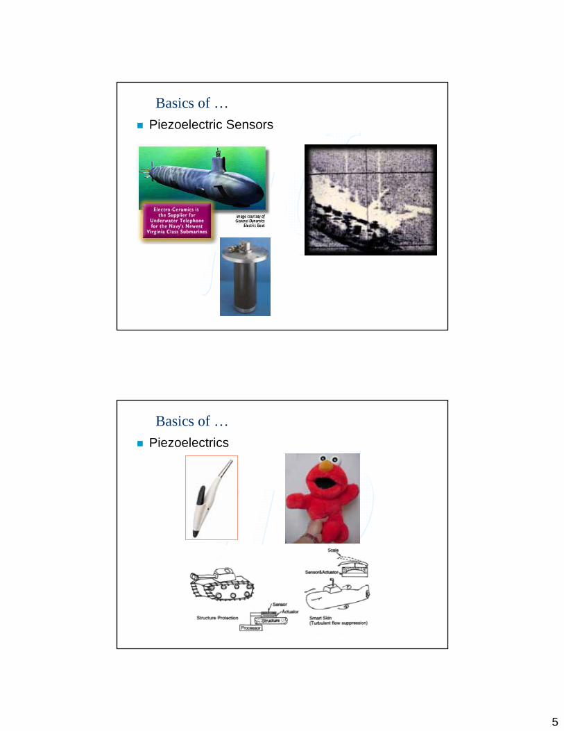
Piezoelectric Sensors/Actuators, MEMS
Pyroelectric Detectors/Sensors
Electro-optical switches and modulators
Optical Waveguides
Dynamic RAMs (capacitors)
Tunable Microwave Devices
Non-Volatile RAMs (memory)

4
Basics of ferroelectricity
Piezolectrics:– Charge generation by mechanical fields
Pyroelectrics:– Charge generation by thermal fields
Ferroelectrics:– Charge generation by electrical fields
Applications-What are they good for?
And converse !
Basics of …
What are they good for?Piezoelectrics– Mechanical strain (stress) ⇔ Electric field (charge)
Stress X
+Q
-Q
P
D= deffX
Di= dijkXjk
D – charge densitydeff – effective piezoelectric coeff.X – stress
5
Basics of … Piezoelectric Sensors
Basics of … Piezoelectrics
6
Basics of … Piezoelectric Actuators
Basics of …
What are they good for?Pyroelectrics– Thermal variation ⇔ Charge generation
∆T
+Q
-Q
P
∆Q=p∆T
7
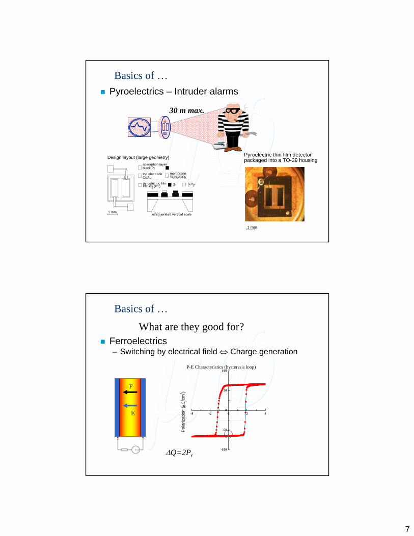
Basics of … Pyroelectrics – Intruder alarms
absorption layer black Pt
top electrode Cr/Au
pyroelectric film PbTiO3 (PT)
membrane Si3N4/SiO2
SiO2
Design layout (large geometry)
Si
exaggerated vertical scale1 mm
1 mm
Pyroelectric thin film detector packaged into a TO-39 housing
30 m max.
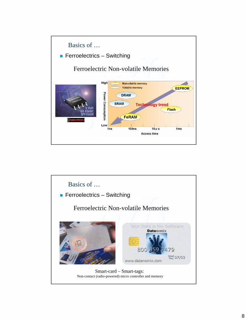
Ferroelectrics– Switching by electrical field ⇔ Charge generation
Basics of …
P
E
P-E Characteristics (hysteresis loop)
What are they good for?
∆Q=2Pr
-4 -2 0 2 4
-100
-50
0
50
100
Pola
rizat
ion
(µC
/cm
2 )
8
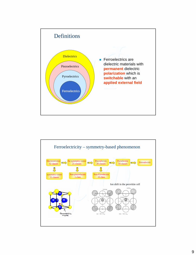
Ferroelectrics – Switching
Basics of …
Ferroelectric Non-volatile Memories
Ferroelectrics – Switching
Basics of …
Ferroelectric Non-volatile Memories
Smart-card – Smart-tags: Non-contact (radio-powered) micro controller and memory
9
Definitions
Ferroelectrics are dielectric materials with permanent dielectric polarization which is switchable with an applied external field
Dielectrics
Piezoelectrics
Pyroelectrics
FerroelectricsFerroelectrics
Ferroelectricity – symmetry-based phenomenon
Electrostrictive32 classes
No symmetry centre21 classes
Piezoelectric20 classes
Non-piezoelectric1 class
Pyroelectric10 classes
Non-Pyroelectric10 class
symmetry centre11 classes
Ferroelectric
Ion shift in the perovkite cell
10
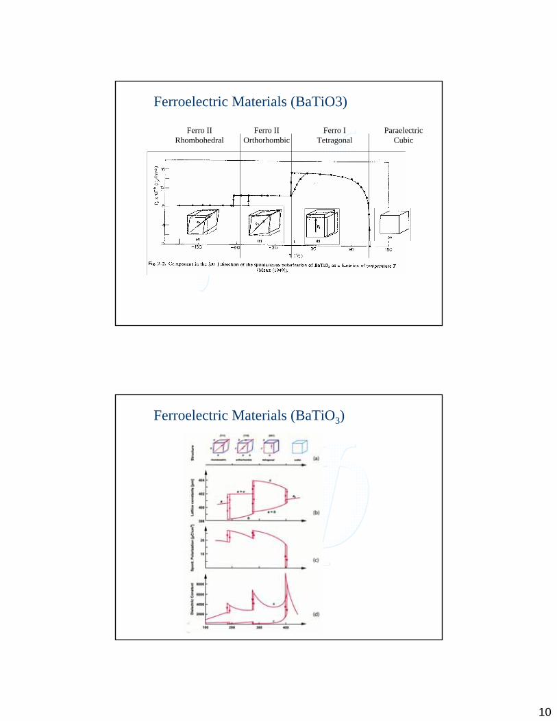
Ferroelectric Materials (BaTiO3)
ParaelectricCubic
Ferro ITetragonal
Ferro IIOrthorhombic
Ferro IIRhombohedral
Ferroelectric Materials (BaTiO3)
11
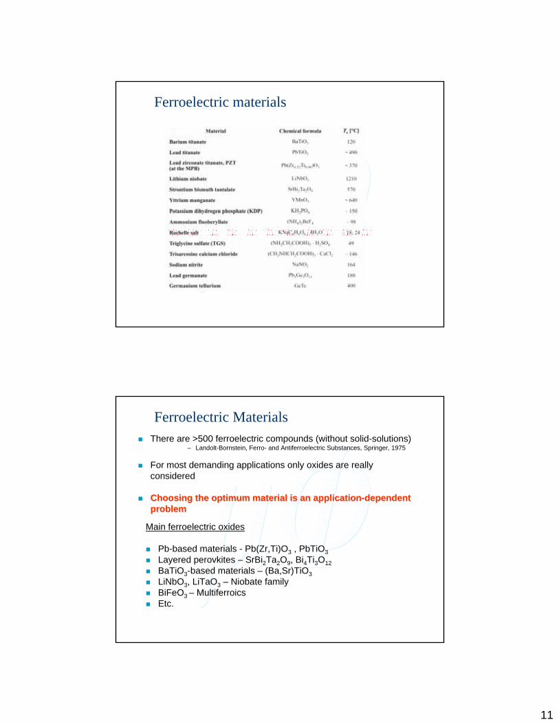
Ferroelectric materials
Ferroelectric Materials
Main ferroelectric oxides
Pb-based materials - Pb(Zr,Ti)O3 , PbTiO3Layered perovkites – SrBi2Ta2O9, Bi4Ti3O12BaTiO3-based materials – (Ba,Sr)TiO3LiNbO3, LiTaO3 – Niobate familyBiFeO3 – MultiferroicsEtc.
There are >500 ferroelectric compounds (without solid-solutions)– Landolt-Bornstein, Ferro- and Antiferroelectric Substances, Springer, 1975
For most demanding applications only oxides are really considered
Choosing the optimum material is an applicationChoosing the optimum material is an application--dependent dependent problemproblem
12
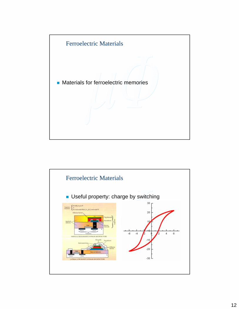
Ferroelectric Materials
Materials for ferroelectric memories
Ferroelectric Materials
Useful property: charge by switching
13
Ferroelectric Materials
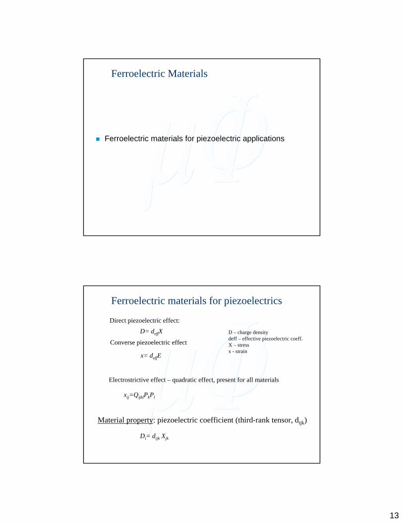
Ferroelectric materials for piezoelectric applications
Ferroelectric materials for piezoelectrics
Direct piezoelectric effect:D= deffX
Converse piezoelectric effect
x= deffE
D – charge densitydeff – effective piezoelectric coeff.X – stressx - strain
Material property: piezoelectric coefficient (third-rank tensor, dijk)
Electrostrictive effect – quadratic effect, present for all materials
xij=QijklPkPl
Di= dijk Xjk
14
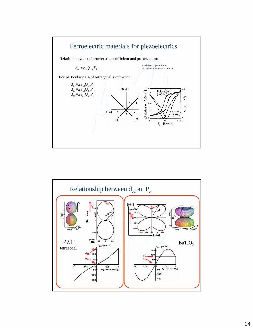
Ferroelectric materials for piezoelectrics
Relation between piezoelectric coefficient and polarization:
dim=εikQmikPk
For particular case of tetragonal symmetry:
d33=2ε33Q33P3d31=2ε33Q13P3d15=2ε11Q44P3
ε - dielectric permittivitym –index in the matrix notation
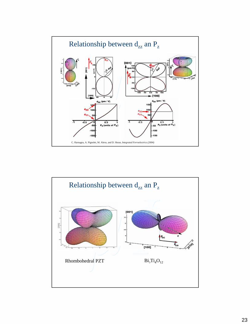
Relationship between dzz an Pz
PZTtetragonal
BaTiO3

15
Relationship between dzz an Pz
PZTrhombohedral
Ferroelectric materials for piezoelectric appl.
Figures of merit:
x=dEE=gX
d – actuator figure of meritg – sensor figure of merit
For polycrystalline materials depends on the sample symmetry:
Pd33
d31
Electromechanical coupling factor k
k2=Stored mechanical (electrical) energy/Stored electrical (mechanical) energy
g=d/ε
k2=d2/(εs) s – elastic stiffness
16
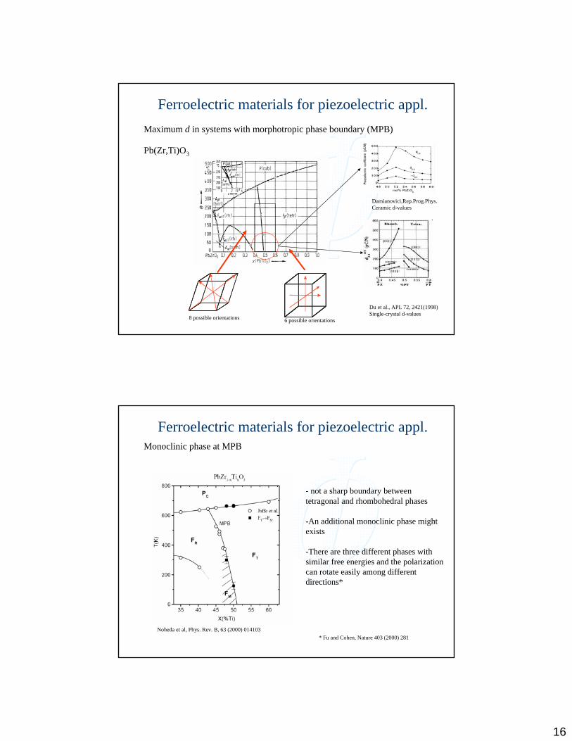
Ferroelectric materials for piezoelectric appl. Maximum d in systems with morphotropic phase boundary (MPB)
Pb(Zr,Ti)O3
Du et al., APL 72, 2421(1998)Single-crystal d-values
Damianovici,Rep.Prog.Phys.Ceramic d-values
6 possible orientations8 possible orientations
Ferroelectric materials for piezoelectric appl. Monoclinic phase at MPB
Noheda et al, Phys. Rev. B, 63 (2000) 014103
- not a sharp boundary between tetragonal and rhombohedral phases
-An additional monoclinic phase might exists
-There are three different phases with similar free energies and the polarizationcan rotate easily among different directions*
* Fu and Cohen, Nature 403 (2000) 281
17
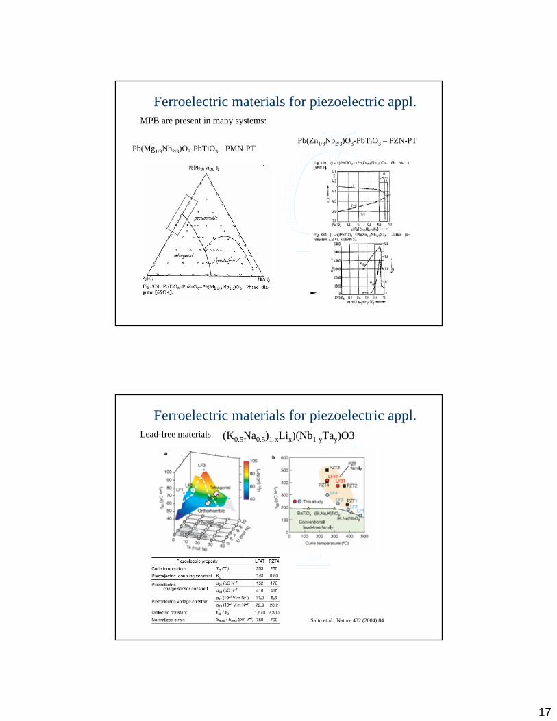
Ferroelectric materials for piezoelectric appl. MPB are present in many systems:
Pb(Zn1/3Nb2/3)O3-PbTiO3 – PZN-PT Pb(Mg1/3Nb2/3)O3-PbTiO3 – PMN-PT
Ferroelectric materials for piezoelectric appl. Lead-free materials (K0.5Na0.5)1-xLix)(Nb1-yTay)O3
Saito et al., Nature 432 (2004) 84
18
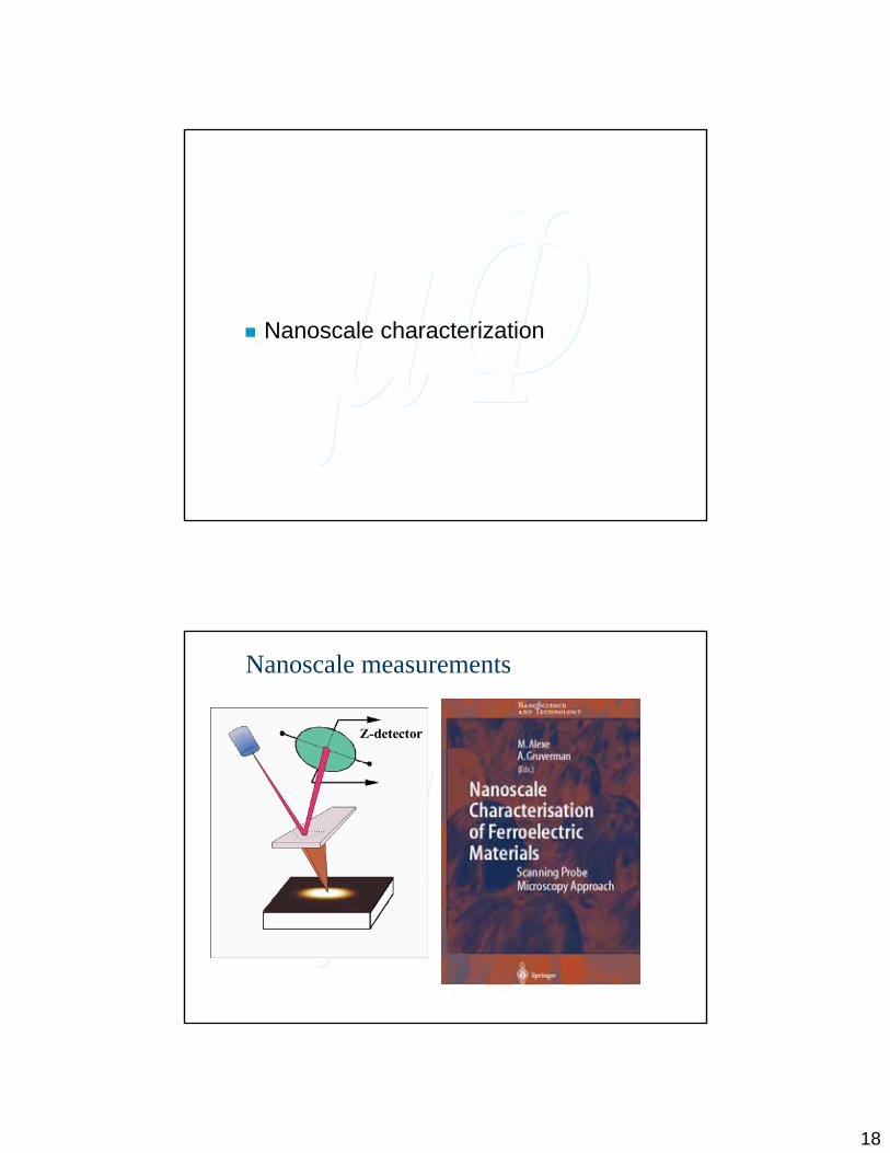
Nanoscale characterization
Nanoscale measurements
19
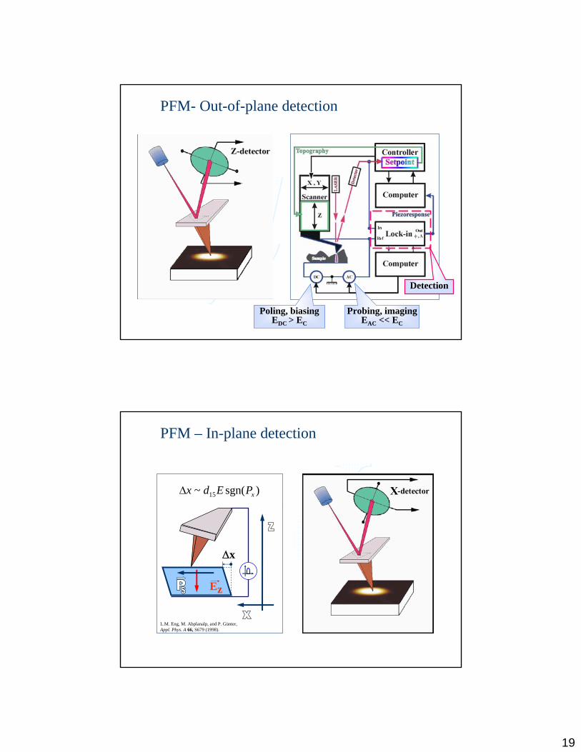
PFM- Out-of-plane detection
Poling, biasingEDC > EC
Probing, imagingEAC << EC
Detection
PFM – In-plane detection
L.M. Eng, M. Abplanalp, and P. Günter, Appl. Phys. A 66, S679 (1998).
∆x
Ez
)sgn(~ 15 xPEdx∆
20
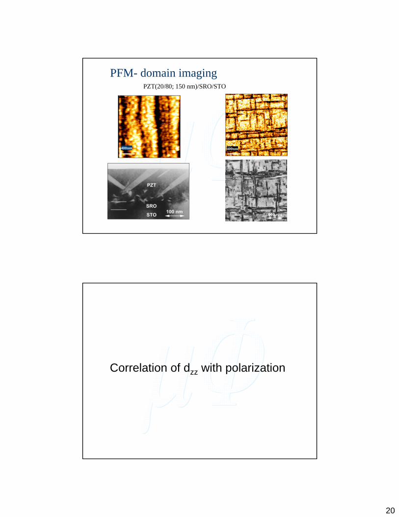
PZT(20/80; 150 nm)/SRO/STO
400nm400nm
PFM- domain imaging
Correlation of dzz with polarization
21
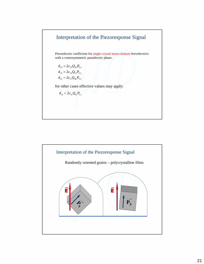
Interpretation of the Piezoresponse Signal
Piezoelectric coefficient for single-crystal mono-domain ferroelectrics with a centrosymmetric paraelectric phase:
3441115
3133331
3333333
222
S
S
S
PQdPQdPQd
εεε
=
=
=
for other cases effective values may apply:
zSzzzzzz PQd ε2=
PSPS
Interpretation of the Piezoresponse Signal
Randomly oriented grains – polycrystalline films

22
Calculations were made for PZT (30/70) using data from: M.J. Haun, E. Furman, S.J. Jang, and L.E. Cross, Ferroelectr. 99, 13 (1989).
θθθθ 333
21531 coscossin)()( ddddzz ++=
[001
] (pm
/V)
[010](pm/V)
(pm/V)
(pm
/V)
(pm/V)
The piezoelectric “surface” for PZT
PSPS
Effect of the orientation on hysteresis
dzz NOT directly proportional to Pz !
23
Relationship between dzz an Pz
C. Harnagea, A. Pignolet, M. Alexe, and D. Hesse, Integrated Ferroelectrics (2004)
Relationship between dzz an Pz
Rhombohedral PZT Bi3Ti4O12
24
Pyroelectrics
* With the kind contribution of Paul Muralt, EPFL, Lausanne CH
Intruder alarm
absorption layer black Pt
top electrode Cr/Au
pyroelectric film PbTiO 3 (PT)
membrane Si3N4/SiO 2
SiO2
Design layout (large geometry)
Si
exaggerated vertical scale1 mm
1 mm
Pyroelectric thin film detector packaged into a TO-39 housing
30 m max. Bell 1994, Kohli 1997
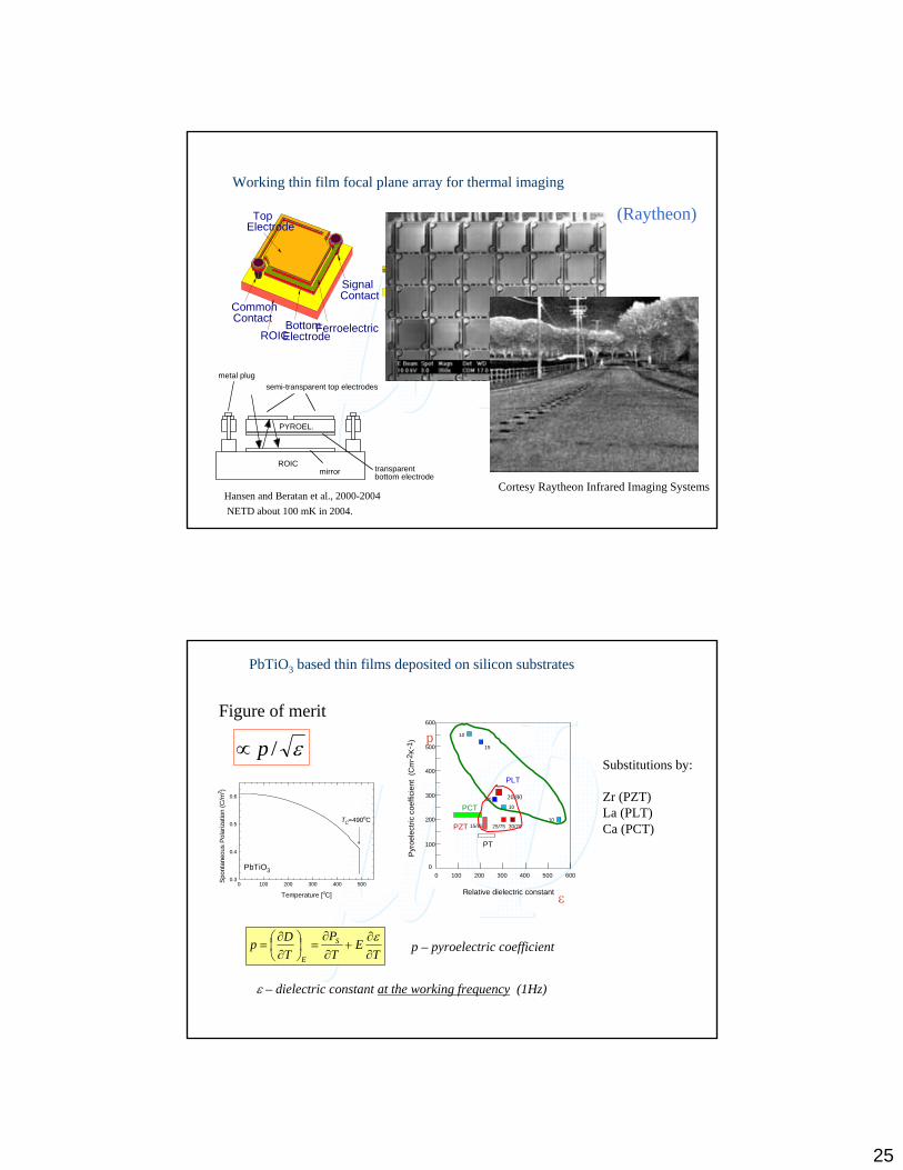
25
Working thin film focal plane array for thermal imaging
ROIC
PYROEL.
mirror
semi-transparent top electrodes
transparent bottom electrode
metal plug
Cortesy Raytheon Infrared Imaging Systems
NETD about 100 mK in 2004.Hansen and Beratan et al., 2000-2004
SignalContact
BottomElectrode
Ferroelectric
TopElectrode
CommonContact
ROIC
(Cross S
(Raytheon)
PbTiO3 based thin films deposited on silicon substrates
Substitutions by:
Zr (PZT)La (PLT)Ca (PCT)
p – pyroelectric coefficient
Figure of merit
ε/p∝
Relative dielectric constant
Pyro
elec
tric
coef
ficie
nt (
Cm
-2K
-1)
300
100
200
400
500
600
0100 200 300 400 500 6000
PT
15/85 25/75 30/70
10
PZT
15
PLT
20
10
10
PCT20/80
p
ε0 100 200 300 400 500
0.3
0.4
0.5
0.6
PbTiO3
TC=490oC
Spon
tane
ous
Pola
rizat
ion
(C/m
2 )
Temperature [oC]
TE
TP
TDp S
E ∂∂
+∂∂
=⎟⎠⎞
⎜⎝⎛
∂∂
=ε
ε – dielectric constant at the working frequency (1Hz)
26
Electro-optic materials
* With the kind contribution of Paul Muralt, EPFL, Lausanne CH
Electro-optic materials
Electrooptic (and acoustooptic) effects are of considerable practical importance as they can be used to:
– modulate (amplitude and phase) light beams
– shift the light frequency
– alter the direction in which the beam travels
27
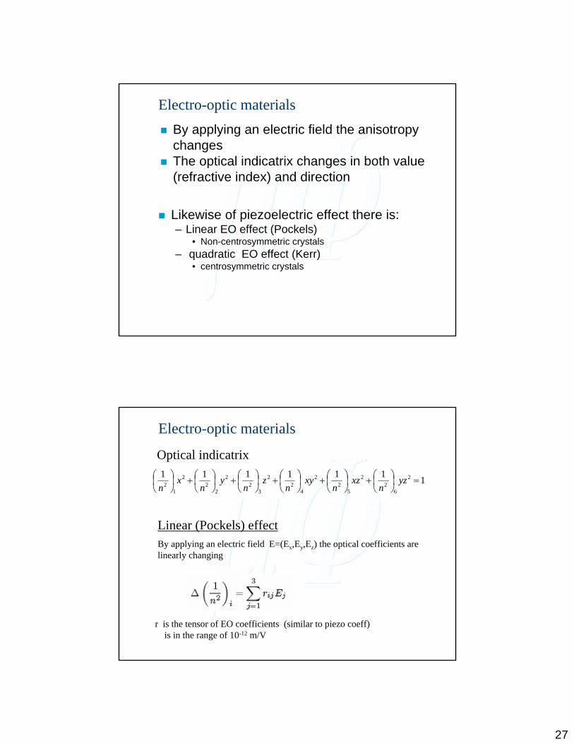
Electro-optic materials
Likewise of piezoelectric effect there is:– Linear EO effect (Pockels)
• Non-centrosymmetric crystals– quadratic EO effect (Kerr)
• centrosymmetric crystals
By applying an electric field the anisotropy changesThe optical indicatrix changes in both value (refractive index) and direction
Electro-optic materials
1111111 2
62
2
52
2
42
2
32
2
22
2
12 =⎟
⎠⎞
⎜⎝⎛+⎟
⎠⎞
⎜⎝⎛+⎟
⎠⎞
⎜⎝⎛+⎟
⎠⎞
⎜⎝⎛+⎟
⎠⎞
⎜⎝⎛+⎟
⎠⎞
⎜⎝⎛ yz
nxz
nxy
nz
ny
nx
n
Optical indicatrix
By applying an electric field E=(Ex,Ey,Ez) the optical coefficients are linearly changing
Linear (Pockels) effect
r is the tensor of EO coefficients (similar to piezo coeff)is in the range of 10-12 m/V
28
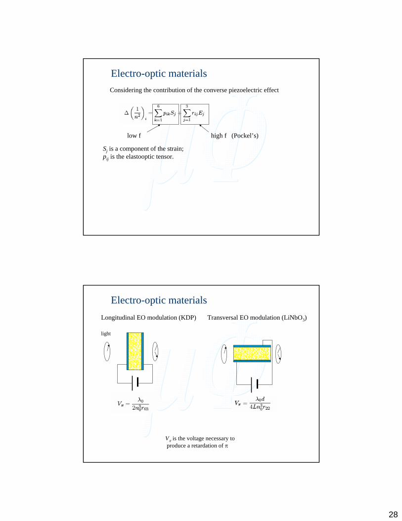
Electro-optic materialsConsidering the contribution of the converse piezoelectric effect
Sj is a component of the strain; pij is the elastooptic tensor.
low f high f (Pockel’s)
Electro-optic materialsLongitudinal EO modulation (KDP)
Vπ is the voltage necessary toproduce a retardation of π
Transversal EO modulation (LiNbO3)
light
29
Photorefractive materials
* With the kind contribution of Paul Muralt, EPFL, Lausanne CH
Photorefractive materials
Photorefractive materials are electroopticmaterials which exhibit also a high internal photovoltaic effect. They can be used to:
– Holographic storage

30
5 mm
LiNbO3:Fe
less Fe2+ more Fe2+
K. Buse et al., Phys. Rev. B 56, 1225 (1997)
CB
VB
hν
Fe 2+ Fe 3+
Photorefractive materials LiNbO3:Fe
)(32 CondBandeFehFe +↔+ ++ ν
iijjj Ernn 3
21
=∆
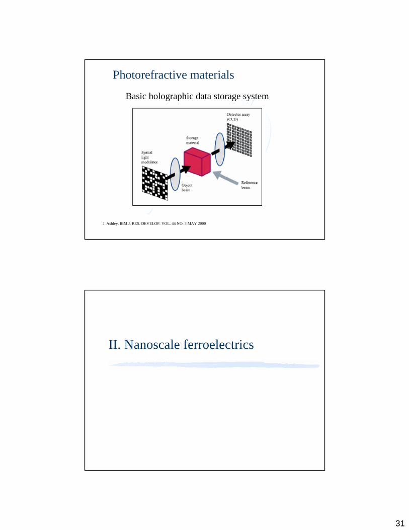
Photorefractive materialsHolographic storage
J. Ashley, IBM J. RES. DEVELOP. VOL. 44 NO. 3 MAY 2000
write read
31
Photorefractive materials
J. Ashley, IBM J. RES. DEVELOP. VOL. 44 NO. 3 MAY 2000
Basic holographic data storage system
II. Nanoscale ferroelectrics
32
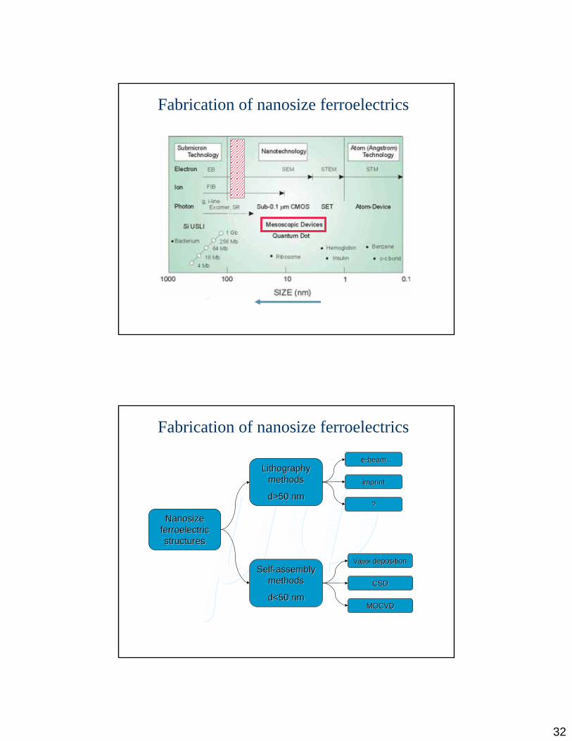
Fabrication of nanosize ferroelectrics
Fabrication of nanosize ferroelectrics
Nanosize Nanosize ferroelectric ferroelectric structuresstructures
Lithography Lithography methodsmethods
d>50 nmd>50 nm
SelfSelf--assembly assembly methodsmethods
d<50 nmd<50 nm
Vapor Vapor depositiondeposition
CSDCSD
MOCVDMOCVD
ee--beambeam
imprintimprint
??

33
Lithography
Maskless patterning methods
Ion-beam milling
34
Fabrication of nanosize ferroelectrics
(a)
(b)
(c) (d)
(e) (f)
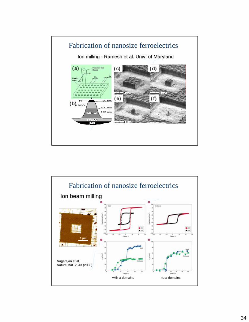
Ion milling Ion milling -- Ramesh et al. Univ. of MarylandRamesh et al. Univ. of Maryland
Fabrication of nanosize ferroelectricsIon beam millingIon beam milling
NagarajanNagarajan et al.et al.Nature Mat. 2, 43 (2003)Nature Mat. 2, 43 (2003)
1 µm
with awith a--domainsdomains no ano a--domainsdomains
35
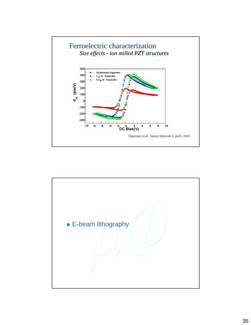
Ferroelectric characterizationSize effects Size effects -- ion milled PZT structuresion milled PZT structures
Nagarajan et al., Nature Materials 2, pp43, 2003
E-beam lithography
36
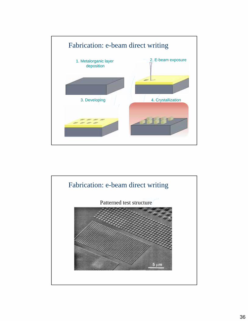
Fabrication: e-beam direct writing
1. Metalorganic layer 1. Metalorganic layer depositiondeposition
2. E2. E--beam exposurebeam exposure
4. Crystallization4. Crystallization3. Developing 3. Developing
Fabrication: e-beam direct writing
Patterned test structure
37
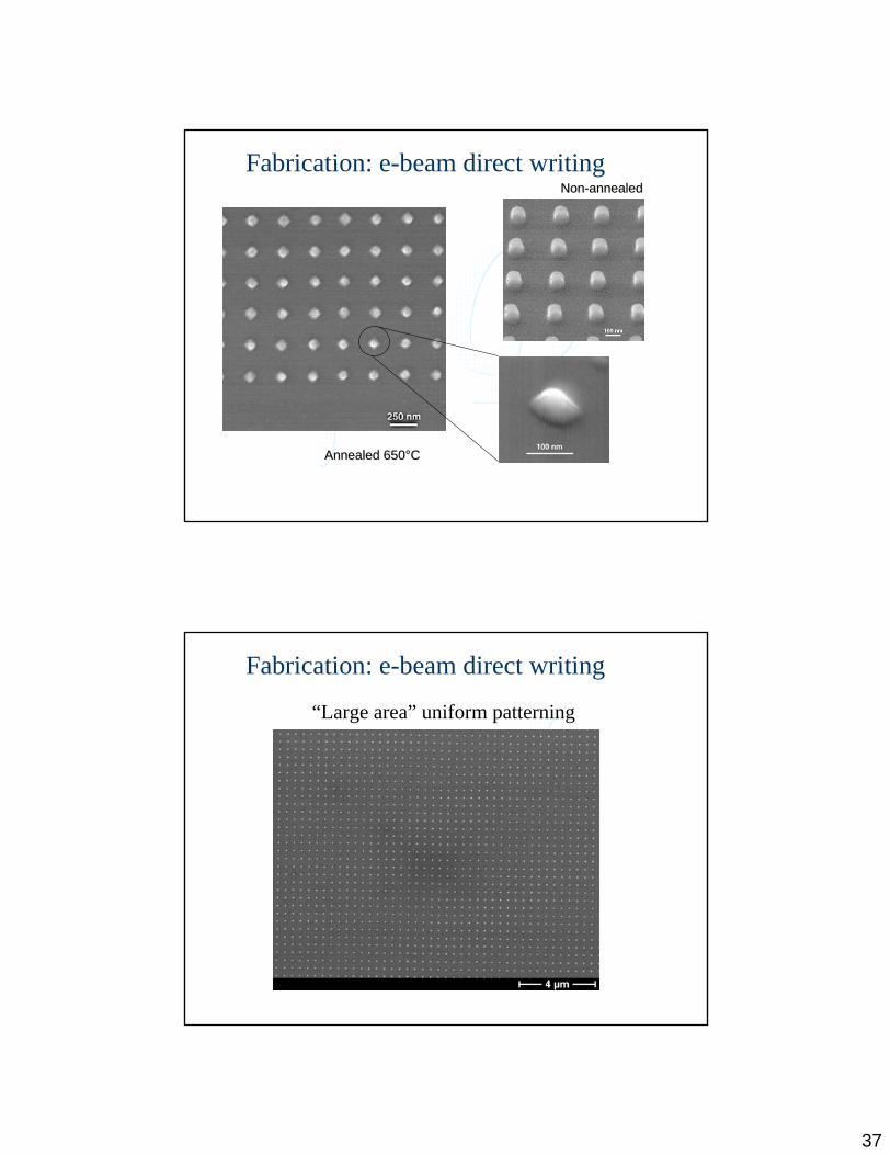
Fabrication: e-beam direct writing
Annealed 650°CAnnealed 650°C
NonNon--annealedannealed
Fabrication: e-beam direct writing
“Large area” uniform patterning
38
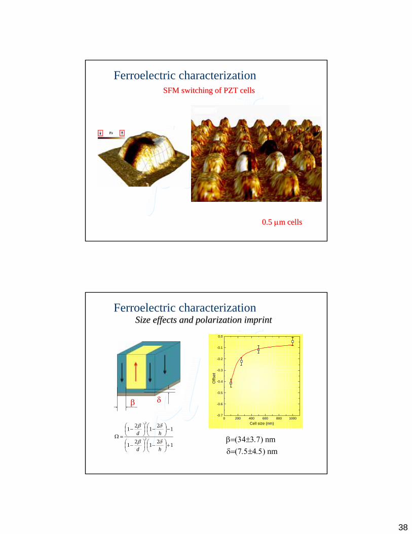
Ferroelectric characterizationSFM switching of PZT cellsSFM switching of PZT cells
0.50.5 µµm cellsm cells
Ferroelectric characterizationSize effects and polarization imprintSize effects and polarization imprint
0 200 400 600 800 1000-0.7
-0.6
-0.5
-0.4
-0.3
-0.2
-0.1
0.0
Offs
et
Cell size (nm)
ββ δδ
β=(34±3.7) nmδ=(7.5±4.5) nm
12121
12121
2
2
+⎟⎠⎞
⎜⎝⎛ −⎟
⎠⎞
⎜⎝⎛ −
−⎟⎠⎞
⎜⎝⎛ −⎟
⎠⎞
⎜⎝⎛ −
=Ω
hd
hdδβ
δβ
39
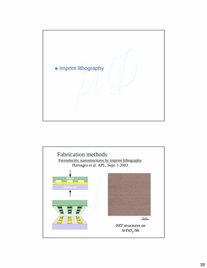
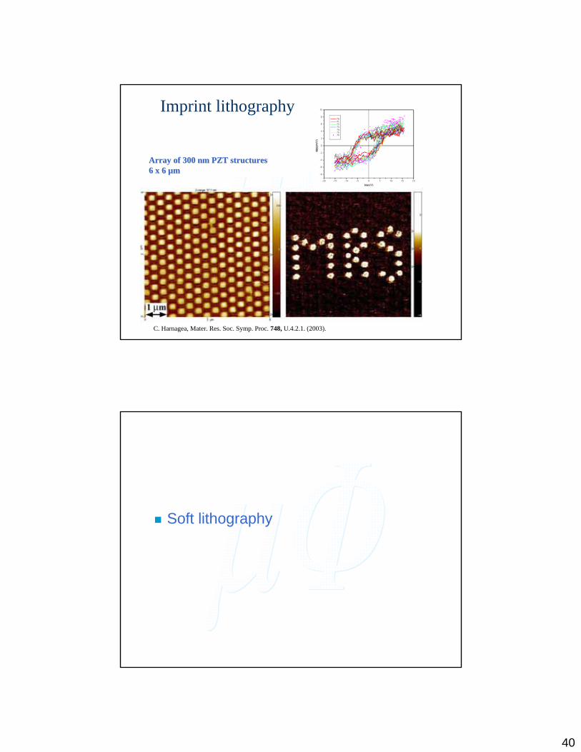
Imprint lithography
Fabrication methodsFerroelectric nanostructures by imprint lithography
Harnagea et al. APL, Sept. 1 2003
PZT structures on PZT structures on SrTiOSrTiO33:Nb:Nb
40
Array of 300 nm PZT structuresArray of 300 nm PZT structures6 x 6 µm6 x 6 µm
Imprint lithography
C. Harnagea, Mater. Res. Soc. Symp. Proc. 748, U.4.2.1. (2003).
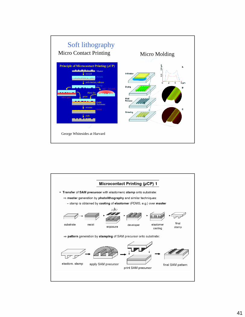
Soft lithography
41
Soft lithographyMicro Contact Printing Micro Molding
George Whitesides at Harvard
42
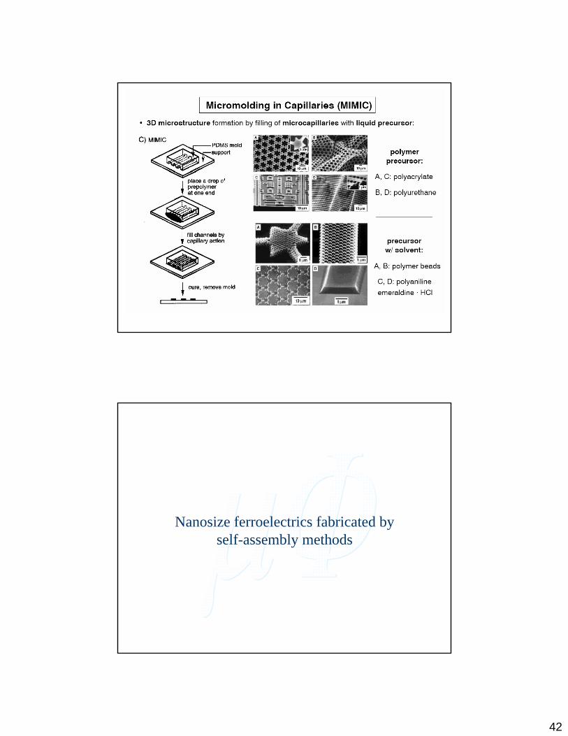
Nanosize ferroelectrics fabricated by self-assembly methods
43
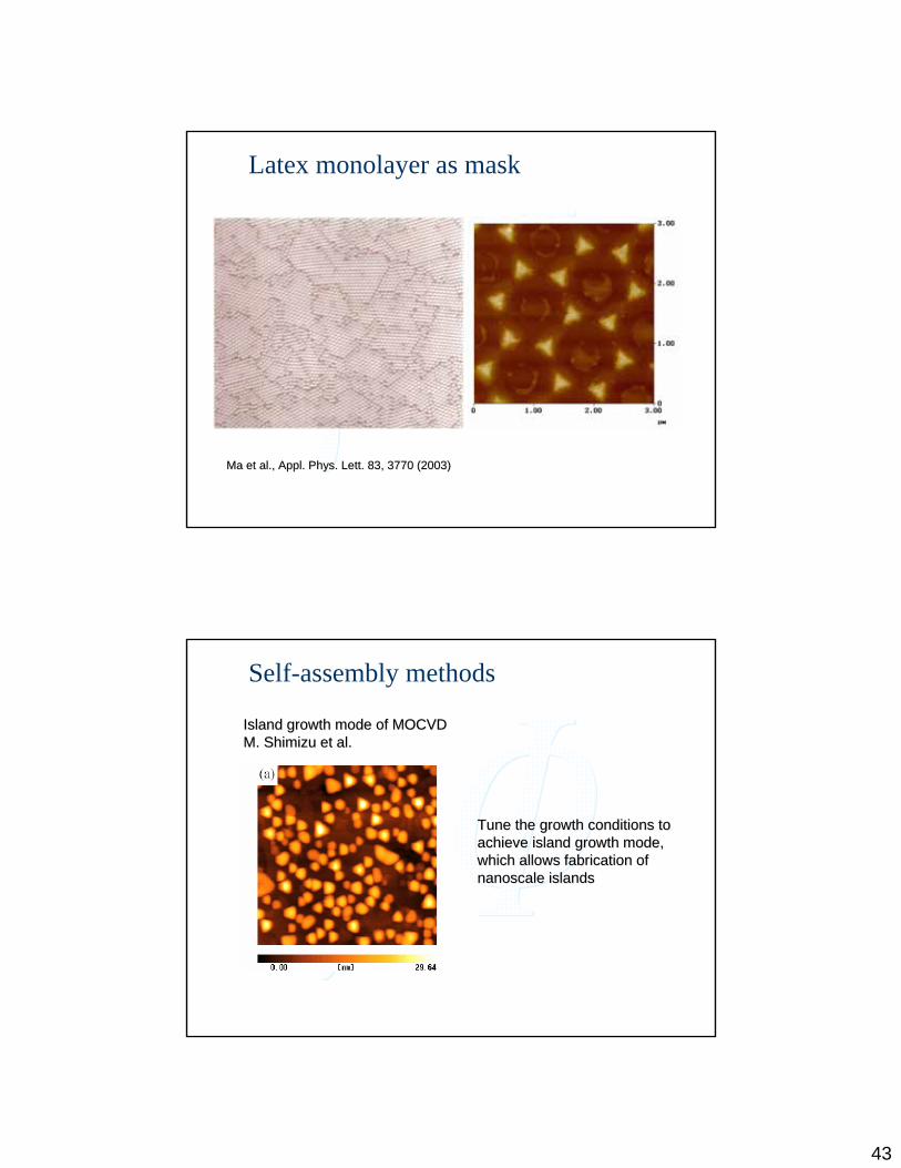
Latex monolayer as mask
Ma et al., Appl. Phys. Lett. 83, 3770 (2003)Ma et al., Appl. Phys. Lett. 83, 3770 (2003)
Self-assembly methods
Island growth mode of MOCVDIsland growth mode of MOCVDM. Shimizu et al.M. Shimizu et al.
Tune the growth conditions to Tune the growth conditions to achieve island growth mode, achieve island growth mode, which allows fabrication of which allows fabrication of nanoscale islands nanoscale islands
44
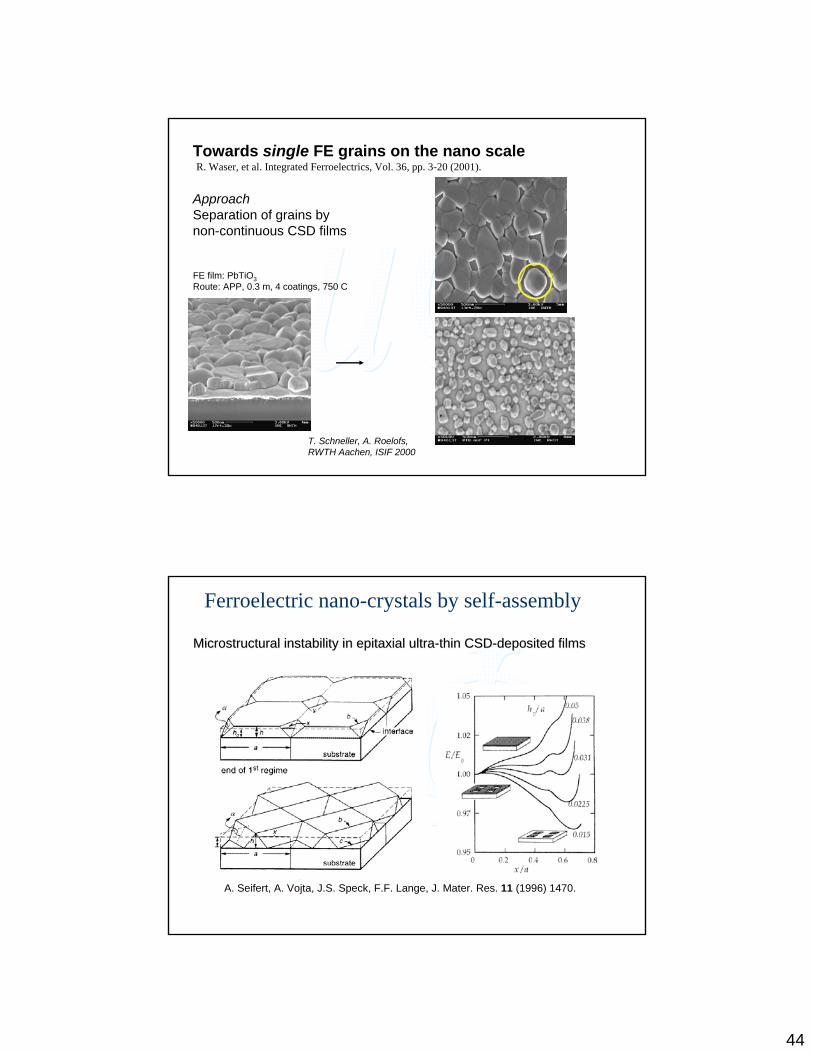
Towards single FE grains on the nano scale
T. Schneller, A. Roelofs, RWTH Aachen, ISIF 2000
ApproachSeparation of grains bynon-continuous CSD films
FE film: PbTiO3Route: APP, 0.3 m, 4 coatings, 750 C
R. Waser, et al. Integrated Ferroelectrics, Vol. 36, pp. 3-20 (2001).
A. Seifert, A. Vojta, J.S. Speck, F.F. Lange, J. Mater. Res. 11 (1996) 1470.
Ferroelectric nano-crystals by self-assembly
Microstructural instability in epitaxial ultraMicrostructural instability in epitaxial ultra--thin CSDthin CSD--deposited films deposited films
45
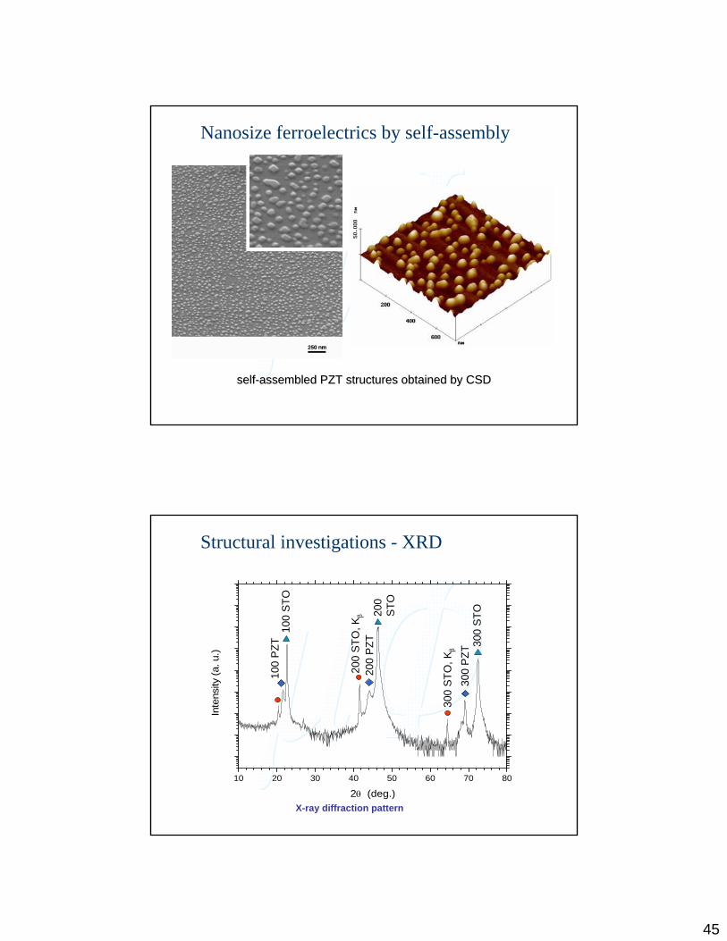
Nanosize ferroelectrics by self-assembly
selfself--assembled PZT structures obtained by CSDassembled PZT structures obtained by CSD
X-ray diffraction pattern
10 20 30 40 50 60 70 80
Inte
nsity
(a. u
.)
2θ (deg.)
100
STO
300
STO20
0S
TO
300
PZT
200
PZT
100
PZT
200
STO
, Kβ
300
STO
, Kβ
Structural investigations - XRD
46
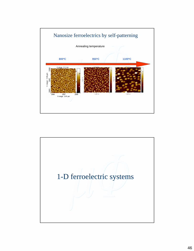
Annealing temperature
Nanosize ferroelectrics by self-patterning
800oC 950oC 1100oC
1-D ferroelectric systems

47
Nanowires
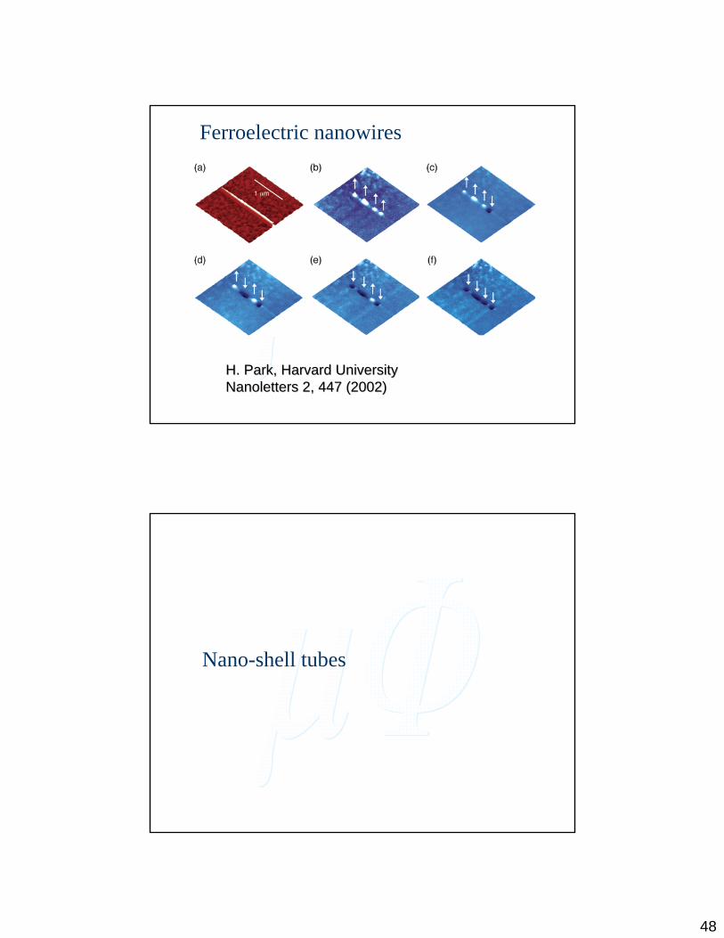
Ferroelectric nanowires
H. Park, Harvard UniversityNanoletters 2, 447 (2002)
48
Ferroelectric nanowires
H. Park, Harvard UniversityH. Park, Harvard UniversityNanolettersNanoletters 2, 447 (2002)2, 447 (2002)
Nano-shell tubes
49
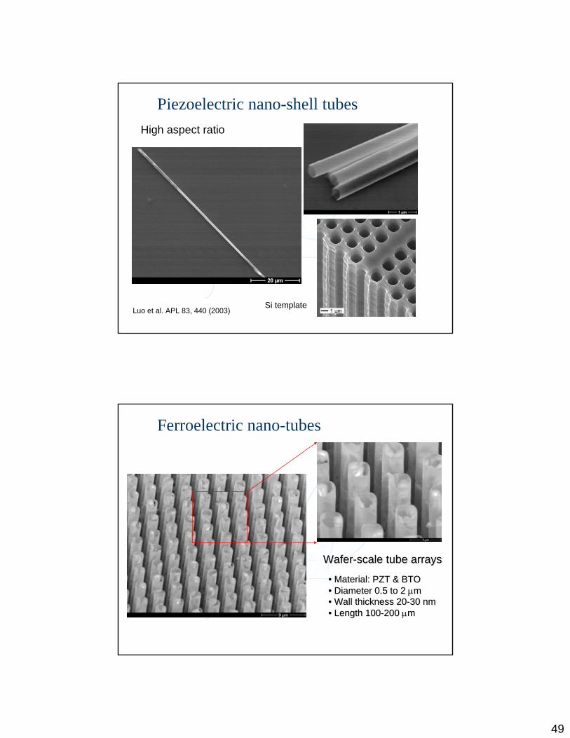
Piezoelectric nano-shell tubesHigh aspect ratio
Si templateLuo et al. APL 83, 440 (2003)
Ferroelectric nano-tubes
•• Material: PZT & BTOMaterial: PZT & BTO•• Diameter 0.5 to 2 Diameter 0.5 to 2 µµmm•• Wall thickness 20Wall thickness 20--30 nm30 nm•• Length 100Length 100--200 200 µµmm
WaferWafer--scale tube arraysscale tube arrays
50
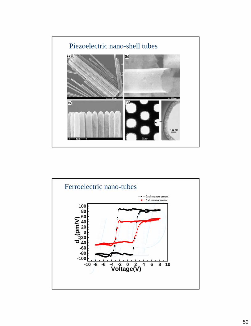
Piezoelectric nano-shell tubes
-10 -8 -6 -4 -2 0 2 4 6 8 10-100
-80-60-40-20
020406080
100
2nd measurement 1st measurement
d 33(p
m/V
)
Voltage(V)
Ferroelectric nano-tubes
51
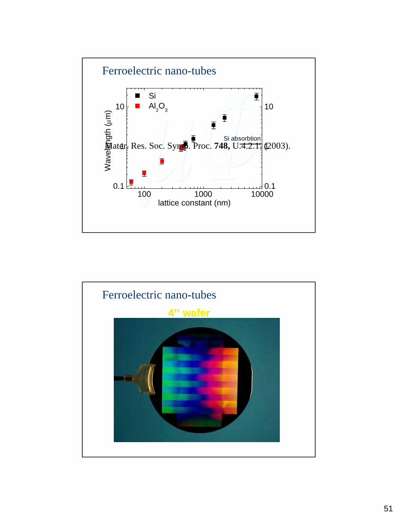
Ferroelectric nano-tubes
100 1000 100000.1
1
10
0.1
1
10
Si absorbtion
Wav
elen
gth
(µm
)
lattice constant (nm)
Si Al2O3
Mater. Res. Soc. Symp. Proc. 748, U.4.2.1. (2003).
Ferroelectric nano-tubes4’’ wafer4’’ wafer


![Piezoelectric, impedance, electric modulus and AC ... · 82 A.K. Roy et al. / Processing and Application of Ceramics 7 [2] (2013) 81–91 around which optimal piezoelectric and ferroelectric](https://static.fdocuments.in/doc/165x107/5bc9938609d3f2aa798cc6af/piezoelectric-impedance-electric-modulus-and-ac-82-ak-roy-et-al-processing.jpg)