FERROELECTRIC AND ANTIFERROELECTRIC PROPERTIES OF …
209
FERROELECTRIC AND ANTIFERROELECTRIC PROPERTIES OF HfO2-BASED THIN FILMS By PATRICK DOMINIC LOMENZO A DISSERTATION PRESENTED TO THE GRADUATE SCHOOL OF THE UNIVERSITY OF FLORIDA IN PARTIAL FULFILLMENT OF THE REQUIREMENTS FOR THE DEGREE OF DOCTOR OF PHILOSOPHY UNIVERSITY OF FLORIDA 2016
Transcript of FERROELECTRIC AND ANTIFERROELECTRIC PROPERTIES OF …
FERROELECTRIC AND ANTIFERROELECTRIC PROPERTIES OF HfO2-BASED THIN FILMS
By
PATRICK DOMINIC LOMENZO
A DISSERTATION PRESENTED TO THE GRADUATE SCHOOL OF THE UNIVERSITY OF FLORIDA IN PARTIAL FULFILLMENT
OF THE REQUIREMENTS FOR THE DEGREE OF DOCTOR OF PHILOSOPHY
UNIVERSITY OF FLORIDA
2016

© 2016 Patrick D. Lomenzo

3
ACKNOWLEDGMENTS
I would like to acknowledge Dr. Nishida, my PhD advisor, for his encouragement,
openness to new ideas, and his constant support throughout my time as a PhD student
at the University of Florida. Under Dr. Nishida’s guidance, I learned an immense amount
of technical and non-technical skills which will continue to aid me in the future. I thank
all of my PhD committee members for their interest and support: Dr. Y.K. Yoon, Dr. Jing
Guo, and Dr. Brent Gila.
I would like to acknowledge the Nanoscale Research Facility (NRF) staff for all of
their help throughout my program. Discussions with David Hays and Bill Lewis always
made me walk away with a greater understanding of the fabrication equipment I was
using. Andres Trucco was invaluable in helping me run the ALD tool and solving
problems we encountered along the way. I would especially like to thank Brent Gila who
kept the Nanoscale Research Facility running efficiently and in a user-friendly manner.
Dr. Gila’s help in developing ALD recipes and his willingness to expand the capabilities
of various tools helped make my project a success.
I would also like to thank Qanit Takmeel for his help in fabrication as well as Dr.
Saeed Moghaddam. Dr. Jacob Jones is acknowledged for helping us analyze and better
understand the material properties of the HfO2 thin films which led to many productive
collaborations. I would like to thank Sean McLaughlin for his support of the HfO2 project,
I had many good discussions with Sean and his team at Northrop Grumman. I would
also like to thank all of my colleagues at IMG, it has been a rewarding experience
working with such a great group of people. I would also like to thank the Semiconductor
Research Corporation (SRC) for awarding me a fellowship that supported me during my
time as a PhD student.

4
TABLE OF CONTENTS page
ACKNOWLEDGMENTS .................................................................................................. 3
LIST OF TABLES ............................................................................................................ 7
LIST OF FIGURES .......................................................................................................... 8
LIST OF ABBREVIATIONS ........................................................................................... 14
ABSTRACT ................................................................................................................... 15
CHAPTER
1 INTRODUCTION .................................................................................................... 17
1.1 Properties of Ferroelectrics ............................................................................... 17
1.2 Dissertation Organization .................................................................................. 25
2 HAFNIUM OXIDE: BULK AND THIN FILM PROPERTIES ..................................... 29
2.1 Background ....................................................................................................... 29
2.2 Properties of Bulk HfO2 ..................................................................................... 30 2.3 HfO2 Thin Film Properties ................................................................................. 33
2.3.1 HfO2 as a High-K Gate Material ............................................................... 33
2.3.2 Enhancing the Dielectric Constant of HfO2 .............................................. 36
2.4 Ferroelectricity in HfO2-Based Thin Films ......................................................... 39 2.5 Applications for Ferroelectric and Antiferroelectric HfO2 ................................... 47
3 MEASUREMENT METHODS AND TECHNIQUES ................................................ 56
3.1 Background ....................................................................................................... 56 3.2 Electrical Measurements and Techniques ........................................................ 57
3.2.1 Hysteresis Loops ..................................................................................... 57 3.2.2 Dynamic Hysteresis Currents .................................................................. 61 3.2.3 Positive-Up-Negative-Down (PUND) ....................................................... 64
3.2.4 Capacitance-Voltage (CV) ....................................................................... 67 3.2.5 Endurance Cycling .................................................................................. 69
3.2.6 Retention Tests ....................................................................................... 73 3.2.7 Impedance Spectroscopy ........................................................................ 75
3.3 Materials Characterization Techniques ............................................................. 78 3.3.1 X-ray Photoelectron Spectroscopy (XPS) ................................................ 78 3.3.2 Time-of-Flight Secondary Ion Mass Spectrometry (TOF-SIMS) .............. 80 3.3.3 Grazing Incidence X-ray Diffraction (GI-XRD) ......................................... 82 3.3.4 Transmission Electron Microscopy (TEM) ............................................... 83

5
4 FERROELECTRIC PHENOMENA IN Si-DOPED HfO2 THIN FILMS WITH TiN AND Ir ELECTRODES ............................................................................................ 84
4.1 Background ....................................................................................................... 84
4.2 Experiment ........................................................................................................ 87 4.3 Results and Discussion ..................................................................................... 89 4.4 Conclusion ...................................................................................................... 102
5 THE EFFECTS OF LAYERING IN FERROELECTRIC Si-DOPED HfO2 THIN FILMS ................................................................................................................... 104
5.1 Background ..................................................................................................... 104 5.2 Experiment ...................................................................................................... 106
5.3 Results ............................................................................................................ 108 5.4 Conclusion ...................................................................................................... 114
6 TaN INTERFACE PROPERTIES AND ELECTRIC FIELD CYCLING EFFECTS IN Si-DOPED HfO2 THIN FILMS ........................................................................... 116
6.1 Background ..................................................................................................... 116 6.2 Experiment ...................................................................................................... 119
6.3 Results and Discussion ................................................................................... 122 6.4 Conclusion ...................................................................................................... 138
7 FERROELECTRIC Si-DOPED DEVICES PROPERTIES ON HIGHLY DOPED GERMANIUM ....................................................................................................... 141
7.1 Background ..................................................................................................... 141
7.2 Experiment ...................................................................................................... 142 7.3 Results and Discussion ................................................................................... 143
7.4 Conclusion ...................................................................................................... 146
8 MIXED Al AND Si DOPING IN FERROELECTRIC HfO2 THIN FILMS ................. 148
8.1 Background ..................................................................................................... 148
8.2 Experiment ...................................................................................................... 149 8.3 Results and Discussion ................................................................................... 151 8.4 Conclusion ...................................................................................................... 157
9 ANNEALING BEHAVIOR OF FERROELECTRIC Si-DOPED HfO2 THIN FILMS . 158
9.1 Background ..................................................................................................... 158 9.2 Experiment ...................................................................................................... 160 9.3 Results and Discussion ................................................................................... 161 9.4 Conclusion ...................................................................................................... 171
10 STUDIES ON FERROELECTRIC AND ANTIFERROELECTRIC HAFNIUM-ZIRCONIUM OXIDE-BASED THIN FILMS ........................................................... 173

6
10.1 Background ................................................................................................... 173 10.2 Experiment .................................................................................................... 175 10.3 Influence of Doping Hf0.5Zr0.5O2 with Al or Si ................................................ 176
10.4 Thickness Dependence of Ferroelectric Hf0.5Zr0.5O2 ..................................... 182 10.5 Compositionally Graded HfxZr1-xO2 Thin Films .............................................. 187 10.6 Conclusion .................................................................................................... 192
11 SUMMARY AND FUTURE WORK ....................................................................... 194
APPENDIX
A: PROCESS FLOW FOR FERROELECTRIC HfO2 CAPACITORS ......................... 196
B: DESCRIPTION OF ATOMIC LAYER DEPOSITION PROCESS ........................... 197
LIST OF REFERENCES ............................................................................................. 200
BIOGRAPHICAL SKETCH .......................................................................................... 209

7
LIST OF TABLES
Table page 2-1 Conventional nonvolatile memory technologies compared with FRAM. ............. 49
2-2 Comparison of emerging alternative nonvolatile memory technologies. ............. 52
6-1 Acceleration factors for the Si-doped HfO2 thin films. ....................................... 125
B-1 List of ALD precursors and the materials grown. .............................................. 198
B-2 ALD recipe specifications. ................................................................................ 199

8
LIST OF FIGURES
Figure page 1-1 In a linear dielectric or cubic crystal, an electric field is required to induce a
dipole moment in which the distortion of the electron cloud around the nuclei of the atoms produces polarization. .................................................................... 19
1-2 For ferroelectric lead titanate, the tetragonal lattice cell is noncentrosymmetric and the displacement of the central Ti cation with respect to the oxygen anions dictates the polarization direction. ........................ 20
1-3 A single crystal ferroelectric has a square polarization vs. electric field profile, whereas the polycrystalline ferroelectric is slanted. ............................................ 22
1-4 While as-grown ferroelectrics have a random alignment of ferroelectric domain orientations, electrically poling ferroelectrics can induce a preferred polarization direction in both single crystals and polycrystalline materials. ......... 22
1-5 Ferroelastic switching occurs when a-domains 90 ° switch to c-domains, whereas 180 ° switching occurs during conventional polarization reversal with the application of an electric field. ............................................................... 23
1-6 Aberration corrected STEM is used to map out the dipole orientations and domain walls in PTO. .......................................................................................... 24
2-1 Phase diagram of the HfxZr1-xO2 solid solution system. ...................................... 31
2-2 Phase diagram of HfO2 with temperature and pressure. .................................... 32
2-3 Unit lattice cells of some crystal phases of HfO2 and ZrO2. Large atoms are the metal cations and small atoms are the oxygen anions. ................................ 32
2-4 Breakdown field and bandgap of various high-k materials plotted against the dielectric constant. .............................................................................................. 34
2-5 Direct and indirect scavenging techniques. ........................................................ 35
2-6 PMOS and NMOS transistor structures for Intel’s 22 nm node........................... 36
2-7 The measured dielectric constant of Hf1-xSixO2 as a function of Si concentration. ..................................................................................................... 38
2-8 Atomic force microscopy scans of HfO2 thin films annealed at 1000 °C with and without a TiN electrode. ............................................................................... 39

9
2-9 The Si-doped HfO2 thin film which is capped with a TiN electrode during a crystallization anneal led to a strong orthorhombic or tetragonal diffraction signal. ................................................................................................................. 40
2-10 Hysteresis and piezoelectric displacement curves illustrate how Si doping can lead to ferroelectric and antiferroelectric-like characteristics........................ 41
2-11 The hysteresis and relative permittivity indicates a paraelectric to ferroelectric phase transition as the composition of HfO2 is modified with Zr until a Hf0.5Zr0.5O2 film composition is reached. ............................................................. 42
2-12 The 2Pr and relative phase fraction of Hf0.5Zr0.5O2 films from 5.5 nm to 25 nm thick as a function of anneal temperature. .......................................................... 44
2-13 Different crystal phases of hafnium oxide. .......................................................... 46
2-14 STEM is used to identify the polar orthorhombic phase. .................................... 47
2-15 Two different forms of the FRAM memory cell.................................................... 49
2-16 Process flow and cross-sectional image of 3D trench capacitors incorporating Al-doped HfO2 are shown along with the equivalent planar area hysteresis measurement. ..................................................................................................... 51
3-1 An implementation of the Sawyer-Tower used to extract the hysteresis plots of ferroelectric capacitors. .................................................................................. 57
3-2 A hysteresis plot allows the extraction of several important ferroelectric parameters. ........................................................................................................ 59
3-3 The energy storage density and loss of an antiferroelectric capacitor can be determined by integrating regions within the hysteresis plot. ............................. 61
3-4 Modified Sawyer-Tower circuit for dynamic hysteresis current measurements. . 62
3-5 Dynamic hysteresis current measurements. ....................................................... 63
3-6 PUND waveform and measurement circuit. ........................................................ 64
3-7 The PUND waveform is applied to a ferroelectric thin film. ................................. 66
3-8 C-V characteristics of ferroelectric thin films. ...................................................... 68
3-9 Bipolar square waves are used to cycle ferroelectric capacitors. ....................... 70
3-10 Fatigue occurs in these ferroelectric Al/Si-doped HfO2 thin films from 104 to 108 cycles. .......................................................................................................... 72

10
3-11 Retention tests are performed by baking ferroelectric capacitors in a polarization state and delivering pulse trains to measure data retention. ........... 74
3-12 The Ti 2p binding energy spectra show that Ti is chemically bonded in the forms of TiO2, Ti2O3, TiN, and TiC on the surface of an ALD TiN film. ............... 79
3-13 Depth profile obtained with XPS of ALD grown TiN electrodes. ......................... 80
3-14 TOF-SIMS profile of a TaN/Si-doped HfO2/TaN capacitor where the Si concentration has been quantified and relative count yields for the other elements are given. ............................................................................................ 82
3-15 TEM is used to confirm the thickness and crystallinity of Hf0.5Zr0.5O2 after ALD growth at 400 °C. ........................................................................................ 83
4-1 Growth of the HfO2/SiO2 interfacial layer and the expansion of the TiN electrode can be seen when compared to the as-deposited film. ....................... 89
4-2 Electrical and ferroelectric characterization of TiN MFIS devices after different annealing conditions. ............................................................................ 91
4-3 Electrical and ferroelectric characterization of Ir MFIS devices after different annealing conditions. .......................................................................................... 92
4-4 Comparison of HF surface treatment vs. native SiO2. ........................................ 94
4-5 HAADF STEM images of Ir and TiN MFIS stacks.. ............................................. 95
4-6 Hysteresis of TiN and Ir capped MFIS devices different anneals. ...................... 96
4-7 Hysteresis of MFIS HfO2 capacitors with varying Si-doping concentrations. ...... 98
4-8 GIXRD of the Ir and TiN capped HfO2 films with different doping concentrations are shown with the theoretical peak positions of the orthorhombic, tetragonal, and monoclinic phases of HfO2. ................................. 99
4-9 Ferroelectric and capacitance characteristics of MFM device with Ir electrodes annealed at 1000 °C for 1 s. ........................................................... 101
5-1 Hysteresis dependence on Si layering. ............................................................ 110
5-2 Changing the Si concentration and the ALD cycle ratio both show changes in the hysteresis characteristics............................................................................ 111
5-3 Cross-sectional HAADF STEM images of the Ir/HfO2:SiO2/Si-stacked samples. ........................................................................................................... 112
5-4 Cycling characteristics of layered Si-doped HfO2 thin films.. ............................ 113

11
6-1 Hysteresis of the 1.2 mol. % Si films with sputtered TaN electrodes. ............... 124
6-2 The change in the remanent polarization with cycling. ..................................... 125
6-3 GIXRD of the Si-doped HfO2 thin films shows the crystal structure to be consistent with the tetragonal or orthorhombic phase for both compositions. .. 126
6-4 XPS analysis of the TE interface. ..................................................................... 128
6-5 As-grown ferroelectric domains are preferentially polarized upward toward the top electrode in the Si-doped HfO2 thin films. ............................................. 130
6-6 TEM confirms the presence of a ~ 1 nm TaxOy layer at the TaN BE interface. . 131
6-7 Switching properties of the Si-doped HfO2 thin films with TaN electrodes. ....... 133
6-8 Switching kinetics and switching current of 1.6 mol. % Si doped HfO2 thin film with a lower anneal temperature. ...................................................................... 137
7-1 HRTEM cross-sectional images of different device stacks. .............................. 144
7-2 Ferroelectric characteristics of Si-doped HfO2 on Ge. ...................................... 144
7-3 Grazing incidence x-ray diffraction shows that the Si-doped HfO2 thin films are consistent with the tetragonal or Pca21 orthorhombic phase. ..................... 145
7-4 Switching characteristics of ferroelectric SI-doped HfO2 on Ge. ....................... 146
8-1 Hysteresis characteristics of the mixed Al and Si doped HfO2 thin films........... 152
8-2 GIXRD confirms the possible existence of the orthorhombic Pca21 phase in all three of the Al and Si doped HfO2 thin films annealed at 800 °C. ................ 154
8-3 TOF-SIMS depth profiles of the mixed Al and Si-doped HfO2 thin films. .......... 155
8-4 HR-TEM image of the Si-Al-Al-Si doped HfO2 thin film after annealing at 850 °C. Lattice fringes can be seen in the polycrystalline TiN electrodes................ 155
8-5 Anneal temperature dependence of the mixed Al and Si-doped HfO2 thin films. ................................................................................................................. 156
9-1 The virgin hysteresis characteristics of the 24:1 and 16:1 HfO2:SiO2 thin films show an antiferroelectric-like to ferroelectric transition for increasing anneal temperature. ..................................................................................................... 162
9-2 The relative permittivity of the virgin 24:1 HfO2:SiO2 captures the antiferroelectric-like to ferroelectric transition which occurs with increasing anneal temperature. ......................................................................................... 163

12
9-3 Electrical and ferroelectric parameters of Si-doped HfO2 with anneal temperature. ..................................................................................................... 164
9-4 Ferroelectric and electrical properties of Si-doped HfO2 with anneal time. ...... 167
9-5 Three unique cases demonstrating the effects of electric field cycling in the Si-doped HfO2 thin films. .................................................................................. 169
10-1 Hysteresis and dynamic hysteresis currents with cycling for HZO films ........... 177
10-2 Energy storage density and efficiency of Al or Si-doped Hf0.5Zr0.5O2 thin films with anneal temperature. .................................................................................. 180
10-3 Energy storage density and efficiency of Al or Si-doped Hf0.5Zr0.5O2 thin films with cycling. ...................................................................................................... 181
10-4 Reliability of Si-doped Hf0.5Zr0.5O2 with cycling at elevated temperature. ......... 182
10-5 Reliability of Al-doped Hf0.5Zr0.5O2 with cycling at elevated temperature. ......... 182
10-6 Hysteresis characteristics of Hf0.5Zr0.5O2 thin films from 15 nm – 6 nm in thickness with different anneal temperatures. .................................................. 183
10-7 The remanent polarization of the Hf0.5Zr0.5O2 films with thickness and anneal temperature, before and after cycling at 1 kHz. ................................................ 184
10-8 The relative permittivity vs. electric field curves show that most of the films have secondary high-field shoulders which disappear after cycling, except in the case of the 6 nm thick Hf0.5Zr0.5O2 films. ..................................................... 185
10-9 Retention characteristics of 10 nm Hf0.5Zr0.5O2 films before and after cycling at 1 kHz. ........................................................................................................... 185
10-10 Retention tests carried out on 15, 10, and 6 nm thick Hf0.5Zr0.5O2 films after cycling at 1 kHz. ............................................................................................... 186
10-11 Imprint shifts are shown in red and blue for positive and negative state bakes respectively....................................................................................................... 187
10-12 Hysteresis characteristics of Hf0.5Zr0.5O2 thin films with a Hf-rich center at different thicknesses and anneal temperatures. ............................................... 188
10-13 Hysteresis characteristics of HfxZr1-xO2 thin films with a Hf-rich center and Zr-rich ends at different thicknesses and anneal temperatures. ............................ 189
10-14 The retention characteristics of the HRC films at 6 nm shows an increase in the polarization margin with higher electric fields. ............................................ 190
13
10-15 Inverse capacitance with film thickness for binary Hf0.5Zr0.5O2, HRC, and ZRE films. ................................................................................................................. 191
B-1 Flow diagram of an ALD recipe. ....................................................................... 198

14
LIST OF ABBREVIATIONS
CMOS Complementary Metal Oxide Semiconductor
DRAM Dynamic Random Access Memory
Ec Coercive Field
EIB Internal Bias Field
ESD Energy Storage Density
FeFET Ferroelectric Field Effect Transistor
FRAM Ferroelectric Random Access Memory
FTJ Ferroelectric Tunnel Junction
HZO HfxZr1-xO2
MFIS Metal Ferroelectric Insulator Semiconductor
MFM Metal Ferroelectric Metal
MFS Metal Ferroelectric Semiconductor
NVM Nonvolatile Memory
P Polarization
Pr Remanent Polarization
Ps Spontaneous Polarization
Psw Switched Polarization
RTA Rapid Thermal Anneal
Vc Coercive Voltage

15
Abstract of Dissertation Presented to the Graduate School of the University of Florida in Partial Fulfillment of the Requirements for the Degree of Doctor of Philosophy
FERROELECTRIC AND ANTIFERROELECTRIC PROPERTIES OF HfO2-BASED THIN
FILMS
By
Patrick D. Lomenzo
May 2016
Chair: Toshikazu Nishida Major: Electrical and Computer Engineering
Ferroelectric HfO2-based thin films are attractive candidates for nonvolatile
memories technologies such as ferroelectric random access memory (FRAM) and
ferroelectric field effect transistors (FeFETs). Conventional perovskite ferroelectric
memories have been unable to scale to high densities and are not CMOS compatible,
which has prevented ferroelectric-based memory technologies from being widely
adopted despite their low read/write power, high read/write speeds, and impressive
cycling properties. Ferroelectric HfO2 thin films can overcome the integration hurdles
associated with perovskite ferroelectrics because HfO2 can be deposited through
conformal atomic layer deposition (ALD), exhibit ferroelectric properties down to 5nm
thicknesses, and are CMOS compatible.
A variety of processing techniques and devices were investigated to study the
ferroelectric behavior of HfO2 based thin films under different conditions. When dopants
such as Si and Al were incorporated into HfO2, mutually competing phase transitions
produced paraelectric, ferroelectric, or antiferroelectric characteristics. The overall
concentration of such dopants and the spatial distribution of the dopant layers was
shown to substantially impact ferroelectricity in HfO2. The fully miscible HfxZr1-xO2

16
composition was adjusted to produce a range of ferroelectric and antiferroelectric
properties. Layered concentration gradients of Hf and Zr within HfxZr1-xO2 thin films were
demonstrated to add further capabilities in the ability to engineer the electrical and
ferroelectric properties of HfO2-based thin films.
Extrinsic effects such as the device structure, the substrate and capping
electrode material, and defects, such as oxygen vacancies, were observed to influence
the overall behavior of ferroelectric HfO2-based thin films. Due to the ultra-thin
dimensions of HfO2-based ferroelectrics, interactions between the electrode and
ferroelectric interface were found to induce space charge effects and depolarization
fields. The overall reliability of HfO2-based ferroelectrics was heavily influenced by the
choice of electrode material, anneal temperature, and applied electric field.
Hf0.5Zr0.5O2 thin films doped with Al or Si exhibited antiferroelectric characteristics
in which reversible field-induced phase transitions took place. The large energy storage
density and high efficiency of antiferroelectric thin films make them exceptional
candidates for on-chip energy storage. Reliability tests at elevated temperature were
carried out to demonstrate the cycling characteristics of doped Hf0.5Zr0.5O2
antiferroelectrics and the data retention of HfO2-based ferroelectrics.

17
CHAPTER 1 INTRODUCTION
1.1 Properties of Ferroelectrics
The ability to retain a remanent polarization (Pr) in the absence of an electric field
gives a ferroelectric material the unique capability of harnessing its polarization state as
the basis for electronic memories. Ferroelectricity occurs in crystalline or polycrystalline
materials which have a polar, noncentrosymmetric crystal structure. Ferroelectrics can
be further defined as a pyroelectric material in which there are at least two
thermodynamically stable polarization states.1 Unlike linear dielectrics where a net
polarization produced by the distortion of the electron cloud and the nuclei of the atoms
vanishes when an applied electric field is removed, a relative displacement of anions
and cations within the unit lattice cell of a ferroelectric persists even without an electric
field. Due to the noncentrosymmetric lattice cell, the center of positive and negative
charge do not coincide and a spontaneous polarization (Ps) is produced as a result of
the ionic displacement within the unit cell. The remanent polarization remains stable
when the applied electric field is removed and can be reversed when the opposite
polarity of the electric field is applied.
In general, polarization (P) may be defined as the net dipole moment per unit
volume. The net dipole moment can be defined as2
nnrqP (1-1)
where qn is the charge and rn is the position vector of the charge. In the absence of an
external electric field, the net dipole moment of nonpolar systems is zero whereas polar
molecules and materials, H2O and ferroelectrics for example, will yield a finite net dipole
moment. The electric displacement field in free space is given by3

18
ED 0 (1-2)
where ε0 is the permittivity of free space and E is the electric field. For linear isotropic
dielectrics or cubic crystals, the polarization produced from the net dipole moment of the
electron cloud and atomic nuclei of the material must be added to Eq. 1-2
PED 0 . (1-3)
The polarization can be further defined as
EP e 0 (1-4)
where χe is the electric susceptibility of the material. The electric displacement field from
Eq. 1-3 can now be expressed as
EEEED ee 1000 (1-5)
where ε is the material permittivity. From Eq. 1-5, the relative permittivity is
er
1
0
. (1-6)
For anisotropic materials or non-cubic crystals, Eq. 1-5 and Eq. 1-6 must be rewritten
with the electric susceptibility and dielectric constant tensors4
jiji ED (1-7)
ijeijr ,, 1 . (1-8)
Figure 1-1 shows an illustration of the net dipole moment of a dielectric with and without
an applied electric field. The relative permittivity of a dielectric is important because it
determines the capacitance as shown by
d
AC r 0 (1-9)
where A is the electrode area and d is the dielectric film thickness.

19
Figure 1-1. In a linear dielectric or cubic crystal, an electric field is required to induce a dipole moment in which the distortion of the electron cloud around the nuclei of the atoms produces polarization.
In a ferroelectric, the application of an electric field displaces ions within the
noncentrosymmetric lattice cell and produces a dipole moment called the spontaneous
polarization. The spontaneous polarization term must now be included in Eq. 1-5
sse PEPEED 00 . (1-10)
The electric displacement field for ferroelectrics includes both the non-switching
dielectric term and the ferroelectric dipole switching term from the spontaneous
polarization.5
Figure 1-2 illustrates the polarization produced by the tetragonal lattice cell of a
common perovskite ferroelectric material, PbTiO3, known as lead titanate (PTO) which
is similar to Pb(ZrxTi1-x)O3 (PZT). In PTO, the displacement of the central cation with
respect to the oxygen anions shifts the positive and negative center of charge, thus
creating a dipole moment. If the oxygen anions shift more strongly in the same direction
as the central cation, then the polarization direction would be reversed in Figure 1-2
since the polarization vector begins at net negative charge and ends at net positive
charge.6 The change in direction of polarization, either up or down along the long c-axis
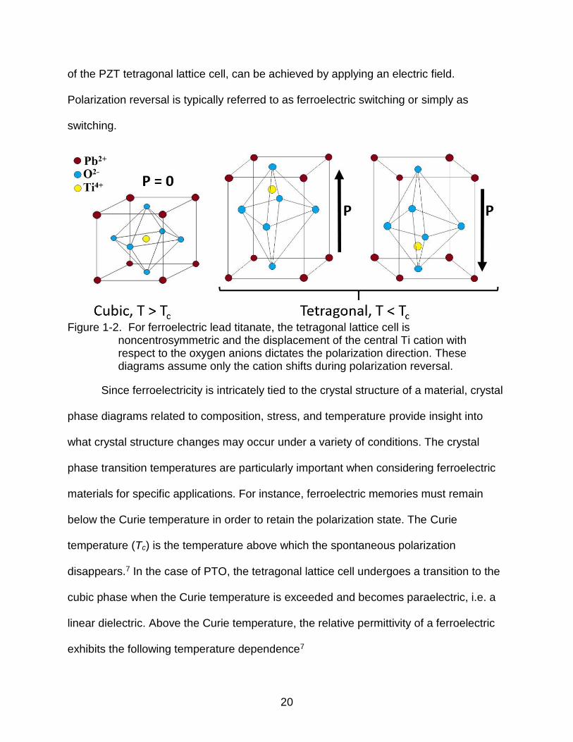
20
of the PZT tetragonal lattice cell, can be achieved by applying an electric field.
Polarization reversal is typically referred to as ferroelectric switching or simply as
switching.
Figure 1-2. For ferroelectric lead titanate, the tetragonal lattice cell is
noncentrosymmetric and the displacement of the central Ti cation with respect to the oxygen anions dictates the polarization direction. These diagrams assume only the cation shifts during polarization reversal.
Since ferroelectricity is intricately tied to the crystal structure of a material, crystal
phase diagrams related to composition, stress, and temperature provide insight into
what crystal structure changes may occur under a variety of conditions. The crystal
phase transition temperatures are particularly important when considering ferroelectric
materials for specific applications. For instance, ferroelectric memories must remain
below the Curie temperature in order to retain the polarization state. The Curie
temperature (Tc) is the temperature above which the spontaneous polarization
disappears.7 In the case of PTO, the tetragonal lattice cell undergoes a transition to the
cubic phase when the Curie temperature is exceeded and becomes paraelectric, i.e. a
linear dielectric. Above the Curie temperature, the relative permittivity of a ferroelectric
exhibits the following temperature dependence7

21
0TT
Cr
(1-11)
where C is the Curie constant, T is the temperature, and T0 is extracted from an
extrapolation of when the inverse relative permittivity intersects the temperature axis.
Ferroelectric materials may be single crystal or polycrystalline. Bulk ferroelectrics
may be single crystal depending on the growth conditions while thin film ferroelectrics
are typically polycrystalline. The switching properties of ferroelectrics can be strongly
influenced on whether the material is single crystal or polycrystalline. For instance, in a
single crystal, all of the ferroelectric dipoles switch uniformly and are aligned in the
same direction. However, for a polycrystalline ferroelectric, the dipoles are aggregated
into contiguous clusters called ferroelectric domains. Ferroelectric domains may have
different polarization orientations and switching characteristics; however, contiguous
lattice cells within a ferroelectric domain generally share the same polarization
orientation up to a domain wall boundary. Ferroelectric single crystals have a single
domain while polycrystalline ferroelectrics may have many domains. Figure 1-3
illustrates the typical differences in the polarization vs. electric field response between a
single crystal and a polycrystalline material.
Figure 1-4 illustrates a conceptual sketch of how domains may behave in
polycrystalline materials and single crystals. Barring extrinsic effects which can produce
internal electric fields, when ferroelectrics are grown, all of the domains have a random
polarization orientation and will yield a net zero polarization. Poling of a ferroelectric
encourages the ferroelectric domains to align in a direction parallel to the applied
electric field. A ferroelectric exposed to a DC electric field for a given period of time is
said to be poled.8 In single crystals, one domain will be oriented to the direction of the

22
electric field, while polycrystalline ferroelectrics will have some domains which align with
the electric field but will also have domains which have an in-plane polarization.
Ferroelectric dipoles which are polarized in the plane of the film do not participate in the
ferroelectric switching process that occurs with a transverse electric field.
Figure 1-3. A single crystal ferroelectric has a square polarization vs. electric field
profile, whereas the polycrystalline ferroelectric is slanted.
Figure 1-4. While as-grown ferroelectrics have a random alignment of ferroelectric
domain orientations, electrically poling ferroelectrics can induce a preferred polarization direction in both single crystals and polycrystalline materials.

23
For tetragonal ferroelectric perovskites such as PZT, out-of-plane and in-plane
domains are called c-domains and a-domains respectively. The c-domains and a-
domains are named in reference to the long c-axis and shorter a-axis of the tetragonal
lattice cell (the spontaneous polarization vector is always aligned along the tetragonal c-
axis). Thus, a-domains have ferroelectric dipoles which are oriented in the plane of the
film and their c-axis is parallel to the film plane. While a transverse electric field is
unable to switch in-plane domains, under energetically favorable conditions, an a-
domain may be converted to a c-domain in what is called ferroelastic switching or 90 °
domain switching.8–11 Ferroelastic switching can occur with applied stress and/or an
electric field. Figure 1-5 provides an illustration of 90 ° and 180 ° domain switching.
Figure 1-5. Ferroelastic switching occurs when a-domains 90 ° switch to c-domains,
whereas 180 ° switching occurs during conventional polarization reversal with the application of an electric field.
Modern atomic-scale imaging techniques such as aberration-corrected scanning
transmission electron microscopy (STEM) can allow a precise determination of domain
wall boundaries and dipole orientations.6 As will be discussed in Chapter 2, STEM can
also allow a determination of the crystal structure of a ferroelectric material to confirm
the origin of ferroelectricity. Figure 1-6 shows how modern computing and atomic
imaging can be used to map out dipole orientations and domain wall boundaries in lead
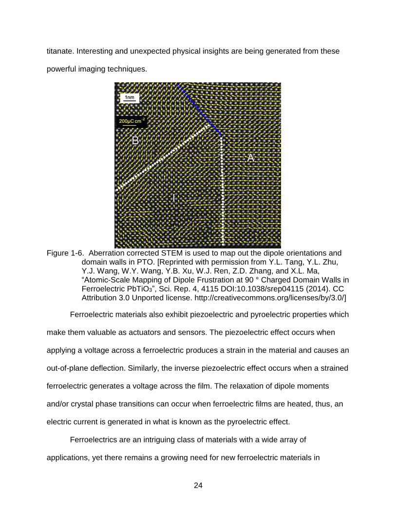
24
titanate. Interesting and unexpected physical insights are being generated from these
powerful imaging techniques.
Figure 1-6. Aberration corrected STEM is used to map out the dipole orientations and
domain walls in PTO. [Reprinted with permission from Y.L. Tang, Y.L. Zhu, Y.J. Wang, W.Y. Wang, Y.B. Xu, W.J. Ren, Z.D. Zhang, and X.L. Ma, “Atomic-Scale Mapping of Dipole Frustration at 90 ° Charged Domain Walls in Ferroelectric PbTiO3”, Sci. Rep. 4, 4115 DOI:10.1038/srep04115 (2014). CC Attribution 3.0 Unported license. http://creativecommons.org/licenses/by/3.0/]
Ferroelectric materials also exhibit piezoelectric and pyroelectric properties which
make them valuable as actuators and sensors. The piezoelectric effect occurs when
applying a voltage across a ferroelectric produces a strain in the material and causes an
out-of-plane deflection. Similarly, the inverse piezoelectric effect occurs when a strained
ferroelectric generates a voltage across the film. The relaxation of dipole moments
and/or crystal phase transitions can occur when ferroelectric films are heated, thus, an
electric current is generated in what is known as the pyroelectric effect.
Ferroelectrics are an intriguing class of materials with a wide array of
applications, yet there remains a growing need for new ferroelectric materials in

25
microelectronic applications due to a variety of limitations with conventional perovskite
ferroelectrics. As will be shown in this dissertation, the uncovered ferroelectric and
antiferroelectric properties of HfO2 thin films are particularly suited for microelectronics
and are a viable alternative to perovskite ferroelectrics.
1.2 Dissertation Organization
The organization of the dissertation begins with the general description of
ferroelectrics as described in Chapter 1. Chapter 1 covers the basic principles of
dielectrics and the resulting polarization which occurs with the application of an electric
field. The concept of ferroelectricity is then introduced and several differences are
drawn which distinguish a ferroelectric from a dielectric material. The switching
properties of conventional ferroelectrics are discussed and specific examples are taken
from the literature.
The subject of Chapter 2 is on hafnium oxide (HfO2). The properties of bulk HfO2
is first discussed to introduce the different crystal phases and the effects of doping on
the hafnia material system, many of which are applicable to thin film HfO2. This leads
into HfO2 thin film dielectrics and the efforts at enhancing the dielectric constant of HfO2
for microelectronics applications. Finally, the current state of knowledge on ferroelectric
HfO2 is overviewed along with its applications.
Chapter 3 contains a description of the various methods and techniques to
characterize ferroelectric HfO2 thin films. Chapter 3 is broadly divided into electrical and
materials characterization techniques which provide complementary data used to
understand the physics of ferroelectric thin films. While many of the electrical
measurements are specific to ferroelectric thin films, a few of the electrical tests are
more general and can be used to evaluate dielectrics and gate oxides.

26
Chapter 4 investigates the role of Si-doping in ferroelectric HfO2 thin films with
TiN and Ir capping electrodes. The Si-doped HfO2 thin films are characterized in a
metal-ferroelectric-insulator-semiconductor (MFIS) stack structure on a p+ Si substrate.
MFIS capacitors can be useful to study because they form the gate stack structure for
many ferroelectric field effect devices. A discussion of the effects of annealing, Si-
doping, the capping electrodes, and the scavenging effect on ferroelectric HfO2 are
presented in Chapter 4.
The impact of the spatial distribution of Si-dopants on the ferroelectric properties
of HfO2 is the topic of Chapter 5. Adjusting the spacing between an equal number of Si
dopant layers is shown to influence the ferroelectric properties of HfO2. Furthermore,
both the spatial distribution of Si-dopants and the overall Si doping concentration leads
to changes in the ferroelectric characteristics of HfO2. The results are particularly
relevant for FeFETs since lowering the remanent polarization can reduce the
depolarization field.
Chapter 6 presents the effects sputtered TaN electrodes had on Si-doped HfO2
thin films. A significant internal electric field was found to be present in the ferroelectric
capacitors and the cause of the imprint was investigated. Electric field cycling was
performed to investigate various aspects of the wake-up effect. Changes in the internal
electric field, relative permittivity, and remanent polarization were analyzed as a function
of cycling. X-ray photoelectron spectroscopy and high resolution transmission electron
microcopy was used to develop a model to understand the ferroelectric behavior of the
Si-doped HfO2 thin films with sputtered TaN electrodes.

27
The ferroelectric characteristics of Si-doped HfO2 thin films grown on a highly
doped p+ Ge substrate is the subject of Chapter 7. Si-doped HfO2 is incorporated into
three different devices stacks with a TaN, Ge, or SiO2/Si bottom electrode. A
comparison is drawn between the ferroelectric device performances for the different
device structures. The absence of an interfacial layer between the Si-doped HfO2
ferroelectric and Ge substrate enabled a lower operating voltage for polarization
reversal compared to the HfO2 film grown on a Si substrate. Ferroelectric HfO2 on Ge is
highlighted as an attractive prospect for future ferroelectric field effect transistors.
Chapter 8 is an investigation of the effects of co-doping HfO2 with Al and Si. By
using ALD, it was possible to manipulate the arrangement of the Al and Si dopant
monolayers within the HfO2 thin films. Three specific doping arrangements were
incorporated into the film with two sandwich doping arrangements and an alternating
dopant layering. The ferroelectric properties of the co-doped HfO2 thin films were
dependent on the dopant layering arrangement. The effects of annealing and cycling
are discussed in the context of the mixed Al and Si doped HfO2 thin films.
A study of the rapid thermal annealing dependence of Si-doped HfO2 thin films is
presented in Chapter 9. Three differently doped Si:HfO2 thin films are annealed at
various temperatures between 700 °C and 900 °C. Both isochronal and isothermal
annealing is employed to understand the effects of annealing on the properties of Si-
doped HfO2 thin films. Device characteristics such as the remanent polarization, the
leakage current, relative permittivity, cycling effects, and the breakdown field are
presented as a function of anneal time and temperature.

28
Chapter 10 is a study composed of several experiments on HfxZr1-xO2 thin films.
Al and Si incorporated into Hf0.5Zr0.5O2 which causes the undoped ferroelectric
capacitors to exhibit antiferroelectric behavior. The antiferroelectric behavior of both Al
and Si doped Hf0.5Zr0.5O2 thin films is characterized in terms of energy storage density
and efficiency. The thickness dependence and data retention of Hf0.5Zr0.5O2 thin films is
also investigated. Chapter 10 concludes with an investigation of compositionally graded
HfxZr1-xO2 thin films of different thicknesses.

29
CHAPTER 2 HAFNIUM OXIDE: BULK AND THIN FILM PROPERTIES
2.1 Background
Hafnium oxide, also referred to as hafnium dioxide or hafnia, has historically
been used in the nuclear industry due to its large neutron absorption coefficient.12 In
addition, HfO2 has a large bulk modulus, robust chemical stability, and a high melting
point which are attractive for structural applications.13 Hafnium was not discovered until
1922 due to the very similar chemical properties it shares with zirconium.14 In nature,
hafnium and zirconium are found alloyed, with zirconium being the more abundant
element. The structural and chemical properties of hafnia (HfO2) and zirconia (ZrO2) are
remarkably similar, yet important differences exist such as the crystal phase transition
temperatures.
In recent years, the microelectronics industry has brought HfO2 into its foundries
as a high-k gate dielectric to overcome the excessive tunneling leakage currents in
ultra-thin SiO2 gates due to shrinking device dimensions.15,16 State-of-the-art CMOS
devices now regularly employ nanometer-scale high-k HfO2 gate dielectrics in advanced
technology nodes. HfO2 gate dielectrics are amorphous which improves gate leakage
currents while Si doping can be used to improve thermal stability and prevent
crystallization.15 Various efforts have been undertaken to increase the dielectric
constant by doping polycrystalline HfO2 thin films so that a higher permittivity crystal
phase could be stabilized.17–19 Despite years of intense study on thin film HfO2 and no
observations of ferroelectricity, the emergence of ferroelectric behavior was finally
uncovered using a suitable combination of doping and annealing conditions in 2011.20

30
2.2 Properties of Bulk HfO2
While traditional use of bulk HfO2 has been important in nuclear applications due
to its high neutron cross-section absorption coefficient, transformation toughening in
ceramics for structural applications has been an area of great interest.12 Transformation
toughening refers to the improvement in mechanical properties of a ceramic material
during a crystal phase transition, such as the tetragonal monoclinic phase transition
in zirconia and hafnia, which can be brought about by stress or external forces. ZrO2
and ZrO2 toughened ceramics have demonstrated an exceptionally large fracture
toughness and fracture strength, but their utility in applications is limited to temperatures
less than 1000 °C due to the stabilization of the tetragonal phase above that
temperature.12 The higher tetragonal monoclinic phase transformation in HfO2 which
occurs at approximately 1700 °C could potentially be used for higher temperature
applications, although it has not demonstrated the superior mechanical properties seen
in ZrO2.12
Nonetheless, HfO2 and ZrO2 form a completely miscible solid solution system
which can be expressed as HfxZr1-xO2. Phase transition temperatures and the melting
point of HfxZr1-xO2 increases as the Hf content increases.21 Figure 2-1 illustrates the
phase diagram of the HfxZr1-xO2 solid solution system. There is a notable hysteresis in
the monoclinic and tetragonal phase transition temperatures when heating and cooling
which is more prominent in ZrO2 than HfO2.
Although under ambient pressure HfO2 undergoes a monoclinic tetragonal
cubic liquid phase transition with increasing temperature, high pressures can lead to
the formation of an orthorhombic phase.12,22,23 Figure 2-2 shows the bulk HfO2 phase
diagram as a function of pressure and temperature. There has been a wide variation in

31
the reported pressures that led to the observation of the orthorhombic phase in bulk
HfO2.12 Figure 2-3 illustrates some of the unit lattice cells of the monoclinic (P21/c) and
orthorhombic (Pbc21, Pbca, and Pnma) crystal structures that have been reported in
ZrO2 or HfO2.23
Figure 2-1. Phase diagram of the HfxZr1-xO2 solid solution system. [Reprinted with
permission from R. Ruh, H.J. Garrett, R.F. Domagala, and N.M. Tallan, J., “The System Zirconia-Hafnia”, Am. Ceram. Soc. 51, 23 (1968). Copyright 2006, John Wiley and Sons]
It has been been noted that doping HfO2 with a variety of compounds, such as
MgO, Y2O3, and Yb2O3, can influence the stabilization of the tetragonal and cubic
phases, whereby the dopant typically lowers the phase transition temperatures.12 While
studying the crystal structure of partially stabilized Mg-doped zirconia at low
temperatures and under hydrostatic pressure, Kisi was the first to conjecture the
existence of an orthorhombic Pbc21 crystal phase which originated from a
tetragonalorthorhombic phase transformation.24 The orthorhombic Pbc21 phase
(which is more appropriately written as the Pca21 space group)25 would later be called
upon to explain the origin of ferroelectricity in HfO2.20

32
Figure 2-2. Phase diagram of HfO2 with temperature and pressure. [Reprinted with
permission from J. Wang, H.P. Li, and R. Stevens, “Hafnia and Hafnia Toughened Ceramics”, J. Mater. Sci. 27, 5397 (1992). Copyright 1992, Springer]
Figure 2-3. Unit lattice cells of some crystal phases of HfO2 and ZrO2. Large atoms are
the metal cations and small atoms are the oxygen anions. [Reprinted with permission from J.E. Lowther and J.K. Dewhurst, “Relative Stability of ZrO2 and HfO2 Structural Phases”, Phys. Rev. B 60, 485 (1999). 1999 Copyright by the American Physical Society]

33
2.3 HfO2 Thin Film Properties
2.3.1 HfO2 as a High-K Gate Material
A surge of research into HfO2 thin films took place in early 2000 as various high-k
gate materials were being investigated to replace SiO2 as the gate oxide for CMOS
transistors.15,16,26,27 The replacement of SiO2 in CMOS devices became necessary due
to the excessive tunneling currents which occurred in SiO2 film with thicknesses on the
order of 1.2 nm and below.28 For continuing the scaling of device geometries, high-k
gate dielectrics were sought after since their higher permittivity could enable thicker
films which prevented tunneling currents while maintaining the equivalent oxide
thickness (EOT). The equivalent oxide thickness (teq) can be calculated by
khigh
khigh
SiOeq
tt
2
(2-1)
where εSiO2 is the silicon dioxide relative permittivity (3.9), thigh-k is the thickness of the
high-k dielectric, and εhigh-k is the relative permittivity of the high-k material.
Several high-k candidates arose as potential replacements for the traditional
SiO2 gate oxide including Al2O3, Si3N4, ZrO2, HfO2, Ta2O5, TiO2, and SrTiO3. The
polarizability of a material tends to increase as the size of its atoms increases because
the outer electrons are more loosely bound to the nuclei. For this reason, transition
metal oxides became prime candidates due to their high dielectric constants.28 While a
high permittivity material was required to replace SiO2, it was observed that higher
dielectric constants could only be obtained at the cost of smaller bandgaps (EG) and
lower breakdown fields (EBD), as shown in Figure 2-4. Band offsets and interfacial
reactions with the Si substrate were also important factors in evaluating the suitability of
high-k dielectrics as replacements for SiO2.15,28

34
High-k gate materials such as Al2O2 and Si3N4 did not improve upon the dielectric
constant of SiO2 enough to satisfactorily replace it, despite having a high breakdown
field and large bandgap. On the other end of the spectrum, SrTiO3 and TiO2 exhibited
very large dielectric constants (> 75) but have small bandgaps and poor thermal stability
on the Si substrate. Ta2O5 was also a promising high-k gate dielectric candidate
because of its high relative permittivity and moderate ~4eV bandgap, but its poor
interfacial stability with the Si substrate ultimately proved prohibitive for incorporation
into CMOS transistors.
Figure 2-4. Breakdown field and bandgap of various high-k materials plotted against
the dielectric constant. [Adapted with permission from Mater. Sci. Eng. R Reports, R 72/6, J.H. Choi, Y. Mao, and J.P. Chang, “Development of Hanfnium Based High-k Material – A Review”, 97-136, Copyright (2011), with permission from Elsevier]
The high dielectric constant of HfO2 and ZrO2 (k ~ 20-25) is balanced by a
reasonably large breakdown field and bandgap. Thus, both Zr-based and Hf-based
transition metal oxides became viable high-k dielectric candidates to replace SiO2.
However, ZrO2 is not as thermally robust as HfO2 since it exhibits a lower crystallization
temperature and a silicide (ZrSi2) may form at the Si surface.28 In contrast, HfO2 exhibits

35
excellent thermal stability on the Si substrate where the formation of a hafnium silicate
interface can improve the interface trap density.27
The interface between HfO2 and the Si channel in CMOS transistors often
benefits from the growth of a sub-nanometer layer of SiO2.29 Once the HfO2-based gate
oxide has been deposited, a variety of subsequent thermal steps may lead to an
increase in the interfacial layer thickness and a concomitant increase in the equivalent
oxide thickness. In order to mitigate interfacial layer growth in HfO2 gate dielectrics with
subsequent annealing steps, scavenging techniques were developed to improve the
HfO2/Si interface.30–32
There are two different scavenging techniques that can be used to reduce the
interfacial layer. In direct scavenging, the HfO2 thin film incorporates a dopant which will
getter oxygen during annealing. Indirect scavenging occurs when oxygen from the
interfacial layer is scavenged by the gate electrode material. TiN and TaN are common
gate scavenging electrode materials.30 Figure 2-5 illustrates the different cases for direct
and indirect scavenging. Note that in direct scavenging, the HfO2 thin film can be doped
during deposition or dopant diffusion from the metal gate into HfO2 can occur during
annealing. In both direct scavenging cases, the scavenging element is incorporated into
the HfO2 thin film.
Figure 2-5. Direct and indirect scavenging techniques.

36
Ever since it was first incorporated into commercial production when Intel
announced ALD HfO2 gate oxides at the 45 nm node in 2007, HfO2-based high-k
dielectrics have endured as the most attractive high-k metal gate material.28 The
advancements in processing technology and the competitive nature of the
semiconductor industry has driven transistors from conventional planar devices to
intricately engineered 3D geometries, as shown in Figure 2-6. Despite the myriad
changes that have occurred to transistor structures since 2007, Hf-based gate
dielectrics have remained unchallenged in advanced CMOS technology nodes.
Figure 2-6. PMOS and NMOS transistor structures for Intel’s 22 nm node. [Reprinted
with permission from R.D. Clark, “Emerging Applications for High K Materials in VLSI Technology”, Materials (Basel). 7, 2913 (2014) DOI: 10.3390/ma7042913, CC Attribution 3.0 Unported license, http://creativecommons.org/licenses/by/3.0/]
2.3.2 Enhancing the Dielectric Constant of HfO2
Due to HfO2’s use as both a dielectric material in transistors and metal-insulator-
metal (MIM) capacitors for DRAM applications, there has been interest in enhancing its
dielectric constant to improve device performance. Amorphous HfO2 has a dielectric
constant of about 20 while the monoclinic crystal phase most commonly observed at
room temperature in HfO2 has a lower dielectric constant of approximately 16.13,17
Hence, not only are amorphous HfO2 films preferred for gate transistors due to their

37
lower leakage currents, but the relative permittivity of amorphous films is also higher
than monoclinic HfO2. Nonetheless, achieving a higher dielectric constant in
polycrystalline HfO2 thin films may have advantages if a higher permittivity crystal phase
could be stabilized.
The three most commonly observed crystal phases in HfO2 are the monoclinic,
tetragonal, and the cubic phases. The dielectric constant of the tetragonal and cubic
phases of HfO2 is 70 and 29 respectively, marking a significant improvement in the
relative permittivity compared to amorphous HfO2 films.13 While monoclinic HfO2 is
typically seen at room temperature, higher temperatures can lead to phase transitions
toward the tetragonal and then to the cubic crystal phases.12 Chemically doping bulk
HfO2 or ZrO2 can lower the crystal phase transition temperatures and may lead to the
partial stabilization of the tetragonal or cubic phase.12
Doping polycrystalline HfO2 thin films with Si was found to stabilize the tetragonal
phase and increased the dielectric constant for doping concentrations less than 10
atomic %.17 Ab initio simulations have shown that Si-doping makes the monoclinic
phase less energetically stable than the tetragonal phase due to the shorter Si-O bond
length stretching in the tetragonal phase compared to the monoclinic phase in HfO2.33
Figure 2-7 illustrates the measured dielectric constant in Hf1-xSixO2 films for the
amorphous, monoclinic, and tetragonal phases. For low Si doping concentrations (< 10
atomic %), an annealing temperature of 800 °C is sufficient to crystallize the HfO2 thin
films. Higher Si doping concentrations increases the crystallization temperature of HfO2,
leading to amorphous films for both 400 °C and 800 °C anneal temperatures as shown

38
in Figure 2-7. A decrease in the dielectric constant of amorphous HfO2 occurs at very
high Si-doping concentrations because of the lower polarizability of Si compared to Hf.33
La and Y doping of HfO2 thin films were found to stabilize the cubic phase and
resulted in an increase in the relative permittivity.18,34 La doping also increases the
crystallization temperature of HfO2 but Y doping has little influence on it.19 Zr-rich Hf1-
xZrxO2 polycrystalline thin films exhibited an improved dielectric constant of about 35
due to the favorable formation of the tetragonal phase.35
Figure 2-7. The measured dielectric constant of Hf1-xSixO2 as a function of Si
concentration. The dielectric constant is greatly impacted by the structure of the film as indicated by a, m, and t which stand for amorphous, monoclinic, and tetragonal respectively. [Reprinted with permission from K. Tomida, K. Kita, and A. Toriumi, “Dielectric Constant Enhancement Due to Si Incorporation into HfO2”, Appl. Phys. Lett. 89, 142902 (2006). Copyright 2006, AIP Publishing LLC.]
In contrast to traditional doping, using a discrete ZrO2 capping layer on HfO2 was
found to induce the tetragonal phase in HfO2 thin films which was conjectured to be
because the discrete layers of ZrO2 and HfO2 crystallized separately, thus enabling the
tetragonal ZrO2 capping layer to serve as a template for the HfO2 layer by making the

39
monoclinic phase less favorable.36 TiN, a traditional capping gate electrode material,
was also found to encourage the tetragonal phase in HfO2 thin films after post-
metallization anneals by preventing the volume expansion associated with the
tetragonal to monoclinic phase transition through the mechanically constraining effect of
the electrode.37 As shown in Figure 2-8, post metallization anneals with a TiN capping
electrode reduced the surface roughness of the HfO2 thin films after annealing which
resulted in improved leakage current characteristics.
Figure 2-8. Atomic force microscopy scans of HfO2 thin films annealed at 1000 °C with
and without a TiN electrode. The temperatures listed are deposition temperatures. The surface roughness and maximum Z value of the films are shown in the figure. [Reprinted with permission from D.H. Triyoso, P.J. Tobin, B.E. White, R. Gregory, and X.D. Wang, “Impact of Film Properties of Atomic Layer Deposited HfO2 Resulting from Annealing with a TiN Capping Layer”, Appl. Phys. Lett. 89, 132903 (2006). Copyright 2006, AIP Publishing LLC.]
2.4 Ferroelectricity in HfO2-Based Thin Films
In 2011, the first observations of ferroelectric behavior in 10 nm thick Si-doped
HfO2 thin films was reported by Böscke et al.20 Böscke first encountered ferroelectric
properties in HfO2 thin films at Qimonda in 2007 while investigating enhanced dielectrics
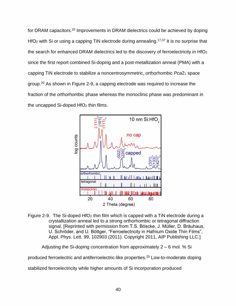
40
for DRAM capacitors.25 Improvements in DRAM dielectrics could be achieved by doping
HfO2 with Si or using a capping TiN electrode during annealing.17,37 It is no surprise that
the search for enhanced DRAM dielectrics led to the discovery of ferroelectricity in HfO2
since the first report combined Si-doping and a post-metallization anneal (PMA) with a
capping TiN electrode to stabilize a noncentrosymmetric, orthorhombic Pca21 space
group.20 As shown in Figure 2-9, a capping electrode was required to increase the
fraction of the orthorhombic phase whereas the monoclinic phase was predominant in
the uncapped Si-doped HfO2 thin films.
Figure 2-9. The Si-doped HfO2 thin film which is capped with a TiN electrode during a crystallization anneal led to a strong orthorhombic or tetragonal diffraction signal. [Reprinted with permission from T.S. Boscke, J. Muller, D. Brauhaus, U. Schroder, and U. Bottger, “Ferroelectricity in Hafnium Oxide Thin Films”, Appl. Phys. Lett. 99, 102903 (2011). Copyright 2011, AIP Publishing LLC.]
Adjusting the Si-doping concentration from approximately 2 – 6 mol. % Si
produced ferroelectric and antiferroelectric-like properties.20 Low-to-moderate doping
stabilized ferroelectricity while higher amounts of Si incorporation produced

41
antiferroelectric-like behavior.20 Figure 2-10 shows the hysteresis characteristics and
piezoelectric displacement of the HfO2 thin films doped with 3.8 mol. % Si and 5.6 mol.
% Si which exhibited ferroelectric and antiferroelectric-like properties respectively. The
ability to change the behavior of HfO2 thin films with Si doping concentration can be
useful to tailor the capacitor properties for specific applications such as memory or
energy storage.
Soon after the first report of ferroelectricity in Si-doped HfO2, binary Hf0.5Zr0.5O2
thin films from 7.5 nm to 9.5 nm thick were also shown to exhibit ferroelectricity.38 In
contrast to Si-doped HfO2 thin films which were annealed at 1000 °C and had a
crystallization temperature above 500 °C, the Hf0.5Zr0.5O2 thin films were crystallized
during the top TiN electrode deposition at 450 °C.20,38
Figure 2-10. Hysteresis and piezoelectric displacement curves illustrate how Si doping can lead to ferroelectric and antiferroelectric-like characteristics. [Reprinted with permission from T.S. Boscke, J. Muller, D. Brauhaus, U. Schroder, and U. Bottger, “Ferroelectricity in Hafnium Oxide Thin Films”, Appl. Phys. Lett. 99, 102903 (2011). Copyright 2011, AIP Publishing LLC.]

42
The low thermal budget and the excellent polarization retention at room temperature
make Hf0.5Zr0.5O2 particularly suitable for FRAM applications where back end CMOS
processing requires low anneal temperatures.38 Approximately 10 nm thick films of ZrO2
and Hf0.3Zr0.7O2 exhibited antiferroelectric properties where the critical field associated
with a field-induced phase transition decreased with a decrease in temperature.39 Figure
2-11 shows the HfxZr1-xO2 solid soluble thin film system in which ferroelectric and
antiferroelectric characteristics are determined by the relative concentration of Hf to Zr.
Figure 2-11. The hysteresis and relative permittivity indicates a paraelectric to ferroelectric phase transition as the composition of HfO2 is modified with Zr until a Hf0.5Zr0.5O2 film composition is reached. Further increasing the Zr content yields antiferroelectric behavior all the way to pure ZrO2 thin films. [Adapted with permission from J. Müller, T.S. Böscke, U. Schröder, S. Mueller, D. Bräuhaus, U. Böttger, L. Frey, and T. Mikolajick, “Ferroelectricity in Simple Binary ZrO2 and HfO2”, Nano Lett. 12, 4318 (2012). Copyright 2012 American Chemical Society.]
The behavior of polycrystalline undoped HfO2 thin films tend to form the
monoclinic phase while pure ZrO2 has a predominately tetragonal polycrystalline
structure.39 This can be understood to arise from the smaller critical grain size of the
tetragonal phase in HfO2 (~7 nm – 10 nm) compared to ZrO2 (~ 30 nm) – since grain
sizes smaller than 30 nm are readily achieved in polycrystalline ZrO2, the tetragonal

43
phase is favored.40 Simulations have shown that ZrO2 can exhibit antiferroelectricity
through a reversible field-induced tetragonal orthorhombic phase transition.41 Further
theoretical simulations carried out by Materlik et al. found that the ferroelectric
orthorhombic phase was unstable in bulk Hf0.5Zr0.5O2 but could be stabilized by
introducing a phenomenological surface energy term into the Helmholtz free energy,
thus accounting for ferroelectricity being observed in nanoscale Hf0.5Zr0.5O2 thin films to
5 nm.42
Due to the critical grain size of the tetragonal phase and surface energy effects in
thin film Hf0.5Zr0.5O2, the formation of the polar orthorhombic ferroelectric phase can be
influenced by the film thickness. Park et al. studied the effect of the anneal temperature
and film thickness on the ferroelectric characteristics and polycrystalline structure of
Hf0.5Zr0.5O2 thin films.40 As shown in figure 2-12, Hf0.5Zr0.5O2 films thicker than 10 nm
showed an increase in the fraction of the monoclinic phase and were accompanied by a
lower remanent polarization and relative permittivity. The degradation of the ferroelectric
properties with increasing film thickness can be prevented by inserting a dielectric
insulator layer within Hf0.5Zr0.5O2 to engineer smaller grain sizes and make the formation
of the ferroelectric orthorhombic phase more favorable.43
HfO2 thin films doped with Yttrium in the range of 2 – 5 mol. % exhibited
ferroelectricity after either a post-deposition or a post-metallization anneal.44
Ferroelectricity was enhanced when Y-doped HfO2 was annealed with a capping
electrode as has been observed for Al-doped HfO2 as well as Hf0.5Zr0.5O2.44–46
Ferroelectric Y-doped HfO2 thin films have been fabricated with a variety of deposition
techniques including ALD, sputtering, and chemical solution deposition.44,47,48 The

44
remanent polarization of Y-doped HfO2 was largest in films that were deposited by
atomic layer deposition, indicating that ALD produces the highest quality ferroelectric
HfO2-based thin films.44
Figure 2-12. The 2Pr and relative phase fraction of Hf0.5Zr0.5O2 films from 5.5 nm to 25
nm thick as a function of anneal temperature. [Reprinted with permission from M. Hyuk Park, H. Joon Kim, Y. Jin Kim, W. Lee, T. Moon, and C. Seong Hwang, “Evolution of Phases and Ferroelectric Properties of Thin Hf0.5Zr0.5O2 Films According to the Thickness and Annealing Temperature”, Appl. Phys. Lett. 102, 242905 (2013). Copyright 2011, AIP Publishing LLC.]
Other dopants which have been incorporated in HfO2 thin films to encourage the
formation of the ferroelectric orthorhombic phase include Sr, Gd, and La.49 A wide
compositional doping range from approximately 3 – 22 mol. % of Sr was found to

45
stabilize ferroelectricity in Sr-doped HfO2 and is the largest doping range reported to
date for the trace dopants.50 At the time of writing, the highest Pr found in HfO2-based
ferroelectrics is 40 µC/cm2 in La-doped HfO2, although more reports are needed to
confirm the reproducibility of this result.25,49 The first direct confirmation of the presence
of the polar Pca21 orthorhombic phase was measured by aberration corrected high-
angle annular dark-field (HAADF) scanning electron microscopy (STEM) in Gd-doped
HfO2 and unambiguously proved the origins of ferroelectricity predicted by simulations.51
Figure 2-13 illustrates the crystal structures and space groups of the monoclinic,
tetragonal, and orthorhombic phases projected along the major axes. The coordination
of the Hf-atoms in all of the orthorhombic space groups are the same, but the
arrangement of the oxygen atoms are different.51 Figure 2-14 confirms the presence of
the orthorhombic phase in the Gd-doped HfO2 thin films. Since all of the Hf atomic
positions are the same in all three orthorhombic space groups, position averaged
convergent beam electron diffraction (PACBED) was used to determine the symmetry
and polarity of the orthorhombic phase and distinguished between the space groups.51
PACBED confirmed the presence of the polar, noncentrosymmetric Pca21 orthorhombic
space group responsible for the ferroelectric behavior in HfO2-based thin films.51

46
Figure 2-13. Different crystal phases of hafnium oxide. A) The crystal structures of HfO2
for the tetragonal (P21/c), monoclinic (Pmn21), and orthorhombic (Pca21, Pbcm, and Pbca) crystal phases projected along the major axes. B) Measured GIXRD pattern of Gd-doped HfO2 and reference GIXRD patterns from powder-diffraction phases of HfO2. [Reprinted with permission from X. Sang, E.D. Grimley, T. Schenk, U. Schroeder, and J.M. LeBeau, “On the Structural Origins of Ferroelectricity in HfO2 Thin Films”, Appl. Phys. Lett. 106, 162905 (2015). Copyright 2015, AIP Publishing LLC.]

47
Figure 2-14. STEM is used to identify the polar orthorhombic phase. A) STEM of Gd-doped HfO2. B) The HAADF-STEM images provide direct confirmation of the orthorhombic crystal structure in Gd-doped HfO2. [Reprinted with permission from X. Sang, E.D. Grimley, T. Schenk, U. Schroeder, and J.M. LeBeau, “On the Structural Origins of Ferroelectricity in HfO2 Thin Films”, Appl. Phys. Lett. 106, 162905 (2015). Copyright 2015, AIP Publishing LLC.]
2.5 Applications for Ferroelectric and Antiferroelectric HfO2
Ferroelectric HfO2-based thin films have great potential for microelectronics
nonvolatile memory technologies. In one type of nonvolatile memory technology called
ferroelectric random access memory (FRAM), HfO2 can serve as the ferroelectric in the
conventional metal-ferroelectric-metal (MFM) capacitor geometry. In FRAM, the
polarization state of the ferroelectric capacitor is directly interrogated by pulsing the
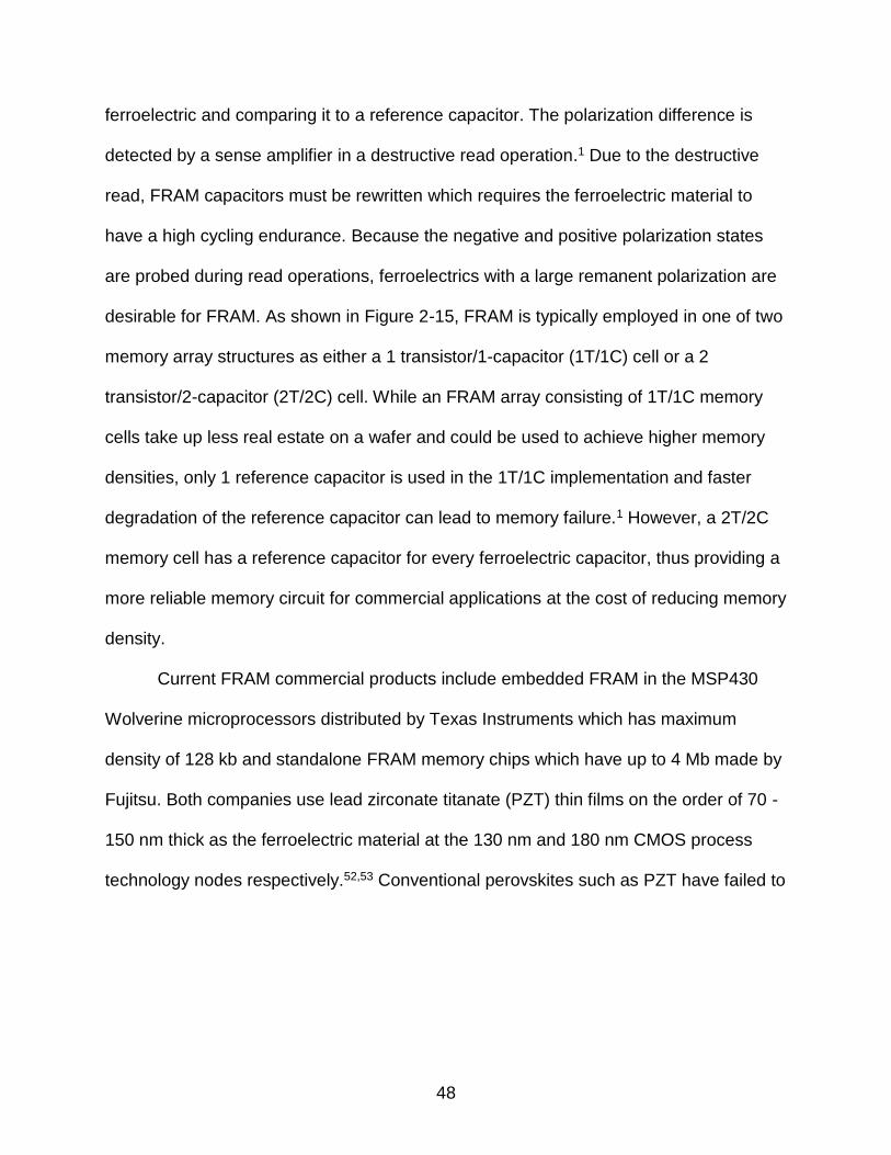
48
ferroelectric and comparing it to a reference capacitor. The polarization difference is
detected by a sense amplifier in a destructive read operation.1 Due to the destructive
read, FRAM capacitors must be rewritten which requires the ferroelectric material to
have a high cycling endurance. Because the negative and positive polarization states
are probed during read operations, ferroelectrics with a large remanent polarization are
desirable for FRAM. As shown in Figure 2-15, FRAM is typically employed in one of two
memory array structures as either a 1 transistor/1-capacitor (1T/1C) cell or a 2
transistor/2-capacitor (2T/2C) cell. While an FRAM array consisting of 1T/1C memory
cells take up less real estate on a wafer and could be used to achieve higher memory
densities, only 1 reference capacitor is used in the 1T/1C implementation and faster
degradation of the reference capacitor can lead to memory failure.1 However, a 2T/2C
memory cell has a reference capacitor for every ferroelectric capacitor, thus providing a
more reliable memory circuit for commercial applications at the cost of reducing memory
density.
Current FRAM commercial products include embedded FRAM in the MSP430
Wolverine microprocessors distributed by Texas Instruments which has maximum
density of 128 kb and standalone FRAM memory chips which have up to 4 Mb made by
Fujitsu. Both companies use lead zirconate titanate (PZT) thin films on the order of 70 -
150 nm thick as the ferroelectric material at the 130 nm and 180 nm CMOS process
technology nodes respectively.52,53 Conventional perovskites such as PZT have failed to

49
Figure 2-15. Two different forms of the FRAM memory cell. A) 1T/1C and B) 2T/2C memory architectures for FRAM applications. [Reprinted figure with permission from M. Dawber, K.M. Rabe, and J.F. Scott, “Physics of Thin Film Ferroelectric Oxides”, Rev. Mod. Phys. 77, 1083 (2005). Copyright 2005 by the American Physical Society.]
garner widespread industry adoption of FRAM due to the potential for Pb contamination
in CMOS foundries, poor scaling properties, limited memory array densities, and
reliability concerns such as imprint and data retention. Table 2-1 shows a comparison of
FRAM with commonly used nonvolatile memory technologies, electrically erasable
programmable read only memory (EEPROM) and FLASH. While technology
improvements since the year 2000 would require some modifications to the
performance specifications in Table 2-1, the overall comparison trends highlight the
relevant differences in the nonvolatile memory technologies.
Table 2-1. Conventional nonvolatile memory technologies compared with FRAM. Nonvolatile
Memory Area/Cell
(Normalized) Read Access
Time Write Access
Time Energy per
32b Write Energy per
32b Read
EEPROM 2 50ns 10µs 1µj 150pJ FLASH 1 50ns 100ns 2µj 150pJ FRAM 5 100ns 100ns 1nj 1nJ
© 2000 IEEE [Reprinted, with permission, from A. Sheikholeslami and P.G. Gulak, “A Survey of Circuit Innovations in Ferroelectric Random-Access Memories”, Proc. IEEE 88, 667 (2000).]
The cell size of FLASH is much smaller than current FRAM technologies which
enables far higher memory array densities than FRAM due to scaling limitations of

50
conventional ferroelectric perovskites. Ferroelectric HfO2-based thin films are well-suited
to surpass the material issues associated with limited FRAM scaling because HfO2-
based thin films possess ferroelectricity down to 5 nm in thickness.54 3-dimensional
trench capacitors using ferroelectric Al-doped HfO2 have demonstrated the intriguing
scaling potential of HfO2-based ferroelectrics for FRAM applications,55 as illustrated in
Figure 2-16. The conformal ALD growth of HfO2 and the feasibility of obtaining
ferroelectricity in ultra-thin HfO2 films make integration of 3D structures a practical
solution to obtain higher density FRAM arrays. While the polar orthorhombic crystal
phase in HfO2-based thin films benefits from film thicknesses on the order of 10 nm,40
PZT capacitors degrade when scaled to the same thicknesses with a large increase in
the coercive field and a decline in the remanent polarization.56,57 PZT is also known to
be very sensitive to hydrogen and requires a barrier layer to prevent its ferroelectric
properties from degrading58 whereas HfO2-based thin films are resilient against
hydrogen contamination.59 Forming gas anneals containing hydrogen are routinely
employed to achieve optimal transistor performance on Si wafers.59
Another advantage FRAM has over conventional FLASH and EEPROM
technologies is the much lower energy needed to perform a write operation. The energy
required to write to FRAM is 1000x smaller than either FLASH or EEPROM, making it
very attractive for low-power, mobile devices. Though HfO2-based ferroelectrics may be
in a position to pivot FRAM technologies toward higher densities and expand FRAM’s
presence in mobile devices, it must compete with other emerging nonvolatile memories
such as resistive random access memory (RRAM), magnetic random access memory

51
(MRAM), phase change memory (PCM), and spin transfer torque random access
memory (STT-RAM).
Figure 2-16. Process flow and cross-sectional image of 3D trench capacitors
incorporating Al-doped HfO2 are shown along with the equivalent planar area hysteresis measurement. © 2000 IEEE [Reprinted with permission from P. Polakowski, S. Riedel, W. Weinreich, M. Rudolf, J. Sundqvist, K. Seidel, and J. Muller, “Ferroelectric deep trench capacitors based on Al:HfO2 for 3D

52
nonvolatile memory applications”, in 2014 IEEE 6th Int. Mem. Work. (IEEE, 2014), pp. 1–4.]
Table 2-2. Comparison of emerging alternative nonvolatile memory technologies.
Features FRAM MRAM STT-RAM PCM
Cell size (F2) Large, ~40 – 20 Large, ~25 Small, ~6 – 20 Small, ~8 Storage
Mechanism Polarization of a ferroelectric
Magnetization of a ferromagnet in a MTJ
Spin polarized current applies torque on magnetic moment
Amorphous/polycrystalline phase change
Read Time (ns)
20 – 80 3 – 20 2 – 20 20 – 50
Write/Erase Time (ns)
50/50 3 – 20 2 – 20 20/30
Endurance >1012 >1015 >1016 >1012 Write Power Mid Mid to high Low Low Nonvolatility Yes Yes Yes Yes Maturity Limited production Test chips Test chips Test chips Applications Low density Low density High density High density
© 2014 Nanoscale Research Letters [Adapted with permission from J. Meena, S. Sze, U. Chand, and T.-Y. Tseng, Nanoscale Res. Lett. 9, 526 (2014). CC Attribution 4.0 license, http://creativecommons.org/licenses/by/4.0/]
RRAM is considered to be one of the most promising alternative candidates due to its
small cell structure compared to MRAM and STT-RAM while also operating faster than
PCM. Table 2-2 gives a comparison of FRAM, MRAM, STT-RAM, and PCM. The
performance specifications for FRAM assume PZT or SBT is the ferroelectric material,
but table 2-2 does not take into account what cell size may be achievable with
ferroelectric HfO2-based thin films.60
While FRAM is a memory technology under development, there remains other
ferroelectric-based nonvolatile memories which are emerging and still in the research
phase. One emerging nonvolatile memory device is the ferroelectric field effect
transistor (FeFET) which has a simple 1 transistor (1T) memory cell. FeFETs
incorporate a ferroelectric material as the gate. By switching the polarization state of the
ferroelectric, the threshold voltage can be shifted. A memory window is established by

53
the difference in the threshold voltages for the two polarization states in a FeFET.61 One
major hindrance to the successful demonstration of FeFETs has been the poor data
retention when perovskite materials are used as the gate material.1 The poor data
retention in FeFETs is primarily due to a depolarization field generated from the lack of
compensating charge carriers at the ferroelectric-semiconductor interface in the MFS
stack.62 Perovskite ferroelectrics tend to exhibit poor interfacial stability on Si, but when
an insulating buffer layer is sandwiched between the ferroelectric and the Si channel,
the resulting MFIS device structure exacerbates the depolarization field.62 The
depolarization field in a FeFET can be expressed as62
1F
ISr
rDep
C
C
PE
(2-1)
where Pr is the remanent polarization, εr is the relative permittivity of the ferroelectric,
CIS is the interfacial layer capacitance, and CF is the ferroelectric capacitance. Eq. 2-1
shows that if the thickness of the interfacial layer could be reduced to zero (i.e. CIS goes
to infinity), then the depolarization field could effectively be neutralized. Due to the
addition of a buffer layer or the growth of interfacial layers, thick perovskite ferroelectric
films must be employed to mitigate depolarization fields in ferroelectric field effect
transistors which make perovskites unsuitable for advanced CMOS technology nodes.25
Ferroelectric HfO2-based thin films are excellent candidates for FeFET
technologies because HfO2 is already being used as a gate dielectric materials in
advanced CMOS technologies.28 Ferroelectric Si-doped HfO2 thin films incorporated
into FeFETs have demonstrated an extrapolated 10 year memory window of 650 mV
which surpasses the best performing FeFETs based on strontium barium titanate and

54
PZT.61 Furthermore, FeFETs fabricated at the 28 nm technology node have shown the
scaling potential for ferroelectric Si-doped HfO2 thin films.63 Several challenges must be
overcome to make HfO2-based FeFETs a viable memory technology such as cycling
degradation and poor data retention at elevated temperatures, both of which are
associated with charge trapping and the interfacial SiON layer typically employed in the
MFIS stack.63,64 As will be discussed in Chapter 7, an interfacial layer between the
semiconductor and ferroelectric HfO2 may be avoided by using a different substrate
material as the basis for a ferroelectric field effect transistor and ultimately improve the
device characteristics.
In addition to FeFETs being used as a nonvolatile memory storage element, a
capacitor-less DRAM cell can be constructed in a volatile memory scheme.65 The
advantages of using a FeFET in place of a conventional DRAM capacitor include a
much smaller cell size, a longer refresh rate due to the better data retention in FeFETs,
and lower power consumption.65 Hf0.5Zr0.5O2 thin films integrated into FeFET device
structures have shown that the capacitor-less DRAM cell can exhibit superior leakage
current properties, a smaller cell size, and the potential for sub-ns switching operation
which would not be feasible in conventional 1T/1C DRAM capacitors.66 In addition to
using ferroelectric HfO2-based thin films for their memory capability in transistors,
transistor performance can be enhanced through a reduction of the subthreshold
slope.67 Antiferroelectric HfO2-based thin films may result in sub-threshold slopes down
to 33 mV/decade due to the negative capacitance effect.68
Antiferroelectric HfO2-based thin films are believed to exhibit a reversible field
induced phase transition between the polar orthorhombic phase and the tetragonal
55
phase.41 The reversible phase transition can be utilized in energy storage capacitors
because much of the electrical energy involved in the field-induced phase transition is
returned when the phase transition is reversed as the applied electric field is removed.
Park et al. quantified the energy storage density in HfxZr1-xO2 thin films which yielded an
impressive 28 J/cm3 with a 50% efficiency over a 25 °C – 175 °C temperature range.69
Furthermore, the electrocaloric effect was exhibited in antiferroelectric HfxZr1-xO2 which
could be useful for refrigeration applications.70 Practical applications for infrared
detectors based on the pyroelectric effect has been shown to be possible for
antiferroelectric Si-doped HfO2 thin films.71

56
CHAPTER 3 MEASUREMENT METHODS AND TECHNIQUES
3.1 Background
There are various electrical and materials characterization techniques that can
be used to probe the properties of ferroelectric thin films. Electrical measurements
specific to ferroelectric capacitors include hysteresis, dynamic hysteresis current
measurements, Positive-Up-Negative-Down (PUND), pulsed transient current
measurements, capacitance-voltage (CV) sweeps, endurance cycling, and retention
tests. Another electrical technique which can be used to determine specific film
properties and gain additional insight about the quality of the films is impedance
spectroscopy. While a single electrical measurement cannot provide the necessary
information to understand all of the physics in ferroelectric films, taken together, they
offer a powerful tool to evaluate a ferroelectric’s potential for many applications and
provide a canvas from which important physical insights may be drawn.
Materials characterization techniques aid in providing a more in-depth look at
both the structure and composition of ferroelectric thin film devices. While there is an
immense array of materials techniques to choose from in studying ferroelectric films,
some of the more important techniques include x-ray photoelectron spectroscopy
(XPS), time-of-flight secondary ion mass spectrometry (TOF-SIMS), grazing incidence
x-ray diffraction (GI-XRD), and transmission electron microscopy (TEM). The use of
both electrical and materials characterization techniques is complementary since
practical use of ferroelectric thin films draws almost entirely on the electrical tests while
materials techniques can unveil physical details that may not be possible through
electrical measurements.

57
3.2 Electrical Measurements and Techniques
3.2.1 Hysteresis Loops
The most frequently used technique to evaluate the ferroelectric behavior of a
material is by looking at its hysteresis characteristics. A hysteresis graph is generated
by plotting the ferroelectric’s polarization as a function of voltage or electric field
(commonly denoted as a P-V or P-E plot respectively). The Sawyer-Tower circuit is
commonly used to take hysteresis measurements.72 Figure 3-1 shows an
implementation of the Sawyer-Tower circuit which is used in extracting the P-V or P-E
curves of ferroelectric thin films. In the Sawyer-Tower circuit, a triangle wave is applied
across a ferroelectric capacitor (CF) and a series linear sense capacitor (Cs) where the
linear capacitor is grounded. The sense voltage (Vs) is measured at the terminal
between the ferroelectric capacitor and linear capacitor.
Figure 3-1. An implementation of the Sawyer-Tower used to extract the hysteresis plots
of ferroelectric capacitors.
The ferroelectric charge (QF) generated from applying a voltage across the
capacitors can be calculated by73
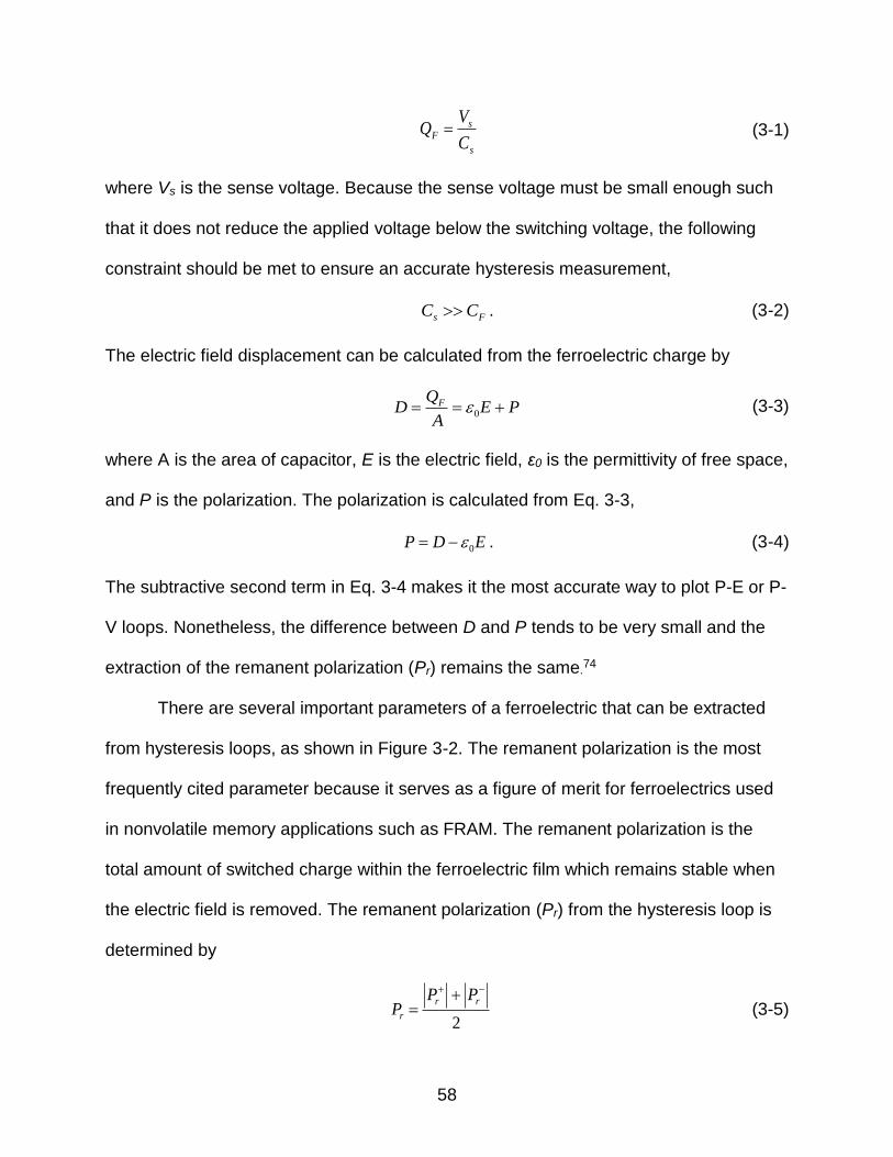
58
s
sF
C
VQ (3-1)
where Vs is the sense voltage. Because the sense voltage must be small enough such
that it does not reduce the applied voltage below the switching voltage, the following
constraint should be met to ensure an accurate hysteresis measurement,
Fs CC . (3-2)
The electric field displacement can be calculated from the ferroelectric charge by
PEA
QD F 0 (3-3)
where A is the area of capacitor, E is the electric field, ε0 is the permittivity of free space,
and P is the polarization. The polarization is calculated from Eq. 3-3,
EDP 0 . (3-4)
The subtractive second term in Eq. 3-4 makes it the most accurate way to plot P-E or P-
V loops. Nonetheless, the difference between D and P tends to be very small and the
extraction of the remanent polarization (Pr) remains the same.74
There are several important parameters of a ferroelectric that can be extracted
from hysteresis loops, as shown in Figure 3-2. The remanent polarization is the most
frequently cited parameter because it serves as a figure of merit for ferroelectrics used
in nonvolatile memory applications such as FRAM. The remanent polarization is the
total amount of switched charge within the ferroelectric film which remains stable when
the electric field is removed. The remanent polarization (Pr) from the hysteresis loop is
determined by
2
rr
r
PPP (3-5)
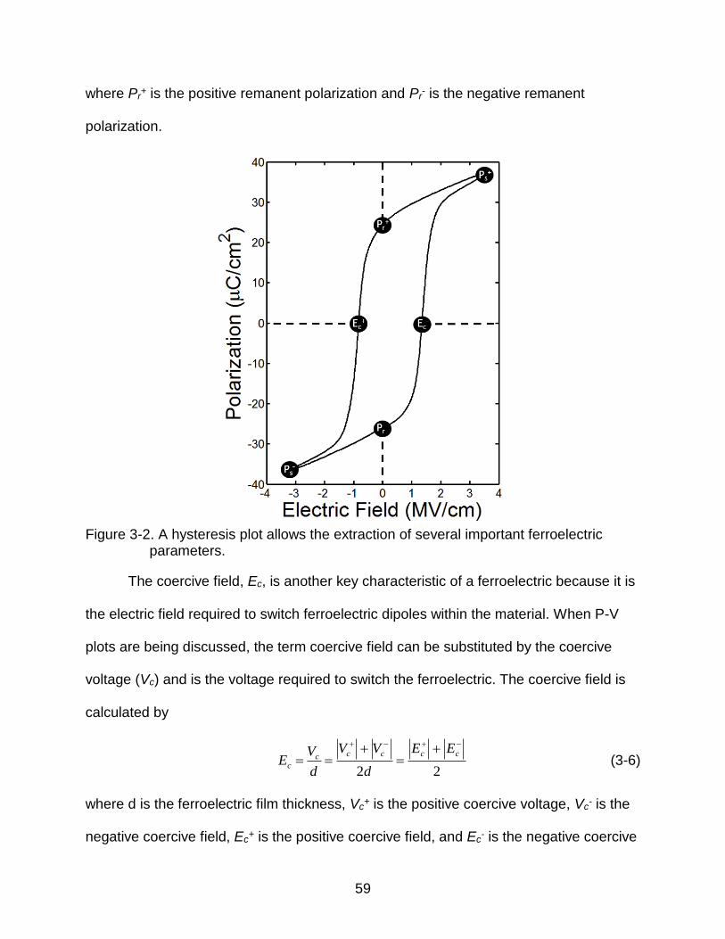
59
where Pr+ is the positive remanent polarization and Pr
- is the negative remanent
polarization.
Figure 3-2. A hysteresis plot allows the extraction of several important ferroelectric
parameters.
The coercive field, Ec, is another key characteristic of a ferroelectric because it is
the electric field required to switch ferroelectric dipoles within the material. When P-V
plots are being discussed, the term coercive field can be substituted by the coercive
voltage (Vc) and is the voltage required to switch the ferroelectric. The coercive field is
calculated by
22
cccccc
EE
d
VV
d
VE (3-6)
where d is the ferroelectric film thickness, Vc+ is the positive coercive voltage, Vc
- is the
negative coercive field, Ec+ is the positive coercive field, and Ec
- is the negative coercive

60
field. The spontaneous polarization (Ps) is the total amount of switched charge at the
maximum applied electric field and due to relaxation effects in polycrystalline
ferroelectric thin films, is always larger than the remanent polarization.
Hysteresis plots can also be used to evaluate an antiferroelectric film’s energy
storage properties. Figure 3-3 illustrates the integrated (colored) regions which can be
used to determine the energy storage density (ESD) and loss. The energy storage
density for both positive and negative fields can be determined by the following equation
22
0
2
0
1
MINMAX E
s
E
s IdEPIdEPESDESD
ESD
2
)()(0
0
0
0
MIN
MIN
MAX
MAX
E
E
s
E
E
s dEEPdEPdEEPdEP
(3-7)
where ESD+ is the positive energy storage density, ESD- is the negative energy storage
density, λ+ is the loss in the positive portion of the loop, λ- is the loss in the negative
portion of the loop, EMAX is the maximum applied electric field, EMIN is the minimum
applied electric field, I1 and I2 are integration regions, and P(E) is the polarization as a
function of the electric field. The loss (λ) can be determined by
2
)()()()(
2
0000
MINMINMAXMAX E
Bottom
E
Bottom
E
Bottom
E
Top dEEPdEEPdEEPdEEP
(3-8)
Where P+Top and P-
Top is the top of the polarization curve on the positive and negative E-
axis respectively and P+Bottom and P-
Bottom is the bottom of the polarization curve on the

61
positive and negative E-axis respectively. The energy storage efficiency (Eff) of an
antiferroelectric capacitor can be determined from Eq. 3-7 and Eq. 3-8,
ESD
ESDEff (3-9)
Figure 3-3. The energy storage density and loss of an antiferroelectric capacitor can be
determined by integrating regions within the hysteresis plot.
3.2.2 Dynamic Hysteresis Currents
A variation of the Sawyer-Tower circuit can be made by replacing the sense
capacitor with a series resistor which enables the dynamic hysteresis current
measurement (Figure 3-4). The dynamic hysteresis current density (JF) can be
determined from the sense voltage across the resistor and calculated from
AR
V
A
IJ
s
sFF (3-10)

62
where IF is the measured hysteresis current and Rs is the sense resistor.
Distorted hysteresis loops which deviate from typical ferroelectric or
antiferroelectric shapes can sometimes be observed, and in other cases, conventional
P-V plots may obscure distortions in the shape of the hysteresis loop near the coercive
voltage. Dynamic hysteresis currents give direct access to the switching currents that
ferroelectric films produce when excited by a triangle wave.
Figure 3-4. Modified Sawyer-Tower circuit for dynamic hysteresis current
measurements.
While dynamic hysteresis currents generally produce a more qualitative
understanding of the behavior of a ferroelectric than P-V plots since fewer quantitative
parameters are extracted, it can corroborate aspects of conventional hysteresis loops
and provide additional insights into the switching characteristics of a ferroelectric film.
Moreover, the critical forward phase field (EF) and the critical backward phase field (EA)
of an antiferroelectric film are easier to extract in a dynamic hysteresis current plot from
the switching current peaks as shown in Figure 3-5 (right column). The critical forward

63
phase field is associated with an antiferroelectric to ferroelectric phase transition
(AFEFE) as an electric field is applied, while the critical backward phase field is
associated with a ferroelectric to antiferroelectric (FEAFE) when the electric field is
removed.75 Electric field cycling can also lead to changes in the P-V characteristics of a
ferroelectric, and dynamic hysteresis current measurements can provide a more
detailed view of the switching current properties as illustrated in Figure 3-5 (left column).
The coercive field can also be extracted from the dynamic hysteresis current plot from
the switching current peaks. A review on the insights dynamic hysteresis current
measurements can provide was written by Schenk et al.74
Figure 3-5. Dynamic hysteresis current measurements. A) Dynamic hysteresis loops
can shed more light about the switching currents before (red) and after cycling (black). B) Four distinct switching peaks in four quadrants are a signature of an antiferroelectric film.
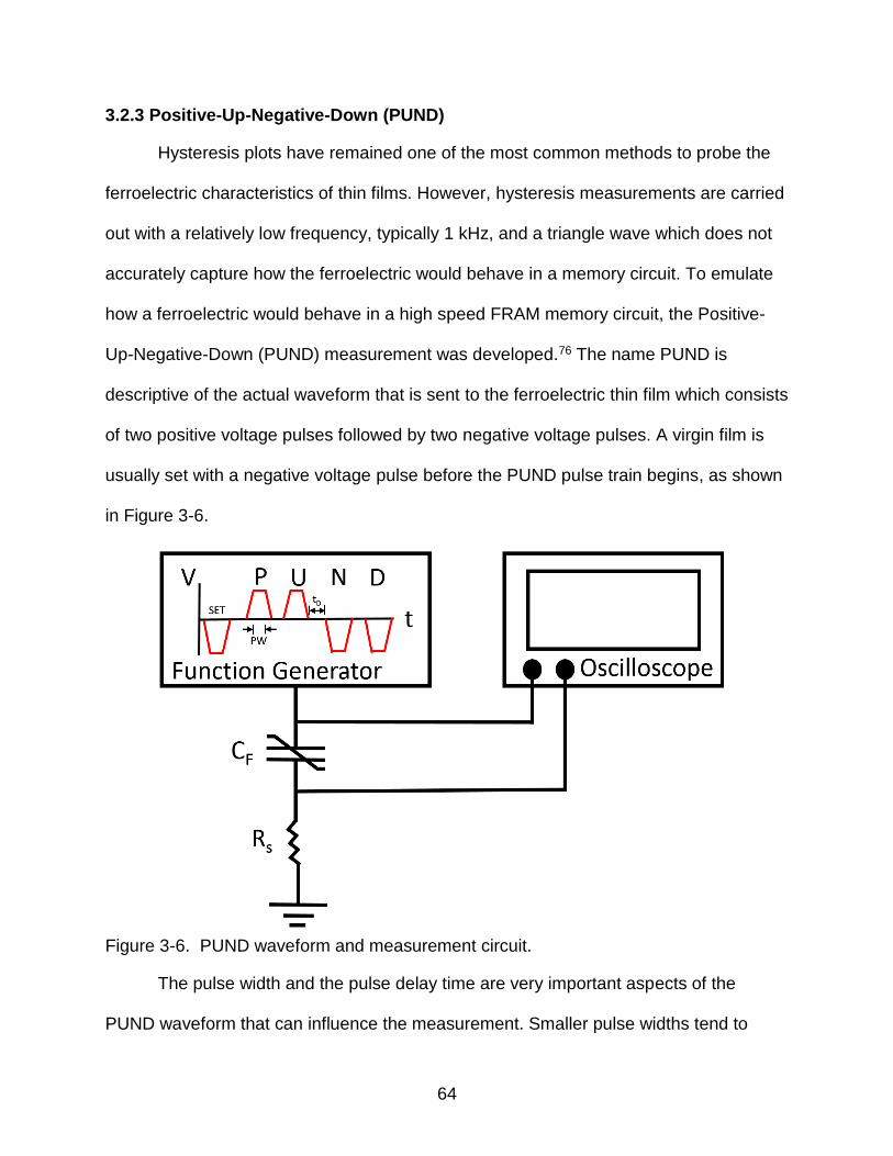
64
3.2.3 Positive-Up-Negative-Down (PUND)
Hysteresis plots have remained one of the most common methods to probe the
ferroelectric characteristics of thin films. However, hysteresis measurements are carried
out with a relatively low frequency, typically 1 kHz, and a triangle wave which does not
accurately capture how the ferroelectric would behave in a memory circuit. To emulate
how a ferroelectric would behave in a high speed FRAM memory circuit, the Positive-
Up-Negative-Down (PUND) measurement was developed.76 The name PUND is
descriptive of the actual waveform that is sent to the ferroelectric thin film which consists
of two positive voltage pulses followed by two negative voltage pulses. A virgin film is
usually set with a negative voltage pulse before the PUND pulse train begins, as shown
in Figure 3-6.
Figure 3-6. PUND waveform and measurement circuit.
The pulse width and the pulse delay time are very important aspects of the
PUND waveform that can influence the measurement. Smaller pulse widths tend to

65
decrease the amount of switched charge in the ferroelectric and may accurately
reproduce the switching properties in a higher frequency memory circuit. Since FRAM is
a nonvolatile memory and data retention is expected to last for up to 10 years,
relaxation effects in a ferroelectric must be accurately taken into account. For this
reason, 1 s pulse delays should be used when taking PUND measurements because
almost all of the polarization relaxation occurs within 1 s.76 If shorter pulse delays are
used, then the switched polarization charge will be overestimated compared to long
data retention times because of the larger contribution of the transient polarization.
Each of the terms in the PUND waveform have important physical significance.
The P term contains the total amount of positive switched charge, permanent and
transient, and the dielectric response of the ferroelectric material. The U term contains
the positive transient polarization and the dielectric response. The P and U terms are
measured by integrating the current density in Eq. 3-10
dtJP P (3-11)
dtJU U (3-12)
where JP is the measured current density from the P pulse and JU is the measured
current density from the U pulse. The N term contains the total amount of negative
switched charge, permanent and transient, and the dielectric response of the
ferroelectric material. The D term contains the negative transient polarization and the
dielectric response. The N and D terms can be calculated by
dtJN N (3-13)
dtJD D (3-14)

66
where JN is the measured current density from the N pulse and JD is the measured
current density from the D pulse. The total amount of switched ferroelectric polarization
charge that can be used in memory circuit can be calculated as
UPPSW (3-15)
DNPSW (3-16)
2
SWSW
SW
PPP (3-17)
where PSW+ is the positive switched polarization and PSW
- is the negative switched
polarization. Figure 3-7 shows an example of the PUND waveform applied to a
ferroelectric Si-doped HfO2 thin films.
Figure 3-7. The PUND waveform is applied to a ferroelectric thin film. The switching
current is extracted from the load voltage for each of the pulses and integrated to measure the amount of switched charge.

67
3.2.4 Capacitance-Voltage (CV)
Ferroelectric materials exhibit nonlinear capacitance-voltage characteristics due
to dipole or domain switching. When the thickness of the ferroelectric material is known,
it is common to extract the relative permittivity (Eq. 1-9) to generate εr as a function of
voltage. The relative permittivity can give indirect evidence about the electrical quality of
the ferroelectric while yielding potential insights about the crystal structure or growth of
interfacial layers within the films.77 Thus, the extraction of εr can aid in better
understanding the physical properties of the ferroelectric whereas the capacitance may
be more pertinent for specific electrical applications.
The CV characteristics of a ferroelectric are measured by applying a sweeping
DC voltage with a small AC signal superimposed. The AC signal must be small enough
to ensure linearity for an accurate impedance measurement while also providing a
strong enough signal. AC signals between 15 mV – 75 mV are sufficient to ensure
linearity and signal strength in solid state ferroelectric capacitors. The AC signal
frequency can be chosen based upon the application of interest, but generally 1 kHz to
100 kHz is acceptable unless the radio frequency (RF) behavior is being investigated.
The DC voltage may be swept in either a clockwise or anticlockwise direction and
always terminates at the voltage polarity from whence it commenced.
The distinctive butterfly loop of a ferroelectric material is demonstrated in Figure
3-8. The two switching peaks in the relative permittivity are associated with the
switching of domains within the ferroelectric film. The peaks occur near the coercive
voltage of a ferroelectric and can provide corroborating evidence of the switching
behavior within the thin film. The relative permittivity maxima occurs near the coercive
field because when the sweeping DC voltage approaches near the coercive field, only a

68
small AC voltage is required to switch ferroelectric domains.78 The double butterfly loop
of an antiferroelectric is also shown in Figure 3-8. Like the dynamic hysteresis current
measurements, CV sweeps can permit an easy extraction of the critical forward and
backward phase fields.
A B
Figure 3-8. C-V characteristics of ferroelectric thin films. A) The classic butterfly curve is characteristic of ferroelectric materials. B) The double butterfly loop is a signature of an antiferroelectric.
The electrodes can play a significant role in the CV behavior of a ferroelectric thin
film due to the generation of space charge regions within the ferroelectric at the
electrode interfaces.78,79 An asymmetry in the space charge regions at the two opposing
electrode interfaces can create a depolarization field.78 The switching characteristics
present in a CV plot may be modeled by the method developed by Brennan.78
Brennan’s model is largely empirical and enables the extraction of the metal Schottky
barrier heights and ionized charge concentrations at the interface, this information can
be useful in estimating defect concentrations in ferroelectric thin films.77

69
3.2.5 Endurance Cycling
Nonvolatile memory elements are typically expected to store data up to 10 years
in commercial products under certain operating conditions. However, most nonvolatile
memory devices lose their ability to store data when they have been cycled beyond a
certain point. As an example, NAND FLASH memory has a cycling endurance between
10,000 – 100,000 cycles before it loses its ability to store data.80 Cycling refers to the
exposure of a memory device to a number of write cycles. Device characteristics may
be interrogated after cycling to evaluate the device’s reliability as a memory element.
Endurance cycling measures how a memory element performs with increasing
number of write cycles until device failure occurs. PZT-based FRAM capacitors have an
impressive cycling endurance of > 1012 cycles.52 A high cycling endurance is a
requirement for FRAM applications because of the destructive read operation.
Moreover, excellent cycling endurance is valuable for all types of nonvolatile memories
and is an extremely important reliability metric. Cycling endurance tests are needed to
evaluate the potential of new materials for nonvolatile memories and may highlight
where improvements need to be made for viable technologies.
Ferroelectric capacitors can be cycled with a series resistor as shown in the
circuit in Figure 3-9. Bipolar cycles should always be used when evaluating a
ferroelectric for nonvolatile memory applications because it most closely resembles
memory circuit operation. A basic procedure for evaluating the cycling characteristics of
a ferroelectric capacitor consists of exposing the capacitor to a set number of bipolar
square waves and then implementing measurements of interest such as hysteresis,
PUND, or CV for example. It should be noted that when low-frequency measurements
are being alternated with endurance cycling, such as the slow sweeping DC voltage of a

70
CV scan or a leakage current measurement, the ferroelectric’s behavior may be
influenced by the relatively long exposure time to an appreciable voltage. In this case, a
new capacitor should be used for every cycling measurement.
Figure 3-9. Bipolar square waves are used to cycle ferroelectric capacitors.
The behavior of a ferroelectric can be impacted by cycling in a variety of ways. A
virgin ferroelectric capacitor may show signs of imprint whereby the hysteresis loop is
shifted along the electric field axis due to a built-in electric field. Cycling may reduce the
asymmetry in the hysteresis loop and improve the switching characteristics.
Improvements in the switching properties of a ferroelectric with cycling is called wake-
up.8,52,81 Changes in the symmetry of a ferroelectric capacitor with the wake-up effect is
generally ascribed to defect redistribution or charge trapping at the interfacial space
charge layer.77,81,82 Figure 3-10 illustrates how wake-up cycling can improve the

71
remanent polarization while making the hysteresis loop more vertical, thus bringing the
ferroelectric thin film switching characteristics closer to the ideal square hysteresis
behavior found in single crystals. Chapter 6 studies the effect of cycling on imprint in
detail.
Cycling tends to improve the ferroelectric characteristics of thin films initially
through the wake-up effect, but extensive cycling often leads to reliability concerns. The
chief reliability concern for conventional ferroelectric capacitors with cycling is fatigue.
Fatigue is the gradual reduction of the remanent polarization with cycling.1 Because the
amount of switched charge of a ferroelectric capacitor is the basis for data storage in
nonvolatile memories such as FRAM, a reduction in the switching polarization can lead
to memory failure.
While the underlying causes for fatigue have not been conclusively proven, it is
understood that fatigue is the result of domain wall pinning which inhibits polarization
reversal.1 The origins of fatigue are believed to stem from either oxygen vacancy
migration1,83–86 or charge injection.87 Scott et al.1 have propounded the oxygen vacancy
theory as the origin of fatigue based on a variety of experimental evidence including the
absence of fatigue in PZT when using metal oxide electrodes such as IrO2. Tagantsev
et al.87 have strongly advocated the charge injection model by asserting that faster
charge relaxation occurs in the metal oxide electrodes and points out that the use of
such electrodes is associated with a large increase in conduction. The works of both
authors in the literature represent the two schools of thought on fatigue in conventional
perovskite ferroelectrics. Wake-up and fatigue also seem to be related, although no

72
clear link between the two has been established to date.88 Figure 3-10 illustrates fatigue
in Al and Si co-doped ferroelectric HfO2 thin films.
Figure 3-10. Fatigue occurs in these ferroelectric Al/Si-doped HfO2 thin films from 104
to 108 cycles.
In addition to fatigue, cycling may also cause ferroelectric capacitors to undergo
a hard breakdown event. Breakdown is rarely seen in ferroelectric perovskite capacitors
because of the relatively low coercive fields that these materials exhibit. However, HfO2-
based ferroelectrics are vulnerable to breakdown events because of the large ~ 1
MV/cm coercive fields they exhibit and the typical 3 – 3.5 MV/cm applied fields
necessary to achieve saturation.89,90 Higher anneal temperatures lead to earlier
breakdown with cycling for ferroelectric HfO2 thin films, possibly due to the increased
number of defects such as oxygen vacancies within the thin films.89 While breakdown
can be delayed by applying lower electric fields, this comes at the cost of a lower initial
Pr and accelerated fatigue.89,91 Depending on the annealing conditions and applied
electric field, HfO2-based capacitors typically breakdown between 104 – 109

73
cycles.77,89,91,92 Although breakdown for ferroelectric HfO2 has been reported beyond
109 cycles in some cases,50,55,93 the electric field is reduced to an extent that leads to
unsaturated hysteresis loops and significantly lower remanent polarizations. Intensive
study and further development of ferroelectric HfO2 thin films are required to improve
the breakdown and fatigue behavior for nonvolatile memory applications.
3.2.6 Retention Tests
The ability of a ferroelectric to hold its polarization state allows it to behave as a
memory element. Since electronic data must be stored up to 10 years under specific
operating conditions, the stability of a ferroelectric’s polarization states are usually
evaluated with respect to time and temperature. The two primary data retention
reliability concerns are thermal depolarization and imprint.52 Rapid polarization
relaxation (i.e. transient polarization) also occurs at room temperature after switching
due to initial back-switching of domains from the depolarization field, but appreciable
polarization decay does not occur after 1 second.52,76 Thermal depolarization is a
reduction in the remanent polarization as the temperature is increased toward the phase
transition temperature or Curie temperature of the ferroelectric material.52 Thermal
depolarization may be attributable to temperature dependent phase transitions, defect
charge migration, and back-switching of domains in the presence of a depolarization
field.1,52,94,95 Imprint occurs when one polarization state is energetically preferable to the
opposite polarization state and an internal electric field is established. When a
ferroelectric is switched into a polarization state and exposed to high temperatures,
imprint readily occurs.52,89 The accumulation of charged defects at the
electrode/ferroelectric interface and charge injection are possible causes for imprint.52,96

74
Retention tests are executed by using electrical pulses in the same electrical
circuit as Figure 3-6. Each pulse can be accurately described by the use of the PUND
acronyms and the relevant physics for each PUND term is the same as discussed in
section 3.2.3. Four capacitors are needed to evaluate the positive and negative
retention states. As shown in Figure 3-11, capacitors being compared are baked in
opposite polarization states and then have their respective PUND terms interrogated to
determine the data retention characteristics. Retention test protocols are well
established for FRAM capacitors.52,89
Figure 3-11. Retention tests are performed by baking ferroelectric capacitors in a
polarization state and delivering pulse trains to measure data retention.
To evaluate the positive same state retention (SSR+) and opposite state retention
(OSR+), one capacitor must be baked in a positive (P) state and another capacitor must
be baked in a negative (N) state. To interpret the meaning of the retention tests, it is
useful to understand each of the pulse terms in Figure 3-11. The UA pulse consists of
75
the polarization loss that occurred during the P-state bake as well as the dielectric
contribution. The PB term represents the amount of polarization switching that occurs
from an NP transition after an N-state bake. Thus, the SSR+ evaluates the resiliency
of the P-state to thermal depolarization effects and imprint. The PA pulse measures the
switching polarization of an NP transition after a P-bake and a read/write/restore
sequence. The UB term measures the transient polarization (or polarization loss) of the
P state as well as the dielectric response after an N-bake and a read/write/restore pulse
train. Since PA and UB terms are measured after a bake and a read/write/restore
sequence of pulses at room temperature, the OSR+ is primarily a measure of the imprint
of the positive state. Simply translating the P and U terms as described above to N and
D terms allows parallel arguments to be made for the negative same state retention
(SSR-) and opposite state retention (OSR-) margins. Because data retention is the
primary goal of any nonvolatile memory, an evaluation of imprint and thermal
depolarization is critical to the assessment of ferroelectric materials for microelectronic
memory technologies.
3.2.7 Impedance Spectroscopy
Impedance spectroscopy is a powerful technique that can be used to study the
impedance characteristics of a material. The conduction properties and dielectric
characteristics of materials as a function of frequency are readily probed using this
technique. As will be shown, capacitance-voltage measurements discussed in section
3.1.4 are extracted using impedance spectroscopy. Impedance spectroscopy
interrogates a device under test by applying a small AC waveform and measuring the
current response.
The measured electrical impedance (Z) of a material is97

76
j
IR eZjZZI
VZ
)(
)()( (3-18)
where ω is the angular frequency in radians, ZR is the real part of the impedance, ZI is
the imaginary part of the impedance, |Z| is the magnitude of the impedance, V is the
applied voltage, I is the measured current, and θ is the phase. The electrical impedance
in its simplest forms can readily be understood by its association with common circuit
elements and determined by the phase. When the phase is zero, the impedance is
strictly a real number and a resistor is the result,
RZeZZ R
j 0 (3-19)
where R is the resistance. Note that a purely resistive element does not have any
frequency dependence.97 When the phase is -90 °, the impedance is an imaginary
number and a capacitor is the result,
CjjZeZZ I
j
1
)( 2/ (3-20)
where C is the capacitance. An inductor has a 90 ° phase and the impedance
relationship is
LjjZeZZ I
j 2/)( (3-21)
where L is the inductance. When capacitors are measured experimentally, electrical
losses cause the phase to be greater than -90 ° and the real component of the
impedance is nonzero. In this case, it can be helpful to translate the real and imaginary
impedance to the real and imaginary admittance variables through the following
relationships,

77
22)(
IR
RR
ZZ
ZY
(3-22)
22)(
IR
IMIM
ZZ
ZY
(3-23)
IR jYYY )( (3-24)
where Y is the admittance, YR is the real admittance and YIM is the imaginary
admittance. The capacitance can easily be extracted from Eq. 3-24,
IRIR jCCf
Yj
f
Y
f
YC
222 (3-25)
where CR is the real capacitance and CI is the imaginary capacitance. The real
capacitance is the most familiar term seen in circuit analysis and signifies the electrical
energy that is stored in the capacitor. The imaginary capacitance is associated with the
electrical losses in the capacitor. The permittivity can now be extracted from Eq. 3-25,
IRIR j
A
dCj
A
dC
A
Cd
000
(3-26)
where εR is the real permittivity and εI is the imaginary permittivity. The real permittivity
is the relative permittivity of the material whereas the imaginary permittivity is the
dielectric loss. By using a single frequency AC signal and a sweeping DC voltage, the
real portions of Eq. 3-25 and Eq. 3-26 are used to generate the familiar CV and εr(V)
plots for ferroelectrics. Finally, the loss tangent is simply the ratio of the real and
imaginary permittivity from Eq. 3-26,
R
I
tan . (3-27)

78
The loss tangent is an important metric that can be used to evaluate if the electrical
losses of a capacitor are suitable for certain applications.
Impedance spectroscopy has been used on ferroelectrics to understand a variety
of phenomena including fatigue,98 dead layers,99 defects,100 and conduction
characteristics.101 Circuit models based on the impedance can also be applied to
ferroelectric capacitors to elucidate additional physics and extraction of parameters for
inline reliability measurements.102 A circuit model employing a constant phase element
(CPE), a resistor, and an inductor in series has been shown to accurately reproduce the
frequency response of PZT ferroelectric capacitors.102 A CPE can be described by102
nCPE jAY 0 (3-28)
where YCPE is the admittance of the constant phase element, A0 is a constant, and n is
the exponential constant. Like the name suggests, the constant phase element exhibits
a phase that does not vary with frequency. An ideal capacitor can be represented as a
CPE when n is 1. As n decreases from 1, the capacitor becomes increasingly lossy. The
extraction of A0 and n can be used to determine the static capacitance and the device
reproducibility respectively.102 Impedance spectroscopy is a powerful tool and future
work on new ferroelectric materials will benefit from the further development of the
physical interpretations of the technique.
3.3 Materials Characterization Techniques
3.3.1 X-ray Photoelectron Spectroscopy (XPS)
X-ray photoelectron spectroscopy (XPS) is a technique whereby high energy
photons impinge upon a material and eject core electrons from the material’s

79
constituent atoms.103 The kinetic energy of the ejected core electrons is then sensed at
a detector and the binding energy (BE) is calculated from103
KEhvBE (3-29)
where h is the Planck constant (6.63 x 10⁻³⁴ J*s), v is the photon frequency, and KE is
the kinetic energy of the ejected electron. Every element in the periodic table has a
unique set of binding energies for the core electrons which allows XPS to be used to
quantitavely determine the composition of a material within 0.1 atomic % under the best
case scenarios.103 The binding energy of an atom can shift depending on how it is
bonded with neighboring atoms. Thus, the chemical bonding information of a material
can be investigated with XPS. Figure 3-12 illustrates the chemical bonding information
that can be obtained about the surface of ALD grown TiN by analyzing the Ti 2p binding
energy spectra.
Figure 3-12. The Ti 2p binding energy spectra show that Ti is chemically bonded in the forms of TiO2, Ti2O3, TiN, and TiC on the surface of an ALD TiN film.

80
XPS is a very surface sensitive technique due to the limited escape depth of
ejected electrons. While surface sensitivity is often beneficial, in some cases it is useful
to measure the composition as a function of sample depth. For instance, while the
surface of a metal may be oxidized due to exposure to air, the bulk composition may
contain much less oxygen. This is true for the case shown in Figure 3-13 where the bulk
of the ALD grown TiN film contains much less oxygen than the surface. XPS
instruments are usually designed with sputtering capability to achieve depth profile
measurements. As will be shown in Chapter 6, XPS can help elucidate the chemical
behavior of electrode interfaces and their influence on the ferroelectric characteristics of
HfO2 thin films.
Figure 3-13. Depth profile obtained with XPS of ALD grown TiN electrodes.
3.3.2 Time-of-Flight Secondary Ion Mass Spectrometry (TOF-SIMS)
Secondary ion mass spectrometry (SIMS) techniques have the ability to detect
elements down to 1012-1016 /cm3 and are frequently used to measure the depth profiles
of dopants.103 The elemental detection capabilities of SIMS is much higher than XPS

81
which allows better depth profiles to be made of trace impurities that are less than 0.1
atomic % of the sample. The best achievable depth resolution of dynamic SIMS is from
about 2 nm and is determined by the mass, energy, and incident angle of the primary
ion beam.103
The basic principles of how SIMS operates are easy to understand. Primary ions
are accelerated into a beam directed onto a sample surface. When the primary ions
reach the surface of the sample, a series of collisions occur whereby some of the atoms
on the surface of the sample become ionized and are ejected. The ions which are
ejected from the surface of the sample are called secondary ions. The secondary ions
are then measured in a mass spectrometer. By continuously ejecting secondary ions
from the sample and measuring them in a mass spectrometer, a depth profile of the
sample is obtained as a result of the sputtering process. A time-of-flight (TOF) mass
spectrometer operates by using short pulses of the primary ion beam which generates
secondary ions. The pulsed secondary ions are then accelerated through a tube where
the precise time they reach the detector is used to determine the mass.103
TOF-SIMS is a versatile technique because it can measure a broad mass range
and has a high mass resolution. TOF-SIMS can be used qualitatively to understand
changes in impurity profiles after certain processes without any sample calibrations.
However, in order to provide a quantitative analysis of the elements in a SIMS depth
profile, a representative sample must be made with a known impurity concentration and
depth distribution.103 Calibration samples can be made through the ion implantation of
the desired impurities which need to be quantified in the host material. An example
TOF-SIMS profile using this method is shown in Figure 3-14. In this plot the Si

82
concentration has been quantified using a calibration sample while the other elements
are plotted as a relative value of their secondary ion count yield. Three monolayers of
SiO2 were deposited within the HfO2 thin film which is shown in the TOF-SIMS profile as
three Gaussian shaped bumps due to the spatial resolution of the instrument.
Figure 3-14. TOF-SIMS profile of a TaN/Si-doped HfO2/TaN capacitor where the Si
concentration has been quantified and relative count yields for the other elements are given.
3.3.3 Grazing Incidence X-ray Diffraction (GI-XRD)
X-ray diffraction (XRD) is a technique that can be used to determine the crystal
structure of a material. Incident x-rays interfere with one another when they have
traveled through the atomic planes of a crystalline material.103 Grazing incidence x-ray
diffraction (GI-XRD) is appropriate when determining the crystal structure of a
polycrystalline thin film. GI-XRD utilizes a smaller incident angle than powder diffraction
XRD to maximize the amount of interaction volume and provide a stronger diffraction
signal from the x-rays. GI-XRD is very useful for studying the crystalline structure of

83
ferroelectric materials and can give insights about how the crystal structure changes
under a variety of conditions.
3.3.4 Transmission Electron Microscopy (TEM)
To obtain high resolution images of nanoscale structures, optical microscopes
cannot be used due to the large wavelength of the visible light spectrum. Instead,
electron microscopes can be used where the wavelength can be adjusted by increasing
or decreasing the energy of the incident electrons. Transmission electron microscopy
(TEM) is particularly suited for taking high resolution cross-sectional images of
nanometer scale capacitors and device structures. In TEM, a thin sample usually less
than 200 nm thick is bombarded with electrons and the scattered and un-scattered
electrons are then detected to create an image.103 High resolution TEM images can be
used to confirm the crystallinity of thin films, to measure nanometer-scale film
thicknesses, and to determine the growth of interfacial layers which can help in
characterizing ferroelectric capacitors as shown in Figure 3-15.
Figure 3-15. TEM is used to confirm the thickness and crystallinity of Hf0.5Zr0.5O2 after ALD growth at 400 °C.

84
CHAPTER 4 FERROELECTRIC PHENOMENA IN Si-DOPED HfO2 THIN FILMS WITH TiN AND Ir
ELECTRODES1
4.1 Background
Ferroelectric random access memory (FRAM) is one of the most promising
embedded alternative memory technologies due to its high speed, low power, and
nonvolatility.104 The ability of doped hafnium oxide to serve as a ferroelectric opens up
new potential for the next generation of FRAM devices.105 Commonly used perovskite
ferroelectrics such as lead zirconate titanate (PZT) suffer from an increase in coercive
fields as thickness is scaled down.56 Ferroelectric HfO2 can exhibit a significant
remanent polarization at thicknesses on the order of 10 nm, making it a potential
candidate to replace PZT as the semiconductor industry’s preferred FRAM material.90
Ferroelectric thin film Hf0.5Zr0.5O2 has also been shown to be more resistant to hydrogen
degradation from forming gas anneals compared to PZT.59 However, improvements in
ferroelectric HfO2’s coercive field and its reliability properties still need to be
demonstrated before it can replace PZT.
Under normal bulk conditions, crystalline HfO2 is monoclinic. However, high
temperatures and pressures lead to bulk phase transformations from the monoclinic to
the tetragonal (m t) phase (1600 °C) and then from the tetragonal to the cubic (t c)
phase (2600 °C).12 Böscke36 and Müller35 have shown that surface energy and
decreasing film thickness effects lower the phase transformation temperatures of HfO2
thin films when compared to bulk HfO2. Incorporating dopants such as Si,20 Al,45 Y,44
Reprinted with permission from P.D. Lomenzo, P. Zhao, Q. Takmeel, S. Moghaddam, T. Nishida, M. Nelson, C.M. Fancher, E.D. Grimley, X. Sang, J.M. LeBeau, and J.L. Jones, J. Vac. Sci. Technol. B Microelectron. Nanom. Struct. 32, 03D123 (2014). DOI: 10.1116/1.4873323. Copyright 2014, American Institute of Physics.

85
and Gd106 into thin film HfO2 leads to a reduction in the monoclinic phase and aids in the
tetragonal to orthorhombic (t o) phase transformation that is thought to be
responsible for the observed ferroelectricity in HfO2 thin films.
A polar orthorhombic phase (space group Pbc21) has been observed in Mg-
doped ZrO2,24 which shares many structural and chemical similarities with HfO2.12
Internal thermal mismatch stresses from competing neighboring crystal phases in
partially stabilized zirconia (PSZ) are hypothesized to assist the tetragonal to
orthorhombic phase transformation when cooling to cryogenic temperatures.24 Work by
Kisi also demonstrated that the competing phase transformations in Mg-PSZ, tm and
to, are influenced by hydrostatic pressure.24 The orthorhombic phase transformation
in HfO2 benefits from the incorporation of Si into the crystal lattice since subsequent
crystallization leads to the formation of the tetragonal phase.17 In addition to phase
changes caused by the incorporation of dopants, a TiN capping layer during the
crystallization anneal of HfO2 has been demonstrated to lower the fraction of the
monoclinic phase while preventing void formation.37 Rapid thermal annealing (RTA) of
HfO2 thin films, when used in conjunction with dopants and a confining electrode, will
likely result in both internal thermal mismatch stresses from competing phase
transformations, as seen in zirconia,24 and external stresses arising from differences in
the thermal expansion coefficients of the electrode materials, substrate, and the HfO2
thin film.
The role of the TiN capping layer is thought to impede the volume expansion of
the tm phase transformation during high temperature crystallization.37 The inhibition of
the tm phase transformation is desirable since a higher probability of the to phase
86
transformation will ensue. Previous work20 has demonstrated that a predominantly
tetragonal HfO2 film with high SiO2 doping concentrations (>5 mol. %) will exhibit
antiferroelectric-like characteristics. However, HfO2 thin films with SiO2 doping
concentrations that do not fully stabilize the tetragonal phase will stimulate the to
phase transformation in mechanically constrained films through the suppression of the
tm phase transformation.
Research on PZT has underscored the importance of electrode materials on the
performance and reliability properties of ferroelectric devices. Extensive work on PZT
with Pt,85,107,108 Ir,85,109 IrOx,85,109 and LaNiO3108 electrodes has shown that the remanent
polarization, coercive fields, and fatigue properties can be dramatically affected by the
choice of electrode materials. The influence of the electrode capping material on the
ferroelectric properties of HfO2 and the resulting stresses from high temperature
anneals remains unclear. However, if stresses generated from the thermal expansion
mismatches of the electrode materials influence the ferroelectric properties of HfO2,
differences in the thermal expansion coefficients should be able to predict changes in
the ferroelectric behavior. TiN110 (αTiN = 9.35 x 10⁻⁶/K) and Ir111 (αIr = 6.4 x 10⁻⁶/K) top
electrodes with similar thicknesses may influence the ferroelectric behavior of HfO2 thin
films if film stresses generated during high temperature annealing affects HfO2’s phase
transformations. HfO2 capacitors with TiN and Ir electrodes are fabricated and
electrically characterized with varying SiO2 doping concentrations under different
annealing conditions. Ferroelectric characteristics of thin film HfO2 in metal–
ferroelectric–insulator–semiconductor (MFIS) capacitors are then contrasted with the
metal–ferroelectric–metal (MFM) device structure. As shown in this work, other effects,

87
such as changes in the SiO2 interface during annealing, the scavenging effect of TiN,
and the polycrystalline bottom electrode, may form a more critical role in the observed
ferroelectric behavior of Si-doped HfO2 thin films than stresses generated from the
differences in the thermal expansion coefficients.
4.2 Experiment
Ferroelectric HfO2 capacitors were fabricated on highly doped (0.001–0.005 Ω-
cm) (100) Si p-substrates to minimize the series resistance from the back substrate
contact. The ~2 nm native SiO2 was retained at the substrate interface to reduce the
leakage current in MFIS capacitors unless mentioned otherwise. An approximately 1 nm
Cr adhesion layer followed by 10 nm of Ir was sputtered at room temperature in a KJL
CMS-18 multi-target sputtering system to form the bottom electrodes for the MFM
capacitors followed by plasma enhanced atomic layer deposition (Ultratech/Cambridge
Nano Fiji 200) of 10 nm layered HfO2:SiO2 at 200 °C. Tetrakis(dimethylamido)hafnium
and tris(dimethylamino)silane were used as the HfO2 and SiO2 precursors, respectively.
The ALD cycle ratio of HfO2 and SiO2 was altered to achieve SiO2 doping
concentrations in the range of 2.08–5.65 mol. %. The thickness of the HfO2 film was
confirmed using ellipsometry. 10 nm Ir and TiN top electrodes were sputtered at room
temperature. After the top electrode deposition, post-metallization anneals (PMAs) were
conducted with rapid thermal anneals in a STEAG 100CS and SSI Solaris 150. Post-
deposition annealed (PDA) films were annealed after HfO2 deposition and did not have
a top electrode during annealing. The RTA temperatures explored in this work range
from 700 °C to 1000 °C with a peak temperature duration of 1–20 s in nitrogen ambient.
After annealing, 100 nm of Pt or Ir was deposited and subsequently lifted off to form the
top contact. The Pt and Ir contacts were used as hard masks to define the device area.

88
Capacitors with a top TiN electrode were etched using a H2O2 solution at 65 °C. Iridium
is not easily etched by wet processes; therefore, capacitors with a top Ir electrode were
dry etched using a RIE/ICP Uniaxis SLR. The capacitor area was 10,000 μm2.
An Agilent 4294A impedance analyzer was used to extract the capacitance–
voltage (CV) and permittivity characteristics with an AC signal amplitude of 50mV at 50
kHz. Hysteresis measurements were made using a modified Sawyer–Tower circuit72
with the ferroelectric capacitor in series with a 22 nF linear capacitor using an Agilent
33120A waveform generator and a Tektronix TDS5104B oscilloscope. The switched
polarization measurements were obtained using the Positive-Up-Negative-Down
(PUND) method76 with a 37.5 kHz waveform frequency, a pulse width of 3 μs, and a 1
μs rise/fall time. The linear 22 nF capacitor was replaced with a 50 Ω load resistor in a
modified Sawyer–Tower circuit. A Keithley 4200 was used to measure the current–
voltage (I-V) characteristics of the capacitors.
Cross-sectional samples for high resolution transmission electron microscopy
were prepared using a focused ion beam and conducted on a JEOL 2010F TEM (Fig.
1). Cross-sectional samples for scanning transmission electron microscopy (STEM)
were prepared by wedge polishing with an Allied Multiprep before ion-milling with a
Fischione Model 1050. High angle annular dark-field (HAADF) STEM [Fig. 2A)–D)] was
conducted using a probe-corrected FEI Titan G2 60–300 kV S/TEM operated at 200 kV
and with a probe semi-convergence angle of 21 mrad. The collection inner semi-angle
was approximately 77 mrad.
Grazing incidence x-ray diffraction (GIXRD) measurements were performed on a
Rigaku XRD (medium resolution parallel beam/parallel slit analyzer) with a 0.5 ° angle

89
of incidence, an incidence slit of 0.1 mm, a receiving slit of 20 mm, and a scan time of
1h and 25 min in a continuous scan mode with a 0.05 ° step size at a rate of 1 ° per min
over a 10–95 ° scan range.
4.3 Results and Discussion
The annealing conditions of HfO2 thin films strongly influence the ferroelectric
device characteristics because crystallization during this period will give expression to
the prevailing crystal phases. While a high degree of crystallinity is desired, grain
boundaries and diffusion of the electrode materials can lead to high leakage currents,
negating benefits higher temperature anneals with longer durations may provide. HfO2
thin films doped with 5.65 mol. % Si exhibited partial crystallinity after undergoing a 600
°C anneal for 20 s, but regions of non-crystalline HfO2 were still observed. Annealing at
800 °C for 20 s revealed a highly crystalline film as shown in Figure 4-1.
Figure 4-1. Growth of the HfO2/SiO2 interfacial layer and the expansion of the TiN electrode can be seen when compared to the as-deposited film. The red line denotes the boundary between the two TEM images of the 800 °C 20 s annealed film and the as-deposited film. Both images were taken with the same magnification.

90
The HfO2/SiO2 interfacial layer grew by approximately 0.5–1 nm and the TiN
electrode expanded by 1–2 nm after the 800 °C anneal compared to the as-deposited
film in the regions observed with TEM. The growth of the sputtered TiN electrode may
possibly be due to the formation of TiON during annealing. Higher annealing
temperatures have been observed to increase the HfO2/SiO2 interfacial layer through
the formation of hafnium silicate, but anneals at 1000 °C can lead to decreases of
silicate due to the formation of hafnium silicide at the substrate interface.112
MFIS capacitors with a TiN electrode and a 10 nm HfO2 film doped with 5.65 mol.
% Si underwent three different anneals to evaluate their electrical and ferroelectric
characteristics, as seen in Figures 4-2 A)–C). TiN capped capacitors annealed at 800
°C for 20 s had the highest leakage currents, rounded hysteresis loops, and large
coercive voltages. Decreasing the duration of the 800 °C anneal to 5 s improved the
leakage current and the shape of the hysteresis loop, but the greatest improvement was
found when annealing the capacitors at 700 °C for 20 s. The lower temperature anneal
lowered the leakage current by more than one order of magnitude and decreased the
coercive voltage. A remanent polarization (Pr) of 17.3 μC/cm2 and a 3V coercive voltage
was observed in the TiN capped MFIS capacitors annealed at 700 °C. Due to the
pulsed operation of ferroelectric materials incorporated within FRAM, PUND
measurements allow an evaluation of the switching polarization as it would be utilized
within a memory circuit. As can be seen in Figures 4-2 C) and 4-3 C), the highest
anneal temperatures created the largest peak load signals in the PUND circuit.
In comparison with TiN gate MFIS capacitors, MFIS capacitors with an Ir top
electrode and a 10 nm HfO2 film doped with 5.65 mol. % Si underwent similar anneals

91
Figure 4-2. Electrical and ferroelectric characterization of TiN MFIS devices after
different annealing conditions: A) leakage current, B) polarization vs voltage hysteresis, and C) PUND.

92
Figure 4-3. Electrical and ferroelectric characterization of Ir MFIS devices after different
annealing conditions: A) leakage current, B) polarization vs voltage hysteresis, and C) PUND. The native SiO2 was etched for devices annealed at 700 °C and 1000 °C, both of which have higher leakage currents than the 800 °C anneal where the native SiO2 was incorporated within the MFIS stack.

93
to evaluate their electrical and ferroelectric characteristics, as seen in Figures 4-3 A)-C).
Ir MFIS capacitors annealed at 700 °C demonstrated a high leakage current [Figure 4-
3A)] because the native SiO2 was removed with a hydrofluoric acid (HF) etch, but the
700 °C PMA capacitor still exhibited the lowest coercive voltage, 3 V, among the
annealed Ir MFIS devices and a remanent polarization of 15.3 μC/cm2.
The Ir MFIS capacitors annealed at 1000 °C also had their native SiO2 removed
by the HF etch, but exhibited the largest coercive voltage, 4 V, with a remanent
polarization of 22 μC/cm2. These results suggest the coercive voltages for the
ferroelectric HfO2 MFIS devices are a strong function of the annealing conditions with
larger coercive voltages occurring for higher anneal temperatures. Similarly,40 larger
coercive voltages were observed with higher anneal temperatures in ferroelectric
Hf0.5Zr0.5O2 films, which were discussed in the context of a changing fractional
percentage of the monoclinic, tetragonal, and orthorhombic phases for different anneal
temperatures. The larger coercive voltages seen in MFIS devices with higher
temperature anneals may also be due to the growth of nonferroelectric interfacial layers,
i.e., dead layers.99 Figures 4-4 A)-B) illustrate how the removal of the native SiO2 layer
etched using HF leads to a substantial increase in the leakage current and a small 2
μC/cm2 gain in Pr, but no change in the coercive voltage occurs for otherwise identically
processed devices. The lack of a significant change in the coercive voltage with the
removal of the native SiO2 for the 700 °C 20 s annealed TiN MFIS devices indicate that
SiO2 regrowth during ALD or high temperature annealing may have occurred.
The displacement current generated from switched charge gives rise to the
characteristic P-V hysteresis loops found in ferroelectric materials; however, both

94
Figure 4-4. Comparison of HF surface treatment vs. native SiO2. A) Native SiO2
improves the leakage current of the 5.65 mol. % Si-doped ferroelectric HfO2 MFIS devices with a top TiN electrode annealed at 700 °C for 20 s. B) Etching the native oxide creates a modest increase in Pr, but does not change the coercive voltage. The absence of change in the coercive field may be due to regrowth of the SiO2 layer after high temperature annealing.
leakage current and charge trapping contributions at the ferroelectric–insulator–
semiconductor interfaces may be superimposed on the displacement current in MFIS
devices, leading to an increase in the observed remanent polarization values. Coercive
voltages observed in ferroelectric HfO2 MFIS devices are influenced by the
nonferroelectric SiO2 layer, which expands after annealing at high temperatures and
reduces the effective voltage seen by HfO2. Hence, coercive voltages quoted for MFIS
capacitors are apparent and not an intrinsic property of ferroelectric HfO2.
A side by side STEM comparison of the Ir MFIS device annealed at 1000 °C for 1
s and the TiN MFIS annealed at 800 °C for 20 s is shown in Figure 4-5. The Ir/HfO2
interface appears to be nearly atomically abrupt because of the rapid 1 s flash anneal,
whereas the TiN/HfO2 interface exhibits significant roughness due to a longer anneal.
Moreover, the intensity decrease at the TiN/HfO2 interface indicates density reduction,
possibly from diffusion or an interfacial reaction. The Ir MFIS device in Figure 4-5 A) had

95
received a HF etch prior to the deposition of HfO2, yet the amorphous SiO2 layer is 0.6
nm thicker than the TiN MFIS device which did not receive the HF substrate treatment.
Figure 4-5. HAADF STEM images of Ir and TiN MFIS stacks. A) Ir/HfO2/Si interfaces after a 1000 °C 1 s PMA. B) TiN/HfO2/Si interfaces after an 800 °C 20 s PMA. C) and D) are enlargements of the interface between HfO2 and the capping layers from A) and B), respectively. The Ir and TiN electrodes exhibit reversed contrast relative to HfO2 due to the large difference in average atomic number compared to HfO2. Image contrast and brightness were adjusted to enhance visibility of interfacial features and structural details.
While the expansion of the native SiO2 layer from as-deposited films occurs at 800 °C
(Figure 4-1), SiO2 regrowth after the HF etch, possibly during ALD of HfO2, leads to a
thicker SiO2 interfacial layer after the 1000 °C anneal as observed in Figure 4-5 A).

96
Ir capped HfO2 MFIS capacitors doped with 5.65 mol. % Si exhibited similar
hysteresis behavior as the TiN devices for the same annealing conditions (700 °C 20 s
and 800 °C 5 s) (Figure 4-6); however, for equivalent annealing conditions, MFIS
devices with an Ir electrode had a 13–14% lower Pr. The difference in Pr between the Ir
and TiN MFIS capacitors may result from both film stresses arising from the thermal
expansion coefficients and differences in the growth of the SiO2 interfacial layer due to
the scavenging effect of TiN.30
Figure 4-6. Hysteresis of TiN and Ir capped MFIS devices with a 700 °C 20 s anneal A) and a 800 °C 5 s anneal B). The HfO2 films were doped with 5.65 mol. % Si. The devices annealed at 700 °C have a different shape and smaller coercive voltage than devices annealed at 800 °C. The 700 °C post-metallization annealed HfO2 films have a shape that could indicate the presence of an antiferroelectric-like phase.
The lower positive coercive voltages seen in TiN MFIS devices in particular are
attributed to the ability of the TiN top electrode to inhibit further growth of the SiO2 layer
during annealing. A more detailed study, beyond the scope of this work, is required to
assess how mechanical stresses generated by the electrode materials after a post
metallization anneal influence ferroelectric HfO2.

97
Silicon’s role in establishing ferroelectric behavior for thin film HfO2 was
confirmed by varying the SiO2 concentration in both Ir and TiN capped MFIS devices, as
shown in Figure 4-7. The highest Si-doping concentration explored in this work, 5.65
mol. %, produced the largest remanent polarization for HfO2 thin films capped with Ir
and TiN electrodes.
The remanent polarization of the Ir MFIS capacitors annealed at 1000 °C for 1 s
underwent a steady increase as the doping levels rose from 3.00 to 5.65 mol. % Si,
indicating an increase in the presence of the orthorhombic phase within the film without
a ferroelectric-antiferroelectric phase transition. At a Si doping concentration of 2.08
mol. %, the Ir MFIS devices lost their ferroelectric characteristics, as illustrated by the
closed hysteresis loop.
GIXRD of the Ir capped HfO2 films with different doping concentrations are
shown in Figure 4-8. While identification of all reflections is not possible because the
precise polymorph of the HfO2 phase cannot be unambiguously determined from the
GIXRD data alone, a stronger monoclinic presence is detected in the post-deposition
annealed 5.65 mol. % Si and the PMA 2.08 mol. % Si MFIS devices compared to the
5.65 mol. % Si MFM PMA devices. Capped HfO2 films with a lower Si doping
concentration contain a higher fraction of the monoclinic phase compared to capped
HfO2 films doped with 5.65 mol. % Si. Post-deposition annealed HfO2 films with 5.65
mol. % Si did not produce ferroelectric characteristics and showed a highly monoclinic
structure.

98
Figure 4-7. Hysteresis of MFIS HfO2 capacitors with varying Si-doping concentrations.
TiN capped devices annealed at 700 °C for 20 s (black) and Ir capped devices annealed at 1000 °C for 1 s (red) exhibited the largest remanent polarization at 5.65 mol. % Si-doping.

99
Figure 4-8. GIXRD of the Ir and TiN capped HfO2 films with different doping
concentrations are shown with the theoretical peak positions of the orthorhombic, tetragonal, and monoclinic phases of HfO2. TiN and Ir theoretical peak positions are also shown. A stronger monoclinic presence is detected in the PDA films with 5.65 mol. % Si and the PMA 2.08 mol. % MFIS HfO2 compared to the 5.65 mol. % Si MFM and MFIS PMA devices. All theoretical intensities were scaled to the range of 50–100% to enhance readability.
Stresses from Si substitution, the substrate, and the capping electrodes may be slightly
shifting the expected tetragonal and orthorhombic peaks from their theoretical 2θ values
in the PMA devices with 5.65 mol. % Si.
HfO2 thin films annealed with a TiN top electrode at 700 °C for 20 s showed a
similar decrease in the remanent polarization from 5.65 mol. % Si to 3.84mol. % Si
doping concentrations (Figure 4-7) as Ir capped MFIS devices. However, at 3.00 mol.
%, the TiN MFIS devices have hysteresis loops which are thoroughly contracted but not
entirely closed. The cause of the rapid contraction of the hysteresis loop at the Si

100
doping level of 3.00 mol. % for the TiN capped MFIS devices is not clear. A slight
reduction in the polarization is observed in the TiN MFIS capacitors when the Si-doping
is reduced from 3.00 mol. % to 2.08 mol. %, but the TiN 2.08 mol. % Si-doped devices
still exhibit open loops unlike the Ir capacitors with the same doping concentration. This
may be attributable to the greater promotion of the mt phase transformation induced
by the TiN capping electrode compared to the Ir capping electrode, although the higher
anneal temperature for the devices with an Ir electrode may also contribute to the
closed hysteresis loop at a Si-doping concentration of 2.08mol. %. GIXRD (Figure 4-8)
was used to confirm that a TiN capping electrode promotes the mt phase
transformation. The GIXRD pattern of the Ir MFM and TiN MFIS capacitor contains
diffraction signals from multiple HfO2 phases (tetragonal and monoclinic) and a single
tetragonal HfO2, respectively. There is evidence of a possible weak (111) orientation of
the Ir electrodes in the MFM capacitor.
To investigate the role of the asymmetry in the top and bottom electrodes, Ir
MFM HfO2 capacitors were investigated. Ir MFM HfO2 capacitors doped with 5.65mol. %
Si annealed at 1000 °C for 1 s demonstrated a 1.2V coercive voltage and a remanent
polarization of 8.6 μC/cm2 [Figure 4-9 A)]. The dual capacitance peaks near the
coercive voltages are a characteristic sign of ferroelectric materials [Figure 4-9 B)].5
Unlike the MFIS devices, Ir capped MFM capacitors had to undergo 103 cycles to obtain
repeatable hysteresis loops. The Ir MFM device structure exhibited a coercive voltage
nearly 3V lower than the equivalent Ir MFIS devices. The large difference in the
coercive voltages between the MFIS and MFM capacitors is caused by the interfacial
SiO2 layer in the MFIS structure, which can reduce the voltage seen by the ferroelectric

101
by approximately half. The SiO2 interfacial layer and charge trapping are important
factors which can influence the MFIS device characteristics in ferroelectric Si-doped
HfO2 films.113 Improvements in the semiconductor interface quality and a reduction in
charge trapping may aid in lowering the high coercive voltages observed in MFIS
devices with Si-doped HfO2 thin films.
Figure 4-9. Ferroelectric and capacitance characteristics of MFM device with Ir electrodes annealed at 1000 °C for 1 s: A) polarization vs voltage hysteresis and B) permittivity vs voltage reveals the signature dual CV peak of ferroelectric materials.
The smaller Pr observed in Ir MFM compared to Ir MFIS devices may be due to
the weak (111) orientation of the Ir bottom electrode while charge trapping may be a

102
smaller contributing factor. Notably, Park et al. found that highly (111)-textured bottom
Pt electrodes completely inhibited the to phase transformation in Hf0.5Zr0.5O2 which
was attributed to the nearly equal tensile strain on the a-, b-, and c-axis of the tetragonal
phase of the film.114 The weak (111) orientation in the polycrystalline Ir bottom electrode
may have suppressed the formation of the orthorhombic phase to some degree and
lowered the observed remanent polarization when compared to HfO2 thin films, which
were deposited on the amorphous SiO2/Si (100) substrate. Although Si-doped
ferroelectric HfO2 thin films in the MFM structure have lower operating voltages than the
MFIS devices, future work should look at improving the coercive voltage and remanent
polarization of the MFM structure to make Si-doped HfO2 ferroelectric thin films more
competitive with PZT for FRAM applications.
4.4 Conclusion
Si-doped thin film HfO2 MFIS capacitors annealed with 10 nm thick TiN and Ir
capping electrodes showed similar electrical and ferroelectric characteristics. However,
for the same annealing conditions, capacitors annealed with an Ir electrode showed a
13–14% lower remanent polarization than TiN capped devices. Thermal stresses
generated from differences in the thermal expansion coefficients between the capping
electrode materials, HfO2, and the Si substrate and the potential scavenging effect of
TiN, which inhibits the growth of the interfacial SiO2 layer, is attributed to the observed
higher Pr in TiN capped MFIS capacitors. Higher temperature anneals tended to
produce MFIS capacitors with higher remanent polarizations and larger coercive
voltages. Incorporating the native SiO2 layer into the MFIS device structure was shown
to substantially reduce the leakage current and enable higher temperature anneals
without producing significant changes in the coercive voltage compared to HF etched Si

103
substrates. Si-doped HfO2 thin film Ir capped MFM devices demonstrated a significantly
lower coercive voltage than the MFIS devices due to the absence of the HfO2/SiO2
interfacial layer. The lower Pr observed in Ir MFM devices compared to Ir MFIS may be
attributable to the weak (111) orientation of the bottom Ir electrode.
104
CHAPTER 5 THE EFFECTS OF LAYERING IN FERROELECTRIC Si-DOPED HfO2 THIN FILMS2
5.1 Background
Doped ferroelectric HfO2 thin films are a very promising candidate for the further
development of ferroelectric random access memory (FRAM) and ferroelectric field-
effect transistor (FeFET) technologies. The various dopants,90 annealing
conditions,40,115 electrode materials,92,114,115 and the capabilities of atomic layer
deposition (ALD) provide a broad range of conditions to better understand and more
carefully modify the properties of doped ferroelectric HfO2 thin films. HfO2-based films
exhibit resistance to hydrogen annealing,59 are CMOS compatible,61 and have been
accepted as a gate dielectric in advanced logic technologies which make them an
attractive alternative for semiconductor fabrication facilities compared to typical
perovskites, such as lead zirconate titanate (PZT), that require a sidewall diffusion
barrier.58 In addition to doped HfO2 films for use in ferroelectric memory applications,
antiferroelectric HfxZr1-xO2 capacitors have demonstrated an energy storage density with
greater than 50% efficiency at 175°C which may be of great utility in energy storage
applications.69 For doped HfO2 ferroelectrics to emerge in a competitive technology,
fatigue and hard breakdown events, exacerbated by a large ~1MV/cm coercive
field,89,90,92 must be improved, particularly for metal-ferroelectric-metal (MFM) HfO2
stacks to have comparable reliability properties as PZT for FRAM applications.
Reprinted with permission from P.D. Lomenzo, Q. Takmeel, C. Zhou, Y. Liu, C.M. Fancher, J.L. Jones, S. Moghaddam, and T. Nishida, Appl. Phys. Lett. 105, 072906 (2014). DOI: 10.1063/1.4893738. Copyright 2014, American Institute of Physics.

105
The monoclinic crystal phase typically forms in crystalline HfO2 when it is
broughtto room temperature, but the incorporation of Si17 and a capping electrode37
promotes the monoclinic to tetragonal (mt) phase transformation in thin films following
a rapid thermal anneal (RTA). The polar phase attributed to ferroelectricity in doped
HfO2, space group Pbc21, is hypothesized20 to result from a tetragonal to orthorhombic
(to) phase transition, though recently other HfO2 ferroelectric crystal phases have
been postulated.116 The orthorhombic space group Pbc21 was originally identified by
neutron diffraction measurements in partially stabilized Mg-doped ZrO2.24 The capping
electrode is understood to impede the volume expansion associated with the tm
transformation,37 thereby potentially promoting the to phase transformation in doped
ferroelectric HfO2 thin films.
The Si-doping concentration has a fundamental role in the paraelectric-
ferroelectric phase transition at low concentrations (~3 mol %) and the ferroelectric-
antiferroelectric phase transition at higher concentrations (~5-6 mol %) in TiN MFM
capacitors;20 however, there may be a difference of the phase transition behavior of
HfO2 thin films when incorporated into the MFM and the metal-ferroelectric-insulator-
semiconductor (MFIS) device structures. For instance, Si-doped HfO2 MFIS capacitors
with an Ir capping electrode yielded a smooth paraelectric to ferroelectric transition115
from 2.08 – 5.65 mol. % Si accompanied by a gradual increase of the remanent
polarization (Pr). It is plausible that the Si substrate surface treatment, diffusion of Si into
HfO2 and growth of interfacial hafnium silicate and silicide during high temperature
annealing,112 alterations in phase stabilization at different anneal temperatures, and the
choice of the capping electrode, which can lead to additional Si incorporation into the

106
HfO2 film through the scavenging effect,30 may be responsible for a wide range of Si-
doping concentrations that stabilize the ferroelectric phase in Si-doped HfO2 MFIS
capacitors. This is in contrast to the relatively narrow 2.6-3.8 mol. % Si doping range
previously reported as the compositional window in which ferroelectric behavior was
observed in Si-doped HfO2 MFM films with TiN electrodes.61
While the role of the Si-doping concentration in HfO2 films can be understood to
increase the crystallization temperature and tetragonality for both MFM and MFIS
devices structures, it is demonstrated that the spatial distribution of the Si dopants
within the film stack can be manipulated to adjust the remanent polarization for greater
control over the ferroelectric device properties. The precision of atomic layering control
permits a detailed doping profile to be tailored in doped HfO2 ferroelectric thin films and
facilitates a large process window for tuning the ferroelectric properties for FRAM and
FeFET applications. By utilizing ALD’s atomic control for positioning the dopants within
the film stack, silicon doping profiles are changed by altering the ratio of the HfO2 and
SiO2 cycles while keeping the total number of SiO2 cycles for each film constant, thus
enabling the fabrication of HfO2 thin films with a constant Si concentration and distinct
Si-dopant spatial distributions. This work explores the effects of Si layering and the role
of Si concentration on the ferroelectric properties in thin film Si-doped HfO2 MFIS
capacitors.
5.2 Experiment
HfO2 thin films were deposited on a highly doped Si (100) p+ substrate to reduce
the series resistance from the back substrate contact. All substrates underwent a
hydrofluoric acid (HF) etch to remove the native SiO2 layer prior to the deposition of the
Si-doped HfO2 thin films. Approximately 10 nm thick Si-doped HfO2 films with different

107
layering ratios of HfO2 and SiO2 were deposited by plasma enhanced atomic layer
deposition (Ultratech/Cambridge Nano Fiji 200) at 200 °C.
Tetrakis(dimethylamido)hafnium and Tris(dimethylamino)silane were used as the HfO2
and SiO2 precursors respectively. 10 nm thick top Ir electrodes were sputtered at room
temperature using a KJL CMS-18 multi-target sputtering system. After the deposition of
the Ir top electrodes, the samples underwent a post-metallization anneal (PMA) at 1000
°C for 1 s in N2 with a SSI Solaris 150 RTA. Following the post-metallization anneal,
100 nm of Ir was deposited and subsequently lifted off to form the top contacts. The
patterned Ir contacts were then used as a hard mask for etching the blanket 10 nm thick
Ir to shape the capacitor geometry. Dry etching was performed using an Ar/O2 plasma
chemistry in a RIE/ICP Unaxis SLR. The resulting MFIS capacitor area was 10,000 μm2.
The ALD cycle ratio was altered to achieve HfO2 thin films with approximately the
same doping concentration and distinct Si-doping profiles, expressed as N*16:N, N = 1,
2, 3 for HfO2:SiO2 cycles. The effects of increasing Si-concentration were studied by
depositing films with 16:N, N = 1, 2, 3 HfO2:SiO2 cycle ratios. To separate the role of
layering from higher Si-doping concentrations, an 8:1 HfO2:SiO2 film was deposited to
compare with a 16:2 HfO2:SiO2 film, both HfO2 films have approximately the same Si
mol. % but different Si layering distributions. The thicknesses of the films were
confirmed with TEM and ellipsometry. Cross-sections of the Ir/HfO2:SiO2/Si-stacked
samples (16:1 and 48:3 films) were prepared by focused ion beam (FIB) and
characterized in a FEI Titan scanning transmission electron microscope (STEM). The Si
mol. % and the Si-doping profiles were measured using time-of-flight secondary ion
108
mass spectroscopy (TOF-SIMS). The TOF-SIMS depth resolution obtained using the
experiment setting is approximately 5 nm.
Electrical characterization was carried out using a modified Sawyer-Tower
circuit72 with a 22nF linear capacitor in series with the MFIS capacitors. An Agilent
33120A was used to deliver triangle waves at 1 kHz to the MFIS capacitors while a
Tektronix TDS5104B oscilloscope recorded the waveforms during hysteresis, often
referred to as polarization-voltage (P-V) loops. The endurance cycling was performed
with bipolar square waves of varying frequencies to examine the cycling characteristics
over several decades. The first 10 cycles in the endurance plots were obtained during
normal hysteresis measurements. From 102 - 106 cycles, the cycling procedure
consisted of delivering bipolar pulses for 10 second durations at frequencies of 101 - 105
Hz respectively. 107 cycles were obtained with a 105 Hz frequency and a cycling
duration of 100 seconds.
5.3 Results
During the rapid thermal anneal, the as-deposited amorphous HfO2 is
crystallized, yielding a polycrystalline film where the monoclinic, tetragonal, and
orthorhombic phases are stabilized in various fractional percentages.40 Due to the
increase in the crystallization temperature of HfO2 with the incorporation of Si, common
RTA temperatures used for ion implantation damage removal can be utilized in the
standard high-k metal gate-first process for FeFET devices employing Si-doped HfO2 to
simultaneously crystallize the ferroelectric. In the Ir MFIS capacitors with HfO2 films
using N*16:N, N = 1, 2, 3 HfO2:SiO2 cycle ratios, three distinct Si-doping profiles as
obtained by TOF-SIMS are retained after the rapid 1000 °C 1s anneal (Figure 5-1 C)).
TOF-SIMS is used to identify the distribution of Si-dopants and interfacial effects, such

109
as diffusion and evidence of chemical reactions, within the Ir MFIS stack. The TOF-
SIMS profiles of the Ir MFIS stack before and after the RTA show that diffusion of the
Si-dopants within the HfO2 thin films is low. Diffusion of Si from the substrate into HfO2
is present prior to the RTA and occurs during the atomic layer deposition of HfO2 on the
HF etched Si substrate. The Ir tail into the HfO2 film occurred during sputtering. An
approximately 2 – 3 nm IrOx layer formed at the Ir/HfO2 interface, as seen by the large
peak in Figure 5-1 C). All of the N*16:N, N = 1, 2, 3 HfO2:SiO2 films had a Si mol. % in
the range of 5.56 - 5.82 mol. %, hence, differences in the ferroelectric behavior of the
films are ascribed to differences in the layering of the Si-dopants, not the overall Si-
doping concentrations of the films. As can be seen in Figure 5-1 A), an increasingly
inhomogeneous Si-doping profile lowers the remanent polarization as N increases in the
N*16:N films. The greater inhomogeneity of the Si-doping in the 32:2 and 48:3
HfO2:SiO2 films leads to both Si-rich and Si-deficient regions within the HfO2 film without
the formation of a distinct SiO2 layer. Grazing incidence X-ray diffraction (GIXRD)
patterns indicate a fluorite structure consistent with HfO2 (not shown) and no noticeable
changes between the different layered samples. It is evident that lowering the remanent
polarization through alterations in the Si-dopant distribution in the MFIS gate stack,
rather than an increase in the thickness of the HfO2 film,117 can be used to reduce the
depolarization field65 and maintain sharp sub-threshold slopes in FeFET devices.
The effects of increasing the Si-doping concentrations were observed by
depositing HfO2:SiO2 thin films with a cycling ratio of 16:N for N = 1, 2, 3 (Figure 5-2 B)).
The 16:2 film shows a distinct change in its shape, most noticeably an asymmetric
pinching of the P-V loop. The thinning of the central region of the hysteresis loop can be
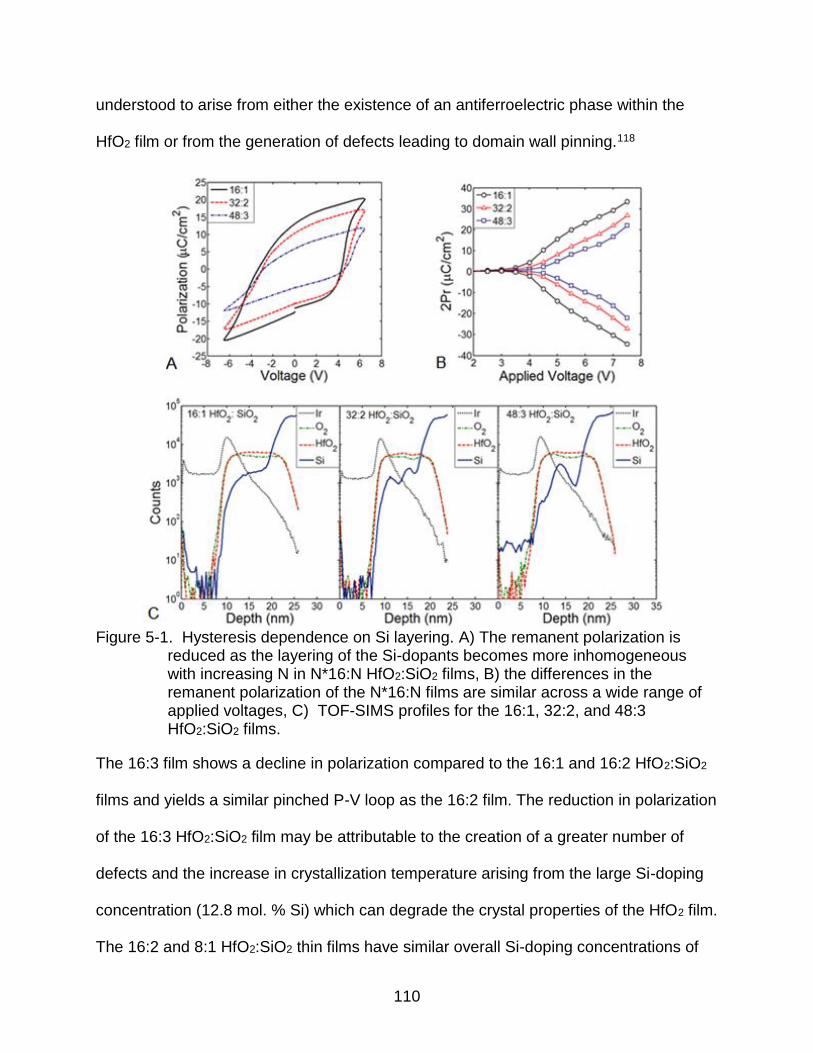
110
understood to arise from either the existence of an antiferroelectric phase within the
HfO2 film or from the generation of defects leading to domain wall pinning.118
Figure 5-1. Hysteresis dependence on Si layering. A) The remanent polarization is
reduced as the layering of the Si-dopants becomes more inhomogeneous with increasing N in N*16:N HfO2:SiO2 films, B) the differences in the remanent polarization of the N*16:N films are similar across a wide range of applied voltages, C) TOF-SIMS profiles for the 16:1, 32:2, and 48:3 HfO2:SiO2 films.
The 16:3 film shows a decline in polarization compared to the 16:1 and 16:2 HfO2:SiO2
films and yields a similar pinched P-V loop as the 16:2 film. The reduction in polarization
of the 16:3 HfO2:SiO2 film may be attributable to the creation of a greater number of
defects and the increase in crystallization temperature arising from the large Si-doping
concentration (12.8 mol. % Si) which can degrade the crystal properties of the HfO2 film.
The 16:2 and 8:1 HfO2:SiO2 thin films have similar overall Si-doping concentrations of

111
9.55 and 9.42 mol. % Si respectively, yet the 8:1 film does not exhibit a pinched P-V
loop (Figure 5-2 A)). The effects of inhomogeneous layering in the 16:2 are thought to
have brought about a larger number of defects, though the formation of an
antiferroelectric phase cannot be excluded. The 16:1 and 8:1 films show similar
ferroelectric properties and have an apparent continuous distribution of Si-dopants with
little local variation as observed within the spatial resolution of the TOF-SIMS. The high-
resolution high angle annular dark field (HAADF) STEM images shown in Figure 5-3
confirm the crystallization of the as-deposited amorphous HfO2:SiO2 films during the
RTA. It is worth noticing that the 16:1 film (Figure 5-3 A)) exhibits a larger grain size and
smoother interfaces with the Ir top electrode and Si substrate, in comparison with the
48:3 film (Figure 5-3 B)), which can be attributed to the less homogeneous layering in
the 48:3 film.
Figure 5-2. Changing the Si concentration and the ALD cycle ratio both show changes
in the hysteresis characteristics. A) The 16:1 and 8:1 films exhibit similar ferroelectric properties, B) increasing N in the 16:N films leads to a pinching of the P-V loop and a diminution of the remanent polarization when N = 3.
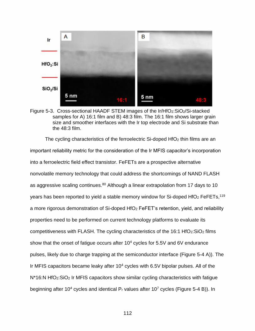
112
Figure 5-3. Cross-sectional HAADF STEM images of the Ir/HfO2:SiO2/Si-stacked
samples for A) 16:1 film and B) 48:3 film. The 16:1 film shows larger grain size and smoother interfaces with the Ir top electrode and Si substrate than the 48:3 film.
The cycling characteristics of the ferroelectric Si-doped HfO2 thin films are an
important reliability metric for the consideration of the Ir MFIS capacitor’s incorporation
into a ferroelectric field effect transistor. FeFETs are a prospective alternative
nonvolatile memory technology that could address the shortcomings of NAND FLASH
as aggressive scaling continues.80 Although a linear extrapolation from 17 days to 10
years has been reported to yield a stable memory window for Si-doped HfO2 FeFETs,119
a more rigorous demonstration of Si-doped HfO2 FeFET’s retention, yield, and reliability
properties need to be performed on current technology platforms to evaluate its
competitiveness with FLASH. The cycling characteristics of the 16:1 HfO2:SiO2 films
show that the onset of fatigue occurs after 104 cycles for 5.5V and 6V endurance
pulses, likely due to charge trapping at the semiconductor interface (Figure 5-4 A)). The
Ir MFIS capacitors became leaky after 104 cycles with 6.5V bipolar pulses. All of the
N*16:N HfO2:SiO2 Ir MFIS capacitors show similar cycling characteristics with fatigue
beginning after 104 cycles and identical Pr values after 107 cycles (Figure 5-4 B)). In

113
contrast, the 16:2 and 16:3 HfO2:SiO2 Ir MFIS films show improved resistance to fatigue
and little variation of Pr over 107 cycles (Figure 5-4 C)), although the maximum Pr of the
films are ~ 5μC/cm2 or less at an applied voltage of 5.5V. The pinching of the P-V loop
in the 16:2 and 16:3 films may be influencing the cycling characteristics.
Figure 5-4. Cycling characteristics of layered Si-doped HfO2 thin films. A) The cycling
characteristics of the 16:1 HfO2:SiO2 Ir MFIS capacitor for various applied voltages, B) for the N*16:N, N = 1, 2, 3 capacitors at 5.5V, C) and for the 16:N, N = 1, 2, 3 at 5.5V which show less reduction in Pr with cycling for N = 2 and 3.

114
It should be noted that a HfO2 thin film doped with 2.08 mol. % Si incorporated
into the Ir MFIS structure yielded no discernible ferroelectric response and a Pr value
less than 1μC/cm2; hence, it is thought that the observed Pr values measured across
the devices are primarily due to intrinsic effects such as switched charge originating
from a ferroelectric phase within the HfO2 thin film, though the influence of defect
dipoles cannot be excluded. The cycling results for the layered Si-doped HfO2 MFIS
capacitors suggest a lifetime of approximately 10,000 - 100,000 cycles, similar to NAND
FLASH22, if the layered stacks are incorporated into operational FeFET devices.
Moreover, the metal-oxide interface provided by IrOx may act as a sink for oxygen
vacancies and improve the cycling characteristics in FeFET. Mueller et al.120
demonstrated that FeFET devices with a Si-doped HfO2 ferroelectric film and TiN
electrodes had robust endurance characteristics up to 104 cycles, after which charge
trapping closed the memory window. Cycling dependent breakdown events, often
reported for ferroelectric HfO2-based MFM devices,89,90,92 were not observed for applied
voltages up to 6V after 107 cycles in the Si-doped HfO2 thin films integrated into the Ir
MFIS device structures.
5.4 Conclusion
Adjusting the Si-dopant distribution within the HfO2 thin films at a ~5.5 – 5.7 Si
mol. % resulted in alterations in the remanent polarization, with increasing
inhomogeneity of the Si-dopants leading to a reduction in Pr. Higher doping
concentrations lead to pinched P-V loops in the Ir MFIS capacitor, formed from either
defect domain pinning or the formation of an antiferroelectric phase. A pinching of the P-
V loop was found to be dependent on both the layering of the Si-dopants within the film
stack and the overall Si doping concentration. Endurance cycling suggests the onset of

115
fatigue at about 104 cycles for the 16:1, 32:2, and 48:3 HfO2:SiO2 layered thin films in
the Ir MFIS device structure. MFIS capacitors with pinched P-V loops were more
resistant to decreases in Pr with voltage cycling. All of the MFIS devices exhibited no
cycling dependent breakdown up to a voltage of 6V and 107 cycles. The Si-dopant
distributions reported here may be used to reduce the depolarization field in FeFET
devices for nonvolatile memory applications.

116
CHAPTER 6 TaN INTERFACE PROPERTIES AND ELECTRIC FIELD CYCLING EFFECTS IN Si-
DOPED HfO2 THIN FILMS3
6.1 Background
Growing reports on HfO2-based ferroelectric thin films20,39,40,44,45,50,106,121 are
striking renewed interest in ferroelectrics for memory applications63,66,120 and energy
storage.69 Si-doped HfO2 thin films were the first ferroelectric HfO2-based thin films
reported with Boscke et al. showing that the crystallization of the Si:HfO2 thin films in the
presence of a capping TiN electrode can lead to the emergence of ferroelectric and
antiferroelectric properties.20 Robust retention characteristics of Si-doped HfO2
ferroelectrics are promising for ferroelectric random access memory (FRAM)
applications.89 Further investigations into ferroelectric Si-doped HfO2 thin films have
illustrated the wide variety of process conditions which can influence the ferroelectric
and electrical properties of Si-doped HfO2, such as the choice of capping electrode,115
the influence of the HfO2 film thickness,122 and the effects of Si-dopant layering.123 In
addition, the recent observation of ferroelectric domains through piezoresponse force
microscopy in Si-doped HfO2 thin films distinguishes its behavior from electrets and
electrochemical responses.124
Due to the very small thicknesses (sub - 10 nm) in which ferroelectricity can be
achieved in Si-doped HfO2, the role of the electrodes and the electrode-ferroelectric
interfaces on the ferroelectric behavior in the thin films cannot be overstated. Si-doped
HfO2 thin films with TiN electrodes have been shown to exhibit the so-called ‘wake-up’
Reprinted with permission from P.D. Lomenzo, Q. Takmeel, C. Zhou, C.M. Fancher, E. Lambers, N.G. Rudawski, J.L. Jones, S. Moghaddam, and T. Nishida, J. Appl. Phys. 117, 134105 (2015). DOI: 10.1063/1.4916715. Copyright 2015, American Institute of Physics.

117
effect in which the remanent polarization increases and the internal electric field
decreases with electric field cycling.82 Zhou et al.82 ascribed this effect to the difference
in charge carrier concentrations between the bottom and top TiN electrodes whereby
the removal or redistribution of mobile charge during bipolar cycling was believed to
subsequently decrease the internal electric field and de-pin ferroelectric domains,
although direct evidence of the chemical nature of the bottom and top TiN electrodes
was not presented. The stability of the two ferroelectric polarization states, a
prerequisite for nonvolatile memory applications, deteriorates with the existence of an
internal or depolarization electric field. The term depolarizing field is used to signify the
specific case when an internal electric field destabilizes a given polarization state. The
term internal electric field (or internal bias) is employed more generally to describe the
shifted ferroelectric characteristics along the electric field axis, often referred to as
imprint, which stabilizes one polarization state at the expense of the other. Since doped
ferroelectric HfO2 thin films are being pursued to increase the memory density of
FRAM55 and to establish the scalability of ferroelectric field effect transistors (FeFETs),63
the presence of a depolarizing field is highly undesirable. In addition, antiferroelectic-like
characteristics observed in HfO2-based films could be related to internal bias fields,74
but no direct evidence has been established yet. Understanding the origin of the internal
electric field and the effects of electric field cycling in doped ferroelectric HfO2 thin films
thus remains an important task from a scientific and technological perspective.
It is known that large surface electric fields originating from the spontaneous
polarization of ferroelectrics cause band bending and ionization of trap states at the
ferroelectric-electrode interface.78,79,94 Brennan78 points out several important factors

118
which influence the space charge distribution and the depolarization field in ferroelectric
thin films. First, ionization of trap states at the ferroelectric-electrode interface will
continue to increase until the surface space charge can effectively screen the internal
polarization of the ferroelectric; it is through the unequal distribution of space charge
between the top and bottom electrode interfaces which then gives rise to a depolarizing
field. Secondly, the metal electrodes form Schottky contacts which provide a sheet of
electrons at the electrode interface to maintain charge neutrality with the positive space
charge region established on the ferroelectric side of the junction. Lastly, the space
charge profile at the ferroelectric/electrode interfaces is influenced by the ferroelectric
polarization, Schottky potential, and the applied electric field.
From the above arguments, it is clear that any investigation into the origin of an
internal electric field observed in ferroelectric thin films should begin at the
electrode/ferroelectric interfaces. To this end, x-ray photoelectron spectroscopy (XPS) is
used to characterize the chemical properties of the top and bottom electrode interfaces
of TaN metal-ferroelectric-metal capacitors which exhibit a large internal bias. The as-
grown ferroelectric domains present in the film are shown to be oriented upward away
from the bottom TaN electrode. Electric field cycling reduces the internal bias, increases
the remanent polarization (Pr), and decreases the relative permittivity, but is not
sufficient to obtain symmetric ferroelectric properties. Since this ‘wake-up’ effect has
been proposed to originate from the asymmetry in the bottom and top electrodes82 and
such a large internal bias has not been seen in HfO2-based devices with symmetric
electrode materials, direct evidence of the chemical behavior of the electrode interfaces

119
between TaN and Si-doped HfO2 provides timely insight into the growing body of
knowledge for thin film HfO2-based ferroelectrics.
6.2 Experiment
TaN bottom electrodes (BE) approximately 8.5 nm thick were RF sputtered on a
highly doped (.001 - .005 Ω-cm) (100) p-Si substrate which had undergone a buffered
oxide etch (BOE, 6:1, 40% NH4F:49% HF in H2O). The BOE was used to etch the native
SiO2 layer from the Si-substrate to reduce the bottom contact resistance before the TaN
BE deposition. After TaN BE deposition, a 10 nm thick HfO2:SiO2 layered film was
grown using plasma enhanced atomic layer deposition (PEALD) with a substrate
temperature of 200°C. Tetrakis(dimethylamido)hafnium and Tris(dimethylamino)silane
were used as the HfO2 and SiO2 precursors respectively. Time of flight - secondary ion
mass spectrometry (TOF-SIMS) and XPS were used to determine the Si mol. % of the
HfO2 thin films corresponding to 24:1 and 16:1 ALD cycling ratios of HfO2 and SiO2. The
Si content was determined to be 1.2 and 1.6 Si mol. % respectively. XPS and TOF-
SIMS was found to be within 0.1 mol. % agreement. TOF-SIMS quantification of Si was
achieved using standards which were created through ion implantation of Si into HfO2.
TOF-SIMS analyses were conducted using a TOF-SIMS V instrument equipped with a
Binm+ (n = 1 - 5, m = 1, 2) liquid metal ion gun. Approximately 8.5 nm thick TaN top
electrodes (TE) were RF sputtered on the Si-doped HfO2 thin films. Unless specified
otherwise, the 1.2 and 1.6 mol. % Si-doped HfO2 thin films were annealed at 700 °C
and 800 °C for 20 s respectively in nitrogen to crystallize the Si-doped HfO2 thin films.
100 nm thick Ir contacts were then sputtered and subsequently lifted off to serve as a
hard mask. Wet etching was carried out with a 6:1.1:1 (H2O:H2O2:NH4OH) SC1 solution
120
at 65°C, a similar recipe has been reported to yield a greater than 100:1 selectivity
between TaN:HfO2.125 The patterned capacitors are 10,000μm2.
In previous work,115,123 the Si concentration was measured in
metal/HfO2:Si/SiO2/Si capacitors where it was witnessed that Si diffusion into the HfO2
film from the substrate which led to a larger incorporated Si concentration. Furthermore,
the lack of a clear boundary between the likely formation of a hafnium silicate layer at
the HfO2/SiO2 interface in metal/HfO2:Si/SiO2/Si structures, the inhomogeneous nature
of the Si-doping profile, and the weak sensitivity factor of Si relative to Hf and O in XPS
makes quantification of small concentrations of Si in thin film HfO2 nontrivial. Hence, it is
believed to be helpful to provide the ALD cycling ratio which was used to fabricate the
HfO2:Si thin films since the ferroelectric characteristics can also be tuned through the Si-
dopant layering profile.123 It should be pointed out that Mueller et al.105 used a 16:1
HfO2:SiO2 ALD cycling ratio which achieved 3.8 mol. % Si where in this work only 1.6
mol. % Si is observed in the films; however, variations in the actual Si concentration for
a given ALD cycle ratio can be expected due to different deposition tools, deposition
temperatures, and oxidizers to name just a few factors.
Hysteresis measurements were carried out on the metal-ferroelectric-metal
(MFM) capacitors with a Sawyer-Tower circuit at 1 kHz to obtain the polarization –
electric field (P-E) plots. An Agilent 4294A was used to take capacitance-voltage (C-V)
measurements with an AC signal amplitude of 50mV at 50 kHz to extract the relative
permittivity characteristics of the Si-doped HfO2 thin films. Voltage cycling was
performed with bipolar square waves at 1 kHz and the terms ‘unpoled’ and ‘pulse poled’
will be used to describe ferroelectric films before and after cycling respectively. Unless

121
specified otherwise, all bipolar cycling was performed with an electric field magnitude of
3.5 MV/cm. Pulsed transient current measurements were carried out with an Agilent
33511B waveform generator with a 50 Ω resistor in series with the ferroelectric
capacitor. Electrical pulses during the extracted switching current transients had a 100
ms delay time. All electrical measurements were performed with the bottom electrode
grounded.
XPS was carried out through a Phi 5000 Versaprobe II with a monochromated Al-
Kα source (1486.6 eV), an exit angle of 45°, a pass energy of 23.5 eV, and the
spectrum was aligned by putting the C1s binding energy at 284.8 eV. The XPS analysis
beam spot size was 200 μm in diameter. In-situ depth profiling during XPS was
achieved using an Ar+ gun with an accelerating voltage ranging from 0.5 keV to 3.0 keV.
Grazing incidence X-ray diffraction (GIXRD) patterns were measured using a Rigaku
Smartlab diffractometer with a 0.5° angle of incidence. GIXRD patterns were measured
from 10 to 95° 2θ with a step size of 0.05° and a 2 s/step counting time. High-resolution
cross-sectional transmission electron microscopy (HR-XTEM) was used to investigate
the structure of the capacitors and measure the thicknesses of the different layers using
a JEOL 2010F transmission electron microscope operated at 200 kV and equipped with
a Gatan Orius SC200B digital camera. HR-XTEM specimens were prepared using an
FEI DB235 scanning electron microscope/Ga+ focused ion beam system using methods
described elsewhere;126–129 care was taken to minimize sidewall damage to the
specimens by performing the final milling steps using a 5 kV Ga+ beam.130,131 The
specimens were prepared such that the thin dimension (foil normal) corresponded to an

122
in-plane <110> direction; during HR-XTEM imaging, the specimen was oriented such
that the incident beam was aligned to this direction.
6.3 Results and Discussion
The hysteresis loop of the Si-doped HfO2 thin films with TaN electrodes is shifted
in the positive direction along the electric field axis as can be seen in Figure 6-1. The
coercive field is usually determined by the electric field values for which the polarization
becomes zero in the P-E curve. For as-fabricated devices, a coercive field of .85 MV/cm
was extracted from the P-E curve while an approximately 1.2 MV/cm coercive field was
obtained for both Si-doped HfO2 thin films after electric field cycling. The cycled film’s
coercive field is higher than the coercive field value of ~ 1 MV/cm first reported for Si-
doped HfO2 ferroelectric thin films with TiN electrodes.20 Alternatively, the coercive field
can be determined by the peaks in the switching current which in our case results in a
larger coercive field of 1.4 MV/cm for the pulse poled ferroelectric films. Since the
switching current peaks in the unpoled ferroelectric capacitors have coercive values of
1.3 MV/cm and are in much closer agreement with the pulse poled device, the current
transient method yields a more consistent determination of the coercive field value
which is not expected to change in magnitude with electric field cycling. Schenk et al.
has provided a review on the usefulness of the transient current analysis during
hysteresis measurements.74 The negative coercive field in the as-fabricated ferroelectric
capacitors is ~ 0 MV/cm as seen clearly in the negative switching current peaks in
Figure 6-1 A) and C). An internal electric field, EI, (2) is produced from the significant
asymmetry in the negative and positive coercive fields.
2
cc
I
EEE (6-1)

123
The unpoled Si-doped HfO2 thin films with TaN electrodes exhibit a 1.3 MV/cm
internal electric field. Furthermore, the positive Pr value is ~ 0 µC/cm2 which indicates
that the as-grown ferroelectric domains are aligned in one direction pointing toward the
top electrode. The situation can be illustrated by looking more closely at the current
transients in Figure 6-1 A) and C). As the ferroelectric is being excited by the clockwise
triangle wave during hysteresis, the switching current peak occurs at about 2.6 MV/cm
during the ramp upward. However, on the return to 0 MV/cm, the ferroelectric Si-doped
HfO2 thin film already begins switching back to its original state. Hence, there is only
one stable polarization state in the as-fabricated ferroelectric Si-doped HfO2 thin film
because of the overwhelming depolarization field domains encounter when they point
downward toward the bottom electrode. Electric field cycling reduces the internal
electric field to ~ 0.6 MV/cm in the Si-doped HfO2 thin films after 10,000 bipolar cycles
and increases both positive and negative remanent polarization values.
Similar to the observations made by Zhou et al.,82 a logarithmic increase in the
remanent polarization during electric field cycling is observed, Figure 6-2 A)-B), given by
NAPP rr log0 (6-2)
where Pr0 is the initial remanent polarization, A is the acceleration factor, and N is the
number of bipolar cycles. The acceleration factor is larger for the positive remanent
polarization and increases for stronger applied electric fields. The negative acceleration
factor remains constant regardless of the magnitude of the electric field. The
acceleration factors extracted from the logarithmic fits are given in Table I. The
simultaneous decrease in the internal electric field and increase in remanent

124
Figure 6-1. Hysteresis of the 1.2 mol. % Si films before A) and after B) 10,000 bipolar
cycles illustrates the large increase in Pr and reduction of the internal bias. The 1.6 mol. % Si doped-HfO2 thin films exhibit the same characteristics before C) and after D) cycling, but has a slightly larger background leakage current relative to the current switching peaks due to the higher anneal temperature. Both as-fabricated films have a negative coercive field ~ 0 MV/cm and a positive remanent polarization of ~ 0 µC/cm2, indicating that the as-grown ferroelectric domains are pointing upward away from the TaN bottom electrode.
polarization lends support to the hypothesis that the redistribution or compensation of
electrically charged defects is occurring with bipolar cycling. Moreover, the strong
dependency of the positive acceleration factor on the magnitude of the electric field
suggests that the redistribution of charged defects or defect dipoles is occurring more
strongly at one electrode interface in the ferroelectric Si-doped HfO2 thin film with
electric field cycling.

125
Table 6-1. Acceleration factors for the Si-doped HfO2 thin films. 1.2 mol. % Si 1.6 mol. % Si
Electric Field (MV/cm) A+ (μC/cm2) A- (μC/cm2) A+ (μC/cm2) A- (μC/cm2)
3.0 .334 -.234 .431 -.309 3.5 .521 -.251 .712 -.317 4.0 .676 -.236 .890 -.310
Figure 6-2. The change in the remanent polarization for the A) 1.2 mol. % Si-doped and the B) 1.6 mol. % Si-doped HfO2 thin films exhibit a logarithmic dependence with electric field cycling, experimental data is given by the symbols and the logarithmic fits are given by the solid line. A change in the slope before breakdown indicated an increase in the leakage current contribution toward Pr and is given by a dashed line. Changes in εr for both Si compositions C)-D) show the switching peaks shifting left and on overall decrease in relative permittivity with electric field cycling.

126
The crystal structure of the Si-doped HfO2 thin films is consistent with the
tetragonal or Pca21 orthorhombic phase116 as confirmed by GIXRD (Figure 6-3). The
polar orthorhombic Pca21 space group was originally invoked to explain the emergence
of ferroelectric behavior in Si-doped HfO2 thin films.20 Theoretical work has shown that
two polar orthorhombic space groups, Pca21 and Pmn21, have very close free energies
and can be formed through a distortion of the nonpolar tetragonal P42/nmc phase along
the [001] and [100] directions respectively.116 The concurrent increase in Pr and
decrease in εr during electric field cycling is supportable by such a phase
transformation, whereas the growth of an interfacial layer during pulsed poling would fail
to explain the increase in Pr.
Figure 6-3. GIXRD of the Si-doped HfO2 thin films shows the crystal structure to be
consistent with the tetragonal or orthorhombic phase for both compositions.
Up to this point the asymmetry in the ferroelectric characteristics still remains
unexplained. As was noted in the introduction, the existence of an internal electric field
is due to the unequal space charge densities at the top and bottom
127
electrode/ferroelectric interfaces. Motivated by this understanding, XPS was used to
evaluate the chemical behavior of the TaN TE and BE interfaces on the Si-doped HfO2
thin films. Due to the very high selectivity (100:1) of the SC1 wet chemistry with respect
to TaN and HfO2,125 the wet-etched surface provides an excellent snapshot of the
TaN/HfO2 top electrode (TE) interface composition. Henceforth, the SC1 wet etched
surface will be referred to as the TE interface. Interestingly, a significant presence of Hf-
N bonds is present at the TE interface as seen by the low energy shoulder in the Hf 4f
binding energy Figure 6-4 A). A low intensity tantalum and nitrogen signal was also
picked up at the TE interface during XPS. High resolution XPS scans show that the
residual tantalum on the surface is primarily metallic (Ta0) with only a small fraction of
Ta-N bonds contributing to the Ta 4f binding energy at the TE interface, Figure 6-4 B).
Both Ta 4f and Hf 4f consist of a 4f 7/2 and 4f 5/2 spin doublet which gives rise to two
peaks for each chemical species. The N 1s binding energy shows contributions from
both N-Hf and N-Ta bonds, Figure 6-4 C). There are more N-Hf bonds than N-Ta bonds
on the wet-etched TE interface, as seen by the greater contribution of N-Hf to the N 1s
binding energy. The atomic concentration of tantalum at the TE interface is less than
4%, its detected presence after the SC1 wet etch is likely due to diffusion during the
RTA and decomposition of interfacial TaN into Ta0 and HfN. It should be noted that
metallic Ta0 has a lower etch rate than TaN for the SC1 chemistry, and since both Ta
and TaN SC1 etch rates are larger than HfO2, the TaN/HfO2 interfacial surface
composition is preserved without any contribution from the bulk of the TaN top
electrode.

128
Using an Ar+ ion beam during XPS, the Si-doped HfO2 thin films were etched
down to the bottom electrode (BE) interface to determine the chemical heterogeneity of
the BE and TE interfaces. The Hf 4f binding energy at the BE interface confirms that Hf-
N bonds are again present, Figure 6-4 D). Significantly, the Ta 4f binding energy at the
bottom electrode interface shows the presence Ta-O bonds, Figure 6-4 E), thus
verifying that the bottom electrode TaN interface is oxidized. The exact oxidation state
of Ta cannot be resolved, but TOF-SIMS yielded the most ionized molecular fragments
for TaO2 and Ta2O5 respectively.
Figure 6-4. XPS analysis of the TE interface shows A) Hf-N bonds in Hf 4f, B) residual
metallic Ta0 in Ta 4f, and C) both N-Hf and Ta-N bonds in N 1s. The BE interface shows D) Hf-N bonds in Hf 4f, E) Ta-O bonds in Ta 4f, and F) N-Hf and and N-Ta bonds in the N 1s binding energy.

129
The presence of metallic Ta0 and Hf-N bonds suggest decomposition of TaN at the BE
interface during ALD or the rapid thermal anneal. The N 1s binding energy of the BE
interface shows a greater degree of N-Ta bonds than N-Hf bonds, Figure 6-4 F).
The observed N-Hf bonds at both electrode interfaces, in which the nitrogen
atom substitutes for oxygen in the lattice, will effectively neutralize the gap states
caused by oxygen vacancies and raise the valence band maximum by 0.2 eV.132,133
Umezawa et al. found that when two nitrogen atoms occupy the nearest neighbor
oxygen sites next to a neutral oxygen vacancy (VO), each nitrogen atom extracts an
electron and produces a positively charged oxygen vacancy (VO2+).132 The addition of
an electron to the two neighboring nitrogen atoms and the resulting production of a
positively charge oxygen vacancy thus forms an electric dipole.132 Since both electrode
interfaces contain substitutional nitrogen atoms at concentrations greater than 10
atomic %, positively charged oxygen vacancies and the resulting N-V02+-N dipole
complexes are expected to be present in the films. Moreover, the redistribution of the
positively charged oxygen vacancies and subsequent reorientation or randomization of
the N-V02+-N dipole complexes can explain the electric field cycling behavior in the Si-
doped HfO2 thin films. Since the bottom TaN interface is oxidized, the aggregation of
VO2+ at the BE interface will not be adequately screened by the sheet of electrons in the
metal due to the physical separation interposed by the TaxOy layer.
The situation can be visualized in Figure 6-5. The internal bias present in the Si-
doped HfO2 thin films is caused by the accumulation of positively charged oxygen
vacancies at the BE. Since the positively charged oxygen vacancies are not adequately
screened at the oxidized TaN BE interface, the as-grown ferroelectric domains are
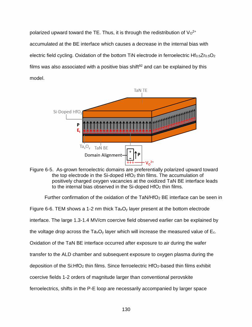
130
polarized upward toward the TE. Thus, it is through the redistribution of VO2+
accumulated at the BE interface which causes a decrease in the internal bias with
electric field cycling. Oxidation of the bottom TiN electrode in ferroelectric Hf0.5Zr0.5O2
films was also associated with a positive bias shift92 and can be explained by this
model.
Figure 6-5. As-grown ferroelectric domains are preferentially polarized upward toward
the top electrode in the Si-doped HfO2 thin films. The accumulation of positively charged oxygen vacancies at the oxidized TaN BE interface leads to the internal bias observed in the Si-doped HfO2 thin films.
Further confirmation of the oxidation of the TaN/HfO2 BE interface can be seen in
Figure 6-6. TEM shows a 1-2 nm thick TaxOy layer present at the bottom electrode
interface. The large 1.3-1.4 MV/cm coercive field observed earlier can be explained by
the voltage drop across the TaxOy layer which will increase the measured value of Ec.
Oxidation of the TaN BE interface occurred after exposure to air during the wafer
transfer to the ALD chamber and subsequent exposure to oxygen plasma during the
deposition of the Si:HfO2 thin films. Since ferroelectric HfO2-based thin films exhibit
coercive fields 1-2 orders of magnitude larger than conventional perovskite
ferroelectrics, shifts in the P-E loop are necessarily accompanied by larger space

131
charge densities. Modeling the C-V characteristics after Brennan,78 ionized charge
densities on the order of 1019 – 1020 cm-3 are extracted which are 1-2 orders of
magnitude larger than values extracted from lead zirconate titanate thin films78,79 and
supports the magnitude of the electric field shift observed in the hysteresis loop. It was
found that in Sr-doped HfO2 thin films, the activation energy for ‘wake-up’ cycling and
subsequent fatigue was found to be one order of magnitude lower than perovskites.88
Schenk et al. suggested that the redistribution of oxygen vacancies and defects along
domain or grain boundaries were likely candidates for ‘wake-up’ and fatigue; the lower
activation energies for these phenomena were attributed to the larger applied electric
fields in HfO2-based films compared to perovskite ferroelectrics.88
Figure 6-6. TEM confirms the presence of a ~ 1 nm TaxOy layer at the TaN BE
interface.
To determine if the switching kinetics were influenced by the internal electric field
and the unequal space charge distribution, a variation of the Positive-Up-Negative-
132
Down (PUND) pulse methodology76 utilizing repeating NPU and PND pulse trains were
used to calculate Psw+ and Psw
-, (Eq. 6-3) as a function of pulse width.
dttJP
dttJP
swsw
swsw
)(
)( (6-3)
The switching current densities are extracted from the PU and ND pulse sequences
given by
)()()(
)()()(
tJtJtJ
tJtJtJ
DNsw
UPsw (6-4)
Integrating the switching current density profile yields the switched charge resulting from
the P and N pulses while the transient polarization in the U and D terms is also taken
into account. Since the dielectric response and leakage current are nominally the same
in the PU and ND pulses, these contributions are effectively negated in Eq. 6-4. Thus,
the pulsed transient current method has the advantage of being able to account for the
leakage current, dielectric relaxation, and the charging/discharging currents so that a
precise extraction of the polarization switching current can be made.
Similar to previous observations in ferroelectric Si-doped HfO2 thin films,105 a
logarithmic dependence of switched charge can be seen with pulse width in cycled films
(Figure 6-7 A)), indicating that the thin films obey the nucleation limited switching
model134 whereby reverse nucleation of domains occurs through an ensemble of
independently switching regions with a distribution of switching times. The as-fabricated
films show power-law behavior with pulse-width and have steeper slopes than the poled
devices. The power-law behavior can be attributed to the gradual redistribution of
charged defects in the film during the measurement and is not believed to be an intrinsic

133
property of the switching kinetics within the film. Electric field cycling produces a
substantial increase in the switched polarization. The switching current vs. electric field
profiles for a 50 µs pulse width with a 1 µs rise time can be seen in Figure 6-7 B)-E).
Figure 6-7. Switching properties of the Si-doped HfO2 thin films with TaN electrodes. A) The switching kinetics of the Si-doped HfO2 thin films follow a logarithmic dependence in accordance with the nucleation limited switching model, experimental data is given by the symbols and the logarithmic fits are given by the solid lines. B)-E) The switching current before and after electric field cycling with the 1.2 mol. % and 1.6 mol. % Si-doped HfO2 thin films are given by the dashed and solid lines respectively as discussed in the text. The pulse width is 50 µs with a 1µs rise and fall time.

134
Importantly, a small second switching current transient peak is observed in the as-
fabricated 1.2 mol. % Si-doped HfO2 thin film Figure 6-7 B), dashed line, indicating that
an ensemble of domains have longer switching times when attempting to reverse
nucleate against the internal electric field. This would suggest that the broad tail at the
end of the positive switching current accounts for the switching of domains localized
near the accumulation of positively charged oxygen vacancies and defect dipole
complexes at the bottom TaN electrode. Switching occurs later when reverse nucleation
must overcome the internal electric field, but cycling the capacitor decreases the mean
switching time for domains nucleating under a positive electric field while the switching
time remains unchanged for applied negative electric fields before and after cycling. It
can therefore be concluded that electric field cycling redistributes the defect charge or
defect dipoles away from the TaN BE and permits faster reverse nucleation of domains
at that interface.
Previous reports20,61,122,124 on Si-doped HfO2 thin films have shown
antiferroelectric-like characteristics where the P-E loops were pinched. Pinched
hysteresis loops are observed in the Si-doped HfO2 thin films which were doped with
1.6 mol. % Si and annealed at 700 °C for 20 s, Figure 6-8 A). The current transient
during hysteresis shows that the pinched P-E loop is accompanied by four broad and
relatively low intensity current switching peaks in the four quadrants. This is expected
for an antiferroelectric material74 where two sub-lattices produce oppositely oriented
polarization vectors and result in a net zero spontaneous polarization.135 After electric
field cycling, the hysteresis loop becomes narrow and de-pinched with only one clearly
distinguishable switching peak because the merging of the negative current switching

135
peaks cannot be resolved above the background leakage current, Figure 6-8 B). The P-
E loops in Figure 6-8 are not symmetric because Pr ≈ Pr- and Pr
+ ≈ 0 µC/cm2, indicating
that the defect charge at the bottom electrode is still influencing the antiferroelectric-like
thin film’s behavior. The εr vs. electric field profiles exhibit the double butterfly loop
which is well-known to occur in PZT-based antiferroelectrics.75 Electric field cycling
subsequently suppresses two out of the four εr peaks with an overall decrease in
relative permittivity, Figure 6-8 D). The resulting relative permittivity response to the
electric field after cycling closely resembles the asymmetric switching peaks found in
the ferroelectric Si:HfO2 thin films in Figure 6-2, corroborating evidence that defect
charge is influencing the switching properties of the antiferroelectric-like film.
Furthermore, the two permanent εr switching peaks shift leftward indicating a reduction
in the internal electric field. As noted earlier, the decrease in relative permittivity and the
reduction in the internal bias with electric field cycling could be due to a tetragonal
orthorhombic phase transition as a result of oxygen vacancy electromigration and
reorientation or elimination of defect dipoles which stabilize the ferroelectric phase.
Higher Si-doping concentrations can be used to stabilize antiferroelectric behavior in
thin film Si:HfO2 with little dependence on electric field cycling.124
To overcome the lack of detail in the current transient during hysteresis before
and after electric field cycling, pulsed transient current analysis was used to obtain a
closer look at the switching current vs. electric field profile. As can be seen in Figure 6-8
E), the as-fabricated films exhibit back-switching when a positive electric field is applied.
Back-switching is shown by the minima in the switching current profile and is due to the
transient charge that is switched in the U pulse in the NPU pulse train. The inversion of

136
the polarity of the switching current density in Figure 6-8 E) possibly indicates a change
in the switching kinetics of the transient polarization from the NP and PU pulse
transitions. For this case the switched charge in the U pulse exceeded the switched
charge in the P pulse for a duration of time, although the total switched charged in the P
pulse is larger overall indicating the presence of some ferroelectric domains within the
antiferroelectric-like film. Back-switching current transients have also been observed in
antiferroelectric PbZrO3 thin films.136 Cycling the film resulted in an overall increase in
the forward switching current and the magnitude of the back-switched charge was
reduced.
When negative electric fields are applied to the as-fabricated thin films, back-
switching still occurs which is consistent for an antiferroelectric material since a
ferroelectricantiferroelectric transition will proceed when the applied electric field is
removed. In this case, back-switching is found in the D pulse in the PND pulse train,
where the transient polarization decay after the N pulse leads to domain switching in the
D term. Cycling the film results in the merging of the two distinct negative switching
current peaks and the switched charge increases in magnitude. Furthermore, back-
switching is no longer appreciable in the pulsed current transient for negative electric
fields after electric field cycling. Back-switching is exacerbated when domains have to
reverse nucleate against the internal electric field as seen for applied positive electric
fields in the antiferroelectric-like Si:HfO2 thin films.
Overall, electric field cycling increases the switched charge in the
antiferroelectric-like Si-doped HfO2 films regardless of the polarity of the applied electric
field and results in de-pinching of the hysteresis loop. The redistribution of positively

137
Figure 6-8. With a lower temperature anneal, the 1.6 mol. % Si-doped HfO2 thin films exhibit a pinched hysteresis loop A) which opens up after electric field cycling B). C) Four εr peaks are observed as expected for an antiferroelectric material. D) Cycling the Si:HfO2 film results in the disappearance of two of the εr switching peaks. The switching current density vs. electric field profile shows E) back-switching occurring for the as-fabricated films (dashed line) when nucleation must overcome the internal electric field. After 10,000 bipolar cycles (solid line), back-switching still occurs due to the depolarization field as seen by the minima in the switching current peak. F) Switching currents in the direction of the internal electric field are still subject to back-switching (dashed line), but back-switching is suppressed after 10,000 bipolar cycles (solid line).

138
charged oxygen vacancies and the reorientation or elimination of N-VO2+-N dipole
complexes at the oxidized TaN BE is the most probable cause for the stabilization of the
ferroelectric phase with electric field cycling in the pinched Si-doped HfO2 thin films. It
can be concluded that the prevention of oxidation of the electrode interface, which can
be achieved through in-situ ALD deposition or careful selection of the electrode
materials, is a prerequisite to avoid the development of internal electric fields in doped
ferroelectric HfO2 thin films.
6.4 Conclusion
Ferroelectric Si-doped HfO2 thin films with sputtered TaN electrodes were
observed to have highly asymmetric ferroelectric characteristics due to the existence of
a large internal electric field. Electric field cycling increased the remanent polarization
and reduced the magnitude of the internal bias as a result of the redistribution of
charged defects and defect dipoles. The chemical behavior of the TaN bottom and top
electrode interfaces were analyzed using XPS and it was observed that both interfaces
showed nitrogen incorporation into HfO2 while only the bottom electrode interface was
oxidized. It was deduced that the most likely candidate for the internal electric field was
the aggregation of positively charged oxygen vacancies (VO2+) and N-VO
2+-N dipoles at
the oxidized BE interface. The physical separation between the accumulated positive
charge at the BE interface was inadequately screened by the sheet of electrons in the
TaN electrode because of the TaxOy layer. The inadequate charge screening at the
electrode interface caused the as-grown ferroelectric domains to preferentially polarize
upward away from the bottom electrode.
The larger, field-dependent positive acceleration factor indicated that the
redistribution of positively charged oxygen vacancies and the reorientation or

139
elimination of defect dipole complexes at the BE occurred during electric field cycling.
The simultaneous increase in Pr and decrease in relative permittivity was hypothesized
to indicate structural changes in the Si-doped HfO2 thin film as a result of the
redistribution of the charged defects, notably a distortion of the higher εr tetragonal
P42/nmc phase to the lower εr Pca21 or Pmn21 polar orthorhombic phases. The
switching kinetics showed the films to be governed by nucleation limited switching with
longer nucleation times for domains reverse nucleating against the internal electric field.
Electric field cycling improved the switching times and magnitude of the switched
charge as a result of the redistribution of defect charge and defect dipoles at the BE
interface. Si-doped HfO2 thin films with pinched P-E loops exhibited four permittivity
peaks and were observed to back-switch when having to reverse nucleate against the
internal electric field. Subsequent cycling de-pinched the Si-doped HfO2 thin films,
reduced εr, caused the disappearance of two out of the four relative permittivity peaks,
and increased the amount of switched charge due to the stabilization of the ferroelectric
phase. The stabilization of the ferroelectric phase in ferroelectric capacitors with initially
pinched P-E loops was concomitant with the reduction of the internal electric field due to
the redistribution of charged defects and defect dipoles.
The emergence of internal electric fields arising from the unequal distribution of
space charge at the electrodes can be detrimental to ferroelectric-based nonvolatile
memory technologies because of the resulting instability of one of the polarization
states. From this work it can be concluded that in-situ ALD electrode deposition may be
beneficial to avoid oxidation of the electrode surface or that chemically inert electrode
materials should be chosen to avoid the development of a depolarization field. This

140
work established that the antiferroelectric-like characteristics of Si-doped HfO2 can be
influenced by an internal electric field, but the relationship between internal electric
fields and antiferroelectric-like behavior in HfO2-based films requires further
investigation.

141
CHAPTER 7 FERROELECTRIC Si-DOPED HfO2 DEVICE PROPERTIES ON HIGHLY DOPED
GERMANIUM4
7.1 Background
Ferroelectric HfO2-based thin films are compelling candidates for the realization
of CMOS-compatible ferroelectric field effect transistors (FeFETs) due to the highly
conformal atomic layer deposition (ALD) process and its potential for scaling.63,137
FeFETs remain one of the most intriguing emerging memory technologies due to its
small 1-transistor (1T) memory cell when compared to ferroelectric random access
memory (FRAM) architectures with 1 transistor – 1 capacitor (1T/1C) and 2T/2C cells.1
However, FeFETs have remained an elusive memory technology due to the poor
compatibility of conventional perovskite ferroelectrics on Si and the emergence of strong
depolarizing fields arising from the growth of interfacial layers.62
Recent efforts have demonstrated the feasibility of using Si-doped HfO2 as the
ferroelectric gate in FeFETs.63,120,137 In each of those studies, a SiON interfacial layer
was grown in between the Si substrate and the ferroelectric Si-doped HfO2 thin film to
form a metal-ferroelectric-insulator-semiconductor (MFIS) stack. The SiON interfacial
layer (IL) ultimately leads to control of IL growth during annealing, but this comes at the
cost of increasing the operating voltage.137 Thus, despite the excellent CMOS
compatibility of HfO2-based ferroelectrics on Si, the interfacial layer between the
ferroelectric Si-doped HfO2 thin films and the Si channel still remains a reliability
concern.64
Reprinted with permission from © 2015 IEEE. Reprinted, with permission, from P.D. Lomenzo, Q. Takmeel, C.M. Fancher, C. Zhou, N.G. Rudawski, S. Moghaddam, J.L. Jones, and T. Nishida, Ferroelectric Si-doped HfO2 Device Properties on Highly Doped Germanium, IEEE Electron Device Lett. 3106, 1 (2015). DOI: 10.1109/LED.2015.2445352. Copyright 2015, IEEE.

142
One alternative is to use a different semiconductor material as the template for
the ferroelectric field effect transistor such as Ge which is a candidate for future p-type
FETs due to its high hole mobility.138 High temperature anneals of HfO2 on Ge leads to
less interfacial layer growth than HfO2 on Si 139 and ferroelectric HfO2-based gates
should be able to leverage the improved thermal stability of the Ge interface toward
more robust FeFETs in the metal-ferroelectric-semiconductor (MFS) stack structure.
Aiming in this direction, ferroelectric Si-doped HfO2 thin films on p+ Si and p+ Ge
substrates are compared and demonstrate that ferroelectric HfO2 on Ge exhibits lower
voltage operation similar to TaN/HfO2:Si/TaN metal-ferroelectric-metal (MFM) device
performance. The enhanced device properties of ferroelectric Si-doped HfO2 thin films
on Ge are thus presented as a path forward for the realization of Ge-based ferroelectric
field effect transistors with improved reliability characteristics and low voltage operation.
7.2 Experiment
Highly doped p+ (0.001-0.005 Ω-cm) Si (100) substrates underwent a buffered
oxide etch (BOE) to remove the native SiO2 layer, and (0.008-0.05 Ω-cm) Ge (100) 6°
towards (111) p+ wafers were dipped in 49 wt. % HF. A self-limiting SiO2 layer was
grown in ultrapure ozonized water on the Si substrate. For the TaN metal-ferroelectric-
metal (MFM) stack, 8.5 nm TaN top and bottom electrodes were deposited by RF
sputtering. Si-doped HfO2 thin films were deposited by plasma enhanced atomic layer
deposition (PEALD) at 200 °C using Tetrakis(dimethylamido)hafnium and
Tris(dimethylamino)silane with a 16:1 HfO2:SiO2 layering ratio. The Si content was
measured to be 1.6 mol. % by time-of-flight secondary ion mass spectrometry. All
stacks underwent an 800 °C 20 s post-metallization anneal in N2 to crystallize the Si-
doped HfO2 thin films. 50 nm Pt contacts were sputtered on TaN and served as a hard

143
mask to define the capacitor geometry. High-resolution cross-sectional transmission
electron microscopy (HR-XTEM) was performed to examine the structure of the stacks
using a JEOL 2010F transmission electron microscope. Hysteresis measurements were
carried out at 1 kHz using a Sawyer-Tower circuit with a 220 nF capacitor connected to
the top contact. The switching kinetics were studied with a 50 Ω resistor in series with
the ferroelectric capacitors to extract the switching current profiles and switched charge
as a function of pulse width.
7.3 Results and Discussion
HR-XTEM cross-sectional images show the Ge MFS, TaN MFM, and Si MFIS
stack structures in Figure 7-1. The interface between the crystalline Si-doped HfO2 thin
film and the Ge substrate is atomically abrupt as shown in Figure 7-1 A), with possible
indications of local epitaxial growth as shown by the inset. Local epitaxial growth of
ZrO2, which shares many chemical and structural similarities to HfO2, has been
previously reported on Ge.140 An approximately 1.5 nm thick SiO2 interfacial layer is
seen in the Si MFIS stack shown in Figure 7-1 C). Oxidation of the bottom TaN interface
is also observed in Figure 7-1 B).
The hysteresis characteristics of the three stacks show significant differences in
the properties of the ferroelectric Si-doped HfO2 thin films, Figure 7-2 A). The TaN MFM
exhibits a positive bias shift (imprint) which is due to positively charged oxygen
vacancies at the oxidized TaN bottom electrode interface.77 3.5 V was insufficient to
reverse nucleate domains within the Si MFIS capacitor which resulted in sub-loop
behavior with a small Pr, but the Si MFIS devices reach a Pr of 10 µC/cm2 with an
applied bias of 5.5 V.

144
Figure 7-1. HRTEM cross-sectional images of different device stacks. A) TaN/Si:HfO2/Ge, B) TaN/Si:HfO2/TaN, and C) TaN/Si:HfO2/SiO2/Si stacks. The inset in A) shows that the crystallinity of the Si-doped HfO2 thin film extends to the Ge substrate interface after the crystallization anneal.
Figure 7-2. Ferroelectric characteristics of Si-doped HfO2 on Ge. A) Hysteresis characteristics of the Ge MFS, TaN MFM, and Si MFIS at 3.5V. B) Cycling characteristics at +/- 3.5 V with 1 kHz bipolar square waves.
The Ge MFS ferroelectric characteristics are improved compared to the other two
device stacks with a nearly symmetric hysteresis loop and a Pr of 10 µC/cm2 at 3.5 V.
Cycling characteristics confirm that the Ge MFS devices have stable ferroelectric
characteristics whereas the TaN MFM shows the ‘wake-up’ effect with an increase in Pr
with voltage cycling, Figure 7-2 B). The increase in Pr during wake-up is attributable to
the migration of defect charges from the electrode interfaces and has been
hypothesized to originate from structural changes in the Si-doped HfO2 thin films during
cycling 77. The Si MFIS sub-loop operation during cycling is hindered by fatigue. The

145
maximum number of cycles was limited by breakdown in the Ge MFS and TaN MFM
capacitor stacks.
The ferroelectric behavior in HfO2-based films has been attributed to a polar
orthorhombic (Pca21) phase.20 Grazing incidence x-ray diffraction (GIXRD) of HfO2-
based films has been used to confirm the possible existence of the Pca21 phase in Si
doped HfO2 films, Figure 7-3. The sharp reflections at ~50 and ~55 2θ in MFIS and
MFM films are attributed to the signal from the single crystal quartz sample holder.
Figure 7-3. Grazing incidence x-ray diffraction shows that the Si-doped HfO2 thin films are consistent with the tetragonal or Pca21 orthorhombic phase.
The switching kinetics of the Si-doped HfO2 thin films in the Ge MFS device
follow a logarithmic dependence on pulse width, Figure 7-4 A). Extrapolating to a 100 ns
pulse width at 4 V predicts the switched charge (Psw) to be > 15 µC/cm2 which is
promising for high-speed operation of Ge-based FeFET devices. Furthermore, the lower
voltage needed to reverse nucleate domains in the Ge MFS compared to the Si MFIS
will ultimately lead to lower power operation for Ge based FeFETs incorporating

146
ferroelectric Si-doped HfO2. Improved same state data margins have been observed in
the Ge MFS compared to the Si MFIS for bakes in ambient atmosphere up to 175 °C for
300 s, likely due to improvements in the interfacial layer. Reducing the thickness of the
interfacial layer or preventing it altogether can reduce the depolarization field in
FeFETs. 62 The intrinsically high mobility of p-type Ge FETs may enable HfO2-based
MFS FeFET devices for the next generation of high-density, high performance
nonvolatile memory devices.
Figure 7-4. Switching characteristics of ferroelectric SI-doped HfO2 on Ge. A) The switched charge (Psw) in the Ge MFS capacitor follows a logarithmic trend with pulse width. B) Switching currents in the Ge MFS as a function of rise time (tr) and pulse width (PW) with a 1:10 ratio. Switching current profiles were offset in the time axis from one another.
7.4 Conclusion
Three different device stacks consisting of a Si p+ MFIS, a Ge p+ MFS, and a
TaN MFM were characterized to understand their influence on the ferroelectric behavior
of Si-doped HfO2 thin films. HR-XTEM showed that the Si-doped HfO2 thin films
incorporated into the Ge p+ MFS device showed abrupt interfaces with little interfacial
layer growth. The lack of an interfacial oxide layer in the Ge p+ MFS devices favored a
lower operating voltage when compared to the Si p+ MFIS stack. The ferroelectric Si-

147
doped HfO2 thin films showed promising characteristics on the Ge substrate with nearly
symmetric hysteresis loops, voltage cycling stability, and a Pr of 10 µC/cm2. It is
predicted that Ge FeFETs based on the MFS device characteristics observed in this
study can provide the framework for low-power, high-speed devices with improved
retention characteristics for future nonvolatile memory technologies.

148
CHAPTER 8 MIXED Al AND Si DOPING IN FERROELECTRIC HfO2 THIN FILMS5
8.1 Background
The emergence of ferroelectricity in HfO2-based thin films is remarkable due to
the advancements it may enable for developing and emerging memory technologies
such as ferroelectric random access memory (FRAM) and ferroelectric field effect
transistors (FeFETs).141 Ferroelectric behavior in HfO2-based thin films can be
generated through a suitable combination of doping and annealing conditions.20 Various
dopants have promoted ferroelectricity in HfO2 thin films including Si, Al, Y, Gd, Sr, La,
and Zr.20,38,44,45,49,50,106,115 Atomic layer deposition (ALD) is most frequently used to
deposit HfO2 thin films because of its ability to tailor precise doping profiles123 and its
highly conformal growth process which can enable high aspect ratio device structures.55
Ferroelectric HfO2-based thin films are typically grown in an amorphous state and then
crystallized during a rapid thermal anneal (RTA) with a capping electrode. A capping
electrode during rapid thermal annealing enhances and often facilitates ferroelectric
behavior in HfO2-based thin films.44,45,115
The combination of chemical doping and a mechanically constraining top
electrode is postulated to encourage a tetragonal to orthorhombic (to) phase
transformation during the crystallization anneal.20 A noncentrosymmetric, polar Pca21
orthorhombic phase is the candidate source for ferroelectricity in HfO2 thin films. Atomic
imaging has provided some structural evidence for the existence of this crystal phase,51
Reprinted with permission from P.D. Lomenzo, Q. Takmeel, C. Zhou, C. Chung, S. Moghaddam, J.L. Jones, and T. Nishida, Appl. Phys. Lett. 107, 242903 (2015). DOI: 10.1063/1.4937588. Copyright 2015, American Institute of Physics.

149
although a mixture of phases may be present in polycrystalline HfO2 thin films after
rapid thermal annealing.40 The coexistence of the monoclinic, tetragonal, orthorhombic,
and cubic phases may thus become manifest in doped polycrystalline HfO2 thin films. In
order to maximize the remanent polarization (Pr) of ferroelectric HfO2, the fraction of the
polar orthorhombic crystal phase should be increased within the thin films to enlarge the
magnitude of switched charge.
While ferroelectric Hf0.5Zr0.5O2 is attractive due its simple binary composition and
low thermal budget,40 more flexibility in engineering the properties of HfO2-based
ferroelectrics may be achieved with other dopants. For instance, adjusting the Si-dopant
layering distribution in HfO2 thin films integrated into the metal-ferroelectric-insulator-
semiconductor (MFIS) structure illustrated how the Pr could be lowered by increasing
the distance between the Si layers.123 FeFETs may benefit from the engineering of the
ferroelectric for lower Pr’s because of the consequent reduction in the depolarization
field.62 Furthermore, the small quantity of Al and Si dopants required to induce
ferroelectricity in HfO2 thin films opens up the possibility of placing the dopants within
the HfO2 stack simultaneously. It is shown that mixed Al and Si-doped HfO2 thin films
exhibit a wide range of ferroelectric properties through the placement of the dopant
layers within the HfO2 film.
8.2 Experiment
ALD TiN bottom electrodes 10 nm thick were deposited at 200 °C on highly
doped (0.001–0.005 Ω-cm) (100) p+ Si wafers. Tetrakis(dimethylamido)titanium was used
as the Ti precursor and exposed to N2 plasma during TiN growth. HfO2 thin films doped
with both Al and Si were grown by thermal ALD at 200 °C. The Hf, Al, and Si precursors
used were tetrakis(dimethylamido)hafnium, trimethylaluminum (TMA), and

150
tris(dimethylamino)silane respectively. A 24:1 Hf:(Al, Si) pulse ratio was maintained
where a total of 4 dopant layers were incorporated into the 10 nm thick HfO2 thin films.
Three different distributions of the Al and Si dopant layers within the film stack were
fabricated. The three different dopant distributions may be denoted as Si-Al-Al-Si (0.87
mol. % Al, 0.49 mol. % Si), Al-Si-Si-Al (1.08 mol. % Al, 0.75 mol. % Si), and Al-Si-Al-Si
(1.12 mol. % Al, 0.68 mol. % Si) which represents the placement of the dopant layers
from the bottom-up within the HfO2 film. Time of flight secondary ion mass spectrometry
(TOF-SIMS) was employed to quantify the Al and Si content within the HfO2 thin films.
Approximately 2.4 nm of HfO2 are in between each dopant layer in the as-grown films.
ALD TiN top electrodes 10 nm thick were deposited at 200 °C. In previous work, we had
observed ferroelectric behavior in Si-doped HfO2 with a 24:1 HfO2:SiO2 ALD cycle
ratio.77 Thus, the 24:1 ALD cycle ratio was chosen to investigate mixed Al and Si doping
in HfO2 thin films. The entire TiN metal-ferroelectric-metal (MFM) stack was grown
within the ALD chamber at 200 °C to prevent oxidation of the HfO2/electrode interface.77
The MFM stacks were annealed at 700 °C - 900 °C for 20 s in N2. 50 nm thick Pt
contacts were deposited in a liftoff process and used as a hard mask in an SC1 wet
etch for capacitor geometry formation. The capacitor area was 3,600 μm2.
The hysteresis characteristics, also referred to as polarization vs. electric field (P-
E) plots, of the mixed Al and Si doped HfO2 thin films were extracted from a Sawyer-
Tower circuit with a 220nF linear capacitor and a 1 kHz triangle wave. Virgin device
characteristics were extracted from the average of the first 50 hysteresis
measurements. Endurance cycling was performed at 1 MHz with bipolar square waves
and a 50 Ω resistor in series with the ferroelectric capacitor during cycling. Grazing

151
incidence x-ray diffraction (GIXRD) was performed with a Rigaku SmartLab X-Ray
Diffractometer with a grazing incidence angle of 0.5 °, a .05 ° step size, and a 4 s count
time per step.
8.3 Results and Discussion
Simultaneously doping HfO2 thin films with spatially segregated Al and Si dopant
layers may influence the internal strain of the ferroelectric. The strain in ferroelectric
HfO2 impacts the formation of the ferroelectric o-phase114 and could alter the magnitude
of the coercive field.142 Internal strain within HfO2 can be expected to arise from the
mixed doping in view of the experimentally extracted differences in the HfO2 lattice
volume between pure Al (127.88 Å3) and Si (129.57 Å3) doped HfO2 thin films.142 In-
plane tensile stress is thought to promote the favorable to phase transformation114
and enhance the Pr for ferroelectric HfO2 thin films.
The hysteresis characteristics of the mixed Al and Si doped HfO2 thin films reveal
significant differences in the Pr and overall shape of the P-E loop before and after
electric field cycling at anneal temperatures of 800 °C and 900 °C, Figure 8-1(A)-(D).
The virgin characteristics of the Si-Al-Al-Si doped HfO2 thin films exhibit a Pr of 19
μC/cm2 which increases by ~ 1 μC/cm2 after cycling. The P-E loops of both the Al-Si-Si-
Al and the Al-Si-Al-Si doped HfO2 thin films look distorted horizontally in their virgin state
with a Pr of 13 μC/cm2 and 7 μC/cm2 respectively. Cycling subsequently increases the
Pr in the two films by 2 μC/cm2 and 5 μC/cm2 respectively. Electric field cycling,
sometimes referred to as the “wake-up” effect, has been postulated to increase Pr and
decrease the asymmetry in ferroelectric Si-doped HfO2 through the redistribution of
mobile defect charge (i.e. oxygen vacancies) originating from the electrode
interfaces.77,82 Since the mixed Al and Si doped HfO2 thin films show unequal

152
Figure 8-1. Hysteresis characteristics of the mixed Al and Si doped HfO2 thin films
annealed at 800 °C A) before and B) after 5,000 cycles. Annealing the films at 900 °C for 20 s led to increases in the coercive field in the P-E of C) the virgin and D) cycled capacitors. Cycling was performed with +/- 3.5 MV/cm bipolar square waves at 1 kHz.
enhancements of Pr with electric field cycling, lattice relaxations associated with the
promotion of the o-phase may occur at different rates within the differently doped films.
At 900 °C, the Pr trends amongst the three doping layering distributions remain similar,

153
although a significant increase in the coercive field occurs for all of the films. The
remanent polarization value of ~ 20 µC/cm2 found in these mixed Al and Si doped HfO2
thin films are in good agreement with theoretical simulations of the spontaneous
polarization predicted for the Pca21 phase of 52 ~ µC/cm2, which is expected to be
double the Pr found experimentally.116,142 The mixed Al and Si doped HfO2 thin films
exhibit remanent polarization values comparable to Si-, Al-, and Y-doped HfO2, although
higher Pr values have been reported for Gd and La-doped HfO2 thin films.49
GIXRD was used to confirm that all of the mixed Al and Si doped HfO2 thin films
show the possible existence of the Pca21 orthorhombic phase, Figure 8-2. GIXRD
indicates the coexistence of multiple phases within the doped HfO2 thin films. The full
width at half maximum (FWHM) of the t(111)/o(211) diffraction peak around 30 ° is
largest in the Si-Al-Al-Si and smallest in the Al-Si-Al-Si doped HfO2 thin films. Peak
width broadening of the mixed doped HfO2 thin films supports the hypothesis that the
doping distribution of the Al and Si layers may be influencing the strain of the HfO2 thin
film, although changes in grain size cannot be ruled out. Since the largest peak width
broadening was found in the Si-Al-Al-Si doped HfO2 thin films, these films may have the
greatest amount of microstrain. The sharp reflections in the GIXRD plots at ~ 52 ° are
attributed to the signal from the single crystal quartz sample holder.
The way in which the different dopants are layered within the HfO2 thin films
affect the formation of the orthorhombic phase through the induced strain and
competing phase transformations. Since the Si-Al-Al-Si doped HfO2 thin films exhibit the
highest remanent polarization and the most significant peak broadening, it is likely that
strain is aiding in the stabilization of the orthorhombic phase.

154
Figure 8-2. GIXRD confirms the possible existence of the orthorhombic Pca21 phase in all three of the Al and Si doped HfO2 thin films annealed at 800 °C.
Simulations have shown that the tetragonal P42/nmc phase may transition into the polar
orthorhombic Pca21 through a suitable combination of stress and/or electric field.116 In
particular, the preferential formation of the o-phase in the Si-Al-Al-Si distribution may be
generated through a large in-plane tensile strain due to the smaller Al-doped HfO2
lattice volume compared to the larger Si-doped HfO2 lattice volume.114,142 The doping
distribution of Al and Si in the annealed HfO2 thin films was confirmed with TOF-SIMS,
Figure 8-3. The Gaussian shape of the Si and Al distributions are caused by the limited
depth resolution of TOF-SIMS. The dopant layers are consistent with a monolayer or
sub-monolayer of Al or Si.

155
Figure 8-3. TOF-SIMS depth profiles of the A) Al-Si-Al-Si, B) Al-Si-Si-Al, and C) Si-Al-
Al-Si doped HfO2 thin films annealed at 800 °C.
High resolution cross-sectional transmission electron microscopy (HR-TEM) confirmed
that the Al and Si doped HfO2 thin films were crystallized after annealing, Figure 8-4.
Figure 8-4. HR-TEM image of the Si-Al-Al-Si doped HfO2 thin film after annealing at 850 °C. Lattice fringes can be seen in the polycrystalline TiN electrodes.

156
The Pr dependence on annealing temperature and electric field cycling are
shown for the mixed Al and Si-doped HfO2 thin films in Figure 8-5 A)-D). The Al-Si-Al-Si
doped HfO2 thin films favor a lower anneal temperature and reach a maximum virgin Pr
of ~ 9 μC/cm2 at 700 °C. The Al-Si-Si-Al doped HfO2 thin films reach a maximum virgin
Pr of ~ 14 μC/cm2 at 850 °C. An anneal temperature range from 800 °C – 900 °C yields
the highest Pr values on the order of ~ 20 μC/cm2 in the Si-Al-Al-Si doped HfO2 thin
films with the “wake-up” effect being noticeably absent for the 800 °C and 900 °C
anneals. These trends indicate that the proper selection of annealing conditions to
maximize Pr are highly dependent on the doping distributions employed in HfO2-based
thin films. Endurance cycling characteristics of the Si-Al-Al-Si doped HfO2 thin films
annealed at 800 °C for 20 s are shown in Figure 8-5 D). At 3.5 MV/cm, a Pr greater than
15 μC/cm2 is observed up to 108 until breakdown.
Figure 8-5. Anneal temperature dependence of the A) Al-Si-Al-Si, B) Al-Si-Si-Al, and C)
Si-Al-Al-Si doped HfO2 thin films. The black dots denote the virgin Pr and the red squares represent the Pr after 5,000 cycles at 1 kHz, 3.5 MV/cm. D) Endurance cycling of the Si-Al-Al-Si doped HfO2 thin films annealed at 800 °C for different applied electric fields.

157
Breakdown is accelerated at 4 MV/cm and occurs after 106 cycles. Cycling the mixed Al
and Si doped HfO2 thin film at 3 MV/cm delays breakdown until 109 cycles at the cost of
a lower Pr and the acceleration of fatigue. The cycling characteristics are promising for
memory applications such as FRAM which require a very high number of read and write
cycles. Further optimization of the processing conditions, including the doping and
annealing conditions, are likely to provide greater improvements in the maximum
number of cycles HfO2-based ferroelectrics can withstand before breakdown.
8.4 Conclusion
In summary, HfO2 thin films 10 nm thick were simultaneously doped with Al and
Si with different dopant layering distributions. The resulting ferroelectric properties in the
mixed Al and Si doped HfO2 thin films were dependent on the layering distribution and
the anneal temperature. The influence of strain on the formation of the ferroelectric o-
phase may be supported by differences in peak broadening measured from GIXRD
which was found to be dependent on the Al and Si doping distribution. The Al and Si
doped HfO2 thin films were cycled up to 108 times with an applied electric field strength
of 3.5 MV/cm before breakdown occurred. The ability to engineer the ferroelectric
properties of HfO2 thin films by simultaneously doping HfO2 thin films with multiple
dopant species are thus presented as an accessible route for enhancing HfO2-based
ferroelectrics for a variety of applications.

158
CHAPTER 9 ANNEALING BEHAVIOR OF FERROELECTRIC Si-DOPED HfO2 THIN FILMS
9.1 Background
HfO2-based thin films exhibit ferroelectric and antiferroelectric properties under
various doping and annealing conditions.49,90 Ferroelectricity in HfO2 thin films is
intriguing since it could improve and enable nonvolatile memory technologies such as
ferroelectric random access memory (FRAM) and ferroelectric field effect transistors
(FeFETs). Industry adoption of ferroelectric-based memory technologies has been
relegated to niche applications due to the CMOS incompatibility and poor scaling ability
of conventional perovskite ferroelectric materials despite their low-power operation, fast
read/write speeds, and excellent cycling characteristics (> 1012).52 HfO2-based
ferroelectric thin films may overcome these integration barriers due to its conformal
atomic layer deposition (ALD) process for 3-dimensional capacitor structures,55 sub-10
nm scaling ability, and CMOS compatibility.
Si-doped HfO2 ferroelectric thin films crystallize at relatively high temperatures
from around 650 °C – 1000 °C.89,122 The high anneal temperature may be particularly
suitable for FeFETs since the source/drain junction implantation rapid thermal anneals
(RTAs) may be used to simultaneously crystallize Si-doped HfO2.120 Previous reports
have implemented anneals in this temperature range using coarse increments of
temperature (>100 °C) in a mostly isochronal manner,20,77,89,115,120,122 but a systematic
evaluation of the annealing temperature and duration on the electrical properties of Si-
doped HfO2 thin films has not been reported. The remanent polarization (Pr) of Si-doped
ferroelectric HfO2 thin films is generally enhanced at higher annealing
temperatures.89,122 A more comprehensive study on the annealing dependence of the

159
leakage current and breakdown field of ferroelectric Si-doped HfO2 thin film capacitors
may lead to additional insights.
Electric field cycling effects, such as wake-up and an antiferroelectric-like to
ferroelectric transition, are frequently observed in doped HfO2 ferroelectrics.77,82,88,143
Oxygen vacancies at the electrode interfaces and within the HfO2 thin film are one
candidate for the effects of cycling,77,88,144 although charge compensation and
trapping/detrapping of charge carriers may also influence nucleation at the interfaces.143
The cycling endurance of HfO2-based ferroelectric thin films has tended to be limited by
hard breakdown events55,89,105,144–146 and oxygen vacancies are the prime candidate for
the breakdown behavior. Oxygen vacancy conduction and vacancy filament formation
are well-known phenomena in HfO2-based resistive random access memory (RRAM)
devices.147,148 Cycling stability is a very important metric for ferroelectric memories and
traditional lead zirconate titanate ferroelectrics do not exhibit breakdown despite being
cycled for more than 1012 times.52 Breakdown behavior in HfO2 thin films needs to be
studied in order to improve the cycling properties for memory applications. Since
oxygen vacancy formation will be influenced by the annealing conditions, the
breakdown behavior of ferroelectric Si-doped HfO2 thin films will be affected by the
anneal temperature and duration.
Thus, the electrical and ferroelectric properties of Si-doped HfO2 thin films is
presented as a function of anneal temperature and anneal time. Three different Si
layering ratios are used to probe the influence of the annealing conditions on the
differently layered Si-doped HfO2 thin films. The RTA dependence of the electrical
characteristics of Si-doped HfO2 thin films incorporated into ALD TiN metal-ferroelectric-

160
metal (MFM) capacitors are discussed in detail, readers are referred to related works for
structural details on Si-doped ferroelectric HfO2 thin films.20,77,115,122
9.2 Experiment
10 nm thick ALD TiN electrodes were deposited at 200 °C on highly doped
(0.001–0.005 Ω-cm) (100) p+ Si wafers. N2 plasma was used with
tetrakis(dimethylamido)titanium to grow the TiN electrodes. HfO2:SiO2 ALD thin films 10
nm thick were deposited at 200 °C with O2 plasma using
tetrakis(dimethylamido)hafnium and tris(dimethylamino)silane as the Hf and Si
precursors respectively. HfO2:SiO2 layering ratios of 24:1, 16:1, and 12:1 were used to
produce ferroelectric and antiferroelectric properties in the 10 nm thick HfO2 thin films
which contained 4, 6, and 8 layers of Si respectively. Fabrication of the TiN MFM
capacitors was realized through in situ ALD growth at 200 °C to maintain pristine
HfO2/electrode interfaces.77 Rapid thermal anneals were performed at 700 °C – 900 °C
with durations between 5 s – 60 s in N2. 50 nm thick Pt contacts were patterned in a
liftoff process, then used as a hard mask with an SC1 wet etch to form the capacitors.
Electrical measurements were performed on capacitors with areas of 3,600 μm2 and
14,400 µm2.
A Sawyer-Tower circuit was used with a linear 220 nF capacitor connected to the
grounded conducting substrate during hysteresis measurements. A 1 kHz triangle wave
was delivered to the top contact to extract the hysteresis characteristics of the Si-doped
HfO2 thin films. Hysteresis loops for the virgin or as-fabricated films are extracted from
the average of the first 50 hysteresis measurements. Capacitance – voltage (C – V)
measurements to extract the relative permittivity vs. voltage (εr – V) curves were
undertaken on an Agilent 4294A with an amplitude of 50 mV and a 50 kHz frequency.

161
Cycling was performed with bipolar square waves at 1 kHz with a 50 Ω resistor in series
with the ferroelectric capacitor. Dynamic hysteresis current measurements were also
carried out with a 50 Ω series resistor which replaced the 220 nF sense capacitor.
Leakage current densities and breakdown fields were extracted with a Keithley 4200.
Breakdown field measurements were performed with a 1 V/s sweep rate. A current
density of 250 mA/cm2 was used to define the hard breakdown event.
9.3 Results and Discussion
The ferroelectric properties of Si-doped HfO2 thin films can be highly dependent
on the annealing conditions used and the Si doping.122 Higher anneal temperatures tend
to lead to a larger remanent polarization in Si-doped HfO2 thin films89,115,122 and we
observe a similar trend in the hysteresis characteristics of the Si-doped HfO2 thin films
in Figure 9-1. Pinching of the virgin hysteresis loops occur at 700 °C for both the 24:1
and 16:1 layered thin films. This antiferroelectric-like behavior can be modified with
electric field cycling to increase the remanent polarization and open up the hysteresis
loops. 700 °C was insufficient to crystallize the 12:1 HfO2:SiO2 layered films, as shown
by its paraelectric behavior, but the films become antiferroelectric at anneal
temperatures ≥ 750 °C. The antiferroelectric behavior is relatively stable with cycling in
the 12:1 layered films. Martin et al. also demonstrated the cycling stability of
antiferroelectric Si-doped HfO2 thin films with the highest Si content (~ 8.5 mol. %)
reported in that work.124 The antiferroelectric-like behavior that is present at 700 °C in
the 24:1 and 16:1 layered films transitions to a ferroelectric response at 900 °C,
indicating that an antiferroelectric-like ferroelectric transition occurs with increasing
anneal temperature. Figure 9-2 demonstrates the antiferroelectric-like ferroelectric

162
transition with increasing anneal temperature as seen in the εr switching peaks in the
24:1 HfO2:SiO2 layered thin films.
Figure 9-1. The virgin hysteresis characteristics of the 24:1 and 16:1 HfO2:SiO2 thin films show an antiferroelectric-like to ferroelectric transition for increasing anneal temperature. The paraelectric behavior of the 12:1 HfO2:SiO2 thin films annealed at 700 °C indicates the films are amorphous, while higher temperatures lead to antiferroelectric properties.

163
A merging of the four switching peaks of the double butterfly loop converges into two
switching peaks characteristic of ferroelectrics as the anneal temperature is increased.
In contrast to the more lightly doped HfO2 thin films, the 12:1 films retain antiferroelectric
behavior at 900 °C, although they exhibit greater loss as seen by the increase in the
internal area of the hysteresis loop in Figure 9-1.
Figure 9-2. The relative permittivity of the virgin 24:1 HfO2:SiO2 captures the antiferroelectric-like to ferroelectric transition which occurs with increasing anneal temperature. The four switching peaks in the double butterfly loop merge into two switching peaks from left to right as the anneal temperature is increased.
The Pr of the layered HfO2:SiO2 thin films after wake-up cycling is plotted as a
function of anneal temperature with a 20 s anneal duration in Figure 9-3 A). The 24:1
films have the highest Pr across the entire anneal temperature range compared to the
other film compositions, peaking at approximately 15 µC/cm2 around 850 °C and 900
°C. Since antiferroelectric behavior is more stable in the 12:1 HfO2:SiO2 thin films, the Pr
values are on the order of 1 µC/cm2 except at 900 °C, where the effects of cycling begin
to de-pinch the hysteresis loop. Thus, even Si-doped HfO2 thin films with relatively large
amounts of Si incorporation can begin to exhibit field cycling effects when the anneal
temperature is large enough. Intermediate Pr values are extracted from the 16:1 layered
films and they start to converge with the 24:1 films at 900 °C. The remanent polarization

164
of the Si-doped HfO2 thin films becomes larger with increasing anneal temperature, and
the greater Si content within the HfO2 thin films requires higher anneal temperatures to
avoid antiferroelectric-like characteristics.
Figure 9-3. Electrical and ferroelectric parameters of Si-doped HfO2 with anneal temperature. The A) remanent polarization (Pr), B) breakdown field, and C) leakage current density at 3V for the three layered Si-doped HfO2 thin films as a function of anneal temperature with a 20 s anneal time. The Pr was extracted after 1,000 cycles, whereas the breakdown field and leakage current density were measured on as-fabricated capacitors. Symbols in some cases are larger than the error bars.
The breakdown fields in the Si-doped HfO2 thin films decrease with increasing
anneal temperatures, Figure 9-3 B). The most lightly doped HfO2 thin films exhibit the
lowest breakdown fields across the temperature range with a 4.75 MV/cm maximum at
700 °C and a 4.2 MV/cm minimum at 800 °C. Both the 16:1 and 12:1 layered films
exhibit breakdown fields ≥ 5 MV/cm at anneal temperatures less than or equal to 800
°C, indicating that a greater amount of Si incorporation can improve the breakdown
characteristics of HfO2 thin films for low to moderate anneal temperatures. At 900 °C,
the breakdown fields in all of the Si-doped HfO2 thin films begin to converge, indicating
that increasing the Si-doping may not be a feasible route to enhance the breakdown
characteristics of films annealed at the highest temperature where the Pr tends to
maximized. Thus, the breakdown characteristics and the ferroelectric performance

165
(nominally determined by Pr) improve for low temperature and high temperature anneals
respectively in Si-doped HfO2 thin films.
Leakage current densities of the Si-doped HfO2 thin films increase with anneal
temperature in all of the layered HfO2:SiO2 thin films, Figure 9-3 C). At anneal
temperatures of 700 °C and 750 °C, the leakage current densities of the 12:1 and 24:1
films are nearly the same whereas an improvement of almost 1 – 2 orders of magnitude
is observed in the 16:1 HfO2:SiO2 thin films. At moderate anneal temperatures, the 24:1
films exhibit the highest leakage current densities while the 16:1 films have a leakage
current density two orders of magnitude lower. While increasing the number of Si layers
does not uniformly improve the leakage current densities across the entire anneal
temperature range, greater Si incorporation does result in an overall improvement with
moderate anneal temperatures compared to the most lightly doped Si-HfO2 thin films. At
900 °C, the leakage current densities of all of the Si-doped HfO2 thin films become very
similar.
The lower breakdown field, higher leakage current density, and increased Pr with
higher anneal temperatures in all of these Si-doped HfO2 thin films suggests that the
three parameters may be correlated in these capacitors, which may point to a single
underlying mechanism. The trends suggest that the creation of defects, such as oxygen
vacancies, is promoted with higher anneal temperatures and would certainly lead to a
lower breakdown field and higher leakage current density. Similar trends in Pr and
breakdown behavior were observed when TiN electrodes were replaced by TaN
electrodes, with the latter being hypothesized to more efficiently scavenge oxygen from
HfO2 and thus lead to more oxygen vacancies in Gd-doped HfO2.144 In that work, ab

166
initio simulations were used to confirm that oxygen vacancies may encourage the
stabilization of the ferroelectric phase compared to the paraelectric monoclinic phase.
Therefore, the oxygen vacancy model could very well be applicable to the annealing
temperature trends that we observe in the Si-doped HfO2 thin films whereby an increase
in Pr, due to the greater stabilization of the ferroelectric phase, is attended with a
decrease in breakdown field and larger leakage current densities.
The anneal time dependence of the Pr for the 24:1 HfO2:SiO2 thin films is shown
in Figure 9-4 A). The Pr does not change much from 5 s – 40 s at 700 °C, but the 60 s
anneal doubled the Pr to 10 μC/cm2. Therefore, there may be some benefit to extending
the relatively low 700 °C anneal temperature to 60 s durations and beyond for enhanced
ferroelectric characteristics with a lower thermal budget for the Si-doped HfO2 thin film
system. At 800 °C, the remanent polarization increases from about 10 μC/cm2 to 13
μC/cm2 from 5 s to 40 s anneal durations. Pr peaks at 18 μC/cm2 for a 40 s anneal time
at 900 °C. Overall, the remanent polarization can undergo a 30 % – 50 % change by
varying the anneal time at a given temperature in the 5 s – 60 s range. Longer anneal
times tend to promote a larger Pr in the Si-doped HfO2 thin films.
The breakdown field shows a clear anneal time dependence at 700 °C, but at
higher temperatures no dominant trend with anneal time is present, Figure 9-4 B). The
breakdown field undergoes a small decrease from 5 s – 40 s at 700 °C, but then drops
from approximately 4.7 MV/cm to almost 4.4 MV/cm at 60 s. The breakdown field
generally decreases with anneal time at 900 °C, but at 800 °C the anneal time is a poor
indicator of the breakdown characteristics. Since the anneal temperature is a strong
indicator of the expected breakdown field range, it may serve as a more reliable metric

167
than the anneal times explored in this work. Trends in the leakage current density
versus anneal time, as shown Figure 9-4 C), follow opposing lines as the breakdown
field time dependence. At 700 °C the leakage current density generally increases with
anneal time, whereas no consistent anneal time dependence is observed at higher
anneal temperatures. Therefore, the anneal temperature is a better predictor of the
leakage current density than the duration of the anneal.
Figure 9-4. Electrical and ferroelectric parameters of Si-doped HfO2 with anneal time. The anneal time dependence of the A) Pr, B) breakdown field, and C) leakage current density for 24:1 HfO2:SiO2 thin films at 700 °C, 800 °C, and 900 °C. The Pr was extracted after 1,000 cycles, whereas the breakdown field and leakage current density were measured on as-fabricated capacitors. Symbols in some cases are larger than the error bars.
The anneal time, while not as strongly influential as the anneal temperature, can
substantially affect the remanent polarization, but the leakage current and breakdown
field are largely determined by the anneal temperature in the 800 °C – 900 °C range.
The strongest temporal dependence is found in the relatively low anneal temperature at
700 °C where the increase in Pr, and simultaneous decrease in breakdown field and
higher leakage current density attends the longer anneal durations. Hence, the anneal
time trends, when present, reflect the same overall correlation of the Pr, breakdown
field, and the leakage current density as the trends reflected with anneal temperature.
168
The creation of oxygen vacancies can certainly be expected to be dependent on both
the anneal time and temperature, though the clearer, more consistent trends in anneal
temperature seem to indicate that the RTA temperature plays the dominant role in
determining the ferroelectric and electrical properties in the TiN MFM thin film
capacitors.
Electric field cycling and the ferroelectric properties of Si-doped HfO2 thin films
are affected by the annealing conditions and the Si-dopant layering ratio, as shown in
Figure 9-5. Three unique cases of electric field cycling are identified in the ferroelectric
and antiferroelectric-like capacitors. The pinching of the polarization – electric field (P –
E) loop in as-fabricated 24:1 films annealed at 750 °C open up with electric field cycling,
Figure 9-5 A). Dynamic hysteresis currents confirms that the virgin 24:1 films have four
switching current peaks near or within all four quadrants, indicating that the behavior is
consistent with an antiferroelectric material.74 The four switching current peaks begin to
merge into two dominant switching current peaks with electric field cycling and become
stable at about 1 MV/cm, the coercive field of ferroelectric Si-doped HfO2. Thus,
standard hysteresis measurements and dynamic switching currents indicate that
antiferroelectric characteristics are present in the as-fabricated HfO2 thin films but
undergo a transition to ferroelectric behavior with electric field cycling.
In contrast to the 24:1 HfO2:SiO2 thin films, the 12:1 thin films annealed under the
same conditions exhibit relatively stable antiferroelectric properties with electric field
cycling, Figure 9-5 C)-D). The hysteresis loops of the antiferroelectric thin films undergo
some reduction in pinching and an increase in spontaneous polarization with cycling.

169
Interestingly, the positive and negative switching current peaks move inward towards
lower electric fields with cycling.
Figure 9-5. Three unique cases demonstrating the effects of electric field cycling in the Si-doped HfO2 thin films are shown with the hysteresis and dynamic hysteresis current plots side by side for A) - B) the antiferroelectric-like to ferroelectric transition, C) – D) stable antiferroelectric characteristics, and E) – F) the reduction of imprint in 900 °C 60 s annealed 24:1 layered HfO2:SiO2 thin films.
170
The observed stability in antiferroelectric behavior in the thin films seems to be
related to the higher electric fields needed to cause an antiferroelectric ferroelectric
field transition, where the switching current peaks are further away from the origin and
more distinctly located within the four quadrants of the hysteresis plot. The ferroelectric
24:1 HfO2:SiO2 thin films annealed at 900 °C for 60 s show a small positive bias imprint
in the as-fabricated MFM TiN capacitors, Figure 9-5 E)-F). After just 5 cycles, both
switching current peaks shift leftward by approximately 0.5 MV/cm. Increasing the
number of cycles leads to a split-up in the positive switching current peak to two peaks
whereby the small switching peak at 1 MV/cm becomes dominant and absorbs the
higher field induced positive switching current with increasing cycles. After the initial 5
cycles, the negative switching current peak increases in height but does not change its
location.
Imprint has been hypothesized to originate from the aggregation of positively
charged oxygen vacancies at the oxidized bottom electrode interface in TaN MFM
capacitors,77 and the possibly greater tendency towards oxidation by TaN compared to
TiN electrodes has been linked to larger coercive fields.144 Since two different time-
scales of change in the switching current peaks with electric field cycling occurs, two
separate mechanisms are likely occurring in the TiN MFM capacitors which influence
the ferroelectric switching characteristics. The rapid leftward shift field within the first 5
cycles is unlikely to be generated by the redistribution of oxygen vacancies, but points
to the possibility of trapping and/or detrapping of charge carriers at one or both of the
electrode interfaces. The split-up into two positive switching current peaks and their
gradual merging together over 1,000 cycles may instead be attributable to the
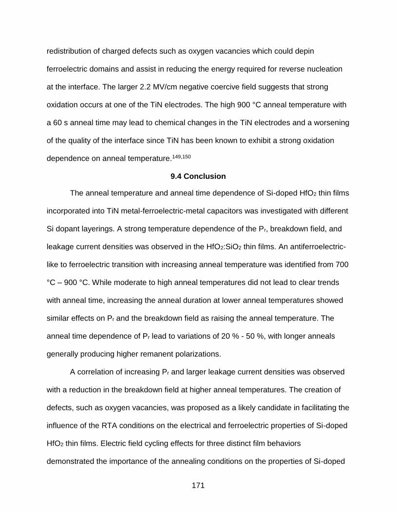
171
redistribution of charged defects such as oxygen vacancies which could depin
ferroelectric domains and assist in reducing the energy required for reverse nucleation
at the interface. The larger 2.2 MV/cm negative coercive field suggests that strong
oxidation occurs at one of the TiN electrodes. The high 900 °C anneal temperature with
a 60 s anneal time may lead to chemical changes in the TiN electrodes and a worsening
of the quality of the interface since TiN has been known to exhibit a strong oxidation
dependence on anneal temperature.149,150
9.4 Conclusion
The anneal temperature and anneal time dependence of Si-doped HfO2 thin films
incorporated into TiN metal-ferroelectric-metal capacitors was investigated with different
Si dopant layerings. A strong temperature dependence of the Pr, breakdown field, and
leakage current densities was observed in the HfO2:SiO2 thin films. An antiferroelectric-
like to ferroelectric transition with increasing anneal temperature was identified from 700
°C – 900 °C. While moderate to high anneal temperatures did not lead to clear trends
with anneal time, increasing the anneal duration at lower anneal temperatures showed
similar effects on Pr and the breakdown field as raising the anneal temperature. The
anneal time dependence of Pr lead to variations of 20 % - 50 %, with longer anneals
generally producing higher remanent polarizations.
A correlation of increasing Pr and larger leakage current densities was observed
with a reduction in the breakdown field at higher anneal temperatures. The creation of
defects, such as oxygen vacancies, was proposed as a likely candidate in facilitating the
influence of the RTA conditions on the electrical and ferroelectric properties of Si-doped
HfO2 thin films. Electric field cycling effects for three distinct film behaviors
demonstrated the importance of the annealing conditions on the properties of Si-doped

172
HfO2 thin films. This study adds growing evidence to the link between the RTA
conditions and the ferroelectric properties of Si-doped HfO2 whereby the creation of
oxygen vacancies and the interaction between the TiN electrodes with the HfO2 thin film
may play a dominant role in the overall behavior of the ferroelectric HfO2 thin films.

173
CHAPTER 10 STUDIES ON FERROELECTRIC AND ANTIFERROELECTRIC HAFNIUM-
ZIRCONIUM OXIDE-BASED THIN FILMS
10.1 Background
The ferroelectric and antiferroelectric characteristics of HfxZr1-xO2 thin films are
interesting because of the complete miscibility of the hafnia-zirconia material
system.12,21,39 Moreover, ferroelectric HfxZr1-xO2 thin films may be particularly suited for
integrated microelectronic applications because of their relatively low crystallization
temperature (400 – 800 °C) and resistance to hydrogen annealing.40,59 It has been
demonstrated that optimal ferroelectric properties tend to occur at the binary Hf0.5Zr0.5O2
composition, whereas increasing the Hf content leads to an increasing presence of the
monoclinic phase and a reduction in the remanent polarization.39 Zr-rich HfxZr1-xO2 thin
films exhibit antiferroelectric behavior and may be used as energy storage
capacitors.39,69
The antiferroelectric properties of Hf0.3Zr0.7O2 showed a promising energy
storage density (ESD) of 30 J/cm3 with a 50 % efficiency over a wide temperature
range.69 A reversible tetragonal orthorhombic field-induced phase transition is
believed to be responsible for generating antiferroelectricity.41 Since it has been found
that Si and Al can encourage the formation of the tetragonal phase,49 doping HfxZr1-xO2
with Al or Si could be a viable route towards improving the antiferroelectric properties of
the thin films. It was shown that antiferroelectric Si-doped HfO2 thin films exhibited up to
a 40 J/cm3 energy storage density with an efficiency of 80 %.71 The potential for using
antiferroelectric Si-doped HfO2 thin films for supercapacitors or infrared sensors was
adequately demonstrated in that work, although the large 1000 °C anneal temperature
will likely prove prohibitive for integrated applications.71 As will be shown in this work,

174
doping HfxZr1-xO2 with Al or Si can enhance the energy storage density and efficiency
without increasing the thermal budget.
The thickness and anneal dependence of ferroelectric Hf0.5Zr0.5O2 has been
previously studied in the context of the remanent polarization and the manifested crystal
phases.40 However, several unresolved points about Hf0.5Zr0.5O2 and its thickness
dependence remain. For instance, the data retention characteristics of Hf0.5Zr0.5O2 thin
films have not been studied. Data retention is the most important reliability metric for a
ferroelectric to be used in a nonvolatile memory technology such as FRAM, thus, an
assessment of any ferroelectric material’s potential for memory applications requires
retention tests. Furthermore, a thickness dependence study on the data retention may
yield additional insight about ultrathin Hf0.5Zr0.5O2 films which may be subject to an
appreciable depolarization field with decreasing film thicknesses.151
While the thickness dependence of Hf0.5Zr0.5O2 is well understood, it is not known
how different compositions of the HfxZr1-xO2 system will be affected by the film
thickness. It is also unclear what effect a spatial gradient in the distribution of Hf and Zr
within HfxZr1-xO2 thin films would have on the ferroelectric properties. Since the critical
grain size for the formation of the tetragonal phase is larger in ZrO2 ( ~ 30 nm) than
HfO2 ( ~ 7 – 10 nm), a compositional gradient which includes a Hf-rich region in
Hf0.5Zr0.5O2 may inhibit the tetragonal phase in ultrathin films. Thus, a study on the size
effect and compositional dependence of HfxZr1-xO2 may help in distinguishing whether
the changes in ferroelectric behavior in ultrathin HfxZr1-xO2 originates from a
depolarization field or in the favorability of the formation of the tetragonal phase.

175
Chapter 10 studies the ferroelectric and antiferroelectric properties of HfxZr1-xO2
and is split into three major sections. The first section will explore the effect of Si or Al
doping of Hf0.5Zr0.5O2 thin films. The second section will investigate the thickness
dependence of Hf0.5Zr0.5O2. The last section will study the thickness dependence of
compositionally graded in HfxZr1-xO2 thin films. Overall, each section yields experimental
results which have important implications for future applications of HfxZr1-xO2 thin films.
10.2 Experiment
Thin film capacitors were fabricated on a highly doped (0.001–0.005 Ω-cm) (100)
p+ Si substrate. The conducting Si substrate was grounded and served as the bottom
contact. Plasma enhanced atomic layer deposition was used to deposit 10 nm thick TiN
bottom electrodes where tetrakis(dimethylamido)titanium was used as the titanium
precursor and exposed to N2 plasma at 200 °C. Hf0.5Zr0.5O2 thin films were grown by
thermal ALD at 200 °C by alternating tetrakis(dimethylamino)zirconium and
tetrakis(dimethylamido)hafnium precursors. HfxZr1-xO2 film thicknesses were calibrated
from the approximately 1 Å/cycle growth rate for each precursor and were confirmed
with TEM. For Al or Si doped Hf0.5Zr0.5O2 thin films, trimethylaluminum (TMA) and
tris(dimethylamino)silane were sued as the precursors respectively. The ALD cycle ratio
of Hf0.5Zr0.5O2:Si was 48:1 and 24:1 which led to the incorporation of 2 and 4 layers of Si
within 10 nm thick Hf0.5Zr0.5O2 films. Al-doped Hf0.5Zr0.5O2 thin films were fabricated with
a 24:1 ALD cycle ratio. Unless stated otherwise, all Hf0.5Zr0.5O2-based thin films
fabricated were 10 nm thick. Compositionally graded HfxZr1-xO2 films were fabricated in
two ways. The first film is binary Hf0.5Zr0.5O2 with a Hf-rich center. The stack structure
can be denoted by Hf0.5Zr0.5O2/Hf0.75Zr0.25O2/Hf0.5Zr0.5O2. The other compositionally
graded stack structure is Hf0.25Zr0.75O2/Hf0.75Zr0.25O2/Hf0.25Zr0.75O2, where the center of

176
the film is Hf-rich and the ends of the film are Zr-rich. Each HfxZr1-xO2 layers is one third
of the total film thickness. For all of the HfxZr1-xO2 thin films, top TiN electrodes were
deposited by plasma enhanced ALD at 200 °C. Post-metallization anneals were
performed after the top electrode deposition in N2 for 20 s. The capacitor geometries
were then formed by a lift-off process where 50 nm thick Pt contacts were used as a
hard mask in an SC1 wet etch. Capacitor areas were 3,600 µm2 and 14,400 µm2.
A Saywer-Tower circuit was used to take hysteresis measurements where a 220
nF linear capacitor was placed in series with the ferroelectric capacitors. Endurance
cycling was performed at 1 MHz with bipolar square waves unless otherwise mentioned.
Dynamic hysteresis current measurements and retention tests were performed where
the linear capacitor in the Sawyer-Tower circuit was replaced by a 50 Ω resistor.
Retention bakes were carried out in ambient atmosphere for 1,000 s. Retention
waveforms were implemented with a 1 µs rise and fall time, a 10 µs pulse width, and a
100 ms pulse delay. An Agilent 4294A was used to measure the impedance and C-V
characteristics of the Hf0.5Zr0.5O2 thin films. Capacitance and permittivity plots were
extracted with a 50 mV AC signal at 50 kHz.
10.3 Influence of Doping Hf0.5Zr0.5O2 with Al or Si
The binary Hf0.5Zr0.5O2 thin film composition has been found to be optimal for
ferroelectric behavior while more Zr-rich compositions lead to antiferroelectric-like
characteristics.39 As shown in Figure 10-1 A), 10 nm thick Hf0.5Zr0.5O2 capacitors exhibit
good ferroelectric properties with a remanent polarization of ~ 24 µC/cm2 after cycling.
The slight pinching of the virgin Hf0.5Zr0.5O2 hysteresis loop may be due to a tetragonal
orthorhombic phase transition or a redistribution of charged defects with cycling.77,152
Dynamic hysteresis currents shows four switching current peaks in the virgin

177
Hf0.5Zr0.5O2 films which merge into two homogeneous switching peaks after cycling.
Incorporating two monolayers of Si into Hf0.5Zr0.5O2 leads to a pronounced pinching of
the virgin P-E loop in the 48:1 Hf0.5Zr0.5O2:Si when compared to the binary composition
Figure 10-1 B). Moreover, the four switching current peaks in the 48:1 Si-doped
Hf0.5Zr0.5O2 thin films move to higher electric fields. While cycling leads to an opening of
the hysteresis loop, the resulting two switching current peaks are inhomogeneous and
broad, indicating that there is a wide variation in the nucleation times for polarization
reversal in the 48:1 Si-doped Hf0.5Zr0.5O2 thin films.
Figure 10-1. Hysteresis and dynamic hysteresis currents with cycling for HZO films. A) Hf0.5Zr0.5O2 thin films are slightly pinched initially while cycling leads to an increase in Pr and more uniform switching current peaks, B) 48:1 Si-doped Hf0.5Zr0.5O2 thin films exhibit more severe pinching whereas cycling leads to inhomogeneous switching current peaks, C) 24:1 Si-doped Hf0.5Zr0.5O2 thin films are strongly antiferroelectric and the four switching current peaks migrate to lower electric fields with cycling, and D) Al-doped Hf0.5Zr0.5O2 thin films exhibit antiferroelectric behavior with a larger electric field required to induce a field-induced phase transition. All cycling was done with bipolar square waves at 1 kHz.

178
Surprisingly, adding only two more monolayers of Si into Hf0.5Zr0.5O2 thin films
produces strongly antiferroelectric-like capacitors, Figure 10-1 C). The antiferroelectric
behavior of the 24:1 Si-doped Hf0.5Zr0.5O2 thin films remains stable with cycling while the
field induced phase transitions shift to lower electric fields. Doping Hf0.5Zr0.5O2 thin films
with Al has a similar effect on Hf0.5Zr0.5O2 thin films, Figure 10-1 D), although the field
induced phase transitions occur at higher electric fields than the Si-doped Hf0.5Zr0.5O2
thin films. In all of the capacitors, cycling has the tendency to reduce the distance
between the two pairs of positive and negative switching current peaks. These trends
indicate that the predicted field-induced reversible to transition, which is believed to
be the origin of antiferroelectric behavior in Hf0.5Zr0.5O2 thin films,41 requires less energy
as the capacitors are cycled. Local conversion of the tetragonal phase to the
orthorhombic phase, possibly as a result of a change in the charge distribution and local
coercive fields within the thin films,143 could be responsible for the cycling behavior
shown in Figure 10-1 A)-B). It is clear that the polar orthorhombic phase, however, is
not stabilized with cycling in Figure 10-1 C)-D), although the field induced to phase
transition requires lower electric fields to occur after cycling. For this case, it seems
highly likely that charged defects are being redistributed within the thin films which
changes the local electric field in such a way as to make the to phase transition more
favorable with cycling. Local charged defects could act as pinning centers which inhibit
the to phase transition and the nucleation characteristics of the polar orthorhombic
phase. Theoretically it is possible that enough local charged defects could lead to
oppositely biased regions within a ferroelectric thin film whereby the ferroelectric
switching characteristics would mimic antiferroelectric behavior without an actual field-

179
induced phase transition taking place.74 However, charged defects alone cannot
adequately describe why trace doping has such a large impact on antiferroelectric
behavior whereas it has been well-established that trace dopants can aid in stabilizing
the tetragonal phase.18,33 Thus, there seems to be an interplay between the crystal
phases, dopants, and charged defects which coexist within the polycrystalline
Hf0.5Zr0.5O2 thin films that give rise to the observed cycling phenomena.
Due to the smaller inner area of the hysteresis loops in the 24:1 Al and Si-doped
Hf0.5Zr0.5O2 thin films, they may be well-suited for high efficiency energy storage
capacitors. Figure 10-2 shows the energy storage density and efficiency of the 24:1 Si
and Al-doped Hf0.5Zr0.5O2 thin films. Antiferroelectric behavior is exhibited in the doped
Hf0.5Zr0.5O2 thin films in the anneal temperature range from 500 °C – 700 °C. Anneal
temperatures greater than 700 °C led to capacitors which exhibited ferroelectric
characteristics, as shown by the decrease in the efficiency which is due to the large
internal area of a ferroelectric hysteresis loop. The Si-doped Hf0.5Zr0.5O2 thin films have
a large energy storage density from ~ 40 – 50 J/cm3 with an efficiency from 85 – 80 % in
the 500 °C – 700 °C anneal temperature range. The energy storage characteristics
surpass antiferroelectric Si-doped HfO2 thin films while utilizing an anneal temperature
that is ~ 500 °C lower,71 making Si-doped Hf0.5Zr0.5O2 thin films a more viable candidate
for integrated supercapacitor applications. Al-doped Hf0.5Zr0.5O2 thin films exhibit a lower
energy storage density of ~ 22 – 32 J/cm3 with a slightly higher efficiency of 93 – 87 %.
The switching current peaks of Al-doped films require higher electric fields which causes
a lower energy storage density when equivalent electric fields are applied to the two
differently doped Hf0.5Zr0.5O2 films.

180
Figure 10-2. Energy storage density and efficiency of Al or Si-doped Hf0.5Zr0.5O2 thin films with anneal temperature. Anneal temperatures greater than 700 °C led to an antiferroelectric ferroelectric transition, as seen by the large decrease in efficiency and nonlinear behavior in energy storage density.
For practical applications, the doped Hf0.5Zr0.5O2 thin film capacitors will have to
operate at elevated temperatures and exhibit resistance to degradation with repeated
cycling. The energy storage density and efficiency is shown as a function of electric field
and number of cycles at room temperature for Si and Al-doped Hf0.5Zr0.5O2 thin films in
Figure 10-3. The ESD of the Si-doped Hf0.5Zr0.5O2 thin films increases from ~ 38 J/cm3
to ~ 53 J/cm3 when the voltage is increased from 4 V to 4.5 V, Figure 10-3 A). In
contrast, the Al-doped Hf0.5Zr0.5O2 thin films can only achieve comparable ESD values
at voltages from 4.5 V to 5 V which would likely prove to be a reliability concern.

181
Figure 10-3. Energy storage density and efficiency of A) Si-doped Hf0.5Zr0.5O2 thin films annealed at 500 °C with different electric fields with cycling and B) Al-doped Hf0.5Zr0.5O2 thin films annealed at 500 °C with different electric fields with cycling.
The cycling characteristics of the Si-doped Hf0.5Zr0.5O2 thin films at elevated
temperatures is shown in Figure 10-4. At an applied voltage of 4 V, the antiferroelectric
Si-doped Hf0.5Zr0.5O2 capacitors exhibit an ESD of larger than 30 J/cm3 with an
efficiency of greater than 80 % up to 125 °C and 109 cycles. The higher 600 °C anneal
temperature yields larger energy storage densities with a slight sacrifice in efficiency,
but has similar reliability characteristics as the Si-doped Hf0.5Zr0.5O2 thin films annealed
at 500 °C. The excellent cycling characteristics of the antiferroelectric Si-doped
Hf0.5Zr0.5O2 thin films make them excellent candidates for supercapacitors and possibly
dynamic random access memory applications where charge storage is of paramount
importance. The cycling characteristics of the ESD and efficiency at elevated
temperatures for the Al-doped Hf0.5Zr0.5O2 thin film capacitors is shown in Figure 10-5.
The energy storage density is significantly smaller for the Al-doped Hf0.5Zr0.5O2 thin films
and voltages greater than 4 V led to high leakage currents at elevated temperatures.
Therefore, Si-doped Hf0.5Zr0.5O2 thin films exhibit overall better energy storage
characteristics for supercapacitor applications than Al-doped Hf0.5Zr0.5O2 capacitors.
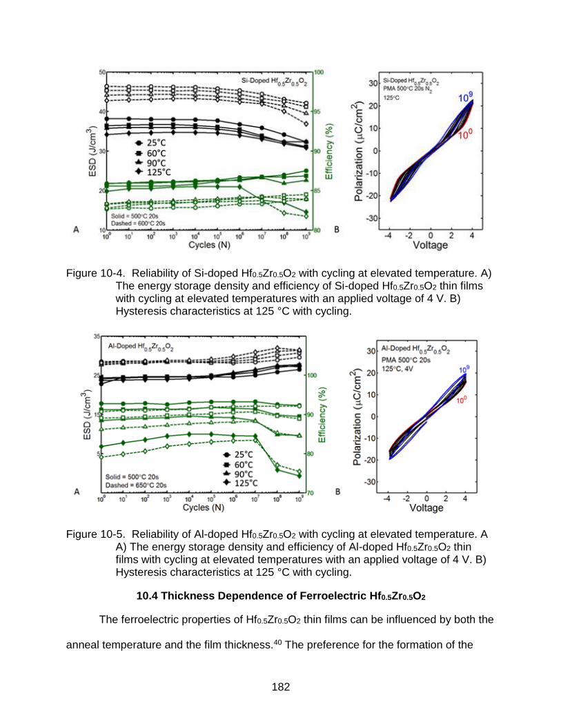
182
Figure 10-4. Reliability of Si-doped Hf0.5Zr0.5O2 with cycling at elevated temperature. A) The energy storage density and efficiency of Si-doped Hf0.5Zr0.5O2 thin films with cycling at elevated temperatures with an applied voltage of 4 V. B) Hysteresis characteristics at 125 °C with cycling.
Figure 10-5. Reliability of Al-doped Hf0.5Zr0.5O2 with cycling at elevated temperature. A A) The energy storage density and efficiency of Al-doped Hf0.5Zr0.5O2 thin films with cycling at elevated temperatures with an applied voltage of 4 V. B) Hysteresis characteristics at 125 °C with cycling.
10.4 Thickness Dependence of Ferroelectric Hf0.5Zr0.5O2
The ferroelectric properties of Hf0.5Zr0.5O2 thin films can be influenced by both the
anneal temperature and the film thickness.40 The preference for the formation of the

183
monoclinic, tetragonal, and orthorhombic crystal phases can vary with film thickness
where thicker films have a tendency to form the monoclinic phase.40,122 Thinner
Hf0.5Zr0.5O2 films (< 10 nm) tend to exhibit more severe pinching of the hysteresis loop
which suggests either a predominantly tetragonal film or a large depolarization field.151
Figure 10-6 shows the hysteresis loops of Hf0.5Zr0.5O2 thin films from 15 nm – 6 nm with
different anneal temperatures. All of the films show some degree of pinching of the P-E
loop in the as-fabricated state, although this diminishes as the anneal temperature
approaches 700 °C. The overall decrease in relative permittivity (taken from the slope of
the P-E loop) and the increase in the coercive field with anneal temperature is indicative
of an increase in the monoclinic phase, possibly grown on top of the o-phase or t-phase
as postulated by Park et al.40 Cycling the films results in opening up the hysteresis
loops, although the 6 nm Hf0.5Zr0.5O2 thin films remain slightly pinched.
Figure 10-6. Hysteresis characteristics of Hf0.5Zr0.5O2 thin films from 15 nm – 6 nm in thickness with different anneal temperatures. Cycling was carried out at 1kHz.

184
The much stronger pinching of the hysteresis loops in the 6 nm thick Hf0.5Zr0.5O2 films
corroborates the supposition of a depolarization field or a predisposition for the
formation of the tetragonal phase.151 The remanent polarization is largest in the 10 nm
thick Hf0.5Zr0.5O2 films and reach ~ 25 µC/cm2 after cycling. The 6 nm Hf0.5Zr0.5O2 films
have the smallest Pr due to their antiferroelectric-like characteristics. Cycling the films
results in a 5 – 10 µC/cm2 increase in the remanent polarization for all of the films which
may be attributable to a to phase conversion or depinning of ferroelectric
domains.77,82 The relative permittivity (Figure 10-8) is similar across film thicknesses,
and cycling leads to an overall reduction in εr. The high field shoulders in the εr-E plots
are similar to the double butterfly loops found in antiferroelectric films,75 but cycling
reduces these smaller peaks and the resultant curve takes the shape of a ferroelectric
butterfly loop. The 6 nm thick Hf0.5Zr0.5O2 films, however, have greater separation
between the high-field and low-field εr peaks and cycling does not completely lead to the
emergence of the classical ferroelectric butterfly loop.
Figure 10-7. The remanent polarization of the Hf0.5Zr0.5O2 films with thickness and anneal temperature, before and after cycling at 1 kHz.

185
Figure 10-8. The relative permittivity vs. electric field curves show that most of the films have secondary high-field shoulders which disappear after cycling, except in the case of the 6 nm thick Hf0.5Zr0.5O2 films. Cycling was carried out at 1 kHz and the Hf0.5Zr0.5O2 films in this figure were annealed at 500 °C.
Given the increase in the remanent polarization and the depinching of the
hysteresis loops with cycling, the retention characteristics of the Hf0.5Zr0.5O2 thin films
should be affected as well. Figure 10-9 shows the retention characteristics of 10 nm
thick Hf0.5Zr0.5O2 films from room temperature to 120 °C before and after cycling.
Cycling causes a significant increase in the polarization margin and an overall
improvement in the data retention compared to the as-fabricated films. The opposite
state retention for positive and negative states decreases the most after a 120 °C bake
which is indicative of imprint as being a reliability concern.
Figure 10-9. Retention characteristics of 10 nm Hf0.5Zr0.5O2 films before and after cycling at 1 kHz.

186
The thickness dependence of the retention characteristics was carried out on 15
nm, 10 nm, and 6 nm thick Hf0.5Zr0.5O2 films after cycling, Figure 10-10. Since the 6 nm
thick Hf0.5Zr0.5O2 films exhibited the most severe pinching of the P-E loop, the retention
characteristics may be unsuitable for nonvolatile memory applications. The data
retention was found to be the worst in the 6 nm thick Hf0.5Zr0.5O2 films, confirming strong
thickness dependence for the detrimental effect of a depolarization field or the
predominantly tetragonal film. The 15 nm thick Hf0.5Zr0.5O2 films did not have as large of
a polarization margin as the 10 nm thick films, possibly due to a smaller fraction of the
polar orthorhombic phase in the thicker film. Thus, the 10 nm thick films exhibit the best
retention characteristics of the Hf0.5Zr0.5O2 films.
Figure 10-10. Retention tests carried out on 15, 10, and 6 nm thick Hf0.5Zr0.5O2 films after cycling at 1 kHz.
The greater instability of the opposite state retention in the Hf0.5Zr0.5O2 thin films
is indicative of imprint. As shown in Figure 10-11, when Hf0.5Zr0.5O2 capacitors are
baked in a positive state, the hysteresis loops shift leftward and a negative state bake
leads to a shift to the right. Thus, the polarity of the internal electric field which forms
after baking the ferroelectric capacitors is dependent on the polarization state. Pinning
of ferroelectric domains due to charged defects such as oxygen vacancies or interfacial
trap states may be responsible for the observed imprint shifts with bakes.

187
Figure 10-11. Imprint shifts are shown in red and blue for positive and negative state bakes respectively.
10.5 Compositionally Graded HfxZr1-xO2 Thin Films
Pinching of the P-E loops in Hf0.5Zr0.5O2 thin films could pose a serious obstacle
for producing thin ferroelectric films for nonvolatile memory applications. To determine if
changing the composition of the films could be used to avoid such antiferroelectric-like
behavior, two different compositionally graded HfxZr1-xO2 thin films were fabricated. One
film is composed of a Hf0.5Zr0.5O2/Hf0.75Zr0.25O2/Hf0.5Zr0.5O2 stack structure which will be
referred to as the Hf-rich center (HRC) films. The other stack structure is composed of
Hf0.25Zr0.75O2/Hf0.75Zr0.25O2/Hf0.25Zr0.75O2 which will be referred to as the Zr-rich end
(ZRE) films. The hysteresis characteristics of the HRC films are shown in Figure 10-12.
As can be seen, virtually no pinching of the P-E loop occurs down to HRC films 6 nm
thick. At higher anneal temperatures than 600 °C, some distortion of the hysteresis
loops occur but it is attended by a decrease in the relative permittivity, indicating that the
growth of an interfacial layer or the separation of phases within the compositionally
graded films might be occurring. Cycling the HRC films results in a net increase in the
remanent polarization, but the Pr is lower than the binary Hf0.5Zr0.5O2 thin films. Since

188
the films have become more Hf-rich, it is very probable that the stability of the
monoclinic phase has been encouraged instead of tetragonal phase.39 The concomitant
disappearance of pinched hysteresis behavior and the reduced likelihood of the
formation of the tetragonal phase adds evidence that the tetragonal phase is indeed
responsible for the antiferroelectric-like behavior observed in binary Hf0.5Zr0.5O2 thin
films.
Figure 10-12. Hysteresis characteristics of Hf0.5Zr0.5O2 thin films with a Hf-rich center at different thicknesses and anneal temperatures. Cycling was performed at 1 kHz.
In contrast to the HRC films, the ZRE films show more pronounced pinched P-E
behavior for 10 nm and 6 nm thick films, as shown in Figure 10-13. Cycling is able to
open up the hysteresis loops, but they remain more or less antiferroelectric-like for the 6
nm thick films. Thus, the pinched P-E loop resulting from adding more Zr content to the

189
HfxZr1-xO2 can be attributed to increasing the tetragonal phase in 6 nm thick films which
accounts for the stronger antiferroelectric-like characteristics. The thicker 15 nm ZRE
films did not exhibit an antiferroelectric-like virgin hysteresis loop because the change in
surface energy and the Hf-rich central region likely made the tetragonal phase less
favorable.
Figure 10-13. Hysteresis characteristics of HfxZr1-xO2 thin films with a Hf-rich center and Zr-rich ends at different thicknesses and anneal temperatures. Cycling was performed at 1 kHz.
The retention of 6 nm thick HRC films were evaluated to determine if the lack of
antiferroelectric-like behavior in the as-fabricated capacitors would be associated with
an improvement in the retention properties. The HRC films were cycled at different
electric fields and underwent bakes up to 120 °C, as shown in Figure 10-14. While the
polarization margins are similar to binary Hf0.5Zr0.5O2 thin films at 3.5 MV/cm, higher

190
electric fields yield improvements in the data margins. The HRC films are notably more
stable at higher electric fields than binary Hf0.5Zr0.5O2 thin films with reduced leakage
currents and improved cycling endurance, therefore, higher electric field operation may
be feasible. While polarization margins in the 6 nm thick HRC films might be acceptable
up to 60 °C, higher temperatures lead to a deterioration in opposite state retention due
to an imprint shift caused by baking the capacitors in the positive or negative
polarization state.
Figure 10-14. The retention characteristics of the HRC films at 6 nm shows an increase
in the polarization margin with higher electric fields.
One possible explanation for the changes in ferroelectric behavior with
decreasing film thicknesses in the HfxZr1-xO2 thin films is the increasingly prominent role
an interfacial layer may play as the bulk ferroelectric region is reduced. In order to
determine the possible presence of an interfacial layer in ferroelectric thin films, a plot of
1/C vs film thickness can be used such that a linear extrapolation to zero film thickness
would uncover the interfacial capacitance at the y-intercept.108,153 Figure 10-15 shows
that extrapolating the inverse capacitance for the binary Hf0.5Zr0.5O2, HRC, and ZRE
films does in fact indicate that there may be an interfacial layer in at least two of the
films. Both the binary Hf0.5Zr0.5O2 and the ZRE films exhibit a positive intercept which is
evidence that these films have interfacial capacitance in series with the bulk ferroelectric

191
capacitance. Moreover, these two film types both exhibit pinched hysteresis
characteristics at 6 nm and the smaller interfacial capacitance term for the ZRE films in
comparison to the binary Hf0.5Zr0.5O2 films is correlated with stronger antiferroelectric-
like behavior.
Figure 10-15. Inverse capacitance with film thickness for binary Hf0.5Zr0.5O2, HRC, and ZRE films.
The slope of the linear lines in Figure 10-15 is the bulk ferroelectric capacitance and can
be used to extract the bulk relative permittivity of the different films. Using this method,
the bulk permittivity was found to be 45.6, 29.5, and 40.9 for the binary Hf0.5Zr0.5O2,
HRC, and ZRE films respectively. The significantly lower relative permittivity of the HRC
films indicate the presence of the monoclinic phase in the bulk. The inverse of the

192
(positive) intercepts can be used to extract the interface capacitance. Assuming the
interfacial layer is composed of the tetragonal phase (k ~ 70)13, the thickness of the
interfacial layer for the binary Hf0.5Zr0.5O2 would be less than an Å thick while the ZRE
films have an extracted interfacial layer thickness of 1.3 nm. The unrealistic interfacial
layer thickness for the binary Hf0.5Zr0.5O2 films is likely due to the greater uncertainty in
the linear extrapolation. However, a 1.3 nm interfacial layer in the ZRE films is plausible
due to the excellent linear fit to the measured data and the increased likelihood that the
tetragonal phase would be promoted in the Zr-rich end regions instead of the Hf-rich
bulk. In contrast to the binary Hf0.5Zr0.5O2 and the ZRE films, the HRC films exhibit a
negative intercept value which is incompatible with the presence of an interfacial layer.
The simultaneous absence of pinching and lack of an interfacial capacitance term in the
HRC films supports the hypothesis that an interfacial layer may be promoting pinching
of the hysteresis loops in ultrathin ferroelectric Hf0.5Zr0.5O2 thin films. Due to the
correlation between the preference for the tetragonal phase and the interfacial
capacitance term, it is likely that the tetragonal phase may predominantly form at the
electrode interfaces where it acts as both a parasitic capacitance layer and adds a field
dependent secondary switching current as a result of a to transition during nucleation
switching with the application of an electric field.
10.6 Conclusion
Hf0.5Zr0.5O2 thin films 10 nm thick were doped with Al or Si which produced
antiferroelectric behavior. The Si-doped Hf0.5Zr0.5O2 thin films exhibited a large 40 J/cm3
energy storage density with a 85% efficiency. The cycling characteristics of the Si-
doped Hf0.5Zr0.5O2 antiferroelectric thin were promising due to the robust performance
after undergoing 109 cycles up to 125 °C. The Al-doped Hf0.5Zr0.5O2 thin films were not

193
as robust due to the larger electric fields needed to generate a to field induced phase
transition.
Hf0.5Zr0.5O2 thin films of different thicknesses were fabricated and characterized.
Pronounced pinching of the P-E loops were observed in 6 nm thick Hf0.5Zr0.5O2 thin
films. Retention tests carried out on the films indicated the benefits of cycling compared
to as-fabricated ferroelectric Hf0.5Zr0.5O2 thin films. The retention characteristics were
best in the 10 nm thick Hf0.5Zr0.5O2 thin films and the 10 nm thick films also had the
largest remanent polarization. 6 nm thick Hf0.5Zr0.5O2 thin films exhibited very poor
retention characteristics in part due to the strongly pinched P-E loops seen in the as-
fabricated films.
Compositionally graded HfxZrx-O2 thin films showed that increasing the Hf content
within the center of the film could eliminate antiferroelectric-like behavior in the virgin
films down to 6 nm thick. In contrast, when the Zr content was increased in the graded
HfxZr1-xO2 thin films, antiferroelectric-like behavior became more pronounced in the 10
nm and 6 nm thick films. Films which favored a tetragonal structure as the thickness
was reduced, indicated by their antiferroelectric-like behavior, were also to found have
an interfacial capacitance term. It was postulated that the formation of the tetragonal
phase at the electrode interfaces could explain both the observation of a small signal
interfacial capacitance term and the antiferroelectric-like switching behavior where a
to phase transition occurs when large electric fields are applied to accomplish
nucleation and polarization reversal of existing ferroelectric domains.

194
CHAPTER 11 SUMMARY AND FUTURE WORK
Ferroelectric HfO2 thin films have the potential to be incorporated into nonvolatile
memory technologies such as FRAM and FeFETs. The ferroelectric characteristics of
nanometer-scale HfO2 films are highly dependent on a variety of factors including the
substrate, electrode interfaces, and the distribution of incorporated dopants as shown in
this dissertation. TiN and Ir electrodes were both found to promote ferroelectric behavior
in Si-doped HfO2 after post-metallization anneals. Chemical asymmetries in the
electrode/ferroelectric interfaces in Si-doped HfO2 thin films with sputtered TaN
electrodes led to imprint and the development of an internal electric field. When
ferroelectric HfO2 was grown on a Si substrate and annealed, the growth of an
interfacial SiO2 layer caused an increase in the switching voltage. Si-doped HfO2 thin
films grown on a Ge substrate did not have an observable interfacial layer and exhibited
a lower operating voltage compared to the Si MFIS device stack, highlighting the
potential for low-power Ge-based FeFETs in the MFS device structure.
Co-doping HfO2 with Al and Si produced ferroelectric behavior that was
dependent on how the dopants were layered. The remanent polarization was influenced
by the annealing conditions and the Al and Si dopant distribution. Si-layering in HfO2
thin films was also found to lead to alterations in the remanent polarization. Modifying
the ferroelectric characteristics of HfO2-based thin films through dopant layering is a
viable route to improve the performance of ferroelectric HfO2 for FRAM and FeFET
applications. Compositionally graded HfxZr1-xO2 thin films may enable tuning of the thin
film properties for specific applications while adding Al or Si dopants into HfxZr1-xO2 is
promising for energy storage capacitors and potentially infrared sensors. Moving

195
forward, a wide variety of fundamental scientific studies need to be conducted on the
ferroelectric HfO2 material system to better understand the mechanisms which stabilize
the polar orthorhombic phase. Future work on ferroelectric HfO2 can look at making the
films thinner than 5 nm for FTJ applications, implementing a Ge FeFET, and finding
ways to increase the robustness of the retention characteristics for other nonvolatile
memory technologies.

196
APPENDIX A PROCESS FLOW FOR FERROELECTRIC HfO2 CAPACITORS

197
APPENDIX B DESCRIPTION OF ATOMIC LAYER DEPOSITION PROCESS
Atomic layer deposition (ALD) is a thin film deposition technique whereby
individual atomic layers of a material are grown on a substrate. The growth of atomic
monolayers in ALD is a result of a self-limiting surface reaction as precursor molecules
adsorb onto the substrate. Once the substrate surface has been covered in adsorbed
precursor molecules, excess precursor molecules and byproducts are evacuated from
the ALD chamber. Next, a reactant such as a plasma or H2O is delivered to the
substrate surface which is blanketed with adsorbed precursor molecules. Once the ALD
precursor is exposed to a reactant, a surface reaction takes place in which a monolayer
of material has been grown on the substrate. After the precursor has been reacted, the
byproducts are then removed from the ALD chamber and another layer can be grown.
The process of growing one atomic layer is usually referred to as one ALD cycle.
By varying the number of ALD cycles and measuring the thickness of the grown layers,
it is possible to determine the growth rate of the precursor. Growth rates can be affected
by a variety of factors such as substrate temperature, surface chemistry, and choice of
reactant. The method of precursor reaction can divide ALD growth into two types,
thermal and plasma. Thermal ALD employs H2O as the reactant and is usually used in
growing oxides. Plasma ALD employs plasmas, such as O2, N2, and H2, to react with
the adsorbed precursor molecules. A combination of plasma and thermal ALD can be
used to great advantage in fabricating capacitors which require a high quality gate oxide
(thermal ALD of HfO2) and conducting electrodes (plasma ALD of TiN). ALD recipes can
be modified to grow structures in any sequence or combination of layers which makes it
a very flexible tool. The ability to tailor doping profiles and composition as a function of

198
position makes ALD the most suited deposition technique in which to explore
ferroelectric behavior in HfO2. Table B-1 lists the ALD precursors and the materials
grown from them in this dissertation. Figure B-1 shows the flow diagram of a basic ALD
program and Table B-2 lists the recipe specifications.
Table B-1. List of ALD precursors and the materials grown. ALD Precursors Chemical Formula Material Grown
Tetrakis(dimethylamido)hafnium [(CH3)2N]4Hf HfO2 Tris(dimethylamino)silane [(CH3)2N]3SiH SiO2 Trimethylaluminum Tetrakis(dimethylamido)titanium Tetrakis(dimethylamino)zirconium
(CH3)3Al [(CH3)2N]4Ti [(CH3)2N]4Zr
AlxOy
TiN ZrO2
Figure B-1. Flow diagram of an ALD recipe.

199
Table B-2. ALD recipe specifications. Material
Grown Substrate
Temperature Precursor
Pulse Precursor
Purge Reactant
Pulse Reactant
Purge Reactant
Type
HfO2 200°C .25s 15s .06s 15s H2O SiO2 200°C .4s 10s 20s 5s Plasma AlxOy 200°C .06s 20s .06s 10s H2O ZrO2 200°C .25s 20s .1s 10s H2O TiN 200°C .2s 6s 20s 5s Plasma
200
LIST OF REFERENCES
1 M. Dawber, K.M. Rabe, and J.F. Scott, Rev. Mod. Phys. 77, 1083 (2005).
2 C. Kittel, Introduction to Solid State Physics, Sixth (John Wiley & Sons, Inc., New York, 1986).
3 F.T. Ulaby, E. Michielssen, and U. Ravaioli, Fundamentals of Applied Electromagnetics, 6/E ed. (Prentive Hall, Upper Saddle River, 2010).
4 D. Damjanovic, Reports Prog. Phys. 61, 1267 (1998).
5 S. Hong, editor , Nanoscale Phenomena in Ferroelectric Thin Films (Kluwer Academic Publishers, Boston, 2004).
6 Y.L. Tang, Y.L. Zhu, Y.J. Wang, W.Y. Wang, Y.B. Xu, W.J. Ren, Z.D. Zhang, and X.L. Ma, Sci. Rep. 4, 4115 (2014).
7 E. Fatuzzo and W.J. Merz, Ferroelectricity (North-Holland Publishing Co., Amsterdam, 1967).
8 M. Kohli, P. Muralt, and N. Setter, Appl. Phys. Lett. 72, 3217 (1998).
9 H. Zhu, D.P. Chu, N.A. Fleck, S.E. Rowley, and S.S. Saxena, 105, 061609 (2010).
10 J. Rodel, A.B. Kounga, E. Aulbach, T. Granzow, and T. Leist, in Sixt. IEEE Int. Symp. Appl. Ferroelectr. (IEEE, Nara, 2007), pp. 638–640.
11 M.H. Lente and J.A. Eiras, J. Appl. Phys. 89, 5093 (2001).
12 J. Wang, H.P. Li, and R. Stevens, J. Mater. Sci. 27, 5397 (1992).
13 X. Zhao and D. Vanderbilt, Phys. Rev. B 65, 233106 (2002).
14 C.E. Curtis, L.M. Doney, and J.R. Johnson, J. Am. Ceram. Soc. 37, 458 (1954).
15 G.D. Wilk, R.M. Wallace, and J.M. Anthony, 89, 5243 (2001).
16 B.H. Lee, L. Kang, W. Qi, R. Nieh, Y. Jeon, K. Onishi, and J.C. Lee, in Int. Electron Devices Meet. (IEEE, Washington DC, 1999), pp. 133–136.
17 K. Tomida, K. Kita, and A. Toriumi, Appl. Phys. Lett. 89, 142902 (2006).
18 A. Toriumi, K. Kita, K. Tomida, and Y. Yamamoto, ECS Trans. 1, 185 (2006).
19 S. V Ushakov, C.E. Brown, and A. Navrotsky, Mater. Res. 19, 693 (2004).
20 T.S. Boscke, J. Muller, D. Brauhaus, U. Schroder, and U. Bottger, Appl. Phys. Lett. 99, 102903 (2011).

201
21 R. Ruh, H.J. Garrett, R.F. Domagala, and N.M. Tallan, J. Am. Ceram. Soc. 51, 23 (1968).
22 O. Ohtaka, H. Fukui, T. Kunisada, T. Fujisawa, K. Funakoshi, W. Utsumi, T. Irifune, K. Kuroda, and T. Kikegawa, J. Am. Ceram. Soc. 84, 1369 (2001).
23 J.E. Lowther, J.K. Dewhurst, J.M. Leger, and J. Haines, Phys. Rev. B 60, 485 (1999).
24 E.H. Kisi, J. Am. Ceram. Soc. 81, 741 (1998).
25 M.H. Park, Y.H. Lee, H.J. Kim, Y.J. Kim, T. Moon, K. Do Kim, J. Müller, A. Kersch, U. Schroeder, T. Mikolajick, and C.S. Hwang, Adv. Mater. 27, 1811 (2015).
26 E.P. Gusev, D.A. Buchanan, E. Cartier, A. Kumar, D. DiMaria, S. Guha, A. Callegari, S. Zafar, P.C. Jamison, D.A. Neumayer, M. Copel, M.A. Gribelyuk, H. Okorn-Schmidt, C. D’Emic, P. Kozlowski, K. Chan, N. Bojarczuk, L.-A. Ragnarsson, P. Ronsheim, K. Rim, R.J. Fleming, A. Mocuta, and A. Ajmera, in Int. Electron Devices Meet. (IEEE, Washington, DC, 2001), pp. 20.1.1–20.1.4.
27 B.H. Lee, L. Kang, R. Nieh, W.-J. Qi, and J.C. Lee, Appl. Phys. Lett. 76, 1926 (2000).
28 J.H. Choi, Y. Mao, and J.P. Chang, Mater. Sci. Eng. R Reports 72, 97 (2011).
29 R.D. Clark, Materials (Basel). 7, 2913 (2014).
30 T. Ando, Materials (Basel). 5, 478 (2012).
31 H. Kim, P.C. Mcintyre, C.O. Chui, K.C. Saraswat, and S. Stemmer, J. Appl. Phys. 96, 3467 (2004).
32 L.A. Ragnarsson, T. Chiarella, M. Togo, T. Schram, P. Absil, and T. Hoffmann, Microelectron. Eng. 88, 1317 (2011).
33 D. Fischer and A. Kersch, Microelectron. Eng. 84, 2039 (2007).
34 T. Roessler, J. Gluch, M. Albert, and J.W. Bartha, Thin Solid Films 518, 4680 (2010).
35 J. Müller, T.S. Böscke, U. Schröder, M. Reinicke, L. Oberbeck, D. Zhou, W. Weinreich, P. Kücher, M. Lemberger, and L. Frey, Microelectron. Eng. 86, 1818 (2009).
36 T.S. Boscke, P.Y. Hung, P.D. Kirsch, M.A. Quevedo-Lopez, and R. Ramirez-Bon, Appl. Phys. Lett. 95, 052904 (2009).
37 D.H. Triyoso, P.J. Tobin, B.E. White, R. Gregory, and X.D. Wang, Appl. Phys. Lett. 89, 132903 (2006).
38 J. Muller, T.S. Boscke, D. Brauhaus, U. Schroder, U. Bottger, J. Sundqvist, P. Kucher, T. Mikolajick, and L. Frey, Appl. Phys. Lett. 99, 112901 (2011).

202
39 J. Müller, T.S. Böscke, U. Schröder, S. Mueller, D. Bräuhaus, U. Böttger, L. Frey, and T. Mikolajick, Nano Lett. 12, 4318 (2012).
40 M. Hyuk Park, H. Joon Kim, Y. Jin Kim, W. Lee, T. Moon, and C.S. Hwang, Appl. Phys. Lett. 102, 242905 (2013).
41 S.E. Reyes-Lillo, K.F. Garrity, and K.M. Rabe, Phys. Rev. B 90, 140103 (2014).
42 R. Materlik, C. Künneth, and A. Kersch, J. Appl. Phys. 117, 134109 (2015).
43 H.J. Kim, M.H. Park, Y.J. Kim, Y.H. Lee, W. Jeon, T. Gwon, T. Moon, K.D. Kim, and C.S. Hwang, Appl. Phys. Lett. 105, 192903 (2014).
44 J. Muller, U. Schroder, T.S. Boscke, I. Muller, U. Bottger, L. Wilde, J. Sundqvist, M. Lemberger, P. Kucher, T. Mikolajick, and L. Frey, J. Appl. Phys. 110, 114113 (2011).
45 S. Mueller, J. Mueller, A. Singh, S. Riedel, J. Sundqvist, U. Schroeder, and T. Mikolajick, Adv. Funct. Mater. 22, 2412 (2012).
46 A. Chernikova, M. Kozodaev, A. Markeev, Y. Matveev, D. Negrov, and O. Orlov, Microelectron. Eng. 147, 15 (2015).
47 T. Olsen, U. Schroder, S. Muller, A. Krause, D. Martin, A. Singh, J. Muller, M. Geidel, and T. Mikolajick, Appl. Phys. Lett. 101, 082905 (2012).
48 S. Starschich, D. Griesche, T. Schneller, R. Waser, and U. Böttger, Appl. Phys. Lett. 104, 202903 (2014).
49 U. Schroeder, E. Yurchuk, J. Müller, D. Martin, T. Schenk, P. Polakowski, C. Adelmann, M.I. Popovici, S. V Kalinin, and T. Mikolajick, Jpn. J. Appl. Phys. 53, 08LE02 (2014).
50 T. Schenk, S. Mueller, U. Schroeder, R. Materlik, A. Kersch, M. Popovici, C. Adelmann, S. Van Elshocht, and T. Mikolajick, in 2013 Proc. Eur. Solid-State Device Res. Conf. (IEEE, Bucharest, 2013), pp. 260–263.
51 X. Sang, E.D. Grimley, T. Schenk, U. Schroeder, and J.M. LeBeau, Appl. Phys. Lett. 106, 162905 (2015).
52 J.A. Rodriguez, K. Remack, K. Boku, K.R. Udayakumar, S. Aggarwal, S.R. Summerfelt, F.G. Celii, S. Martin, L. Hall, K. Taylor, T. Moise, H. McAdams, J. McPherson, R. Bailey, G. Fox, and M. Depner, IEEE Trans. Device Mater. Reliab. 4, 436 (2004).
53 T. Eshita, W. Wang, K. Nakamura, S. Ozawa, Y. Okita, S. Mihara, Y. Hikosaka, H. Saito, J. Watanabe, K. Inoue, H. Yamaguchi, and K. Nomura, J. Phys. Sci. Appl. 5, 29 (2015).
203
54 J. Muller, P. Polakowski, S. Muller, and T. Mikolajick, ECS Trans. 64, 159 (2014).
55 P. Polakowski, S. Riedel, W. Weinreich, M. Rudolf, J. Sundqvist, K. Seidel, and J. Muller, in 2014 IEEE 6th Int. Mem. Work. (IEEE, Taipei, 2014), pp. 1–4.
56 N.A. Pertsev, J. Rodriguez Contreras, V.G. Kukhar, B. Hermanns, H. Kohlstedt, and R. Waser, Appl. Phys. Lett. 83, 3356 (2003).
57 Y. Sakashita, H. Segawa, K. Tominaga, and M. Okada, J. Appl. Phys. 73, 7857 (1993).
58 T. Sakoda, T.S. Moise, S.R. Summerfelt, L. Colombo, G. Xing, S.R. Gilbert, A.L.S. Loke, S. Ma, R. Kavari, L.A. Wills, and J. Amano, Jpn. J. Appl. Phys. 40, 2911 (2001).
59 M.H. Park, H.J. Kim, Y.J. Kim, W. Lee, H.K. Kim, and C.S. Hwang, Appl. Phys. Lett. 102, 112914 (2013).
60 J. Meena, S. Sze, U. Chand, and T.-Y. Tseng, Nanoscale Res. Lett. 9, 526 (2014).
61 T.S. Boscke, J. Muller, D. Brauhaus, U. Schroder, and U. Bottger, in 2011 Int. Electron Devices Meet. (IEEE, Washington, DC, 2011), pp. 24.5.1–24.5.4.
62 T.P. Ma and J.-P. Han, IEEE Electron Device Lett. 23, 386 (2002).
63 E. Yurchuk, J. Müller, J. Paul, T. Schlösser, D. Martin, R. Hoffmann, S. Müeller, S. Slesazeck, U. Schröeder, R. Boschke, R. van Bentum, and T. Mikolajick, IEEE Trans. Electron Devices 61, 3699 (2014).
64 E. Yurchuk, S. Mueller, D. Martin, S. Slesazeck, U. Schroeder, T. Mikolajick, J. Müller, J. Paul, R. Hoffmann, J. Sundqvist, T. Schlösser, R. Boschke, R. van Bentum, and M. Trentzsch, in 2014 IEEE Int. Reliab. Phys. Symp. (IEEE, Waikoloa, 2014), pp. 2E.5.1–2E.5.5.
65 T.P. Ma, in 2014 IEEE 6th Int. Mem. Work. (IEEE, Taipei, 2014), pp. 1–4.
66 C.-H. Cheng and A. Chin, IEEE Electron Device Lett. 35, 138 (2014).
67 C.H. Cheng and A. Chin, IEEE Electron Device Lett. 35, 274 (2014).
68 M.H. Lee, Y.-T. Wei, C. Liu, J.-J. Huang, M. Tang, Y.-L. Chueh, K.-Y. Chu, M.-J. Chen, H.-Y. Lee, Y.-S. Chen, L.-H. Lee, and M.-J. Tsai, IEEE J. Electron Devices Soc. 3, 377 (2015).
69 M.H. Park, H.J. Kim, Y.J. Kim, T. Moon, K.D. Kim, and C.S. Hwang, Adv. Energy Mater. 4, 1400610 (2014).
70 M.H. Park, H.J. Kim, Y.J. Kim, T. Moon, K.D. Kim, and C.S. Hwang, Nano Energy 12, 131 (2015).

204
71 M. Hoffmann, U. Schroeder, C. Künneth, A. Kersch, S. Starschich, U. Böttger, and T. Mikolajick, Nano Energy 18, 154 (2015).
72 C.B. Sawyer and C.H. Tower, Phys. Rev. 35, 269 (1930).
73 J.T. Evans, Introduction to the Ferroelectric Memory (Radiant Technologies Inc., Albuquerque, 2013).
74 T. Schenk, E. Yurchuk, S. Mueller, U. Schroeder, S. Starschich, U. Böttger, and T. Mikolajick, Appl. Phys. Rev. 1, 041103 (2014).
75 X. Hao, J. Zhai, L.B. Kong, and Z. Xu, Prog. Mater. Sci. 63, 1 (2014).
76 S. Bernacki, L. Jack, Y. Kisler, S. Collins, S.D. Bernstein, R. Hallock, B. Armstrong, J. Shaw, J. Evans, B. Tuttle, B. Hammetter, S. Rogers, B. Nasby, J. Henderson, J. Benedetto, R. Moore, C.R. Pugh, and A. Fennelly, Integr. Ferroelectr. 3, 97 (1993).
77 P.D. Lomenzo, Q. Takmeel, C. Zhou, C.M. Fancher, E. Lambers, N.G. Rudawski, J.L. Jones, S. Moghaddam, and T. Nishida, J. Appl. Phys. 117, 134105 (2015).
78 C.J. Brennan, Integr. Ferroelectr. 2, 73 (1992).
79 C.J. Brennan, MRS Proc. 243, 141 (1991).
80 L.M. Grupp, J.D. Davis, and S. Swanson, in Proc. 10th USENIX Conf. File Storage Technol. (USENIX Association, San Jose, CA, 2012).
81 S. Okamura, M. Takaoka, T. Nishida, and T. Shiosaki, Jpn. J. Appl. Phys. 39, 5481 (2000).
82 D. Zhou, J. Xu, Q. Li, Y. Guan, F. Cao, X. Dong, J. Muller, T. Schenk, and U. Schroder, Appl. Phys. Lett. 103, 192904 (2013).
83 M. Dawber and J.F. Scott, Appl. Phys. Lett. 76, 1060 (2000).
84 J.F. Scott, C.A. Araujo, B.M. Melnick, L.D. McMillan, and R. Zuleeg, J. Appl. Phys. 70, 382 (1991).
85 T. Hase, T. Noguchi, K. Takemura, and Y. Miyasaka, in Proc. Elev. IEEE Int. Symp. Appl. Ferroelectr. (IEEE, Montreux, 1998), pp. 7–10.
86 U. Robels and G. Arlt, J. Appl. Phys. 73, 3454 (1993).
87 A.K. Tagantsev, I. Stolichnov, E.L. Colla, and N. Setter, J. Appl. Phys. 90, 1387 (2001).
88 T. Schenk, U. Schroeder, M. Pešić, M. Popovici, Y. V Pershin, and T. Mikolajick, ACS Appl. Mater. Interfaces 6, 19744 (2014).

205
89 S. Mueller, J. Muller, U. Schroeder, and T. Mikolajick, IEEE Trans. Device Mater. Reliab. 13, 93 (2013).
90 U. Schroeder, S. Mueller, J. Mueller, E. Yurchuk, D. Martin, C. Adelmann, T. Schloesser, R. van Bentum, and T. Mikolajick, ECS J. Solid State Sci. Technol. 2, N69 (2013).
91 P.D. Lomenzo, Q. Takmeel, C. Zhou, C.-C. Chung, S. Moghaddam, J.L. Jones, and T. Nishida, Appl. Phys. Lett. 107, 242903 (2015).
92 M.H. Park, H.J. Kim, Y.J. Kim, W. Jeon, T. Moon, and C.S. Hwang, Phys. Status Solidi - Rapid Res. Lett. 8, 532 (2014).
93 D. Zhou, Y. Guan, M.M. Vopson, J. Xu, H. Liang, F. Cao, X. Dong, J. Mueller, T. Schenk, and U. Schroeder, Acta Mater. 99, 240 (2015).
94 R.R. Mehta, B.D. Silverman, and J.T. Jacobs, J. Appl. Phys. 44, 3379 (1973).
95 T.S. Boscke, S. Teichert, D. Brauhaus, J. Muller, U. Schroder, U. Bottger, and T. Mikolajick, Appl. Phys. Lett. 99, 112904 (2011).
96 N. Setter, D. Damjanovic, L. Eng, G. Fox, S. Gevorgian, S. Hong, A. Kingon, H. Kohlstedt, N.Y. Park, G.B. Stephenson, I. Stolitchnov, A.K. Taganstev, D. V. Taylor, T. Yamada, and S. Streiffer, J. Appl. Phys. 100, 051606 (2006).
97 E. Barsoukov and J.R. Macdonald, editors , Impedance Spectroscopy: Theory, Experiment, and Applications, 2nd ed. (John Wiley & Sons, Inc., Hoboken, NJ, 2005).
98 C. Verdier, F.D. Morrison, D.C. Lupascu, and J.F. Scott, J. Appl. Phys. 97, 024107 (2005).
99 L.-W. Chang, M. Alexe, J.F. Scott, and J.M. Gregg, Adv. Mater. 21, 4911 (2009).
100 N.J. Donnelly and C.A. Randall, IEEE Trans. Ultrason. Ferroelectr. Freq. Control 59, 1883 (2012).
101 A. Khodorov, S.A.S. Rodrigues, M. Pereira, and M.J.M. Gomes, J. Appl. Phys. 102, 114109 (2007).
102 F.D. Morrison, D.J. Jung, and J.F. Scott, J. Appl. Phys. 101, 094112 (2007).
103 C.R. Brundle, C.A.J. Evans, S. Wilson, and L.E. Fitzpatrick, editors , Encyclopedia of Materials Characterization (Manning Publicatins Co., Boston, MA, 1992).
104 K.R. Udayakumar, K. Boku, K.A. Remack, J. Rodriguez, S.R. Summerfelt, F.G. Celii, S. Aggarwal, J.S. Martin, L. Hall, L. Matz, B. Rathsack, H. McAdams, and T.S. Moise, Jpn. J. Appl. Phys. 45, 3202 (2006).
105 S. Mueller, S.R. Summerfelt, J. Müller, U. Schroeder, and T. Mikolajick, IEEE
206
Electron Device Lett. 33, 1300 (2012).
106 S. Mueller, C. Adelmann, A. Singh, S. Van Elshocht, U. Schroeder, and T. Mikolajick, ECS J. Solid State Sci. Technol. 1, N123 (2012).
107 K. Niwa, Y. Kotaka, M. Tomotani, H. Ashida, Y. Goto, and S. Otani, Acta Mater. 48, 4755 (2000).
108 R. Bouregba, N. Sama, C. Soyer, G. Poullain, and D. Remiens, J. Appl. Phys. 107, 104102 (2010).
109 H. Fujisawa, S. Hyodo, K. Jitsui, M. Shimizu, H. Niu, H. Okino, and T. Shiosaki, Integr. Ferroelectr. 21, 107 (1998).
110 H.O. Pierson, Handbook of Refractory Carbides & Nitrides: Properties, Characteristics, Processing and Applications (Noyes Publications, NJ, 1996).
111 J.W. Arblaster, Platin. Met. Rev. 33, 14 (1989).
112 A. Deshpande, R. Inman, G. Jursich, and C.G. Takoudis, J. Appl. Phys. 99, 094102 (2006).
113 J. Müller, E. Yurchuk, T.S. Böscke, R. Hoffmann, U. Schröder, T. Mikolajick, and L. Frey, in Proc. 17th Work. Dielectr. Microelectron. (2012), p. 1.
114 M.H. Park, H.J. Kim, Y.J. Kim, T. Moon, and C.S. Hwang, Appl. Phys. Lett. 104, 072901 (2014).
115 P.D. Lomenzo, P. Zhao, Q. Takmeel, S. Moghaddam, T. Nishida, M. Nelson, C.M. Fancher, E.D. Grimley, X. Sang, J.M. LeBeau, and J.L. Jones, J. Vac. Sci. Technol. B Microelectron. Nanom. Struct. 32, 03D123 (2014).
116 T.D. Huan, V. Sharma, G.A. Rossetti, and R. Ramprasad, Phys. Rev. B 90, 064111 (2014).
117 S. Mueller, E. Yurchuk, S. Slesazeck, T. Mikolajick, J. Muller, T. Herrmann, and A. Zaka, in 2013 Jt. IEEE Int. Symp. Appl. Ferroelectr. Work. Piezoresponse Force Microsc. (IEEE, Prague, 2013), pp. 248–251.
118 T. Rojac, M. Kosec, B. Budic, N. Setter, and D. Damjanovic, J. Appl. Phys. 108, 074107 (2010).
119 J. Muller, T.S. Boscke, U. Schroder, R. Hoffmann, T. Mikolajick, and L. Frey, IEEE Electron Device Lett. 33, 185 (2012).
120 S. Mueller, J. Müller, R. Hoffmann, E. Yurchuk, T. Schlösser, R. Boschke, J. Paul, M. Goldbach, T. Herrmann, A. Zaka, U. Schroder, and T. Mikolajick, IEEE Trans. Electron Devices 60, 4199 (2013).

207
121 T. Shimizu, T. Yokouchi, T. Shiraishi, T. Oikawa, P.S.S.R. Krishnan, and H. Funakubo, Jpn. J. Appl. Phys. 53, 09PA04 (2014).
122 E. Yurchuk, J. Müller, S. Knebel, J. Sundqvist, A.P. Graham, T. Melde, U. Schröder, and T. Mikolajick, Thin Solid Films 533, 88 (2013).
123 P.D. Lomenzo, Q. Takmeel, C. Zhou, Y. Liu, C.M. Fancher, J.L. Jones, S. Moghaddam, and T. Nishida, Appl. Phys. Lett. 105, 072906 (2014).
124 D. Martin, J. Müller, T. Schenk, T.M. Arruda, A. Kumar, E. Strelcov, E. Yurchuk, S. Müller, D. Pohl, U. Schröder, S. V. Kalinin, and T. Mikolajick, Adv. Mater. 26, 8198 (2014).
125 M.M. Hussain, N. Moumen, J. Barnett, J. Saulters, D. Baker, and Z. Zhang, Electrochem. Solid-State Lett. 8, G333 (2005).
126 L.A. Giannuzzi and F.A. Stevie, Micron 30, 197 (1999).
127 M. Sugiyama and G. Sigesato, J. Electron Microsc. (Tokyo). 53, 527 (2004).
128 L.A. Giannuzzi, J.L. Drown, S.R. Brown, R.B. Irwin, and F.A. Stevie, Microsc. Res. Tech. 41, 285 (1998).
129 J. Mayer, L.A. Giannuzzi, T. Kamino, and J. Michael, MRS Bull. 32, 400 (2007).
130 S. Bals, W. Tirry, R. Geurts, Z. Yang, and D. Schryvers, Microsc. Microanal. 13, 80 (2007).
131 N.I. Kato, J. Electron Microsc. (Tokyo). 53, 451 (2004).
132 N. Umezawa, K. Shiraishi, T. Ohno, H. Watanabe, T. Chikyow, K. Torii, K. Yamabe, K. Yamada, H. Kitajima, and T. Arikado, Appl. Phys. Lett. 86, 143507 (2005).
133 V. Cuny and N. Richard, J. Appl. Phys. 104, 033709 (2008).
134 A.K. Tagantsev, I. Stolichnov, N. Setter, J. Cross, and M. Tsukada, Phys. Rev. B 66, 214109 (2002).
135 B. Jaffe, Proc. IRE 49, 1264 (1961).
136 S.S.N. Bharadwaja and S.B. Krupanidhi, J. Appl. Phys. 89, 4541 (2001).
137 D. Martin, E. Yurchuk, S. Müller, J. Müller, J. Paul, J. Sundquist, S. Slesazeck, T. Schlösser, R. Van Bentum, M. Trentzsch, U. Schröder, and T. Mikolajick, Solid. State. Electron. 88, 65 (2013).
138 R. Pillarisetty, Nature 479, 324 (2011).
139 S.V.J. Chandra, M.-I. Jeong, Y.-C. Park, J.-W. Yoon, and C.-J. Choi, Mater. Trans.

208
52, 118 (2011).
140 H. Kim, C.O. Chui, K.C. Saraswat, and P.C. McIntyre, Appl. Phys. Lett. 83, 2647 (2003).
141 J. Müller, P. Polakowski, S. Riedel, S. Mueller, E. Yurchuk, and T. Mikolajick, in 2014 14th Annu. Non-Volatile Mem. Technol. Symp. (IEEE, Jeju Island, 2014), pp. 1–7.
142 S. Clima, D.J. Wouters, C. Adelmann, T. Schenk, U. Schroeder, M. Jurczak, and G. Pourtois, Appl. Phys. Lett. 104, 092906 (2014).
143 T. Schenk, M. Hoffmann, J. Ocker, M. Pešić, T. Mikolajick, and U. Schroeder, ACS Appl. Mater. Interfaces 7, 20224 (2015).
144 M. Hoffmann, U. Schroeder, T. Schenk, T. Shimizu, H. Funakubo, O. Sakata, D. Pohl, M. Drescher, C. Adelmann, R. Materlik, a. Kersch, and T. Mikolajick, J. Appl. Phys. 118, 072006 (2015).
145 P.D. Lomenzo, Q. Takmeel, C.M. Fancher, C. Zhou, N.G. Rudawski, S. Moghaddam, J.L. Jones, and T. Nishida, IEEE Electron Device Lett. 36, 766 (2015).
146 P. Polakowski and J. Müller, Appl. Phys. Lett. 106, 232905 (2015).
147 K.L. Lin, T.-H. Hou, J. Shieh, J.H. Lin, C.-T. Chou, and Y.-J. Lee, J. Appl. Phys. 109, 084104 (2011).
148 S.U. Sharath, T. Bertaud, J. Kurian, E. Hildebrandt, C. Walczyk, P. Calka, P. Zaumseil, M. Sowinska, D. Walczyk, A. Gloskovskii, T. Schroeder, and L. Alff, Appl. Phys. Lett. 104, 063502 (2014).
149 H.-Y. Chen and F.-H. Lu, J. Vac. Sci. Technol. A Vacuum, Surfaces, Film. 23, 1006 (2005).
150 H.C. Barshilia and K.S. Rajam, J. Mater. Res. 19, 3196 (2004).
151 M.H. Park, H.J. Kim, Y.J. Kim, Y.H. Lee, T. Moon, K.D. Kim, S.D. Hyun, and C.S. Hwang, Appl. Phys. Lett. 107, 192907 (2015).
152 H.J. Kim, M.H. Park, Y.J. Kim, Y.H. Lee, T. Moon, K.D. Kim, S.D. Hyun, and C.S. Hwang, Nanoscale 8, 1383 (2016).
153 P.K. Larsen, G.J.M. Dormans, D.J. Taylor, and P.J. van Veldhoven, J. Appl. Phys. 76, 2405 (1994).

209
BIOGRAPHICAL SKETCH
Patrick Lomenzo was born and raised in New Jersey. After living for a few years
in Morgantown, WV, Patrick moved to Florida and finished high school. Patrick earned
his Associate of Arts degree at Indian River State College and then transferred into the
Electrical and Computer Engineering Department at the University of Florida. While
working as an undergraduate researcher at UF, Patrick was approached with an
opportunity to work on an SRC project and was subsequently awarded an SRC
Fellowship to complete his PhD. He interned at Texas Instruments as a process
integration engineer for high voltage power technologies.


![openresearch.lsbu.ac.uk · Web view[] P. D. Thacher, Electrocaloric Effects in Some Ferroelectric and Antiferroelectric Pb(Zr, Ti)O 3 Compounds, J.Appl. Phys. 39 (1968), 1996-2002.](https://static.fdocuments.in/doc/165x107/5f0a51b07e708231d42b122a/web-view-p-d-thacher-electrocaloric-effects-in-some-ferroelectric-and-antiferroelectric.jpg)