Synthesis, Characterization and Ferroelectric Properties ...
62
University of South Florida Scholar Commons Graduate eses and Dissertations Graduate School 11-5-2015 Synthesis, Characterization and Ferroelectric Properties of LN-Type ZnSnO 3 Nanostructures Corisa Kons University of South Florida, [email protected] Follow this and additional works at: hp://scholarcommons.usf.edu/etd Part of the Materials Science and Engineering Commons , and the Physics Commons is esis is brought to you for free and open access by the Graduate School at Scholar Commons. It has been accepted for inclusion in Graduate eses and Dissertations by an authorized administrator of Scholar Commons. For more information, please contact [email protected]. Scholar Commons Citation Kons, Corisa, "Synthesis, Characterization and Ferroelectric Properties of LN-Type ZnSnO 3 Nanostructures" (2015). Graduate eses and Dissertations. hp://scholarcommons.usf.edu/etd/5976
Transcript of Synthesis, Characterization and Ferroelectric Properties ...

University of South FloridaScholar Commons
Graduate Theses and Dissertations Graduate School
11-5-2015
Synthesis, Characterization and FerroelectricProperties of LN-Type ZnSnO3 NanostructuresCorisa KonsUniversity of South Florida, [email protected]
Follow this and additional works at: http://scholarcommons.usf.edu/etd
Part of the Materials Science and Engineering Commons, and the Physics Commons
This Thesis is brought to you for free and open access by the Graduate School at Scholar Commons. It has been accepted for inclusion in GraduateTheses and Dissertations by an authorized administrator of Scholar Commons. For more information, please contact [email protected].
Scholar Commons CitationKons, Corisa, "Synthesis, Characterization and Ferroelectric Properties of LN-Type ZnSnO3 Nanostructures" (2015). Graduate Thesesand Dissertations.http://scholarcommons.usf.edu/etd/5976

Synthesis, Characterization and Ferroelectric Properties of LN-Type ZnSnO3
Nanostructures
by
Corisa Kons
A thesis submitted in partial fulfillment
of the requirements for the degree of
Master of Science
Department of Physics
College of Arts and Science
University of South Florida
Co- Major Professor: Anuja Datta, Ph.D.
Co- Major Professor: Pritish Mukherjee, Ph.D.
Manh-Huong Phan, Ph.D.
Date of Approval:
August 6, 2015
Keywords: nanowire, nanoparticle, nanoflake, hysteresis, solvothermal, pulsed-laser-deposition
Copyright © 2015, Corisa Kons

i
Table of Contents
List of Figures ................................................................................................................................ iii
Abstract ............................................................................................................................................v
Chapter 1: What are Ferroelectric Materials and Their Applications? ............................................1
1.1 Theory of Ferroelectrics .................................................................................................1
1.2 Pb-Free Nanostructured Ferroelectrics ..........................................................................5
1.2.1 LN-Type ZnSnO3 ............................................................................................6
1.3 Applications of Ferroelectric Materials .........................................................................8
1.4 References ......................................................................................................................9
Chapter 2: Experimental Methods and Characterization of LN-type ZnSnO3 Nanostructures .....12
2.1 Synthesis Equipment and Facilities .............................................................................12
2.1.1 Step I: Pulsed Laser Deposition (PLD) System for Thin Film Growth ........12
2.1.2 Step II: Chemical Synthesis of Nanostructures ............................................12
2.2 Characterization Equipment and Facilities ..................................................................13
2.2.1 Physics Materials Diagnostics Facility .........................................................13
2.2.2 Facility for Optical Characterization of Materials ........................................14
2.2.3 Other Resources and User Facilities Used In This Work at University of
South Florida ....................................................................................................15
2.3 General Synthesis and Characterization Overview ......................................................16
2.3.1 Deposition of Al-doped ZnO Template-Layer by PLD ................................16
2.3.2 Solvothermal Synthesis of LN-type ZnSnO3 Nanostructures .......................16
2.3.3 Fabrication of ZnSnO3 Nanostructure arrayed Ferroelectric Devices for
Polarization Measurements ..............................................................................17
2.4 Specific Experimental Parameters ...............................................................................18
2.4.1 Structural Growth of ZnSnO3 Nanowire Arrays by Physical/Chemical
Methods............................................................................................................18
2.4.2 Structural Growth of Hybrid ZnSnO3 Nanowire-Nanoparticle Arrays ........18
2.4.3 Structural Growth of Other ZnSnO3 Nanostructures ....................................19
Chapter 3: Ferroelectricity in LN-type ZnSnO3 Nanowire Arrays ................................................20
3.1 References ....................................................................................................................28
Chapter 4: Ferroelectricity in LN-type ZnSnO3 Nanowire-Nanoparticle Arrays ..........................30
4.1 References ....................................................................................................................40

ii
Chapter 5: Ferroelectricity in Pb-free LN-type ZnSnO3 Other Nanostructure Arrayed Thick
Films ........................................................................................................................................42
5.1 References ....................................................................................................................46
Chapter 6: Summary and Future Work ..........................................................................................47
6.1 References ....................................................................................................................48
Appendices .....................................................................................................................................49
Appendix 1: Publication List .............................................................................................49
1.1 Peer-Reviewed Journal Articles .......................................................................49
1.2 Peer-Reviewed Conference Proceedings .........................................................49
1.3 Conference Presentations .................................................................................49
Appendix 2: Copyright Permissions ..................................................................................51

iii
List of Figures
Figure 1.1 A broad overview of the 32 crystal classes, or point groups, showing a break-
down of each category leading to possible ferroelectric materials ............................................2
Figure 1.2 A typical electric polarization-electric field hysteresis plot of ferroelectricity ..............3
Figure 1.3 A graph depicting the relationship between spontaneous polarization and
temperature ................................................................................................................................4
Figure 1.4 Projection of ZnSnO3 crystal structure on (a) (110), (b) (101), and (c) (011)
planes .........................................................................................................................................7
Figure 1.5 Schematic diagram of the various applications of ferroelectric materials .....................8
Figure 2.1 Equipment used for substrate preparation and synthesis ..............................................13
Figure 2.2 Equipment used for characterization of ZnSnO3 arrayed films....................................14
Figure 2.3 A picture of the ferroelectric probe for detailed analysis of the ferroelectric
behavior of the ZnSnO3 nanostructured samples .....................................................................15
Figure 3.1 Overview of structural growth and fabricated device ..................................................21
Figure 3.2 SEM images taken at various stages of synthesis ........................................................22
Figure 3.3 Structural characterization of ZnSnO3 nanowire arrayed film .....................................23
Figure 3.4 (a) A top-down SEM image of the dense, non-porous ZnSnO3 nanowire fused
over-layer covering the substrate and hiding the nanowire arrays beneath .............................24
Figure 3.5 Results of ferroelectric behavior in the nanowire arrayed film ....................................26
Figure 4.1 (a) XRD of the as-prepared LN-type ZnSnO3 nanowire-nanoparticle arrayed |
film confirming phase purity as compared to Inaguma et al ...................................................31
Figure 4.2 (a and b) SEM images showing the densely packed, vertically aligned ZnSnO3
nanowires with attached nanoparticles ....................................................................................32
Figure 4.3 Fabricated sample alongside the corresponding hysteresis loop ..................................34

iv
Figure 4.4 Structural characterization and various hysteresis loops ..............................................35
Figure 4.5 Interaction of nanoparticle dipoles with nanowires and the resulting hysteresis .........37
Figure 4.6 Results of sample with improved nanoparticle concentration ......................................39
Figure 5.1 Structural results of various ZnSnO3 nanostructures....................................................43
Figure 5.2 Ferroelectric hysteresis loops of various ZnSnO3 nanostructures ................................45

v
Abstract
With increasing focus on the ill health and environmental effects of lead there is a greater
push to develop Pb-free devices and materials. To this extent, ecofriendly and earth abundant
LiNbO3-type ZnSnO3, a derivative of the ABO3 perovskite structure, has a high theoretically
predicted polarization making it an excellent choice as a suitable alternative to lead based
material such as PZT. In this work we present a novel synthesis procedure for the growth of
various ZnSnO3 nanostructures by combined physical/chemical processes. Various ZnSnO3
nanostructures of different dimensions were grown from a ZnO:Al template layer on a Si (100)
substrate deposited by pulsed laser deposition followed by a strategic solvothermal process. The
ferroelectric properties of each sample were explored and a remanent polarization as high as
nearly 30 µC/cm2 was found in aligned nanowire arrayed films. An in-depth understanding of the
structure-property relationship is key to the future development of this material and is the subject
of future investigations.

1
Chapter 1:
What are Ferroelectric Materials and Their Applications?
1.1 Theory of Ferroelectrics
Ferroelectricity is a property unique to materials that exhibit a reversible spontaneous
electric polarization in the presence of an applied external electric field, it is a cooperative
phenomenon that arises from the lattice of the polar material. In ABO3 perovskite oxides and
derivatives of such structures the spontaneous polarization is due a small displacement between
the cation and oxygen ion. The ability for ferroelectricity is limited to select crystal groups; of
the thirty-two point groups only twenty-one are non-centrosymmetric (NCS), or without a center
of symmetry, a trait necessary for ferroelectricity. The lack of an inversion point in NCS crystals
is essential for charge separation leading to polarization, an occurrence necessary for the
piezoelectric (PE) effect experienced by twenty of the NCS point groups. In the cubic point
group 432 symmetry arguments restrict the ability of a crystal to induce a dipole moment and so
cannot be PE.[1] Half the PE point groups feature a unique polar axis leading to spontaneous
polarization, for all materials of this nature a pyroelectric effect is also observed due to the
temperature dependence of the intrinsic polarization.[2,3]
All ferroelectric (FE) materials are a subset of the pyroelectric point groups, as shown in
Figure 1.1, but while all FEs are pyroelectrics the converse is not true. For a pyroelectric material
to be considered FE it must satisfy the Anderson and Blount conditions for ferroelectricity; there
must be a continuous phase transition from a centrosymmetric structure to one without inversion
symmetry and have a unique polar axis.[4] The change from a paraelectric centrosymmetric

2
structure to a polarized NCS one is necessary for spontaneous polarization since it is a result of
symmetry breaking due to the structural transition.[5]
Figure 1.1 A broad overview of the 32 crystal classes, or point groups, showing a breakdown of each
category leading to possible ferroelectric materials.
In all FE materials there is an accompanying non-linear behavior relating polarization and
electric field, a typical P-E hysteresis curve is shown in Figure 1.2 Electric polarization is a
measure of the average dipole moment volume density; it is an indicator of how strong and well-
aligned the dipoles are in a material. When an electric field is applied to a FE material the
polarization rapidly increases before becoming linear, it is at this point that extrapolation to the
zero electric field determines the value of spontaneous polarization (PS).[6] The electric field that
returns the polarization to zero from its maximum value is known as the coercive field (EC).
When the electric field is reduced to zero the remanent polarization (Pr) is what remains of the
spontaneous polarization.[7] The maximum value Pr can attain is that of the spontaneous
polarization (PS), it is a marker of the permanent dipole moment. Squareness of a hysteresis loop
is defined as the ratio of remanent polarization to spontaneous polarization (Pr/PS); a higher

3
squareness value is sought for FE materials as it means the remanent polarization is approaching
the theoretical maximum. Anomalous FE behavior can lead to asymmetry or constriction in P-E
hysteresis loops as a result of defect dipoles or other charge effects that cause deviation from
typical hysteresis loop behavior.
Figure 1.2 A typical electric polarization-electric field hysteresis plot of ferroelectricity. The spontaneous
polarization (PS) is determined by the line extrapolated at high electric field to the zero field. The electric
field that brings polarization to zero is known as the coercive field (EC). Remanent polarization (Pr) is the
remaining polarization present in the material in the absence of an applied electric field.
The pyroelectric effect is seen in FE materials in the form of temperature dependence of
spontaneous polarization. An increase in temperature is accompanied by a reduction in
spontaneous polarization due to the rising thermal energy that disorients the dipoles. The height
and width of the hysteresis curve shrink until the temperature surpasses the transition
temperature, or FE Curie temperature (TC), at which a phase transition occurs and the material
becomes paraelectric, meaning no spontaneous polarization; for this reason, spontaneous
polarization is greatest at temperature well below TC, as shown in Figure 1.3 below.[8] Above

4
the phase transition temperature there are no symmetry breaking distortions so the material can
only be centrosymmetric, meaning charge separation cannot occur.
Figure 1.3 A graph depicting the relationship between spontaneous polarization and temperature. Above
Tc the material becomes paraelectric and has no spontaneous polarization.
Since polarization is a vector, there is a direction associated with its magnitude, groups of
similarly oriented dipoles are known as a domain.[8] Domain walls are the boundaries between
different dipoles, groups of dipoles aligned in varying directions; much like a fence separates
yards.[6] The application of an external electric field will change the direction of the polarization
within a domain; the dipoles will want to align with the applied electric field, leading to a
process known as domain switching.[7] In some cases the presence of an internal bias field due
to defect dipoles can affect the field necessary for domain switching resulting in anomalous
behavior of the hysteresis loop. The alignment of dipoles at changing electric field will vary
spontaneous polarization, meaning the hysteresis curve is a measure of the work required to
move domain walls and the energy barrier that separates the different polarization directions.[9]

5
1.2 Pb-Free Nanostructured Ferroelectrics
Nanotechnology is already in use for next-generation computing, communications, and
other electronic applications to provide faster, smaller, energy-efficient systems that can manage,
and store information (memory).[10-15] In addition to enhancing the performance of functional
nanoscale-devices, a major concern for scientists is also to develop preparative processes and
materials towards cleaner environment and affordable technology. [16-21] The family of lead-
based perovskites such as Pb(Zr,Ti)O3 (PZT) has been extensively pursued as viable ferro- and
piezo-materials owing to its’ high-polarization (coercive field of about 1 kV/mm and a Pr of
about 35 µC/cm2 in bulk). [10-13],[22,23] Despite the efficacy of PZT, the widespread concern
on using toxic Pb in memory devices have resulted in efforts to find high-efficiency
environment-friendly materials.[16-21]
In this direction, an increased interest has developed around the polar NCS oxide
materials, which possess multi-functionality with high dielectric and PE coefficients, switchable
FE polarization, non-linear optical and electrical properties, and high mechanical stability.
[24,25] These properties identify them as next-generation ‘smart materials’, which are of high
academic and commercial interest. NCS oxides containing main-group cations with the
electronic configuration of (n-1)d10ns0, such as ZnO and have been widely studied to possess
enhanced symmetry dependent properties.[11,16,17] LiNbO3 (LN)-type compounds, which can
be described as a derivative of the perovskite-type structure (ABO3) as shown in Figure 1.4a,[24]
because both LN-type and perovskite-type compounds possess three-dimensionally corner-
sharing BO6 octahedra. The cooperative cation shift along the c-axis direction against close-
packed anions, results in spontaneous polarization in these types of oxide compounds. In such
compounds, ferroelectricity may be the result of B-site distortions, or more rarely, A-site.

6
1.2.1 LN-Type ZnSnO3: The growing concern of the health and environmental impact of
lead (Pb) in electronics and FE materials [26,27] has spurred much research in developing Pb-
free FE materials.[28-30] To this end, perovskite oxides of ABO3 phase offer a plethora of
possibilities due to the versatility of the structure in which the A and B sites can accommodate
nearly any element resulting in an impressive range of properties that can be adjusted based on
suitable A and B element choices.[31] Composed of earth abundant elements LN-type ZnSnO3 of
space group R3c (No. 161) has been reported to have a theoretical maximum polarization of ≈ 59
μC/cm2, [32] while experimental reports of epitaxial (111) ZnSnO3 thin films feature a high
remanent polarization of ~ 47 μC/cm2 at a coercive field of ~ 130 kV/cm and a maximum
polarization of 58μC/cm2.[33] Lattice parameters have also been theoretically calculated for LN-
type ZnSnO3; a = 5. 3441 Å and c = 14.2206 Å.[34]
In this work, ZnSnO3 adopts the LiNbO3 hexagonal structure with rhombohedral
symmetry, as seen in Figure 1.4. Containing no ferroelectrically-active cations (d0) or lone-pair
cations, and a tolerance factor less than 1 it is surprising that zinc stannate exhibits
ferroelectricity at all but unlike most perovskite oxides the reason for its intrinsic polarization is
tied to the displacement of the A site cation.[24] In the hexagonal structure the layers follow a
Zn-Sn-Vacancy-Zn-Sn-Vacancy-… pattern, as can be seen in Figure 1.4b-c, and the Zn ion is
distorted along the c-axis toward the vacant site possibly due to an electrostatic field within the
lattice tied to the strong ionic character of the cation.[35] This distortion leads to different two
different Zn-O bond lengths so Zn bonds differently to three O compared to the other three O
and this variation allows for spontaneous polarization in the c-direction.[32] The smaller radius
of the Zn cation (1.31 Å) compared to the Sn atom (1.41 Å) allows for more displacement of the
Zn in the vacancies.[33]

7
Figure 1.4 Projection of ZnSnO3 crystal structure on (a) (110), (b) (101), and (c) (011) planes. Reprinted
from [34] with permission from Elsevier.
Inaguma et al. reported that ZnSnO3 with a hexagonal LiNbO3(LN)-type structures
synthesized under high pressure, possess high-polarization (exhibiting long range alignment of
electric dipoles).[32,36] Reports on functional LN-type oxides relative to perovskite-type oxides
have been limited due to the difficulty in synthesizing these metastable phases by traditional
solid state synthesis processes under ambient conditions. In case of ZnSnO3, this may be due to
the ease of disproportionation of Zn2+ to Zn4+ and Zn metal to form hexagonal symmetry lattice.
An enhanced covalence qualifies the electronic structure as it can be inferred from analyzing the
chemical bonding. This lead us to search for a novel, and less conventional, non-equilibrium
bottom-up synthesis scheme such as combination of pulsed laser deposition (PLD) and
solvothermal in synthesizing these phases. As an advanced tool for growing high-quality
complex oxide thin films, PLD has made a significant impact in terms of growth of single- and
multi-layered heterostructures of multi-component materials.[32,36,37] When combined with

8
inexpensive, scalable chemical synthesis techniques, PLD can qualify to be an easy and rapid
way to design nanostructures of many important FE materials of high quality and high efficiency
and is the main focus of this thesis. We are the first to synthesize LN-type ZnSnO3 nanowire
arrays on silicon (Si) substrates using a novel physical-chemical approach encompassing pulsed
laser deposition (PLD) deposited ZnO:Al seed-layer and conventional hydrothermal processes
(to be discussed in later chapters).[37,38]
1.3 Applications of Ferroelectric Materials
Figure 1.5: Schematic diagram of the various applications of ferroelectric materials. Reproduced from
[15] with permission of The Royal Society of Chemistry.
The polarization of FE materials can be changed by using three forms of energy, i.e.
electric, thermal and mechanical or vice versa. These three inter-dependent properties of FEs
have been widely exploited for many functional applications.[15,39] The various applications of
FEs are schematically shown in Figure 1.5. The reversible polarization of a FE material can be

9
used in nonvolatile memory applications, as the direction of polarization switching represents the
binary ‘1’ and ‘0’ in data storage. [15,39] The FE thin films have already shown potential as
FeRAMs in memory storage applications. [15,39] The piezo effect in FEs can be used to convert
mechanical energy to electrical energy, or vice versa, and find wide-spread use as actuators,
transducers and micro-electromechanical (MEMS) devices. [15,39] As all FE materials are
pyroelectric, they can also generate an electrical current in response to any change in ambient
temperature; this principle, finds use in infrared thermal imaging.[15]
Significant efforts have been made recently to achieve high efficiency FE memory
devices, through the assistance of nanostructuring.[15,39,40] Different types of nanodevice
architectures with improved features have been realized, based on the reversible polarization of
the FEs. By scaling down the size of individual memory cells, the storage efficiency of FeRAMs
can be greatly improved. PE nanostructures, especially nanowires, have been studied extensively
for their potential energy harvesting capabilities from collective mechanical movements.
[15,39,40] Electrical energy collected from PE nanostructures has already been used effectively
to power nanoelectronics devices and sensors. One dimensional nanostructures, especially
nanowires and rods, have mostly been used for piezotronics applications due to their large
mechanical strain tolerance, especially the vertically or horizontally aligned arrays of PE
nanowires.
1.4 References
[1] M.M. Julian, Foundations of crystallography with computer applications, CRC Press,
Boca Raton, 2008, p. 135.
[2] W.-D. Cheng, C.-S. Lin, L. Geng, Z.-Z. Luo, W.-L. Zhang, H. Zhang, Syntheses and
Properties of Some Bi-Containing Compounds with Noncentrosymmetric Structure in H.
Li, Z.M. Wang (Eds.), Bismuth-containing compounds. Springer, New York, 2013, p.
323
[3] B. Jiménez, J.A. Gonzalo, Ferroelectricity, Wiley-VCH Verlag GmbH, 2007, p. 1.
[4] P.W. Anderson, E.I. Blount, Phys Rev Lett 14 (1965) 217.

10
[5] V. Keppens, Nat Mater 12 (2013) 952.
[6] S.L. Kakani, A. Kakani, Material science, New Age International (P) Ltd., Publishers,
New Delhi, 2004.
[7] G. Ravichandran, in: W.N. Sharpe, Jr. (Ed.), Springer Handbook of Experimental Solid
Mechanics, Springer US, 2008, p. 159.
[8] P. Maheshwari, Electronic components and processes. [electronic resource], New Delhi :
New Age International, c2006., 2006.
[9] S.C. Abrahams, K. Nassau, in: R.J. Brook (Ed.), Concise Encyclopedia of Advanced
Ceramic Materials, Pergamon, Oxford, 1991, p. 152.
[10] J.F. Scott, Ferroelectric memories, Springer, Berlin ; New York, 2000.
[11] A.J. Moulson, J.M. Herbert, Electroceramics: Materials, Properties, Applications, Wiley,
2003.
[12] S. Xu, B.J. Hansen, Z.L. Wang, Nat Commun 1 (2010) 93.
[13] K. Lubitz, C. Schuh, T. Steinkopff, A. Wolf, in: N. Setter (Ed.), Piezoelectric Materials
and Devices, Lausanne, 2002.
[14] H. Han, Y. Kim, M. Alexe, D. Hesse, W. Lee, Advanced Materials 23 (2011) 4599.
[15] J. Varghese, R.W. Whatmore, J.D. Holmes, J Mater Chem C 1 (2013) 2618.
[16] P. Hiralal, H.E. Unalan, G.A.J. Amaratunga, Nanotechnology 23 (2012).
[17] Z.L. Wang, J.H. Song, Science 312 (2006) 242.
[18] A. Navrotsky, Chemistry of Materials 10 (1998) 2787.
[19] J.M. Wu, C. Xu, Y. Zhang, Y. Yang, Y.S. Zhou, Z.L. Wang, Advanced Materials 24
(2012) 6094.
[20] J.M. Wu, C.Y. Chen, Y. Zhang, K.H. Chen, Y. Yang, Y.F. Hu, J.H. He, Z.L. Wang, Acs
Nano 6 (2012) 4369.
[21] J.M. Wu, C. Xu, Y. Zhang, Z.L. Wang, Acs Nano 6 (2012) 4335.
[22] N. Izyumskaya, Y. Alivov, S.J. Cho, H. Morkoc, H. Lee, Y.S. Kang, Crit Rev Solid State
32 (2007) 111.
[23] J. Kim, S.A. Yang, Y.C. Choi, J.K. Han, K.O. Jeong, Y.J. Yun, D.J. Kim, S.M. Yang, D.
Yoon, H. Cheong, K.-S. Chang, T.W. Noh, S.D. Bu, Nano Lett 8 (2008) 1813.
[24] N.A. Benedek, C.J. Fennie, J Phys Chem C 117 (2013) 13339.
[25] P.S. Halasyamani, K.R. Poeppelmeier, Chemistry of Materials 10 (1998) 2753.
[26] H. Black, Environmental Health Perspectives 113 (2005) A682.
[27] J. Pareja-Carrera, R. Mateo, J. Rodríguez-Estival, Ecotoxicology and Environmental
Safety 108 (2014) 210.
[28] I.P. Raevski, S.A. Prosandeev, Journal of Physics and Chemistry of Solids 63 (2002)
1939.
[29] N.K. Noel, S.D. Stranks, A. Abate, C. Wehrenfennig, S. Guarnera, A.-A. Haghighirad, A.
Sadhanala, G.E. Eperon, S.K. Pathak, M.B. Johnston, A. Petrozza, L.M. Herz, H.J.
Snaith, Energy & Environmental Science 7 (2014) 3061.
[30] J. Rödel, K.G. Webber, R. Dittmer, W. Jo, M. Kimura, D. Damjanovic, Journal of the
European Ceramic Society 35 (2015) 1659.
[31] D.G. Schlom, L.-Q. Chen, X. Pan, A. Schmehl, M.A. Zurbuchen, Journal of the
American Ceramic Society 91 (2008) 2429.
[32] Y. Inaguma, M. Yoshida, T. Katsumata, J Am Chem Soc 130 (2008) 6704.
[33] J.Y. Son, G. Lee, M.H. Jo, H. Kim, H.M. Jang, Y.H. Shin, J Am Chem Soc 131 (2009)
8386.

11
[34] H. Wang, H. Huang, B. Wang, Solid State Communications 149 (2009) 1849.
[35] M. Nakayama, M. Nogami, M. Yoshida, T. Katsumata, Y. Inaguma, Advanced Materials
22 (2010) 2579.
[36] Y. Inaguma, D. Sakurai, A. Aimi, M. Yoshida, T. Katsumata, D. Mori, J. Yeon, P.S.
Halasyamani, Journal of Solid State Chemistry 195 (2012) 115.
[37] A. Datta, D. Mukherjee, C. Kons, S. Witanachchi, P. Mukherjee, Small 10 (2014) 4093.
[38] D. Mukherjee, A. Datta, C. Kons, M. Hordagoda, S. Witanachchi, P. Mukherjee, Applied
Physics Letters 105 (2014).
[39] J. Rodel, W. Jo, K.T.P. Seifert, E.M. Anton, T. Granzow, D. Damjanovic, Journal of the
American Ceramic Society 92 (2009) 1153.
[40] S. Hong, Nanoscale phenomena in ferroelectric thin films, Kluwer Academic Publishers,
Boston, 2004.

12
Chapter 2:
Experimental Methods and Characterization Techniques of LN-type ZnSnO3 Nanostructures
2.1 Synthesis Equipment and Facilities
2.1.1 Step I: Pulsed Laser Deposition (PLD) System for Thin Film Growth: The state-of-
the-art PLD systems located in the Laboratory for Advanced Materials Science and Technology
(LAMSAT), Interdisciplinary Sciences (ISA) building, Department of Physics, USF, was used
for the deposition of seed-layers on hard conducting substrates. The various custom-built PLD
systems available consist of vacuum deposition chambers with pulsed lasers such as 248 nm KrF
excimer, 1064 nm (532 nm) Nd:YAG, and 10.6 µm CO2 lasers. The vacuum systems are capable
of sub-microtorr background pressures which can be back filled with inert or reactive gasses, as
required. A multi-target changer is available allowing in-situ deposition of multi-layers with
clean interfaces. An intensified charge-coupled detector (ICCD) imaging system aligned
perpendicular to the plume propagation enables two-dimensional imaging and spectroscopic
analysis of the laser-induced plume, allowing in-situ monitoring of the process. An illustration of
the PLD setup can be seen in Figure 2.1a.
2.1.2 Step II: Chemical Synthesis of Nanostructures: The established chemical synthesis
facilities used in this work include: fumehood for handling chemicals, Fisherprice Magnetic
heater and stirrers for preparing homogenized precursor solutions, SRC Ultrasonic cleaners for
cleaning substrates, Yamato gravity convection oven with controlled PID controller operational
up-to 300 ˚C for solvothermal reaction of the precursors in presence of the seed-layers,
Panasonic Commercial microwave oven for easy and rapid reaction of the seed-layers thin-films,

13
digestion reactors for solvothermal synthesis both for convection oven (parr instruments),
Champion variable speed centrifuge for cleaning reactants, vacuum drying oven for drying
samples (custom-made). Pictures of the autoclave and reaction chamber can be seen in Figure
2.1b.
Figure 2.1 (a) A schematic of the PLD setup used for deposition of ZnO:Al on Si (100) substrate. (b)
Equipment used for solvothermal synthesis.
2.2 Characterization Facilities and Equipment
2.2.1 Physics Materials Diagnostics Facility: User Facilities available at the Department
of Physics, University of South Florida, were extensively used to obtain results discussed in this
thesis. The Physics Materials Diagnostics Facility equipment used include an X-ray
diffractometer, Scanning Electron Microscope, and Energy Dispersive X-ray Spectroscopy. X-
Ray Diffractometer (Figure 2.2a) for characterization including crystal orientation, phase
identification, quantitative phase analysis, crystallite size, and lattice dimensions. The X-ray
Diffractometer (XRD) is a Bruker-AXS D8 Focus powder diffractometer with a Cu anode (Kα1
λ=1.5406Å), Bragg-Brentano geometry configuration, fixed divergence slits (0.1 to 6mm), high-
speed detector, and intuitive operation. The XRD is used for non-destructive characterization of
(a) (b)

14
materials in the form of powders, thin-films, single crystals, and bulk. The Scanning Electron
Microscope (SEM), shown in Figure 2.2b, is a JEOL JSM-6390LV with tungsten filament, low-
vacuum mode option, and intuitive operation. The SEM scans the sample with a focused beam of
electrons to characterize the surface morphology of the samples at a magnification range of 5x to
300,000x, producing high-resolution photo-quality images. Intricate morphological details are
obtained through this technique. The Energy Dispersive X-ray Spectroscopy (EDS) system is an
Oxford Instruments; INCAx-sight 7582M, liquid-nitrogen cooled EDS. The EDS system is
integrated with the JEOL JSM-6390LV SEM. The EDS (shown in Figure 2.2b) is an analytical
technique used for qualitative or quantitative elemental analysis or chemical characterization of
materials capable of detecting concentrations as low as 1% with ±0.1% accuracy. The high-
energy beam of electrons, provided by the SEM, stimulates the emission of characteristic X-rays
that allows the composition of the sample to be determined.
Figure 2.2 (a) The X-ray diffractometer used for structural characterization alongside (b) the Scanning
electron Microscope and Energy-dispersive X-ray spectroscope used for structural characterization as
well. (c) The Raman equipment used for optical studies.
2.2.2 Facility for Optical Characterization of Materials: The Raman spectroscopy system
(shown in Figure 2.2c) is a Horiba Jobin Yvon T64000 Advanced Research Raman System with
a Synapse charge-coupled device (CCD) detection system, and a confocal LabRAM Raman
microprobe. It has an integrated triple spectrometer design for unprecedented optical stability.
(c) (b) (a)

15
This spectroscopic system is designed to provide a versatile platform for Raman spectroscopy
analysis to observe vibrational, rotational, and other low-frequency modes providing a
fingerprint by which materials can be identified.
2.2.3 Other Resources and User Facilities Used In This Work at University of South
Florida: Low resolution Transmission Electron Microscope (FEI Morgagni TEM) for
microstructural imaging of samples. A cross-sectional TEM sample was prepared by milling a
100 nm thick 5 μm x 10 μm rectangular strip from the film surface using a focused ion beam
(FIB) (JOEL 4500 FIB/SEM) and Pt-welding it to a Cu TEM grid. High resolution Transmission
Electron Microscope (TEM-HRTEM, FEI Tecnai F20 S-Twin TEM) for imaging of atomic
structure and cross-sectional sample preparation through Focused ion-beam milling (JOEL 4500
IB/SEM). Atomic Force Microscope (AFM, Digital Instruments DI-III) for surface
characterization of samples.
Figure 2.3 A picture of the ferroelectric probe for detailed analysis of the ferroelectric behavior of the
ZnSnO3 nanostructured samples.
The Ferroelectric (FE) Tester with Microprobe Station, seen in Figure 2.3: This
instrument available at Laboratory for Advanced Materials Science and Technology (LAMSAT),
Interdisciplinary Sciences (ISA) building, Department of Physics, USF, was used for measuring

16
the FE properties of nanostructured thin-films. The set-up consists of a Precision LC Materials
Analyzer (FE tester), an optical microscope with video monitor, a probe station, and control PC,
the Zeiss microscope is equipped with a video camera for monitoring microprobe position, probe
station includes sample stage holder, x-y-z micro-manipulators and pole pieces, the micro-
manipulators on the probe station are KRN-01A 'DC' positioners from J-Micro Technology. In
addition, this system is also capable of I-V, C-V, leakage current, and resistivity measurements.
2.3 General Synthesis and Characterization Overview
2.3.1 Deposition of Al-doped ZnO Template-Layer by PLD: A carefully crafted bottom-
up synthesis procedure including a combination of physical/chemical techniques was developed
for the selective growth of all LN-type ZnSnO3 nanostructure arrays on ZnO:Al/Si. The substrate
was prepared using pulsed laser deposition (PLD) to deposit a layer of ZnO doped with 2 at. %
Al on Si (100). A Zn0.98Al0.02 target was ablated with a KrF excimer laser (Lambda Physik;
wavelength, λ = 248 nm) of laser fluence (energy density) of 2 J/cm2 at a laser repetition rate of
10 Hz in a background atmosphere of 100 mTorr oxygen. The substrate was kept 4 cm from the
target in an atmosphere at 400 ˚C. A portion of the finished substrate was wrapped securely in
Teflon tape for preservation to later serve as the bottom electrode in the assembled FE device. A
van der Pauw configuration at 300 K was used to measure resistivity (ρ) of the ZnO:Al layer (ρ =
1.2 x 10⁻⁴ Ωcm), which was much less than that of an undoped ZnO thin-film (ρ = 2.1 x 10⁻²
Ωcm) grown under the same conditions by PLD.
2.3.2 Solvothermal Synthesis of LN-type ZnSnO3 Nanostructures: The prepared
ZnO:Al/Si substrates were partially wrapped with teflon tape to preserve a portion of the
conductive ZnO:Al layer that would act as a bottom electrode during for FE measurements. The
substrate was reacted by a template-free, low-temperature solvothermal process in the basic pH
precursor solution composed of 0.01 mol urea (CH4N2O, 98 %), 0.38 mmol sodium stannate

17
trihydrate (H6Na2O6Sn, 95 % ), and 0.38 mmol zinc nitrate (Zn(NO3)2·6H2O, 98 %) in 36 mL of
a water/anhydrous ethanol or water/Polyethylene-glycol (PEG) or water/ethylene-glycol (EG)
solution at a 60/40 ratio. The precursor solution was vigorously stirred and additional heat added
as needed to ensure uniform dissolution of the chemical constituents while the pH of the solution
was adjusted to 10 by the addition of urea as necessary. The mixed precursor solution and
prepared PLD deposited ZnO:Al/Si substrates were placed inside the teflon chamber and
transferred to a teflon-lined solvothermal autoclave. The solvothermal reactions were performed
at 150- 180 °C for 6 - 12 hours. Specific reaction conditions and any additional reaction time will
be discussed in the individual nanostructure synthesis sections. After allowing sufficient time to
cool to room temperature the thick, white deposition on the substrate, indicating the growth of
ZnSnO3, was cleaned repeatedly with absolute ethanol and distilled water and allowed to air dry.
The combined physical/chemical synthesis strategy allowed for the controlled synthesis
of various nanostructures by assistance of the deposited ZnO layer. Due to similar crystal
symmetry and lattice parameters the ZnO acted as a seed layer for the initiation of ZnSnO3
allowing for the dense formation of various one-dimensional nanostructures. The doped ZnO
layer was also chosen due to its good conductive properties (ρ=1.2 x 10⁻⁴Ωcm) compared to
undoped Zno (ρ=2.1 x 10⁻²Ωcm). Through this strategic synthesis process we were able to
control the morphology, crystalline, and packing density of the grown nanostructures that aided
in FE measurements and electrode placement using a simple sandwich configuration. After
synthesis the samples were structurally characterized by various means.
2.3.3 Fabrication of ZnSnO3 Nanostructure arrayed FE Devices for Polarization
Measurements: A FE device was fabricated from the ZnSnO3 nanostructure arrayed film by
using the portion of the conducting ZnO:Al template-layer preserved by Teflon tape during

18
synthesis as the bottom electrode while top Pt electrodes were sputtered onto the nanostructure
arrayed film (CRC-100 Sputtering system, Plasma Sciences Inc.) by means of a shadow mask
that yielded 100 μm diameter dots for a thickness of 100 nm. The device was then annealed at
400 ˚C for 20 min in air after top electrode placement. The FE measurements were performed
using Precision LC Materials Analyser (Radiant Technologies, Inc.) equipped with a micro-
probe station. A constant standard bipolar input profile at 1 kHz with applied voltages between
100 V to 300 V was used during hysteresis measurements. The leakage current density versus
voltage was measured at 1 kHz using a 20 V DC bias voltage and a maximum applied voltage of
240 V.
2.4 Specific Experimental Parameters
2.4.1 Structural Growth of ZnSnO3 Nanowire Arrays by Physical/Chemical Methods:
Tunability of reaction conditions such as temperature and synthesis time duration, and thickness
of the ZnO:Al seed layers results in variation in nanostructures and their corresponding
dimensions. The ZnSnO3 nanowire arrays to be discussed in Chapter 3 were synthesized in
stages from 4-12 hours at a reaction temperature of 180 °C following the synthesis procedures
outlined above. A profilometer determined the thickness of the doped ZnO template layer as 400
± 10 nm. No post-annealing was required on this sample.
2.4.2 Structural Growth of Hybrid ZnSnO3 Nanowire-Nanoparticle Arrays: The LN-type
ZnSnO3 nanoparticle-nanowire hybrid structures were synthesized in a nearly idential process as
the nanowires but with minor adjustments. The same physical/chemical synthesis process was
employed but the ZnO:Al seed layer deposited by PLD on Si (100) was increased to a thickness
of ≈ 600 ± 10 nm, and reaction temperature was decreased to 150 ˚C for 12 hours and increased
to 180 ˚C for another 4 hours. The first 12 hour reaction time frame allowed formation of the
nanowires while the subsequent 4 hours initiated the growth of the nanoparticles on the nanowire

19
surfaces. The sample require post-annealing at 12 hours at 600 ºC and FE measurement were
retaken on the post-annealed sample. To increase nanoparticle density a new sample was
synthesized using the aforementioned synthesis procedure and increasing the ramping
temperature to 200 ºC for 6 hours. The results are discussed in Chapter 4.
2.4.3 Structural Growth of Other ZnSnO3 Nanostructures: A similar bottom-up synthesis
approach was utilized for the synthesis of various ZnSnO3 nanostructures described in Chapter 5
(nanorods, other nanowires, and nanoflakes) as described previously. The ZnO:Al seed layer was
deposited atop the Si (100) substrate at thicknesses ranging from 400 - 600 nm by PLD and the
finished substrate was reacted in the aforementioned precursor solution for 12 hours at 180 °C
while also wrapping a portion of the ZnO:Al/Si layer to preserve for later use as a bottom
electrode in the assembled FE device. After reaction the thick, white ZnSnO3 deposition top
layer was carefully rinsed with distilled water and ethanol followed by structural characterization
to confirm the LN-type ZnSnO3 phase. The FE device was fashioned in the same manner
previously described; 100 µm Pt-top electrodes were sputtered onto the top of the sample while
the preserved ZnO:Al layer served as the bottom electrode. The nanorod and nanoflake arrays
were post-annealed at 200 °C for 6 hours to improve inter-structural density and reduce porosity.

20
Chapter 3:
Ferroelectricity in LN-type ZnSnO3 Nanowire Arrays1
In this work, ferroelectric (FE) LN-type ZnSnO3 nanowire arrays were successfully
fabricated by implementing a bottom-up synthesis approach through a combination of physical
and chemical processes. The ZnSnO3 nanostructures were grown via a solvothermal process
atop a ZnO:Al conducting layer deposited by pulse-laser deposition on a Si substrate. Previous
reports of LN-type ZnSnO3 nanowires have not been synthesized by a template-free, low-
temperature hydrothermal process on economic Si substrates, a significant achievement to this
study. The doped ZnO layer was crucial to the growth of the ZnSnO3 nanowires since the similar
crystal symmetry between the two materials acted as a template of sorts during the growth stage
leading to a dense array of well aligned and self-supported nanowires with a packing density
greater than 0.8. Ferroelectricity was also observed in these nanowire arrays displaying a
remanent polarization (Pr) value of nearly 30 µC/cm2. Various structural analyses showed an
intriguing pattern of fusing along the length of the wires and at the tip, the formation of this
impenetrable canopy layer and subsequent decrease in porosity aided in the direct measurement
of the FE polarization of these structures.
A pictorial representation of the process by which the nanowires grow and self-assemble
on the ZnO:Al template layer of Si substrate is shown in Figure 3.1. The importance of the ZnO
layer goes beyond acting as the seed and template layer for the growth of the ZnSnO3 nanowires
it also serves as the bottom electrode for the FE device made from the synthesized nanowire
1 Reproduced from [15] with permission from John Wiley and Sons.

21
arrays on the Si substrate. The Al-doped ZnO was selected over undoped ZnO since it
demonstrates a lower resistivity (ρ=1.2 x 10⁻⁴Ωcm compared to ρ=2.1 x 10⁻²Ωcm) while
maintaining similar crystallinity.[1,2]
The first step in the synthesis process is preparation of the Si substrate by depositing a
layer of ZnO:Al. The well-ordered, c-axis oriented ZnO layer is composed of ~100 nm sized
hexagonally structured crystals deposited onto Si by pulse-laser deposition with an average
thickness of 400 nm. After 2 hours of the solvothermal reaction in the precursor solution
nucleation of the LN-type ZnSnO3 grains ~50-80 nm diameter in size begin from the ZnO:Al
template layer (Figure 3.2a). Growth of ZnSnO3 nanowires initiates after 4 hours of reaction time
in the precursor solution guided by the zinc stannate grains acting as a seed layer, as shown in
Figure 3.2b. Cross sectional SEM image (Figure 3.2c) shows that after the solvothermal
synthesis has carried on for 6 hours the nanowires have achieved vertical growth with an average
diameter of ~25 nm and lengths ranging from 10-12 µm. Further SEM analysis of Figure 3.2d
taken from a top-down perspective show a well dispersed, uniform growth of the LN-type
ZnSnO3 nanowires on the substrate; the nanowires appear to group together and form clusters,
(c)
(a)
(b)
Figure 3.1 A generalized schematic of the synthesis and growth process (a-c) of the self-supported LN-
type ZnSnO3 nanowire arrays on the PLD deposited ZnO:Al coated Si substrate and the fabricated device
for ferroelectric measurements. (a) An illustration of the deposition of the ZnO:Al layer onto the Si
substrate by PLD. After 2 hours of reaction time the initial stages of ZnSnO3 nanowire growth, shown in
(b), begin with nucleation in the ZnO crystals that later guide the growth of the upright ZnSnO3 nanowires
(c). The ferroelectric device is fabricated by using a preserved portion of the ZnO:Al layer as the bottom
electrode and sputtering Pt electrodes atop the ZnSnO3 nanowire over-layer, as shown in (d). The inset to
(d) shows an SEM image of the deposited top electrodes on the ZnSnO3 nanowire over-layer.
(d)

22
possibly to reduce high surface stress due to the large aspect ratio, while the ends fuse together
creating an even layer across the top of the nanowires. This grouping effect leads to holes in the
top layer, making difficult the task of FE measurements without use of dielectric fillers in the
porous openings to prevent shortage of electrodes in the device.
The XRD spectrum of the sample taken after 6 hours of reaction time compared to the
standard pattern of hexagonal LN-type ZnSnO3 taken from Inaguma et al. and calculated in
PowderCell, all shown in Figure 3.3a, reveals highly oriented growth with a tendency for (110)
plane for the ZnSnO3 nanowire arrays.[3] The evolution of the growth of ZnSnO3 nanowires is
(d) 12h
(b) 4h (a) 2h
(c) 6h
Figure 3.2 SEM images taken at various stages of synthesis. (a) After 2 hours, nucleation of ZnSnO3
begins. (b) ZnSnO3 nanowires begin to grow from the nucleated sites near the 4 hour mark. (c) Six
hours into the reaction the nanowires begin to bundle and fuse. (d) Increasing reaction time to 12
hours results in self-supported nanowires beneath a compact over-layer.

23
evident in the XRD pattern II of the sample after the reaction has carried on for 12 hours and still
shows a preference for (110) plane. No secondary phases were observed in the XRD patterns of
the various stages of growth, confirming the phase purity of the sample as LN-type ZnSnO3. The
* is an artifact of the PSD detector and, hence, is present for all spectra. The overlap of the ZnO
(0002) and ZnSnO3 (110) XRD peaks indicate heteroepitaxial growth in the sample while energy
dispersive spectroscopy (EDS) over various regions of the substrate confirm the presence of Zn
and Sn by average atomic percent in stoichiometric ratio of 1:1.04 as seen Figure 3.3b.
Increasing reaction time to 12 hours produces a sample with a highly dense, uniform
ZnSnO3 nanowires layer with an average thickness of ~20 µm featuring an impenetrable over-
layer created by the fusing of the nanowire tips, as shown in Figure 3.2d. XRD spectrum of the
sample shown in 3.3a verifies phase purity of the sample by revealing the formation of single-
(a)
I. ZnSnO36 h reaction time
keV
Co
un
ts
Zn:Sn (at. %) 6.45:6.47
(b)
Figure 3.3 Structural characterization of ZnSnO3 nanowire arrayed film. (a) The evolution of the
growth of LN-type ZnSnO3nanowires from the c-axis oriented ZnO:Al seed layer (Labeled Template-
layer ZnO:Al/Si) can be seen in the XRD spectra at the 6 hour mark (Labeled I) and after 12 hours of
reaction time (Labeled II.). Comparison to the XRD pattern taken from Inaguma et al. and calculated
by PowderCell is shown at the bottom. The * is an artifact of the PSD detector and the peak detected
from the Si substrate has also been noted. (b) EDS of the sample taken after 6 hours of reaction time
confirming the stoichiometric atomic % of Zn and Sn in different areas of the sample.
II. ZnSnO312 h reaction time
time

24
phase LN-type ZnSnO3 along with peaks from the Si substrate.[3] Due to the compact and
uniformly dispersed over-layer, cursory SEM imaging revealed only a nanoparticulate surface
layer that effectively hid the nanowire arrays underneath (see Figure 3.4a). Further SEM imaging
show cracks that developed along the edges of the sample revealing the self-supported nanowire
arrays underneath and the fused tips that create the over-layer (see Figure 3.4b). SEM also
corroborates a minimum packing density of 0.8 while TEM images provide greater insight into
the fusing of the nanowire arrays.
(a)
(b)
(c)
(d)
Figure 3.4 (a) A top-down SEM image of the dense, non-porous ZnSnO3 nanowire fused over-layer
covering the substrate and hiding the nanowire arrays beneath. (b) A cross-sectional SEM image of a
chipped portion shows all layers of the grown sample including the densely packed nanowires and
uniform thickness of the layers (~20 µm). (c) TEM image of broken bundles of fused nanowire arrays
and a more detailed inset picture showing the welding along the axial lengths of individual nanowires.
(d) Clear indication that structural fusing is the result of nanowires crossing paths as seen by the
partial fusing.

25
The overlap of adjacent nanowires goes beyond being a simple contact point, the
individual nanowires are structurally fused as can be clearly seen in 3.4d, however there is no
exact orientation relationship and the selection process for determining which nanowires will
fuse is random or opportunistic at best; only if two nanowires pass or cross along their axial sides
can welding occur. Figure 3.4c displays a low resolution TEM image of broken clusters of the
fused nanowire collected by drop-casting the scrapped off nanowires from the prepared sample
while the inset shows more clearly that the nanowires bind along their axial lengths. There are
varying degrees to which adjacent nanowires will weld; nearly the entirety of the lengths may
join (see Figure 3.4c inset) or partial binding may occur at the ends of the wires. Results from
SEM and TEM show the welding of the nanowire ends creates an impenetrable canopy layer on
the order of 1-2 µm thick while profilometer and cross-sectional SEM image calculations
approximate the thickness of the entirety of the nanowire film as between 20-25 µm.
As described previously the top-down and bottom-up synthesis approaches for
nanostructured materials have been the subject of much research and well explored, however,
fabrication of FE devices using these synthesized structure has not been easy. [4,5] To this end,
joining and integration of nanostructure arrays into devices is anticipated to be an efficient way
of optimizing device performance.[6] The fused top layer of the dense, self-supported ZnSnO3
nanowire arrays is advantageous for device fabrication due to reduced porosity, thereby
increasing electrode contact area and preventing failure of the device due to “shorting”
Overcoming this caveat poises a major challenge to measuring polarization of nanostructured
thin-film capacitors based on the Sawyer-Tower circuit.[7] The reduced porosity also eliminates
the need for a dielectric or polymeric fillings that introduce significant dielectric losses and
reduce polarization in the overall device, it can also prevent shortage due settling of the top

26
electrodes within the pores.[8] The prepared FE device was designed by depositing Pt electrodes
100 µm in diameter atop the ZnSnO3 nanowire thin-film while a preserved portion of the
conductive ZnO:Al layer served as the bottom electrode; a schematic of the finished device is
shown in 3.1d. The inset of 3.1d shows why the dense, canopy layer is so beneficial to the
measurement process; the top-down SEM image features the Pt electrodes deposited on top the
ZnSnO3 nanowire arrays without any settling.
Figure 3.5 (a) A ferroelectric hysteresis loop from the Pt/ZnSnO3 nanowire layer/ZnO:Al capacitor at
room temperature with an applied voltage of 220 V at 1 kHz; this yielded a Pr ≈30 µC/cm2 and a Ec ≈ 25
kV/cm. (b) A leakage current density (J) versus voltage (V) plot, the J-V graph is asymmetric with a high
leakage current. (c) A multitude of hysteresis plots from the Pt/ZnSnO3 nanowire layer/ZnO:Al capacitor
at applied voltages ranging from 130 – 220 V.
The culmination of the results of the fabrication of the FE device are present in Figure
3.5; shown is a polarization-electric field hysteresis loop on the Pt/ZnSnO3 layer/ZnO:Al sample
at an applied voltage of 220 V, a plot of leakage current density versus voltage, and another
hysteresis plot at various applied voltages. A well saturated hysteresis plot is depicted in Figure
3.5a of the Pt/ZnSnO3 layer/ZnO:Al capacitor; at an applied voltage of 220 V, the 20 µm thick
ZnSnO3 layer exhibited a Pr of nearly 30 µC/cm2 and a coercive field (Ec) around 25 kV/cm.
Extrapolation to zero field yields a spontaneous polarization (PS) ≈ 38 µC/cm2 with a hysteresis
squareness of ≈ 79% as determined by the ratio of Pr to PS. Polarization was measured across

27
several top Pt electrodes while maintaining the same bottom ZnO:Al electrode and consistent
values were found, reinforcing the findings of uniformly distributed of ZnSnO3 nanowires across
the sample. Previously reported Pr of 47 µC/cm2 for hetero-epitaxially grown ZnSnO3 film [9] is
larger than the Pr of 30 µC/cm2 exhibited by our ZnSnO3 nanowire arrays and is the subject of
future work. The coercive field (Ec = 25 kV/cm) of the fabricated device was significantly lower
than that of the reported ZnSnO3 film (Ec = 130 kV/cm), largely believed to be related to the
smaller domain sizes due to the nanostructuring achieved during synthesis.
Figure 3.5b depicts the leakage current density versus voltage for the Pt/ZnSnO3
nanowire array/ZnO:Al capacitor. The asymmetry in the curves can be partially attributed to
differences in the work function of the top and bottom electrodes that establish different potential
barrier heights at the top and bottom interfaces between the ZnSnO3 capacitor. [10] The work
function of ZnO:Al and Pt are 4.978 eV [11] and 5.3 eV, [12] respectively, the higher leakage
current density in the negative voltage region is tied to a lower potential barrier due to the greater
work function of the Pt/ZnSnO3 interface. Our J-V graphs for ZnSnO3 films depict a larger
leakage current when compared to other reports of PZT thin films, [10] but this effect has been
reported in other ZnSnO3 nanowires as well. [13] Whereas polycrystalline films suffer from a
clear correlation between grain boundaries and increased leakage currents, and charge trapping
defects [14] by contrast, our monocrystalline ZnSnO3 nanowires may feature improved carrier
mobility. From Figure 3.5c it can be seen that the high leakage current density does not impede
the FE properties displayed by the ZnSnO3 nanowire arrays. From the hysteresis graph a clear
voltage dependence is revealed; it can be seen that the Pr rises from 26 µC/cm2 at 130 V to 30
µC/cm2 with 220 V applied. With this we have undoubtedly probed the FE nature of our ZnSnO3
nanowire arrayed capacitors.

28
In conclusion, the FE properties of LN-type ZnSnO3 nanowire arrays grown by a
selective synthesis process were well explored. The selective approach involved PLD of ZnO:Al
on a Si substrate and solvothermal synthesis to produce the densely packed, self-supported,
highly crystalline nanowire arrays. The fusing of individual nanowires along their axial length
led to a compact arrayed film with a packing density no less than 0.8 with an impenetrable over-
layer that made possible FE measurements without the need of a dielectric filler. This optimized
approach to fabricating a ZnSnO3 nanowire arrayed film culminated in a high Pr of 30 µC/cm2
with a low Ec of 25 kV/cm never before reported in other nanostructure ZnSnO3 work. Any
practical applications of the device are limited by the high leakage current and large applied
voltages (130-220 V) required for operation.
Future work would seek to reduce the operating voltage by growing similarly compact
nanowires of smaller length without sacrificing the impenetrable over-layer that increases
contact with the electrodes to prevent shorting.[15] We should also like to definitively explore
the effect of grain size of the bottom ZnO:Al seed layer on the spatial distribution of the ZnSnO3
nanowires and how this effects leakage current and, in turn, polarization. An in-depth analysis of
the structure-property relationship of ZnSnO3 nanostructures will also be explored in future work
to further enhance the FE properties of this material.
3.1 References
[1] D. Mukherjee, T. Dhakal, H. Srikanth, P. Mukherjee, S. Witanachchi, Phys Rev B 81
(2010).
[2] A.V. Singh, R.M. Mehra, N. Buthrath, A. Wakahara, A. Yoshida, J Appl Phys 90 (2001)
5661.
[3] Y. Inaguma, M. Yoshida, T. Katsumata, J Am Chem Soc 130 (2008) 6704.
[4] J. Varghese, R.W. Whatmore, J.D. Holmes, J Mater Chem C 1 (2013) 2618.
[5] X.Q. Liu, Y.L. Liu, W. Chen, J.C. Li, L. Liao, Nanoscale Res Lett 7 (2012).
[6] Z. Gu, H. Ye, D. Gracias, D. Gracias, Jom 57 (2005) 60.
[7] I. Vrejoiu, M. Alexe, D. Hesse, U. Gosele, J Vac Sci Technol B 27 (2009) 498.

29
[8] J. Kim, S.A. Yang, Y.C. Choi, J.K. Han, K.O. Jeong, Y.J. Yun, D.J. Kim, S.M. Yang, D.
Yoon, H. Cheong, K.S. Chang, T.W. Noh, S.D. Bu, Nano Lett 8 (2008) 1813.
[9] J.Y. Son, G. Lee, M.H. Jo, H. Kim, H.M. Jang, Y.H. Shin, J Am Chem Soc 131 (2009)
8386.
[10] Masruroh, M. Toda, Appl Mech Mater 110-116 (2012) 294.
[11] M. Wei, C.-F. Li, X.-R. Deng, H. Deng, Energy Procedia 16, Part A (2012) 76.
[12] J. Scott, in: H. Ishiwara, M. Okuyama, Y. Arimoto (Eds.), Ferroelectric Random Access
Memories, Springer Berlin Heidelberg, 2004, p. 3.
[13] X.Y. Xue, Y.J. Chen, Q.H. Li, C. Wang, Y.G. Wang, T.H. Wang, Applied Physics
Letters 88 (2006) 182102.
[14] K. McKenna, A. Shluger, V. Iglesias, M. Porti, M. Nafría, M. Lanza, G. Bersuker,
Microelectronic Engineering 88 (2011) 1272.
[15] A. Datta, D. Mukherjee, C. Kons, S. Witanachchi, P. Mukherjee, Small 10 (2014) 4093.

30
Chapter 4:
Ferroelectricity in LN-type ZnSnO3 Nanowire-Nanoparticle Arrays2
A hysteresis plot is a unique identifier of the ferroelectric (FE) material to which it
belongs, it is a culmination of the effects of such intrinsic properties as nanostructures, grain
boundaries, doping, phase purity; structural defects; and extrinsic conditions such as applied
voltage, frequency, or temperature.[1] It is not uncommon for hysteresis loops of FE thin-films
or nanostructures to deviate from an idealized square one and experience pinching, asymmetry or
other anomalous behavior as a result of space charge effects such as defect dipoles, oxygen
vacancies or other charge defects fashioned during the growth states of the FE structures.[2-4]
These space charge effects can lead to a pinning effect that inhibits the motion of domain walls
resulting in a pinched or constricted hysteresis loop, [5] but distinguishing the trapped charge
effects from the intrinsic FE behavior can be difficult since ferroelectricity is an accumulation of
the effects of the spatial ordering of dipoles.
Polarization and long- and short- range dipole order are strongly dependent on the
interaction between many factors such as charge defects, domain wall movement,
crystallographic structure, strain effects, etc. so it is of little wonder that they have garnered
much research interest.[6-8] The aforementioned factors range from a several hundred to several
thousand angstroms so to fully understand they vital role they play in polarization a study of such
phenomenon must be at comparable scales.[9] To this end, careful nanostructuring of the FE
2 Reprinted with permission from [13]. Copyright 2014, AIP Publishing LLC.

31
materials by a selective physical/chemical synthesis process has met with great success in
achieving a hysteresis loop with high degree of squareness and large remanent polarization.[10]
In this thesis we will explore the FE properties of LN-type ZnSnO3 nanowire-
nanoparticle arrays. Reports on materials of different composites of nanostructures have shown
enhanced physical properties making them an attractive choice for device improvement.[11-13]
The FE measurements of the LN-type ZnSnO3 hybrid nanowire-nanoparticle thin film reveal a
pinched hysteresis loop with a remanent polarization (Pr) of ≈ 26 μC/cm2. The physical
mechanism responsible for the pinched hysteresis was deduced using the Preisach model; it is
believed that the interaction of the dipoles from the nanoparticles with their environment (the
hybrid nanostructured arrays) is responsible for the constriction of the hysteresis loop.
Figure 4.1 (a) XRD of the as-prepared LN-type ZnSnO3 nanowire-nanoparticle arrayed film confirming
phase purity as compared to Inaguma et al. [14] (b) Cross-sectional SEM of the nanostructured arrays
showing the vertical growth of the nanowires along with the nanoparticles.
Structural characterization began with comparing the XRD pattern (shown in Figure 4.1a)
of the as-synthesiszed sample with the standard LN-type ZnSnO3 taken from Inaguma et al. and
calculated from PowderCell.[14] It confirms the phase purity of the polycrystalline sample with
(012)
(122)
(110)
(202)
(006)
(113)
(116)
(018)
(104)
Si
20 30 40 50 60 70 80
Inte
nsi
ty (
arb
. u
nit
s)
2 (in degrees)
LiNbO3type
(b) (a)

32
favored growth in the (012) plane. The experimental lattice parameters were also calculated and
deteremined to be a = 0.52776 nm and c = 1.39676 nm, matching well with previously reported
LN-type ZnSnO3 experimental data as well as theoretical values. [14-16] Figure 4.1b is a SEM
image of a cross sectional view of the nanostructured array; a dense, compact layer of vertically
aligned ZnSnO3 nanowire-nanoparticles of uniform thickness (~ 10 µm) can be seen. Also
visible is the ZnO:Al layer atop the Si substrate.
Figure 4.2 (a and b) SEM images showing the densely packed, vertically aligned ZnSnO3 nanowires with
attached nanoparticles. (c) Low resolution TEM showing the various attachment arrangement of
nanoparticles to the nanowires. They may uniformly attach along the length of the nanowire and increase
its width (shown by a double arrow) or in clusters at randomly selected locations (indicated by single
arrows). (d) High resolution TEM of a single nanowire uniformly encrusted in nanoparticles confirming
the single crystalline nature of each structure.
The compact nature of the nanostructured ZnSnO3 film can be attributed to the even
dispersion of the nanoparticles within the nanowire arrays, as can be seen in Figure 4.2a and
Figure 4.2b. TEM image seen in Figure 4.2c show nanowires of diameter between 20-30 nm and
nanoparticles on the order of 5-15 nm that account for about 30-40 % of the volume of the
(a) (b)
(c) (d)

33
arrayed film. The nanoparticles attach to the surface of nanowires with no discernable pattern;
they can uniformly attach and increase the overall thickness of a nanowire (indicated by a double
arrow) or nanoparticles may stick to a nanowire in clusters rather than dispersing (shown by
single arrows). High resolution TEM shown in Figure 4.2d shows the nanowires and
nanoparticles are single crystalline with preferred growth along the (012) plane and random
orientations for the nanostructures, respectively. The dense top layer is once again useful for FE
measurements as it negates the need for any dielectric or polymeric filling to prevent shorting of
the device.
The FE device was fabricated by sputtering 100 μm Pt top electrode pads and using the a
portion of the preserved ZnO:Al layer to serve as the bottom electrode, as illustrated by Figure
4.3a. Measured at room temperature and an operating voltage of 100 V at 1 kHz the resulting
hysteresis loop (shown in Figure 4.3b) of the ZnSnO3 arrayed film shows a well saturated graph
with a high Pr ≈ 26 µC/cm2) and a coercive field (Ec) of ≈ 15 kV/cm based on a 10 µm thick LN-
type ZnSnO3 nanowire-nanoparticle arrayed layer. The Pr of the hybrid nanowire-nanoparticle
arrayed film is less than that reported in the previous chapter for the ZnSnO3 nanowires (Pr ≈ 30
µC/cm2) but the spontaneous polarization is similar to that exhibited by the singly crystalline
ZnSnO3 nanowire arrayed device (refer to Figure 4.5a). It is believed that existence of the
nanoparticles within the structured array create a pinning effect that inhibits domain wall motion
and thereby, lowering Pr compared to the nanowire only structure. The shift in the negative
direction of the FE loop and asymmetry of the leakage current versus voltage (inset of Figure
4.3b ) are indicative of a built-in internal bias field related to space charge effects.[17] The low
leakage current can be attributed again to the existence of the nanoparticles which enlarge grain
boundaries, leading to carrier entrapment which results in limiting carrier mobility.[18]

34
Figure 4.3 (a) An illustrated setup of the assembled ferroelectric device showing the top Pt electrode, the
preserved ZnO:Al bottom electrode and the ZnSnO3 nanowire-nanoparticle layer sandwiched between the
top and bottom electrodes. (b) The pinched hysteresis from the nanostructured array revealing a remanent
polarization of ≈ 26 µC/cm2 at 100 V applied at 1 kHz; the inset shows the asymmetric leakage current
versus voltage characteristics.
The pinched behavior of the hysteresis loop can clearly be seen in Figure 4.3b as a result
of the interaction of polarization with charge carriers, [19] if this abnormal behavior can be
attributed to space charge effects, such as oxygen vacancies, or grain boundary effects that serve
as entrapment regions for charges then post-annealing to de-age the material can combat these
effects.[20-22] To determine the origination of the pinched hysteresis loop the sample was post-
annealed for 12 hours at 600 ºC and FE measurements retaken, the results of which are
summarized in Figure 4.4. SEM reveals even denser film was obtained after annealing while
maintaining the nanowire-nanoparticle structure of uniform thickness with increased
agglomeration (Figure 4.4a-b) while XRD showed no change in phase or crystallinity (Figure
4.4c) compared to the initial sample.
(a) (b)
Pt top electrodes
Microprobe connectors
to Ferrotester
LN-type ZnSnO3
NP-NW Array
@ 300 K
Constricted hysteresis
-100 -50 0 50 100
-50
-25
0
25
50
-100 -50 0 50 10010
-6
10-5
10-4
10-3
Electric Field (kV/cm)
Po
lari
zati
on
(
C/c
m2)
Leakag
e C
urr
en
t (A
/cm
2)
Voltage (V)

35
Figure 4.4 (a and b) SEM images of cross-sectional views of the ZnSnO3 nanowire-nanoparticle array
after post-annealing at 600 ºC for 12 hours highlighting the uniformity in thickness and density and
preservation of the nanoparticle and nanowires.(c) XRD of the post-annealed sample confirming phase
purity and continued crystallinity compared to the as-prepared sample. (d) P-E curves comparing the as-
prepared sample to the post-annealed one. (e) Exploring the time dependence of the sample at varying
frequency yielded slight increasing in pinching at high frequencies. (f) Hysteresis loop of the original
sample poled at room temperature as compared to being hot poled at 100 ºC.
Despite post-annealing to negate the effects of the internal bias and ease pinching, Figure
4.4d clearly shows the FE hysteresis remained unchanged compared to the as-prepared sample.
The FE measurements were retaken at frequencies in the range of 0.1 kHz to 2 kHz to explore
the time dependent relationship of the space charge effects (Figure 4.4e) but the pinched loops
still remained with increased constriction at higher frequencies. It was determined the random
orientation of the dipoles in the nanoparticles has a significant impact on the overall polarization
and domain wall motion in the hybrid nanowire-nanoparticle structured array.[23,24] The
-100 -50 0 50 100
-50
-25
0
25
50
As-prepared
Post-annealed
Po
lari
zati
on
(
C/c
m2)
Electric Field (kV/cm)
(d)
(b) (a)
NP
NW
-100 -50 0 50 100
-50
-25
0
25
50 As-prepared
Hot-poled
Po
lari
za
tio
n (
C/c
m2)
Electric Field (kV/cm)
(e)
(c)
20 30 40 50 60 70 80
Si
Post-annealed
2 (in degrees)
As-prepared
Inte
nsi
ty (
arb
. un
it)
-100 -50 0 50 100
-50
-25
0
25
50
1 kHz
0.1 kHz
Electric Field (kV/cm)
Po
lari
zati
on
(C
/cm
2)
1.5 kHz
2 kHz
(f)

36
continued existence of the pinched behavior exhibited by the sample despite repeated poling and
annealing points to the intrinsic nature of this feature. Poling measurements were repeated at 100
ºC on the annealed ZnSnO3 nanowire-nanoparticle array and constriction of the loop relaxed
slightly in the hot-poled sample compared to the as-prepared sample, as shown in Figure 4.4f.
The relaxation may be attributed to the reorientation of the dipoles in the nanoparticles along the
direction of the applied field due to improved motion of domain walls at higher
temperatures.[25] This confirms the suspicions that the pinched behavior of the FE hysteresis
loops are due to the interaction of the orientation of dipoles in the nanoparticles with the
polarization exhibited by the nanowires in the LN-type ZnSnO3 structured array.
Models that attempt to understand such anomalous FE responses as pinched hysteresis
loops often employ strict boundary condition, such as thin films or superlattices, that hinder their
application to the hybrid nanostructured arrays. [26-28] While previously only applied to
ferromagnetic hysteresis loops, the Preisach model has been employed as a tool for analysis of
FE materials. [29,30] This model is assembled on the premise that the hysteretic system contains
switchable bistable units (domain wall motion, defect dipoles, etc.) where each unit can be
described by an internal bias field and a coercive fields.[31] To fit the nanowire-nanoparticle
hybrid arrays to the Preisach model it was assumed the nanoparticles attached to the nanowires
act as single domain units with switchable dipoles aligned in a sole direction. The exchanges of
the nanoparticle dipoles may be subject to internal electric fields (Ei) when in the presence of an
external field (see Figure 4.5a); the sign of such an internal field will shift the hysteresis loop
depending on the alignment of the nanoparticle dipoles with the overall polarization orientation
of the nanowires. This kind of asymmetry can be seen in any of the above hysteresis loops of the
LN-type ZnSnO3 nanowire-nanoparticle arrays. The dispersion of the nanoparticles throughout

37
the arrays creates regions of localization due to the varied internal fields that change the coercive
field required for dipole switching in that area, the summation of the different Ec’s leads to a
distribution of such values. The relation of the magnitude of Ec and Ei may inhibit the motion of
domain walls where such an effect might culminate as a pinched, or constricted, hysteresis
loop.[29]
Figure 4.5 (a) A generalized sketch of the exchanges between the nanoparticle dipoles with the
surrounding polarization of the nanowires under an applied field. It is these interactions that lead to
internal fields with the nanowire-nanoparticle arrayed sample. (b) The P-E loops taken under the
conditions of a sinusoidal voltage of 100 V as compared to the generated Preisach model curve.
The measured FE behavior of the LN-type ZnSnO3 nanowire-nanoparticle film was fitted
with the Preisach expression for pinched hysteresis loops as derived by Robert et al. based on a
sinusoidal input voltage and a symmetric distribution of the bistable units (nanoparticle dipoles).
[29] The FE measurements were retaken using a 100 V sinusoidal operating voltage at 1 kHz to
be consistent with the constraints of the theoretical model; the experimental and Preisach
modeling results are shown in Figure 4.5b as is the sinusoidal voltage input. A left shifted
pinched hysteresis loop is shown with a remanent polarization of ≈ 26 μC/cm2 and asymmetric
Interacting dipoles from LN-type ZnSnO3 FE NPs
External Electric Field
Internal Field
(a) (b)
-100 -50 0 50 100
-50
-25
0
25
50
0.0 0.5 1.0
-100
-50
0
50
100
Experiment
Preisach model
Po
lari
zati
on
(
C/c
m2)
Electric Field (kV/cm)
Vo
ltag
e (
V)
Time (ms)

38
coercive fields of Ec- (- 20 kV/cm) and Ec
+ (+ 10 kV/cm) were recorded with results similar to
those previously shown. The pinched electric hysteresis loop was obtained from the following
equation based on the Preisach model:
𝑃 = (𝑑 + 𝐸𝑚
3
12𝑘 −
𝐸𝑚5
80) 𝐸 + (
𝐸𝑚
12𝑘 −
𝐸𝑚3
24) 𝐸3 −
𝐸𝑚
80𝐸5
+ 𝑆𝑖𝑔𝑛 (𝑑𝐸
𝑑𝑡) [−
𝐸𝑚4
48𝑘 +
𝐸𝑚6
480+ (−
𝐸𝑚2
8𝑘 +
𝐸𝑚4
32) 𝐸2 + (
7𝑘
48+
𝐸𝑚2
32) 𝐸4
− 31
480 𝐸6] (1)
where 𝐸 = 𝐸𝑚 sin 𝜔𝑡 and d and k were chosen to be 5 and 25, respectively, in suit with Robert et
al.[29] while the value of for the applied field Em= 100 kV/cm was determined by experimental
conditions. The generated polarization values taken from Equation (1) were normalized to fit the
experimental values since the equation parameters were arbitrarily chosen. From Figure 4.5b it
can be seen that the experimental FE results match well with the P-E hysteresis figure generated
from the Preisach model with the same sinusoidal voltage used for poling. This confirms the
pinched FE behavior of the LN-type ZnSnO3 nanowire-nanoparticle arrays as an intrinsic
property and testifies to the strong contact between the nanoparticle dipoles and the highly
orientated dipole moments in the nanowires. The difference in the experimental and theoretical
values at low applied fields can be attributed to the assumption that the nanoparticle dipoles were
symmetrically distributed throughout the sample while a random distribution was more likely in
the sample. Regardless, the modified Preisach model for FE behavior fits well with the
experimental results and can effectively explain the pinched behavior exhibited by the LN-type
ZnSnO3 nanostructured array.

39
Figure 4.6 (a) SEM of a LN-type ZnSnO3 nanowire-nanoparticle arrayed sample synthesized at a 200 ºC
ramping temperature for 6 hours featuring increased nanoparticle concentration (50 -55 %). (b) Hysteresis
loop of the sample with increased nanoparticle density as compared to the original as-prepared sample
showing a clear cut correlation between concentration of nanoparticle and degree of pinching.
While there is a clear relation between the dipoles of nanoparticles and pinching of the
hysteresis loop the effect of nanoparticle concentration on FE behavior was also of interest.
Nanoparticle volume was increased to 50 – 55 % by using a higher ramping temperature (200°C)
for a longer period (6 hours) compared to the original synthesis parameters, SEM of the newly
prepared ZnSnO3 nanowire-nanoparticle arrayed film shown in Figure 4.6a reveals a greater
density of nanoparticles within the film while still maintaining the size of the nanowires and
nanoparticles compared to the original synthesis. Increased pinching in the FE behavior can be
seen in Figure 4.6b from the newly prepared sample with the increased nanoparticle
concentration. The clear correlation between nanoparticle volume % and hysteresis constriction
reaffirms the relationship between FE behavior and the interaction of the LN-type ZnSnO3
nanoparticles with the nanowires.
(a) (b)
-100 -50 0 50 100
-50
-25
0
25
50
-100 -50 0 50 100
30-40 vol. % NP
Po
lari
zati
on
(C
/cm
2)
Electric Field (kV/cm)
50-55 vol. % NP

40
To summarize, prepared LN-type ZnSnO3 nanowire-nanoparticle arrayed film exhibited
high Pr of ≈ 26 μC/cm2 with anomalous intrinsic pinched FE behavior. Post-annealing and
repeated poling at room temperature and high temperatures reaffirms the theory that the pinched
behavior is an intrinsic property of the hybrid nanostructured film. The exchanges between
nanoparticle dipoles with the overall polarization of the nanowires was reaffirmed by increasing
volume occupancy of the nanoparticles in the prepared sample and noting the resulting elevated
degree of pinching in hysteresis loops. Overall, the experimental results were well fitted to the
modified Preisach model for ferroelectricity which revealed a unique mechanism for charge
ordering in the prepared ZnSnO3 nanostructured films due to the arrangement of nanoparticle
dipoles in the nanowire environment.
4.1 References
[1] L. Jin, F. Li, S. Zhang, Journal of the American Ceramic Society 97 (2014) 1.
[2] X. Wei, Y. Feng, L. Hang, S. Xia, L. Jin, X. Yao, Materials Science and Engineering: B
120 (2005) 64.
[3] Masruroh, M. Toda, Appl Mech Mater 110-116 (2012) 294.
[4] P. Zubko, D.J. Jung, J.F. Scott, J Appl Phys 100 (2006) 114112.
[5] L. BaoShan, L. GuoRong, Y. QingRui, Z. ZhiGang, D. AiLi, C. WenWu, Journal of
Physics D: Applied Physics 38 (2005) 1107.
[6] H. Han, Y. Kim, M. Alexe, D. Hesse, W. Lee, Advanced Materials 23 (2011) 4599.
[7] J. Varghese, R.W. Whatmore, J.D. Holmes, J Mater Chem C 1 (2013) 2618.
[8] P. Suryanarayana, K. Bhattacharya, J Appl Phys 111 (2012) 034109.
[9] V. Nagarajan, C. Ganpule, R. Ramesh, in: H. Ishiwara, M. Okuyama, Y. Arimoto (Eds.),
Ferroelectric Random Access Memories, Springer Berlin Heidelberg, 2004, p. 47.
[10] A. Datta, D. Mukherjee, C. Kons, S. Witanachchi, P. Mukherjee, Small 10 (2014) 4093.
[11] D. Bhadra, S.C. Sarkar, B.K. Chaudhuri, RSC Advances 5 (2015) 36924.
[12] Y. Song, Y. Shen, H. Liu, Y. Lin, M. Li, C.-W. Nan, Journal of Materials Chemistry 22
(2012) 8063.
[13] D. Mukherjee, A. Datta, C. Kons, M. Hordagoda, S. Witanachchi, P. Mukherjee, Applied
Physics Letters 105 (2014).
[14] Y. Inaguma, M. Yoshida, T. Katsumata, J Am Chem Soc 130 (2008) 6704.
[15] H. Gou, F. Gao, J. Zhang, Computational Materials Science 49 (2010) 552.
[16] H. Wang, H. Huang, B. Wang, Solid State Communications 149 (2009) 1849.
[17] D. Fu, K. Suzuki, K. Kato, H. Suzuki, Appl. Phys. A 80 (2005) 1067.
[18] L. Pintilie, Charge Transport in Ferroelectric Thin Films, 2011.
[19] S. Sun, Y. Wang, P.A. Fuierer, B.A. Tuttle, Integrated Ferroelectrics 23 (1999) 25.

41
[20] Z. Ye, M.-h. Tang, C.-p. Cheng, Y.-c. Zhou, X.-j. Zheng, Z.-s. Hu, Transactions of
Nonferrous Metals Society of China 16, Supplement 1 (2006) s71.
[21] S.K. Upadhyay, V.R. Reddy, K. Sharma, A. Gome, A. Gupta, Ferroelectrics 437 (2012)
171.
[22] S.K. Pandey, O.P. Thakur, A. Kumar, C. Prakash, R. Chatterjee, T.C. Goel, J Appl Phys
100 (2006) 014104.
[23] R.F. Klie, Y. Ito, S. Stemmer, N.D. Browning, Ultramicroscopy 86 (2001) 289.
[24] P. Han, K.-J. Jin, H.-B. Lü, J.-F. Jia, J. Qiu, C.-L. Hu, G.-Z. Yang, Chinese Physics
Letters 26 (2009) 027301.
[25] A.B. Kounga, T. Granzow, E. Aulbach, M. Hinterstein, J. Rödel, J Appl Phys 104 (2008)
024116.
[26] L. Baudry, J Appl Phys 86 (1999) 1096.
[27] C.K. Wong, F.G. Shin, J Appl Phys 96 (2004) 6648.
[28] P. Wu, X. Ma, Y. Li, V. Gopalan, L.-Q. Chen, Applied Physics Letters 100 (2012)
092905.
[29] G. Robert, D. Damjanovic, N. Setter, Applied Physics Letters 77 (2000).
[30] A.T. Bartic, D.J. Wouters, H.E. Maes, J.T. Rickes, R.M. Waser, J Appl Phys 89 (2001)
3420.
[31] G. Robert, D. Damjanovic, N. Setter, A.V. Turik, J Appl Phys 89 (2001) 5067.

42
Chapter 5:
Ferroelectricity in Pb-free LN-type ZnSnO3 Other Nanostructure Arrayed Thick Films3
Here we discuss the results of structural characterization and the FE properties of
partially aligned nanowires, nanorods, and nanoflakes. The XRD results of each of the three
nanostructures (nanowires, nanorods, and nanoflakes) are shown in Figure 5.1a stacked against
the spectra of the ZnO:Al layer and LN-type ZnSnO3 database. [1] The different morphologies
are results of the various solvents (water/ethanol, EG, or PEG) used with different chemical
reactivities used during the solvothermal reaction that helped to stabilize some complexes as
intermediate steps and guided the growth of different crystal planes within the ZnSnO3, leading
to such varied structures as one dimensional nanowire and nanorods to the two dimensional
nanoflakes. The growth of hexagonal ZnSnO3 with space group R3c was guided by the ZnO seed
layer due to similar lattice constants (a = 5.26 Å and a = 3.29 Å for ZnO and ZnSnO3,
respectively) that stabilized this phase on the Si substrate. Good phase purity is shown by the
XRD spectra in Figure 5.1a as well as the polycrystalline nature of ZnSnO3 nanostructures.
Figure 5.1 b-d show SEM images of the partially aligned nanowires, nanorods, and
nanoflakes synthesized in a solution of water/ethanol, water/PEG/, and water/EG, respectively.
Unlike the nanowires discussed in Chapter 3 these nanowires are only partially aligned, Figure
5.1b displays the fusing along the axial lengths and tips to create an impenetrable over layer
3 Corisa Kons and Anuja Datta, “Facile Growth of Functional Perovskite Oxide Nanowire Arrays by
Hybrid Physical-Chemical Techniques”, MRS Proceedings, Volume 1751, 2015, reproduced with
permission.
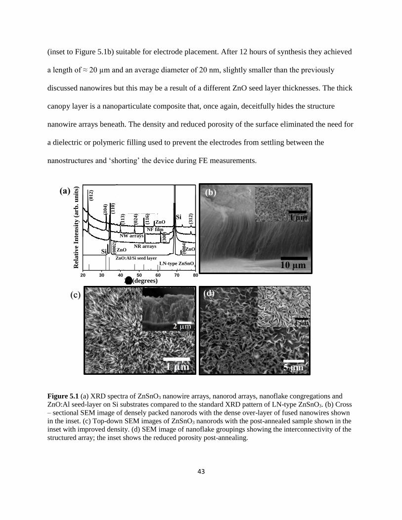
43
(inset to Figure 5.1b) suitable for electrode placement. After 12 hours of synthesis they achieved
a length of ≈ 20 µm and an average diameter of 20 nm, slightly smaller than the previously
discussed nanowires but this may be a result of a different ZnO seed layer thicknesses. The thick
canopy layer is a nanoparticulate composite that, once again, deceitfully hides the structure
nanowire arrays beneath. The density and reduced porosity of the surface eliminated the need for
a dielectric or polymeric filling used to prevent the electrodes from settling between the
nanostructures and ‘shorting’ the device during FE measurements.
Figure 5.1 (a) XRD spectra of ZnSnO3 nanowire arrays, nanorod arrays, nanoflake congregations and
ZnO:Al seed-layer on Si substrates compared to the standard XRD pattern of LN-type ZnSnO3. (b) Cross
– sectional SEM image of densely packed nanorods with the dense over-layer of fused nanowires shown
in the inset. (c) Top-down SEM images of ZnSnO3 nanorods with the post-annealed sample shown in the
inset with improved density. (d) SEM image of nanoflake groupings showing the interconnectivity of the
structured array; the inset shows the reduced porosity post-annealing.
20 30 40 50 60 70 80
200 300 400 500 600
Si
297
E(L
O)
433
E(L
O)
E(L
O)
226
Inte
nsi
ty (
a.
u.)
Raman shift (cm-1
)
NF film
NW arrays
NR arrays
(012)
(312)
(300)
(116)
(113)
(024)(1
10)
(0002)
(0004)
(104)
ZnO
ZnOZnOSi
Si
Rel
ati
ve
Inte
nsi
ty (
arb
. u
nit
s)
ZnO:Al/Si seed layer
LN-type ZnSnO3
2 (degrees)
B
(a) (b)
(c) (c) (d)

44
The ZnSnO3 nanorod arrays, shown in Figure 5.1c were synthesized in a water/PEG
mixture and are randomly orientated with columns that narrow towards the top, the base has an
average diameter of 30 nm while the structure tapers to 5 nm at the tip with an overall structural
thickness of ~ 6 µm. The as-prepared sample was too porous to allow sputtering of the Pt top
electrodes which inhibits the ability for FE measurements; to increase the density of the nanorods
the sample was annealed for 6 hours at 200 °C. The inset to Figure 5.1c shows cross-sectional
SEM of the ZnSnO3 nanorod assembly with improved compactness and preserved nanorod
structures after annealing successfully allowing for the deposition of top electrodes and FE
measurements.
When the precursor solution is composed of 60/40 vol. % water/EG the resulting
structural growth is of nanoflakes, as shown in Figure 5.1d. The SEM image shows the
nanoflakes are 5 -10 nm thick and interconnected to each other. As with the nanorods, the flakes
were annealed to improve inter-structural density for 6 hours at 200 °C, seen in the inset to
Figure 5.1d; the film averaged 2 µm thick and porosity was decreased to < 10 vol. % post-
annealing making it suitable for FE measurements.
Improving the structural porosity enabled the design of thick film capacitors for FE
measurements from the ZnSnO3 nanostructured arrays without the need for dielectric fillers that
ultimately introduce dielectric losses during polarization testing by aiding in the deposition of the
top Pt electrodes. As previously, the doped ZnO layer served as the bottom electrode. The results
of FE measurements at room temperature with an applied voltage of 220 V are shown in Figure
5.2 of the LN-type ZnSnO3 partially aligned nanowire, nanorod, and nanoflakes arrays,
respectively. Of the three nanostructured arrays the nanowires had the highest remanent
polarization (Pr) (Figure 5.2a) of ≈ 28 µC/cm2 with an estimated coercive field (Ec) of ≈ 25

45
kV/cm calculated from the sample thickness of 20 μm determined by SEM (refer to Figure 5.1b).
The extrapolated spontaneous polarization at 220 V is ≈ 38 µC/cm2 giving the partially aligned
nanowire arrayed thick film hysteresis loop a squareness of ≈ 79 %. The FE measurements taken
from various top Pt electrodes and the same bottom ZnO:Al bottom electrode show similar
polarization values as a result of the uniform distribution of nanowires throughout the surface of
the substrate.
Figure 5.2 Ferroelectric hysteresis loops measured at room temperature from the Pt/ZnSnO3
nanostructure arrayed films/ZnO:Al capacitors using an applied voltage of 220 V of the (a) nanowires, (b)
nanorods, and (c) nanoflake groups.
The ZnSnO3 partially aligned nanowire arrays and nanoflake assemblies exhibited much
lower Pr values of ~ 11 µC/cm2 and 4.7 µC/cm2, respectively. The coercive fields were estimated
to be are ≈ 40 kV/cm for the nanorods and ≈ 38 kV/cm for the nanoflakes based on the
respective film thicknesses from SEM. The Pr values are significantly lower than the values
reported for epitaxial (111) ZnSnO3 nanostructured films (Pr = 47 µC/cm2) and is the subject of
future investigations while the coercive field values, especially for the nanowire arrayed film, are
much lower than those previously reported.[1] It is clear though that the partially aligned
nanowire arrays display far superior FE properties to those of the other nanostructures and holds
much potential as a suitable alternative to future Pb-free FE devices.
-100 -50 0 50 100
-40-30-20-10
010203040 NW arrays
Po
lari
zati
on
(
C/c
m2)
Electric Field (kV/cm)
-100 -50 0 50 100-30
-20
-10
0
10
20
30NR Arrays
Po
lari
zati
on
(
C/c
m2)
Electric Field (kV/cm)-100 -50 0 50 100
-15
-10
-5
0
5
10
15NF Assemblage
Po
lari
zati
on
(
C/c
m2)
Electric Field (kV/cm)
(a) (b) (c)

46
To summarize, by a strategic synthesis approach involving PLD and a solvothermal
process, LN-type ZnSnO3 partially aligned nanowire, nanorods, and nanoflakes were grown on
Si substrates due to the doped ZnO seed layer. This resulted in a densely packed, highly
crystalline film as a result of the similar crystal symmetry between the ZnO layer and LN-type
ZnSnO3. The fusing of the nanowire and the densely packed structures allowed for direct
measurement of FE properties while the nanorods and nanoflakes samples required low
temperature annealing to reduce porosity before electrodes could be deposited for testing. The
best Pr of 28 µC/cm2 at a low coercive field of 25 kV/cm was exhibited even by the partially
aligned nanowire arrays. Accounts of ferroelectricity in LN-type ZnSnO3 nanostructures have
not been well reported to date so this report could provide value insight into the design of future
FE devices centered around Pb-free materials.
5.1 References
[1] Y. Inaguma, M. Yoshida, T. Katsumata, J Am Chem Soc 130 (2008) 6704.

47
Chapter 6:
Summary and Future Work
Ferroelectric (FE) perovskites with switchable polarization properties are identified as
next generation ‘smart materials’, which can convert changes in mechanical energies into
electrical signals (piezoelectricity) and potentially provide faster, smaller, energy-efficient
systems that can manage, sense and store information efficiently (ferroelectricity). Despite
adverse environmental impact, lead-zirconium-titanate (PZT) has been the dominant component
in such applications. The aim of the work discussed in this thesis is to develop a novel synthesis
process to grow nanostructured films of lead-free FEs that functionally challenge the widely used
PZT and to acquire fundamental understanding of the new growth mechanism for extending the
process to a large-area growth capability in future. The high piezoelectric (PE) and FE properties
predicted and recently observed in environmentally benign, zinc-based perovskite-type oxide
ZnSnO3 has the potential to replace the current industry standard of lead-based ceramics.
Our research is aimed to advance the current state of research that aims to replace PZT in
a multitude of devices. The large-scale synthesis and integration of these materials with ordered
low-dimensional structures and controlled crystal orientations is a challenge due to the narrow
window of parameters for which the phases are stable. Our material synthesis scheme
encompasses a unique physical/chemical technique that include pulsed laser deposition (PLD)
and solvothermal processes to fabricate oriented nanostructure arrays on both hard and flexible
substrates. Initially nanograined seed layers of oriented zinc oxide thin-films were deposited on
the substrates by the PLD process, which were then chemically reacted in controlled ionic

48
precursor environment to promote the stabilization and growth of the desired nanostructured
phases. We are the first to demonstrate a generalized scale-up synthesis scheme for Pb-free and
earth-abundant elements based ZnSnO3, as different dimensional nanostructure arrays on
industrially viable hard substrates. We investigated their structure-dependent FE properties and
developed a fundamental understanding of the structure, stability and growth of these hitherto
unexplored perovskite material in nanostructured forms to help in designing next-generation
high-performance ferro- and piezo-devices.
Zinc stannate is also a direct band gap material (2.42 eV) that may have light-harvesting
applications if the band gap can be reduced to a level where it can absorb the full solar
spectrum.[1] Future work would focus on band gap tuning by introducing dopants into the
crystal structure as in this material the band gap is a strong function of the lattice constants. The
FE photovoltaics are unique in that it is the inherent polarization that drives photocurrent
throughout the device and improves charge separation efficiency.[2]
6.1 References
[1] H. Gou, F. Gao, J. Zhang, Computational Materials Science 49 (2010) 552.
[2] Y. Yuan, Z. Xiao, B. Yang, J. Huang, Journal of Materials Chemistry A 2 (2014) 6027.

49
Appendices
Appendix 1: Publication List
The work presented in this dissertation is based in part on the following journal articles:
1.1 Peer-Reviewed Journal Articles
1. Devajyoti Mukherjee, Anuja Datta, Corisa Kons, Mahesh Hordagoda, Sarath Witanachchi and
Pritish Mukherjee, “Intrinsic anomalous ferroelectricity in vertically-aligned LiNbO3-type
ZnSnO3 hybrid nanoparticle-nanowire arrays” Applied Physics Letters 2014 (105) 212903
2. Anuja Datta, Corisa Kons, Devajyoti Mukherjee, Sarath Witanachchi and Pritish Mukherjee,
“Evidence of superior ferroelectricity in aligned ZnSnO3 nanowire arrays” Small 2014 (10) 4093
1.2 Peer-Reviewed Conference Proceedings
1. “Measurements of Polarization Switching in LiNbO3-type ZnSnO3/ZnO Nanocomposite Thin
Films”D Mukherjee, M Hordagoda, C Kons, A Datta, S Witanachchi, P. Mukherjee, Fall MRS
Proceedings 1729, mrsf14-1729-m11-07 (2015).
2. “Ferroelectricity in Strategically Synthesized Pb-Free LiNbO3-type ZnSnO3 Nanostructure
Arrayed Thick Films”. Anuja Datta, Devajyoti Mukherjee, Corisa Kons, Sarath Witanachchi and
Pritish Mukherjee, Fall MRS Proceedings 1729, mrsf14-1729-m11-02 (2015).
3. “Facile Growth of Functional Perovskite Oxide Nanowire Arrays by Hybrid Physical-Chemical
Techniques”. Corisa Kons, and Anuja Datta, MRS Proceedings 1751, mrsf14-1751-ll13-07
(2015).
1.3 Conference Presentations
1. Corisa Kons, Anuja Datta, Devajyoti Mukherjee , Pritish Mukherjee “Band Gap Tuning in ZnSnO3
Nanorods by Cation Doping and Core-Shell Method for Solar Cell Applications” Florida Annual Meeting
and Exposition (FAME) by the Florida Section of the American Chemical Society, Innisbrook,
Florida, May 7 – 9, 2015.
2. Corisa Kons, Anuja Datta, Pritish Mukherjee, “Band-Gap Tuning in Perovskite-type Ferroelectric
ZnSnO3 by Doping and Core-Shell Approach for Solar Cell Applications” American Physical
Society, Session L34: Thin Film Photovoltaics (Perovskites, etc), March 4, 2015.
3. Anuja Datta, Devajyoti Mukherjee, Corisa Kons, Sarath Witanachchii, and Pritish Mukherjee,
“Ferroelectricity in Strategically Synthesized Pb-free LiNbO3-type ZnSnO3 Nanostructure

50
Arrayed Thick Films” 2014 MRS Fall Meeting & Exhibit, Boston, MA, November 30 -
December 5, 2014.
4. Corisa Kons and Anuja Datta, “Facile Growth of Functional Perovskite Oxide Nanowire Arrays
by Hybrid Physical-Chemical Techniques” 2014 MRS Fall Meeting & Exhibit, Boston, MA,
November 30 - December 5, 2014.
5. Mahesh Hordagoda, Corisa Kons, Devajyoti Mukherjee, Anuja Datta, Sarath Witanachchi1, and
Pritish Mukherjee, “Evidence of Polarization Switching in LiNbO3-Type ZnSnO3/ZnO
Nanocomposite Thin Films” 2014 MRS Fall Meeting & Exhibit, Boston, MA, November 30 -
December 5, 2014.
6. Corisa Kons, Anuja Datta, Devajyoti Mukherjee, and Pritish Mukherjee “Band Engineering in
ZnSnO3 Nanorods by Doping and Core-Shell Approach for Solar Cell Applications” 2014 MRS
Fall Meeting & Exhibit, Boston, MA, November 30 - December 5, 2014.
7. Corisa Kons, Anuja Datta, Devajyoti Mukherjee, and Pritish Mukherjee, “Band Gap
Modification in ZnSnO3 by Cation Doping and Core-Shell Approach for Solar Cell Applications”
NanoFlorida 2014 - The 7th Annual Nanoscience Technology Symposium Sept. 25-26, Miami,
Fl, USA, 2014.
8. Boeing Smith, Corisa Kons, and Anuja Datta, “Band Energy Modification of Ferroelectric
ZnSnO3 for Photovoltaic Applications” REU-RET Poster Symposium, University of South
Florida, July 31, Tampa, Fl, USA, 2014.
9. Corisa Kons and Anuja Datta “Seed-Assisted Synthesis and Characterization of Ferroelectric
ZnSnO3 Nanostructures” Florida Annual Meeting and Exposition (FAME) by the Florida Section
of the American Chemical Society, Innisbrook, Florida, May 8 – 10, 2014.
10. Corisa Kons and Anuja Datta, “Growth and Characterization of Eco-friendly Lead-Free
Ferroelectric ZnSnO3 Nanostructures” 38th International Conference & Exposition on Advanced
Ceramics & Composites, Daytona Beach, Florida, January 26-31, 2014

51
Appendix 2: Copyright Permissions
Excerpts from the license agreements for use of material from previously published articles are
reproduced below.
JOHN WILEY AND SONS LICENSE
TERMS AND CONDITIONS
Jul 29, 2015
This Agreement between Corisa Kons ("You") and John Wiley and Sons ("John Wiley and
Sons") consists of your license details and the terms and conditions provided by John Wiley
and Sons and Copyright Clearance Center.
License Number 3678320890919
License date Jul 29, 2015
Licensed Content Publisher John Wiley and Sons
Licensed Content
Publication Small
Licensed Content Title Evidence of Superior Ferroelectricity in Structurally Welded
ZnSnO3 Nanowire Arrays
Licensed Content Author Anuja Datta,Devajyoti Mukherjee,Corisa Kons,Sarath
Witanachchi,Pritish Mukherjee
Licensed Content Date Jun 23, 2014
Pages 7
Type of Use Dissertation/Thesis
Requestor type Author of this Wiley article
Format Print and electronic
Portion Text extract
Number of Pages 12
Will you be translating? No
Title of your thesis /
dissertation
Synthesis, Characterization and Ferroelectric Properties of LN-
Type ZnSnO3 Nanostructures
Expected completion date Aug 2015
Expected size (number of
pages) 51
AIP PUBLISHING LLC LICENSE
TERMS AND CONDITIONS
Jul 29, 2015

52
All payments must be made in full to CCC. For payment instructions, please see
information listed at the bottom of this form.
License Number 3678351131548
Order Date Jul 29, 2015
Publisher AIP Publishing LLC
Publication Applied Physics Letters
Article Title Intrinsic anomalous ferroelectricity in vertically aligned LiNbO3-
type ZnSnO3 hybrid nanoparticle-nanowire arrays
Author Devajyoti Mukherjee,Anuja Datta,Corisa Kons, et al.
Online Publication Date Nov 25, 2014
Volume number 105
Issue number 21
Type of Use Thesis/Dissertation
Requestor type Author (original article)
Format Print and electronic
Portion Figure/Table
Number of figures/tables 6
Title of your thesis /
dissertation
Synthesis, Characterization and Ferroelectric Properties of LN-
Type ZnSnO3 Nanostructures
Expected completion
date Aug 2015
Estimated size (number
of pages) 51
Total 0.00 USD
Terms and Conditions
AIP Publishing LLC -- Terms and Conditions: Permissions Uses
AIP Publishing LLC ("AIPP"") hereby grants to you the non-exclusive right and license to
use and/or distribute the Material according to the use specified in your order, on a one-time
basis, for the specified term, with a maximum distribution equal to the number that you have
ordered. Any links or other content accompanying the Material are not the subject of this
license.

53
CAMBRIDGE UNIVERSITY PRESS LICENSE
TERMS AND CONDITIONS
Jul 29, 2015
This is a License Agreement between Corisa Kons ("You") and Cambridge University Press
("Cambridge University Press") provided by Copyright Clearance Center ("CCC"). The
license consists of your order details, the terms and conditions provided by Cambridge
University Press, and the payment terms and conditions.
All payments must be made in full to CCC. For payment instructions, please see
information listed at the bottom of this form.
License Number 3678360356172
License date Jul 29, 2015
Licensed content publisher Cambridge University Press
Licensed content publication MRS Online Proceedings Library
Licensed content title
Facile Growth of Functional Perovskite
Oxide Nanowire Arrays by Hybrid
Physical-Chemical Techniques
Licensed content author Corisa Kons and Anuja Datta
Licensed content date Feb 10, 2015
Volume number 1751
Issue number -1
Type of Use
Requestor type
Portion Dissertation/Thesis
Author of this Cambridge University Press
article Author
Author / editor of the new work Full article
Title of your thesis / dissertation Yes
Expected completion date Yes
Estimated size(pages)
Synthesis, Characterization and
Ferroelectric Properties of LN-Type
ZnSnO3 Nanostructures

54
ROYAL SOCIETY OF CHEMISTRY LICENSE
TERMS AND CONDITIONS
Jul 29, 2015
This is a License Agreement between Corisa Kons ("You") and Royal Society of Chemistry
("Royal Society of Chemistry") provided by Copyright Clearance Center ("CCC"). The
license consists of your order details, the terms and conditions provided by Royal Society of
Chemistry, and the payment terms and conditions.
All payments must be made in full to CCC. For payment instructions, please see
information listed at the bottom of this form.
License Number 3678360827669
License date Jul 29, 2015
Licensed content publisher Royal Society of Chemistry
Licensed content publication Journal of Materials
Chemistry C
Licensed content title
Ferroelectric nanoparticles,
wires and tubes: synthesis,
characterisation and
applications
Licensed content author Justin Varghese,Roger W.
Whatmore,Justin D. Holmes
Licensed content date Feb 11, 2013
Volume number 1
Issue number 15
Type of Use Thesis/Dissertation
Requestor type academic/educational
Portion figures/tables/images
Number of figures/tables/images 1
Format print and electronic
Distribution quantity 10000
Will you be translating? no
Order reference number None
Title of the thesis/dissertation
Synthesis, Characterization
and Ferroelectric Properties
of LN-Type ZnSnO3
Nanostructures
Expected completion date Aug 2015
Estimated size 51

55
ELSEVIER LICENSE
TERMS AND CONDITIONS
Aug 02, 2015
This is a License Agreement between Corisa Kons ("You") and Elsevier ("Elsevier")
provided by Copyright Clearance Center ("CCC"). The license consists of your order details,
the terms and conditions provided by Elsevier, and the payment terms and conditions.
All payments must be made in full to CCC. For payment instructions, please see
information listed at the bottom of this form.
Supplier
Elsevier Limited
The Boulevard,Langford Lane
Kidlington,Oxford,OX5 1GB,UK
Registered Company Number 1982084
Customer name Corisa Kons
Customer address 3239 bainbridge dr
HOLIDAY, FL 34691
License number 3680940647033
License date Aug 02, 2015
Licensed content publisher Elsevier
Licensed content publication Solid State Communications
Licensed content title First-principles study of structural, electronic,
and optical properties of ZnSnO3
Licensed content author Hai Wang,Haitao Huang,Biao Wang
Licensed content date November 2009
Licensed content volume number 149
Licensed content issue number 41-42
Number of pages 4
Start Page 1849
End Page 1852
Type of Use reuse in a thesis/dissertation
Portion figures/tables/illustrations
Number of figures/tables/illustrations 1
Format both print and electronic
Are you the author of this Elsevier article? No
Will you be translating? No
Title of your thesis/dissertation Synthesis, Characterization and Ferroelectric
Properties of LN-Type ZnSnO3 Nanostructures