Federico Alessio Università degli Studi di Torino An Italian on … Time.
40
Federico Alessio Università degli Studi di Torino An Italian on An Italian on … … Time Time
-
Upload
maximillian-harris -
Category
Documents
-
view
218 -
download
1
Transcript of Federico Alessio Università degli Studi di Torino An Italian on … Time.

Federico AlessioUniversità degli Studi di Torino
An Italian on An Italian on … …
Time Time

Federico Alessio 08/02/2008 2
Way before CERN…
3rd February 1983
Now
Born in Torino – one week after schedule and under the snow…
Physics Department distance = 24 m (± 1)
One of my grandfathers was born in Lyon, the other one in Pennsylvania: none of them actually got a foreign passport, so I am definitely ITALIAN
Federico Alessio 08/02/2008 3
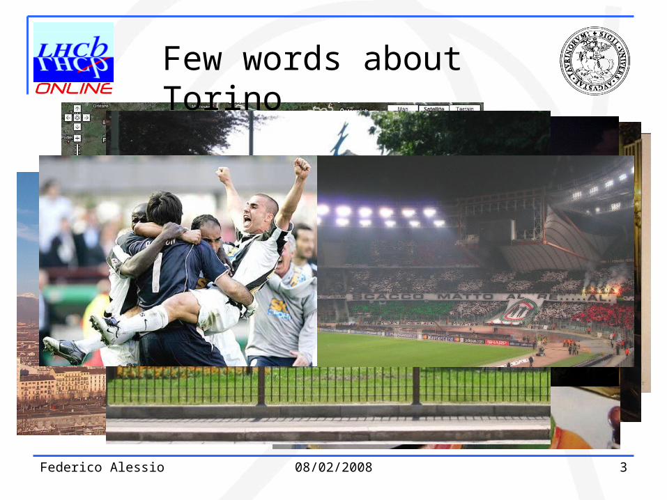
Few words about Torino
... Sweden won the men’s hockey gold medal...
Federico Alessio 08/02/2008 4
Just before CERN…
… for 14 years …
Now
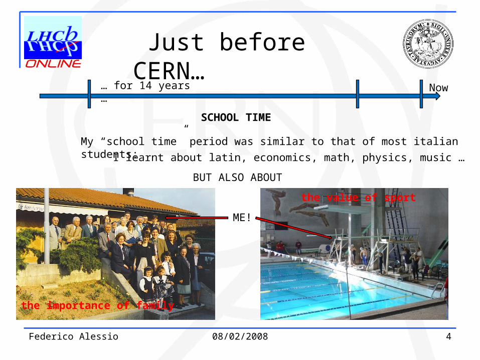
SCHOOL TIME
My “school time” period was similar to that of most italian students:
I learnt about latin, economics, math, physics, music …
BUT ALSO ABOUT
the importance of family
ME!
the value of sport

Federico Alessio 08/02/2008 5
Just before CERN…
… for 14 years …
Now
SCHOOL TIME
… AND
ME!
how to produce wine from grapes
how to build houses
how to play footballEverything has been very
useful and definitely necessary to reach CERN…

Federico Alessio 08/02/2008 6
Almost at CERN…2002 Now
UNIVERSITY TIME
University of Torino, Physics Department :
Bachelor degree in Physics in September 2005
2005
Thesis: “Study and characterization of front-end amplifiers in SiGe technology”
At the end of 2004, I was part of one of those school groups that come to CERN on a holiday trip basically to just waste some time having fun and playing with lead/glass scintillators in front of the old DELPHI detector... but, I was very interested and when I saw the big red magnet of CMS parked in point 5, I decided to study Physics. Maybe reaching CERN one day…
Unfortunately I don’t have pictures that represent that crucial moment.

Federico Alessio 08/02/2008 7
Some work before CERN
For my bachelor thesis, I spent 5 months in the Microelectronics Lab in Torino studying and (trying to) design(ing) front-end amplifiers in Si/SiGe CMOS/BiCMOS technologies.
First design of a generic (and simple) front-end amplifier (Charge-Sensitive Amplifier) using Sun-Cadence software
CMOS Technology: n-type and p-type MOSFET in the same semiconductor substrate
HBT BiCMOS Technology: n-type and p-type MOSFET and BJT transistors in the same semiconductor substrate
Compared to...

Federico Alessio 08/02/2008 8
Some work before CERN
The mixed technology benefits from the merits of the CMOS transistors and the BJT transistors
High device density due to the use of BJT only in crucial places
Higher gain-bandwidth product
Better performance (faster)
Lower power consumption
Higher semplicity of production
Perfect to design amplifiers to process very fast signals with a high amplification at higher frequency and lower power consumption than usual MOSFETs FE op-amps
Even better results if Ge grown on Si:
Si used just as substrate, Ge used for actual conduction of e-
Lower energy gap for conduction, lower consumption, better performances
Faster = 4 ns for 1000 fC signal
Bigger amplification, up to 25 K times
Higher bandwidth, up to 10 GHz
Linearity respected
Federico Alessio 08/02/2008 9
Some work before CERN
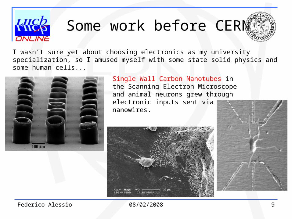
I wasn’t sure yet about choosing electronics as my university specialization, so I amused myself with some state solid physics and some human cells...
Single Wall Carbon Nanotubes in the Scanning Electron Microscope and animal neurons grew through electronic inputs sent via nanowires.
Federico Alessio 08/02/2008 10
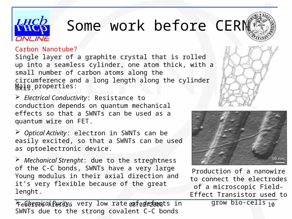
Some work before CERNCarbon Nanotube? Single layer of a graphite crystal that is rolled up into a seamless cylinder, one atom thick, with a small number of carbon atoms along the circumference and a long length along the cylinder axis.Main properties:
Electrical Conductivity: Resistance to conduction depends on quantum mechanical effects so that a SWNTs can be used as a quantum wire on FET.
Optical Activity: electron in SWNTs can be easily excited, so that a SWNTs can be used as optoelectronic device.
Mechanical Strenght: due to the streghtness of the C-C bonds, SWNTs have a very large Young modulus in their axial direction and it’s very flexible because of the great lenght.
Chemical Purity: very low rate of defects in SWNTs due to the strong covalent C-C bonds
Production of a nanowire to connect the electrodes of a
microscopic Field-Effect Transistor used to grow bio-
cells

Federico Alessio 08/02/2008 11
Finally at CERN…Now
SUMMER STUDENT
4 july – 29 september 2006
... I was selected by Roberto Campagnolo to take part in the commissioning of the TPC of ALICE experiment, but I was involved in many other activities:
assembling electronics boards and removing non-working boards directly in point 2
being active part of the data analysis of a good number of FE electronics board of the TPC using root
joining many briefing meeting of the TPC ALICE group in order to have the first impression of the importance of meeting ( ... )
having the opportunity to learn VERILOG and VHDL and to work directly on a programmable FPGA on which I could “play” by myself
Implementation of a Trigger Adapter Module
in Verilog
Master Degree in Electronics Engeneering and ...
Federico Alessio 08/02/2008 12
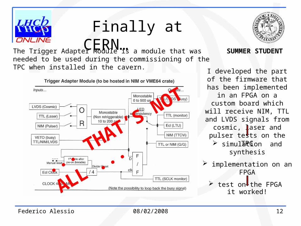
Finally at CERN…SUMMER STUDENTThe Trigger Adapter Module is a module that was needed to
be used during the commissioning of the TPC when installed in the cavern.
I developed the part of the firmware that has
been implemented in an FPGA on a custom board which will receive NIM, TTL and LVDS signals
from cosmic, laser and pulser tests on the TPC
simulation and synthesis
implementation on an FPGA
test on the FPGA it worked!
... THAT’S NOT ALL ...

Federico Alessio 08/02/2008 13
Finally at CERN…SUMMER STUDENTI met my friends after 22 hours I reached CERN and of
course we enjoyed the World Cup (and not only) at Charly’s...

Federico Alessio 08/02/2008 14
Finally at CERN…SUMMER STUDENTI proudly organized the CERN Summer Football
Tournament in front of building 40 ...
They were in LHCb
She is in LHCb

Federico Alessio 08/02/2008 15
Finally at CERN…SUMMER STUDENT
I met people from everywhere and people of any culture and type ...

Federico Alessio 08/02/2008 16
1 February 2007 Now
TECHNICAL STUDENTRichard selected me to alleviate the amount of work that he had to face during the
past year…
Finally at CERN…
“Official” proposal of working on the coarse and fine time alignment of the experiment. The project involves the development of an electronics monitor board (Beam Phase and Intensity Monitor) for precise bunch-by-bunch measurements of the intensity and the phase of the LHC beams involving both analogue and digital electronics, and the development of GUI interfaces to monitor the information. Moreover, the control of a new system (RF2TTC System) provided by the LHC group has to be implemented to distribute the clock to the whole TFC system and then to the experiment. A User Interface will help the users to interact with the systems.
I have been also proposed to be active part of the installing, commissioning and support of the whole TFC system and I to take part to some sessions of the global LHCb commissioning.
Master Thesis: “A complete system for monitoring and controlling the timing of the LHCb experiment”
Federico Alessio 08/02/2008 17
Motivations: LHCb Timing
Aid in the coarse and fine time alignment of the experiment
Monitor individual bunch position Measure bunch intensity bunch-by-bunch for trigger
conditions Measure bunch phase bunch-by-bunch for long-term
stability in clock distribution
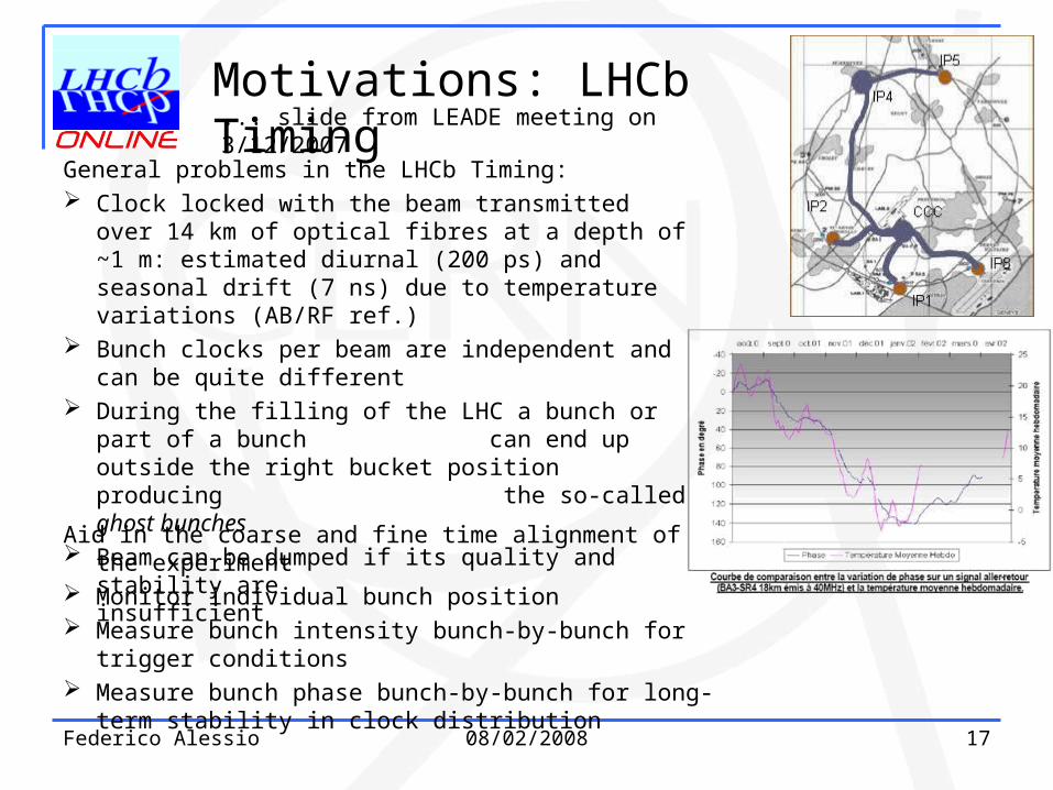
General problems in the LHCb Timing: Clock locked with the beam transmitted over 14
km of optical fibres at a depth of ~1 m: estimated diurnal (200 ps) and seasonal drift (7 ns) due to temperature variations (AB/RF ref.)
Bunch clocks per beam are independent and can be quite different
During the filling of the LHC a bunch or part of a bunch can end up outside the right bucket position producing the so-called ghost bunches
Beam can be dumped if its quality and stability are insufficient
... slide from LEADE meeting on 3/12/2007
Federico Alessio 08/02/2008 18
Project: BPIM + RF2TTC
Proposal of a complete system to monitor, control, and time align LHCb experiment
Gives a clear structure of the beam injected taking the bipolar pulse coming from BPTX
Determines the position of the orbit locally and monitors the clock phase with respect to the bunch passing through the detector
Determines the exact trigger conditions for sampling events in the detector and determines the exact trigger conditions for significant events or not, checking whether the detector samples a bunch with protons or an empty bunch
Produces a relative measure of the intensities of bunches
Produces an empty crossing veto for the sampled events whenever a bunch is absent in the expected location
Searches for ghost bunches
Gives instantaneous information about the presence/absence of beam
Beam Phase and Intensity Monitor
RF2TTC System
Distributes the Bunch clocks and Orbit clocks to all the ODINs and therefore to all the FEE of each sub-detector
Able to convert, clean, synchronize and select the clocks for the experiment
Fine and coarse adjustments on the clock signals
Monitoring and controlling performed using a user-friendly GUI interface via the Experimental Control
System (ECS)
... slide from my thesis presentation on 21/12/2007
Federico Alessio 08/02/2008 19
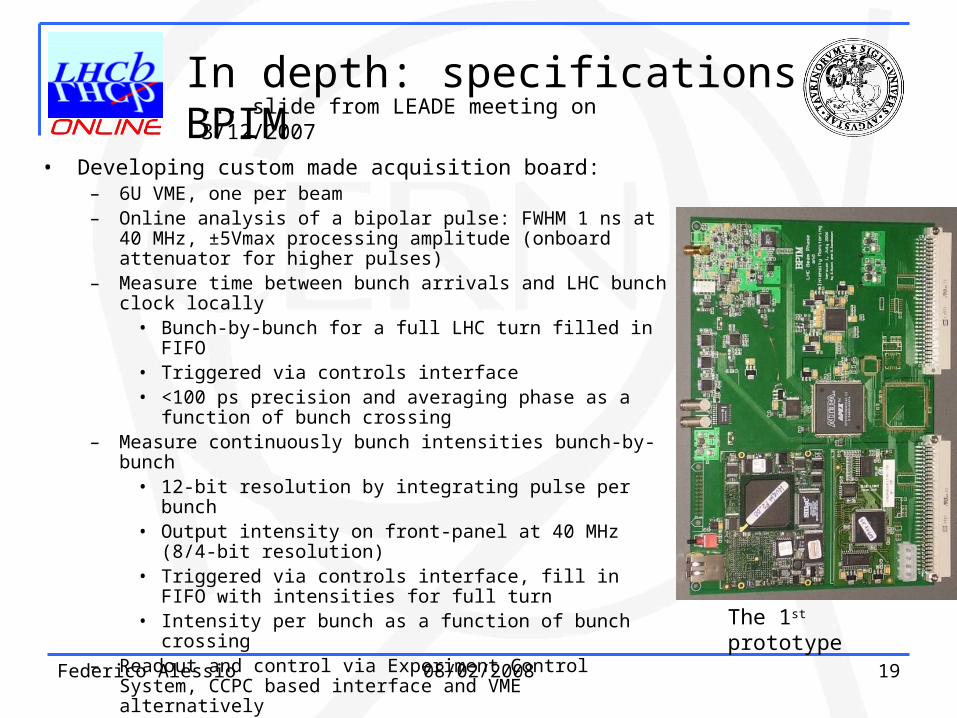
In depth: specifications of BPIM
The 1st prototype
• Developing custom made acquisition board:– 6U VME, one per beam– Online analysis of a bipolar pulse: FWHM 1 ns at 40 MHz,
±5Vmax processing amplitude (onboard attenuator for higher pulses)
– Measure time between bunch arrivals and LHC bunch clock locally
• Bunch-by-bunch for a full LHC turn filled in FIFO • Triggered via controls interface• <100 ps precision and averaging phase as a function
of bunch crossing– Measure continuously bunch intensities bunch-by-bunch
• 12-bit resolution by integrating pulse per bunch• Output intensity on front-panel at 40 MHz (8/4-bit
resolution)• Triggered via controls interface, fill in FIFO with
intensities for full turn• Intensity per bunch as a function of bunch crossing
– Readout and control via Experiment Control System, CCPC based interface and VME alternatively
– Interfaced directly to LHCb Timing and Fast Control system
– Data processing on FPGA
... slide from LEADE meeting on 3/12/2007
Federico Alessio 08/02/2008 20
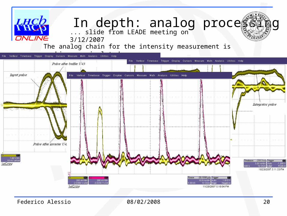
The analog chain for the intensity measurement is working as simulated
In depth: analog processing... slide from LEADE meeting on 3/12/2007

Federico Alessio 08/02/2008 21
The board has extensively been tested in laboratory …
Linearization to be performed in the FPGA during the data processing
Understanding of a TDC problem in order to improve the confidence on the distribution
In depth: performance in the lab... slide from LEADE meeting on 3/12/2007
Federico Alessio 08/02/2008 22
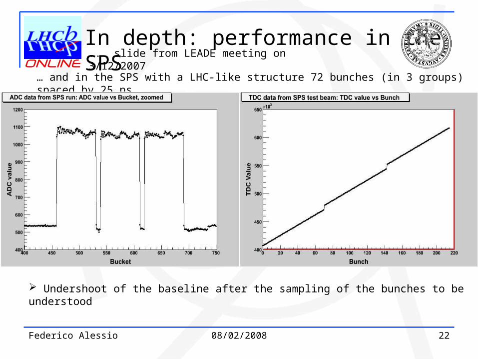
… and in the SPS with a LHC-like structure 72 bunches (in 3 groups) spaced by 25 ns.
Undershoot of the baseline after the sampling of the bunches to be understood
In depth: performance in the SPS... slide from LEADE meeting on 3/12/2007

Federico Alessio 08/02/2008 23
Crate controller: CAEN USB to VME interface
6U VMEx64 crateRF_Tx trasmitter: located in IP4, transmits the timing signals to the electronics
RF_Rx receiver: receives the timing signal from the RF_Tx
RF2TTC board: interface card between the receiver module and the TTC systems of the electronics
Clock Fanout: dual 1:18 ECL and 4 NIM
The LHC provides the Orbit clock and the Bunch clocks through the RF2TTC System
In depth: the RF2TTC system
The control system is completely developed and fully working: you’ll find it in the pit soon …
Federico Alessio 08/02/2008 24
The project is complete, fully working and is being installed and commissioned with the TFC system.
By means of the BPIM, the beam is monitored bunch-by-bunch in order to have a measurement of the phase of each single bunch clock with respect to the clock edge sent by the LHC. A bunch of second prototypes of the board are already under production and will be completely tested during January/February. The control system is being developed and will be tested with the second prototype in order to have a complete system.
By means of the RF2TTC system, the clock sent to the TFC system is controlled. Fine adjustments can be performed on the clock in order to time align the experiment and to let the experiment sample events at the optimal point taking into account all the possible causes which can eventually shift the clock.
Conclusions
The performance tests as well as the two test beams in the SPS gave successful results. The system will be then crucial for the timing of the LHCb, which can be monitored and controlled easily.
The project has been presented to the LHCb and to the technical committee LEADE (LHC Experimental Accelerator Data Exchange Working Group) receiving extremely positive feedback and comments. The other LHC experiment showed their interests: ALICE will receive a second fully tested prototype board during March 2008 to be used for the time alignment of the ALICE detector.
The multitasking features allow the system to be used, adapted, and installed in any experiments similar to the ones at the LHC at CERN.
... slide from my thesis presentation on 21/12/2007
... THAT’S NOT ALL ...
Federico Alessio 08/02/2008 25
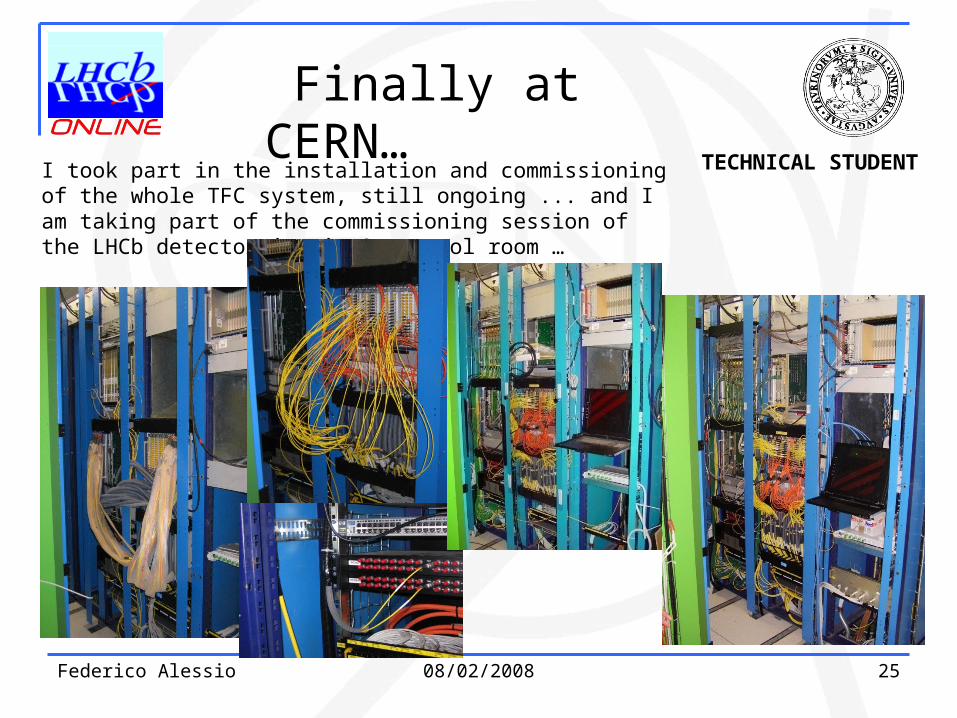
I took part in the installation and commissioning of the whole TFC system, still ongoing ... and I am taking part of the commissioning session of the LHCb detector in pit 8 control room …
TECHNICAL STUDENT
Finally at CERN…
Federico Alessio 08/02/2008 26
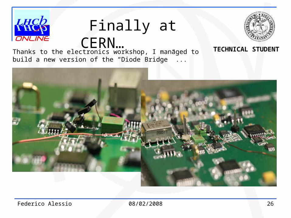
TECHNICAL STUDENTThanks to the electronics workshop, I managed to build a new version of the “Diode Bridge” ...
Finally at CERN…
Federico Alessio 08/02/2008 27
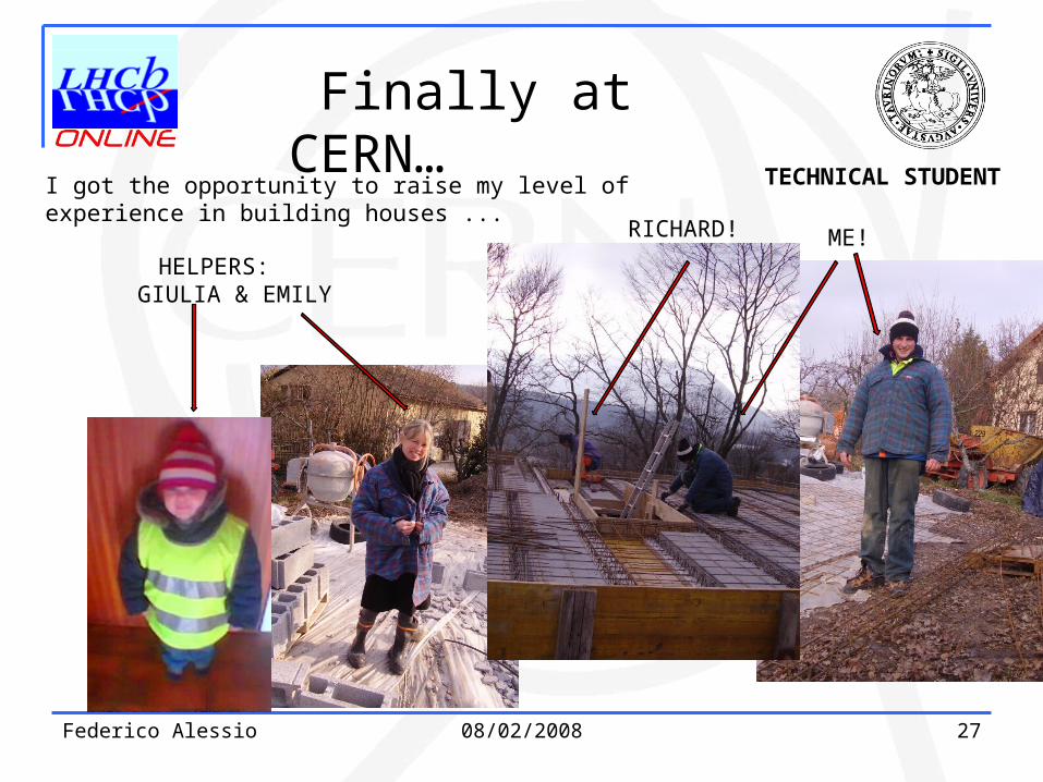
TECHNICAL STUDENTI got the opportunity to raise my level of experience in building houses ...
Finally at CERN…
ME!RICHARD!
HELPERS: GIULIA & EMILY
Federico Alessio 08/02/2008 28
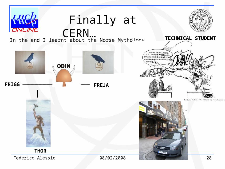
TECHNICAL STUDENTIn the end I learnt about the Norse Mythology...
Finally at CERN…
FRIGG FREJA
THOR

Federico Alessio 08/02/2008 29
Now
DOCTORAL STUDENT?
Does someone have a doctoral proposal and is willing to hire me?
(It’s not a joke, perhaps I’ll be here until the end of May)
After CERN…Future
Grazie per l’attenzione / Thanks for listening
Merci pour l’attention / Gracias para l’atencion
Danke für das Hören / Tack själv till deras uppmärksamhet
Federico Alessio 08/02/2008 30
extras
Federico Alessio 08/02/2008 31
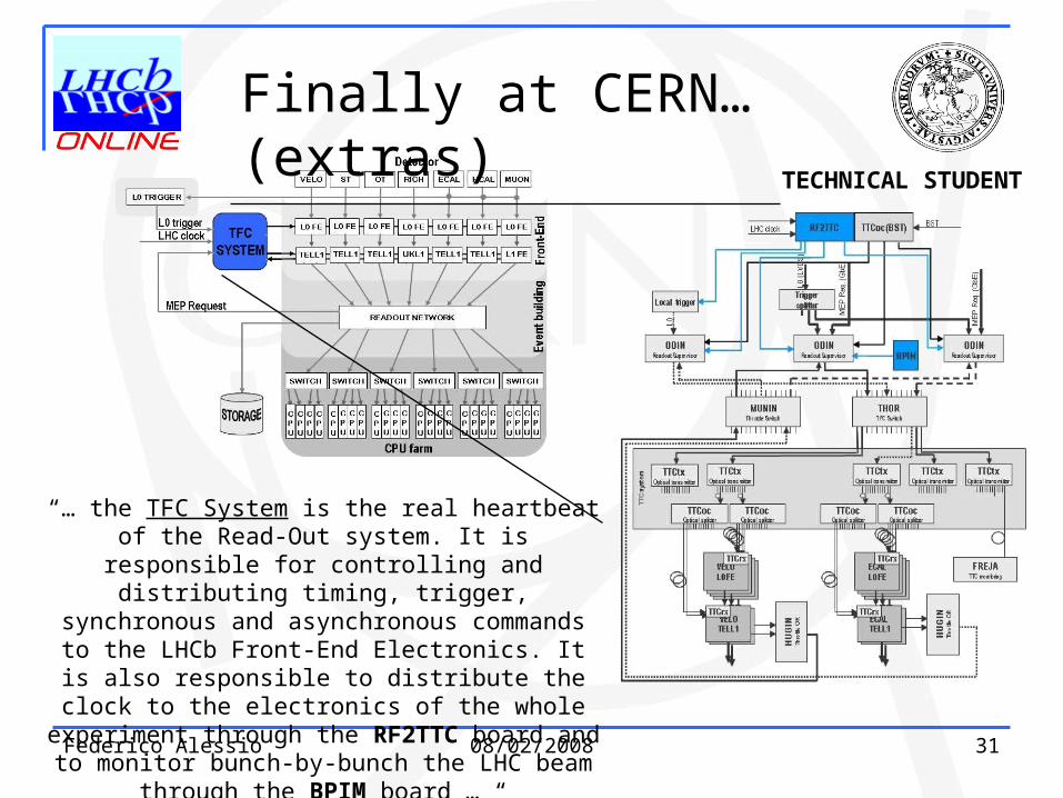
“… the TFC System is the real heartbeat of the Read-Out system. It is responsible for
controlling and distributing timing, trigger, synchronous and asynchronous commands to
the LHCb Front-End Electronics. It is also responsible to distribute the clock to the
electronics of the whole experiment through the RF2TTC board and to monitor bunch-by-bunch the LHC beam through the BPIM board
… “
TECHNICAL STUDENT
Finally at CERN… (extras)
Federico Alessio 08/02/2008 32
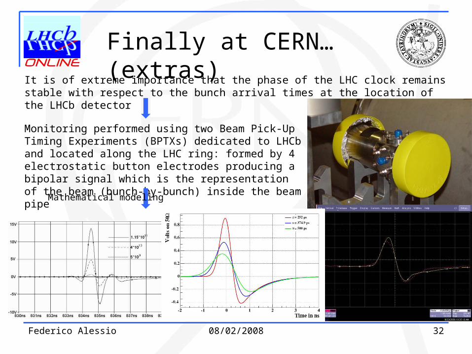
It is of extreme importance that the phase of the LHC clock remains stable with respect to the bunch arrival times at the location of the LHCb detector
Monitoring performed using two Beam Pick-Up Timing Experiments (BPTXs) dedicated to LHCb and located along the LHC ring: formed by 4 electrostatic button electrodes producing a bipolar signal which is the representation of the beam (bunch-by-bunch) inside the beam pipe
Mathematical modeling
Finally at CERN… (extras)
Federico Alessio 08/02/2008 33
MAIN FPGA
LVDSDrivers
BX InfoGP outputs
ADC
TDC
Integrator+
Rectifier(positive)
Rectifier(negative)
FPGA
AttenuatorAnalogbuffer
Beam
Threshold comparator
Zero-crossingcomparator
ThresholdDAC
FPGA
Delay
PECLF/F
Data
Clock
Delay
Reset
Dis
char
ge
Sample
Leveladapter
Bunchclock Programmable
delay
FPGA Clockfanout
DelayOne-shot
LVPECL/PECL
8:1 Divider
LVPECL/PECL
LVPECL/PECL
LVPECL/PECL
2:1 Divider
One-shot
Start
Stop
FIFOPhase
FIFOIntensity
Local Bus
VME interface (FPGA)
Drivers
Glue Card
Credit Card PC
VME Bus
EthernetOrbit Level
adapter
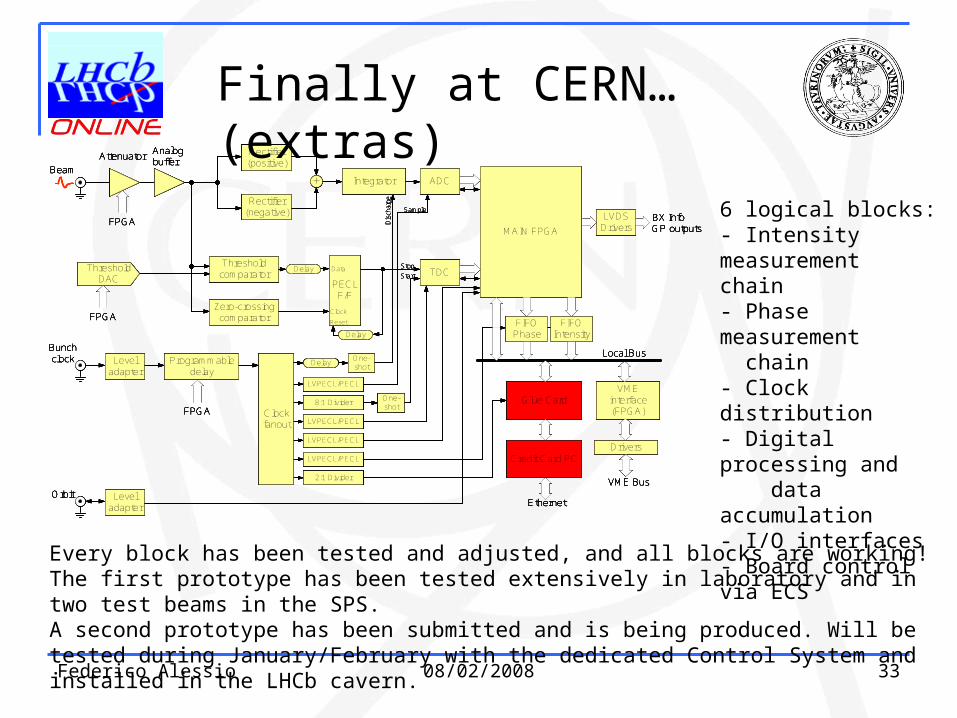
6 logical blocks:- Intensity measurement chain- Phase measurement chain- Clock distribution - Digital processing and data accumulation- I/O interfaces- Board control via ECS
Every block has been tested and adjusted, and all blocks are working! The first prototype has been tested extensively in laboratory and in two test beams in the SPS.A second prototype has been submitted and is being produced. Will be tested during January/February with the dedicated Control System and installed in the LHCb cavern.
Finally at CERN… (extras)

Federico Alessio 08/02/2008 34
The first prototype has been mounted and debugged in stages: a lot of modifications (thanks to the Mounting Workshop!) and understanding of the problems.
The analog chain is designed with current-feedback amplifiers: impressive slew rate and high gain-bandwith.
The stabilization of the rectifier chains has been a difficult task: the current feedback amplifiers are very unstable, but the best configuration has been found
New designs of the integrator have been implemented: improve stability, undershoot and baseline
Programmable attenuator fixed and constant-level-crossing method with programmable level (DAC)
Fixed Start and Stop signals for the TDC, still a problem with one mode of operation to be investigated with the manufactury (ACAM)
A lot of PECL – LVPECL and LVPECL – TTL translators implemented for improvements
Firmware written and implemented to control FIFOs for Intensity and Phase measurement
FIFOs are autonomous: each FIFO has its own RCLK, WCLK, OE, RENB, WENBThe board has very satisfactory performance!
Finally at CERN… (extras)
Federico Alessio 08/02/2008 35
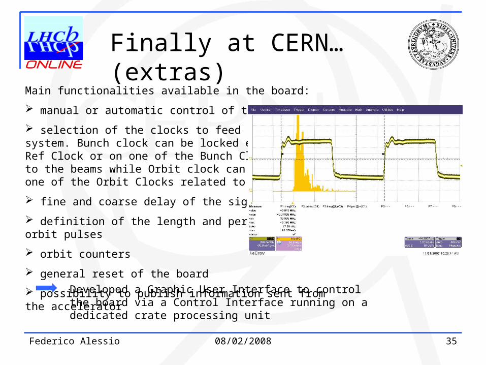
Main functionalities available in the board:
manual or automatic control of the board
selection of the clocks to feed to the TFC system. Bunch clock can be locked either on the Ref Clock or on one of the Bunch Clocks related to the beams while Orbit clock can be locked on one of the Orbit Clocks related to the beams
fine and coarse delay of the signals
definition of the length and period of the orbit pulses
orbit counters
general reset of the board
possibility to publish information sent from the acceleratorDeveloped a Graphic User Interface to control the board
via a Control Interface running on a dedicated crate processing unit
Finally at CERN… (extras)

Federico Alessio 08/02/2008 36
Main functionalities available in the board:
manual or automatic control of the board
selection of the clocks to feed to the TFC system. Bunch clock can be locked either on the Ref Clock or on one of the Bunch Clocks related to the beams while Orbit clock can be locked on one of the Orbit Clocks related to the beams
fine and coarse delay of the signals
definition of the length and period of the orbit pulses
orbit counters
general reset of the board
possibility to publish information sent from the acceleratorDeveloped a Graphic User Interface to control the board
via a Control Interface running on a dedicated crate processing unit
Finally at CERN… (extras)
Federico Alessio 08/02/2008 37
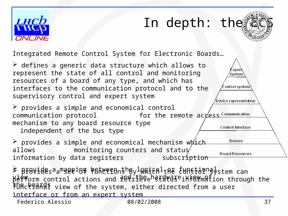
Integrated Remote Control System for Electronic Boards…
In depth: the ECS
defines a generic data structure which allows to represent the state of all control and monitoring resources of a board of any type, and which has interfaces to the communication protocol and to the supervisory control and expert system
provides a simple and economical control communication protocol for the remote access mechanism to any board resource type independent of the bus type
provides a simple and economical mechanism which allows monitoring counters and status information by data registers subscription
provide a mapping between the logical or functional view and the hardware view of the boards provides a set of functions by which the control system can perform control actions and retrieve status information through the functional view of the system, either directed from a user interface or from an expert system
Federico Alessio 08/02/2008 38
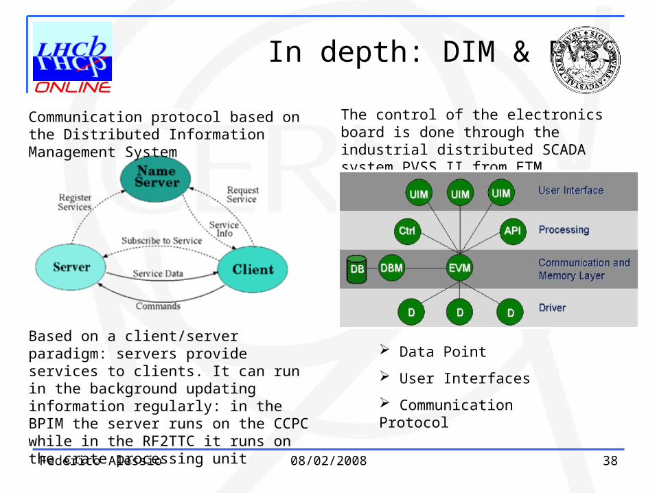
Communication protocol based on the Distributed Information Management System
Based on a client/server paradigm: servers provide services to clients. It can run in the background updating information regularly: in the BPIM the server runs on the CCPC while in the RF2TTC it runs on the crate processing unit
The control of the electronics board is done through the industrial distributed SCADA system PVSS II from ETM
In depth: DIM & PVSS
Data Point
User Interfaces
Communication Protocol
Federico Alessio 08/02/2008 39
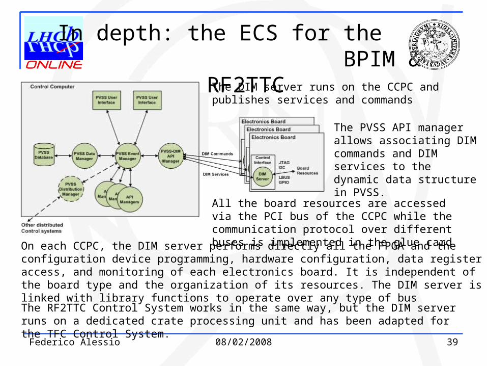
In depth: the ECS for the BPIM & RF2TTC
The DIM server runs on the CCPC and publishes services and commands
The PVSS API manager allows associating DIM commands and DIM services to the dynamic data structure in PVSS.
All the board resources are accessed via the PCI bus of the CCPC while the communication protocol over different buses is implemented in the glue cardOn each CCPC, the DIM server performs directly all the FPGA and the configuration
device programming, hardware configuration, data register access, and monitoring of each electronics board. It is independent of the board type and the organization of its resources. The DIM server is linked with library functions to operate over any type of busThe RF2TTC Control System works in the same way, but the DIM server runs on a dedicated crate processing unit and has been adapted for the TFC Control System.

Federico Alessio 08/02/2008 40
The control system for the RF2TTC is completely developed and fully working
In depth: the ECS for the BPIM & RF2TTC
The control system for the BPIM is under development and will be completed and tested with the second prototype of the board
Display Readings
Parameter Readings
Register Readings
UpdateRegister Structure
Parameter Settings
ReadWriteStructure
Register Settings
Control System
TranslationParam Regs
for FuncBlock
Display Settings
TranslationRegs Params
Automaticcomparison
GUI
SERVERRead->Set->Write->Read to hardware
Service(UpdateRegisters)
Command(ReadWriteRegisters)
Control Interface
Control network
Expert system
“Apply”
“Apply”