
Factoring Large Numbers with the TWIRL Devicetromer/papers/twirl.pdfFactoring Large Numbers with the...
26
Factoring Large Numbers with the TWIRL Device Adi Shamir and Eran Tromer Department of Computer Science and Applied Mathematics Weizmann Institute of Science, Rehovot 76100, Israel {shamir,tromer}@wisdom.weizmann.ac.il Abstract. The security of the RSA cryptosystem depends on the difficulty of factoring large integers. The best current factoring algorithm is the Number Field Sieve (NFS), and its most difficult part is the sieving step. In 1999 a large distributed computation involving hundreds of workstations working for many months managed to factor a 512-bit RSA key, but 1024- bit keys were believed to be safe for the next 15-20 years. In this paper we describe a new hardware implementation of the NFS sieving step (based on standard 0.13μm, 1GHz silicon VLSI technology) which is 3-4 orders of magnitude more cost effective than the best previously published designs (such as the optoelectronic TWINKLE and the mesh-based sieving). Based on a detailed analysis of all the critical components (but without an actual implementation), we believe that the NFS sieving step for 512-bit RSA keys can be completed in less than ten minutes by a $10K device. For 1024-bit RSA keys, analysis of the NFS parameters (backed by experimental data where possible) suggests that sieving step can be completed in less than a year by a $10M device. Coupled with recent results about the cost of the NFS matrix step, this raises some concerns about the security of this key size. 1 Introduction The hardness of integer factorization is a central cryptographic assumption and forms the basis of several widely deployed cryptosystems. The best integer factorization algorithm known is the Number Field Sieve [12], which was successfully used to factor 512-bit and 530-bit RSA moduli [5,1]. However, it appears that a PC-based implementation of the NFS cannot practically scale much further, and specifically its cost for 1024-bit composites is prohibitive. Recently, the prospect of using custom hardware for the computationally expensive steps of the Number Field Sieve has gained much attention. While mesh-based circuits for the matrix step have rendered that step quite feasible for 1024-bit compos- ites [3,16], the situation is less clear concerning the sieving step. Several sieving devices have been proposed, including TWINKLE [19,15] and a mesh-based circuit [7], but appar- ently none of these can practically handle 1024-bit composites. One lesson learned from Bernstein’s mesh-based circuit for the matrix step [3] is that it is inefficient to have memory cells that are ”simply sitting around, twiddling their thumbs” — if merely storing the input is expensive, we should utilize it efficiently by appropriate parallelization. We propose a new device that combines this intuition with the TWINKLE- like approach of exchanging time and space. Whereas TWINKLE tests sieve location one by one serially, the new device handles thousands of sieve locations in parallel at every clock cycle. In addition, it is smaller and easier to construct: for 512-bit composites we can
Transcript of Factoring Large Numbers with the TWIRL Devicetromer/papers/twirl.pdfFactoring Large Numbers with the...
Factoring Large Numbers with the TWIRL Device
Adi Shamir and Eran Tromer
Department of Computer Science and Applied MathematicsWeizmann Institute of Science, Rehovot 76100, Israel
shamir,[email protected]
Abstract. The security of the RSA cryptosystem depends on the difficulty of factoring largeintegers. The best current factoring algorithm is the Number Field Sieve (NFS), and its mostdifficult part is the sieving step. In 1999 a large distributed computation involving hundredsof workstations working for many months managed to factor a 512-bit RSA key, but 1024-bit keys were believed to be safe for the next 15-20 years. In this paper we describe a newhardware implementation of the NFS sieving step (based on standard 0.13µm, 1GHz siliconVLSI technology) which is 3-4 orders of magnitude more cost effective than the best previouslypublished designs (such as the optoelectronic TWINKLE and the mesh-based sieving). Basedon a detailed analysis of all the critical components (but without an actual implementation),we believe that the NFS sieving step for 512-bit RSA keys can be completed in less than tenminutes by a $10K device. For 1024-bit RSA keys, analysis of the NFS parameters (backedby experimental data where possible) suggests that sieving step can be completed in less thana year by a $10M device. Coupled with recent results about the cost of the NFS matrix step,this raises some concerns about the security of this key size.
1 Introduction
The hardness of integer factorization is a central cryptographic assumption and forms thebasis of several widely deployed cryptosystems. The best integer factorization algorithmknown is the Number Field Sieve [12], which was successfully used to factor 512-bit and530-bit RSA moduli [5,1]. However, it appears that a PC-based implementation of theNFS cannot practically scale much further, and specifically its cost for 1024-bit compositesis prohibitive. Recently, the prospect of using custom hardware for the computationallyexpensive steps of the Number Field Sieve has gained much attention. While mesh-basedcircuits for the matrix step have rendered that step quite feasible for 1024-bit compos-ites [3,16], the situation is less clear concerning the sieving step. Several sieving deviceshave been proposed, including TWINKLE [19,15] and a mesh-based circuit [7], but appar-ently none of these can practically handle 1024-bit composites.
One lesson learned from Bernstein’s mesh-based circuit for the matrix step [3] is that itis inefficient to have memory cells that are ”simply sitting around, twiddling their thumbs”— if merely storing the input is expensive, we should utilize it efficiently by appropriateparallelization. We propose a new device that combines this intuition with the TWINKLE-like approach of exchanging time and space. Whereas TWINKLE tests sieve location oneby one serially, the new device handles thousands of sieve locations in parallel at everyclock cycle. In addition, it is smaller and easier to construct: for 512-bit composites we can

fit 79 independent sieving devices on a 30cm single silicon wafer, whereas each TWINKLEdevice requires a full GaAs wafer. While our approach is related to [7], it scales better andavoids some thorny issues.
The main difficulty is how to use a single copy of the input (or a small number of copies)to solve many subproblems in parallel, without collisions or long propagation delays andwhile maintaining storage efficiency. We address this with a heterogeneous design thatuses a variety of routing circuits and takes advantage of available technological tradeoffs.The resulting cost estimates suggest that for 1024-bit composites the sieving step may besurprisingly feasible.
Section 2 reviews the sieving problem and the TWINKLE device. Section 3 describes thenew device, called TWIRL1, and Section 4 provides preliminary cost estimates. Appendix Adiscusses additional design details and improvements. Appendix B specifies the assumptionsused for the cost estimates, and Appendix C relates this work to previous ones.
2 Context
2.1 Sieving in the Number Field Sieve
Our proposed device implements the sieving substep of the NFS relation collection step,which in practice is the most expensive part of the NFS algorithm [16]. We begin by re-viewing the sieving problem, in a greatly simplified form and after appropriate reductions.2
See [12] for background on the Number Field Sieve.The inputs of the sieving problem are R ∈ Z (sieve line width), T > 0 (threshold) and
a set of pairs (pi,ri) where the pi are the prime numbers smaller than some factor basebound B. There is, on average, one pair per such prime. Each pair (pi,ri) corresponds toan arithmetic progression Pi = a : a ≡ ri (mod pi). We are interested in identifying thesieve locations a ∈ 0, . . . ,R− 1 that are members of many progressions Pi with large pi:
g(a) > T where g(a) =∑
i:a∈Pi
logh pi
for some fixed h (possibly h > 2). It is permissible to have “small” errors in this thresholdcheck; in particular, we round all logarithms to the nearest integer.
In the NFS relation collection step we have two types of sieves: rational and algebraic.Both are of the above form, but differ in their factor base bounds (BR vs. BA), thresholdT and basis of logarithm h. We need to handle H sieve lines, and for sieve line both sievesare performed, so there are 2H sieving instances overall. For each sieve line, each valuea that passes the threshold in both sieves implies a candidate. Each candidate undergoesadditional tests, for which it is beneficial to also know the set i : a ∈ Pi (for each sieve1 TWIRL stands for “The Weizmann Institute Relation Locator”2 The description matches both line sieving and lattice sieving. However, for lattice sieving we may wish
to take a slightly different approach (cf. A.8).
2

separately). The most expensive part of these tests is cofactor factorization, which involvesfactoring medium-sized integers.3 The candidates that pass the tests are called relations.The output of the relation collection step is the list of relations and their correspondingi : a ∈ Pi sets. Our goal is to find a certain number of relations, and the parameters arechosen accordingly a priori.
2.2 TWINKLE
Since TWIRL follows the TWINKLE [19,15] approach of exchanging time and space com-pared to traditional NFS implementations, we briefly review TWINKLE (with considerablesimplification). A TWINKLE device consists of a wafer containing numerous independentcells, each in charge of a single progression Pi. After initialization the device operates forR clock cycles, corresponding to the sieving range 0 ≤ a < R. At clock cycle a, thecell in charge of the progression Pi emits the value log pi iff a ∈ Pi. The values emitted ateach clock cycle are summed, and if this sum exceeds the threshold T then the integer a isreported. This event is announced back to the cells, so that the i values of the pertaining Pi
is also reported. The global summation is done using analog optics; clocking and feedbackare done using digital optics; the rest is implemented by digital electronics. To supportthe optoelectronic operations, TWINKLE uses Gallium Arsenide wafers which are small,expensive and hard to manufacture compared to silicon wafers, which are readily available.
3 The New Device
3.1 Approach
We next describe the TWIRL device. The description in this section applies to the rationalsieve; some changes will be made for the algebraic sieve (cf. A.6), since it needs to consideronly a values that passed the rational sieve.
For the sake of concreteness we provide numerical examples for a plausible choice ofparameters for 1024-bit composites.4 This choice will be discussed in Sections 4 and B.2; itis not claimed to be optimal, and all costs should be taken as rough estimates. The concretefigures will be enclosed in double angular brackets: 〈〈x〉〉R and 〈〈x〉〉A indicate values for thealgebraic and rational sieves respectively, and 〈〈x〉〉 is applicable to both.
We wish to solve H 〈〈≈ 2.7 · 108〉〉 pairs of instances of the sieving problem, each of whichhas sieving line width R 〈〈= 1.1 · 1015〉〉 and smoothness bound B 〈〈= 3.5 · 109〉〉R〈〈= 2.6 · 1010〉〉A.Consider first a device that handles one sieve location per clock cycle, like TWINKLE, butdoes so using a pipelined systolic chain of electronic adders.5 Such a device would consistof a long unidirectional bus, log2T 〈〈= 10〉〉 bits wide, that connects millions of conditional
3 We assume use of the “2+2 large primes” variant of the NFS [12,13].4 This choice differs considerably from that used in preliminary drafts of this paper.5 This variant was considered in [15], but deemed inferior in that context.
3

)(
+0(
) +0(
) +0(
) +0( ) +1(
) +1(
) +1(
) +1(
+1( ) +2(
) +2(
) +2(
) +2(
) +2(
) +1(
) +1(
) +1(
) +1(
) +1(
)
)+0t
t
t
t
t
t
t
t
t
t
t
t
t
t
t
t
t
t
t
t
t
t
t
t
t
−3
−4
−1
−2
−3
−4
−1
−2
s
s
s
s
s
−3
−4
−1
−2
s
s
s
s
s
−3
−4
−1
−2
s
s
s
s
s
−3
−4
−1
−2
s
s
s
s
s
p1
p3
p5
p2
p4
p1
p3
p5
p2
p4
(a) (b)
s( )−1
s( )−1
s( )−1
s( )−1
s( )−1
Fig. 1: Flow of sieve locations through the device in (a) a chain of adders and (b) TWIRL.
adders in series. Each conditional adder is in charge of one progression Pi; when activatedby an associated timer, it adds the value6 blog pie to the bus. At time t, the z-th adderhandles sieve location t − z. The first value to appear at the end of the pipeline is g(0),followed by g(1), . . . ,g(R), one per clock cycle. See Fig. 1(a).
We reduce the run time by a factor of s 〈〈= 4,096〉〉R〈〈= 32,768〉〉A by handling the sievingrange 0, . . . ,R− 1 in chunks of length s, as follows. The bus is thickened by a factor of sto contain s logical lines of log2T bits each. As a first approximation (which will be alteredlater), we may think of it as follows: at time t, the z-th stage of the pipeline handles thesieve locations (t− z)s + i, i ∈ 0, . . . ,s− 1. The first values to appear at the end of thepipeline are g(0), . . . ,g(s−1); they appear simultaneously, followed by successive disjointgroups of size s, one group per clock cycle. See Fig. 1(b).
Two main difficulties arise: the hardware has to work s times harder since time iscompressed by a factor of s, and the additions of blog pie corresponding to the same givenprogression Pi can occur at different lines of a thick pipeline. Our goal is to achieve thisparallelism without simply duplicating all the counters and adders s times. We thus replacethe simple TWINKLE-like cells by other units which we call stations. Each station handlesa small portion of the progressions, and its interface consists of bus input, bus output, clockand some circuitry for loading the inputs. The stations are connected serially in a pipeline,and at the end of the bus (i.e., at the output of the last station) we place a threshold checkunit that produces the device output.
An important observation is that the progressions have periods pi in a very large rangeof sizes, and different sizes involve very different design tradeoffs. We thus partition theprogressions into three classes according to the size of their pi values, and use a different
6 blog pie denote the value logh pi for some fixed h, rounded to the nearest integer.
4

station design for each class. In order of decreasing pi value, the classes will be calledlargish, smallish and tiny.7
This heterogeneous approach leads to reasonable device sizes even for 1024-bit compos-ites, despite the high parallelism: using standard VLSI technology, we can fit 〈〈4〉〉R rational-side TWIRLs into a single 30cm silicon wafer (whose manufacturing cost is about $5,000in high volumes; handling local manufacturing defects is discussed in A.9). Algebraic-sideTWIRLs use higher parallelism, and we fit 〈〈1〉〉A of them into each wafer.
The following subsections describe the hardware used for each class of progressions.The preliminary cost estimates that appear later are based on a careful analysis of all thecritical components of the design, but due to space limitations we omit the descriptions ofmany finer details. Some additional issues are discussed in Appendix A.
3.2 Largish Primes
Progressions whose pi values are much larger than s emit blog pie values very seldom. Forthese largish primes 〈〈pi > 5.2 · 105〉〉R〈〈pi > 4.2 · 106〉〉A, it is beneficial to use expensivelogic circuitry that handles many progressions but allows very compact storage of eachprogression. The resultant architecture is shown in Fig. 2. Each progression is representedas a progression triplet that is stored in a memory bank, using compact DRAM storage. Theprogression triplets are periodically inspected and updated by special-purpose processors,which identify emissions that should occur in the “near future” and create correspondingemission triplets. The emission triplets are passed into buffers that merge the outputs ofseveral processors, perform fine-tuning of the timing and create delivery pairs. The deliverypairs are passed to pipelined delivery lines, consisting of a chain of delivery cells which carrythe delivery pairs to the appropriate bus line and add their blog pie contribution.Scanning the progressions. The progressions are partitioned into many 〈〈8,490〉〉R〈〈59,400〉〉ADRAM banks, where each bank contains some d progression 〈〈32 ≤ d < 2.2 · 105〉〉R〈〈32 ≤ d < 2.0 · 105〉〉A. A progression Pi is represented by a progression triplet of theform (pi, `i, τi), where `i and τi characterize the next element ai ∈ Pi to be emitted (whichis not stored explicitly) as follows. The value τi = bai/sc is the time when the next emissionshould be added to the bus, and `i = ai mod s is the number of the corresponding bus line.A processor repeats the following operations, in a pipelined manner:8
1. Read and erase the next state triplet (pi, `i, τi) from memory.2. Send an emission triplet (blog pie, `i, τi) to a buffer connected to the processor.3. Compute `′ ← (` + p) mod s and τ ′i ← τi + bp/sc+ w, where w = 1 if `′ < ` and w = 0
otherwise.4. Write the triplet (pi, `
′i, τ
′i) to memory, according to τ ′i (see below).
7 These are not to be confused with the ”large” and ”small” primes of the high-level NFS algorithm —all the primes with which we are concerned here are ”small” (rather than ”large” or in the range of“special-q”).
8 Additional logic related to reporting the sets i : a ∈ Pi is described in Appendix A.7.
5

CachePr
oces
sor
DRA
M
Cache
Proc
esso
r
DRA
M
Buffe
r
Del
iver
y lin
es
Fig. 2: Schematic structure of a largish station.
We wish the emission triplet (blog pie, `i, τi) to be created slightly before time τi (earliercreation would overload the buffers, while later creation would prevent this emission frombeing delivered on time). Thus, we need the processor to always read from memory someprogression triplet that has an imminent emission. For large d, the simple approach of as-signing each emission triplet to a fixed memory address and scanning the memory cyclicallywould be ineffective. It would be ideal to place the progression triplets in a priority queueindexed by τi, but it is not clear how to do so efficiently in a standard DRAM due to itspassive nature and high latency. However, by taking advantage of the unique properties ofthe sieving problem we can get a good approximation, as follows.
Progression storage. The processor reads progression triplets from the memory in se-quential cyclic order and at a constant rate 〈〈of one triplet every 2 clock cycles〉〉. If thevalue read is empty, the processor does nothing at that iteration. Otherwise, it updatesthe progression state as above and stores it at a different memory location — namely,one that will be read slightly before time τ ′i . In this way, after a short stabilization periodthe processor always reads triplets with imminent emissions. In order to have (with highprobability) a free memory location within a short distance of any location, we increasethe amount of memory 〈〈by a factor of 2〉〉; the progression is stored at the first unoccupiedlocation, starting at the one that will be read at time τ ′i and going backwards cyclically.
If there is no empty location within 〈〈64〉〉 locations from the optimal designated address,the progression triplet is stored at an arbitrary location (or a dedicated overflow region)and restored to its proper place at some later stage; when this happens we may miss a
6

few emissions (depending on the implementation). This happens very seldom,9 and it ispermissible to miss a few candidates.
Autonomous circuitry inside the memory routes the progression triplet to the firstunoccupied position preceeding the optimal one. To implement this efficiently we use a two-level memory hierarchy which is rendered possibly by the following observation. Considera largish processor which is in charge of a set of d adjacent primes pmin, . . . ,pmax. Weset the size of the associated memory to pmax/s triplet-sized words, so that triplets withpi = pmax are stored right before the current read location; triplets with smaller pi arestored further back, in cyclic order. By the density of primes, pmax − pmin ≈ d · ln(pmax).Thus triplet values are always stored at an address that precedes the current read addressby at most d · ln(pmax)/s, or slightly more due to congestions. Since ln(pmax) ≤ ln(B) ismuch smaller than s, memory access always occurs at a small window that slides at aconstant rate of one memory location every 〈〈2〉〉 clock cycles. We may view the 〈〈8,490〉〉R〈〈59,400〉〉A memory banks as closed rings of various sizes, with an active window “twirling”around each ring at a constant linear velocity.
Each sliding window is handled by a fast SRAM-based cache. Occasionally, the windowis shifted by writing the oldest cache block to DRAM and reading the next block fromDRAM into the cache. Using an appropriate interface between the SRAM and DRAMbanks (namely, read/write of full rows), this hides the high DRAM latency and achievesvery high memory bandwidth. Also, this allows simpler and thus smaller DRAM.10 Notethat cache misses cannot occur. The only interface between the processor and memory arethe operations “read next memory location” and “write triplet to first unoccupied memorylocation before the given address”. The logic for the latter is implemented within the cache,using auxiliary per-triplet occupancy flags and some local pipelined circuitry.
Buffers. A buffer unit receives emission triplets from several processors in parallel, andsends delivery pairs to several delivery lines. Its task is to convert emission triplets intodelivery pairs by merging them where appropriate, fine-tuning their timing and distributingthem across the delivery lines: for each received emission triplet of the form (blog pie, `, τ),the delivery pair (blog pie, `) should be sent to some delivery line (depending on `) at timeexactly τ .
Buffer units can be be realized as follows. First, all incoming emission triplets areplaced in a parallelized priority queue indexed by τ , implemented as a small mesh whose
9 For instance, in simulations for primes close to 〈〈20,000s〉〉R, the distance between the first unoccupiedlocation and the ideal location was smaller than 〈〈64〉〉R for all but 〈〈5 · 10−6〉〉R of the iterations. Theprobability of a random integer x ∈ 1, . . . ,x having k factors is about (log log x)k−1/(k − 1)! log x.Since we are (implicitly) sieving over values of size about x ≈ 〈〈1064〉〉R〈〈10101〉〉A which are “good” (i.e.,semi-smooth) with probability p ≈ 〈〈6.8 · 10−5〉〉R〈〈4.4 · 10−9〉〉A, less than 10−15/p of the good a’s havemore than 35 factors; the probability of missing other good a’s is negligible.
10 Most of the peripheral DRAM circuitry (including the refresh circuitry and column decoders) can beeliminated, and the row decoders can be replaced by smaller stateful circuitry. Thus, the DRAM bankcan be smaller than standard designs. For the stations that handle the smaller primes in the “largish”range, we may increase the cache size to d and eliminate the DRAM.
7

rows are continuously bubble-sorted and whose columns undergo random local shuffles. Theelements in the last few rows are tested for τ matching the current time, and the matchingones are passed to a pipelined network that sorts them by `, merges where needed andpasses them to the appropriate delivery lines. Due to congestions some emissions may belate and thus discarded; since the inputs are essentially random, with appropriate choicesof parameters this should happen seldom.
The size of the buffer depends on the typical number of time steps that an emissiontriplet is held until its release time τ (which is fairly small due to the design of the pro-cessors), and on the rate at which processors produce emission triplets 〈〈about once per 4clock cycles〉〉.Delivery lines. A delivery line receives delivery pairs of the form (blog pie, `) and addseach such pair to bus line ` exactly b`/kc clock cycles after its receipt. It is implementedas a one-dimensional array of cells placed across the bus, where each cell is capable ofcontaining one delivery pair. Here, the j-th cell compares the ` value of its delivery pair (ifany) to the constant j. In case of equality, it adds blog pie to the bus line and discards thepair. Otherwise, it passes it to the next cell, as in a shift register.
Overall, there are 〈〈2,100〉〉R〈〈14,900〉〉A delivery lines in the largish stations, and theyoccupy a significant portion of the device. Appendix A.1 describes the use of interleavedcarry-save adders to reduce their cost, and Appendix A.6 nearly eliminates them from thealgebraic sieve.
Notes. In the description of the processors, DRAM and buffers, we took the τ values tobe arbitrary integers designating clock cycles. Actually, it suffices to maintain these valuesmodulo some integer 〈〈2048〉〉 that upper bounds the number of clock cycles from the timea progression triplet is read from memory to the time when it is evicted from the buffer.Thus, a progression occupies log2pi + 〈〈log22048〉〉 DRAM bits for the triplet, plus log2pi
bits for re-initialization (cf. A.4).The amortized circuit area per largish progression is Θ(s2(log s)/pi + log s + log pi).11
For fixed s this equals Θ(1/pi + log pi), and indeed for large composites the overwhelmingmajority of progressions 〈〈99.97%〉〉R〈〈99.98%〉〉A will be handled in this manner.
3.3 Smallish Primes
For progressions with pi close to s, 〈〈256 < pi < 5.2 · 105〉〉R〈〈256 < pi < 4.2 · 106〉〉A, eachprocessor can handle very few progressions because it can produce at most one emissiontriplet every 〈〈2〉〉 clock cycles. Thus, the amortized cost of the processor, memory controlcircuitry and buffers is very high. Moreover, such progression cause emissions so oftenthat communicating their emissions to distant bus lines (which is necessary if the state ofeach progression is maintained at some single physical location) would involve enormous
11 The frequency of emissions is s/pi, and each emission occupies some delivery cell for Θ(s) clock cycles.The last two terms are due to DRAM storage, and have very small constants.
8
Funn
elFu
nnel
Funn
elFu
nnel
Funn
el
Funn
el
Emitter
Emitter
Emitter
Emitter
Emitter
Emitter
Emitter
Emitter
Emitter
Emitter
Emitter
Emitter
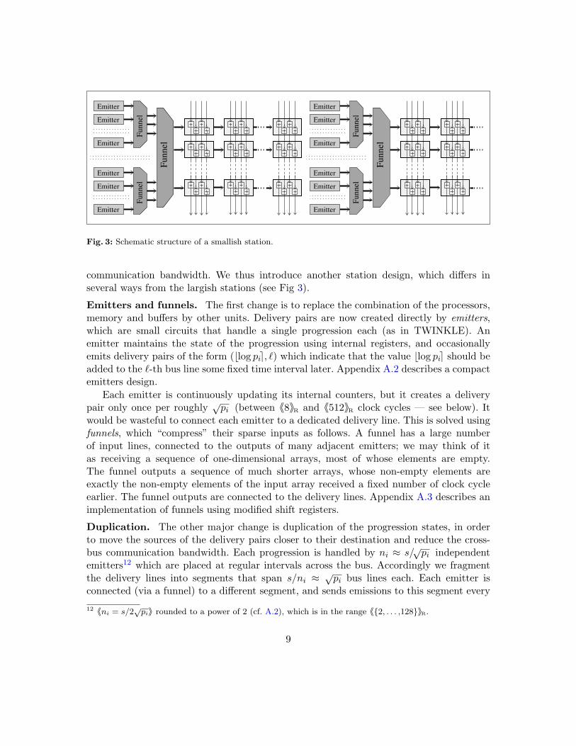
Fig. 3: Schematic structure of a smallish station.
communication bandwidth. We thus introduce another station design, which differs inseveral ways from the largish stations (see Fig 3).
Emitters and funnels. The first change is to replace the combination of the processors,memory and buffers by other units. Delivery pairs are now created directly by emitters,which are small circuits that handle a single progression each (as in TWINKLE). Anemitter maintains the state of the progression using internal registers, and occasionallyemits delivery pairs of the form (blog pie, `) which indicate that the value blog pie should beadded to the `-th bus line some fixed time interval later. Appendix A.2 describes a compactemitters design.
Each emitter is continuously updating its internal counters, but it creates a deliverypair only once per roughly
√pi (between 〈〈8〉〉R and 〈〈512〉〉R clock cycles — see below). It
would be wasteful to connect each emitter to a dedicated delivery line. This is solved usingfunnels, which “compress” their sparse inputs as follows. A funnel has a large numberof input lines, connected to the outputs of many adjacent emitters; we may think of itas receiving a sequence of one-dimensional arrays, most of whose elements are empty.The funnel outputs a sequence of much shorter arrays, whose non-empty elements areexactly the non-empty elements of the input array received a fixed number of clock cycleearlier. The funnel outputs are connected to the delivery lines. Appendix A.3 describes animplementation of funnels using modified shift registers.
Duplication. The other major change is duplication of the progression states, in orderto move the sources of the delivery pairs closer to their destination and reduce the cross-bus communication bandwidth. Each progression is handled by ni ≈ s/
√pi independent
emitters12 which are placed at regular intervals across the bus. Accordingly we fragmentthe delivery lines into segments that span s/ni ≈
√pi bus lines each. Each emitter is
connected (via a funnel) to a different segment, and sends emissions to this segment every
12 〈〈ni = s/2√
pi〉〉 rounded to a power of 2 (cf. A.2), which is in the range 〈〈2, . . . ,128〉〉R.
9

Emitt
er
Emitt
er
Emitt
er
Fig. 4: Schematic structure of a tiny station, for a single progression.
pi/sni ≈√
p clock cycles. As emissions reach their destination quicker, we can decreasethe total number of delivery lines. Also, there is a corresponding decrease in the emissionfrequency of any specific emitter, which allows us to handle pi close to (or even smaller than)s. Overall there are 〈〈501〉〉R delivery lines in the smallish stations, broken into segments ofvarious sizes.
Notes. Asymptotically the amortized circuit area per smallish progression is Θ( (s/√
pi +1) (log s+log pi) ). The term 1 is less innocuous than it appears — it hides a large constant(roughly the size of an emitter plus the amortized funnel size), which dominates the costfor large pi.
3.4 Tiny Primes
For very small primes, the amortized cost of the duplicated emitters, and in particularthe related funnels, becomes too high. On the other hand, such progressions cause severalemissions at every clock cycle, so it is less important to amortize the cost of delivery linesover several progressions. This leads to a third station design for the tiny primes 〈〈pi < 256〉〉.While there are few such progressions, their contributions are significant due to their verysmall periods.
Each tiny progression is handled independently, using a dedicated delivery line. Thedelivery line is partitioned into segments of size somewhat smaller than pi,13 and an emitteris placed at the input of each segment, without an intermediate funnel (see Fig 4). Theseemitters are a degenerate form of the ones used for smallish progressions (cf. A.2). Here wecannot interleave the adders in delivery cells as done in largish and smallish stations, butthe carry-save adders are smaller since they only (conditionally) add the small constantblog pie. Since the area occupied by each progression is dominated by the delivery lines, itis Θ(s) regardless of pi.
Some additional design considerations are discussed in Appendix A.
4 Cost estimates
Having outlined the design and specified the problem size, we next estimate the cost ofa hypothetical TWIRL device using today’s VLSI technology. The hardware parameters13 The segment length is the largest power of 2 smaller than pi (cf. A.2).
10

used are specified in Appendix B.1. While we tried to produce realistic figures, we stressthat these estimates are quite rough and rely on many approximations and assumptions.They should only be taken to indicate the order of magnitude of the true cost. We havenot done any detailed VLSI design, let alone actual implementation.
4.1 Cost of Sieving for 1024-bit Composites
We assume the following NFS parameters: BR = 3.5 · 109, BA = 2.6 · 1010, R = 1.1 · 1015,H ≈ 2.7 · 108 (cf. B.2). We use the cascaded sieves variant of Appendix A.6.
For the rational side we set sR = 4,096. One rational TWIRL device requires 15,960mm2
of silicon wafer area, or 1/4 of a 30cm silicon wafer. Of this, 76% is occupied by the largishprogressions (and specifically, 37% of the device is used for the DRAM banks), 21% is usedby the smallish progressions and the rest (3%) is used by the tiny progressions. For thealgebraic side we set sA = 32,768. One algebraic TWIRL device requires 65,900mm2 ofsilicon wafer area — a full wafer. Of this, 94% is occupied by the largish progressions (66%of the device is used for the DRAM banks) and 6% is used by the smallish progressions.Additional parameters of are mentioned throughout Section 3.
The devices are assembled in clusters that consist each of 8 rational TWIRLs and 1algebraic TWIRL, where each rational TWIRL has a unidirectional link to the algebraicTWIRL over which it transmits 12 bits per clock cycle. A cluster occupies three wafers,and handles a full sieve line in R/sA clock cycles, i.e., 33.4 seconds when clocked at 1GHz.The full sieving involves H sieve lines, which would require 194 years when using a singlecluster (after the 33% saving of Appendix A.5.) At a cost of $2.9M (assuming $5,000 perwafer), we can build 194 independent TWIRL clusters that, when run in parallel, wouldcomplete the sieving task within 1 year.
After accounting for the cost of packaging, power supply and cooling systems, addingthe cost of PCs for collecting the data and leaving a generous error margin,14 it appearsrealistic that all the sieving required for factoring 1024-bit integers can be completed within1 year by a device that cost $10M to manufacture. In addition to this per-device cost, therewould be an initial NRE cost on the order of $20M (for design, simulation, mask creation,etc.).
4.2 Implications for 1024-bit Composites
It has been often claimed that 1024-bit RSA keys are safe for the next 15 to 20 years, sinceboth NFS relation collection and the NFS matrix step would be unfeasible (e.g., [4,21] anda NIST guideline draft [18]). Our evaluation suggests that sieving can be achieved withinone year at a cost of $10M (plus a one-time cost of $20M), and recent works [16,8] indicatethat for our NFS parameters the matrix can also be performed at comparable costs.14 It is a common rule of thumb to estimate the total cost as twice the silicon cost; to be conservative, we
triple it.
11
With efficient custom hardware for both sieving and the matrix step, other subtasks inthe NFS algorithm may emerge as bottlenecks.15 Also, our estimates are hypothetical andrely on numerous approximations; the only way to learn the precise costs involved wouldbe to perform a factorization experiment.
Our results do not imply that breaking 1024-bit RSA is within reach of individualhackers. However, it is difficult to identify any specific issue that may prevent a sufficientlymotivated and well-funded organization from applying the Number Field Sieve to 1024-bit composites within the next few years. This should be taken into account by anyoneplanning to use a 1024-bit RSA key.
4.3 Cost of Sieving for 512-bits Composites
Since several hardware designs [19,15,10,7] were proposed for the sieving of 512-bit com-posites, it would be instructive to obtain cost estimates for TWIRL with the same problemparameters. We assume the same parameters as in [15,7]: BR = BA = 224 ≈ 1.7 · 107,R = 1.8 · 1010, 2H = 1.8 · 106. We set s = 1,024 and use the same cost estimation expres-sions that lead to the 1024-bit estimates.
A single TWIRL device would have a die size of about 800mm2, 56% of which areoccupied by largish progressions and most of the rest occupied by smallish progressions.It would process a sieve line in 0.018 seconds, and can complete the sieving task within6 hours.
For these NFS parameters TWINKLE would require 1.8 seconds per sieve line, theFPGA-based design of [10] would require about 10 seconds and the mesh-based designof [7] would require 0.36 seconds. To provide a fair comparison to TWINKLE and [7], weshould consider a single wafer full of TWIRL devices running in parallel. Since we can fit79 of them, the effective time per sieve line is 0.00022 seconds.
Thus, in factoring 512-bit composites the basic TWIRL design is about 1,600 timesmore cost effective than the best previously published design [7], and 8,100 times morecost effective than TWINKLE. Adjusting the NFS parameters to take advantage of thecascaded-sieves variant (cf. A.6) would further increase this gap. However, even when usingthe basic variant, a single wafer of TWIRLs can complete the sieving for 512-bit compositesin under 10 minutes.
4.4 Cost of Sieving for 768-bits Composites
We assume the following NFS parameters: BR = 1 · 108, BA = 1 · 109, R = 3.4 · 1013,H ≈ 8.9·106 (cf. B.2). We use the cascaded sieves variant of Appendix A.6, with sR = 1,024and sA = 4,096. For this choice, a rational sieve occupies 1,330mm2 and an algebraic sieveoccupies 4,430mm2. A cluster consisting of 4 rational sieves and one algebraic sieve can15 Note that for our choice of parameters, the cofactor factorization is cheaper than the sieving (cf. Ap-
pendix A.7).
12
process a sieve line in 8.3 seconds, and 6 independent clusters can fit on a single 30cmsilicon wafer.
Thus, a single wafer of TWIRL clusters can complete the sieving task within 95 days.This wafer would cost about $5,000 to manufacture — one tenth of the RSA-768 challengeprize [20].16
4.5 Larger composites
For largish progressions, the amortized cost per progression is Θ(s2(log s)/pi + log s +log pi) with small constants (cf. 3.2). For smallish progressions, the amortized cost isΘ( (s/
√pi + 1) (log s + log pi) ) with much larger constants (cf. 3.3). For a serial imple-
mentation (PC-based or TWINKLE), the cost per progression is clearly Ω(log pi). Thismeans that asymptotically we can choose s = Θ(
√B) to get a speed advantage of Θ(
√B)
over serial implementations, while maintaining the small constants. Indeed, we can keepincreasing s essentially for free until the area of the largish processors, buffers and deliverylines becomes comparable to the area occupied by the DRAM that holds the progressiontriplets.
For some range of input sizes, it may be beneficial to reduce the amount of DRAMused for largish progressions by storing only the prime pi, and computing the rest ofthe progression triplet values on-the-fly in the special-purpose processors (this requirescomputing the roots modulo pi of the relevant NFS polynomial).
If the device would exceed the capacity of a single silicon wafer, then as long as the busitself is narrower than a wafer, we can (with appropriate partitioning) keep each stationfully contained in some wafer; the wafers are connected in a serial chain, with the buspassing through all of them.
5 Conclusion
We have presented a new design for a custom-built sieving device. The device consistsof a thick pipeline that carries sieve locations through thrilling adventures, where theyexperience the addition of progression contributions in myriad different ways that areoptimized for various scales of progression periods. In factoring 512-bit integers, the newdevice is 1,600 times faster than best previously published designs. For 1024-bit compositesand appropriate choice of NFS parameters, the new device can complete the sieving taskwithin 1 year at a cost of $10M, thereby raising some concerns about the security of 1024-bitRSA keys.
Acknowledgments. This work was inspired by Daniel J. Bernstein’s insightful work onthe NFS matrix step, and its adaptation to sieving by Willi Geiselmann and Rainer Stein-wandt. We thank the latter for interesting discussions of their design and for suggesting an16 Needless to say, this disregards an initial cost of about $20M. This initial cost can be significantly reduced
by using older technology, such as 0.25µm process, in exchange for some decrease in sieving throughput.
13

improvement to ours. We are indebted to Arjen K. Lenstra for many insightful discussions,and to Robert D. Silverman, Andrew “bunnie” Huang and Michael Szydlo for valuablecomments and suggestions. Early versions of [14] and the polynomial selection programsof Jens Franke and Thorsten Kleinjung were indispensable in obtaining refined estimatesfor the NFS parameters.
References
1. F. Bahr, J. Franke, T. Kleinjung, M. Lochter, M. Bohm, RSA-160, e-mail announcement, Apr. 2003,http://www.loria.fr/~zimmerma/records/rsa160
2. Daniel J. Bernstein, How to find small factors of integers, manuscript, 2000,http://cr.yp.to/papers.html
3. Daniel J. Bernstein, Circuits for integer factorization: a proposal, manuscript, 2001,http://cr.yp.to/papers.html
4. Richard P. Brent, Recent progress and prospects for integer factorisation algorithms, proc. COCOON2000, LNCS 1858 3–22, Springer-Verlag, 2000
5. S. Cavallar, B. Dodson, A.K. Lenstra, W. Lioen, P.L. Montgomery, B. Murphy, H.J.J. te Riele, et al.,Factorization of a 512-bit RSA modulus, proc. Eurocrypt 2000, LNCS 1807 1–17, Springer-Verlag, 2000
6. Don Coppersmith, Modifications to the number field sieve, Journal of Cryptology 6 169–180, 19937. Willi Geiselmann, Rainer Steinwandt, A dedicated sieving hardware, proc. PKC 2003, LNCS 2567
254–266, Springer-Verlag, 20028. Willi Geiselmann, Rainer Steinwandt, Hardware to solve sparse systems of linear equations over GF(2),
proc. CHES 2003, LNCS, Springer-Verlag, to be published.9. International Technology Roadmap for Semiconductors 2001, http://public.itrs.net/
10. Hea Joung Kim, William H. Magione-Smith, Factoring large numbers with programmable hardware,proc. FPGA 2000, ACM, 2000
11. Robert Lambert, Computational aspects of discrete logarithms, Ph.D. Thesis, University of Waterloo,1996
12. Arjen K. Lenstra, H.W. Lenstra, Jr., (eds.), The development of the number field sieve, Lecture Notesin Math. 1554, Springer-Verlag, 1993
13. Arjen K. Lenstra, Bruce Dodson, NFS with four large primes: an explosive experiment, proc. Crypto’95, LNCS 963 372–385, Springer-Verlag, 1995
14. Arjen K. Lenstra, Bruce Dodson, James Hughes, W. Kortsmit, Paul Leyland, Factoring estimates for1024-bit RSA modulus, to be published.
15. Arjen K. Lenstra, Adi Shamir, Analysis and Optimization of the TWINKLE Factoring Device, proc.Eurocrypt 2002, LNCS 1807 35–52, Springer-Verlag, 2000
16. Arjen K. Lenstra, Adi Shamir, Jim Tomlinson, Eran Tromer, Analysis of Bernstein’s factorizationcircuit, proc. Asiacrypt 2002, LNCS 2501 1–26, Springer-Verlag, 2002
17. Brian Murphy, Polynomial selection for the number field sieve integer factorization algorithm, Ph. D.thesis, Australian National University, 1999
18. National Institute of Standards and Technology, Key management guidelines, Part 1: General guidance(draft), Jan. 2003, http://csrc.nist.gov/CryptoToolkit/tkkeymgmt.html
19. Adi Shamir, Factoring large numbers with the TWINKLE device (extended abstract), proc. CHES’99,LNCS 1717 2–12, Springer-Verlag, 1999
20. RSA Security, The new RSA factoring challenge, web page, Jan. 2003,http://www.rsasecurity.com/rsalabs/challenges/factoring/
21. Robert D. Silverman, A cost-based security analysis of symmetric and asymmetric key lengths, Bulletin13, RSA Security, 2000,http://www.rsasecurity.com/rsalabs/bulletins/bulletin13.html
22. Web page for this paper, http://www.wisdom.weizmann.ac.il/~tromer/twirl
14

A Additional Design Considerations
A.1 Delivery Lines
The delivery lines are used by all station types to carry delivery pairs from their source(buffer, funnel or emitter) to their destination bus line. Their basic structure is describedin Section 3.2. We now describe methods for implementing them efficiently.Interleaving. Most of the time the cells in a delivery line act as shift registers, and theiradders are unused. Thus, we can reduce the cost of adders and registers by interleaving. Weuse larger delivery cells that span r 〈〈= 4〉〉R adjacent bus lines, and contain an adder justfor the q-th line among these, with q fixed throughout the delivery line and incrementedcyclically in the subsequent delivery lines. As a bonus, we now put every r adjacent deliverylines in a single bus pipeline stage, so that it contains one adder per bus line. This reducingthe number of bus pipelining registers by a factor of r throughout the largish stations.
Since the emission pairs traverse the delivery lines at a rate of r lines per clock cycle,we need to skew the space-time assignment of sieve locations so that as distance from thebuffer to the bus line increases, the “age” ba/sc of the sieve locations decreases. Moreexplicitly: at time t, sieve location a is handled by the b(a mod s)/rc-th cell17 of one of ther delivery lines at stage t− ba/src − b(a mod s)/rc of the bus pipeline, if it exists.
In the largish stations, the buffer is entrusted with the role of sending delivery pairs todelivery lines that have an adder at the appropriate bus line; an improvement by a factorof 2 is achieved by placing the buffers at the middle of the bus, with the two halves of eachdelivery line directed outwards from the buffer. In the smallish and tiny stations we do notuse interleaving.
Note that whenever we place pipelining registers on the bus, we must delay all down-stream delivery lines connected to this buffer by a clock cycle. This can be done by addingpipeline stages at the beginning of these delivery lines.Carry-save adders. Logically, each bus line carries a log2T 〈〈= 10〉〉-bit integer. These areencoded by a redundant representation, as a pair of log2T -bit integers whose sum equalsthe sum of the blog pie contributions so far. The additions at the delivery cells are doneusing carry-save adders, which have inputs a,b,c and whose output is a representation ofthe sum of their inputs in the form of a pair e,f such that e + f = a + b + c. Carry-saveadders are very compact and support a high clock rate, since they do not propagate carriesacross more than one bit position. Their main disadvantage is that it is inconvenient toperform other operations directly on the redundant representation, but in our applicationwe only need to perform a long sequence of additions followed by a single comparison atthe end. The extra bus wires due to the redundant representation can be accommodatedusing multiple metal layers of the silicon wafer.18
17 After the change made in Appendix A.2 this becomes brev(a mod s)/rc, where rev(·) denotes bit-reversalof log2s-bit numbers and s,r are powers of 2.
18 Should this prove problematic, we can use the standard integer representation with carry-lookaheadadders, at some cost in circuit area and clock rate.
15

To prevent wrap-around due to overflow when the sum of contributions is much largerthan T , we slightly alter the carry-save adders by making their most significant bits“sticky”: once the MSBs of both values in the redundant representation become 1 (inwhich case the sum is at least T ), further additions do not switch them back to 0.
A.2 Implementation of Emitters
The designs of smallish and tiny progressions (cf. 3.3, 3.4) included emitter elements. Anemitter handles a single progression Pi, and its role is to emit the delivery pairs (blog pie, `)addressed to a certain group G of adjacent lines, ` ∈ G. This subsection describes ourproposed emitter implementation. For context, we first describe some less efficient designs.
Straightforward implementations. One simple implementation would be to keep adlog2pie-bit register and increment it by s modulo pi every clock cycle. Whenever a wrap-around occurs (i.e., this progression causes an emission), compute ` and check if ` ∈ G.Since the register must be updated within one clock cycle, this requires an expensivecarry-lookahead adder. Moreover, if s and |G| are chosen arbitrarily then calculating ` andtesting whether ` ∈ G may also be expensive. Choosing s, |G| as power of 2 reduces thecosts somewhat.
A different approach would be to keep a counter that counts down the time to the nextemission, as in [19], and another register that keeps track of `. This has two variants. Ifthe countdown is to the next emission of this triplet regardless of its destination bus line,then these events would occur very often and again require low-latency circuitry (also, thiscannot handle pi < s). If the countdown is to the next emission into G, we encounter thefollowing problem: for any set G of bus lines corresponding to adjacent residues modulo s,the intervals at which Pi has emissions into G are irregular, and would require expensivecircuitry to compute.
Line address bit reversal. To solve the last problem described above and use thesecond countdown-based approach, we note the following: the assignment of sieve locationsto bus lines (within a clock cycle) can be done arbitrarily, but the partition of wires intogroups G should be done according to physical proximity. Thus, we use the followingtrick. Choose s = 2α and |G| = 2βi ≈ √pi for some integers α 〈〈= 12〉〉R〈〈= 15〉〉A and βi. Theresidues modulo s are assigned to bus lines with bit-reversed indices; that is, sieve locationscongruent to w modulo s are handled by the bus line at physical location rev(w), where
w =α−1∑i=0
ci2i , rev(w) =α−1∑i=0
cα−1−i2i for some c0, . . . ,cα−1 ∈ 0,1
The j-th emitter of the progression Pi, j ∈ 0, . . . ,2α−βi, is in charge of the j-th group of2βi bus lines. The advantage of this choice is the following.
16

Lemma 1. For any fixed progression with pi > 2, the emissions destined to any fixed groupoccur at regular time intervals of Ti = b2−βipic, up to an occasional delay of one clock cycledue to modulo s effects.
Proof. Emissions into the j-th group correspond to sieve locations a ∈ Pi that fulfillbrev(a mod s)/2βic = j, which is equivalent to a ≡ cj (mod 2α−βi) for some cj . Since a ∈ Pi
means a ≡ ri (mod pi) and pi is coprime to 2α−βi , by the Chinese Remainder Theorem weget that the set of such sieve locations is exactly Pi,j ≡ a : a ≡ ci,j (mod 2α−βipi) for someci,j . Thus, a pair of consecutive a1,a2 ∈ Pi,j fulfill a2 − a1 = 2α−βipi. The time differencebetween the corresponding emissions is ∆ = ba2/sc − ba1/sc. If (a2 mod s) > (a1 mod s)then ∆ = b(a2 − a1)/sc = b2α−βipi/sc = Ti. Otherwise, ∆ = d(a2 − a1)/se = Ti + 1.
Note that Ti ≈√
pi , by the choice of βi.
Emitter structure. In the smallish stations, each emitter consists of two counters, asfollows.
– Counter A operates modulo Ti = b2−βipic (typically 〈〈7〉〉R〈〈5〉〉A bits), and keeps track ofthe time until the next emission of this emitter. It is decremented by 1 (nearly) everyclock cycle.
– Counter B operates modulo 2βi (typically 〈〈10〉〉R〈〈15〉〉A bits). It keeps track of the βi
most significant bits of the residue class modulo s of the sieve location correspondingto the next emission. It is incremented by 2α−βipi mod 2βi whenever Counter A wrapsaround. Whenever Counter B wraps around, Counter A is suspended for one clock cycle(this corrects for the modulo s effect).
A delivery pair (blog pie, `) is emitted when Counter A wraps around, where blog pie is fixedfor each emitter. The target bus line ` gets βi of its bits from Counter B. The α − βi
least significant bits of ` are fixed for this emitter, and they are also fixed throughout therelevant segment of the delivery line so there is no need to transmit them explicitly.
The physical location of the emitter is near (or underneath) the group of bus linesto which it is attached. The counters and constants need to be set appropriately duringdevice initialization. Note that if the device is custom-built for a specific factorization taskthen the circuit size can be reduced by hard-wiring many of these values19. The combinedlength of the counters is roughly log2 pi bits, and with appropriate adjustments they canbe implemented using compact ripple adders20 as in [15].
Emitters for tiny progressions. For tiny stations, we use a very similar design. Thebus lines are again assigned to residues modulo s in bit-reversed order (indeed, it would bequite expensive to reorder them). This time we choose βi such that |G| = 2βi is the largestpower of 2 that is smaller than pi. This fixes Ti = 1, i.e., an emission occurs every one or19 For sieving the rational side of NFS, it suffices to fix the smoothness bounds. Similarly for the prepro-
cessing stage of Coppersmith’s Factorization Factory [6] .20 This requires insertion of small delays and tweaking the constant values.
17

two clock cycles. The emitter circuitry is identical to the above; note that Counter A hasbecome zero-sized (i.e., a wire), which leaves a single counter of size βi ≈ log2pi bits.
A.3 Implementation of Funnels
The smallish stations use funnels to compact the sparse outputs of emitters before theyare passed to delivery lines (cf. 3.3). We implement these funnels as follows.
An n-to-m funnel (nm) consists of a matrix of n columns and m rows, where eachcell contains registers for storing a single progression triplet. At every clock cycle inputs arefed directly into the top row, one input per column, scheduled such that the i-th elementof the t-th input array is inserted into the i-th column at time t + i. At each clock cycle,all values are shifted horizontally one column to the right. Also, each value is shifted onerow down if this would not overwrite another value. The t-th output array is read off therightmost column at time t + n.
For any m < n there is some probability of “overflow” (i.e., insertion of input value intoa full column). Assuming that each input is non-empty with probability ν independentlyof the others (ν ≈ 1/
√pi ; cf. 3.3), the probability that a non-empty input will be lost due
to overflow is:n∑
k=m+1
(n
k
)νk(1− ν)n−k(k −m)/k
We use funnels with 〈〈m = 5〉〉R rows and 〈〈n ≈ 1/ν〉〉R columns. For this choice and withinthe range of smallish progressions, the above failure probability is less than 0.00011. Thiscertainly suffices for our application.
The above funnels have a suboptimal compression ratio n/m 〈〈≈ 1/5ν〉〉R, i.e., the prob-ability ν ′ 〈〈≈ 1/5〉〉R of a funnel output value being non-empty is still rather low. We thusfeed these output into a second-level funnel 〈〈with m′ = 35, n′ = 14〉〉R, whose overflowprobability is less than 0.00016, and whose cost is amortized over many progressions. Theoutput of the second-level funnel is fed into the delivery lines. The combined compressionratio of the two funnel levels is suboptimal by a factor of 5 · 14/34 = 2, so the number ofdelivery lines is twice the naive optimum. We do not interleave the adders in the deliv-ery lines as done for largish stations (cf. A.1), in order to avoid the overhead of directingdelivery pairs to an appropriate delivery line.21
A.4 Initialization
The device initialization consists of loading the progression states and initial counter valuesinto all stations, and loading instructions into the bus bypass re-routing switches (aftermapping out the defects).
21 Still, the number of adders can be reduced by attaching a single adder to several bus lines using multi-plexers. This may impact the clock rate.
18

The progressions differ between sieving runs, but reloading the device would requiresignificant time (in [19] this became a bottleneck). We can avoid this by noting, as in [7],that the instances of sieving problem that occur in the NFS are strongly related, andall that is needed is to increase each ri value by some constant value ri after each run.The ri values can be stored compactly in DRAM using log2pi bits per progression (thisis included in our cost estimates) and the addition can be done efficiently using on-waferspecial-purpose processors. Since the interval R/s between updates is very large, we don’tneed to dedicate significant resources to performing the update quickly. For lattice sievingthe situation is somewhat different (cf. A.8).
A.5 Eliminating Sieve Locations
In the NFS relation collection, we are only interesting in sieve locations a on the b-th sieveline for which gcd(a′,b) = 1 where a′ = a−R/2, as other locations yield duplicate relations.The latter are eliminated by the candidate testing, but the sieving work can be reducedby avoiding sieve locations with c |a′,b for very small c. All software-based sievers considerthe case 2 |a′,b — this eliminates 25% of the sieve locations. In TWIRL we do the same:first we sieve normally over all the odd lines, b ≡ 1(mod 2). Then we sieve over the evenlines, and consider only odd a′ values; since a progression with pi > 2 hits every pi-th oddsieve location, the only change required is in the initial values loaded into the memoriesand counters. Sieving of these odd lines takes half the time compared to even lines.
We also consider the case 3 |a′,b, similarly to the above. Combining the two, we get fourtypes of sieve runs: full-, half-, third- and sixth-length runs, for b mod 6 in 1,5, 2,4,3 and 0 respectively. Overall, we get a 33% time reduction, essentially for free. It isnot worthwhile to consider c |a′,b for c > 3.
A.6 Cascading the Sieves
Recall that the instances of the sieving problem come in pairs of rational and algebraicsieves, and we are interested in the a values that passed both sieves (cf. 2.1). However,the situation is not symmetric: BR 〈〈2.6 · 1010〉〉A is much larger than BR 〈〈= 3.5 · 109〉〉R.22
Therefore the cost of the algebraic sieves would dominate the total cost when s is chosenoptimally for each sieve type. Moreover, for 1024-bit composites and the parameters weconsider (cf. Appendix B), we cannot make the algebraic-side s as large as we wish becausethis would exceed the capacity of a single silicon wafer. The following shows a way toaddress this.
Let sR and sA denote the s values of the rational and algebraic sieves respectively. Thereason we cannot increase sA and gain further “free” parallelism is that the bus becomesunmanageably wide and the delivery lines become numerous and long (their cost is Θ(s2)).
22 BA and BR are chosen as to produce a sufficient probability of semi-smoothness for the values over whichwe are (implicitly) sieving: circa 〈〈10101〉〉A vs. circa 〈〈1064〉〉R.
19

However, the bus is designed to sieve sA sieve locations per pipeline stage. If we first executethe rational sieve then most of these sieve locations can be ruled out in advance: all but asmall fraction 〈〈1.7 · 10−4〉〉 of the sieve locations do not pass the threshold in the rationalsieve,23 and thus cannot form candidates regardless of their algebraic-side quality.
Accordingly, we make the following change in the design of algebraic sieves. Insteadof a wide bus consisting of sA lines that are permanently assigned to residues modulo sA,we use a much narrower bus consisting of only u 〈〈= 32〉〉A lines, where each line containsa pair (C,L). L = (a mod sA) identifies the sieve location, and C is the sum of blog piecontributions to a so far. The sieve locations are still scanned in a pipelined manner at arate of sA locations per clock cycle, and all delivery pairs are generated as before at therespective units.
The delivery lines are different: instead of being long and “dumb”, they are now shortand “smart”. When a delivery pair (blog pie, `) is generated, ` is compared to L for each ofthe u lines (at the respective pipeline stage) in a single clock cycle. If a match is found,blog pie is added to the C of that line. Otherwise (i.e., in the overwhelming majority ofcases), the delivery pair is discarded.
At the head of the bus, we input pairs (0, a mod sA) for the sieve locations a thatpassed the rational sieve. To achieve this we wire the outputs of rational sieves to inputsof algebraic sieves, and operate them in a synchronized manner (with the necessary phaseshift). Due to the mismatch in s values, we connect sA/sB rational sieves to each algebraicsieves. Each such cluster of sA/sB + 1 sieving devices is jointly applied to one single sieveline at a time, in a synchronized manner. To divide the work between the multiple rationalsieves, we use interleaving of sieve locations (similarly to the bit-reversal technique of A.2).Each rational-to-algebraic connection transmits at most one value of size log2sR 〈〈12〉〉 bitsper clock cycle (appropriate buffering is used to average away congestions).
This change greatly reduces the circuit area occupied by the bus wiring and deliverylines; for our choice of parameters, it becomes insignificant. Also, there is no longer needto duplicate emitters for smallish progressions (except when pi < s). This allows us to usea large s 〈〈= 32,768〉〉A for the algebraic sieves, thereby reducing their cost to less than thatof the rational sieve (cf. 4.1). Moreover, it lets us further increase BA with little effect oncost, which (due to tradeoffs in the NFS parameter choice) reduces H and R.
A.7 Testing Candidates
Having computed approximations of the sum of logarithms g(a) for each sieve location a,we need to identify the resulting candidates, compute the corresponding sets i : a ∈ Pi,and perform some additional tests (cf. 2.1). These are implemented as follows.
Identifying candidates. In each TWIRL device, at the end of the bus (i.e., downstreamfor all stations) we place an array of comparators, one per bus line, that identify a values
23 Before the cofactor factorization. Slightly more when blog pie rounding is considered.
20

for which g(a) > T . In the basic TWIRL design, we operate a pair of sieves (one rationaland one algebraic) in unison: at each clock cycle, the sets of bus lines that passed thecomparator threshold are communicated between the two devices, and their intersection(i.e., the candidates) are identified. In the cascaded sieves variant, only sieve locationsthat passed the threshold on the rational TWIRL are further processed by the algebraicTWIRL, and thus the candidates are exactly those sieve locations that passed the thresholdin the algebraic TWIRL. The fraction of sieve locations that constitute candidates is verysmall 〈〈2 · 10−11〉〉.
Finding the corresponding progressions. For each candidate we need to compute theset i : a ∈ Pi, separately for the rational and algebraic sieves. From the context in theNFS algorithm it follows that the elements of this set for which pi is relatively small can befound easily.24 It thus appears sufficient to find the subset i : a ∈ Pi , pi is largish, whichis accomplished by having largish stations remember the pi values of recent progressionsand report them upon request.
To implement this, we add two dedicated pipelined channels passing through all theprocessors in the largish stations. The lines channel, of width log2s bits, goes upstream(i.e., opposite to the flow of values in the bus) from the threshold comparators. The divisorschannel, of width log2B bits, goes downstream. Both have a pipeline register after eachprocessor, and both end up as outputs of the TWIRL device. To each largish processor weattach a diary, which is a cyclic list of log2B-bit values. Every clock cycle, the processorwrites a value to its diary: if the processor inserted an emission triplet (blog pie, `i, τi) intothe buffer at this clock cycle, it writes the triple (pi, `i, τi) to the diary; otherwise it writesa designated null value. When a candidate is identified at some bus line `, the value `is sent upstream through the lines channel. Whenever a processor sees an ` value on thelines channel, it inspects its diaries to see whether it made an emission that was added tobus line ` exactly z clock cycles ago, where z is the distance (in pipeline stages) from theprocessor’s output into the buffer, through the bus and threshold comparators and backto the processor through the lines channel. This inspection is done by searching the 〈〈64〉〉diary entries preceeding the one written z clock cycles ago for a non-null value (pi, `i) with`i = `. If such a diary entry is found, the processor transmits pi downstream via the divisorschannel (with retry in case of collision). The probability of intermingling data belonging todifferent candidates is negligible, and even then we can recover (by appropriate divisibilitytests).
In the cascaded sieves variant, the algebraic sieve records to diaries only those contri-butions that were not discarded at the delivery lines. The rational diaries are rather large(〈〈13,530〉〉R entries) since they need to keep their entries a long time — the latency z in-cludes passing through (at worst) all rational bus pipeline stages, all algebraic bus pipelinestages and then going upstream through all rational stations. However, these diaries can
24 Namely, by finding the small factors of Fj(a−R,b) where Fj is the relevant NFS polynomial and b is theline being sieved.
21
be implemented very efficiently as DRAM banks of a degenerate form with a fixed cyclicaccess order (similarly to the memory banks of the largish stations).Testing candidates. Given the above information, the candidates have to be furtherprocessed to account for the various approximations and errors in sieving, and to account forthe NFS “large primes” (cf. 2.1). The first steps (computing the values of the polynomials,dividing out small factors and the diary reports, and testing size and primality of remainingcofactors) can be effectively handled by special-purpose processors and pipelines, which aresimilar to the division pipeline of [7, Section 4] except that here we have far fewer candidates(cf. C).Cofactor factorization. The candidates that survived the above steps (and whose co-factors were not prime or sufficiently small) undergo cofactor factorization. This involvesfactorization of one (and seldom two) integers of size at most 〈〈1·1024〉〉. Less than 〈〈2·10−11〉〉of the sieve locations reach this stage (this takes blog pie rounding errors into consideration),and a modern general-purpose processor can handle each in less than 0.05 seconds. Thus,using dedicated hardware this can be performed at a small fraction of the cost of sieving.Also, certain algorithmic improvements may be applicable [2].
A.8 Lattice Sieving
The above is motivated by NFS line sieving, which has very large sieve line length R.Lattice sieving (i.e., ”special-q”) involves fewer sieving locations. However, lattice sievinghas very short sieving lines (8192 in [5]), so the natural mapping to the lattice problem asdefined here (i.e., lattice sieving by lines) leads to values of R that are too small.
We can adapt TWIRL to efficient lattice sieving as follows. Choose s equal to thewidth of the lattice sieving region (they are of comparable magnitude); a full lattice line ishandled at each clock cycle, and R is the total number of points in the sieved lattice block.The definition (pi,ri) is different in this case — they are now related to the vectors used inlattice sieving by vectors (before they are lattice-reduced). The handling of modulo s wrap-around of progressions is now somewhat more complicated, and the emission calculationlogic in all station types needs to be adapted. Note that the largish processors are essentiallyperforming lattice sieving by vectors, as they are “throwing” values far into the “future”,not to be seen again until their next emission event.
Re-initialization is needed only when the special-q lattices are changed (every 8192·5000sieve locations in [5]), but is more expensive. Given the benefits of lattice sieving, it may beadvantageous to use faster (but larger) re-initialization circuits and to increase the sievingregions (despite the lower yield); this requires further exploration.
A.9 Fault Tolerance
Due to its size, each TWIRL device is likely to have multiple local defects caused byimperfections in the VLSI process. To increase the yield of good devices, we make thefollowing adaptations.
22

If any component of a station is defective, we simply avoid using this station. Usinga small number of spare stations of each type (with their constants stored in reloadablelatches), we can handle the corresponding progressions.
Since our device uses an addition pipeline, it is highly sensitive to faults in the bus linesor associated adders. To handle these, we can add a small number of spare line segmentsalong the bus, and logically re-route portions of bus lines through the spare segments inorder to bypass local faults. In this case, the special-purpose processors in largish stationscan easily change the bus destination addresses (i.e., ` value of emission triplets) to accountfor re-routing. For smallish and tiny stations it appears harder to account for re-routing, sowe just give up adding the corresponding blog pie values; we may partially compensate byadding a small constant value to the re-routed bus lines. Since the sieving step is intendedonly as a fairly crude (though highly effective) filter, a few false-positives or false-negativesare acceptable.
B Parameters for Cost Estimates
B.1 Hardware
The hardware parameters used are those given in [16] (which are consistent with [9]):standard 30cm silicon wafers with 0.13µm process technology, at an assumed cost of $5,000per wafer. For 1024-bit and 768-bit composites we will use DRAM-type wafers, which weassume to have a transistor density of 2.8 µm2 per transistor (averaged over the logic area)and DRAM density of 0.2µm2 per bit (averaged over the area of DRAM banks). For 512-bitcomposites we will use logic-type wafers, with transistor density of 2.38µm2 per transistorand DRAM density of 0.7µm2 per bit. The clock rate is 1GHz clock rate, which appearsrealistic with judicious pipelining of the processors.
We have derived rough estimates for all major components of the design; this requiredadditional analysis, assumptions and simulation of the algorithms. Here are some highlights,for 1024-bit composites with the choice of parameters specified throughout Section 3. Atypical largish special-purpose processor is assumed to require the area of 〈〈96,400〉〉R logic-density transistors (including the amortized buffer area and the small amount of cachememory, about 〈〈14Kbit〉〉R, that is independent of pi). A typical emitter is assumed torequire 〈〈2,037〉〉R transistors in a smallish station (including the amortized costs of funnels),and 〈〈522〉〉R in a tiny station. Delivery cells are assumed to require 〈〈530〉〉R transistors withinterleaving (i.e., in largish stations) and 〈〈1220〉〉R without interleaving (i.e., in smallishand tiny stations). We assume that the memory system of Section 3.2 requires 〈〈2.5〉〉 timesmore area per useful bit than standard DRAM, due to the required slack and and area ofthe cache. We assume that bus wires don’t require wafer area apart from their pipeliningregisters, due to the availability of multiple metal layers. We take the cross-bus density ofbus wires to be 〈〈0.5〉〉 bits per µm, possibly achieved by using multiple metal layers.
Note that since the device contains many interconnected units of non-uniform size,designing an efficient layout (which we have not done) is a non-trivial task. However, the
23

Table 1: Sieving parameters.
Parameter Meaning 1024-bit 768-bit 512-bit
R Width of sieve line 1.1 · 1015 3.4 · 1013 1.8 · 1010
H Number of sieve lines 2.7 · 108 8.9 · 106 9.0 · 105
BR Rational smoothness bound 3.5 · 109 1 · 108 1.7 · 107
BA Algebraic smoothness bound 2.6 · 1010 1 · 109 1.7 · 107
number of different unit types is very small compared to designs that are commonly handledby the VLSI industry, and there is considerable room for variations. The mostly systolicdesign also enables the creation devices larger than the reticle size, using multiple steps ofa single (or very few) mask set.
Using a fault-tolerant design (cf. A.9), the yield can made very high and functional test-ing can be done at a low cost after assembly. Also, the acceptable probability of undetectederrors is much higher than that of most VLSI designs.
B.2 Sieving Parameters
To predict the cost of sieving, we need to estimate the relevant NFS parameters (R, H, BR,BA). The values we used are summarized in Table 1. The parameters for 512-bit compositesare the same as those postulated for TWINKLE [15] and appear conservative compared toactual experiments [5].
To obtain reasonably accurate predictions for larger composites, we followed the ap-proach of [14]; namely, we generated concrete pairs of NFS polynomials for the RSA-1024and RSA-768 challenge composites [20] and estimated their relations yield. The search forNFS polynomials was done using programs written by Jens Franke and Thorsten Klein-jung (with minor adaptations). For our 1024-bit estimates we picked the following pair ofpolynomials, which have a common integer root modulo the RSA-1024 composite:
f(x) = 1719304894236345143401011418080x5
− 6991973488866605861074074186043634471x4
+ 27086030483569532894050974257851346649521314x3
+ 46937584052668574502886791835536552277410242359042x2
− 101070294842572111371781458850696845877706899545394501384x
− 22666915939490940578617524677045371189128909899716560398434136
g(x) = 93877230837026306984571367477027x
− 37934895496425027513691045755639637174211483324451628365
Subsequent analysis of relations yield was done by integrating the relevant smoothnessprobability functions [11] over the sieving region. Successful factorization requires findingsufficiently many cycles among the relations, and for two large primes per side (as weassumed) it is currently unknown how to predict the number of cycles from the numberof relations, but we verified that the numbers appear “reasonable” compared to current
24

experience with smaller composites. The 768-bit parameters were derived similarly. Moredetails are available in a dedicated web page [22] and in [14].
Note that finding better polynomials will reduce the cost of sieving. Indeed, our algebraic-side polynomial is of degree 5 (due to a limitation of the programs we used), while there aretheoretical and empirical reasons to believe that polynomials of somewhat higher degreecan have significantly higher yield.
C Relation to Previous Works
TWINKLE. As is evident from the presentation, the new device shares with TWINKLEthe property of time-space reversal compared to traditional sieving. TWIRL is obviouslyfaster than TWINKLE, as two have comparable clock rates but the latter checks one sievelocation per clock cycle whereas the former checks thousands. None the less, TWIRL issmaller than TWINKLE — this is due to the efficient parallelization and the use of compactDRAM storage for the largish progressions (it so happens that DRAM cannot be efficientlyimplemented on GaAs wafers, which are used by TWINKLE). We may consider usingTWINKLE-like optical analog adders instead of electronic adder pipelines, but constructinga separate optical adder for each residue class modulo s would entail practical difficulties,and does not appear worthwhile as there are far fewer values to sum.
FPGA-based serial sieving. Kim and Mangione-Smith [10] describe a sieving deviceusing off-the-shelf parts that may be only 6 times slower than TWINKLE. It uses classicalsieving, without time-memory reversal. The speedup follows from increased memory band-width – there are several FPGA chips and each is connected to multiple SRAM chips. Aspresented this implementation does not rival the speed or cost of TWIRL. Moreover, sinceit is tied to a specific hardware platform, it is unclear how it scales to larger parallelismand larger sieving problems.
Low-memory sieving circuits. Bernstein [3] proposes to completely replace sievingby memory-efficient smoothness testing methods, such as the Elliptic Curve Method offactorization. This reduces the asymptotic time× space cost of the matrix step from y3+o(1)
to y2+o(1), where y is subexponential in the length of the integer being factored and dependson the choice of NFS parameters. By comparison, TWIRL has a throughput cost of y2.5+o(1),because the speedup factor grows as the square root of the number of progressions (cf. 4.5).However, these asymptotic figures hide significant factors; based on current experience, for1024-bit composites it appears unlikely that memory-efficient smoothness testing wouldrival the practical performance of traditional sieving, let alone that of TWIRL, in spite ofits superior asymptotic complexity.
Mesh-based sieving. While [3] deals primarily with the NFS matrix step, it does men-tion “sieving via Schimmler’s algorithm” and notes that its cost would be L2.5+o(1) (likeTWIRL’s). Geiselmann and Steinwandt [7] follow this approach and give a detailed de-sign for a mesh-based sieving circuit. Compared to previous sieving devices, both [7] and
25

TWIRL achieve a speedup factor of Θ(√
B).25 However, there are significant differences inscalability and cost: TWIRL is 1,600 times more efficient for 512-bit composites, and evermore so for bigger composites or when using the cascaded sieves variant (cf. 4.3, A.6).
One reason is as follows. The mesh-based sorting of [7] is effective in terms of latency,which is why it was appropriate for the Bernstein’s matrix-step device [3] where the inputto each invocation depended on the output of the previous one. However, for sieving wecare only about throughput. Disregarding latency leads to smaller circuits and higher clockrates. For example, TWIRL’s delivery lines perform trivial one-dimensional unidirectionalrouting of values of size 〈〈12 + 10〉〉R bits, as opposed to complicated two-dimensional meshsorting of progression states of size 〈〈2 · 31.7〉〉R.26 For the algebraic sieves the situation iseven more extreme (cf. A.6).
In the design of [7], the state of each progression is duplicated dΘ(B/pi)e times (com-pared to dΘ(
√B/pi)e in TWIRL) or handled by other means; this greatly increases the
cost. For the primary set of design parameters suggested in [7] for factoring 512-bit num-bers, 75% of the mesh is occupied by duplicated values even though all primes smaller than217 are handled by other means: a separate division pipeline that tests potential candidatesidentified by the mesh, using over 12,000 expensive integer division units. Moreover, thisassumes that the sums of blog pie contributions from the progressions with pi > 217 aresufficiently correlated with smoothness under all progressions; it is unclear whether thisassumption scales.
TWIRL’s handling of largish primes using DRAM storage greatly reduces the size ofthe circuit when implemented using current VLSI technology (90 DRAM bits vs. about2500 transistors in [7]).
If the device must span multiple wafers, the inter-wafer bandwidth requirements of ourdesign are much lower than that of [7] (as long as the bus is narrower than a wafer), andthere is no algorithmic difficulty in handling the long latency of cross-wafer lines. Moreover,connecting wafers in a chain may be easier than connecting them in a 2D mesh, especiallyin regard to cooling and faults.
25 Possibly less for [7] — an asymptotic analysis is lacking, especially in regard to the handling of smallprimes.
26 The authors of [7] have suggested (in private communication) a variant of their device that routes emis-sions instead of sorting states, analogously to [16]. Still, mesh routing is more expensive than pipelineddelivery lines.
26