“f1 WHW
49
US 20030111682A1 (12) Patent Application Publication (10) Pub. No.: US 2003/0111682 A1 (19) United States Tanaka et al. (43) Pub. Date: Jun. 19, 2003 (54) NONVOLATILE MEMORY AND PROCESSING SYSTEM (75) Inventors: Hitoshi Tanaka, Ome (JP); Masanori Isoda, Sayama (JP); Takayuki Kawahara, Higashiyamato (JP) Correspondence Address: MILES & STOCKBRIDGE PC 1751 PINNACLE DRIVE SUITE 500 MCLEAN, VA 22102-3833 (US) (73) Assignee: Hitachi, Ltd. (21) Appl. No.: 10/308,106 (22) Filed: Dec. 3, 2002 (30) Foreign Application Priority Data Dec. 14, 2001 (JP) .................................... .. 2001-381428 Publication Classi?cation (51) Int. Cl.7 ...................... .. H01L 27/108; H01L 29/76; H01L 29/94; H01L 31/119 (52) Us. 01. ............................................................ ..257/296 (57) ABSTRACT It is an object of the present invention to alloW a voltage generating section Which produces a high voltage to effi ciently produce a high voltage, and to reduce a layout area of a semiconductor chip. An intermediate voltage charge pump circuit is provided in a voltage producing section of a ?ash memory. The intermediate voltage charge pump circuit comprises sWitching elements, a ?rst charge pump circuit comprising capacitors, a second charge pump circuit com prising sWitching elements, capacitors and an equalizer comprising sWitching elements. These elements are driven by driving signals. Aperiod during Which all of one contacts of parasitic capacities Capacitor are brought into ?oating state temporarily is formed. After corresponding parasitic capacities are short-circuited by the sWitching elements, nodes thereof are electrically charged or discharged, and a high voltage is produced While reusing electric charge While using electric charge discharged to a reference potential by neXt cycle. V(A)>V(B)>V(C) A B O C + p CpZX 11. r) W ‘L “f1 WHW p-Sub
Transcript of “f1 WHW

US 20030111682A1
(12) Patent Application Publication (10) Pub. No.: US 2003/0111682 A1 (19) United States
Tanaka et al. (43) Pub. Date: Jun. 19, 2003
(54) NONVOLATILE MEMORY AND PROCESSING SYSTEM
(75) Inventors: Hitoshi Tanaka, Ome (JP); Masanori Isoda, Sayama (JP); Takayuki Kawahara, Higashiyamato (JP)
Correspondence Address: MILES & STOCKBRIDGE PC 1751 PINNACLE DRIVE SUITE 500 MCLEAN, VA 22102-3833 (US)
(73) Assignee: Hitachi, Ltd.
(21) Appl. No.: 10/308,106
(22) Filed: Dec. 3, 2002
(30) Foreign Application Priority Data
Dec. 14, 2001 (JP) .................................... .. 2001-381428
Publication Classi?cation
(51) Int. Cl.7 ...................... .. H01L 27/108; H01L 29/76;
H01L 29/94; H01L 31/119 (52) Us. 01. ............................................................ ..257/296
(57) ABSTRACT
It is an object of the present invention to alloW a voltage generating section Which produces a high voltage to effi ciently produce a high voltage, and to reduce a layout area of a semiconductor chip. An intermediate voltage charge pump circuit is provided in a voltage producing section of a ?ash memory. The intermediate voltage charge pump circuit comprises sWitching elements, a ?rst charge pump circuit comprising capacitors, a second charge pump circuit com prising sWitching elements, capacitors and an equalizer comprising sWitching elements. These elements are driven by driving signals. Aperiod during Which all of one contacts of parasitic capacities Capacitor are brought into ?oating state temporarily is formed. After corresponding parasitic capacities are short-circuited by the sWitching elements, nodes thereof are electrically charged or discharged, and a high voltage is produced While reusing electric charge While using electric charge discharged to a reference potential by neXt cycle.
V(A)>V(B)>V(C) A B O C
+
p CpZX 11.
r) W ‘L “f1 WHW
p-Sub

Patent Application Publication Jun. 19, 2003 Sheet 1 0f 30 US 2003/0111682 A1
w m


Patent Application Publication Jun. 19, 2003 Sheet 5 0f 30 US 2003/0111682 A1
p-Sub
BOlT/lw & AO WP %
A O
nWELL W 1 i


Patent Application Publication Jun. 19, 2003 Sheet 8 0f 30 US 2003/0111682 A1
VS . 1 h m _
93535059 |_I- M ..... wW‘-..W ...... QQEMEOEQ - -4- - EDMEOEQ - -0- - .......
?ugeaéonm |m|| :; m m m m m M $55058 l¢| HMMDHQHHMHHHH H i _ _ _ _ _ . _ . . a " n _ h n n

Patent Application Publication Jun. 19, 2003 Sheet 9 0f 30 US 2003/0111682 A1
mUm

Patent Application Publication Jun. 19, 2003 Sheet 10 0f 30 US 2003/0111682 A1
mmmbtmm ANT
O 25
‘ mo 8 TIC 0E5
wU MO ND ll HO
5 Y A. W Y
m0 _ _ #0 m0
Mr WOW! @0 AT 5
a? Q5 Q9, a? a? a? an; momma 3 6mm

Patent Application Publication Jun. 19, 2003 Sheet 11 0f 30 US 2003/0111682 A1
AU 05mm AU EEE
£0 T1 80 %
mmu “NU m6 |_|
m6 _? A $8 I “6 “8
$0 __ @NO H 20
IGI
DQ> QD> QQ> QQ> QQ> mUm Um mvw 6N5‘
AU inst

Patent Application Publication Jun. 19, 2003 Sheet 12 0f 30 US 2003/0111682 A1
FIG. 14
PS SCR
VPP
Q4b plvpp VPP VDD
t Q3b Q21) Q6b F 17 [___>— —[:> PS
Qlb Q5b


Patent Application Publication Jun. 19, 2003 Sheet 15 0f 30 US 2003/0111682 A1
0mg IAU 3m l0 2% I03 IAUmm
@S U
E 68 nE> AW f 28
mmmolnm. m m £2 “56% N U E
8 .W
ENE U
58% ME 95Gb. NE $6 “5 5 LV
65
HQ, U
6% &> m N 6.?‘
AU Ham

Patent Application Publication Jun. 19, 2003 Sheet 16 0f 30 US 2003/0111682 A1
mmnipmmm AUI
AU ?nqmm AU 2&5
NU || 6
6
<0 mo 8 H
8 #U 8
@O NO WU J
mom Urea? r.
how
my
lol
QQ> QQ> QQ>
:Qg Hlln. m0
8H0
mwmm 9E

Patent Application Publication Jun. 19, 2003 Sheet 17 0f 30
FIG. 19
FG2 SPCR
US 2003/0111682 A1
Q1 Q3
C1
VDD VDD VDD VDD
C2 F9/F18 D——T ' F8/F17 D
F7/F16 D
H1 i Q5
F19
FIG. 20 PS2 SPCR
VPP
Q3 VPP VPP
VDD
i Q4 Q1 Q5
Q2 Q6 DPS

Patent Application Publication Jun. 19, 2003 Sheet 18 0f 30 US 2003/0111682 A1
0 SEE 0 E2 0 @EE
WwZQmZ pwO if! |_| D :n?mm 98 2U
38 Q8
D6 £8
£0 H5 _ F Q8 H 20 a? G9, a? QQ> mg mg 5% mm NW 6?‘
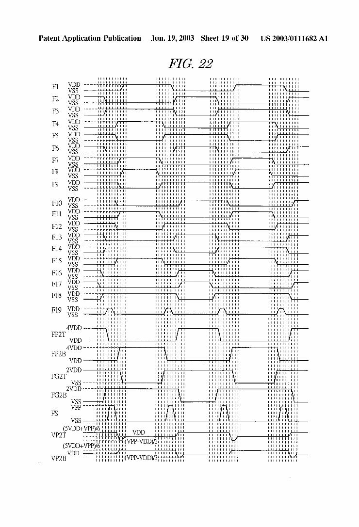
Patent Application Publication Jun. 19, 2003 Sheet 19 0f 30 US 2003/0111682 A1
vss VDD vss VDD vss
VDD vss
VDD vss VDD vss VDD vss VDD vss
VDD vss
VDD vss VDD vss VDD vss VDD vss VDD vss VDD vss
vnn vss VDD vss VDD vss
PS
VP2T
VPZB