EX1 - digsys.upc.esdigsys.upc.es/ed/CSD/terms/00_old/1112Q2/EX/EX_C/E… · Web viewMy signature...
20
EX1B: Designing standard combinational circuits DIGITAL CIRCUITS AND SYSTEMS EX1B: Designing standard combinational circuits 1.1 Cooperative group TEAM NUMBER: ___________ DUE DATE: ________________ 1 st review due date: ________________ STUDY TIME: Study time (in hours) Group work Classroom and laboratory sessions Out-of-class sessions Individu al Student 1 Student 2 Student 3 STATEMENT: My signature below indicates that I have (1) made an equitable contribution to EX1B as a member of the group, (2) read and fully agree with the contents (i.e., results, conclusions, analyses, simulations) of this document and (3) acknowledged by name anyone outside this group who assisted this learning team or any individual member in the completion of this document. Today’s date: __________________ Active members: Roles: (reporter, simulator, etc.) 1
Transcript of EX1 - digsys.upc.esdigsys.upc.es/ed/CSD/terms/00_old/1112Q2/EX/EX_C/E… · Web viewMy signature...

EX1B: Designing standard combinational circuits
DIGITAL CIRCUITS AND SYSTEMS
EX1B: Designing standard combinational circuits
1.1 Cooperative groupTEAM NUMBER: ___________
DUE DATE: ________________ 1st review due date: ________________
STUDY TIME:
Study time
(in hours)
Group work Classroom and laboratory sessions
Out-of-class sessions
Individual Student 1
Student 2
Student 3
STATEMENT:
My signature below indicates that I have (1) made an equitable contribution to EX1B as a member of the group, (2) read and fully agree with the contents (i.e., results, conclusions, analyses, simulations) of this document and (3) acknowledged by name anyone outside this group who assisted this learning team or any individual member in the completion of this document.
Today’s date: __________________
Active members: Roles: (reporter, simulator, etc.)
(1) ________________________________________ _______________
(2) _________________________________________ _______________
(3) _________________________________________ _______________
Acknowledgement of individual(s) who assisted this group in completing this document:
1

EETAC – Digital Circuits and Systems
(1) _______________________
(2) _______________________
1.2 Abstract Explain the most significant developments, results or conclusions about the exercise here. Use the remaining space on this sheet (200 words maximum).
(This section is mandatory. You must complete it in order to get a mark.)
2

EX1B: Designing standard combinational circuits
CONTENT
EX1B: Designing standard combinational circuits.....................................................................................1
1.1 Cooperative group.....................................................................................................................................1
1.2 Abstract.....................................................................................................................................................1
1.3 Description................................................................................................................................................3
1.4 Topics........................................................................................................................................................3
1.5 Part 1: Designing a small circuit...............................................................................................................5
1.5.1 Design options for a small circuit (flat design)................................................................................5
1.5.2 Synthesis into a CPLD or a FPGA....................................................................................................6
1.6 Part 2: Standard combinational blocks......................................................................................................6
1.6.1 Cascadable 1-bit comparator (COMP1)..........................................................................................6
1.6.2 4-channel multiplexer with enable input (MUX4)............................................................................7
1.6.3 2 to 4 decoder with enable input (DEC2:4)......................................................................................7
1.6.4 Hexadecimal to 7-segment display decoder......................................................................................7
1.6.5 1-bit binary adder (SUM1)................................................................................................................7
1.6.6 4-cahnnel demultiplexer with enable input (DEMUX4)...................................................................7
1.6.7 8 to 3 binary priority encoder with group select (GS) output (ENC8:3)..........................................7
1.6.8 9-bit even and odd parity generator..................................................................................................7
1.6.9 3-bit binary to Gray code converter..................................................................................................7
1.7 Part 3: Hierarchical design of complex combinational blocks..................................................................7
1.8 Problem solution (títol 2)..........................................................................................................................9
1.8.1 Part 1 (títol 3)....................................................................................................................................9
1.9 References.................................................................................................................................................9
1.10 Study plan to solve the exercise................................................................................................................9
1.11 Topics and activities checklist................................................................................................................10
1.12 Grading grid............................................................................................................................................11
1.13 Questions in solving EX1........................................................................................................................11
3

EETAC – Digital Circuits and Systems
1.3 DescriptionIn Section B of EX1, the basics of combinational circuits will be discussed. In Part 1, the process of implementing a small circuit into a PLD will be presented. The design will consist of a single VHDL file following a behavioural approach (truth table or algorithm) or a structural approach (logic circuit or equations). Part 2 will focus on the design of standard combinational components following the strategy of a flat design (a single VHDL file, as before). In Part 3, hierarchical design instantiating components will be used to generate a VHDL project consisting of multiple files. Thus, larger and more complex combinational circuits will be attained.
The problem also introduces the installation and use of the latest computer aided design (CAD) software to analyse, design and simulate combinational circuits and synthesise them into complex programmable logic devices (CPLD) or field-programmable gate arrays (FPGA):
- Minilog or Logic Friday (Espresso algorithm) to minimise logic equations.
- ISim embedded Xilinx simulator to run functional (behavioural) and gate-level (timing) simulations.
- Xilinx ISE and its integrated synthesis tool (XST) to implement logic circuits into PLD.
Finally, you will have the opportunity to use word processors, spell checkers, graphic tools and other auxiliary software to prepare documents that reflect the quality of your work.
Fig. 1 shows a summary of the most important concepts in this exercise.
Fig. 1 Flow chart to outline and clarify concepts studied in EX1B (Visio).
4

EX1B: Designing standard combinational circuits
1.4 Topics The following topics are listed based on the specific and cross-curricular learning objectives1 of the course: #1, #2, #3, #5, #6, #7. After studying Chapter 1 and successfully completing all the assignments in this task, you will be able to:
------------- Part 1: Your first VHDL project -------------
1. Explain the PLD design flow using Xilinx tools and training boards.
2. Search books and the Internet for information about the basics of VHDL language.
3. Explain the differences between the VHDL design styles (structural and behavioural).
4. Perform a functional (behavioural) simulation of a circuit in ISim using a VHDL test bench.
5. Perform a gate-level (timing) simulation of a logic circuit in ISim using a VHDL test bench.
6. Explain the concepts of flat design in a single VHDL file.
7. Explain and relate the following concepts for designing a logic circuit: truth table, Boolean algebra and logic functions, minimisation, SoP (sum of products) and PoS (product of sums), canonical algebraic equations, minterms and maxterms. Design concept map.
8. Simplify or minimize the logic function using software such as Minilog.exe.
------------- Part 2: Designing standard circuits -------------
9. Find the datasheets of the Small and Medium Scale of Integration (SSI and MSI) integrated circuits.
10. Design and use standard combinational circuit building blocks (at least one of them): multiplexers (or data selectors), demultiplexers (or data distributors), binary decoders and encoders, decoders for hexadecimal to seven-segment LED displays, code converters, adders, comparators, etc.
11. Use the HADES JAVA-based platform2 to visualise and analyse the operation of digital circuits.
12. Electrical characteristics of digital chips: voltages, power dissipation, propagation delays, etc.
13. Explain the basic technological details of a PLD and the main differences between a CPLD and FPGA.
-------------- Part 3: Hierarchical designs ------------
14. Produce a concept map (or a mind map) to explain a topic on the subject; for instance, to explain the advantages of using hardware description languages instead of electronic gate-level schematics.
15. Explain how to instantiate components in VHDL language. Hierarchical design: top-down design projects with more than one VHDL file.
1 http://digsys.upc.es/ed//CSD/units/CSD_Guia_docent_esborrany.doc
2 http://tams-www.informatik.uni-hamburg.de/applets/hades/webdemos/docs/tutorial.pdf
5

EETAC – Digital Circuits and Systems
-------------- Again… working effectively in groups ------------
16. Organise a plan to develop the exercise and to work efficiently in a team of two or three members using the proposed methodology.
17. Analyse individual and group study time.
18. Produce a high-quality written solution. For example, document your work using a predefined word processor template and utilities: spelling and grammar, chapter enumeration, page headers and footers, hyperlinks, cross-references, figure captions, text styles, etc., for a given exercise, control or any other assignment using the instructions given.
19. Assess individual and group learning progression and the quality of the deliverables.
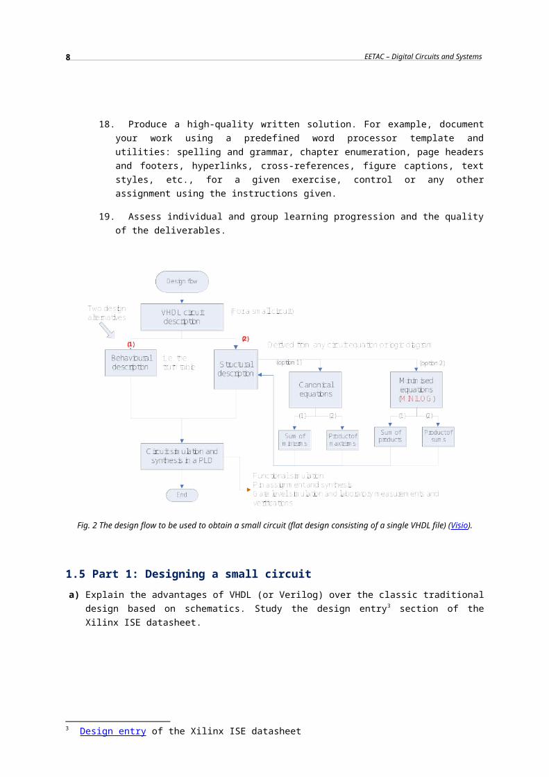
Fig. 2 The design flow to be used to obtain a small circuit (flat design consisting of a single VHDL file) (Visio).
1.5 Part 1: Designing a small circuit a) Explain the advantages of VHDL (or Verilog) over the classic traditional design based on schematics.
Study the design entry3 section of the Xilinx ISE datasheet.
3 Design entry of the Xilinx ISE datasheet
6
EX1B: Designing standard combinational circuits
a) b)
Fig. 3 Different formats to start a design in Xilinx ISE: a) using schematics (*.sch); b) using a HDL like VHDL (*.vhd)
1.5.1 Design options for a small circuit (flat design)
Design flow: (1) specifications (truth table, symbol, structural or behavioural approach); (2) functional simulation.
b) Design the example circuit from EX1A (Fig. 4) in several structural implementations and perform a functional simulation:
1. Canonical using minterms
2. Canonical using maxterms
3. Using Minilog, sum of products
4. Using Minilog, product of sums
5. Only NAND
6. Only NOR
c) Design the example circuit from EX1A in a behavioural implementation (directly stating the truth table, the circuit definition or its algorithm) and perform a functional simulation.
7
EETAC – Digital Circuits and Systems
Fig. 4 An example circuit to be redesigned.
NOTE: The assignment in Fig. 4 is only a sample of a simple combinational circuit. Your instructor may change it for a similar one. Your aim is to analyse the circuit proposed in class.
1.5.2 Synthesis into a CPLD or FPGA
Design flow: (3) pin assignment depending on the training board; (4) circuit synthesis; (5) gate-level simulation; (6) configuration file and CPLD/FPGA chip programming; (7) laboratory testing and measurements.
d) CPLD/FPGA pin assignment accordingly to any of the Digilent – Xilinx demonstration boards in use: NEXYS 2, Spartan-3AN Starter Kit, NI Digital Electronics FPGA Board, etc. Write down the main technology differences between CPLD and FPGA.
e) Gate-level simulation. Measure the maximum frequency of operation.
f) Laboratory measurements.
1.6 Part 2: Standard combinational blocks Every student in the cooperative group must be responsible for the design and testing of at least one combinational block. Study the small circuit design flow and the large circuit design flow in Unit 1.9 and Unit 1.10, respectively. As an example, see how a 1-bit comparator is designed.
1.6.1 Cascadable 1-bit comparator (COMP1)
1) Design step 1: Symbol, specifications and a similar commercial chip. The following information should be studied and analysed before you start designing a simple COMP1. The generic symbol of an n-bit cascadable comparator and its functionality can be seen in Fig. 5.
n(A<B)
(A=B)
E =
n
(A>B)
<
<
COMP
E
E=
nA
>
B
>
A B E< E= E> (A>B) (A=B) (A<B)
A>B X X X 1 0 0
A<B X X X 0 0 1
A=B 1 0 0 1 0 0
0 1 0 0 1 0
0 0 1 0 0 1
Fig. 5 Diagram of an n-bit cascadable comparator. Adapt the drawing to a COMP1 (1-bit comparator).
Find a similar commercial chip: Fig. 6 contains a representation of the commercial industry standard classic chip 74F85 (or 7485, 75S85, 74LS85, 74ALS85, etc.), which is a cascadable 4-bit binary comparator. Examine its datasheet and infer how it can be designed in VHDL as a COM1 using a circuit structure or a behavioural
8

EX1B: Designing standard combinational circuits
description. Read more information on comparators in Unit 1.11 of the old ED subject. Use the Java platform HADES from the University of Hamburg to learn how your circuit should work.
Fig. 6 Commercial 4-bit comparator 74F85 with “fast” TTL technology.
2) Design step 2: Write a proposal of the VHDL file depending on the internal structure or its behavioural description.
3) Design step 3: Propose a test bench and try to advance the ISim results on a sheet of paper.
4) Design step 4: Compile the ISE - ISim project and run a functional simulation to verify the previous hand-made timing diagram. Write comments on the waveforms to document your work.
At least in one of your projects:
5) Design step 5: Start the ISE project and run the Plan-Ahead application. Assign pins according to the training board that is going to be used.
6) Design step 6: Synthesise it using ISE XST (Xilinx Integrated Synthesis Tools) and check the RTL netlist drawing and the technology drawing.
7) Design step 7: Perform an ISim gate-level (timing) simulation with the corresponding propagation delay files to determine the maximum operation speed and to check the results with the ISE timing analyser tool.
8) Design step 8: Finish the COMP1 design flow in the laboratory and make measurements once the configuration file has been downloaded to the training board using Adept or iMPACT.
9

EETAC – Digital Circuits and Systems
1.6.2 4-channel multiplexer with enable input (MUX4)
1.6.3 2-to-4 decoder with enable input (DEC2:4)
1.6.4 Hexadecimal to 7-segment display decoder
1.6.5 1-bit binary adder (SUM1)
1.6.6 4-channel demultiplexer with enable input (DEMUX4)
1.6.7 8-to-3 binary priority encoder with group select (GS) output (ENC8:3)
1.6.8 9-bit even and odd parity generator
1.6.9 3-bit binary to Gray code converter
1.7 Part 3: Hierarchical design of complex combinational blocks Cooperative groups must choose a larger design that may be different and more complex than the ones chosen in Part 2. For instance, let us design the multiplexed display system for the four 7-segment LED digits installed in the NEXYS 2 board, as shown in Fig. 7.
Fig. 7 Connexion of the 7-segment digits to the Spartan 3E FPGA (source: NEXYS 2 datasheet).
This reference [3] and Fig. 8 give an idea of how to organise a hierarchical structure using smaller standard components. The counter will be introduced in EX2, so it has to be replaced here with a pair of switches.
10

EX1B: Designing standard combinational circuits
Fig. 8 Example block diagram for the 4-digit 7-segment display (source, Fig. 10.3).
g) Study the block diagram in Fig. 8 and redraw it using standard combinational components. Also draw the top entity named “display_driver”. Determine the number of VHDL files for this “display_driver_project”.
h) Invent or find every component on our web and test it using a functional simulation.
i) Apply the design flow in Unit 1.10, simulating the “display_driver” entity by means of a test bench. Test your design by downloading the synthesised circuit in the NEXYS 2 board.
Do not modify the text from page 3 to page 8
11

EETAC – Digital Circuits and Systems
1.8 Problem solution (títol 2)1.8.1 Part 1 (títol 3)
Part 1.1 (títol 4)
Start writing your solution here using the same template and conventions.
1.9 References Modify or add new references to this section. Follow the same format.
[1] http://digsys.upc.es . Comment: Course webpage that contains many resources, particularly materials from previous editions [retrieved October 2011].
[2] Brown, S., Vranesic, Z., “Fundamentals of digital logic with VHDL design”, McGraw-Hill, 2005. Comment: Figure 1.7 contains an example of a design flow for logic circuits and Figure 2.29 contains the structure of a typical CAD/EDA system.
[3] Haskell, R, E., Hanna, D. M., “Introduction to Digital Design using Digilent FPGA Boards", LBE Books, (http://www.lbebooks.com/booksandkits-HWDesignVHDL.htm#vhdlDigilentIntro )
[4] (add your own references here)
Remember that it is impossible to solve these exercises without consulting and studying books and technical materials. Thus, we expect you to write your references here.
1.10 Study plan to solve the exercise
12

EX1B: Designing standard combinational circuits
Check the documentation in our web [1] to look at ways to establish a study plan, a task distribution scheme and other requirements to succeed in producing a good solution when working cooperatively: flux diagrams, concept maps, schematics, tables, pictures, etc.
(This section is mandatory. It must be filled in to get a mark.)
13

EETAC – Digital Circuits and Systems
1.11 Topics and activities checklist
Topics Activities
Group member in
charge Comments
1 2 3
1. PLD design using Xilinx EDA tools and boards.
d)
2. Search books and the internet to learn about VHDL language. Advantages of VHDL over schematics.
b), Section 1.9
3. Structural and behavioural architectures b), c)
4. Functional simulation b), c)
5. Gate-level simulation e)
6. Flat design in a single VHDL file b), c)
7. Relate the following concepts for designing a logic circuit: truth table, Boolean algebra and logic functions, minimisation, SoP (sum of products) and PoS (product of sums), canonical algebraic equations, minterms and maxterms. Design concept map.
All the designs
8. Simplify or minimize logic function using software like Minilog.exe.
b), c) and other designs
9. Find the datasheets of SSI and MSI chips. Section 1.6
10. Standard combinational circuit building blocks (at least one of them): multiplexers, demultiplexers, decoders, encoders, code converters, adders, comparators, etc.
Section 1.6
11. Use the HADES JAVA-based platform to visualise and analyse the operation of digital circuits.
Section 1.6
12. Electrical characteristics of digital chips: voltages, power dissipation, propagation delays, etc.
e), f)
13. Technological differences between CPLD and FPGA.
d)
14. Produce a concept map (or mind map) to explain a topic on the subject.
Any
15. Hierarchical design instantiating components in VHDL language.
g), h), i)
14

EX1B: Designing standard combinational circuits
16. Organise a plan to work in a cooperative group for solving the exercises.
Sec. 1.10
17. Analyse your individual and group study time.
Sec. 1.10
18. Produce a quality written solution using this word processor template:
a. spelling and grammar
b. chapter enumeration
c. page headers and footers
d. hyperlinks
e. cross-references
f. figure captions
g. text styles for technical reports
(all of the document)
19. Assessing Secs. 1.11, 1.12 and
1.13
1.12 Grading grid
The exercise can be graded as follows.
Part 1: Design flow for a simple circuit
Part 2: Designing a small standard block
Part 3: A large and complex (hierarchical) combinational
circuit
Total
Scores 2p 4p 4p
Self-assessment
Instructor’s grades
1.13 Questions in solving EX1Reflect on the development of the exercise and how your cooperative group is coping with the task. Write your questions, comments, doubts, opinions, etc. here. Add more sheets if necessary to report on your progress or comments during the exercise. Hand in the exercise before the due date by uploading this “.docx” file to your e-Portfolio Google site.
15

EETAC – Digital Circuits and Systems
Aquests fulls de dubtes i d’explicació de com heu anat fent l’exercici són obligatoris. Si no és present, no es corregeix l’exercici i s’ha de tornar a lliurar. Abans de corregir i posar-vos qualificacions volem saber quin ha estat procés en què heu dissenyat els circuits i comparar-lo amb les nostres pròpies observacions de classe.
16