ENSC 495/851 Lab Electrical and Device …glennc/e495/e495la2n-testing.pdfFigure 12: NPN Bipolar, N...
8
ENSC 495/851 Lab Electrical and Device Measurements V1.0 Mar. 25 2015 Glenn Chapman Testing the devices is done after level 4 has been completed and wafers ENSC 495 students will do at least parts 1 to 5 on one chip. Graduates with a minor project the full set of tests on many positions. For the curve tracer use a digital camera to take the curve traces for the characteristics. Download the Tektronix 576 manuals to consult on using the curve tracer. Basic Chip Layout The ENSC 495/851 test chip layout (Figure 1) is a 5mm x 6mm (W x H). There will be more than 200 copies of this test chip on each wafer. The smallest feature size of these devices is 20 microns. Most lines are 40 microns wide. Figure 2 shows the labelled structures for the chip. Start with chips near the wafer centre. Figure 1: 5x6 mm ENSC 495/851 chip
Transcript of ENSC 495/851 Lab Electrical and Device …glennc/e495/e495la2n-testing.pdfFigure 12: NPN Bipolar, N...

ENSC 495/851 Lab Electrical and Device Measurements V1.0 Mar. 25 2015 Glenn Chapman
Testing the devices is done after level 4 has been completed and wafers ENSC 495 students will do at least parts 1 to 5 on one chip. Graduates with a minor project the full set of tests on many positions. For the curve tracer use a digital camera to take the curve traces for the characteristics. Download the Tektronix 576 manuals to consult on using the curve tracer. Basic Chip Layout The ENSC 495/851 test chip layout (Figure 1) is a 5mm x 6mm (W x H). There will be more than 200 copies of this test chip on each wafer. The smallest feature size of these devices is 20 microns. Most lines are 40 microns wide. Figure 2 shows the labelled structures for the chip. Start with chips near the wafer centre.
Figure 1: 5x6 mm ENSC 495/851 chip

Alig
P c
gnment
N resistan
ResoP
N
Con
comb
Metal resista
nce 4 pt.
olution targe
P resistance 4
Exposure L
Metal
P
ntact
30, 20 & 10
Fi
Metal com
nce 4 pt.
P tub
ets, layers 1, 2
4 pt. Contac
L’s
N
Contact
0μm
gure 2 ENSC
mb Metal
N comb
NP
2, 3
ct Diode
Layer #
495/851 test
step coverag
PN
Base
Em
Substrate contact
(collector)
t chip layout
ge
Solar Ce
N MOS
P MOS
mitter
ell
Repeat
SFacc
FU Thermal celerometer

Prober (Micromanipluators) The probes or micromanipulators (see Fig 2) consist of 3 axis controllers for X, Y and Z (up down) control (see Fig 2) at one end. Note the direction of motion is set by the arrows on the prober and may be different for different probes. The probe needle (Fig. 3) at the end is what makes contact and is roughly 5 um in size in this case. The probers can position within a micron if used right.
Figure 2: Micromanipulator probe
Figure 3: Probe needle in the prober

PBthsetr
(1Tseli
Probe TestinBefore startinhe contact paecond proberacer or ohm
1) SubstrateTest the Alumecond on thene in the IV
ng ng any measuad (has a C
e on the samm meter). Ch
e Contact minum is me bottom (Figploy. Meas
urements coabove it on
me contact paheck each pro
F
aking good g. 5). Use thsure the resis
Figure 5
onfirm the prthe chip) m
ad and makeobe this way
Figure 4: Con
contact to thhe curve tracstance by the
5: Ohmic co
robes are woaking good
e certain thay (this also g
ntact cuts and
he substratecer first to che slope and b
ntact compa
orking propecontact (ins
at you get a gets you used
diode pads
. Place oneheck for ohmby multimete
ared to non o
erly. To do ttructions in short betwee
d to putting t
e probe on tomic contact (er.
ohmic
this place onthe lab). Then them (usthe probes do
op contact p(see Fig 5), i
ne probe on hen place a e the curve own).
pad and the ie a straight

(2Um(acaproh
(3UcucuthfobrTretr
2) 4 Point ShUsing the 20measure sheeat top) are falculate the robe, Van dhmic contac
3) Large DioUsing the suburve tracer murve tracer shat there is orward and rreakdown vo
Then check feverse breakracer number
heet Resista0-micron Vaet resistance for the volta
sheet resistde Pauw, ancts with IV cu
Figure 6: V
ode bstrate contameasure the screen to recno leakage reverse voltaoltage (Fig. for reverse lkdown voltars and do no
ance an de Pauw
of the alumage, outer 2 tance for eand 4-Points turve
Van der Paw
act and the diode IV ch
cord the data(Fig 7). Fro
ages. Find t8). Note if
leakage (higge (good if
ot get a reflec
& 4-Point minum, boron
for the curach layer. Cotest structur
(2 on right)
diode (boroharacteristicsa. First takeom the photthe followingnot seeing a
gh curve trac> -5V, grea
ction of your
Kalvin resin diffusion arrent in the ompare the re) and com
and 4 point
on) contacts s. What is th
e a IV plot fotographs of g: forward rea diode curvecer amplificaat if > 20 Vrself in the p
stance test and phospho4 point multhree sets o
mment on the
t Kalvin (2 o
(see Figure he turn on v
for at a few vthe curve tresistance of e go try chipation) – at a
V). Be sure pictures.
structures shorus diffusioltimeter. Usof sheet resie difference
on left) test s
4) for the pvoltage? Takvolts to checracer take m
f the diode, rps at top, sidabout neg 0to take pho
hown in Figon layers. Inse dimensionistance valu
e observed.
tructures
probe contake a photogck for diodemeasurementreverse leakades or bottom.5 V. Final
otos showing
gure 4,6 to nner 2 pads ns given to
ues (4-point Check for
acts and the graph of the curve, and ts at a few age current, m of wafer. lly measure g the curve
F (4Uanvohoso
igure 7: IV d
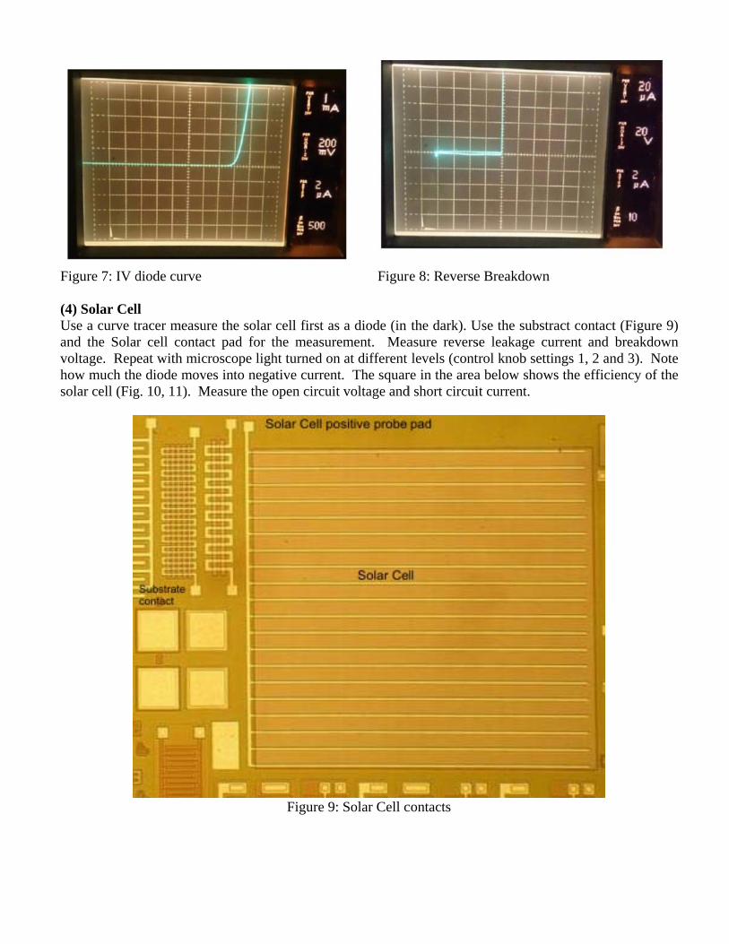
4) Solar CelUse a curve tnd the Solaoltage. Repow much theolar cell (Fig
diode curve
ll tracer measur cell contaeat with mice diode movg. 10, 11). M
ure the solar act pad for tcroscope lighves into negaMeasure the o
cell first as the measureht turned on ative currentopen circuit
Figure 9:
Figur
a diode (in ement. Mea
at different t. The squarvoltage and
Solar Cell c
e 8: Reverse
the dark). Uasure reverslevels (cont
re in the aread short circui
contacts
e Breakdown
Use the substse leakage ctrol knob seta below showit current.
n
tract contactcurrent and ttings 1, 2 anws the effici
t (Figure 9) breakdown
nd 3). Note iency of the

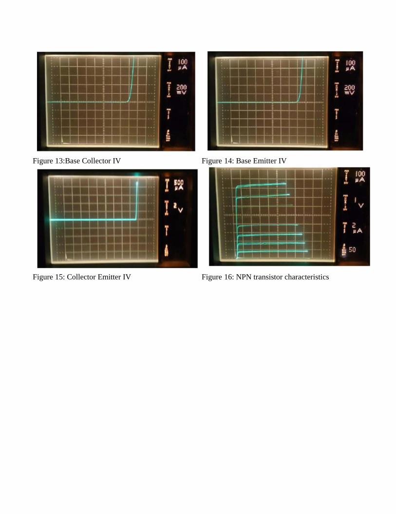
Figure 10: Solar cell diode Figure 11: Solar cell with light on. (5) NPN Transistor Test Test the dual-base-contact NPN transistor using the curve tracer. Use the substrate transistor contact as the collector (See Figure 12 for the Collector, Base and Emitter contacts). Measure the transistor characteristics (in the dark). Measure the Base Collector, Base Emitter and Collector Emitter IV characteristics (Fig 13-15). Watch for breakdown of CE curve (it may be bidirectional diode). The put curve tracer in NPN transistor mode and take full characteristics (Fig. 16) What do the transistor action characteristic curves look like (note the base current, collector current etc)? Calculate the transistor beta (current gain) at collector currents around 100µA and 3mA.
Figure 12: NPN Bipolar, N Mosfet and P Mosfet pads
F
F
igure 13:Bas
igure 15: Co
se Collector
ollector Emit
IV
tter IV
Figure
Figure
14: Base Em
16: NPN tra
mitter IV
ansistor charracteristics