Energia Fotovoltaica, MC Brito PV 20/10/1009 - ULisboasolar.fc.ul.pt/PV_course/PV classes -...
21
Energia Solar Fotovoltaica, MC Brito PV technologies 20/10/1009 Mestrado Integrado Engenharia da Energia e do Ambiente, Faculdade Ciências da Universidade de Lisboa, 1/22 PV TECHNOLOGIES PV TECHNOLOGIES Silicon Silicon solar solar cells cells Is there a c-Si technology? Feedstock Wafer Wafer Cells Module Other silicon concepts Materials availability PV TECHNOLOGIES PV TECHNOLOGIES Silicon Silicon solar solar cells cells Silicon purification Crystal growth Wafering Cell Siemens process Multicrystalline casting Wire saw Screenprint, BSF, SiN Semi-grade Si Union Carbide, FBR Multi Si Bridgeman, EM casting Solar-grade Si FBR (HSiCl3 ), UMGS VLD Mono Si CZ, 3-crystal Metallization Inkjet, PL, ti Selectivemitter, RTP, optical confinement... Silicon ribbons EFG, String Ribbon, RGS, DWeb, RST, SWeb, EZ, SDS, S’tile Crystalline silicon thin films Epitaxial growth or multicrystalline growth (annealing, metal induced, laser induced or zone melting recrystallization) UMGS, VLD CZ, 3 crystal Spherical Sliver evaporation Other concepts HIT, buried or point contact... Silicon nanoparticles (Innovalight)
Transcript of Energia Fotovoltaica, MC Brito PV 20/10/1009 - ULisboasolar.fc.ul.pt/PV_course/PV classes -...

Energia Solar Fotovoltaica, MC Brito PV technologies 20/10/1009
Mestrado Integrado Engenharia da Energia e do Ambiente, Faculdade Ciências da Universidade de Lisboa, 1/22
PV TECHNOLOGIESPV TECHNOLOGIESSiliconSilicon solar solar cellscells
Is there a c-Si technology? Feedstock Wafer Wafer Cells
Module Other silicon concepts Materials availability
PV TECHNOLOGIESPV TECHNOLOGIESSiliconSilicon solar solar cellscells
Siliconpurification
Crystal growth
Wafering Cell
Siemens process
Multicrystalline casting
Wire sawScreenprint,
BSF, SiN
Semi-grade Si Union
Carbide, FBR
Multi SiBridgeman, EM casting
Solar-grade SiFBR (HSiCl3 ),
UMGS VLD
Mono SiCZ, 3-crystal
Metallization Inkjet, PL,
ti
Selectivemitter,RTP, optical
confinement...
Silicon ribbonsEFG, String Ribbon, RGS,
DWeb, RST, SWeb, EZ, SDS, S’tile
Crystalline silicon thin filmsEpitaxial growth or multicrystalline growth (annealing,
metal induced, laser induced or zone melting recrystallization)
UMGS, VLDCZ, 3 crystal
Spherical
Sliver
evaporation
Other concepts HIT, buried or
point contact...
Silicon nanoparticles (Innovalight)

Energia Solar Fotovoltaica, MC Brito PV technologies 20/10/1009
Mestrado Integrado Engenharia da Energia e do Ambiente, Faculdade Ciências da Universidade de Lisboa, 2/22
PV TECHNOLOGIESPV TECHNOLOGIESSiliconSilicon solar solar cellscells
Silicon is the second most abundant element on Earth after oxygen (28% f th E th’(28% of the Earth’s crust). Its most familiar forms are sand and quartzite (the latter one is more pure).
PV TECHNOLOGIESPV TECHNOLOGIESSiliconSilicon solar solar cellscellsFeedstock: obtaining hyperpure silicon from
gas phase
Siemens process
Fluidizedbed reactor
PV TECHNOLOGIESPV TECHNOLOGIESSiliconSilicon solar solar cellscellsFeedstock: obtaining hyperpure silicon from
gas phase

Energia Solar Fotovoltaica, MC Brito PV technologies 20/10/1009
Mestrado Integrado Engenharia da Energia e do Ambiente, Faculdade Ciências da Universidade de Lisboa, 3/22
PV TECHNOLOGIESPV TECHNOLOGIESSiliconSilicon solar solar cellscells
Crystalline silicon may be used in PV in different forms:
Descriptor Symbol Grain SizeCommon Growth
TechniquesTechniques
Single crystal sc-Si >10cmCzochralski (CZ)
float zone (FZ)
Multicrystalline mc-Si 1mm-10cmCast, sheet,
ribbon
Polycrystalline pc-Si 1µm-1mmChemical-vapour
deposition
Microcrystalline µc-Si <1µm Plasma deposition
PV TECHNOLOGIESPV TECHNOLOGIESSiliconSilicon solar solar cellscells
Czochralski silicon is the standard for electronics industry. High quality (mono) with contamination with oxygen and carbon into th ltthe melt.
PV TECHNOLOGIESPV TECHNOLOGIESSiliconSilicon solar solar cellscells
Czochralski silicon Growth rate: 5cm/hour

Energia Solar Fotovoltaica, MC Brito PV technologies 20/10/1009
Mestrado Integrado Engenharia da Energia e do Ambiente, Faculdade Ciências da Universidade de Lisboa, 4/22
PV TECHNOLOGIESPV TECHNOLOGIESSiliconSilicon solar solar cellscells
Float zone silicon is the best quality silicon
No contamination but very expensive. Only for very demanding applications.
PV TECHNOLOGIESPV TECHNOLOGIESSiliconSilicon solar solar cellscells
Multicrystalline silicon offers acceptable quality but at lower cost
PV TECHNOLOGIESPV TECHNOLOGIESSiliconSilicon solar solar cellscells
Multicrystalline silicon offers acceptable quality but at lower cost.
Casting or direct solidification, requires careful thermal control Crucible usually made of quartzthermal control. Crucible usually made of quartz or graphite, often with Si3N4 coating.
Typical casting: 240kg/56 hours

Energia Solar Fotovoltaica, MC Brito PV technologies 20/10/1009
Mestrado Integrado Engenharia da Energia e do Ambiente, Faculdade Ciências da Universidade de Lisboa, 5/22
PV TECHNOLOGIESPV TECHNOLOGIESSiliconSilicon solar solar cellscells
Multicrystalline ingots require sawing.Kerf loss and saw damage removal is significant(and costly).
PV TECHNOLOGIESPV TECHNOLOGIESSiliconSilicon solar solar cellscells
Multicrystalline wafers may be grown directly in sheet or ribbon form.
Edge defined film fed growth (EFG)
String ribbon (SR)
Ribbon growth on substrate (RGS)
Dendritic web
Sheet silicon
…
PV TECHNOLOGIESPV TECHNOLOGIESSiliconSilicon solar solar cellscells
Multicrystalline wafers may be grown directly in sheet or ribbon form.
Edge defined film fed growth (EFG)

Energia Solar Fotovoltaica, MC Brito PV technologies 20/10/1009
Mestrado Integrado Engenharia da Energia e do Ambiente, Faculdade Ciências da Universidade de Lisboa, 6/22
PV TECHNOLOGIESPV TECHNOLOGIESSiliconSilicon solar solar cellscells
Multicrystalline wafers may be grown directly in sheet or ribbon form.
String ribbon (SR)
PV TECHNOLOGIESPV TECHNOLOGIESSiliconSilicon solar solar cellscells
Multicrystalline wafers may be grown directly in sheet or ribbon form.
Ribbon growth on substrate (RGS)
PV TECHNOLOGIESPV TECHNOLOGIESSiliconSilicon solar solar cellscells
Check:PVCDROMChapter 6

Energia Solar Fotovoltaica, MC Brito PV technologies 20/10/1009
Mestrado Integrado Engenharia da Energia e do Ambiente, Faculdade Ciências da Universidade de Lisboa, 7/22
PV TECHNOLOGIESPV TECHNOLOGIESSiliconSilicon solar solar cellscells
Typical screen printed silicon solar cell manufacturing process Saw damage etch Phosphorous diffusion Phosphorous diffusion Edge isolation Back contact print Firing Anti reflective coating Front contact print Firing Testing & sorting
PV TECHNOLOGIESPV TECHNOLOGIESSiliconSilicon solar solar cellscells
Phosphorous diffusion can be inline continuous or batch typeP source: POCl3P source: POCl3
PV TECHNOLOGIESPV TECHNOLOGIESSiliconSilicon solar solar cellscells
Screenprinting using silver paste is standard.Inkjet alternatives and/or th t i lother materials are
fashionable research topics.

Energia Solar Fotovoltaica, MC Brito PV technologies 20/10/1009
Mestrado Integrado Engenharia da Energia e do Ambiente, Faculdade Ciências da Universidade de Lisboa, 8/22
PV TECHNOLOGIESPV TECHNOLOGIESSiliconSilicon solar solar cellscells
Handling thin wafers and keeping high yields may be challenging
PV TECHNOLOGIESPV TECHNOLOGIESSiliconSilicon solar solar cellscells
PV silicon module
Packing density
Interconnection PV cells
Encapsulation
PV TECHNOLOGIESPV TECHNOLOGIESSiliconSilicon solar solar cellscells
PV silicon module
Packing density
Interconnection PV cells
Encapsulation

Energia Solar Fotovoltaica, MC Brito PV technologies 20/10/1009
Mestrado Integrado Engenharia da Energia e do Ambiente, Faculdade Ciências da Universidade de Lisboa, 9/22
PV TECHNOLOGIESPV TECHNOLOGIESSiliconSilicon solar solar cellscells
PV silicon module
Packing density
Interconnection PV cells
Encapsulation◦ Good transmittance but UV absorbance
◦ Rigidity to withstand mechanical loads
◦ Protection from weather agents and humidity
PV TECHNOLOGIESPV TECHNOLOGIESSiliconSilicon solar solar cellscells
Is there a c-Si technology?PERL solar cell
PV TECHNOLOGIESPV TECHNOLOGIESSiliconSilicon solar solar cellscells
Is there a c-Si technology?Buried contact solar cell

Energia Solar Fotovoltaica, MC Brito PV technologies 20/10/1009
Mestrado Integrado Engenharia da Energia e do Ambiente, Faculdade Ciências da Universidade de Lisboa,
10/22
PV TECHNOLOGIESPV TECHNOLOGIESSiliconSilicon solar solar cellscells
Is there a c-Si technology?Rear interdigitated (RISE) solar cell
PV TECHNOLOGIESPV TECHNOLOGIESSiliconSilicon solar solar cellscells
Is there a c-Si technology?Rear interdigitated (RISE) solar cell
PV TECHNOLOGIESPV TECHNOLOGIESSiliconSilicon solar solar cellscells
Is there a c-Si technology?Spheral solar cell

Energia Solar Fotovoltaica, MC Brito PV technologies 20/10/1009
Mestrado Integrado Engenharia da Energia e do Ambiente, Faculdade Ciências da Universidade de Lisboa,
11/22
PV TECHNOLOGIESPV TECHNOLOGIESSiliconSilicon solar solar cellscells
Is there a c-Si technology?Sliver solar cell
PV TECHNOLOGIESPV TECHNOLOGIESSiliconSilicon solar solar cellscellsMaterials availability Silicon is very abundant…
Silver paste for thecontacts will be a material bottleneck
Other (temporary) bottlenecks: ◦ Module glass
◦ Tedlar
◦ EVA
Andrea Feltrin, Alex Freundlich, Material considerations for terawatt level deployment of photovoltaics, Renewable Energy 33 (2008) 180–185
PV TECHNOLOGIESPV TECHNOLOGIESOtherOther technologiestechnologies
Other concepts, materials & technologies◦ a-Si
◦ CIGS◦ CIGS
◦ CdTe
It’s not only about efficiency (nor cost!)

Energia Solar Fotovoltaica, MC Brito PV technologies 20/10/1009
Mestrado Integrado Engenharia da Energia e do Ambiente, Faculdade Ciências da Universidade de Lisboa,
12/22
PV TECHNOLOGIESPV TECHNOLOGIESAmorphousAmorphous siliconsilicon solar solar cellscells Amorphous – commonly applied to
noncrystalline materials prepared by deposition from gases
First working a-Si based solar cell: Carlson D, Wronski C, Appl. Phys. Lett. 28, 671 (1976)
Cheaper deposition Hydrogenated amorphous silicon (a-
Si:H) has higher absorption coefficient than crystalline silicon – much thinner(<1m) solar cells are possible
PV TECHNOLOGIESPV TECHNOLOGIESAmorphousAmorphous siliconsilicon solar solar cellscells
p-i-n configuration Electron-hole pairs are generated in
the intrinsic ‘thick’ layer and
S t d b th b ilt l t i fi ld Separated by the built electric field
Because doped layers have very little diffusion length…

Energia Solar Fotovoltaica, MC Brito PV technologies 20/10/1009
Mestrado Integrado Engenharia da Energia e do Ambiente, Faculdade Ciências da Universidade de Lisboa,
13/22
PV TECHNOLOGIESPV TECHNOLOGIESAmorphousAmorphous siliconsilicon solar solar cellscells
Very thin active layer (<1m) thus: requires substrate
Substrate may be glass: useful for building integrated PV
Substrate may be glass: useful for flexible solar cells
PV TECHNOLOGIESPV TECHNOLOGIESAmorphousAmorphous siliconsilicon solar solar cellscells
To increase efficiency, more junctions(tandem configuration) may be added
A more modern & fashionable second layer: microcrystalline silicon layer
PV TECHNOLOGIESPV TECHNOLOGIESAmorphousAmorphous siliconsilicon solar solar cellscellsSignificant decline in their efficiency during their first few hundred hours of illumination: Staebler–Wronskieffect

Energia Solar Fotovoltaica, MC Brito PV technologies 20/10/1009
Mestrado Integrado Engenharia da Energia e do Ambiente, Faculdade Ciências da Universidade de Lisboa,
14/22
PV TECHNOLOGIESPV TECHNOLOGIESAmorphousAmorphous siliconsilicon solar solar cellscells
PECVD - Plasma enhanced chemical vapourdeposition (a.k.a. RF glow discharge deposition)
SiH4 + H2 into the chamber
RF is applied and generates plasma
plasma excites and decomposes the gas and generates radicals and ions
that will diffuse onto the
heated substrate
Typical growth speed: 1 angstrom/sec; Typical substrate temperature: 150-350ºC
PV TECHNOLOGIESPV TECHNOLOGIESAmorphousAmorphous siliconsilicon solar solar cellscells
PV TECHNOLOGIESPV TECHNOLOGIESAmorphousAmorphous siliconsilicon solar solar cellscellsIn summary: Low efficiency (for the same yield requires more area: module framing & encapsulation become relevant costs) Low cost (may be interesting if land availability is not an issue) Niche markets such as building integrated PV, consumer electronics (i.e. gadgets), flexible solar cells,…

Energia Solar Fotovoltaica, MC Brito PV technologies 20/10/1009
Mestrado Integrado Engenharia da Energia e do Ambiente, Faculdade Ciências da Universidade de Lisboa,
15/22
PV TECHNOLOGIESPV TECHNOLOGIESCadmium Telluride solar cellsCadmium Telluride solar cells
CdTe has a high absorption coefficient: thus very thin active layer Earliest paper on CdTe solar cell:
Loferski J, J. Appl. Phys. 27, 777–784 (1956)
Most ‘popular’ configuration: CdTe/CdS heterojunction (p-type CdTe and n-type CdS)
PV TECHNOLOGIESPV TECHNOLOGIESCadmium Telluride solar cellsCadmium Telluride solar cells
A. Morales-Acevedo, Thin film CdS/CdTe solar cells: Research perspectives, Solar Energy 80 (2006) 675–681

Energia Solar Fotovoltaica, MC Brito PV technologies 20/10/1009
Mestrado Integrado Engenharia da Energia e do Ambiente, Faculdade Ciências da Universidade de Lisboa,
16/22
PV TECHNOLOGIESPV TECHNOLOGIESCadmium Telluride solar cellsCadmium Telluride solar cells
PV TECHNOLOGIESPV TECHNOLOGIESCadmium Telluride solar cellsCadmium Telluride solar cells
PV TECHNOLOGIESPV TECHNOLOGIESCadmium Telluride solar cellsCadmium Telluride solar cells Top efficiencies: Cell 16.7% (NREL);
Module 10.9% (BP Solarex);
Best seller: First Solar
Main issues:
Cheapesttechnology in themarket (<1€/Wp)
‘Limited’ efficiency Limited efficiency
Reliability (lifetime)
Materials!! Toxic Cd
Rare Te
Window ofopportunity taken!
Energia Solar Fotovoltaica, MC Brito PV technologies 20/10/1009
Mestrado Integrado Engenharia da Energia e do Ambiente, Faculdade Ciências da Universidade de Lisboa,
17/22
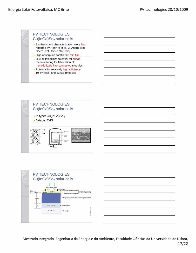
PV TECHNOLOGIESPV TECHNOLOGIESCu(Cu(InGaInGa)Se)Se22 solar cellssolar cells Synthesis and characterization were first
reported by Hahn H et al., Z. Anorg. Allg. Chem. 271, 153–170 (1953)
High absorption coefficient: thin filmg p
Like all thin films: potential for cheapmanufacturing for fabrication of monolithically interconnected modules
Potential for relatively high efficiency: 19.4% (cell) and 13.5% (module)
PV TECHNOLOGIESPV TECHNOLOGIESCu(Cu(InGaInGa)Se)Se22 solar cellssolar cells
P-type: Cu(InGa)Se2
N-type: CdS
PV TECHNOLOGIESPV TECHNOLOGIESCu(Cu(InGaInGa)Se)Se22 solar cellssolar cells

Energia Solar Fotovoltaica, MC Brito PV technologies 20/10/1009
Mestrado Integrado Engenharia da Energia e do Ambiente, Faculdade Ciências da Universidade de Lisboa,
18/22
PV TECHNOLOGIESPV TECHNOLOGIESCu(Cu(InGaInGa)Se)Se22 solar cellssolar cells Other different CIGS concepts…
PV TECHNOLOGIESPV TECHNOLOGIESOtherOther technologiestechnologies
CIGS nanoparticles Dye
Polymer solar cells
Many other different concepts…
Thin siliconfilm
Silicon nanoparticle
ink
DARPA (spectrum splitting)
Intermediate band cells
ysensitized solar cells
PV TECHNOLOGIESPV TECHNOLOGIESOtherOther technologiestechnologies

Energia Solar Fotovoltaica, MC Brito PV technologies 20/10/1009
Mestrado Integrado Engenharia da Energia e do Ambiente, Faculdade Ciências da Universidade de Lisboa,
19/22
PV TECHNOLOGIESPV TECHNOLOGIESComparingComparing differentdifferent technologiestechnologies
Cost
Performance/durability
Materials availability
Environmental issues
Maturity
Developers
Market penetration potential & others
PV TECHNOLOGIESPV TECHNOLOGIESEnergyEnergy paybackpayback timetime
V. Fthenakis, E. Alsema, Photovoltaics energy payback times, greenhouse gas emissions and external costs, Prog. Photovolt: Res. Appl. 2006; 14:275–280
PV TECHNOLOGIESPV TECHNOLOGIESEnergyEnergy paybackpayback timetime
l fl
timepaybackEnergyyieldEnergy
lifetimelOperationaygy

Energia Solar Fotovoltaica, MC Brito PV technologies 20/10/1009
Mestrado Integrado Engenharia da Energia e do Ambiente, Faculdade Ciências da Universidade de Lisboa,
20/22
PV TECHNOLOGIESPV TECHNOLOGIESMaterialsMaterials availabilityavailability
A.Feltrin, A.Freundlich, Material considerations for TW level deployment of PV, Renewable Energy 33 (2008) 180–185
Potential energy limits imposed by global silver (Ag) reserves for bulk-like silicon photovoltaic technologies. The orange shaded area represents limits reached using 50 mm-thick Ag ribbons. The green shaded area represents limits estimated using a 2 mm thick Ag electrodes and 5% grid shadowing.
PV TECHNOLOGIESPV TECHNOLOGIESMaterialsMaterials availabilityavailability
A.Feltrin, A.Freundlich, Material considerations for TW level deployment of PV, Renewable Energy 33 (2008) 180–185
PV TECHNOLOGIESPV TECHNOLOGIESMaterialsMaterials availabilityavailability
A.Feltrin, A.Freundlich, Material considerations for TW level deployment of PV, Renewable Energy 33 (2008) 180–185

Energia Solar Fotovoltaica, MC Brito PV technologies 20/10/1009
Mestrado Integrado Engenharia da Energia e do Ambiente, Faculdade Ciências da Universidade de Lisboa,
21/22
PV TECHNOLOGIESPV TECHNOLOGIESComparingComparing differentdifferent technologiestechnologiesConsidering all these factors… Silicon technologies are to dominate the market in the foreseeable future
Opportunities for other technologies with industrial l i i l CdT ( Fi S l )scale, in particular CdTe (e.g. First Solar)
Niche markets are breeding ground for other ‘new’ technologies (thin films in BIPV or flexible applications, concentration for large solar power plants, etc)
PV TECHNOLOGIESPV TECHNOLOGIESOtherOther technologiestechnologiesFurther reading Luque and Hegedus, Handbook of Photovoltaic Science and Engineering.
Edited by,John Wiley & Sons 2003 (Chp 6, 7, 12, 13, 14)
Goetzberger, Photovoltaic Solar Energy Conversion, Springer 2005 (Chp 3)
Sha et al, Thin-film silicon solar cell technology, Prog. Photovolt: Res. Appl. 2004; 12:113 142 (DOI: 10 1002/pip 533)2004; 12:113–142 (DOI: 10.1002/pip.533)
Bosio et al, Polycrystalline CdTe thin films for photovoltaic applications, Progress in Crystal Growth and Characterization of Materials, 52 (2006) 247-279
Morales-Acevedo, Thin film CdS/CdTe solar cells: Research perspectives, Solar Energy 80 (2006) 675–681
Fthenakis, E. Alsema, Photovoltaics energy payback times, greenhouse gas emissions and external costs, Prog. Photovolt: Res. Appl. 2006; 14:275–280[Check Fthenakis’s page: www.bnl.gov/pv
Feltrin, Freundlich, Material considerations for TW level deployment of PV, Renewable Energy 33 (2008) 180–185
Some Some ideasideas to explore to explore ininADVANCED TOPICSADVANCED TOPICS Processes & Concepts
Upgraded metalurgic silicon, silicon thin films, advanced silicon solar cell concepts, nano solar cells, very high efficiency solar cells, third generation concepts, etc
Environamental issuesPayback times, GHG emissions, pollution, recycling, etc
Material issuesAvailability, toxicity, graphene, etc
NREAP – Action plan for 2020 VLS-PV in the deset