Enabling large-scale deployment of photonics through cost ... · August, 2015 © 2015 IBM...
26
© 2015 IBM Corporation August, 2015 Enabling large-scale deployment of photonics through cost-efficient and scalable packaging T. Barwicz , Y. Taira, T. W. Lichoulas, N. Boyer, H. Numata, Y. Martin, J.-W. Nah, S. Takenobu, A. Janta-Polczynski, E. L. Kimbrell, R. Leidy, M. Khater, S. Kamlapurkar, S. Engelmann, Y. A. Vlasov, P. Fortier Silicon Nanophotonic Packaging
Transcript of Enabling large-scale deployment of photonics through cost ... · August, 2015 © 2015 IBM...
© 2015 IBM CorporationAugust, 2015
Enabling large-scale deployment of photonics through cost-efficient and scalable packaging
T. Barwicz, Y. Taira, T. W. Lichoulas, N. Boyer, H. Numata, Y. Martin, J.-W. Nah, S. Takenobu, A. Janta-Polczynski, E. L. Kimbrell, R. Leidy, M. Khater, S. Kamlapurkar, S. Engelmann, Y. A. Vlasov, P. Fortier
Silicon Nanophotonic Packaging
© 2015 IBM CorporationTymon Barwicz et al.,
Cost-Efficient Photonic Packaging August, 2015
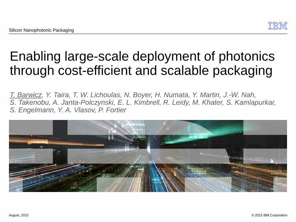
Cost can hinder the societal impact of a technology
2
Cost is not just a commercial concern. It defines the accessibility of a technology.Today’s challenge in optics: accessibility reduce cost by 10-100X major impact
Tesla Motors, Tesla Roadster 2.5Adapted from Winzer, OPN 2015
1986 1994 2002 2010 20181
10
100
1
10
100
Tb/s
Gb/
s
Telecom fiber capacityCost can define impact
First highway-capable electric vehicle• $109k+ ~2400 sold (2008-2012)• critical debut limited Earth impact
• massive bandwidth • cost prevents widespread applications
© 2015 IBM CorporationTymon Barwicz et al.,
Cost-Efficient Photonic Packaging August, 2015
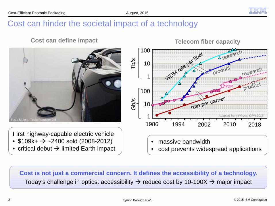
Integration is changing the cost structure of optical devices
3
Cost structure of legacy devices from discreet components
Impact of photonic integration less components, assembly, testing
Impact of silicon photonicCMOS made Si fabrication reliable and cheap large scale integration tiny cost
• Major cost reduction across the board with Si photonics.• Some cost elements remain unchanged limiting factor.
Cos
t
100G legacy
100G-LR4
Si Phot. 100G
Discreet components
Assembly
Testing
10G SONET transponderlightwavestore.com
© 2015 IBM CorporationTymon Barwicz et al.,
Cost-Efficient Photonic Packaging August, 2015
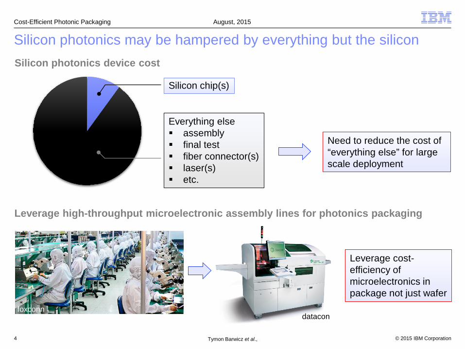
Silicon photonics may be hampered by everything but the silicon
4
Silicon photonics device cost
Silicon chip(s)
Everything else assembly final test fiber connector(s) laser(s) etc.
Need to reduce the cost of “everything else” for large scale deployment
Leverage high-throughput microelectronic assembly lines for photonics packaging
foxconndatacon
Leverage cost-efficiency of microelectronics in package not just wafer
© 2015 IBM CorporationTymon Barwicz et al.,
Cost-Efficient Photonic Packaging August, 2015
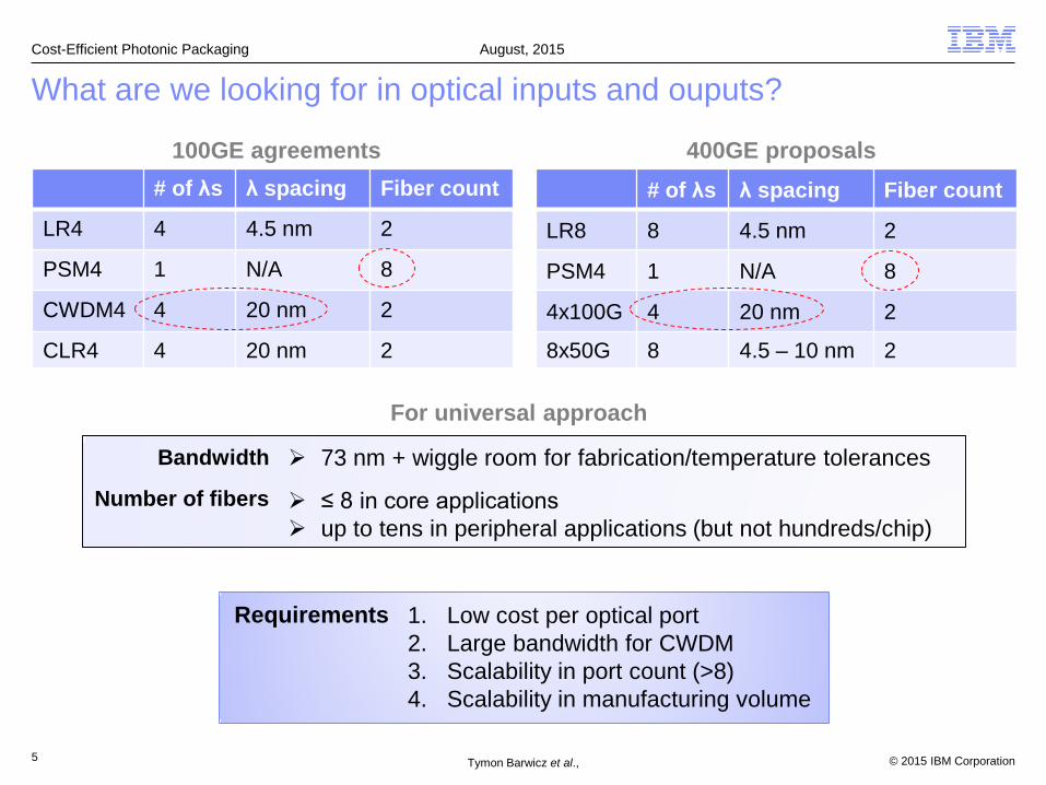
What are we looking for in optical inputs and ouputs?
5
# of λs λ spacing Fiber count
LR4 4 4.5 nm 2
PSM4 1 N/A 8
CWDM4 4 20 nm 2
CLR4 4 20 nm 2
# of λs λ spacing Fiber count
LR8 8 4.5 nm 2
PSM4 1 N/A 8
4x100G 4 20 nm 2
8x50G 8 4.5 – 10 nm 2
100GE agreements 400GE proposals
1. Low cost per optical port2. Large bandwidth for CWDM 3. Scalability in port count (>8)4. Scalability in manufacturing volume
Requirements
73 nm + wiggle room for fabrication/temperature tolerancesBandwidth
Number of fibers ≤ 8 in core applications up to tens in peripheral applications (but not hundreds/chip)
For universal approach
© 2015 IBM CorporationTymon Barwicz et al.,
Cost-Efficient Photonic Packaging August, 2015
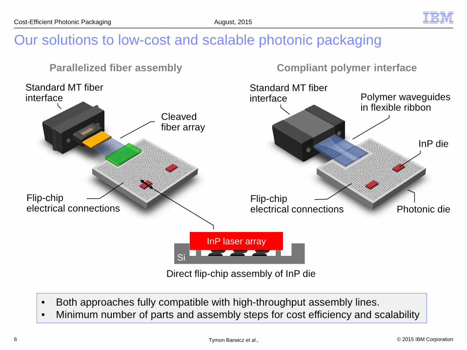
Our solutions to low-cost and scalable photonic packaging
6
• Both approaches fully compatible with high-throughput assembly lines.• Minimum number of parts and assembly steps for cost efficiency and scalability
Flip-chipelectrical connections
Standard MT fiber interface
Flip-chipelectrical connections
Standard MT fiber interface
Cleaved fiber array
Direct flip-chip assembly of InP die
Polymer waveguides in flexible ribbon
Photonic die
InP laser array
Si
Parallelized fiber assembly Compliant polymer interface
InP die
© 2015 IBM CorporationTymon Barwicz et al.,
Cost-Efficient Photonic Packaging August, 2015
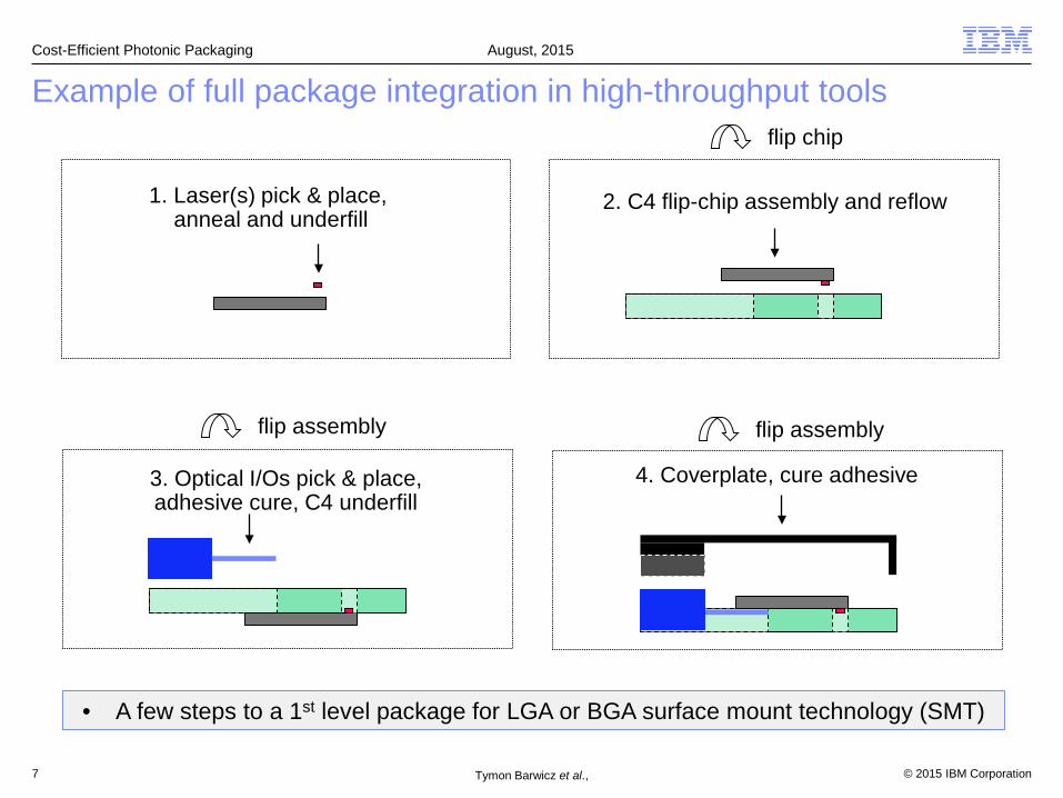
Example of full package integration in high-throughput tools
7
1. Laser(s) pick & place, anneal and underfill
flip chip
2. C4 flip-chip assembly and reflow
3. Optical I/Os pick & place,adhesive cure, C4 underfill
flip assembly
4. Coverplate, cure adhesive
flip assembly
• A few steps to a 1st level package for LGA or BGA surface mount technology (SMT)

© 2015 IBM CorporationTymon Barwicz et al.,
Cost-Efficient Photonic Packaging August, 2015
Main challenges to leveraging high-throughput tools for photonics
8
1. Limited placement accuracy of ± 10 um
Photonic chip
Polymer ribbon
10 um fiber mode
Mode expansionon wafer
Connect at largest mode for tolerances
2. Inflexible pick-and-place handling
Avoid small-mode fibers for cost and tolerances
Vacuum pick-tip handling Pressure-sensing movement only vertical
Integrate polymer lid for fiber handling
Vacuumpicktip
Chip assembly
Self-alignment for 1-2 um accuracy Mode engineering for max tolerances

© 2015 IBM CorporationTymon Barwicz et al.,
Cost-Efficient Photonic Packaging August, 2015
9
Parallelized fiber assembly: details
• Low cost pick-and-place assembly in high-throughput tools (T.Barwicz et al. ECTC 2015)• Arbitrary number of fibers in 1D array, in-plane coupling for CWDM bandwidth.
Polymer lid
Fiber ribbon
Cleaved ends InP attach region
V-groove array
Flip-chip electrical interface
Standard MT fiber interface
Photonic die
1 2
3
InP die
InP die
© 2015 IBM CorporationTymon Barwicz et al.,
Cost-Efficient Photonic Packaging August, 2015
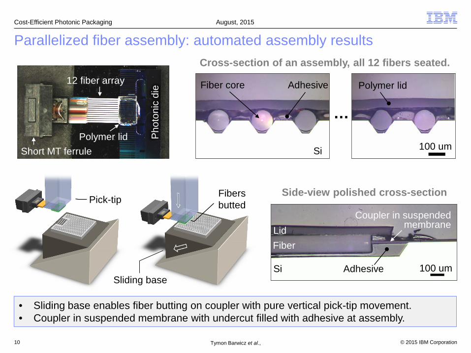
Fibersbutted
10
Parallelized fiber assembly: automated assembly results
• Sliding base enables fiber butting on coupler with pure vertical pick-tip movement.• Coupler in suspended membrane with undercut filled with adhesive at assembly.
Phot
onic
die
12 fiber array
Polymer lidShort MT ferrule
Side-view polished cross-section
FiberLid
Si Adhesive
Coupler in suspendedmembrane
100 um
Pick-tip
Sliding base
…
Fiber core
Si
Adhesive
100 um
Polymer lid
Cross-section of an assembly, all 12 fibers seated.

© 2015 IBM CorporationTymon Barwicz et al.,
Cost-Efficient Photonic Packaging August, 2015
Parallelized fiber assembly: fiber self-alignment in action
11
• Can re-align fiber offsets of up to ~40 um.• Concept implemented in a common R&D flip-chip bonder
Pick tip
Polymer lid
Fiber
V-groove
Si photonicchip
Pick tip reflection
© 2015 IBM CorporationTymon Barwicz et al.,
Cost-Efficient Photonic Packaging August, 2015
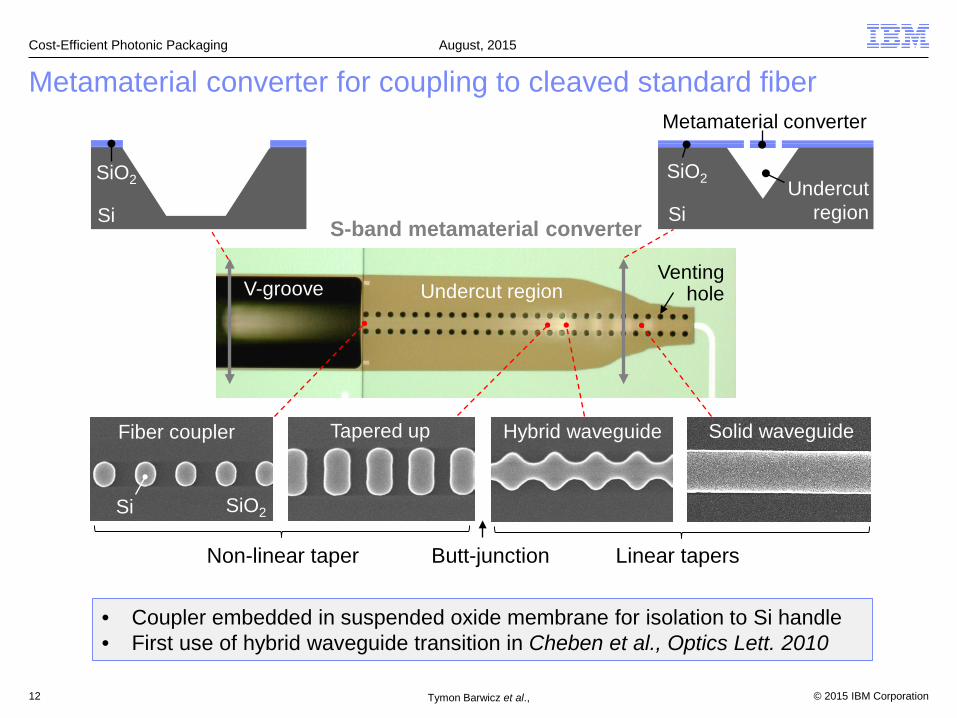
V-groove Undercut regionVenting
hole
Metamaterial converter for coupling to cleaved standard fiber
• Coupler embedded in suspended oxide membrane for isolation to Si handle• First use of hybrid waveguide transition in Cheben et al., Optics Lett. 2010
Fiber coupler Hybrid waveguide Solid waveguide
Metamaterial converter
UndercutregionSiSi
SiO2SiO2
Tapered up
12
Si SiO2
Non-linear taper Linear tapersButt-junction
S-band metamaterial converter

© 2015 IBM CorporationTymon Barwicz et al.,
Cost-Efficient Photonic Packaging August, 2015
Optical measurements of metamaterial converter performance
13
Wavelength (um)
Loss
to fi
ber (
dB)
1.26 1.28 1.3 1.32 1.34 1.36
-3
-2
-1
TETM
0.8 dB
-1.3 dB
O-band converter response
Measurement setup
Jig for pressing fibers into grooves
• Manual assembly to V-grooves, no active alignment (OFC’15, Th3F.3).
• Spread on single wafer: -1.1 dB to -2.6 dB• V-groove variability expected to dominate spread
in this early production tools implementation
Chip ID 1 2 3 4 5
Max in polarization -1.1 dB -1.2 dB -1.1 dB -2.4 dB -1.9 dB
Min in polarization -1.4 dB -1.5 dB -1.4 dB -2.6 dB -2.1 dB
Position on wafer random random random edge edge
1.31 um measurement with water immersion (n~1.31)
© 2015 IBM CorporationTymon Barwicz et al.,
Cost-Efficient Photonic Packaging August, 2015
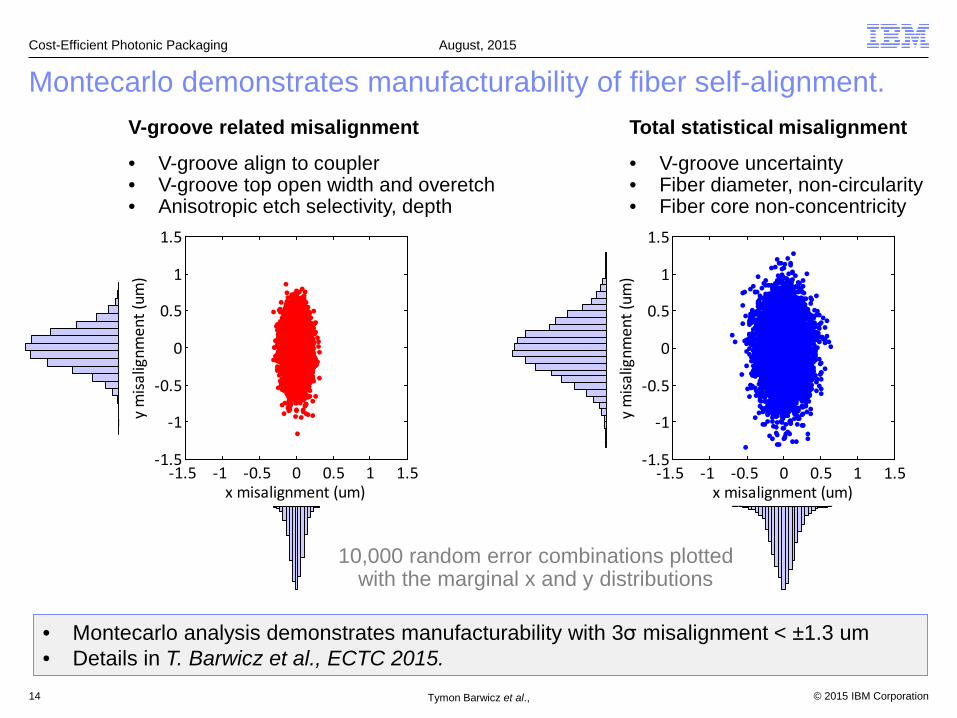
Montecarlo demonstrates manufacturability of fiber self-alignment.
14
-1.5 -1 -0.5 0 0.5 1 1.5-1.5
-1
-0.5
0
0.5
1
1.5
x misalignment (um)
y m
isalig
nmen
t (um
)
V-groove related misalignment (Montecarlo)
-1.5 -1 -0.5 0 0.5 1 1.5-1.5
-1
-0.5
0
0.5
1
1.5
x misalignment (um)
y m
isalig
nmen
t (um
)
Total fiber core to waveguide misalignment
-V-groove related misalignment
• V-groove align to coupler• V-groove top open width and overetch• Anisotropic etch selectivity, depth
Total statistical misalignment
• V-groove uncertainty• Fiber diameter, non-circularity• Fiber core non-concentricity
10,000 random error combinations plotted with the marginal x and y distributions
• Montecarlo analysis demonstrates manufacturability with 3σ misalignment < ±1.3 um• Details in T. Barwicz et al., ECTC 2015.
© 2015 IBM CorporationTymon Barwicz et al.,
Cost-Efficient Photonic Packaging August, 2015
15
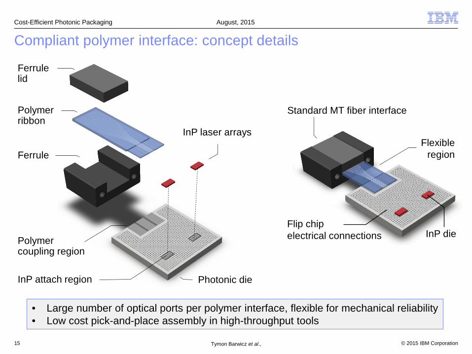
Compliant polymer interface: concept details
Flexibleregion
Standard MT fiber interface
Flip chipelectrical connections
• Large number of optical ports per polymer interface, flexible for mechanical reliability• Low cost pick-and-place assembly in high-throughput tools
Polymer ribbon
Ferrule
Polymer coupling region
InP laser arrays
InP attach region Photonic die
Ferrule lid
InP die
© 2015 IBM CorporationTymon Barwicz et al.,
Cost-Efficient Photonic Packaging August, 2015
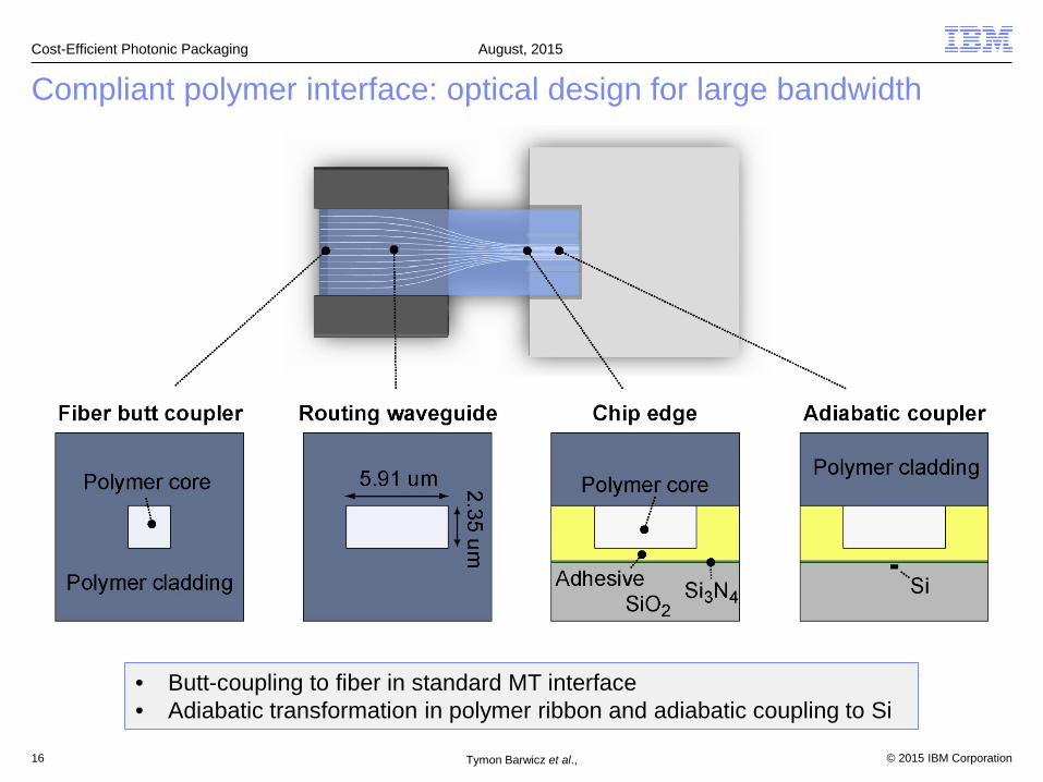
16
Compliant polymer interface: optical design for large bandwidth
• Butt-coupling to fiber in standard MT interface• Adiabatic transformation in polymer ribbon and adiabatic coupling to Si
© 2015 IBM CorporationTymon Barwicz et al.,
Cost-Efficient Photonic Packaging August, 2015
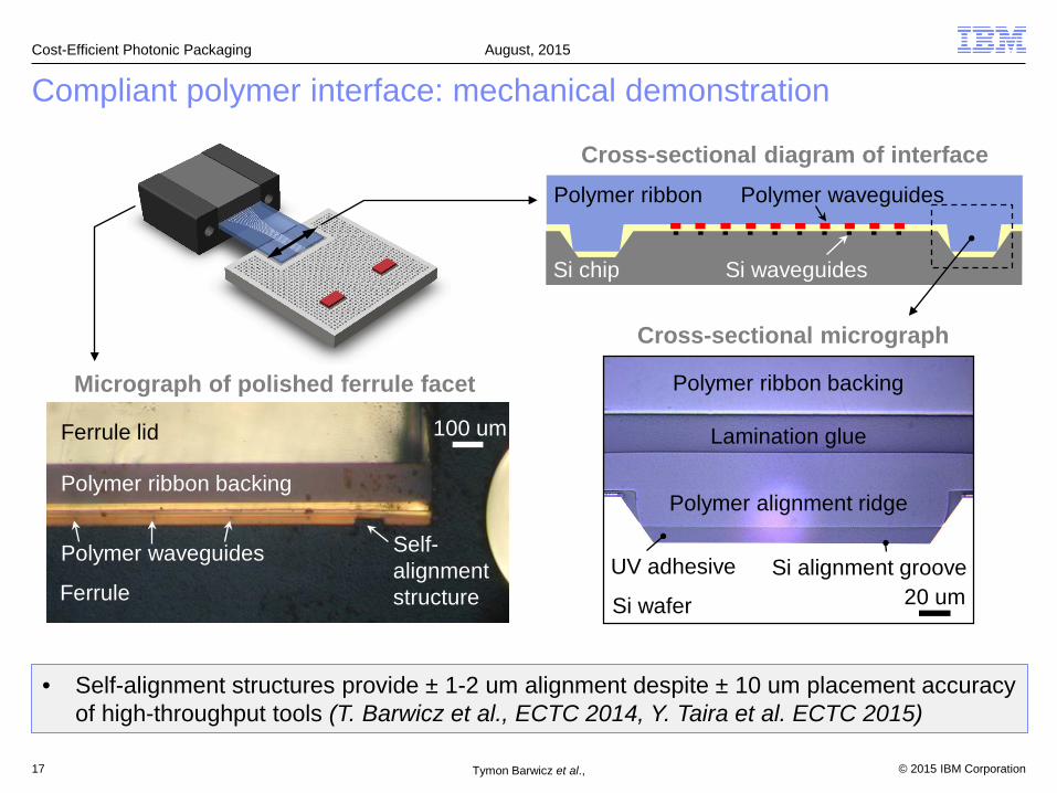
17
Compliant polymer interface: mechanical demonstration
• Self-alignment structures provide ± 1-2 um alignment despite ± 10 um placement accuracy of high-throughput tools (T. Barwicz et al., ECTC 2014, Y. Taira et al. ECTC 2015)
Self-alignment structureFerrule
Ferrule lid
Polymer ribbon backing
Polymer waveguides Self-alignment structure
Si alignment groove
Polymer alignment ridge
Polymer ribbon backing
Lamination glue
Si wafer 20 umUV adhesive
Si chip
Polymer ribbon
Si waveguides
Polymer waveguides
100 um
Cross-sectional diagram of interface
Micrograph of polished ferrule facet
Cross-sectional micrograph
© 2015 IBM CorporationTymon Barwicz et al.,
Cost-Efficient Photonic Packaging August, 2015
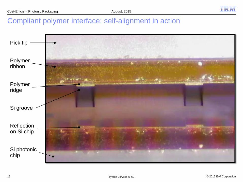
Compliant polymer interface: self-alignment in action
18
Pick tip
Polymerribbon
Si photonicchip
Polymerridge
Si groove
Reflectionon Si chip

© 2015 IBM CorporationTymon Barwicz et al.,
Cost-Efficient Photonic Packaging August, 2015
Compliant polymer interface: optical demonstration
19
Polymer ribbon
Automated assembly
Active alignment
1
2
Standard MTP connector
• Large bandwidth compatible with CWDM• Unexpected polarization dependence at
long wavelengths• Need design and assembly tweaks
Wavelength (um)Lo
ss fr
om fi
ber t
o si
licon
(dB)1.47 1.49 1.51 1.53 1.55 1.57
-4.5
-4
-3.5
-3
-2.5
-2
TETM
Scattering at abrupt chip-edge transition
Typical spectral response
Polymertransparency
OFC’15, Th3F.5
© 2015 IBM CorporationTymon Barwicz et al.,
Cost-Efficient Photonic Packaging August, 2015
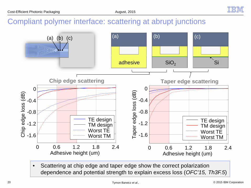
Compliant polymer interface: scattering at abrupt junctions
20
• Scattering at chip edge and taper edge show the correct polarization dependence and potential strength to explain excess loss (OFC’15, Th3F.5)
Adhesive height (um)
Chi
p ed
ge lo
ss (d
B)
0 0.6 1.2 1.8 2.4
-1.6
-1.2
-0.8
-0.4
0
TE designTM designWorst TEWorst TM
Adhesive height (um)
Tape
r edg
e lo
ss (d
B)
0 0.6 1.2 1.8 2.4
-1.6
-1.2
-0.8
-0.4
0
TE designTM designWorst TEWorst TM
adhesive SiO2 Si
(a) (b) (c) (a) (b) (c)
Chip edge scattering Taper edge scattering
© 2015 IBM CorporationTymon Barwicz et al.,
Cost-Efficient Photonic Packaging August, 2015
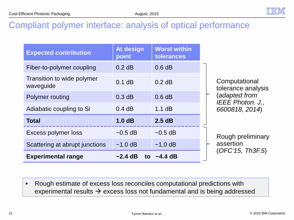
Compliant polymer interface: analysis of optical performance
21
Expected contribution At design point
Worst within tolerances
Fiber-to-polymer coupling 0.2 dB 0.6 dB
Transition to wide polymer waveguide 0.1 dB 0.2 dB
Polymer routing 0.3 dB 0.6 dB
Adiabatic coupling to Si 0.4 dB 1.1 dB
Total 1.0 dB 2.5 dB
Excess polymer loss ~0.5 dB ~0.5 dB
Scattering at abrupt junctions ~1.0 dB ~1.0 dB
Experimental range ~2.4 dB to ~4.4 dB
Rough preliminary assertion(OFC’15, Th3F.5)
Computational tolerance analysis(adapted fromIEEE Photon. J., 6600818, 2014)
• Rough estimate of excess loss reconciles computational predictions with experimental results excess loss not fundamental and is being addressed
© 2015 IBM CorporationTymon Barwicz et al.,
Cost-Efficient Photonic Packaging August, 2015
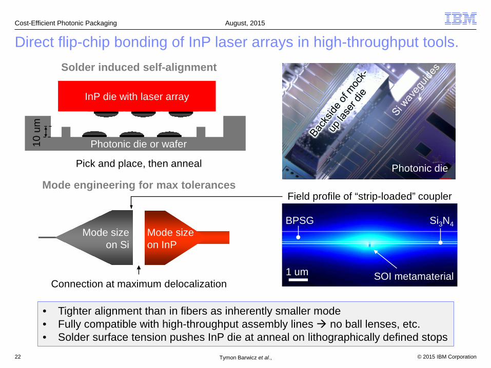
Direct flip-chip bonding of InP laser arrays in high-throughput tools.
22
Pick and place, then anneal
InP die with laser array
Photonic die or wafer10 u
m
Mode sizeon Si
Mode size on InP
Connection at maximum delocalization
Solder induced self-alignment
• Tighter alignment than in fibers as inherently smaller mode• Fully compatible with high-throughput assembly lines no ball lenses, etc.• Solder surface tension pushes InP die at anneal on lithographically defined stops
Mode engineering for max tolerancesPhotonic die
1 um
Field profile of “strip-loaded” coupler
SOI metamaterial
BPSG Si3N4
© 2015 IBM CorporationTymon Barwicz et al.,
Cost-Efficient Photonic Packaging August, 2015
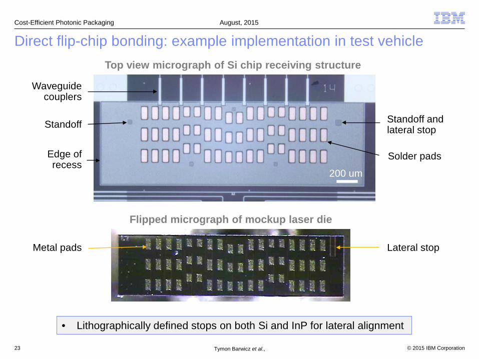
Direct flip-chip bonding: example implementation in test vehicle
23
• Lithographically defined stops on both Si and InP for lateral alignment
Top view micrograph of Si chip receiving structure
Flipped micrograph of mockup laser die
Standoff and lateral stop
Lateral stop
Solder pads
Standoff
Waveguide couplers
Edge of recess
Metal pads
200 um
© 2015 IBM CorporationTymon Barwicz et al.,
Cost-Efficient Photonic Packaging August, 2015
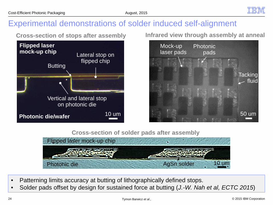
Experimental demonstrations of solder induced self-alignment
24
• Patterning limits accuracy at butting of lithographically defined stops.• Solder pads offset by design for sustained force at butting (J.-W. Nah et al, ECTC 2015)
10 um
Vertical and lateral stop on photonic die
Lateral stop on flipped chip
Photonic die/wafer
Flipped laser mock-up chip
Butting
Cross-section of stops after assembly Infrared view through assembly at anneal
Cross-section of solder pads after assembly
10 um
Photonic pads
Mock-up laser pads
Tacking fluid
50 um
AgSn solderPhotonic die
Flipped laser mock-up chip
© 2015 IBM CorporationTymon Barwicz et al.,
Cost-Efficient Photonic Packaging August, 2015
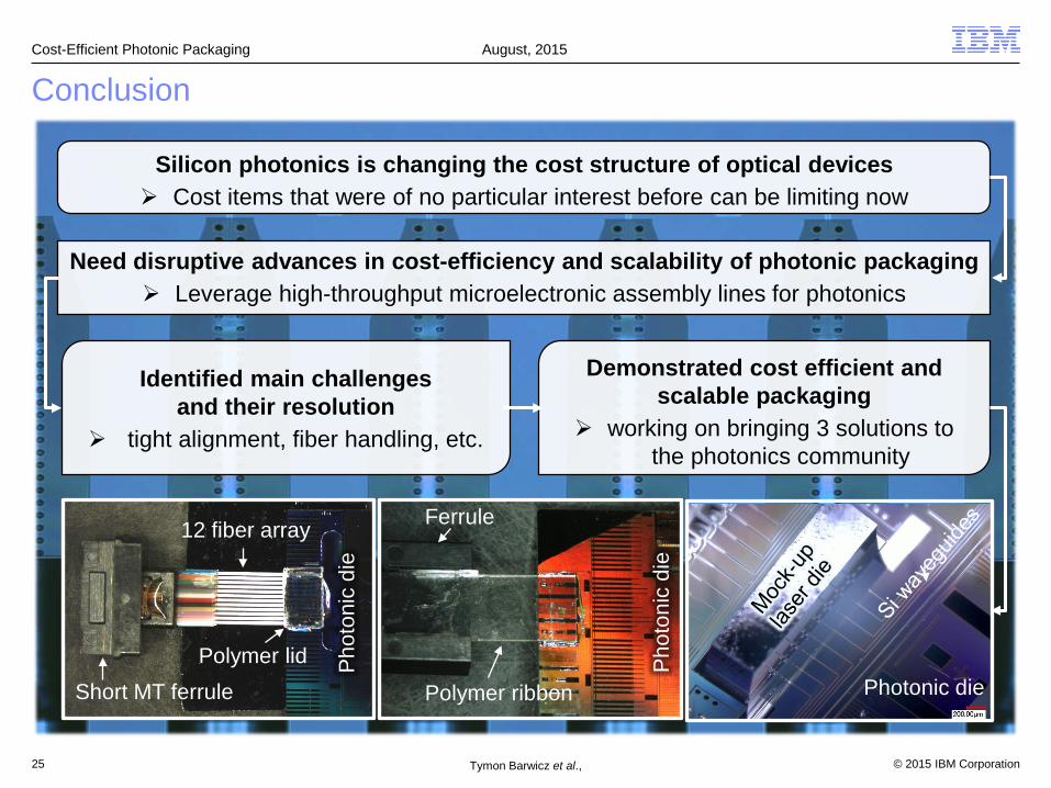
Conclusion
25
Phot
onic
die
12 fiber array
Polymer lidShort MT ferrule Photonic die
Phot
onic
die
Polymer ribbon
Ferrule
Identified main challenges and their resolution
tight alignment, fiber handling, etc.
Need disruptive advances in cost-efficiency and scalability of photonic packaging Leverage high-throughput microelectronic assembly lines for photonics
Silicon photonics is changing the cost structure of optical devices Cost items that were of no particular interest before can be limiting now
Demonstrated cost efficient and scalable packaging
working on bringing 3 solutions to the photonics community
© 2015 IBM CorporationTymon Barwicz et al.,
Cost-Efficient Photonic Packaging August, 2015
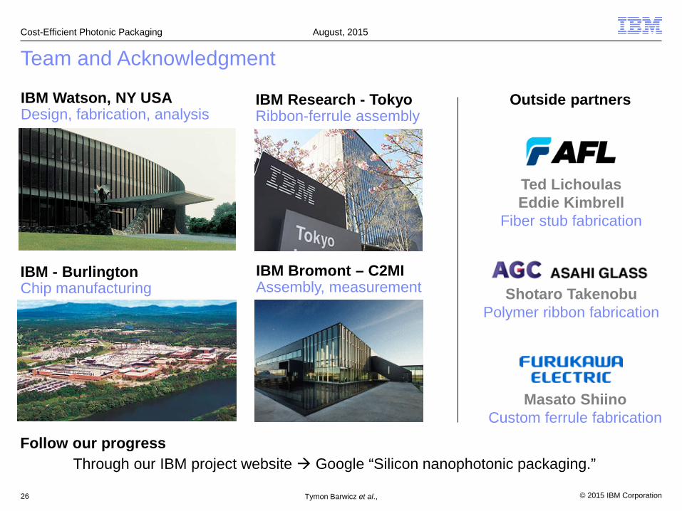
Team and Acknowledgment
26
IBM Watson, NY USADesign, fabrication, analysis
IBM - BurlingtonChip manufacturing
IBM Bromont – C2MIAssembly, measurement
Follow our progressThrough our IBM project website Google “Silicon nanophotonic packaging.”
IBM Research - TokyoRibbon-ferrule assembly
Outside partners
Shotaro TakenobuPolymer ribbon fabrication
Masato ShiinoCustom ferrule fabrication
Ted LichoulasEddie Kimbrell
Fiber stub fabrication