EN / PVS800 central inverters firmware manual...10 Introduction to the manual Target audience This...
208
ABB solar inverters Firmware manual PVS800 central inverters
Transcript of EN / PVS800 central inverters firmware manual...10 Introduction to the manual Target audience This...

ABB solar inverters
Firmware manualPVS800 central inverters

List of related manuals
Hardware manuals and guides Code (English)
PVS800-57 hardware manual 3AUA0000053689
Firmware manuals and guides
PVS800 firmware manual 3AUA0000058422
Application guide: Adaptive program for PVS800 3AUA0000091276
Option manuals and guides
RETA-01 Ethernet Adapter Module User's Manual 3AFE64539736
RMBA-01 Modbus Adapter Module User's Manual 3AFE64498851
NETA-21 Remote Monitoring Tool User’s manual 3AUA0000096939
Manuals and quick guides for I/O extension modules, fieldbus adapters, etc.
Firmware manual
PVS800 central inverters
3AUA0000058422 Rev DEN
EFFECTIVE: 2016-09-23
2016 ABB Oy. All Rights Reserved.
3. Start-up
Table of contents


5
Table of contents
List of related manuals . . . . . . . . . . . . . . . . . . . . . . . . . . . . . . . . . . . . . . . . . . . . . . . . . . . 2
1. Introduction to the manual
What this chapter contains . . . . . . . . . . . . . . . . . . . . . . . . . . . . . . . . . . . . . . . . . . . . . . . . 9Applicability . . . . . . . . . . . . . . . . . . . . . . . . . . . . . . . . . . . . . . . . . . . . . . . . . . . . . . . . . . . . 9Safety instructions . . . . . . . . . . . . . . . . . . . . . . . . . . . . . . . . . . . . . . . . . . . . . . . . . . . . . . . 9Target audience . . . . . . . . . . . . . . . . . . . . . . . . . . . . . . . . . . . . . . . . . . . . . . . . . . . . . . . 10Contents of the manual . . . . . . . . . . . . . . . . . . . . . . . . . . . . . . . . . . . . . . . . . . . . . . . . . . 10Terms and abbreviations . . . . . . . . . . . . . . . . . . . . . . . . . . . . . . . . . . . . . . . . . . . . . . . . . 10
2. Using the control panel
What this chapter contains . . . . . . . . . . . . . . . . . . . . . . . . . . . . . . . . . . . . . . . . . . . . . . . 13General . . . . . . . . . . . . . . . . . . . . . . . . . . . . . . . . . . . . . . . . . . . . . . . . . . . . . . . . . . . . . . 13Overview of the panel . . . . . . . . . . . . . . . . . . . . . . . . . . . . . . . . . . . . . . . . . . . . . . . . . . 14
Identification display . . . . . . . . . . . . . . . . . . . . . . . . . . . . . . . . . . . . . . . . . . . . . . . . . . 14Panel operation mode keys and displays . . . . . . . . . . . . . . . . . . . . . . . . . . . . . . . . . . 15Status row . . . . . . . . . . . . . . . . . . . . . . . . . . . . . . . . . . . . . . . . . . . . . . . . . . . . . . . . . . 15
PVS800 control with the panel . . . . . . . . . . . . . . . . . . . . . . . . . . . . . . . . . . . . . . . . . . . . 16Control units of the PVS800 . . . . . . . . . . . . . . . . . . . . . . . . . . . . . . . . . . . . . . . . . . . . 16How to start and stop the PVS800 . . . . . . . . . . . . . . . . . . . . . . . . . . . . . . . . . . . . . . . 16
Actual Signal Display mode . . . . . . . . . . . . . . . . . . . . . . . . . . . . . . . . . . . . . . . . . . . . . . 17How to select the actual signals for display . . . . . . . . . . . . . . . . . . . . . . . . . . . . . . . . 17How to display the full name of actual signals . . . . . . . . . . . . . . . . . . . . . . . . . . . . . . 18How to view and reset the fault history . . . . . . . . . . . . . . . . . . . . . . . . . . . . . . . . . . . . 18How to display and reset an active fault . . . . . . . . . . . . . . . . . . . . . . . . . . . . . . . . . . . 19
Parameter mode . . . . . . . . . . . . . . . . . . . . . . . . . . . . . . . . . . . . . . . . . . . . . . . . . . . . . . . 20How to select a parameter and change the value . . . . . . . . . . . . . . . . . . . . . . . . . . . 20How to adjust a source selection parameter . . . . . . . . . . . . . . . . . . . . . . . . . . . . . . . 21
Function mode . . . . . . . . . . . . . . . . . . . . . . . . . . . . . . . . . . . . . . . . . . . . . . . . . . . . . . . . 22How to set the contrast of the display . . . . . . . . . . . . . . . . . . . . . . . . . . . . . . . . . . . . . 22
Control Unit Selection mode . . . . . . . . . . . . . . . . . . . . . . . . . . . . . . . . . . . . . . . . . . . . . . 23How to select a control unit and change its panel link ID number . . . . . . . . . . . . . . . 23
Reading and entering packed Boolean values on the display . . . . . . . . . . . . . . . . . . . . 24
3. Start-up
What this chapter contains . . . . . . . . . . . . . . . . . . . . . . . . . . . . . . . . . . . . . . . . . . . . . . . 25Start-up procedure . . . . . . . . . . . . . . . . . . . . . . . . . . . . . . . . . . . . . . . . . . . . . . . . . . . . . 25
. . . . . . . . . . . . . . . . . . . . . . . . . . . . . . . . . . . . . . . . . . . . . . . . . . . . . . . . . . . . . . . . . . 25SAFETY . . . . . . . . . . . . . . . . . . . . . . . . . . . . . . . . . . . . . . . . . . . . . . . . . . . . . . . . . . . 25PRIMARY CHECKS . . . . . . . . . . . . . . . . . . . . . . . . . . . . . . . . . . . . . . . . . . . . . . . . . . 25COMMISSIONING APBU . . . . . . . . . . . . . . . . . . . . . . . . . . . . . . . . . . . . . . . . . . . . . . 25START AND STOP SETTINGS . . . . . . . . . . . . . . . . . . . . . . . . . . . . . . . . . . . . . . . . . 26AUTOMATIC FAULT RESET . . . . . . . . . . . . . . . . . . . . . . . . . . . . . . . . . . . . . . . . . . . 26GRID CONNECTION . . . . . . . . . . . . . . . . . . . . . . . . . . . . . . . . . . . . . . . . . . . . . . . . . 26ACTIVE POWER LIMITATION . . . . . . . . . . . . . . . . . . . . . . . . . . . . . . . . . . . . . . . . . . 26REACTIVE POWER . . . . . . . . . . . . . . . . . . . . . . . . . . . . . . . . . . . . . . . . . . . . . . . . . . 27LOW VOLTAGE RIDE-THROUGH . . . . . . . . . . . . . . . . . . . . . . . . . . . . . . . . . . . . . . 27

6
ANTI-ISLANDING . . . . . . . . . . . . . . . . . . . . . . . . . . . . . . . . . . . . . . . . . . . . . . . . . . . 27CONNECTION TO THE REMOTE SYSTEM . . . . . . . . . . . . . . . . . . . . . . . . . . . . . . 28AUTOMATIC START . . . . . . . . . . . . . . . . . . . . . . . . . . . . . . . . . . . . . . . . . . . . . . . . 28
4. Program features
What this chapter contains . . . . . . . . . . . . . . . . . . . . . . . . . . . . . . . . . . . . . . . . . . . . . . 29Control interfaces . . . . . . . . . . . . . . . . . . . . . . . . . . . . . . . . . . . . . . . . . . . . . . . . . . . . . . 30
Local vs. External control . . . . . . . . . . . . . . . . . . . . . . . . . . . . . . . . . . . . . . . . . . . . . 30Control panel . . . . . . . . . . . . . . . . . . . . . . . . . . . . . . . . . . . . . . . . . . . . . . . . . . . . . . . 30DriveWindow . . . . . . . . . . . . . . . . . . . . . . . . . . . . . . . . . . . . . . . . . . . . . . . . . . . . . . . 30Fieldbus . . . . . . . . . . . . . . . . . . . . . . . . . . . . . . . . . . . . . . . . . . . . . . . . . . . . . . . . . . . 30I/O . . . . . . . . . . . . . . . . . . . . . . . . . . . . . . . . . . . . . . . . . . . . . . . . . . . . . . . . . . . . . . . 30
PVS800 state machine . . . . . . . . . . . . . . . . . . . . . . . . . . . . . . . . . . . . . . . . . . . . . . . . . 31Maximum power point tracking (MPPT) . . . . . . . . . . . . . . . . . . . . . . . . . . . . . . . . . . . . . 34
External MPPT reference . . . . . . . . . . . . . . . . . . . . . . . . . . . . . . . . . . . . . . . . . . . . . 34Operation voltages . . . . . . . . . . . . . . . . . . . . . . . . . . . . . . . . . . . . . . . . . . . . . . . . . . . . . 34Starting the inverter unit without solar generator power . . . . . . . . . . . . . . . . . . . . . . . . 34Grid identification . . . . . . . . . . . . . . . . . . . . . . . . . . . . . . . . . . . . . . . . . . . . . . . . . . . . . . 35Cut-in condition checking . . . . . . . . . . . . . . . . . . . . . . . . . . . . . . . . . . . . . . . . . . . . . . . . 35DC overvoltage monitoring . . . . . . . . . . . . . . . . . . . . . . . . . . . . . . . . . . . . . . . . . . . . . . 35Automatic start after a power-up . . . . . . . . . . . . . . . . . . . . . . . . . . . . . . . . . . . . . . . . . . 36Reactive power control . . . . . . . . . . . . . . . . . . . . . . . . . . . . . . . . . . . . . . . . . . . . . . . . . 36
Reactive power compensation . . . . . . . . . . . . . . . . . . . . . . . . . . . . . . . . . . . . . . . . . 37Active power limitation . . . . . . . . . . . . . . . . . . . . . . . . . . . . . . . . . . . . . . . . . . . . . . . . . . 38
Active power limitation from grid overfrequency . . . . . . . . . . . . . . . . . . . . . . . . . . . . 38Active power limitation during grid underfrequency . . . . . . . . . . . . . . . . . . . . . . . . . 39Active power limitation from grid overvoltage . . . . . . . . . . . . . . . . . . . . . . . . . . . . . . 40Increase rate limitation for active power in the MPPT mode . . . . . . . . . . . . . . . . . . . 40Active power ramp-up after a grid fault . . . . . . . . . . . . . . . . . . . . . . . . . . . . . . . . . . . 41
Sleep mode . . . . . . . . . . . . . . . . . . . . . . . . . . . . . . . . . . . . . . . . . . . . . . . . . . . . . . . . . . 41Low voltage ride-through (LVRT) . . . . . . . . . . . . . . . . . . . . . . . . . . . . . . . . . . . . . . . . . . 42High voltage ride-through (HVRT) . . . . . . . . . . . . . . . . . . . . . . . . . . . . . . . . . . . . . . . . . 43Grid monitoring for voltage and frequency . . . . . . . . . . . . . . . . . . . . . . . . . . . . . . . . . . . 44
Grid monitoring relay (options +Q969, +Q974 and +Q975) . . . . . . . . . . . . . . . . . . . 44Internal grid monitoring . . . . . . . . . . . . . . . . . . . . . . . . . . . . . . . . . . . . . . . . . . . . . . . 44
Anti-islanding . . . . . . . . . . . . . . . . . . . . . . . . . . . . . . . . . . . . . . . . . . . . . . . . . . . . . . . . . 45DC input current measurement . . . . . . . . . . . . . . . . . . . . . . . . . . . . . . . . . . . . . . . . . . . 46String monitoring . . . . . . . . . . . . . . . . . . . . . . . . . . . . . . . . . . . . . . . . . . . . . . . . . . . . . . 46Mailbox function . . . . . . . . . . . . . . . . . . . . . . . . . . . . . . . . . . . . . . . . . . . . . . . . . . . . . . . 47Automatic fault reset . . . . . . . . . . . . . . . . . . . . . . . . . . . . . . . . . . . . . . . . . . . . . . . . . . . 47Fault history . . . . . . . . . . . . . . . . . . . . . . . . . . . . . . . . . . . . . . . . . . . . . . . . . . . . . . . . . . 48Adaptive programming with DriveAP 2.x . . . . . . . . . . . . . . . . . . . . . . . . . . . . . . . . . . . . 48
5. Master control program parameters
What this chapter contains . . . . . . . . . . . . . . . . . . . . . . . . . . . . . . . . . . . . . . . . . . . . . . 49Terms and abbreviations . . . . . . . . . . . . . . . . . . . . . . . . . . . . . . . . . . . . . . . . . . . . . . . . 50Parameter groups 01…09 . . . . . . . . . . . . . . . . . . . . . . . . . . . . . . . . . . . . . . . . . . . . . . . 51Parameter groups 10…99 . . . . . . . . . . . . . . . . . . . . . . . . . . . . . . . . . . . . . . . . . . . . . . . 64
6. Inverter control program parameters
What this chapter contains . . . . . . . . . . . . . . . . . . . . . . . . . . . . . . . . . . . . . . . . . . . . . 115

7
Terms and abbreviations . . . . . . . . . . . . . . . . . . . . . . . . . . . . . . . . . . . . . . . . . . . . . . . . 116Parameter groups 01…09 . . . . . . . . . . . . . . . . . . . . . . . . . . . . . . . . . . . . . . . . . . . . . . . 117Parameter groups 11…99 . . . . . . . . . . . . . . . . . . . . . . . . . . . . . . . . . . . . . . . . . . . . . . . 130
7. Fault tracing
What this chapter contains . . . . . . . . . . . . . . . . . . . . . . . . . . . . . . . . . . . . . . . . . . . . . . 177Safety . . . . . . . . . . . . . . . . . . . . . . . . . . . . . . . . . . . . . . . . . . . . . . . . . . . . . . . . . . . . . . 177Alarm and fault indications . . . . . . . . . . . . . . . . . . . . . . . . . . . . . . . . . . . . . . . . . . . . . . 177How to reset . . . . . . . . . . . . . . . . . . . . . . . . . . . . . . . . . . . . . . . . . . . . . . . . . . . . . . . . . 177Fault history . . . . . . . . . . . . . . . . . . . . . . . . . . . . . . . . . . . . . . . . . . . . . . . . . . . . . . . . . . 178Alarm and fault messages generated by the master control program . . . . . . . . . . . . . 179Alarm and fault messages generated by the inverter control program . . . . . . . . . . . . . 185List of alarm and fault indications by code . . . . . . . . . . . . . . . . . . . . . . . . . . . . . . . . . . 195
8. Fieldbus control
What this chapter contains . . . . . . . . . . . . . . . . . . . . . . . . . . . . . . . . . . . . . . . . . . . . . . 197System overview . . . . . . . . . . . . . . . . . . . . . . . . . . . . . . . . . . . . . . . . . . . . . . . . . . . . . . 197Commissioning and supporting tools . . . . . . . . . . . . . . . . . . . . . . . . . . . . . . . . . . . . . . 198Setting up communication for Modbus RTU . . . . . . . . . . . . . . . . . . . . . . . . . . . . . . . . . 199Setting up communication for Modbus/TCP . . . . . . . . . . . . . . . . . . . . . . . . . . . . . . . . . 200Setting up DDCS communication with NETA-01/-21 . . . . . . . . . . . . . . . . . . . . . . . . . . 201Cyclical communication with upper control and monitoring system using datasets . . . 202
Example: Dataset configuration . . . . . . . . . . . . . . . . . . . . . . . . . . . . . . . . . . . . . . . . 202Modbus register addresses . . . . . . . . . . . . . . . . . . . . . . . . . . . . . . . . . . . . . . . . . . . . . . 203
Dataset mapping . . . . . . . . . . . . . . . . . . . . . . . . . . . . . . . . . . . . . . . . . . . . . . . . . . . 203Actual signal and parameter mapping . . . . . . . . . . . . . . . . . . . . . . . . . . . . . . . . . . . . . . 205
Further information

8

Introduction to the manual 9
1
Introduction to the manual
What this chapter containsThis chapter describes the contents of the manual. It also contains information on the applicability of the manual, safety instructions, target audience, related documents and terms and abbreviations.
ApplicabilityThe manual is applicable to PVS800 central inverters with the following control program versions:
Safety instructionsObey all safety instructions delivered with the inverter.• Read the complete safety instructions before you install, commission, or use the
inverter. The complete safety instructions are given at the beginning of the hardware manual.
• Read the software function specific warnings and notes before changing the default settings of the function. These warnings and notes are presented together with the parameter descriptions wherever appropriate.
• Read the task specific safety instructions before starting the task. These safety instructions are presented together with the procedure wherever appropriate.
Control program Version See...
Master control program GSXR7400 and later Parameter 04.01 SW PACKAGE VER
Inverter control program ISXR7400 and later
10 Introduction to the manual
Target audienceThis manual is intended for people who commission, adjust the parameters of, or operate, monitor or troubleshoot PVS800 central inverters.
The reader is expected to know the standard electrical wiring practices, electronic components, and electrical schematic symbols.
Contents of the manualThe chapters of this manual are briefly described below.• Introduction to the manual (this chapter).
• Using the control panel gives instructions for using the control panel.
• Start-up describes the start-up procedure of the PVS800.
• Program features describes the firmware features of the PVS800.
• Master control program parameters describes the parameters of the master control program.
• Inverter control program parameters describes the parameters of the inverter control program.
• Fault tracing lists all alarm and fault messages with possible causes and corrective actions.
• Fieldbus control describes how the PVS800 inverter can be controlled by external devices over a communication network.
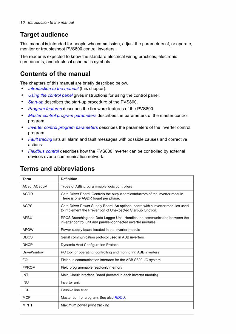
Terms and abbreviations
Term Definition
AC80, AC800M Types of ABB programmable logic controllers
AGDR Gate Driver Board. Controls the output semiconductors of the inverter module. There is one AGDR board per phase.
AGPS Gate Driver Power Supply Board. An optional board within inverter modules used to implement the Prevention of Unexpected Start-up function.
APBU PPCS Branching and Data Logger Unit. Handles the communication between the inverter control unit and parallel-connected inverter modules.
APOW Power supply board located in the inverter module
DDCS Serial communication protocol used in ABB inverters
DHCP Dynamic Host Configuration Protocol
DriveWindow PC tool for operating, controlling and monitoring ABB inverters
FCI Fieldbus communication interface for the ABB S800 I/O system
FPROM Field programmable read-only memory
INT Main Circuit Interface Board (located in each inverter module)
INU Inverter unit
LCL Passive line filter
MCP Master control program. See also RDCU.
MPPT Maximum power point tracking

Introduction to the manual 11
NAMU Auxiliary measuring unit
NDBU DDCS branching unit
NETA Ethernet adapter module (optional)
PGND board Grounding monitoring board
RAIO Analog I/O extension module (optional)
RAM Random-access memory
RDCO DDCS Communication Option; a satellite board that can be snapped on the RMIO board to add the number of fiber optic channels available
RDCU Type of control unit. The PVS800 contains two RDCUs. One of the RDCUs [A41] controls the inverter unit, the other [A43] contains the master control program. The RDCU houses the RMIO board.
RDIO Digital I/O extension module (optional)
RDNA DeviceNet adapter module (optional)
RETA Ethernet and Modbus TCP adapter module (optional)
RMBA Modbus adapter module (optional)
RMIO Control and I/O board contained within the RDCU
RPBA PROFIBUS adapter module (optional)
Term Definition

12 Introduction to the manual

Using the control panel 13
2
Using the control panel
What this chapter containsThis chapter describes how to use the control panel CDP 312R.
GeneralThe control panel can be used to control the PVS800 central inverter, read status data, and adjust parameters. The inverter is programmable through a set of parameters.
The communication between the CDP 312R control panel and the inverter uses the Modbus protocol. The communication speed of the bus is 9600 bit/s. You can connect 31 stations (inverters, drives, etc.) and one panel to the bus. Each station must have a unique ID number.

14 Using the control panel
Overview of the panel
Identification display
When the control panel is connected to the panel link for the first time, or when the inverter is powered up, the identification display shows the panel software version:
After the identification display, the panel enters the Control Unit Selection mode and displays the following program information:
After a few seconds, the display is cleared, and the Actual Signal Display mode appears.
1 L -> 795.0 VSTATE STAND BYPOWER 0 kWCURRENT 0 A
ACT PAR FUNC DRIVE
ENTER
LOC RESET REF
REM
I 0
134
2
The LCD type display has four lines of 20 characters.
The language is selected at start-up. The control panel has four operation modes:
• Actual Signal Display mode (ACT key)
• Parameter mode (PAR key)
• Function mode (FUNC key)
• Control Unit Selection mode (DRIVE key)
The use of single arrow keys, double arrow keys and ENTER depend on the operation mode of the panel.
The control keys are:
No. Used to 1 Start2 Stop3 Fault reset4 Change between Local/Remote (external)
control
CDP312 PANEL V5.30
PVS800 PVA
ID-NUMBER 1GSXR7400

Using the control panel 15
Panel operation mode keys and displays
The control panel keys allow you to select status data, parameters and change parameter settings. The figure below shows the mode selection keys of the panel, and the basic operations and displays in each mode.
Status row
The figure below describes the status row digits.
Parameter mode
Function mode
Control Unit Selection mode
Act. signal / Fault history
Enter selection modeAccept new signal
Group selection
Parameter selection
Enter change modeAccept new value
Fast value change
Slow value change
Function start
Control unit selection
Enter change modeAccept new value
Actual Signal Display mode
ENTER
ENTER
ENTER
ENTER
selection
ID number change
Status row
Status row
ACT
PAR
FUNC
DRIVE
1 L -> 795.0 VSTATE STAND BYAC POWER 0AC CURR 0
1 L -> 795.0 V99 START-UP DATA01 LANGUAGE ENGLISH
1 L -> 795.0 VUPLOAD <= <=DOWNLOAD CONTRAST 4
PVS800 PVA
GSXR7400ID-NUMBER 1
Act. signal / Fault message scrolling
Actual signal names and values
Parameter group
Parameter
Parameter value
Status row
List of functions
Device type
Program version and ID number
Row selection
Page selection => =>
Control unit ID number
Control statusL = Local control
“ “ = External control
StatusI = RunningO = Stopped“ “ = Run disabled
1 L -> 795.0 V I
Direction of power flow
<- = From inverter togrid
Measured DC voltage
16 Using the control panel
PVS800 control with the panelYou can use the panel to:• start and stop the PVS800
• reset any fault and alarm messages
• change between local and external control locations.
The panel can be used for PVS800 control only when the PVS800 is under local control and the status row is visible on the display. • L indicates local control on the panel display
• A blank space in the same location indicates external control (through I/O or fieldbus interface).
Remote control allows the following controls:• Monitoring actual signals
• Setting parameters
• Uploading parameters
• Setting ID number.
Note: Operational commands (eg, start/stop) cannot be given from the panel when the PVS800 is in remote control.
Control units of the PVS800
The PVS800 central inverter contains two control units: • Master control unit (running the master control program)
• Inverter control unit (running the inverter control program).
The control panel is wired to both control units through a Y-splitter.
The PVS800 can be configured and monitored through the master control program (by default, ID 1). To access the parameters and alarm/fault information of the inverter control program, see Control Unit Selection mode on page 23 for instructions on how to switch the panel between the control units.
How to start and stop the PVS800
Step Action Press Key Display
1. To show the status row. 1 -> 795.0 VSTATE STAND BYAC POWER 0AC CURR 0
2. To switch to local control.(Only if the PVS800 is not in local control already, ie, if there is no L on the first row of the display.)
Note: Switching to local control can be prevented by parameter 16.04 LOCAL LOCK.See page 70.
1 L -> 795.0 VSTATE STAND BYAC POWER 0AC CURR 0
3. To stop. 1 L -> 795.0 VSTATE STAND BYAC POWER 0AC CURR 0
4. To start. 1 L <- 795.0 V ISTATE SLEEPAC POWER 0AC CURR 0
ACT
LOC
REM

Using the control panel 17
Actual Signal Display modeThe Actual Signal Display mode includes two displays: the Actual Signal Display and the Fault History Display.
In this mode, you can:• view three actual signals on the display at a time
• select the actual signals to be displayed
• view the fault history
• reset the fault history.
The panel enters the Actual Signal Display mode by pressing the ACT key, or if no key is pressed within one minute. If a fault is active, the panel shows the Fault History Display before the panel enters the Actual Signal Display mode. If the Control Unit Selection mode is active, the panel shows the Status Display of the Control Unit Selection mode.
How to select the actual signals for display
Step Action Press key Display
1. To enter the Actual Signal Display mode. 1 L -> 795.0 VSTATE STAND BYAC POWER 0AC CURR 0
2. To select a row (a blinking cursor indicates the selected row).
1 L -> 795.0 VSTATE STAND BYAC POWER 0AC CURR 0
3. To enter the actual signal selection function. 1 L -> 795.0 V1 ACTUAL SIGNALS10 AC POWER [kW] 0
4. To select an actual signal.
To change the actual signal group.
1 L -> 795.0 V1 ACTUAL SIGNALS14 REACTIVE POWER 0
5. To accept the selection and to return to the Actual Signal Display mode.
1 L -> 795.0 VSTATE STAND BYREACTIVE 0AC CURRE 0
6. To cancel the selection and keep the original selection, press any of the mode selection keys.
The selected keypad mode is entered.
1 L -> 795.0 VSTATE STAND BYAC POWER 0AC CURR 0
ACT
ENTER
ENTER
ACT
FUNC DRIVE
PAR

18 Using the control panel
How to display the full name of actual signals
How to view and reset the fault history
Note: • Fault history cannot be reset if there are active faults or alarms.
• When viewing the fault history of master control program, fault and alarm messages generated by inverter control program are shown with a sign ”>” before the name of fault or alarm.
• More information on the fault/alarm is stored in the fault history of the inverter control program. To switch to the inverter control program and view its fault history, see How to select a control unit and change its panel link ID number on page 23. See also Fault history on page 48.
Step Action Press key Display
1. To display the full name of three actual signals. Hold 1 L -> 795.0 VPVA STATESAC POWER [kW]AC CURRENT L1
2. To return to the Actual Signal Display mode. Release 1 L -> 795.0 VSTATE STAND BYAC POWER 0AC CURR 0
Step Action Press key Display
1. To enter the Actual Signal Display mode. 1 L -> 795.0 VSTATE STAND BYAC POWER 0AC CURR 0
2. To enter the Fault History Display. 1 L -> 795.0 V 2 LAST FAULT -PANEL LOST (5300) 20 H 49 MIN 56 S
3. To select the previous (UP) or the next fault/alarm (DOWN).
1 L -> 795.0 V 2 LAST FAULT H MIN S
To clear the Fault History. 1 L -> 795.0 V 2 LAST FAULT +SYSTEM START (1087) 12 H 49 MIN 10 S
4. To return to the Actual Signal Display mode. 1 L -> 795.0 VSTATE STAND BYAC POWER 0AC CURR 0
ACT
ACT
ACT
RESET

Using the control panel 19
About the fault history
The fault history restores information on the 16 latest events (faults, alarms and resets) of the control program. The table below shows how the events are stored in the fault history.
How to display and reset an active fault
Step Action Press Key Display
1. To display an active fault. 1 L -> 795.0 VPVS800 PVA*** FAULT ***PANEL LOSS (5300)
2. To reset the fault. 1 L -> 795.0 VSTATE STAND BYAC POWER 0AC CURRE 0
1 L -> 795.0 V 2 LAST FAULT-PANEL LOST (5300) 12 H 49 MIN 10 S
Event Information on display
PVS800 detects a fault and generates a fault message.
Sequential number of the event and LAST FAULT text
Name of the fault and a “+” sign in front of the name
Total power-on time
User resets the fault message.
Sequential number of the event and LAST FAULT text
RESET FAULT text
Total power-on time
PVS800 generates an alarm message.
Sequential number of the event and LAST WARNING text
Name of the alarm and a “+” sign in front of the name
Total power-on time
PVS800 deactivates the alarm message.
Sequential number of the event and LAST WARNING text
Name of the alarm and a “-” sign in front of the name
Total power-on time
Sequential number (1 is the most recent event)
Sign
Power-
on time
Name andcode
A Fault History View
ACT
RESET
20 Using the control panel
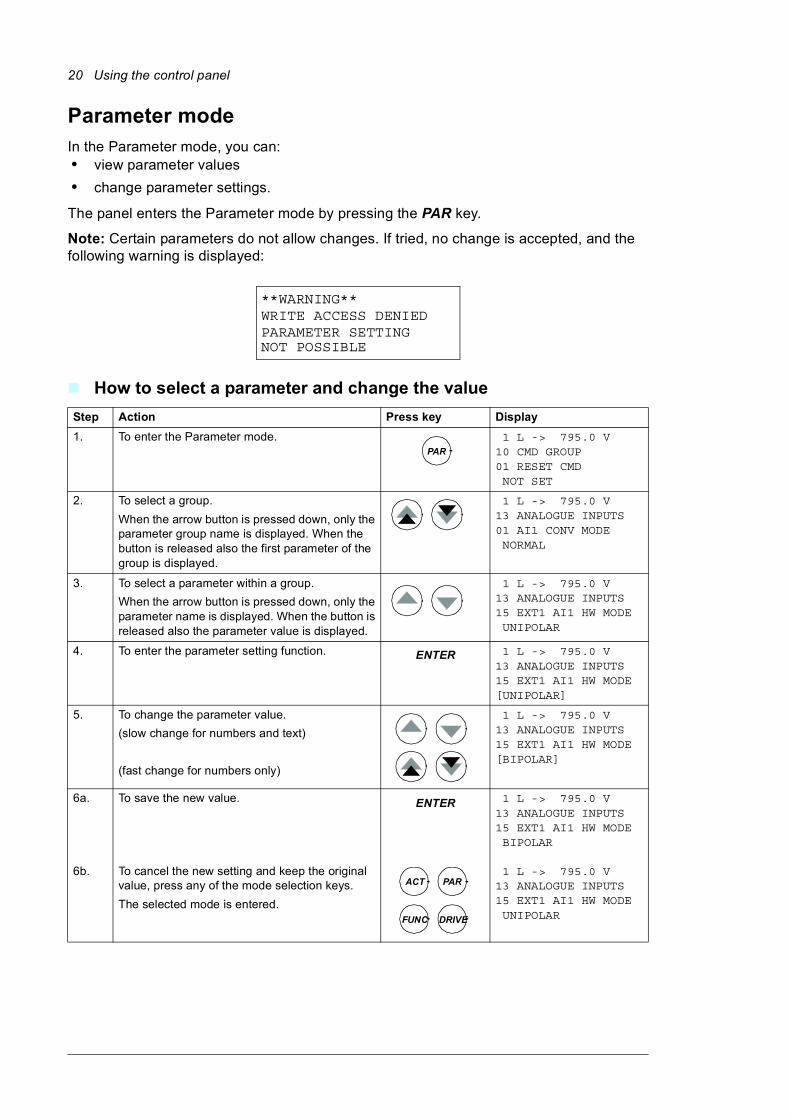
Parameter modeIn the Parameter mode, you can:• view parameter values
• change parameter settings.
The panel enters the Parameter mode by pressing the PAR key.
Note: Certain parameters do not allow changes. If tried, no change is accepted, and the following warning is displayed:
How to select a parameter and change the value
Step Action Press key Display
1. To enter the Parameter mode. 1 L -> 795.0 V10 CMD GROUP01 RESET CMD NOT SET
2. To select a group.
When the arrow button is pressed down, only the parameter group name is displayed. When the button is released also the first parameter of the group is displayed.
1 L -> 795.0 V13 ANALOGUE INPUTS01 AI1 CONV MODE NORMAL
3. To select a parameter within a group.
When the arrow button is pressed down, only the parameter name is displayed. When the button is released also the parameter value is displayed.
1 L -> 795.0 V13 ANALOGUE INPUTS15 EXT1 AI1 HW MODE UNIPOLAR
4. To enter the parameter setting function. 1 L -> 795.0 V13 ANALOGUE INPUTS15 EXT1 AI1 HW MODE[UNIPOLAR]
5. To change the parameter value.
(slow change for numbers and text)
(fast change for numbers only)
1 L -> 795.0 V13 ANALOGUE INPUTS15 EXT1 AI1 HW MODE[BIPOLAR]
6a. To save the new value. 1 L -> 795.0 V13 ANALOGUE INPUTS15 EXT1 AI1 HW MODE BIPOLAR
6b. To cancel the new setting and keep the original value, press any of the mode selection keys.
The selected mode is entered.
1 L -> 795.0 V13 ANALOGUE INPUTS15 EXT1 AI1 HW MODE UNIPOLAR
**WARNING**
NOT POSSIBLE
WRITE ACCESS DENIEDPARAMETER SETTING
PAR
ENTER
ENTER
ACT
FUNC DRIVE
PAR

Using the control panel 21
How to adjust a source selection parameter
The value in most of the parameters is used directly in the control program. The source selection parameters are an exception because the values point to another parameter whose values are used in the control program. Therefore, the procedure to set source selection parameters differs from that of other parameters.
1)
Note: Instead of pointing to another parameter, it is also possible to define a constant by the source selection parameter. Proceed as follows:
1. Change the inversion field to C.
The appearance of the row changes. The rest of the lines is now a constant setting field.
2. Give the constant value to the constant setting field.
3. Press ENTER to accept.
Step Action Press Key Display
1. See the table above to
• enter the Parameter mode
• select the correct parameter group and parameter
• enter the parameter setting mode.
1 L -> 795.0 V55 ADAPTIVE PROG106 INPUT1 +.000.000.00
2. To scroll between the inversion, group, index and bit fields.1)
1 L -> 795.0 V55 ADAPTIVE PROG106 INPUT1[±.000.000.00]
3. To adjust the value of a field. 1 L -> 795.0 V55 ADAPTIVE PROG106 INPUT1[±.000.018.00]
4. To accept the value. 1 L -> 795.0 V55 ADAPTIVE PROG106 INPUT1 +.000.018.00
PAR
ENTER
ENTER
1 L -> 795.0 V55 ADAPTIVE PROG1xxx06 INPUT1[±.001.018.00]
Inversion fieldGroup fieldIndex field
Bit field
Inversion field inverts the selected parameter value. Plus sign (+): no inversion, minus (-) sign: inversion.
Bit field selects the bit number (relevant only if the parameter value is a packed Boolean word).
Index field selects the parameter index.
Group field selects the parameter group.
22 Using the control panel
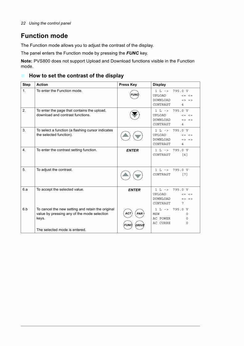
Function modeThe Function mode allows you to adjust the contrast of the display.
The panel enters the Function mode by pressing the FUNC key.
Note: PVS800 does not support Upload and Download functions visible in the Function mode.
How to set the contrast of the display
Step Action Press Key Display
1. To enter the Function mode. 1 L -> 795.0 VUPLOAD <= <=DOWNLOAD => =>CONTRAST 4
2. To enter the page that contains the upload, download and contrast functions.
1 L -> 795.0 VUPLOAD <= <=DOWNLOAD => =>CONTRAST 4
3. To select a function (a flashing cursor indicates the selected function).
1 L -> 795.0 VUPLOAD <= <=DOWNLOAD => =>CONTRAST 4
4. To enter the contrast setting function. 1 L -> 795.0 VCONTRAST [4]
5. To adjust the contrast. 1 L -> 795.0 VCONTRAST [7]
6.a To accept the selected value. 1 L -> 795.0 VUPLOAD <= <=DOWNLOAD => =>CONTRAST 7
6.b To cancel the new setting and retain the original value by pressing any of the mode selection keys.
The selected mode is entered.
1 L -> 795.0 VMSW 0AC POWER 0AC CURRE 0
FUNC
ENTER
ENTER
ACT
FUNC DRIVE
PAR

Using the control panel 23
Control Unit Selection modeThe Control Unit Selection mode can be used to switch the control panel between master control unit and inverter control unit.
In the Control Unit Selection mode, it is possible to:• select the control unit (master or inverter) with which the control panel communicates
• change the identification number of a control unit
• view the status of the control units connected to the panel.
The panel enters the Control Unit Selection mode by pressing the DRIVE key.
Each on-line control unit must have an individual identification number (ID). By default,• the ID number of the master control unit (master control program) is 1
• the ID number of the inverter control unit (inverter control program) is 2.
Note: The default ID number settings of the two control units of the PVS800 should not be changed unless the PVS800 is to be connected to a panel link (constructed by using optional NBCI-xx modules) with other PVS800 inverters on-line.
How to select a control unit and change its panel link ID number
Step Action Press key Display
1. To enter the Control Unit Selection mode. PVS800 PVA
GSXR7400ID-NUMBER 1
2. To select the next control unit/view.
The ID number of the current control unit is changed by first pressing ENTER (the brackets round the ID number appear) and then adjusting the value with arrow buttons. The new value is accepted with ENTER. Switch off the power to the control unit, to validate its new ID number setting.
PVS800 xxxx_5PV
ISXR7400
ID-NUMBER 2
The status display of all devices connected to the Panel Link is shown after the last individual station. If all stations do not fit on the display at once, press the double-arrow up to view the rest of them.
Status Display Symbols: = Stopped
F = Tripped on a fault
3. To connect to the last displayed control unit and to enter another mode, press one of the mode selection keys.
The selected mode is entered.
DRIVE
1o
o
PAR
FUNC
ACT

24 Using the control panel
Reading and entering packed Boolean values on the displaySome actual values and parameters are packed Boolean, that is, each individual bit has a defined meaning (explained at the corresponding signal or parameter). On the control panel, packed Boolean values are read and entered in hexadecimal format.
In this example, bits 1, 3 and 4 of the packed Boolean value are On:
Boolean 0000 0000 0001 1010Hex 0 0 1 A
Bit 15 Bit 0

Start-up 25
3
Start-up
What this chapter containsThis chapter describes the start-up procedure of the PVS800 central inverter.
Start-up procedureUse local control when you start up the inverter.
Note: Keep in hand the grid specification from grid operator.
Description Comments
SAFETY
WARNING! Obey all safety instructions delivered with the inverter. See the hardware manual. Only qualified electricians are allowed to start-up the inverter.
PRIMARY CHECKS
Make sure that the mechanical and electrical installation and other preparations are made according to the instructions given in the hardware manual.
-
COMMISSIONING APBU
Set APBU battery dip switch (S3:6) from OFF to ON.
-Upload the available APBU logger data from user, last and first loggers from APBU to PC.

26 Start-up
START AND STOP SETTINGS
Adjust the start settings.
• 31.04 UDC START LIM (page 79). This value must be lower than the open-circuit voltage of the solar generator.
• 31.05 UDC START DLY (page 79). The correct setting minimizes the number of unnecessary starts during low light conditions.
0.9 × open circuit voltage is a good initial estimate for 31.04 UDC START LIM.
If necessary, adjust the stop settings.
• 31.07 UDC STOP DLY (page 80)
• 31.10 POWER STOP LIM (page 80)
• 31.11 POWER STOP DLY (page 80)
• 31.12 GOTO SLEEP MODE (page 80)
The default values are suitable for most installations.
Monitor the operation of the inverter and fine-tune the voltage levels and delays for optimal performance.
You must continue the monitoring for at least a couple of days.
AUTOMATIC FAULT RESET
If necessary, enable the automatic reset logic.
• 30.04 RESET DELAY [s] (page 78)
• 30.05 NUMBER OF TRIALS (page 78)
• 30.11 AUTO RESET MASK (page 79)
You are recommended to enable the automatic reset logic if the inverter is not controlled through the fieldbus interface.
GRID CONNECTION
Adjust the settings for Grid monitoring with parameters 44.02 OVER FREQ 1 LIM … 44.17 OVER VOLT 2 TIME (pages 157…158).
• Undervoltage
• Overvoltage
• Underfrequency
• Overfrequency
These settings are usually specified by the grid operator.
Adjust the settings for Cut-in condition checking with parameters 44.18 CUT-IN CHECK ENA … 44.23 CUT-IN DELAY (pages 159…159).
These settings define the voltage and frequency ranges where the inverter can start, as well as a connection delay.
These settings are usually specified by the grid operator.
ACTIVE POWER LIMITATION
Adjust the settings for Active power limitation from grid overfrequency with the following parameters.
• 42.07 P FREQ LIM ENA … 42.11 P LIMITING FREQ 3 (pages 153…154)
• 42.13 P(f) RETURN DELAY (page 154)
• 42.14 P(f) RETURN RAMP (page 154)
These settings are usually specified by the grid operator.
Adjust the settings for Active power limitation from grid overvoltage with parameters 42.20 UAC PLIM MODE SEL … 42.27 UAC PLIM LEVEL 2 (pages 155…156).
These settings are usually specified by the grid operator.
Adjust the settings for active power ramping after start with parameters with parameters 42.05 RESTR ACTPOW GRD1 (page 152) and 42.06 RESTR ACTPOW GRD2 (page 153).
These settings are usually specified by the grid operator.
Description Comments
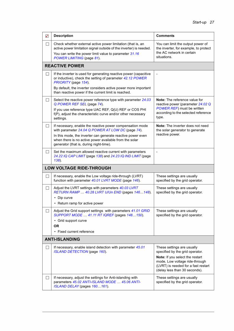
Start-up 27
Check whether external active power limitation (that is, an active power limitation signal outside of the inverter) is needed.
You can write the power limit value to parameter 31.16 POWER LIMITING (page 81).
You can limit the output power of the inverter, for example, to protect the AC network in certain situations.
REACTIVE POWER
If the inverter is used for generating reactive power (capacitive or inductive), check the setting of parameter 42.12 POWER PRIORITY (page 154).
By default, the inverter considers active power more important than reactive power if the current limit is reached.
-
Select the reactive power reference type with parameter 24.03 Q POWER REF SEL (page 74).
If you use reference type UAC REF, Q(U) REF or COS PHI f(P), adjust the characteristic curve and/or other necessary settings.
Note: The reference value for reactive power (parameter 24.02 Q POWER REF) must be written according to the selected reference type.
If necessary, enable the reactive power compensation mode with parameter 24.04 Q POWER AT LOW DC (page 74).
In this mode, the inverter can generate reactive power even when there is no active power available from the solar generator (that is, during night-time).
Note: The inverter does not need the solar generator to generate reactive power.
Set the maximum allowed reactive current with parameters 24.22 IQ CAP LIMIT (page 138) and 24.23 IQ IND LIMIT (page 138).
-
LOW VOLTAGE RIDE-THROUGH
If necessary, enable the Low voltage ride-through (LVRT) function with parameter 40.01 LVRT MODE (page 146).
These settings are usually specified by the grid operator.
Adjust the LVRT settings with parameters 40.03 LVRT RETURN RAMP … 40.28 LVRT U/Un END (pages 146…148).
• Dip curve
• Return ramp for active power
These settings are usually specified by the grid operator.
Adjust the Grid support settings with parameters 41.01 GRID SUPPORT MODE … 41.11 RT IQREF (pages 148…150).
• Grid support curve
OR
• Fixed current reference
These settings are usually specified by the grid operator.
ANTI-ISLANDING
If necessary, enable island detection with parameter 45.01 ISLAND DETECTION (page 160).
These settings are usually specified by the grid operator.
Note: If you select the restart mode, Low voltage ride-through (LVRT) is needed for a fast restart (delay less than 30 seconds).
If necessary, adjust the settings for Anti-islanding with parameters 45.02 ANTI-ISLAND MODE … 45.06 ANTI-ISLAND DELAY (pages 160…161).
These settings are usually specified by the grid operator.
Description Comments

28 Start-up
CONNECTION TO THE REMOTE SYSTEM
If the inverter is equipped with the NETA-01 Ethernet adapter module, and the module is used for transmitting data to the remote monitoring portal, configure the remote monitoring according to ABB Remote monitoring portal user's manual (3AUA0000098904 [English]).
-
AUTOMATIC START
If you want the inverter to start automatically after an auxiliary power loss, configure the automatic start functionality.
Note: If automatic start is in use, the inverter will start even if the start button has not been pressed on the control panel.
Description Comments

Program features 29
4
Program features
What this chapter containsThis chapter describes the program features of the PVS800 central inverter. For each feature, there is a list of related parameters, faults and alarms if applicable.

30 Program features
Control interfaces
Local vs. External control
The PVS800 central inverter can be controlled/monitored:• locally from control panel
• locally from DriveWindow PC tool (connect the fibre optic cables to DDCS channel CH3 on the RDCO DDCS Communication Option module)
• externally through I/O and/or the fieldbus interface.
With control panel or DriveWindow PC tool, the user can change parameters, view/reset the fault history, and stop the inverter.
Control panel
Both control units of the PVS800 can be monitored and controlled locally from a single CDP 312R control panel. Most of the essential functions (start, stop, fault reset, etc.) of the inverter are available through the master control program. In case the parameters, fault history, etc. of the inverter unit must be accessed, select control unit ID 2 in Control Unit Selection mode (see page 23).
DriveWindow
DriveWindow and other tools can be connected to DDCS channel CH3 on the master control unit (RDCU, designation A43), either in a ring or a star configuration using NDBU branching units. With multiple inverters, different node numbers must be set for each inverter before starting the communication (see parameter 70.15 CH3 NODE ADDR, page 106). This setting can be made with control panel CDP 312R or by a point-to-point connection with DriveWindow. The new node address becomes valid on the next power-up of the control unit.
Fieldbus
For information on how to control/monitor the PVS800 through an external control system, see chapter Fieldbus control (page 197).
I/O
The PVS800 can be controlled and monitored with digital and analog signals connected to the master control unit. See the hardware manual for the available connections. See also section Automatic fault reset (page 47).

Program features 31
PVS800 state machineThe PVS800 follows the state machine shown below.
The following table describes the PVS800 machine states. The required signals are shown in the table describing the conditions of state transitions.
State Description
STANDBY The inverter is powered and it is waiting for a start command. The power-up initialization routine is performed and the inverter unit is ready. There are no active faults. The DC and AC contactors are open.
SLEEP The start command is active but the inverter is waiting for all start conditions to be filled. The start conditions includes a sufficient DC voltage level and corresponding time delay as well as wake up signals.
START ISU The start command is active and all start conditions are met. The start command is sent to the inverter unit and the cut-in procedure is activated. The inverter synchronizes and connects to the grid if all required conditions are fulfilled. After the grid connection, the DC contactors will be closed.
MPPT The maximum power point tracker (MPPT) state is the normal operation state of the PVS800 when the inverter is feeding power to the grid. The inverter is producing maximal power under available conditions.
1STAND BY
2SLEEP
3START ISU
4MPPT
5ISU LOCAL
6FAULTED
7Q POWER
FROM ALL STATES
FROM ALL STATES
L
A
B1
B2
CD
E
F
G
HI
J
K
OP
QR
S
M
N
T
U
V

32 Program features
The conditions for state transitions are as follows:
ISU LOCAL The inverter control unit is switched to the local control mode. This mode can be used, eg, for testing and commissioning purposes even without the DC power. For more information about the ISU local mode, see section Starting the inverter unit without solar generator power on page 34.
FAULTED The PVS800 is set to the faulted state when a fault occurs in the master control program or in the inverter control program. The inverter is stopped and AC and DC contactors are opened.
Q POWER Reactive power compensation mode is activated, the start command is active and the inverter is waiting for all start conditions to be met. In this state, reactive power can be generated with the DC contactor open. The inverter stays running until the reactive power reference falls below a certain level for a certain time delay. The inverter is then stopped and the AC contactor opened. When the reactive power reference reaches the same level again, the AC contactor is closed and the inverter started again.
A 08.05 PVA STATUS WORD bit 1 = 1
B1 08.05 PVA STATUS WORD bit 1 = 0 AND UDC > 31.04 UDC START LIM AND start command ON
B2 08.05 PVA STATUS WORD bit 1 = 0 AND UDC < 31.04 UDC START LIM AND start command ON
AND 24.04 Q POWER AT LOW DC = OFF
C Start command ON AND 08.05 PVA STATUS WORD bit 3 = 1 AND 31.01 ENABLE MPPT = 1 AND 24.04 Q POWER AT LOW DC = OFF
D Start command removed OR 08.05 PVA STATUS WORD bit 3 = 0 OR 31.01 ENABLE MPPT = 0
E UDC > 31.04 UDC START LIM AND 31.05 UDC START DLY elapsed AND 31.13 WAKE UP
SOURCE > 31.14 WAKE UP START LIM AND 31.15 WAKE UP START DLY elapsed AND 08.07 GND STATUS WORD bit 2 = 1
F UDC < 31.06 UDC STOP LIM AND 31.07 UDC STOP DLY elapsed AND 24.04 Q POWER AT LOW
DC = OFF
G Start command removed OR 08.05 PVA STATUS WORD bit 3 = 0 OR 31.01 ENABLE MPPT = 0
H 08.05 PVA STATUS WORD bit 0 = 1
I 08.05 PVA STATUS WORD bit 0 = 0
J (UDC < 31.06 UDC STOP LIM AND 31.07 UDC STOP DLY elapsed) OR
(31.09 POWER SOURCE < 31.10 POWER STOP LIM AND 31.11 POWER STOP DLY elapsed) AND 24.04 Q POWER AT LOW DC = OFF
K Start command removed OR 31.01 ENABLE MPPT = 0 OR 08.05 PVA STATUS WORD bit 3 = 0
L A fault occurred. Exception: From the ISU LOCAL mode, the inverter is not set to the FAULTED state even if a fault occurs.
M Reset command was given
N 08.05 PVA STATUS WORD bit 1 = 0 AND start command OFF
O 24.04 Q POWER AT LOW DC = ON
P 24.04 Q POWER AT LOW DC = OFF
Q UDC > 31.04 UDC START LIM AND 31.05 UDC START DLY elapsed AND 31.13 WAKE UP
SOURCE > 31.14 WAKE UP START LIM AND 31.15 WAKE UP START DLY elapsed AND 08.07 GND STATUS WORD bit 2 = 1
State Description

Program features 33
The parameters above are described in chapter Master control program parameters.
R UDC < 31.06 UDC STOP LIM AND 31.07 UDC STOP DLY elapsed AND 24.04 Q POWER AT LOW
DC = ON
S (UDC < 31.06 UDC STOP LIM AND 31.07 UDC STOP DLY elapsed) OR
(31.09 POWER SOURCE < 31.10 POWER STOP LIM AND 31.11 POWER STOP DLY elapsed) AND 24.04 Q POWER AT LOW DC = ON
T Start command ON AND 24.04 Q POWER AT LOW DC = ON AND08.05 PVA STATUS WORD bit 3 = 1 AND 31.01 ENABLE MPPT = 1
U Start command OFF OR 08.05 PVA STATUS WORD bit 3 = 0 OR 31.01 ENABLE MPPT = 0
V 08.05 PVA STATUS WORD bit 1 = 0 AND UDC < 31.04 UDC START LIM AND start command ON
AND 24.04 Q POWER AT LOW DC = ON

34 Program features
Maximum power point tracking (MPPT)The maximum power point of a solar panel refers to the point on the output current/voltage curve where the product of current and voltage is at maximum. The current and voltage are dependent on solar radiation and panel temperature, so the maximum power point may move on the curve. There may even be multiple maximum points.
The internal Maximum power point tracking (MPPT) function of the PVS800 automatically operates the solar panels at their maximum power point under all conditions.
External MPPT reference
In normal use, the internal MPPT algorithm provides the PVS800 with a DC reference. An external DC reference can alternatively be used if necessary.
Settings
Inverter control program: Parameter group 39 MPPT CONTROL (page 145)
Diagnostics
Master control program: Parameters 08.04 PVA STATES (page 58) and 08.05 PVA STATUS WORD (page 59)
Operation voltagesThe normal operation range of the maximum power point tracking (MPPT) depends on the inverter nominal power according to the table below.
Starting the inverter unit without solar generator powerThe inverter unit of the PVS800 can be started in local control with the solar generator disconnected (with DC contactor open) as long as the inverter is connected to the grid. This special mode can be used for testing during commissioning or troubleshooting. In this mode the inverter does not produce active power.
In the ISU local mode the inverter can be run without solar modules connected to the inverter, for example, to test the start-up procedure in an existing AC grid. DC contactors are not closed in the ISU LOCAL mode.
Settings
• To switch control to the inverter control program, see instructions in Control Unit Selection mode on page 23.
• To switch to the local control mode and start the inverter, see instructions in How to start and stop the PVS800 on page 16.
Inverter power MPPT range
100 kW, 250 kW, 500 kW 450…825 V
315 kW, 630 kW, 875 kW 525…825 V
1000 kW 600…850 V
Program features 35
Grid identificationAt first start, the inverter unit adapts itself to the grid automatically. No grid data needs to be set by the user.
During identification, the grid voltage, frequency and phase order are recognized. This takes approximately four seconds.
Automatic grid identification is active by default. This means that the grid identification is repeated every time when the PVS800 is started after a break in the auxiliary power supply. Automatic grid identification can be deactivated with parameter 99.08 AUTO LINE ID RUN (page 175) if the grid identification is successfully completed during commissioning. Manual grid identification can also be chosen.
Settings
Inverter control program: Parameters 99.07 LINE SIDE ID RUN (page 174) and 99.08 AUTO LINE ID RUN (page 175)
Diagnostics
• Master control program: Parameter 09.11 SUPPLY FAULT WORD, bit 9 (page 60)
• Fault >NET VOLT (3285) (page 183)
Cut-in condition checkingIn some grid codes it is required that the grid is normal for a specified time before the inverter can start. The PVS800 can be set to perform a cut-in condition (that is, start condition) check for the grid based on measurements from the NAMU board. The check makes sure that the inverter will not start until the grid frequency and voltage are within pre-defined limits for longer than an adjustable delay.
If other start conditions (for example, the DC voltage) give a permission to start, but the cut-in condition check fails, the inverter generates an alarm.
Settings
Inverter control program: Parameters 44.18 CUT-IN CHECK ENA … 44.23 CUT-IN DELAY (pages 159…159)
Diagnostics
Alarm >RUN DISABLE (8194) (page 184)
DC overvoltage monitoringThe PVS800 will not start if the measured DC voltage exceeds an internal start limit (1000 V by default). The voltage must remain below the limit for 60 seconds before the inverter can start.
If the DC voltage exceeds an internal limit (900 V by default) while the inverter is running in the MPPT mode, the inverter will go to Sleep mode. This may be caused by active power limitation or incorrect solar array sizing.
Diagnostics
• Master control program: Parameter 09.15 PVA ALARM WORD, bit 6 (page 62)
• Alarm UDC HIGH LIM (32A7) (page 184)

36 Program features
Automatic start after a power-upThe PVS800 can be set to start automatically after the auxiliary power to the control units is switched on. This enables the PVS800 to start after a power failure without the need of an operator locally pressing the Start button.
To use this functionality, I/O control must be enabled (10.02 ENABLE I/O CTRL, page 64). If a constant start command is selected by parameter 10.04 I/O START SOURCE (page 64), the PVS800 will start automatically after the auxiliary power is switched On. The default input for the Start/Stop signal is digital input DI2 on the master control unit [A43]. A constant value 1 can be selected by setting parameter 10.04 I/O START SOURCE to C.00001. Note that a wire connection to DI2 is not needed.
If the PVS800 is equipped with an emergency stop relay (option +Q951), it must be acknowledged before the Start command is accepted. This can be done with a relay output on the master control unit (see parameter 10.03 EM STOP AUTORESET, page 64 and the hardware manual).
WARNING! If I/O control is enabled and a Start command is active, the PVS800 will start after the auxiliary power to the control units is switched On.
Settings
Master control program: Parameters 10.02 ENABLE I/O CTRL … 10.05 I/O RESET SOURCE (page 64)
Diagnostics
Alarm IO START ENA (61AA) (page 182)
Reactive power controlThe PVS800 is capable of generating a selectable amount of reactive power to the grid (positive = capacitive, negative = inductive). A reference value for the reactive power can be given through the CDP312R control panel, PC tools, fieldbuses or PLC. Other inputs (like analog and digital inputs) can be used with an adaptive program.
A reference type for the reactive power can be selected from eight different formats, see parameter 24.03 Q POWER REF SEL (page 74). A reference value must be finally written to a parameter 24.02 Q POWER REF (page 72) according to the selected reference format. Minimum limits for the reactive power reference are available in parameters 24.08 COS PHI CAP LIMIT and 24.09 COS PHI IND LIMIT (page 137).
Note: The PVS800 can generate reactive power according to the given reference if the current limit of the inverter is not exceeded. If the PVS800 is already feeding maximum allowed current to the grid, parameter 42.12 POWER PRIORITY defines if active or reactive power is limited. In this case the actual reactive power and the reactive power reference may not be the same.
See also section Operation voltages on page 34.
Settings
• Master control program: Parameter group 24 REACTIVE POWER (page 72)
• Inverter control program: Parameters 24.08 COS PHI CAP LIMIT (page 137), 24.09 COS PHI IND LIMIT (page 137) and 42.12 POWER PRIORITY (page 154)

Program features 37
Diagnostics
Master control program: Parameter 01.14 REACTIVE POWER (page 51)
Reactive power compensation
The PVS800 can be used for reactive power compensation even if the inverter is not producing active power. Reactive power compensation can be done without any power from the solar generator.
When the reactive power compensation mode is activated with parameter 24.04 Q POWER AT LOW DC (page 74), the inverter always goes to the Q POWER state instead of the SLEEP state when low DC voltage or output power is available in the evening. In the Q POWER state, the DC contactor is always open. The inverter stays running until the reactive power reference falls below the level defined by parameter 24.06 Q POW ZERO MARGIN (page 137) for the time defined by 24.05 Q POWER STOP DLY (page 137). The inverter is then stopped and the AC contactor opened. When the reactive power reference reaches the zero margin again, the AC contactor is closed and the inverter started again.
Transition actions to the reactive power compensation mode and MPPT mode are automatic and based on normal starting and stopping triggers, such as the DC voltage and output power level. Reactive power generation is not stopped during the transition actions. In the reactive power compensation mode, the inverter uses the same reactive power reference as in the MPPT mode.
See also section PVS800 state machine (page 31).
Settings
• Master control program: Parameters 24.02 Q POWER REF (page 72), 24.03 Q POWER REF SEL (page 74) and 24.04 Q POWER AT LOW DC (page 74)
• Inverter control program: Parameters 24.05 Q POWER STOP DLY (page 137) and 24.06 Q POW ZERO MARGIN (page 137)
Diagnostics
• Master control program: Parameters 01.14 REACTIVE POWER (page 51) and 08.04 PVA STATES (page 58)
• Inverter control program: Parameters 07.01 MAIN CTRL WORD, bit 4 (page 120) and 08.06 MPPT STATUS bit 14 (page 123)

38 Program features
Active power limitationThe active output power of the PVS800 can be limited using an external source (for example, through the grid operator). The power limitation signal can be directly sent to the PVS800 via the CDP312R control panel, PC tools, fieldbuses or PLC. Other inputs like analog and digital inputs can be used with an adaptive program.
A limitation signal for the active power must be written to parameter 31.16 POWER LIMITING (page 81). There is a ramping for the active power limitation (by default, a 10-second ramp if there is a stepwise change of 100% in the limitation signal).
An active power limitation is indicated by 08.08 LIMIT WORD (page 60). The active power can also be limited by the inverter itself. This may happen, for example, if the ambient temperature exceeds limits or if the reactive power is prioritized and the inverter current limit is reached.
Settings
Master control program: Parameters 31.16 POWER LIMITING (page 81)
Inverter control program: Parameters 42.12 POWER PRIORITY (page 154) and 90.04 D SET 12 VAL 1 (page 108)
Diagnostics
Master control program: Parameter 08.08 LIMIT WORD (page 60)
Active power limitation from grid overfrequency
In some grid codes and standards it is required that active power is limited as the grid frequency increases. The PVS800 has an adjustable active power limitation based on the measured grid frequency. The active power limitation curve can be of two types: incremental or free-running.
The diagram below shows an example of the incremental curve.
Active power level before limitation
42.10 P FREQ LIMIT 2
42.09 P LIMITING FREQ 2
02.18 GRID FREQUENCY
42.11 P LIMITING FREQ 3
PLIM
42.08 P LIMITING FREQ 1
Active limited power increases with a ramp rate defined by 42.14 P(f) RETURN RAMP.

Program features 39
The diagram below shows an example of the free-running curve.
Settings
Inverter control program: Parameters 42.07 P FREQ LIM ENA … 42.11 P LIMITING FREQ 3 (pages 153…154), 42.13 P(f) RETURN DELAY (page 154) and 42.14 P(f) RETURN RAMP (page 154)
Diagnostics
Inverter control program: 08.03 LIMIT WORD (page 122)
Active power limitation during grid underfrequency
In some grid codes and standards it is required that the maximum active output power of the inverter is increased as the grid frequency decreases. The PVS800 has an adjustable active power limitation curve based on the measured grid frequency.
The active power limit starts to increase when the grid frequency is below 46.05 UF PLIM FREQ 1 as shown in the figure below. The active power limit cannot decrease while the grid underfrequency situation is ongoing. As the grid frequency returns to a normal level defined by parameter 46.04 UF PLIM RET FREQ, the active power limit is ramped down to the level defined by parameter 46.06 UF PLIM LEVEL 1.
Active power level before limitation
42.10 P FREQ LIMIT 2
42.09 P LIMITING FREQ 2
02.18 GRID FREQUENCY
PLIM
42.08 P LIMITING FREQ 1
Active power limit
46.08 UF PLIM LEVEL 2
46.04 UF PLIM RET FREQ
46.07 UF PLIM FREQ 2
46.05 UF PLIM FREQ 1
46.06 UF PLIM LEVEL 1
02.18 GRID FREQUENCY
Active limited power decreases with ramp rate defined by 46.03 UF PLIM RET RAMP
40 Program features
Settings
Inverter control program: Parameters 46.01 UF PLIM MODE SEL (page 162) … 46.08 UF PLIM LEVEL 2 (page 162)
Diagnostics
Inverter control program: Parameters 08.03 LIMIT WORD (page 122) and 08.07 GRID CODE STATUS (page 123)
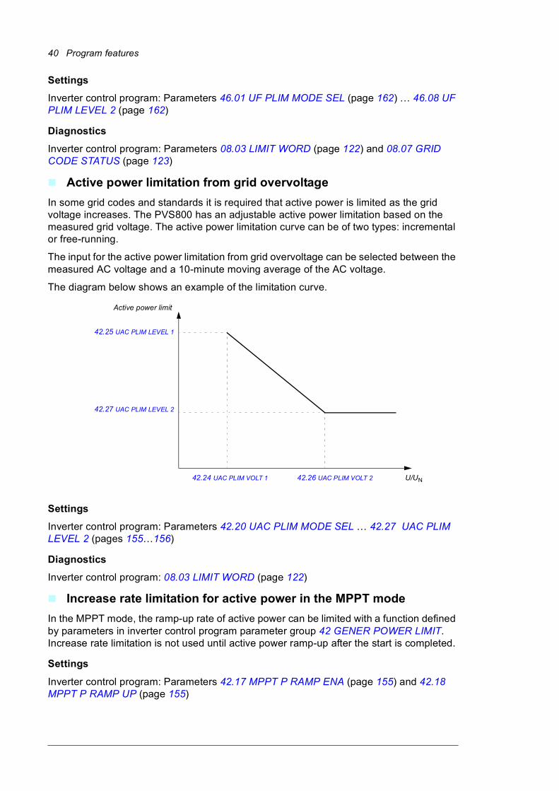
Active power limitation from grid overvoltage
In some grid codes and standards it is required that active power is limited as the grid voltage increases. The PVS800 has an adjustable active power limitation based on the measured grid voltage. The active power limitation curve can be of two types: incremental or free-running.
The input for the active power limitation from grid overvoltage can be selected between the measured AC voltage and a 10-minute moving average of the AC voltage.
The diagram below shows an example of the limitation curve.
Settings
Inverter control program: Parameters 42.20 UAC PLIM MODE SEL … 42.27 UAC PLIM LEVEL 2 (pages 155…156)
Diagnostics
Inverter control program: 08.03 LIMIT WORD (page 122)
Increase rate limitation for active power in the MPPT mode
In the MPPT mode, the ramp-up rate of active power can be limited with a function defined by parameters in inverter control program parameter group 42 GENER POWER LIMIT. Increase rate limitation is not used until active power ramp-up after the start is completed.
Settings
Inverter control program: Parameters 42.17 MPPT P RAMP ENA (page 155) and 42.18 MPPT P RAMP UP (page 155)
Active power limit
U/UN
42.25 UAC PLIM LEVEL 1
42.27 UAC PLIM LEVEL 2
42.24 UAC PLIM VOLT 1 42.26 UAC PLIM VOLT 2

Program features 41
Diagnostics
Inverter control program: Parameter 08.03 LIMIT WORD (page 122)
Active power ramp-up after a grid fault
If the PVS800 ends up with a grid fault and a new start is made after a fault reset, it is possible to limit active power with a ramp. When a fault is cleared by resetting and the PVS800 is started up again, the active power is increased with a ramp rate defined by parameter 42.05 RESTR ACTPOW GRD1 (page 152).
Grid faults are LVRT faults, external grid monitoring faults and NAMU grid monitoring faults. These faults are listed below:
Parameter 42.06 RESTR ACTPOW GRD2 (page 153) can be used if active power must be ramped up after other faults or after a stop.
Settings
• Inverter control program parameter for active power ramp-up when the PVS800 is started up after a grid fault: 42.05 RESTR ACTPOW GRD1 (page 152)
• Inverter control program parameter for active power ramp-up when the PVS800 is started up after other faults or a stop: 42.06 RESTR ACTPOW GRD2 (page 153)
Sleep modeThe PVS800 can be set to automatically go into sleep mode as the DC output voltage of the solar panels and/or output power of the inverter falls below a specified limit in the evening. The inverter disconnects from the grid, but the PVS800 still monitors the output of the panels, and automatically starts when the DC voltage rises above a pre-defined level.
See also section PVS800 state machine (page 31).
Settings
Master control program: Parameter group 31 PVA CONTROL (page 79)
Diagnostics
Master control program: Parameter 08.04 PVA STATES (page 58)
RT NET LOST (32A1) 9.11 SUPPLY FAULT WORD bit 9
GRID MON FLT (8189) 9.10 PV FLT ALM WORD bit 0
AC UNDERFREQ (3142) 9.01 FAULT WORD 1 bit 8
AC OVERFREQ (3141) 9.01 FAULT WORD 1 bit 9
AC UNDERVOLT (3120) 9.01 FAULT WORD 1 bit 10
AC OVERVOLT (3110) 9.01 FAULT WORD 1 bit 11

42 Program features
Low voltage ride-through (LVRT)The Low voltage ride through (LVRT) function is used to cope with voltage dips in the grid. The function is programmable, and the user can define when the inverter must stay connected to the grid (that is, the depth and length of the grid voltage transient) and when the inverter is required to disconnect.
In addition to the LVRT function, grid support is also available. This means a possibility to support the grid by feeding capacitive reactive current to the grid when the grid voltage stays below a defined area.
For the Grid support function to work, LVRT must be active and the grid support settings be set in parameter group 41 GRID SUPPORT (page 148). The reactive current reference is defined as a function of the grid voltage. Four different voltage levels can be defined. When grid voltage is between the defined levels, linear interpolation is used to calculate the exact reactive current reference.
The Grid support function is activated and the operation mode is selected with parameter 41.01 GRID SUPPORT MODE (page 148). The amount of grid support is defined by parameters 41.03…41.10 (pages 149…150). A fixed amount of reactive current can be given with parameter 41.11 RT IQREF (page 150). If the value of parameter 41.11 RT IQREF is non-zero, then parameters 41.03…41.10 are bypassed. The reactive current ramp-up time during LVRT can be changed with parameter 41.12 RT IQ RAMP UP (page 150).
See the diagram below.
Settings
Parameters are visible but password-protected. The PVS800 must to be stopped before parameters can be changed.
Inverter control program:• Parameters for LVRT: 40.01 LVRT MODE (page 146), 40.03 LVRT RETURN RAMP …
40.28 LVRT U/Un END (pages 146…148) and 42.02 GENLIM RAMP UP (page 152)
• Parameters for Grid support: Group 41 GRID SUPPORT(page 148)
DC voltage
AC voltage
Active power
Reactive power
MPPT MPPT
40.03 LVRT RETURN RAMP
Normal Q refGroup 24
Normal Q refGroup 24
Grid supportfunctionGroup 41

Program features 43
Diagnostics
• Inverter control program: Parameter 08.01 MAIN STATUS WORD (page 121)
• Alarm LVRT RIDETRGH (32A0) (page 190)
• Fault RT NET LOST (32A1) (page 193)
High voltage ride-through (HVRT)The High voltage ride-through (HVRT) function is similar to Low voltage ride-through, except that it is used to cope with voltage peaks instead of voltage dips. The function is programmable, and the user can define when inductive reactive current must be generated. Inductive reactive current helps to reduce grid overvoltage.
The diagram below illustrates the operation of the function.
Settings
Inverter control program: Parameters 41.19 GS U/Un LEVEL 5 (page 151) … 41.24 GS IQREF LEVEL 7 (page 151)
Diagnostics
Inverter control program: Parameter 08.01 MAIN STATUS WORD (page 121)
IQ, ref
U/UN
0%
100%
41.19 GS U/Un LEVEL 5
41.20 GS U/Un LEVEL 6
41.21 GS U/Un LEVEL 7
41.24 GS IQREF LEVEL 7
41.23 GS IQREF LEVEL 6
41.22 GS IQREF LEVEL 5

44 Program features
Grid monitoring for voltage and frequencyThe PVS800 can monitor grid conditions (voltage and frequency) with internal measurements or with an external grid monitoring device (usually a grid monitoring relay). Depending on the installation country, an external third party -certified relay may be needed.
Grid monitoring relay (options +Q969, +Q974 and +Q975)
The output of the grid monitoring relay is a signal that informs whether the grid is OK. The grid monitoring signal is connected to the RDIO-01 module installed on RDCU A41. See the hardware manual for connection details. The usage mode of the external grid monitoring can be selected from parameter 39.06 GRIDMON SUPV MODE (page 145).
Internal grid monitoring
The internal grid monitoring is based on three-phase voltage measurements via a NAMU measurement board. A positive sequence of the grid voltage (01.11 MAINS VOLTAGE, page 117) and a grid frequency (02.18 GRID FREQUENCY, page 119) are calculated from measurements. These values are compared against protection limits to see if the grid is OK. The internal grid monitoring has three operation modes: alarm (the inverter continues to run with a grid monitoring alarm), fault (the inverter stops with a grid monitoring fault) and none (the internal grid monitoring is disabled).
The internal grid monitoring has two adjustable settings for under voltage, over voltage, under frequency and over frequency. Each of these settings has its own adjustable time delay (that is, how long time the grid must be in an abnormal condition before the inverter reacts). Settings for the internal grid monitoring can be found from parameter group 44 GRID MONITORING (page 156).
Settings
Inverter control program: • Parameters 39.06 GRIDMON SUPV MODE (page 145) and 39.07 GRIDMON RESTR
DLY (page 145)
• Parameter group 44 GRID MONITORING (page 156)
Diagnostics
• Inverter control program: Signals 01.11 MAINS VOLTAGE (page 117), 02.18 GRID FREQUENCY (page 119)
• Alarms AC OVERVOLT (31A0) (page 185), AC UNDERVOLT (31A1) (page 185), AC OVERFREQ (31A2) (page 185), AC UNDERFREQ (31A3) (page 185)
• Faults AC OVERVOLT (3110) (page 185), AC UNDERVOLT (3120) (page 185), AC OVERFREQ (3141) (page 185), AC UNDERFREQ (3142) (page 185)

Program features 45
Anti-islandingAnti-islanding is used to prevent an island situation in an electrical network. An island in electrical network is a situation in which a generator is powering a part of the network even though power from the electrical utility network is cut off. Islanding can be dangerous to people working with the network and not realizing that the circuit is still powered. For that reason, distributed power generators must detect islanding and immediately stop producing power to the network.
In the PVS800, anti-islanding has two operation modes: • fault (the inverter stops with an anti-islanding fault)
• restart (the inverter stops with an anti-islanding alarm and restarts after a user-adjustable delay).
In addition, anti-islanding has two different methods: • passive anti-islanding
• reactive power variation (RPV).
Passive anti-islanding attempts to detect transient changes on the network frequency and use that information to decide whether the network is present. The island situation is theoretically possible if the load within the network matches the feeding power when there is a network failure. The above-mentioned situation cannot be detected only with the passive anti-island monitoring.
In addition to passive anti-islanding, the reactive power variation (RPV) can be used to verify the existence of the electrical network. With the RPV method, a small pulse type signal is injected to the network and the passive method is used to monitor rate changes in the network frequency.
Settings
Inverter control program: Parameter group 45 ANTI-ISLANDING (page 160)
Diagnostics
• Fault >ANTI-ISLAND (819F) (page 179)
• Alarm ANTI-ISLAND (81A0) (page 186)
• Fault ANTI-ISLAND (8193) (page 186)
46 Program features
DC input current measurementThe total DC current can be measured from the DC bus with a current transducer. Parameter 01.18 DC CURRENT shows the measured current.
As an option, the DC current can be measured from each DC input individually to detect possible inoperative DC inputs. If the current of any input deviates from the average current of all measured inputs, the inverter generates an alarm. The number of the supported DC inputs is 4…16. The current can be measured in both directions. All individual DC input currents are shown in parameter group 03 ACTUAL SIGNALS (page 53).
Note: • The RAIO-01 analog I/O extensions used in DC current measurements must be set to
RAIO-DDCS in parameter group 98 OPTION MODULES (page 110).
Settings
Master control program: Parameter groups 13 ANALOGUE INPUTS (page 65), 26 DC INPUT CONFIG (page 75) and 98 OPTION MODULES (page 110)
Diagnostics
• Master control program: Parameter group 03 ACTUAL SIGNALS (page 53), parameters 01.18 DC CURRENT (page 51) and 26.04 DC INPUT STATUS (page 76)
• Alarm DC INPUT DEV (2185) (page 180)
String monitoringThe inverter software includes a string monitoring functionality that is based on measured string currents inside junction boxes. Measured values are sent via Modbus to the inverter and stored to inverters parameters.
With the string monitoring function, faulty strings can be detected based on the decreased string current. For more information, see PVS-JB-8-M junction box with monitoring for PVS800 central inverters user’s manual (3AUA0000087106 [English]).
Settings
• See master control program parameter groups 30 FAULT FUNCTIONS (page 77), 32 STRING BOX ADDR (page 82) and 33 STRING MON SET (page 83)
• For status information, see master control program parameter groups 34 STRING MON STAT (page 85), 35 ENABLED STRINGS (page 87), 36 SBOX CUR DEV STA (page 88) and 40 STRING BOX 1 & 2 … 49 STRING BOX 19 & 20 (pages 89…93)
Diagnostics
• Alarms: SBOX 1 LINK (6195) … SBOX 20 LINK (61A8) (page 184)

Program features 47
Mailbox functionThe Mailbox function can be used for parameter read and write operations targeted to either the master control unit or inverter control unit. When the function is used, only one communication adapter is required in the master control unit. The input and output values for the function are in master control program parameter group 28 MAILBOX. If the read or write operation is targeted to the inverter control unit, an offset of 10000 must be added to the parameter address.
Settings
Master control program: Parameter group 28 MAILBOX (page 76)
Automatic fault resetThe PVS800 can be configured to reset its faults automatically. All faults excluding the inverter unit short circuit fault can be reset with the automatic reset function. The number of reset tries, as well as the interval between the individual resets, can be set by master control program parameters 30.04 RESET DELAY [s] (page 78) and 30.05 NUMBER OF TRIALS (page 78).
There is also an option to switch off the automatic reset function for certain faults. These faults are defined with parameter 30.11 AUTO RESET MASK (page 79).
WARNING! If the PVS800 was running before it was stopped by a fault, it will restart after a successful automatic reset and wake-up delay (if set).
Settings
Master control program: Parameters 30.04 RESET DELAY [s] (page 78), 30.05 NUMBER OF TRIALS (page 78) and 30.11 AUTO RESET MASK (page 79)
Diagnostics
• Master control program: Parameters 09.14 PVA FAULT WORD, bit 8 (page 61) and 09.15 PVA ALARM WORD, bit 3 (page 62)
• Alarm AUTORESET A (6081) (page 179)
• Fault AUTORESET F (6080) (page 179)

48 Program features
Fault historyBoth control programs of the PVS800 have their own fault history. The fault logger of the master control program creates a history of all internal events of the master control program. To access the fault history, follow the directions under How to view and reset the fault history (page 18).
Selected fault and warning events originating in the inverter unit are compiled into master control program parameters 09.11 SUPPLY FAULT WORD (page 60), 09.12 SUPPLY ALARM WORD (page 61), 09.14 PVA FAULT WORD (page 61) and 09.15 PVA ALARM WORD (page 62). These events are distinguished by a preceding “>” sign in the log and on the control panel display.
If a general warning ISU WARNING (8186) (page 182) or general fault ISU FAULT (8185) (page 182) is present in the fault history of the master control program, the fault history of the inverter control program should be checked to find out the exact cause. This can be done using the control panel by selecting control unit ID 2 in Control Unit Selection mode (see page 23), and by viewing the fault history as described under How to view and reset the fault history (page 18).
For more information about fault logging and tracing, see chapter Fault tracing (page 177).
Diagnostics
• Master control program: Parameters 09.11 SUPPLY FAULT WORD (page 60) and 09.12 SUPPLY ALARM WORD (page 61)
• Inverter control program: Parameter group 09 FAULT WORDS (page 125)
Adaptive programming with DriveAP 2.xConventionally, the user can control the operation of the PVS800 by parameters. Each parameter has a fixed set of choices or a setting range, which makes programming easy but limits the choices. Adaptive programming makes free customization of the PVS800 master control program possible without the need for a special programming tool or language.
The adaptive program is built of standard function blocks included in the master control program (the inverter control program is not intended to be programmed this way). The DriveAP 2.x PC tool or the CDP 312R control panel is the programming tool.
The maximum size of the adaptive program is 10 blocks on 10 ms time level and 20 blocks on 100 ms time level. The user can document the program by drawing it on block diagram template sheets (maximum of 10 sheets).
For more information, see Application guide: Adaptive program for PVS800 central inverters (3AUA0000091276 [English]).

Master control program parameters 49
5
Master control program parameters
What this chapter containsThe chapter describes the parameters of the master control program of the PVS800. All connections discussed in the parameter descriptions of this chapter refer to those of the master control unit (RDCU unit, designation A43) unless otherwise indicated. This control unit is shown as “PVS800 PVA”, and has the ID number 1. The control program revision is of the format GSXR7xxx.
Parameter groups 10…99 are user-adjustable. Parameter groups 1…9 (actual signals) are only for monitoring (read-only, ie, no user setting is possible), though data can be written into the Control Words (parameter group 7) through an external control system.
Note: Some parameters cannot be changed when the PVS800 is running.
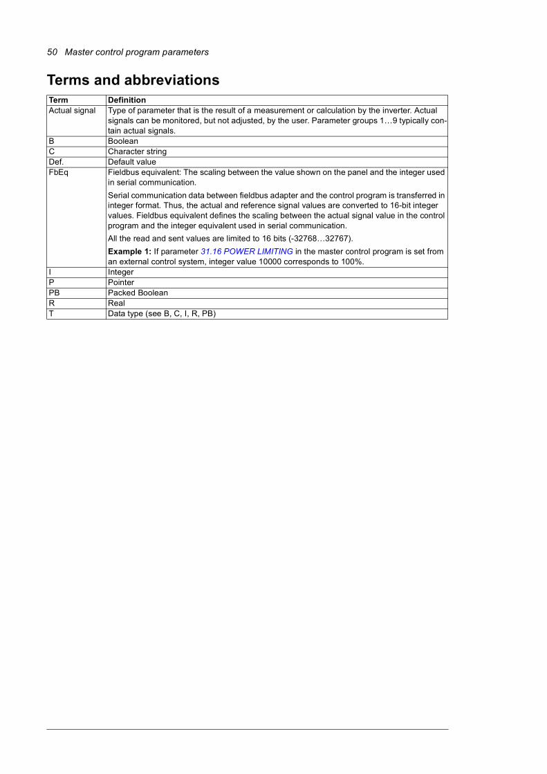
50 Master control program parameters
Terms and abbreviationsTerm DefinitionActual signal Type of parameter that is the result of a measurement or calculation by the inverter. Actual
signals can be monitored, but not adjusted, by the user. Parameter groups 1…9 typically con-tain actual signals.
B BooleanC Character stringDef. Default valueFbEq Fieldbus equivalent: The scaling between the value shown on the panel and the integer used
in serial communication.
Serial communication data between fieldbus adapter and the control program is transferred in integer format. Thus, the actual and reference signal values are converted to 16-bit integer values. Fieldbus equivalent defines the scaling between the actual signal value in the control program and the integer equivalent used in serial communication.
All the read and sent values are limited to 16 bits (-32768…32767).
Example 1: If parameter 31.16 POWER LIMITING in the master control program is set from an external control system, integer value 10000 corresponds to 100%.
I IntegerP PointerPB Packed BooleanR RealT Data type (see B, C, I, R, PB)

Master control program parameters 51
Parameter groups 01…09No. Name/Value Description T FbEq
01 ACTUAL SIGNALS Various actual signals
01.04 AC VOLTAGE L1 Measured grid voltage from the L1 phase R 1 = 1 V
01.05 AC VOLTAGE L2 Measured grid voltage from the L2 phase R 1 = 1 V
01.06 AC VOLTAGE L3 Measured grid voltage from the L3 phase R 1 = 1 V
01.07 AC CURRENT L1 Measured output current from the L1 phase R 1 = 1 A
01.08 AC CURRENT L2 Measured output current from the L2 phase R 1 = 1 A
01.09 AC CURRENT L3 Measured output current from the L3 phase R 1 = 1 A
01.10 AC POWER Measured active power of the inverter:
Positive = power flow from inverter to gridNegative = power flow from grid to inverterNote: Power values cannot be used to calculate theefficiency of inverter.
R 10 = 1 kW
01.11 AC POWER Measured active power in percent of nominal power R 100 = 1%
01.12 AC FREQUENCY Measured grid frequency R 100 = 1 Hz
01.13 COS PHI Measured cosine phi R 100 = 1
01.14 REACTIVE POWER Measured reactive power of the inverter (positive = capacitive, negative = inductive)
R 10 = 1 kVAr
01.15 GRID IMPEDANCE Reserved 1 = 1 ohm
01.16 INSUL RESISTANCE Measured insulation resistance. This signal is valid only with option +Q954.
I 1 = 1 kohm
01.17 DC VOLTAGE Reserved 1 = 1 V
01.18 DC CURRENT Measured DC current R 1 = 1 A
01.19 DC POWER Shows measured or estimated DC power. Selection between measured and estimated values can be done with parameter 14.14 DC POWER SELECT.
R 1 = 1 kW
01.20 INV TEMPERATURE Estimated IGBT temperature of the inverter unit R 1 = 1 °C
01.21 INV STATUS Shows same status as in parameter 08.04 PVA STATES (page 58).
I 1 = 1
01.22 INV FAILURE Inverter fault word PB 1 = 1
01.23 ALARM ACTIVE Inverter alarm word PB 1 = 1
01.24 MAIN STATUS WORD Shows same status as in parameter 08.01 MAIN STA-TUS WORD (page 57).
PB 1 = 1
01.25 TIME OF USAGE Elapsed time counter. Runs when the control unit of the inverter unit is powered.
I 1 = 1 h
01.26 ENERGY PRODUCED Counts the kilowatt hours of power flow from inverter to grid. Counter can be reset by parameter 16.09 RESET COUNTER in the inverter control program (see page 134).
I 1 = 100 kWh
Bit Value Description0 1 Inverter unit fault active
0 No inverter unit fault active1…15 Reserved
Bit Value Description0 1 Inverter unit alarm active
0 No inverter unit alarm active1…15 Reserved
52 Master control program parameters
01.27 kWh COUNTER Shows the kilowatts count from 01.26 ENERGY PRO-DUCED. After 999 kilowatts, this counter wraps around to 0 and 01.28 MWh COUNTER is incremented.
I 1 = 1
01.28 MWh COUNTER Shows the megawatts count from 01.26 ENERGY PRODUCED. After 999 megawatts, this counter wraps around to 0 and 01.29 GWh COUNTER is incre-mented.
I 1 = 1
01.29 GWh COUNTER Shows the gigawatts count from 01.26 ENERGY PRO-DUCED.
I 1 = 1
01.30 BREAKER COUNTER Counts main contactor closures. Counter can be reset by parameter 16.09 RESET COUNTER in the inverter control program (see page 134).
I 1 = 1
01.31 DC BREAKER COUNTR Shows the number of DC contactor closures. Counter can be reset by parameter 16.17 RESET DC BRK CNT in the inverter control program (see page 134).
I 1 = 1
01.32 ENERGY LIMITING Energy limit word PB 1 = 1
01.33 ENERGY LIM COUNTR Reserved 1 = 1
01.34 PV MODULE DC MEAS Measured solar generator voltage. I 1 = 1
01.35 SOLAR RADIATION Shows the value of the signal selected by parameter 14.01 SOLAR RADIATION (see page 66).
R 1 = 1 W/m2
01.36 SOLAR IRRADIANCE Shows the value of the signal selected by parameter 14.04 SOLAR IRRADIATION (see page 67).
R 1 = 1 W/m2
01.37 PV MODULE TEMP Shows the value of the signal selected by parameter 14.07 PV MODULE TEMP (see page 67).
R 1 = 1 °C
01.38 AMBIENT TEMP Shows the value of the signal selected by parameter 14.08 AMBIENT TEMP (see page 67).
R 1 = 1 °C
01.39 EXTERNAL TEMP Shows the value of the signal selected by parameter 14.09 EXTERNAL TEMP (see page 68).
R 1 = 1 °C
01.40 TRANSFORMER TEMP Shows the value of the signal selected by parameter 14.10 TRA OIL TEMP (see page 68).
R 1 = 1 °C
01.41 TRANSF OIL LEV Shows the value of the signal selected by parameter 14.11 TRA OIL LEVEL (see page 68).
R 1 = 1%
01.42 ISU ACTUAL 1 Data set 25, data word 1 transmitted by the inverter unit. See inverter parameter group 93 D SET TR ADDR (page 171).
I 1 = 1
01.43 ISU ACTUAL 2 Data set 25, data word 2 transmitted by the inverter unit. See inverter parameter group 93 D SET TR ADDR (page 171).
I 1 = 1
01.44 ISU ACTUAL 3 Data set 25, data word 3 transmitted by the inverter unit. See inverter parameter group 93 D SET TR ADDR (page 171).
I 1 = 1
02 ACTUAL SIGNALS Various actual signals
02.01 USED DC START LIM Actual DC voltage start limit used (after photovoltaic cell temperature correction)
I 1 = 1
02.02 GND CURRENT ACT Displays the actual grounding current measured by a PGND board (option +F282 / +F283). If the grounding option is not installed, the value of this signal is irrele-vant.
R 1 = 0.02 mA
No. Name/Value Description T FbEq
Bit Value Description0 1 Power limitation active1…15 Reserved

Master control program parameters 53
02.03 MAINS VOLTAGE Displays a mains voltage signal from the inverter con-trol program.
R 1 = 1 V
02.04 CABINET TEMP Shows the maximum value of measured cabinet temperature. This temperature is the highest tempera-ture of the two PT100 sensors in PVS800.
R 1 = 1 °C
03 ACTUAL SIGNALS Various actual signals
03.01 DC CUR INPUT 1 Shows the measured current value of DC input 1. R 10 = 1 A
03.02 DC CUR INPUT 2 Shows the measured current value of DC input 2. R 10 = 1 A
03.03 DC CUR INPUT 3 Shows the measured current value of DC input 3. R 10 = 1 A
03.04 DC CUR INPUT 4 Shows the measured current value of DC input 4. R 10 = 1 A
03.05 DC CUR INPUT 5 Shows the measured current value of DC input 5. R 10 = 1 A
03.06 DC CUR INPUT 6 Shows the measured current value of DC input 6. R 10 = 1 A
03.07 DC CUR INPUT 7 Shows the measured current value of DC input 7. R 10 = 1 A
03.08 DC CUR INPUT 8 Shows the measured current value of DC input 8. R 10 = 1 A
03.09 DC CUR INPUT 9 Shows the measured current value of DC input 9. R 10 = 1 A
03.10 DC CUR INPUT 10 Shows the measured current value of DC input 10. R 10 = 1 A
03.11 DC CUR INPUT 11 Shows the measured current value of DC input 11. R 10 = 1 A
03.12 DC CUR INPUT 12 Shows the measured current value of DC input 12. R 10 = 1 A
03.13 DC CUR INPUT 13 Shows the measured current value of DC input 13. R 10 = 1 A
03.14 DC CUR INPUT 14 Shows the measured current value of DC input 14. R 10 = 1 A
03.15 DC CUR INPUT 15 Shows the measured current value of DC input 15. R 10 = 1 A
03.16 DC CUR INPUT 16 Shows the measured current value of DC input 16. R 10 = 1 A
04 INFORMATION Program versions, control unit information
04.01 SW PACKAGE VER Displays the type and version of the firmware package. For PVS800 master control program revision 7xxx, the designation is GSXR7xxx.
C -
04.02 DTC VERSION Firmware version of a fixed part of the master control program that consists of operating system, communi-cation control of the DDCS channels, and Modbus soft-ware of the control panel
C -
04.03 APPLIC NAME Displays the type and the version of the control pro-gram.
C -
04.04 BOARD TYPE Control board type C -
04.05 INV NOM POWER Nominal power of the inverter unit R 1 = 1
05 ANALOGUE INPUTS Values of analog inputs
05.01 BASIC AI1 Value of control unit analog input AI1 ±20000 = ±10 volts.
I 1 = 1
-20000…20000 Value
05.02 BASIC AI2 Value of control unit analog input AI2 ±20000 = ±20 mA.
I 1 = 1
-20000…20000 Value
05.03 BASIC AI3 Value of control unit analog input AI3 ±20000 = ±20 mA.
I 1 = 1
-20000…20000 Value
05.04 EXT1 AI1 Value of extension module 1 analog input AI1 I 1 = 1
-20000…20000 Value
05.05 EXT1 AI2 Value of extension module 1 analog input AI2 I 1 = 1
-20000…20000 Value
No. Name/Value Description T FbEq

54 Master control program parameters
05.06 EXT2 AI1 Value of extension module 2 analog input AI1 I 1 = 1
-20000…20000 Value
05.07 EXT2 AI2 Value of extension module 2 analog input AI2 I 1 = 1
-20000…20000 Value
05.08 EXT3 AI1 Value of extension module 3 analog input AI1 I 1 = 1
-20000…20000 Value
05.09 EXT3 AI2 Value of extension module 3 analog input AI2 I 1 = 1
-20000…20000 Value
05.10 EXT4 AI1 Value of extension module 4 analog input AI1 I 1 = 1
-20000…20000 Value
05.11 EXT4 AI2 Value of extension module 4 analog input AI2 I 1 = 1
-20000…20000 Value
05.12 EXT5 AI1 Value of extension module 5 analog input AI1 I 1 = 1
-20000…20000 Value
05.13 EXT5 AI2 Value of extension module 5 analog input AI2 I 1 = 1
-20000…20000 Value
05.14 EXT6 AI1 Value of extension module 6 analog input AI1 I 1 = 1
-20000…20000 Value
05.15 EXT6 AI2 Value of extension module 6 analog input AI2 I 1 = 1
-20000…20000 Value
05.16 EXT7 AI1 Value of extension module 7 analog input AI1 I 1 = 1
-20000…20000 Value
05.17 EXT7 AI2 Value of extension module 7 analog input AI2 I 1 = 1
-20000…20000 Value
05.18 EXT8 AI1 Value of extension module 8 analog input AI1 I 1 = 1
-20000…20000 Value
05.19 EXT8 AI2 Value of extension module 8 analog input AI2 I 1 = 1
-20000…20000 Value
05.20 EXT9 AI1 Value of extension module 9 analog input AI1 I 1 = 1
-20000…20000 Value
05.21 EXT9 AI2 Value of extension module 9 analog input AI2 I 1 = 1
-20000…20000 Value
06 ANALOGUE OUTPUTS
Values of analog outputs
06.01 BASIC AO1 Value of control unit analog output AO1 R 1 = 1483
0…20 mA Value
06.02 BASIC AO2 Value of control unit analog output AO2 R 1 = 1483
0…20 mA Value
06.03 EXT1 AO1 Value of extension module 1 analog output AO1 R 1 = 1483
0…20 mA Value
06.04 EXT1 AO2 Value of extension module 1 analog output AO2 R 1 = 1483
0…20 mA Value
06.05 EXT2 AO1 Value of extension module 2 analog output AO1 R 1 = 1483
0…20 mA Value
No. Name/Value Description T FbEq

Master control program parameters 55
06.06 EXT2 AO2 Value of extension module 2 analog output AO2 R 1 = 1483
0…20 mA Value
06.07 EXT3 AO1 Value of extension module 3 analog output AO1 R 1 = 1483
0…20 mA Value
06.08 EXT3 AO2 Value of extension module 3 analog output AO2 R 1 = 1483
0…20 mA Value
06.09 EXT4 AO1 Value of extension module 4 analog output AO1 R 1 = 1483
0…20 mA Value
06.10 EXT4 AO2 Value of extension module 4 analog output AO2 R 1 = 1483
0…20 mA Value
06.11 EXT5 AO1 Value of extension module 5 analog output AO1 R 1 = 1483
0…20 mA Value
06.12 EXT5 AO2 Value of extension module 5 analog output AO2 R 1 = 1483
0…20 mA Value
06.13 EXT6 AO1 Value of extension module 6 analog output AO1 R 1 = 1483
0…20 mA Value
06.14 EXT6 AO2 Value of extension module 6 analog output AO2 R 1 = 1483
0…20 mA Value
06.15 EXT7 AO1 Value of extension module 7 analog output AO1 R 1 = 1483
0…20 mA Value
06.16 EXT7 AO2 Value of extension module 7 analog output AO2 R 1 = 1483
0…20 mA Value
06.17 EXT8 AO1 Value of extension module 8 analog output AO1 R 1 = 1483
0…20 mA Value
06.18 EXT8 AO2 Value of extension module 8 analog output AO2 R 1 = 1483
0…20 mA Value
06.19 EXT9 AO1 Value of extension module 9 analog output AO1 R 1 = 1483
0…20 mA Value
06.20 EXT9 AO2 Value of extension module 9 analog output AO2 R 1 = 1483
0…20 mA Value
07 CONTROL WORDS Control words.
Main Control Word (MCW) is the principal means of controlling the PVS800 from an overriding system.
Bits of the Main Control Word can be overridden locally using the control panel or a PC, the standard I/O, or an adaptive program. Master control program of the PVS800 switches between its states according to the bit-coded instructions of the final control word.
07.01 MAIN CTRL WORD Main Control Word (MCW), received from the overrid-ing control system (see also parameter 90.01 D SET 10 VAL 1).
PB
No. Name/Value Description T FbEq

56 Master control program parameters
07.02 USED MCW Shows the final control word that is used as the input for the PVS800 state machine (see page 31). For bit definitions, see parameter 07.01 MAIN CTRL WORD.
PB
07.03 MAIN CTRL W MASK Mask word for control word 07.01 MAIN CTRL WORD. If the mask is not used, set to FFFF (65535 int.). If, for example, bit 0 is masked, set to FFFE (65534 int.). Several bits can be masked at the same time.
Mask function is needed if there is a need to share the control of bits between the overriding system and the adaptive program (or I/O control). See parameter 66.01 CW, and the block CW in the Application guide: Adap-tive program for PVS800 central inverters (3AUA0000091276 [English]).
PB
07.04 ISU MCW Shows the Main Control Word in use for the inverter unit (modified from 07.02 USED MCW). This word is the output of the PVS800 state machine (see page 31). For bit definitions, see 07.01 MAIN CTRL WORD.
PB
07.05 GND CTRL WORD Displays an internal control word of the DC grounding. PB
No. Name/Value Description T FbEq
Bit Name Value Description0 ON/OFF 0 1 Inverter operation is enabled. Bit 0 and bit 3 must be
controlled at the same time.0 Operation is disabled.
1, 2 Reserved3 ON/OFF 0 1 Operation is enabled. Bit 0 and bit 3 must be
controlled at the same time.0 Operation is disabled.
4…6 Reserved7 RESET 0 1 Reset8…15 Reserved
Local CWControl panel or PC
Local control on/off
07.01
07.02BITOR
BITAND
BITOR
Overriding sys-tem
I/O
Adaptive program (66.01)
Mask (07.03)
Bit Value Description0 0 Mask
1 No mask1...15 0 Mask
1 No mask

Master control program parameters 57
08 STATUS WORDS Status words. See also the control block diagrams in chapter Program features. Status Word (SW) is a word containing status information, sent by the PVS800 master control program to the external control system.
08.01 MAIN STATUS WORD Main Status Word. Combined from the Status Word of the inverter unit, and communication faults. Sent to the overriding control system. See 92 D SET TR ADDR.
PB
08.02 DI STATUS WORD Digital input status word. PB
No. Name/Value Description T FbEq
Bit Name Value Description0 MPPT_MODE 1 Inverter is in the MPPT mode.1 INSULATION_OK 1 Insulation is OK.2 DC_TO_GROUND_VOLTAGE 1 DC to the GND voltage is present.3 START_REQUEST 1 Start is requested.
Bit Name Value STATE/Description0 RDY_ON 1 Ready to switch on = no fault
0 Not ready to switch on = fault1 RDY_RUN 1 Ready to operate = DC bus charged
0 Not ready to operate2 RDY_REF 1 Operation enabled
0 Operation inhibited3 TRIPPED 1 A fault occurred in the inverter.4 HVRT 1 HVRT is ongoing.
0 No HVRT5...6 Reserved7 ALARM 1 A warning in the inverter.8 MODULATING 1 Inverter is modulating.
0 Inverter is not modulating.9 REMOTE 1 Control location: REMOTE
0 Control location: LOCAL10 NET OK 1 Grid voltage is OK.
0 Grid voltage is lost.11 VOLTAGE DIP 1 Voltage dip is ongoing.
0 No voltage dip12 Reserved13 CHARGING
OR RDY_RUN
Combines bits 14 and 1.1 Ready to operate = DC bus charged or
charging contactor closed.0 Not ready to operate or charging contactor
open.14 CHARGING 1 Charging contactor closed
0 Charging contactor open15 Reserved
Bit Name Description0 Reserved1 DI1 Status of digital input 1 of control unit2 DI2 Status of digital input 2 of control unit3 DI3 Status of digital input 3 of control unit4 DI4 Status of digital input 4 of control unit5 DI5 Status of digital input 5 of control unit6 DI6 Status of digital input 6 of control unit7 DI7 (DIIL) Status of digital input 7 of control unit8…15 Reserved

58 Master control program parameters
08.03 EXT DI STATUS W Extension module digital input status word. See also parameters 98.04…98.08.
PB
08.04 PVA STATES Indicates the state of the master control program. See section PVS800 state machine on page 31.
I -
STANDBY Power on, no faults, inverter unit not in the local mode 1
SLEEP Start on but all start conditions have not been met. 2
START ISU Start on, all start conditions are met. Start command sent to the inverter unit.
3
MPPT Maximum power point tracking (MPPT) mode active. See section Maximum power point tracking (MPPT) on page 34.
4
ISU LOCAL Inverter unit is switched into the local control mode. 5
FAULTED Fault has occurred. 6
Q POWER Inverter is in the reactive power compensation mode. See section Reactive power compensation on page 37.
7
No. Name/Value Description T FbEq
Bit Name Description0 Reserved1 EXT1_DI1 Digital input 1 status on RDIO extension module 12 EXT1_DI2 Digital input 2 status on RDIO extension module 13 EXT1_DI3 Digital input 3 status on RDIO extension module 14 EXT2_DI1 Digital input 1 status on RDIO extension module 25 EXT2_DI2 Digital input 2 status on RDIO extension module 26 EXT2_DI3 Digital input 3 status on RDIO extension module 27 EXT3_DI1 Digital input 1 status on RDIO extension module 38 EXT3_DI2 Digital input 2 status on RDIO extension module 39 EXT3_DI3 Digital input 3 status on RDIO extension module 310 EXT4_DI1 Digital input 1 status on RDIO extension module 411 EXT4_DI2 Digital input 2 status on RDIO extension module 412 EXT4_DI3 Digital input 3 status on RDIO extension module 413 EXT5_DI1 Digital input 1 status on RDIO extension module 514 EXT5_DI2 Digital input 2 status on RDIO extension module 515 EXT5_DI3 Digital input 3 status on RDIO extension module 5
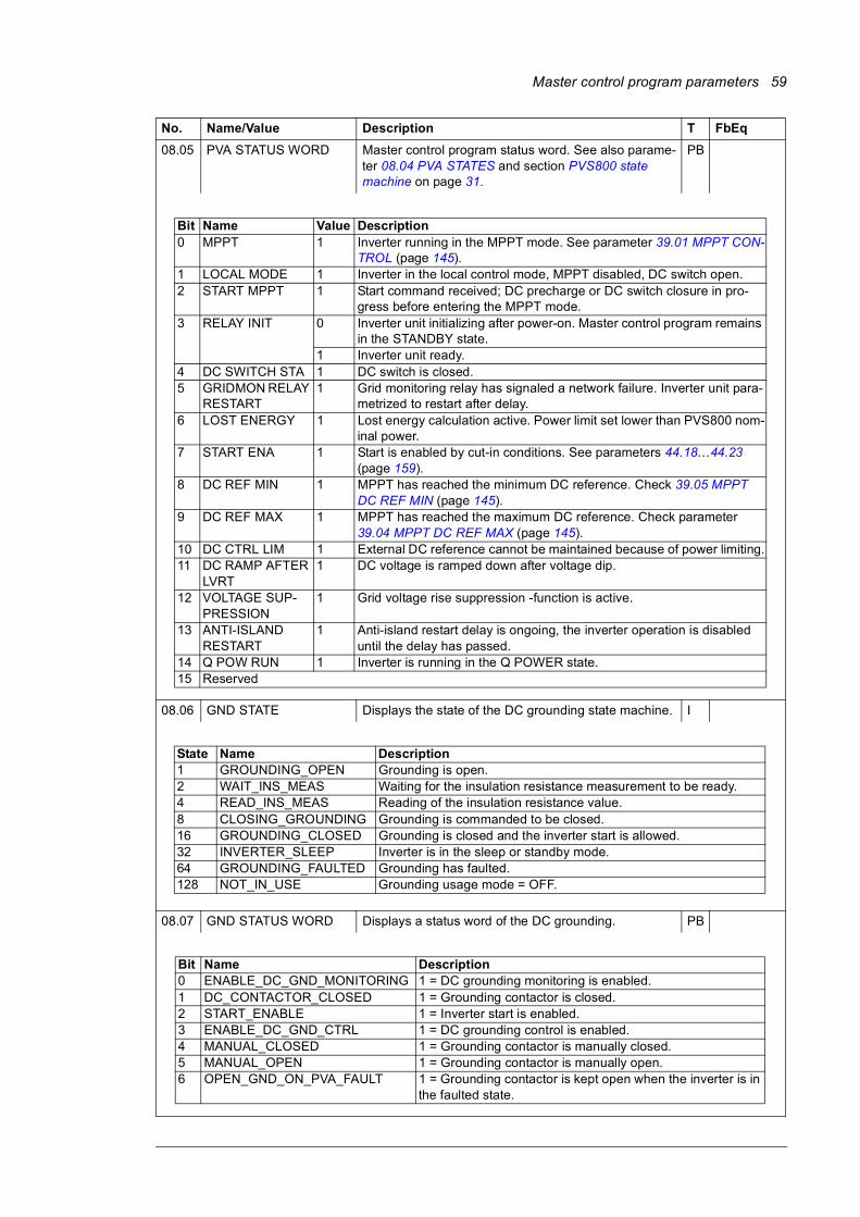
Master control program parameters 59
08.05 PVA STATUS WORD Master control program status word. See also parame-ter 08.04 PVA STATES and section PVS800 state machine on page 31.
PB
08.06 GND STATE Displays the state of the DC grounding state machine. I
08.07 GND STATUS WORD Displays a status word of the DC grounding. PB
No. Name/Value Description T FbEq
Bit Name Value Description0 MPPT 1 Inverter running in the MPPT mode. See parameter 39.01 MPPT CON-
TROL (page 145).1 LOCAL MODE 1 Inverter in the local control mode, MPPT disabled, DC switch open.2 START MPPT 1 Start command received; DC precharge or DC switch closure in pro-
gress before entering the MPPT mode.3 RELAY INIT 0 Inverter unit initializing after power-on. Master control program remains
in the STANDBY state.1 Inverter unit ready.
4 DC SWITCH STA 1 DC switch is closed.5 GRIDMON RELAY
RESTART1 Grid monitoring relay has signaled a network failure. Inverter unit para-
metrized to restart after delay.6 LOST ENERGY 1 Lost energy calculation active. Power limit set lower than PVS800 nom-
inal power.7 START ENA 1 Start is enabled by cut-in conditions. See parameters 44.18…44.23
(page 159).8 DC REF MIN 1 MPPT has reached the minimum DC reference. Check 39.05 MPPT
DC REF MIN (page 145).9 DC REF MAX 1 MPPT has reached the maximum DC reference. Check parameter
39.04 MPPT DC REF MAX (page 145).10 DC CTRL LIM 1 External DC reference cannot be maintained because of power limiting.11 DC RAMP AFTER
LVRT1 DC voltage is ramped down after voltage dip.
12 VOLTAGE SUP-PRESSION
1 Grid voltage rise suppression -function is active.
13 ANTI-ISLAND RESTART
1 Anti-island restart delay is ongoing, the inverter operation is disabled until the delay has passed.
14 Q POW RUN 1 Inverter is running in the Q POWER state.15 Reserved
State Name Description1 GROUNDING_OPEN Grounding is open.2 WAIT_INS_MEAS Waiting for the insulation resistance measurement to be ready.4 READ_INS_MEAS Reading of the insulation resistance value.8 CLOSING_GROUNDING Grounding is commanded to be closed.16 GROUNDING_CLOSED Grounding is closed and the inverter start is allowed.32 INVERTER_SLEEP Inverter is in the sleep or standby mode.64 GROUNDING_FAULTED Grounding has faulted.128 NOT_IN_USE Grounding usage mode = OFF.
Bit Name Description0 ENABLE_DC_GND_MONITORING 1 = DC grounding monitoring is enabled.1 DC_CONTACTOR_CLOSED 1 = Grounding contactor is closed.2 START_ENABLE 1 = Inverter start is enabled.3 ENABLE_DC_GND_CTRL 1 = DC grounding control is enabled.4 MANUAL_CLOSED 1 = Grounding contactor is manually closed.5 MANUAL_OPEN 1 = Grounding contactor is manually open.6 OPEN_GND_ON_PVA_FAULT 1 = Grounding contactor is kept open when the inverter is in
the faulted state.

60 Master control program parameters
08.08 LIMIT WORD Limit word from the Inverter control program signal 08.03 LIMIT WORD.
PB 1 = 1
09 FAULT WORDS Fault words. For possible causes and remedies, see chapter Fault tracing.
09.10 IO FAULT WORD Digital and analog extension module and control unit digital and analog I/O fault word.
PB
09.11 SUPPLY FAULT WORD Fault word from the inverter control unit. PB
No. Name/Value Description T FbEq
Bit Name Description0 DIO EXT1 ERROR Error detected in digital extension module 1.1 DIO EXT2 ERROR Error detected in digital extension module 2.2 DIO EXT3 ERROR Error detected in digital extension module 3.3 DIO EXT4 ERROR Error detected in digital extension module 4.4 DIO EXT5 ERROR Error detected in digital extension module 5.5 RMIO DIO ERROR DIGITAL IO (5442) (page 180)6 EXT RDIO ERROR EXT DIO (7082) (page 181)7 Reserved8 AIO EXT1 ERROR Error detected in analog extension module 1.9 AIO EXT2 ERROR Error detected in analog extension module 2.10 AIO EXT3 ERROR Error detected in analog extension module 3.11 AIO EXT4 ERROR Error detected in analog extension module 4.12 AIO EXT5 ERROR Error detected in analog extension module 5.13 RMIO AIO ERROR ANALOG IO (5441) (page 179)14 EXT RAIO ERROR EXT AIO (7081) (page 181)15 Reserved
Bit Fault0 >CHARGING F (3284) (page 179)1 >OVERCURR (2380) (page 183)2 >EXT DI5 (1081) (page 181)3 >PVS800 TEMP (4291) (page 183)4 >EXT DI4 (1080) (page 181)5 >EXT DI1 (1082) (page 181)6 >MAIN CNT F (2384) (page 182)7 >SHORT CIRC (2381) (page 184)8 >INTERNAL F (1083) (page 182)9 >NET VOLT (3285) (page 183)10 >COMM MODULE (7581) (page 180)11 >EXT DI7 (FF96) (page 181)12 >EARTH FAULT (2383) (page 180)13 >SYNCHRO FLT (8180) (page 184)14 >DC UNDERVLT (3282) (page 180)15 DC OVERVOLT (32AF) (page 180)Bit value: 1 = fault, 0 = no fault

Master control program parameters 61
09.12 SUPPLY ALARM WORD Alarm word from the inverter control unit. PB
09.13 AP FW Alarm and fault word for the user’s events. Defined by function block A/F WORD. See Application guide: Adaptive program for PVS800 central inverters (3AUA0000091276 [English]).
PB
09.14 PVA FAULT WORD Fault word PB
No. Name/Value Description T FbEq
Bit Fault0 >COMM MODULE (758A) (page 180)1 >PANEL LOST (5382) (page 183)2 >EXT DI1 ALM (1089) (page 181)3 Reserved4 >PVS800 TEMP (4292) (page 183)5 Reserved6 >PLIM EXT TMP (44AB) (page 183)7 >QLIM EXT TMP (44AC) (page 184)8 >QLIM PVS TMP (818F) (page 184)9 >RUN DISABLE (8194) (page 184)10 >NET LOST (32A6) (page 183)11 >EXT DI7 ALM (108C) (page 181)12 >RECHARGE ALM (32AA) (page 184)13 >EXT DI4 ALM (108A) (page 181)14 >EXT DI5 ALM (108B) (page 181)15 ReservedBit value: 1 = fault, 0 = no fault
Bit Fault0 COMM MODULE (7510) (page 180)1 CH2 COM LOSS (7520) (page 180)2 >REVERSE POW (8187) (page 184)3 >DC BRK TRP (8188) (page 180)4 >GRID MONFLT (8189) (page 182)5 >DC BRK LEV (818C) (page 180)6 >DC BRK POS (818D) (page 180)7 >BACKPOW LEV (818E) (page 179)8 AUTORESET F (6080) (page 179)9 EXT EVNT DI3 (9083) (page 181)10 EXT EVNT DI4 (9084) (page 181)11 EXT EVNT DI5 (9085) (page 181)12 >ANTI-ISLAND (819F) (page 179)13 EM STOP (F083) (page 180)14 ISU FAULT (8185) (page 182)15 ReservedBit value: 1 = fault, 0 = no fault

62 Master control program parameters
09.15 PVA ALARM WORD Alarm word PB
09.16 INV LAST FLT CODE Shows the latest fault code of the inverter control unit. PB 1 = 1
09.17 PVA ALARM WORD 2 Alarm word PB 1 = 1
09.18 IO FAULT WORD 2 Fault word PB 1 = 1
09.20 FAULT CODE 1 LAST Fieldbus code of the latest fault. See chapter Fault tracing.
PB 1 = 1
09.21 FAULT CODE 2 LAST Fieldbus code of the 2nd latest fault. See chapter Fault tracing.
PB 1 = 1
09.22 FAULT CODE 3 LAST Fieldbus code of the 3rd latest fault. See chapter Fault tracing.
PB 1 = 1
09.23 FAULT CODE 4 LAST Fieldbus code of the 4th latest fault. See chapter Fault tracing.
PB 1 = 1
09.24 FAULT CODE 5 LAST Fieldbus code of the 5th latest fault. See chapter Fault tracing.
PB 1 = 1
09.25 WARN CODE 1 LAST Fieldbus code of the latest alarm. See chapter Fault tracing.
PB 1 = 1
09.26 WARN CODE 2 LAST Fieldbus code of the 2nd latest alarm. See chapter Fault tracing.
PB 1 = 1
09.27 WARN CODE 3 LAST Fieldbus code of the 3rd latest alarm. See chapter Fault tracing.
PB 1 = 1
No. Name/Value Description T FbEq
Bit Alarm0 Reserved1 >PVS&PANEL DC (32A9) (page 183)2 PVA RUN ENA (FF54) (page 183). See also parameter 08.05 PVA
STATUS WORD bit 3.3 AUTORESET A (6081) (page 179)4 DC INPUT DEV (2185) (page 180)5 >LOST ENERGY (8190) (page 182)6 UDC HIGH LIM (32A7) (page 184)7 EXT EVNT DI3 (9083) (page 181)8 EXT EVNT DI4 (9084) (page 181)9 EXT EVNT DI5 (9085) (page 181)10 Reserved11 RMBA LOST (61A9) (page 184)12 APP OVERLOAD (FFD9) (page 179)13 APPLIC 1 FLT (FFD6) (page 179)14 APPLIC 2 FLT (FFD7) (page 179)15 IO START ENA (61AA) (page 182)Bit value: 1 = alarm, 0 = no alarm
Bit Alarm0 >MPPT MIN REF (32AD) (page 183)1 >MPPT MAX REF (32AE) (page 183)2 ISU WARNING (8186) (page 182)
Bit Name Description0 AIO EXT6 ERROR Error detected in analog extension module 6.1 AIO EXT7 ERROR Error detected in analog extension module 7.2 AIO EXT8 ERROR Error detected in analog extension module 8.3 AIO EXT9 ERROR Error detected in analog extension module 9.

Master control program parameters 63
09.28 WARN CODE 4 LAST Fieldbus code of the 4th latest alarm. See chapter Fault tracing.
PB 1 = 1
09.29 WARN CODE 5 LAST Fieldbus code of the 5th latest alarm. See chapter Fault tracing.
PB 1 = 1
No. Name/Value Description T FbEq

64 Master control program parameters
Parameter groups 10…99No. Name/Value Description Def T FbEq
10 CMD GROUP Special commands
10.01 RESET CMD By setting this parameter to RESET, the reset command is sent to a faulted inverter unit.
Value returns to NOT SET automatically after RESET.
NOT SET B
NOT SET 0
RESET 65535
10.02 ENABLE I/O CTRL Enables/disables the I/O control, ie, PVS800 control through digital inputs.
When the I/O control is enabled, start/stop and reset signals are read from inputs that are defined by parameters 10.04 I/O START SOURCE and 10.05 I/O RESET SOURCE.
I/O control is parallel to the fieldbus and adaptive control words (see parameter 07.02 USED MCW). Local control over-rides I/O control.
NO B
NO I/O control disabled 0
YES I/O control enabled 1
10.03 EM STOP AUTORESET
Enables/disables an automatic reset of the emergency stop relay. See the Hardware manual.
If enabled, digital output DO1 cannot be used for other purposes.
NO I
NO Automatic reset disabled 1
DO1 Automatic reset of emergency stop relay enabled through digital output DO1. Reset pulse is active for 4 seconds after the aux-iliary power is switched on.
2
10.04 I/O START SOURCE Defines the source of the start/stop signal in I/O control (see parameter 10.02 ENABLE I/O CTRL).
WARNING! If the I/O control is enabled and a start command is
active, the PVS800 will start after the auxil-iary power to the control units has switched on.
Default source is digital input DI2 on the master control unit.
+.008.002.02 P
-255.255.31 … +255.255.31 /
C. -32768 …C. 32767
Parameter pointer: Inversion, group, index and bit fields. Bit number is effective only for blocks handling Boolean inputs.
10.05 I/O RESET SOURCE Defines the source of the reset signal in the I/O control (see parameter 10.02 ENABLE I/O CTRL).
Default source is digital input DI1 on the master control unit.
+.008.002.01 P
-255.255.31 … +255.255.31 /
C. -32768 …C. 32767
Parameter pointer: Inversion, group, index and bit fields. Bit number is effective only for blocks handling Boolean inputs.

Master control program parameters 65
13 ANALOGUE INPUTS Configuration of analog inputs.
The settings of I/O extension module 5 also apply to I/O extension modules 6, 7, 8 and 9.
13.02 AI1 FILTER ms Defines the filter time constant in millisec-onds for analog input AI1.
Note: Analog input AI1 is reserved for DC current measurement. Do not change the value of this parameter.
1000 I
1…30000 Value 1 = 1 ms
13.03 AI2 CONV MODE Defines the conversion mode for analog input AI2.
NORMAL I
NORMAL Normal scaling: -20 mA … 0 … 20 mA = -20000…0…20000
1
4 mA 4 mA scaling: 4 mA … 20 mA = 0…20000 I 2
13.04 AI2 FILTER ms Defines the filter time constant in millisec-onds for analog input AI2.
1
1…30000 Value 1 = 1 ms
13.06 AI3 FILTER ms Defines the filter time constant in millisec-onds for analog input AI3.
100 I
1…30000 Value 1 = 1 ms
13.15 EXT1 AI1 HW MODE Configures the inputs and outputs of an RAIO analog I/O extension module. Oper-ating mode of the analog inputs can be selected by using the configuration DIP switch (S2) on the circuit board of the mod-ule. Parameters must be set accordingly.
UNIPOLAR I
UNIPOLAR Unipolar input mode 1
BIPOLAR Bipolar input mode 2
No. Name/Value Description Def T FbEq
ON
1 2 3 4 5 6
ON
1 2 3 4 5 6
ON
1 2 3 4 5 6
ON
1 2 3 4 5 6
Bipolar mode (positive and negative signals)
±0(4)…20 mA±0(2)…10 V±0…2 V
Unipolar mode (positive signals only) Default
0(4)…20 mA0(2)…10 V0…2 V
RAIO-01 switch S2 settings (operating mode):
Analog input AI1 Analog input AI2
Analog input AI1 Analog input AI2

66 Master control program parameters
13.16 EXT1 AI2 HW MODE See parameter 13.15 EXT1 AI1 HW MODE.
UNIPOLAR I
UNIPOLAR Unipolar input mode 1
BIPOLAR Bipolar input mode 2
13.17 EXT1 AI1 CONV MOD Defines the conversion mode for extension module 1 analog input AI1. Scaling is the same in both conversion modes (unipolar, bipolar).
NORMAL I
NORMAL Normal scaling:
-20 mA / -2 V / -10 V … 0 … 20 mA / 2 V / 10 V = -20000 … 0 … 20000
1
4 mA 4 mA scaling: 4…20 mA = 0…20000 2
PT100 Scaling with Pt100 temperature measure-ment: 200 °C = 20000 if analog output feeds the following constant current to the Pt100 sensor:
with 1 × Pt100: = 10 mAwith 2 × Pt100: = 5 mAwith 3 × Pt100: = 3.3 mA.
3
13.18 EXT1 AI2 CONV MOD See parameter 13.17 EXT1 AI1 CONV MOD.
NORMAL I
13.19 EXT1 AI1 FILT ms Defines the filter time constant in millisec-onds for external module 1 analog input AI1.
1000 I
0…30000 Value 1 = 1 ms
13.20 EXT1 AI2 FILT ms Defines the filter time constant in millisec-onds for external module 1 analog input AI2.
1000 I
0…30000 Value 1 = 1 ms
14 ACT SIGNAL SEL Source selection for various actual signals
14.01 SOLAR RADIATION Defines a source signal that is linearly scaled by parameters 14.02 SOLAR RADIAT MIN and 14.03 SOLAR RADIAT MAX, and then shown by parameter 01.35 SOLAR RADIATION.
+.000.000.00 P
-255.255.31 … +255.255.31 /
C. -32768 … C. 32767
Parameter pointer or a constant value:
• Parameter pointer: Inversion, group, index and bit fields. Bit number is effective only for blocks handling Boolean inputs.
• Constant value: Inversion and constant fields. Inversion field must have value C to enable the constant setting.
14.02 SOLAR RADIAT MIN Defines the value displayed by 01.35 SOLAR RADIATION when the source sig-nal selected by 14.01 SOLAR RADIATION is 0.
0 I
-32768…32767 Display value corresponding to signal value of 0
1 = 1
No. Name/Value Description Def T FbEq

Master control program parameters 67
14.03 SOLAR RADIAT MAX Defines the value displayed by 01.35 SOLAR RADIATION when the source sig-nal selected by 14.01 SOLAR RADIATION is 20000.
20000 I
-32768…32767 Display value corresponding to signal value of 20000
1 = 1
14.04 SOLAR IRRADIATION Defines a source signal that is linearly scaled by parameters 14.05 SOLAR IRRAD MIN and 14.06 SOLAR IRRAD MAX, and then shown by parameter 01.36 SOLAR IRRADIANCE.
+.000.000.00 P
-255.255.31 … +255.255.31 /
C. -32768 … C. 32767
Parameter pointer or a constant value:
• Parameter pointer: Inversion, group, index and bit fields. Bit number is effective only for blocks handling Boolean inputs.
• Constant value: Inversion and constant fields. Inversion field must have value C to enable the constant setting.
14.05 SOLAR IRRAD MIN Defines the value displayed by 01.36 SOLAR IRRADIANCE when the source signal selected by 14.04 SOLAR IRRADIA-TION is 0.
0 I
-32768…32767 Display value corresponding to signal value of 0
1 = 1
14.06 SOLAR IRRAD MAX Defines the value displayed by 01.36 SOLAR IRRADIANCE when the source signal selected by 14.04 SOLAR IRRADIA-TION is 20000.
20000 I
-32768…32767 Display value corresponding to signal value of 20000
1 = 1
14.07 PV MODULE TEMP Defines a source signal that is shown by parameter 01.37 PV MODULE TEMP.
+.000.000.00 P
-255.255.31 … +255.255.31 /
C. -32768 … C. 32767
Parameter pointer or a constant value:
• Parameter pointer: Inversion, group, index and bit fields. Bit number is effective only for blocks handling Boolean inputs.
• Constant value: Inversion and constant fields. Inversion field must have value C to enable the constant setting.
14.08 AMBIENT TEMP Defines a source signal that is shown by parameter 01.38 AMBIENT TEMP.
+.000.000.00 P
-255.255.31 … +255.255.31 /
C. -32768 … C. 32767
Parameter pointer or a constant value:
• Parameter pointer: Inversion, group, index and bit fields. Bit number is effective only for blocks handling Boolean inputs.
• Constant value: Inversion and constant fields. Inversion field must have value C to enable the constant setting.
No. Name/Value Description Def T FbEq

68 Master control program parameters
14.09 EXTERNAL TEMP Defines a source signal that is shown by parameter 01.39 EXTERNAL TEMP.
+.000.000.00 P
-255.255.31 … +255.255.31 /
C. -32768 … C. 32767
Parameter pointer or a constant value:
• Parameter pointer: Inversion, group, index and bit fields. Bit number is effective only for blocks handling Boolean inputs.
• Constant value: Inversion and constant fields. Inversion field must have value C to enable the constant setting.
14.10 TRA OIL TEMP Defines a source signal that is shown by parameter 01.40 TRANSFORMER TEMP.
+.000.000.00 P
-255.255.31 … +255.255.31 /
C. -32768 … C. 32767
Parameter pointer or a constant value:
• Parameter pointer: Inversion, group, index and bit fields. Bit number is effective only for blocks handling Boolean inputs.
• Constant value: Inversion and constant fields. Inversion field must have value C to enable the constant setting.
14.11 TRA OIL LEVEL Defines a source signal that is linearly scaled by parameters 14.12 TRA OIL LEVEL MIN and 14.13 TRA OIL LEVEL MAX, and then shown by parameter 01.41 TRANSF OIL LEV.
+.000.000.00 P
-255.255.31 … +255.255.31 /
C. -32768 … C. 32767
Parameter pointer or a constant value:
• Parameter pointer: Inversion, group, index and bit fields. Bit number is effective only for blocks handling Boolean inputs.
• Constant value: Inversion and constant fields. Inversion field must have value C to enable the constant setting.
14.12 TRA OIL LEVEL MIN Defines the value displayed by 01.41 TRANSF OIL LEV when the source signal selected by 14.11 TRA OIL LEVEL is 0.
0 I
-32768…32767 Display value corresponding to signal value of 0
1 = 1
14.13 TRA OIL LEVEL MAX Defines the value displayed by 01.41 TRANSF OIL LEV when the source signal selected by 14.11 TRA OIL LEVEL is 20000.
20000 I
-32768…32767 Display value corresponding to signal value of 20000
1 = 1
14.14 DC POWER SELECT Selection between measured and esti-mated DC power.
MEASURED
MEASURED 01.19 DC POWER = 01.34 PV MODULE DC MEAS x 01.18 DC CURRENT / 1000
1
ESTIMATED 01.19 DC POWER = Estimated DC power from the inverter control program.
2
No. Name/Value Description Def T FbEq

Master control program parameters 69
15 ANALOGUE OUTPUTS
It is possible to select a signal or parame-ter to control the analog outputs. Outputs can also be controlled from an overriding system.
15.01 AO1 OFFSET Defines analog output AO1 signal offset in milliamperes.
0 mA R
0 mA … 20 mA Value 1000 = 1 mA
15.02 AO1 SCALE Defines the scale for analog output AO1. Defines the integer value that corresponds to the maximum output current (20 mA), eg, 20000 (default) = 20 mA.
20000 I
0…30000 Integer value
15.03 AO2 OFFSET See parameter 15.01 AO1 OFFSET. 0 mA R
0 mA … 20 mA Value 1000 = 1 mA
15.04 AO2 SCALE See parameter 15.02 AO1 SCALE. 20000 I
0…30000 Integer value
15.05 EXT1 AO1 OFFSET See parameter 15.01 AO1 OFFSET. 0 mA R
0 mA … 20 mA Value 1000 = 1 mA
15.06 EXT1 AO1 SCALE See parameter 15.02 AO1 SCALE. 20000 I
0…30000 Integer value
15.07 EXT1 AO2 OFFSET See parameter 15.01 AO1 OFFSET. 0 mA R
0 mA … 20 mA Value 1000 = 1 mA
15.08 EXT1 AO2 SCALE See parameter 15.02 AO1 SCALE. 20000 I
0…30000 Integer value
… … … … … …
15.37 EXT9 AO1 OFFSET See parameter 15.01 AO1 OFFSET. 0 mA R
0 mA … 20 mA Value 1000 = 1 mA
15.38 EXT9 AO1 SCALE See parameter 15.02 AO1 SCALE. 20000 I
0…30000 Integer value
15.39 EXT9 AO2 OFFSET See parameter 15.01 AO1 OFFSET. 0 mA R
0 mA … 20 mA Value 1000 = 1 mA
15.40 EXT9 AO2 SCALE See parameter 15.02 AO1 SCALE. 20000 I
0…30000 Integer value
16 SYSTEM CTR INPUT Parameter lock, local lock, parameter backup
16.01 LOCAL CTRL LOST Defines the action taken when the commu-nication with the local control device (con-trol panel or PC tool) is lost.
NO ACTION I
NO ACTION Loss of local control device does not cause an alarm or fault, or stop the master control program.
WARNING! The PVS800 cannot be stopped if the master control program
is set to the local control mode and the control device is not available.
1
No. Name/Value Description Def T FbEq

70 Master control program parameters
STOP PVA Loss of local control device causes an alarm and stops the master control pro-gram.
2
16.02 PARAMETER LOCK Selects the state of the parameter lock. With the parameter lock, you can prevent unauthorized changes by CDP 312R or the DriveWindow tool for parameter groups 0…99.
OPEN B
LOCKED Parameter changes are disabled. 65535
OPEN Parameter changes are enabled. 0
16.03 PASS CODE Selects the pass code for the parameter lock. Default value of this parameter is 0. To open the parameter lock, change the value to 358. After the parameter lock is opened, the value changes automatically back to 0.
0 I
0…30000 1 = 1
16.04 LOCAL LOCK Disables entering the local control mode (LOC/REM key on the panel).
WARNING! Before activating, ensure that the control panel is not needed
for stopping the PVS800!
FALSE B
FALSE Local control allowed 0
TRUE Local control disabled 65535
16.05 PARAMETER BACKUP
Saves parameters from the RAM memory to the FPROM memory. Saving of parame-ters is needed only when parameter changes through an external control sys-tem have to be stored to the FPROM memory.
Note: Parameter changes via the control panel or DriveWindow are immediately saved to the FPROM memory.
DONE I
DONE Parameter saving is completed. 0
SAVE Parameters are saved to the FPROM memory.
1
19 DATA STORAGE These parameters are used as auxiliary data storage locations. Parameter group consists of unconnected parameters for linking, testing and commissioning pur-poses.
19.01 DATA 1 Storage parameter for receiving from or sending to the overriding system. For example, if the signal from data set 10 word 3 (DW 10.3) is required for monitor-ing by DriveWindow, first set parameter 90.03 D SET 10 VAL 3 to 1901 (denoting parameter 19.01), then select parameter 19.01 DATA 1 for the desired DriveWindow monitoring channel.
0 I
-32768…32767 Value - - 1 = 1
19.02 DATA 2 See parameter 19.01 DATA 1. 0 I
-32768…32767 Value 1 = 1
… … … … …
No. Name/Value Description Def T FbEq

Master control program parameters 71
19.10 DATA 10 See parameter 19.01 DATA 1. 0 I
-32768…32767 Value 1 = 1
19.11 NV STORE 1 Non-volatile storage 1 for any data in power shutdown.
Data is written to this index and after power up it can ONCE be read from par. 19.13 STORED DATA 1.Note: Requires that an RAPI-01C Auxiliary Power Interface module is fitted to the con-trol unit.
0 I
-32768…32767 Value 1 = 1
19.12 NV STORE 2 Non-volatile storage 2 for any data in power shutdown.
Data is written to this index and after power up it can ONCE be read from par. 19.14 STORED DATA 2.
Note: Requires that an RAPI-01C Auxiliary Power Interface module is fitted to the con-trol unit.
0 I
-32768…32767 Value 1 = 1
19.13 STORED DATA 1 Non-volatile storage 1 for any data in power shutdown. Data type is unsigned integer. Stored data 1 (Par. 19.11 NV STORE 1) can ONCE be read after power up from this parameter.
Note: Requires that an RAPI-01C Auxiliary Power Interface module is fitted to the con-trol unit.
0 I
-32768…32767 Value 1 = 1
19.14 STORED DATA 2 Non-volatile storage 2 for any data in power shutdown. Data type is unsigned integer. Stored data 2 (Par. 19.12 NV STORE 2) can ONCE be read after power up from this parameter.
Note: Requires that an RAPI-01C Auxiliary Power Interface module is fitted to the con-trol unit.
0 I
-32768…32767 Value 1 = 1
19.15 DATA PB 1 Packed Boolean-type storage parameter for receiving from or sending to the overrid-ing system. See parameter 19.01 DATA 1.
0 PB
0…65535 Value 1 = 1
19.16 DATA PB 2 Packed Boolean-type storage parameter for receiving from or sending to the overrid-ing system. See parameter 19.01 DATA 1.
0 PB
0…65535 Value 1 = 1
No. Name/Value Description Def T FbEq

72 Master control program parameters
23 DC VOLT REF External DC voltage reference
23.01 EXT MPPT DC REF Shows the external DC voltage reference received from an overriding control device. External reference is used instead of the internal MPPT reference if enabled in the inverter control program. This DC refer-ence is also used in the Q POWER mode when the external DC reference usage is enabled from the Inverter control program.
See inverter unit control program parame-ter 39.08 ENA EXT DC REF (page 145).
0 I
0…1500 Reference value in volts. 1 = 1
24 REACTIVE POWER Reactive power compensation. See also sections Reactive power control on page 36 and Reactive power compensation on page 37.
24.02 Q POWER REF Defines a reference value for reactive power generation. Reference unit can be selected by parameter 24.03 Q POWER REF SEL.
0 I
-32768….32767
(equals -327.68…327.67%)
Reference value when parameter 24.03 Q POWER REF SEL is set to PERCENT.
Example: A value of 10000 in parameter 24.02 Q POWER REF equals to 100% of inverter nominal power.
1 = 1
-32768….32767
(equals -32768…32767 kVAr)
Reference value when parameter 24.03 Q POWER REF SEL is set to kVAr.
Example: A value of 100 in parameter 24.02 Q POWER REF equals to 100 kVAr.
1 = 1
-8500…8500
(equals -85…85 deg)
Reference value when parameter 24.03 Q POWER REF SEL is set to PHI.
Example: A value of 500 in parameter 24.02 Q POWER REF equals to phi = 5°:
1 = 1
Values of parameter 24.02 Q POWER REF are converted to degrees: -8500…8500 -85°…85°. Values above 8500 or below -8500 equal -85°/85°, since the range is limited to -8500/8500.
-1000…-10000
(equals -0.10…-1.0)
and
1000…10000
(equals 0.10…1.0)
Reference value when parameter 24.03 Q POWER REF SEL is set to COSPHI.
Example: A value of 9000 in parameter 24.02 Q POWER REF equals to cos (phi) = 0.90.
Positive reference denotes capacitive load.Negative reference denotes inductive load.
1 = 1
No. Name/Value Description Def T FbEq
ϕ( )cos PS---- P
P2
Q2
+-------------------------==
ϕ
SQ
PPositive reference denotes capacitive load.
Negative reference denotes inductive load.
=

Master control program parameters 73
-10000…10000
(equals -100…100% of 04.05 NOM AC CURRENT)
Reference value when parameter 24.03 Q POWER REF SEL is set to IQ REF.
1 = 1
9000…10000…11000
(equals 90…100…110% of 04.04 NOM AC VOLT-AGE)
Defines the nominal voltage (ie, the volt-age when the reactive power reference is zero) when parameter 24.03 Q POWER REF SEL is set to AC REF.
See also inverter control program parame-ters 24.18 AC-CTR LOW LIMIT (page 138) … 24.19 AC-CTR HIGH LIMIT (page 138).
1 = 1
No. Name/Value Description Def T FbEq
�
�
��
LPF 3
IQ REF input-100%…+100%
of ICONV_NOM
Q POWER REF output -100%…+100% of PCONV_NOM
04.05 01.11 04.06
NOM CURRENT MAINS VOLTAGE NOM POWER
�
LPF
PIAC REF input90…110%
of UAC_NOM
04.04 02.17
NOM VOLTAGE UAC CTRL INPUT
Q POWER REF output -100%…+100% of PCONV_NOM
PI controller output Q POWER REF-100%…+100%
24.15 AC-CTR GAIN
24.16 AC-CTR INTEG TIME
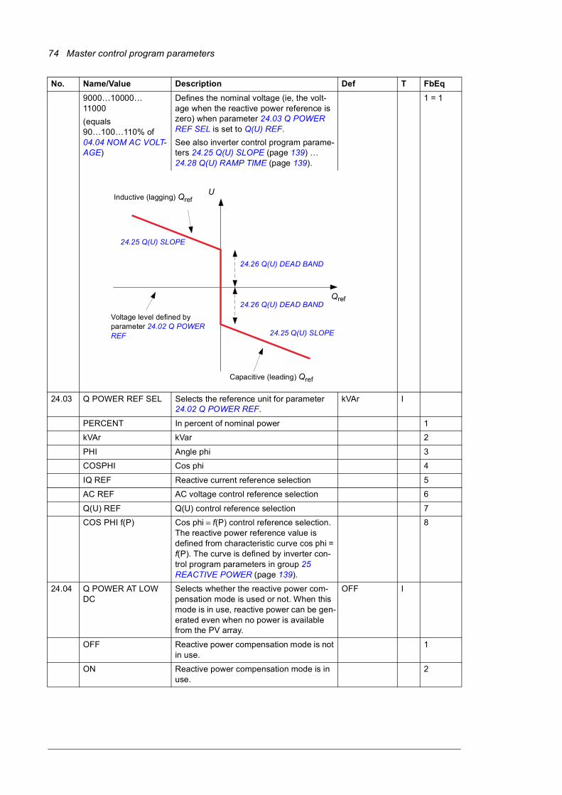
74 Master control program parameters
9000…10000…11000
(equals 90…100…110% of 04.04 NOM AC VOLT-AGE)
Defines the nominal voltage (ie, the volt-age when the reactive power reference is zero) when parameter 24.03 Q POWER REF SEL is set to Q(U) REF.
See also inverter control program parame-ters 24.25 Q(U) SLOPE (page 139) … 24.28 Q(U) RAMP TIME (page 139).
1 = 1
24.03 Q POWER REF SEL Selects the reference unit for parameter 24.02 Q POWER REF.
kVAr I
PERCENT In percent of nominal power 1
kVAr kVar 2
PHI Angle phi 3
COSPHI Cos phi 4
IQ REF Reactive current reference selection 5
AC REF AC voltage control reference selection 6
Q(U) REF Q(U) control reference selection 7
COS PHI f(P) Cos phi = f(P) control reference selection. The reactive power reference value is defined from characteristic curve cos phi = f(P). The curve is defined by inverter con-trol program parameters in group 25 REACTIVE POWER (page 139).
8
24.04 Q POWER AT LOW DC
Selects whether the reactive power com-pensation mode is used or not. When this mode is in use, reactive power can be gen-erated even when no power is available from the PV array.
OFF I
OFF Reactive power compensation mode is not in use.
1
ON Reactive power compensation mode is in use.
2
No. Name/Value Description Def T FbEq
Inductive (lagging) QrefU
Qref
Voltage level defined by parameter 24.02 Q POWER REF
24.25 Q(U) SLOPE
24.26 Q(U) DEAD BAND
24.26 Q(U) DEAD BAND
24.25 Q(U) SLOPE
Capacitive (leading) Qref

Master control program parameters 75
25 DC GROUNDING Parameter group for DC grounding set-tings
25.01 GND MODE SELECT Defines a usage mode of the DC ground-ing.
OFF I
OFF DC grounding control and monitoring are disabled.
0
AUTO DC grounding control and monitoring are enabled.
1
CONT CLOSED DC grounding contactor is manually closed (no monitoring).
Note: This mode is used only for commis-sioning or servicing.
2
CONT OPEN DC grounding contactor is manually open (no monitoring).
3
26 DC INPUT CONFIG DC input current measurement settings
26.01 NR OF DC INPUTS Defines the number of DC inputs. OFF I -
OFF Not in use 0
4 INPUTS 4 inputs 1
5 INPUTS 5 inputs 2
6 INPUTS 6 inputs 3
7 INPUTS 7 inputs 4
8 INPUTS 8 inputs 5
9 INPUTS 9 inputs 6
10 INPUTS 10 inputs 7
11 INPUTS 11 inputs 8
12 INPUTS 12 inputs 9
13 INPUTS 13 inputs 10
14 INPUTS 14 inputs 11
15 INPUTS 15 inputs 12
16 INPUTS 16 inputs 13
26.02 MIN DC CUR DEV Defines the minimum deviation from the average DC input current after which the inverter generates alarm DC INPUT DEV (2185) if the alarm is enabled in parameter 26.06 DC INPUT MODE.
20 A R
0…1000 A Minimum DC current deviation 10 = 1 A
26.03 DC INPUT MASK Defines which DC inputs are included in the DC input current deviation calculation and diagnostics.
• Bit value 1 = The corresponding DC input is included.
• Bit value 0 = The corresponding DC input is not included.
For example, binary value 1100 means that DC inputs 4 and 3 are included in the DC input current deviation calculation and diagnostics, but DC inputs 2 and 1 are not.
0xFFF PB
0x0…0xFFFF DC inputs included in the DC input current deviation calculation and diagnostics
1 = 1
No. Name/Value Description Def T FbEq

76 Master control program parameters
26.04 DC INPUT STATUS Indicates which DC inputs are in order and which DC inputs deviate from the average DC input current. The minimum deviation is defined by parameter 26.02 MIN DC CUR DEV. The deviation must be present, at the minimum, for the duration defined by parameter 26.05 DC CUR DEV DELAY before the inverter generates alarm DC INPUT DEV (2185) and the corresponding status bit is set to 1.
• Bit value 1 = A deviation has occurred in the corresponding DC input.
• Bit value 0 = The corresponding DC input is in order.
For example, binary value 1100 means that a deviation has occurred in DC inputs 3 and 4.
0x0 PB
0x0…0xFFFF DC input status 1 = 1
26.05 DC CUR DEV DELAY Defines for how long DC current can devi-ate from the average DC input current before the inverter generates alarm DC INPUT DEV (2185) and the corresponding status bit in 26.04 DC INPUT STATUS is set to 1.
900 R
0…3600 s DC current deviation delay 10 = 1 s
26.06 DC INPUT MODE Defines whether a deviation in the DC input currents causes alarm DC INPUT DEV (2185) or not.
OFF I
OFF No alarm is generated. 0
ALARM Alarm DC INPUT DEV (2185) is gener-ated.
1
26.07 CUR TRANSDUC SEL Defines the maximum measurable current of the current transducer used in DC input current measurements.
100 A R
0…1000 A Maximum measurable current of the cur-rent transducer
1 = 1 A
28 MAILBOX Mailbox interface
28.01 WRITE ADDRESS Defines the address where the input data will be written to. If the address is greater than 10000, an offset of 10000 is sub-tracted from it, and the result is forwarded to the Inverter control program.
Parameter writing is triggered if there is a non-zero value in this parameter. A zero value is automatically written to this parameter after the execution of parameter writing.
Example: If the address is 2402, the write command will be targeted to Master con-trol program parameter 24.02 Q POWER REF. If the address is 11901, the write command will be targeted to Inverter con-trol program parameter 19.01 DATA 1.
0 I
0…30000 Address to be written. The address format is: (group number * 100) + index number.
1 = 1
No. Name/Value Description Def T FbEq

Master control program parameters 77
28.02 INPUT DATA Defines the value which will be written to the address defined by parameter 28.01 WRITE ADDRESS.
0 I
-32768…32767 Data value 1 = 1
28.03 READ ADDRESS Defines the address where the output data will be read from. If the address is greater than 10000, an offset of 10000 is sub-tracted from it, and the result is forwarded to the Inverter control program.
Example: If the address is 134, the read command will be targeted to Master con-trol program parameter 01.34 PV MOD-ULE DC MEAS. If the address is 10110, the read command will be targeted to Inverter control program parameter 01.10 DC VOLTAGE.
0 I
0…30000 Address to be read. The address format is: (group number * 100) + index number.
1 = 1
28.04 WRITE ADDRESS FB Shows feedback for the write operation:
• Original write address if the write operation was successful
• Zero if the write operation was not successful.
0 I 1 = 1
28.05 OUTPUT DATA Shows the data that is read from the given read address.
Note: If the read operation is not success-ful, the data in this parameter is not valid and it must be discarded.
0 I 1 = 1
28.06 READ ADDRESS FB Shows feedback from the read operation:
• Original read address if the read operation was successful
• Zero if the read operation was not successful.
0 I 1 = 1
30 FAULT FUNCTIONS Programmable protective functions
30.01 DI3 EXT EVENT Selects how the master control program reacts to the “0” state of digital input DI3.
Note: Digital input DI3 is reserved for AC and DC overvoltage protection.
DI3=0 ALARMS
I
NO No action 1
DI3=0 ALARMS If the digital input switches to 0, an alarm is given.
2
DI3=0 FAULTS If the digital input switches to 0, the master control program trips on a fault.
3
30.02 DI4 EXT EVENT Selects how the master control program reacts to the “0” state of digital input DI4.
Note: With option +G420 the digital input DI4 is reserved for DC cable overcurrent protection.
NO I
NO No action 1
DI4=0 ALARMS If the digital input switches to 0, an alarm is given.
2
DI4=0 FAULTS If the digital input switches to 0, the master control program trips on a fault.
3
No. Name/Value Description Def T FbEq

78 Master control program parameters
30.03 DI5 EXT EVENT Selects how the master control program reacts to the “0” state of digital input DI5.
NO I
NO No action 1
DI5=0 ALARMS If the digital input switches to 0, an alarm is given.
2
DI5=0 FAULTS If the digital input switches to 0, the master control program trips on a fault.
3
30.04 RESET DELAY [s] Defines an interval for automatic resets. 60 I
0…32767 s Automatic reset interval 1 = 1 s
30.05 NUMBER OF TRIALS Defines how many automatic resets are attempted.
0 = Automatic reset disabled.
0 I
0…32767 Number of automatic resets 1 = 1
30.06 CURRENT DEV FUNC
Selects the fault function for the detected current deviation used in string box moni-toring.
NO I
NO No specific fault function. The detected current deviation can be seen only in sta-tus words.
0
ALARM Inverter generates alarm BX CUR DEV if a current deviation is detected (X means the number of the communication channel). The detected deviation can also be seen in status words.
1
30.07 CURRENT DEV DELAY
Defines a time delay for the BX CUR DEV alarm. The current deviation must be pres-ent longer than this delay before the alarm is generated.
600 s R
0.5…419430 s Time delay for the BX CUR DEV alarm 10 = 1 s
30.08 SBOX LOST FUNC Selects the fault function for a Modbus link lost.
NO I
NO No specific fault function. The status of the Modbus link can be seen only in status words.
0
ALARM Inverter generates alarm SBOX X LINK if a Modbus link is broken (X in the middle means the number of the communication channel). The status of the link can also be seen in status words.
1
30.09 SBOX LOST DELAY Defines a time delay for the SBOX X LINK alarm. The link lost situation must be pres-ent longer than this delay before the alarm is generated.
60 s R
0.5…419430 s Time delay for the SBOX X LINK alarm 10 = 1 s
30.10 EM STOP FUNCTION Selects how the master control program indicates an open emergency stop circuit. The status of the emergency stop circuit is shown in digital input 6.
FAULT I
NO No alarm indication 1
No. Name/Value Description Def T FbEq

Master control program parameters 79
ALARM Alarm EM STOP (F081) is created.
The alarm is active if:
• Status of digital input 6 (DI6) = 0
• 20-second power-up-delay has elapsed
• 30.10 EM STOP FUNCTION = ALARM.
2
FAULT Fault EM STOP (F083) is created.
The fault is active if:
• Status of digital input 6 (DI6) = 0
• 20-second power-up-delay has elapsed
• 30.10 EM STOP FUNCTION = FAULT.
3
30.11 AUTO RESET MASK Defines a mask for excluding certain faults from the automatic fault reset function. All other faults are reset by the automatic fault reset function if it is enabled.
Bit value 1 means that the fault is reset by the automatic fault reset function and 0 means that the fault is not reset by auto-matic fault reset function.
0x03 PB 1 = 1
31 PVA CONTROL Various master control program settings
31.01 ENABLE MPPT Enables/disables the operation of the PVS800.
0 = Force state of PVS800 to STAND BY.
See also section PVS800 state machine on page 31.
C.00001 P
-255.255.31 … +255.255.31 /
C. -32768 … C. 32767
Parameter pointer or a constant value:
• Parameter pointer: Inversion, group, index and bit fields. Bit number is effective only for blocks handling Boolean inputs.
• Constant value: Inversion and constant fields. Inversion field must have value C to enable the constant setting.
31.03 UDC MAX SCALE Defines the DC voltage that corresponds to the DC measurement source signal value of 20000.
1200 V R
0…2000 V Value 1 = 1 V
31.04 UDC START LIM Defines a start limit for the inverter. When the DC voltage exceeds this limit (and the master control program is started), the inverter is started.
600 V R
450…2000 V Start DC limit 1 = 1 V
31.05 UDC START DLY Defines a delay for parameter 31.04 UDC START LIM; the DC voltage must stay above the start limit for longer than the delay before the inverter is started.
10 min R
0.0…10000.0 min Delay for start DC limit 1 = 1 min
No. Name/Value Description Def T FbEq
Bit 0 External grid monitoring fault (from the grid monitoring relay)
Bit 1 Insulation resistance fault

80 Master control program parameters
31.06 UDC STOP LIM Defines a sleep limit for the inverter. When the DC voltage falls below this limit, the inverter is stopped.
If parameter 31.22 UDC STOP LIM AUTO = ENABLED, the value of this parameter is automatically updated based on the mea-sured grid voltage.
450 V R
0…2000 V Stop DC limit 1 = 1 V
31.07 UDC STOP DLY Defines a delay for parameter 31.06 UDC STOP LIM; the DC voltage must stay below the sleep limit for longer than the delay before the inverter is stopped.
30 min R
0.0…10000.0 min Value 1 = 1 min
31.09 POWER SOURCE Defines the signal source that is used by the master control program state machine to determine output power.
Default setting is the power measured by, and received from, the inverter unit (parameter 01.11 AC POWER).
+.001.011.00 P
-255.255.31 … +255.255.31 /
C. -32768 … C. 32767
Parameter pointer or a constant value:
• Parameter pointer: Inversion, group, index and bit fields. Bit number is effective only for blocks handling Boolean inputs.
• Constant value: Inversion and constant fields. Inversion field must have value C to enable the constant setting.
31.10 POWER STOP LIM Defines a stop limit for the inverter unit. When the output power falls below this limit, the inverter unit is stopped.
Value of 10000 corresponds to the nominal power of the inverter unit. See also parameter 31.16 POWER LIMITING.
150 I
0…20000 Output power stop limit 1 = 1
31.11 POWER STOP DLY Defines a delay for parameter 31.10 POWER STOP LIM; the output power must stay below the stop limit for longer than the delay before the inverter unit is stopped.
30 min R
0.0…10000.0 min Output power stop delay 1 = 1 min
31.12 GOTO SLEEP MODE Defines which conditions must be true for the master control program to enter the sleep mode.
UDC OR POW
I
UDC AND POW PVS800 will enter the sleep mode when both the DC voltage and output power are under their respective stop limits (and remain there until any stop delays elapse).
1
UDC OR POW PVS800 will enter the sleep mode when either the DC voltage or output power is under its respective stop limit (and remains there until the stop delay elapses).
2
No. Name/Value Description Def T FbEq

Master control program parameters 81
31.13 WAKE UP SOURCE Selects a source that can be used to wake up the PVS800.
When the value of the monitored source exceeds the limit set by parameter 31.14 WAKE UP START LIM, and remains there until the delay set by 31.15 WAKE UP START DLY elapses, the inverter unit is started (provided that the conditions for the DC voltage, defined by other parameters in this group, are fulfilled).
If no wake-up source is needed, leave parameters 31.13…31.15 at their default (zero) settings.
+.000.000.00 P
-255.255.31 … +255.255.31 /
C. -32768 … C. 32767
Parameter pointer or a constant value:
• Parameter pointer: Inversion, group, index and bit fields. Bit number is effective only for blocks handling Boolean inputs.
• Constant value: Inversion and constant fields. Inversion field must have value C to enable the constant setting.
31.14 WAKE UP START LIM Defines a wake-up limit for the signal selected by parameter 31.13 WAKE UP SOURCE.
0 I
0…20000 Wake-up limit 1 = 1
31.15 WAKE UP START DLY Defines a wake-up delay for parameter 31.13 WAKE UP SOURCE.
0 min R
0.0…10000.0 min Wake-up start delay 1 = 1
31.16 POWER LIMITING Defines an external active power limit of PVS800 in percent of nominal power (parameter 04.06 NOM AC POWER) of the inverter unit.
If the value of parameter 31.16 POWER LIMITING is smaller than the value of parameter 31.10 POWER STOP LIM, the inverter goes to Sleep mode.
200% R
0…200% Active power limit 100 = 1%
31.17 CELL TEMP COEFF Parameters 31.17…31.19 define a photo-voltaic cell temperature correction that is applied to the DC voltage start level.
Defines a temperature coefficient for the open-loop solar cell voltage. If set to zero, no temperature correction is applied.
Coefficient must be given for a complete photovoltaic string.
0 V/K R
-5…0 V/K Cell temperature coefficient 100 = 1 V/K
31.18 CELL TEMP COR LIM Limit for the effect of the temperature cor-rection function.
Base value for the DC voltage start level is read from parameter 31.04 UDC START LIM.
3% R
0…10% Temperature correction limit 100 = 1%
No. Name/Value Description Def T FbEq
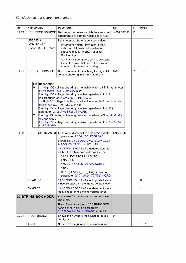
82 Master control program parameters
31.19 CELL TEMP SOURCE Defines a source from which the measured temperature of a photovoltaic cell is read.
+.001.037.00 P
-255.255.31 … +255.255.31 /
C. -32768 … C. 32767
Parameter pointer or a constant value:
• Parameter pointer: Inversion, group, index and bit fields. Bit number is effective only for blocks handling Boolean inputs.
• Constant value: Inversion and constant fields. Inversion field must have value C to enable the constant setting.
31.21 UDC HIGH DISABLE Defines a mask for disabling the high DC voltage checking in certain situations.
0x03 PB 1 = 1
31.22 UDC STOP LIM AUTO Enables or disables the automatic update of parameter 31.06 UDC STOP LIM.
If enabled, 31.06 UDC STOP LIM = 02.03 MAINS VOLTAGE x sqrt(2) + 15 V.
31.06 UDC STOP LIM is updated automat-ically if the following conditions are met:
• 31.22 UDC STOP LIM AUTO = ENABLED
• 200 V < 02.03 MAINS VOLTAGE < 450 V
• Bit 11 (LEVEL1_DIP_STA) is clear in parameter 08.01 MAIN STATUS WORD.
ENABLED
DISABLED 31.06 UDC STOP LIM is not updated auto-matically based on the mains voltage level.
0
ENABLED 31.06 UDC STOP LIM is updated automat-ically based on the mains voltage level.
1
32 STRING BOX ADDR Addresses for junction box communication channels.
Note: Parameter group 32 STRING BOX ADDR is not visible if parameter 33.01ENABLE MONITORING = FALSE.
32.01 NR OF BOXES Shows the number of the junction boxes configured.
0 I
0…20 Number of the junction boxes configured 1 = 1
No. Name/Value Description Def T FbEq
Bit Description0 1 = High DC voltage checking is not active when bit 11 in parameter
08.01 MAIN STATUS WORD is set.0 = High DC voltage checking is active regardless of bit 11 in parameter 08.01 MAIN STATUS WORD.
1 1= High DC voltage checking is not active when bit 11 in parameter 08.05 PVA STATUS WORD is set.0 = High DC voltage checking is active regardless of bit 11 in parameter 08.05 PVA STATUS WORD.
2 1 = High DC voltage checking is not active when bit 9 in 08.08 LIMIT WORD is set.0 = High DC voltage checking is active regardless of bit 9 in 08.08 LIMIT WORD.

Master control program parameters 83
32.03 BOX1 NODE ADDR Defines the address for junction box com-munication channel 1. Zero address means that the communication channel is not configured and, thus, not used.
0 I
0…247 Address for communication channel 1 1 = 1
32.04 BOX2 NODE ADDR Defines an address for junction box com-munication channel 2. Zero address means that the communication channel is not configured and, thus, not used.
0 I
0…247 Address for communication channel 2 1 = 1
… … … … … …
32.22 BOX20 NODE ADDR Defines an address for junction box com-munication channel 20. Zero address means that the communication channel is not configured and, thus, not used.
0 I
0…247 Address for communication channel 20 1 = 1
33 STRING MON SET Settings for string monitoring
33.01 ENABLE MONITORING
Enables communication for string monitor-ing.
• If the communication is enabled, the master control unit cyclically polls the configured junction boxes.
• If the communication is disabled, the master control unit does not communicate with the junction boxes.
FALSE B
FALSE String monitoring is disabled. 0
TRUE String monitoring is enabled. 1
33.02 CUR DEV CALC ENA Enables current deviation calculation. String monitoring (see parameter 33.01) must be enabled to receive the measured currents from the junction boxes.
FALSE B
FALSE Current deviation calculation is disabled. 0
TRUE Current deviation calculation is enabled. 1
33.03 MIN CUR DEVIATION Defines the minimum current deviation for a status indication. If the difference between an average string current and a single string current is bigger than this set-ting, a deviation is noticed and the corre-sponding bit in parameters 36.01 BOX1 CUR DEV STA…36.20 BOX20 CUR DEV STA is set. Average string current is calcu-lated separately in each junction box from all enabled strings.
1 A R
0…1000 A Minimum current deviation for a status indication
1000 = 1 A
33.04 MB MASTER CYCLE Defines the time between two master requests (polls) in cyclical communication. Time to poll all the configured junction boxes is then (33.04 MB MASTER CYCLE) x (32.01 NR OF BOXES).
1 s R
0.2…1000 s Modbus master cycle time 100 = 1 s
No. Name/Value Description Def T FbEq

84 Master control program parameters
33.05 MB MASTER TIMEOUT
Defines a time-out for Modbus master requests. If the response for the master's request is not received within this time, the communication link is considered broken. Time-out counting is started when the request is sent from the Modbus master to the junction box.
0.3 s R
0.2…1000 s Modbus master time-out 100 = 1 s
33.06 MODBUS MODE Selects the Modbus mode (master or slave) for the RMBA-01 module installed into RMIO slot 2. If the string monitoring function is used, this parameter must be set to MASTER.
SLAVE
SLAVE RMBA-01 is used in the slave mode. 0
MASTER RMBA-01 is used in the master mode. 1
33.07 ACYC REQUEST MODE
Selects the type of the acyclical request. When the request is sent, it is either a read request or a write request. Only one regis-ter value is read or written within the request.
READ VALUE B
READ VALUE Read request will be sent to the junction box.
0
WRITE VALUE Write request will be sent to the junction box.
1
33.08 REQUEST NODE ADDR
Defines the station address where the acy-clical request is sent.
0 I
0…247 Station address in the request. Address of 0 means a broadcast message; it should be used only in the write mode.
1 = 1
33.09 REQUEST REG ADDR
Defines the register address to be read or to be written. Writing a value to this param-eter triggers sending of the acyclical request.
0 I
1…9999 Register address 1 = 1
33.10 ACYCLIC DATA Defines or shows the data in acyclical communication.
This parameter has three purposes:
• If parameter 33.07 ACYC REQUEST MODE is set to WRITE VALUE, this parameter defines the data that is written to a junction box register.
• If parameter 33.07 ACYC REQUEST MODE is set to READ VALUE, this parameter shows the data that is read from a junction box register.
• If the Modbus master receives an error response, this parameter shows the exception code in the error response.
0
-32768…32767 Data in acyclical communication 1 = 1
No. Name/Value Description Def T FbEq

Master control program parameters 85
34 STRING MON STAT Status words for string monitoring
34.01 LINK STATUS 1-16 Shows the Modbus link status for commu-nication channels 1…16.
0 PB
Bit 0 is for the 1st communication channel, bit 1 is for the 2nd communication channel … and bit 15 is for the 16th communication channel
0…65535 1 = 1
34.02 LINK STATUS 17-20 Shows the Modbus link status for commu-nication channels 17…20.
0 PB
Bit 0 is for the 17th communication chan-nel, bit 1 is for the 18th communication channel … and bit 3 is for the 20th commu-nication channel.
0…15 1 = 1
34.03 MONITORING STATUS
Status word for string monitoring. 0
0…15 1 = 1
No. Name/Value Description Def T FbEq
Bit Value Information0…15 1 Link is OK; Modbus master is communicating with the junction box.
0 Link is broken; Modbus master cannot communicate with the junction box. Either the communication channel is not configured in parameter group 32 or there is a communication break.
Bit Value Information0…3 1 Link is OK; Modbus master is communicating with the junction box.
0 Link is broken; Modbus master cannot communicate with the junction box. Either the communication channel is not configured in parameter group 32 or there is a communication break.
Bit Value Information0 1 String monitoring is enabled.
0 String monitoring is disabled.1 1 Current deviation calculation is enabled.
0 Current deviation calculation is disabled.2 1 RMBA-01 is in the master mode.
0 RMBA-01 is in the slave mode.3 1 Write mode is selected for acyclical communication.
0 Read mode is selected for acyclical communication.

86 Master control program parameters
34.04 ACYC REQUEST STAT
Status word for acyclical communication.
Status word during a successful acyclical request:
0x0001 (request sending is triggered)-> 0x0002 (request is sent)-> 0x0000 (a successful response).
Bits 0, 2 and 3 are cleared when a request is sent. Bit 1 is cleared when an OK response is detected. Successful acyclical communication can be tested by compar-ing the request status word against a zero value.
0
0…31 1 = 1
34.05 MB OK MSG CNT Shows the number of OK messages received by the Modbus master since the last power-up.
0 PB
0…65535 1 = 1
34.06 MB ERR MSG CNT Shows the number of error messages received by the Modbus master since the last power-up.
0 PB
0…65535 1 = 1
34.07 MB TIMEOUT CNT Shows the number of the Modbus master requests that have ended to a time-out since the last power-up.
0 PB
0…65535 1 = 1
No. Name/Value Description Def T FbEq
Bit Value Information0 1 Request sending is triggered; the request will be sent when the communica-
tion bus is idle.0 No messages are waiting for to be sent.
1 1 Request is sent; the master is waiting for a response.0 Request processing is not active.
2 1 Time-out counter has expired (no response from the junction box).0 Time-out counter has not expired.
3 1 There was an exception code in the response from a junction box. Code is shown in parameter 33.10.
0 Response message from a junction box was successful (no exception code).
4 1 Input data in parameter 33.08 or 33.09 is invalid. Acyclical request is not sent.
0 Input data in parameters 33.08 and 33.09 was valid when the message sending process was triggered.

Master control program parameters 87
34.08 CUR DEV STA 1-16 Shows the current deviation status word for junction box communication channels 1…16.
Bit 0 is for the 1st communication channel, bit 1 is for the 2nd communication channel … and bit 15 is for the 16th communication channel.
0 PB
0…65535 1 = 1
34.09 CUR DEV STA 17-20 Shows the current deviation status word for junction box communication channels 17…20.
Bit 0 is for the 17th communication chan-nel, bit 1 is for the 18th communication channel … and bit 3 is for the 20th commu-nication channel.
0 PB
0…15 1 = 1
35 ENABLED STRINGS Strings that are part of current monitoring.
Note: Parameter group 35 ENABLED STRINGS is not visible if parameter 33.01ENABLE MONITORING = FALSE.
35.01 BOX1 STRING ENA Defines which strings are enabled in junc-tion box 1. One bit corresponds to one string in junction box channel 1.
Bit 0 is for the 1st string, bit 1 is for the 2nd string … and bit 7 is for the 8th string.
65535 =0xFFFF
PB
0…255 Enabled strings in decimal format 1 = 1
No. Name/Value Description Def T FbEq
Bit Value Information0…15 1 Current deviation is
detected.0 Current deviation is not
detected.
Bit Value Information0…3 1 Current deviation is
detected.0 Current deviation is not
detected.
Bit Value Information0…7 1 String channel is enabled
in string monitoring and current deviation calcula-tion.
0 String channel is disabled in string monitoring and current deviation calcula-tion.

88 Master control program parameters
35.02 BOX2 STRING ENA Defines which strings are enabled in junc-tion box 2. One bit corresponds to one string in junction box channel 2.
Bit 0 is for the 1st string, bit 1 is for the 2nd string … and bit 7 is for the 8th string.
65535 =0xFFFF
PB
0…255 Enabled strings in decimal format 1 = 1
… … … … … …
35.20 BOX20 STRING ENA Defines which strings are enabled in junc-tion box 20. One bit corresponds to one string in junction box channel 20.
Bit 0 is for the 1st string, bit 1 is for the 2nd string … and bit 7 is for the 8th string.
65535 =0xFFFF
PB
0…255 Enabled strings in decimal format 1 = 1
36 SBOX CUR DEV STA String current deviation status information.
Note: Parameter group 36 SBOX CUR DEV STA is not visible if parameter 33.01ENABLE MONITORING = FALSE.
36.01 BOX1 CUR DEV STA Shows the status of string current devia-tions in junction box communication chan-nel 1.
Bit 0 is for the 1st string, bit 1 is for the 2nd string … and bit 7 is for the 8th string.
0 PB
0…255 1 =1
No. Name/Value Description Def T FbEq
Bit Value Information0…7 1 String channel is enabled
in string monitoring and current deviation calcula-tion.
0 String channel is disa-bled in string monitoring and current deviation cal-culation.
Bit Value Information0…7 1 String channel is enabled
in string monitoring and current deviation calcula-tion.
0 String channel is disabled in string monitoring and current deviation calcula-tion.
Bit Value Information0…7 1 Current deviation is
detected.0 Current deviation is not
detected.

Master control program parameters 89
36.02 BOX2 CUR DEV STA Shows the status of string current devia-tions in junction box communication chan-nel 2.
Bit 0 is for the 1st string, bit 1 is for the 2nd string … and bit 7 is for the 8th string.
0 PB
0…255 1 = 1
… … … … … …
36.20 BOX20 CUR DEV STA Shows the status of string current devia-tions in junction box communication chan-nel 20.
Bit 0 is for the 1st string, bit 1 is for the 2nd string … and bit 7 is for the 8th string.
0 PB
0…255 1 = 1
40 STRING BOX 1 & 2 Actual signals read from communication channels 1 and 2 (ie, junction boxes 1 and 2) using cyclical communication. Signals 40.01…40.27 are for junction box 1 and signals 40.36…40.62 are for junction box 2.
Note: Parameter group 40 STRING BOX 1 & 2 is not visible if parameter 33.01ENABLE MONITORING = FALSE.
40.01 BOX1 TYPE Shows the junction box type (example: 0x040B).
0 PB 1 = 1
40.02 BOX1 SW VERSION Shows the software version (example: 0x102A).
0 PB 1 = 1
40.03 BOX1 HW VERSION Shows the hardware version (example: 0x0102).
0 PB 1 = 1
40.04 BOX1 NR OF CHAN Shows the number of the current measure-ment channels.
0 I 1 = 1
40.05 BOX1 RESERVED D5 Shows the status of the string monitoring unit.
0 I 1 = 1
40.06 BOX1 RESERVED D6 Reserved 0 I 1 = 1
40.07 BOX1 OK MSG CNT Shows the number of OK messages. 0 PB 1 = 1
40.08 BOX1 ER MSG CNT Shows the number of error messages. 0 PB 1 = 1
No. Name/Value Description Def T FbEq
Bit Value Information0…7 1 Current deviation is
detected.0 Current deviation is not
detected.
Bit Value Information0…7 1 Current deviation is
detected.0 Current deviation is not
detected.
0x0001 Normal mode, initialization0x0002 Normal mode, running0x0003 Normal mode, error0x0100 Calibration mode, initialization0x0200 Calibration mode, running0x0300 Calibration mode, error0x0400 Calibration mode has ended

90 Master control program parameters
40.09 BOX1 BOARD TEMP Shows the temperature of the string moni-toring unit.
0 R 10 = 1°C
40.10 ANALOG INPUT 1 Shows the measured current/voltage in analog input 1.
0 I 50 = 1 mA or100 = 1 V
40.11 ANALOG INPUT 2 Shows the measured current/voltage in analog input 2.
0 I 2 = 1 mV
40.12 PT100 TEMP A Shows the measured temperature in Pt100 channel A.
0 I 10 = 1°C
40.13 PT100 TEMP B Shows the measured temperature in Pt100 channel B.
0 I 10 = 1°C
40.14 RESERVED D14 Reserved 0
40.15 DI STATUS WORD Shows the status of the digital inputs. 0 PB 1 = 1
40.16 RESERVED D16 Reserved
40.17 RESERVED D17 Reserved
40.18 RESERVED D18 Reserved
40.19 RESERVED D19 Reserved
40.20 STRING 1 AVG CUR Shows the average current of string 1. 0 R 1000 =1 A
40.21 STRING 2 AVG CUR Shows the average current of string 2. 0 R 1000 =1 A
… … … … … …
40.35 STRING 16 AVG CUR Shows the average current of string 16. 0 R 1000 =1 A
40.36 BOX2 TYPE Shows the junction box type (example: 0x040B).
0 PB 1 = 1
40.37 BOX2 SW VERSION Shows the software version (example: 0x102A).
0 PB 1 = 1
40.38 BOX2 HW VERSION Shows the hardware version (example: 0x0102).
0 PB 1 = 1
40.39 BOX2 NR OF CHAN Shows the number of the current measure-ment channels.
0 I 1 = 1
40.40 BOX2 RESERVED D5 Shows the status of the string monitoring unit.
1 = 1
40.41 BOX2 RESERVED D6 Reserved
40.42 BOX2 OK MSG CNT Shows the number of OK messages. 0 PB 1 = 1
40.43 BOX2 ER MSG CNT Shows the number of error messages. 0 PB 1 = 1
40.44 BOX2 BOARD TEMP Shows the temperature of the string moni-toring unit.
0 R 10 = 1°C
No. Name/Value Description Def T FbEq
Bit 1 Status of digital input 1Bit 2 Status of digital input 2Bit 3 Status of digital input 3
0x0001 Normal mode, initialization0x0002 Normal mode, running0x0003 Normal mode, error0x0100 Calibration mode, initialization0x0200 Calibration mode, running0x0300 Calibration mode, error0x0400 Calibration mode has ended
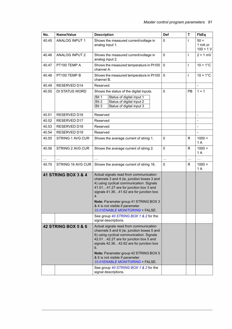
Master control program parameters 91
40.45 ANALOG INPUT 1 Shows the measured current/voltage in analog input 1.
0 I 50 =1 mA or100 = 1 V
40.46 ANALOG INPUT 2 Shows the measured current/voltage in analog input 2.
0 I 2 = 1 mV
40.47 PT100 TEMP A Shows the measured temperature in Pt100 channel A.
0 I 10 = 1°C
40.48 PT100 TEMP B Shows the measured temperature in Pt100 channel B.
0 I 10 = 1°C
40.49 RESERVED D14 Reserved -
40.50 DI STATUS WORD Shows the status of the digital inputs. 0 PB 1 = 1
40.51 RESERVED D16 Reserved -
40.52 RESERVED D17 Reserved -
40.53 RESERVED D18 Reserved -
40.54 RESERVED D19 Reserved -
40.55 STRING 1 AVG CUR Shows the average current of string 1. 0 R 1000 =1 A
40.56 STRING 2 AVG CUR Shows the average current of string 2. 0 R 1000 =1 A
… … … … … …
40.70 STRING 16 AVG CUR Shows the average current of string 16. 0 R 1000 =1 A
41 STRING BOX 3 & 4 Actual signals read from communication channels 3 and 4 (ie, junction boxes 3 and 4) using cyclical communication. Signals 41.01…41.27 are for junction box 3 and signals 41.36…41.62 are for junction box 4.
Note: Parameter group 41 STRING BOX 3 & 4 is not visible if parameter 33.01ENABLE MONITORING = FALSE.
See group 40 STRING BOX 1 & 2 for the signal descriptions.
42 STRING BOX 5 & 6 Actual signals read from communication channels 5 and 6 (ie, junction boxes 5 and 6) using cyclical communication. Signals 42.01…42.27 are for junction box 5 and signals 42.36…42.62 are for junction box 6.
Note: Parameter group 42 STRING BOX 5 & 6 is not visible if parameter 33.01ENABLE MONITORING = FALSE.
See group 40 STRING BOX 1 & 2 for the signal descriptions.
No. Name/Value Description Def T FbEq
Bit 1 Status of digital input 1Bit 2 Status of digital input 2Bit 3 Status of digital input 3

92 Master control program parameters
43 STRING BOX 7 & 8 Actual signals read from communication channels 7 and 8 (ie, junction boxes 7 and 8) using cyclical communication. Signals 43.01…43.27 are for junction box 7 and signals 43.36…43.62 are for junction box 8.
Note: Parameter group 43 STRING BOX 7 & 8 is not visible if parameter 33.01ENABLE MONITORING = FALSE.
See group 40 STRING BOX 1 & 2 for the signal descriptions.
44 STRING BOX 9 & 10 Actual signals read from communication channels 9 and 10 (ie, junction boxes 9 and 10) using cyclical communication. Sig-nals 44.01…44.27 are for junction box 9 and signals 44.36…44.62 are for junction box 10.
Note: Parameter group 44 STRING BOX 9 & 10 is not visible if parameter 33.01ENABLE MONITORING = FALSE.
See group 40 STRING BOX 1 & 2 for the signal descriptions.
45 STRING BOX 11 & 12 Actual signals read from communication channels 11 and 12 (ie, junction boxes 11 and 12) using cyclical communication. Sig-nals 45.01…45.27 are for junction box 11 and signals 45.36…45.62 are for junction box 12.
Note: Parameter group 45 STRING BOX 11 & 12 is not visible if parameter 33.01ENABLE MONITORING = FALSE.
See group 40 STRING BOX 1 & 2 for the signal descriptions.
46 STRING BOX 13 & 14 Actual signals read from communication channels 13 and 14 (ie, junction boxes 13 and 14) using cyclical communication. Sig-nals 46.01…46.27 are for junction box 13 and signals 46.36…46.62 are for junction box 14.
Note: Parameter group 46 STRING BOX 13 & 14 is not visible if parameter 33.01ENABLE MONITORING = FALSE.
See group 40 STRING BOX 1 & 2 for the signal descriptions.
47 STRING BOX 15 & 16 Actual signals read from communication channels 15 and 16 (ie, junction boxes 15 and 16) using cyclical communication. Sig-nals 47.01…47.27 are for junction box 15 and signals 47.36…47.62 are for junction box 16.
Note: Parameter group 47 STRING BOX 15 & 16 is not visible if parameter 33.01ENABLE MONITORING = FALSE.
See group 40 STRING BOX 1 & 2 for the signal descriptions.
No. Name/Value Description Def T FbEq

Master control program parameters 93
48 STRING BOX 17 & 18 Actual signals read from communication channels 17 and 18 (ie, junction boxes 17 and 18) using cyclical communication. Sig-nals 48.01…48.27 are for junction box 17 and signals 48.36…48.62 are for junction box 18.
Note: Parameter group 48 STRING BOX 17 & 18 is not visible if parameter 33.01ENABLE MONITORING = FALSE.
See group 40 STRING BOX 1 & 2 for the signal descriptions.
49 STRING BOX 19 & 20 Actual signals read from communication channels 19 and 20 (ie, junction boxes 19 and 20) using cyclical communication. Sig-nals 49.01…49.27 are for junction box 19 and signals 49.36…49.62 are for junction box 20.
Note: Parameter group 49 STRING BOX 19 & 20 is not visible if parameter 33.01ENABLE MONITORING = FALSE.
See group 40 STRING BOX 1 & 2 for the signal descriptions.
50 MASTER ADAPTER N
These parameters are visible and need to be adjusted only when an Nxxx type field-bus adapter module (optional) is installed. For details on the parameters, refer to the manual of the adapter module.
Note: Any changes in these parameters take effect only after the next power-up of the adapter module.
50.01 MODULE N TYPE Module type and software version.
NOT DEFINED = No module present.
50.02…50.99
- According to the module type
51 MASTER ADAPTER These parameters are visible and need to be adjusted only when a Rxxx type field-bus adapter module (optional) is installed. For details on the parameters, refer to the manual of the adapter module.
Note: Any changes in these parameters take effect only after the next power-up of the adapter module.
51.01 MODULE TYPE Module type and software version.
NOT DEFINED = No module present.
51.02…51.99
- According to the module type
No. Name/Value Description Def T FbEq
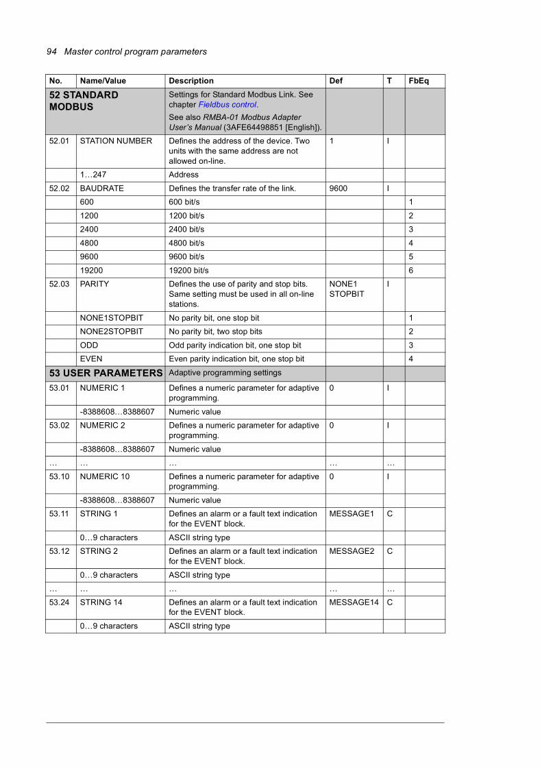
94 Master control program parameters
52 STANDARD MODBUS
Settings for Standard Modbus Link. See chapter Fieldbus control.
See also RMBA-01 Modbus Adapter User’s Manual (3AFE64498851 [English]).
52.01 STATION NUMBER Defines the address of the device. Two units with the same address are not allowed on-line.
1 I
1…247 Address
52.02 BAUDRATE Defines the transfer rate of the link. 9600 I
600 600 bit/s 1
1200 1200 bit/s 2
2400 2400 bit/s 3
4800 4800 bit/s 4
9600 9600 bit/s 5
19200 19200 bit/s 6
52.03 PARITY Defines the use of parity and stop bits. Same setting must be used in all on-line stations.
NONE1STOPBIT
I
NONE1STOPBIT No parity bit, one stop bit 1
NONE2STOPBIT No parity bit, two stop bits 2
ODD Odd parity indication bit, one stop bit 3
EVEN Even parity indication bit, one stop bit 4
53 USER PARAMETERS Adaptive programming settings
53.01 NUMERIC 1 Defines a numeric parameter for adaptive programming.
0 I
-8388608…8388607 Numeric value
53.02 NUMERIC 2 Defines a numeric parameter for adaptive programming.
0 I
-8388608…8388607 Numeric value
… … … … …
53.10 NUMERIC 10 Defines a numeric parameter for adaptive programming.
0 I
-8388608…8388607 Numeric value
53.11 STRING 1 Defines an alarm or a fault text indication for the EVENT block.
MESSAGE1 C
0…9 characters ASCII string type
53.12 STRING 2 Defines an alarm or a fault text indication for the EVENT block.
MESSAGE2 C
0…9 characters ASCII string type
… … … … …
53.24 STRING 14 Defines an alarm or a fault text indication for the EVENT block.
MESSAGE14 C
0…9 characters ASCII string type
No. Name/Value Description Def T FbEq

Master control program parameters 95
55 ADAPTIVE PROG1 Adaptive program task 1 settings:
• selections of the function blocks and their input connections
• diagnostics.
This parameter group is mainly used with adaptive programming. See section Adaptive programming with DriveAP 2.x (page 48) and Application guide: Adaptive program for PVS800 central inverters (3AUA0000091276 [English]).
55.01 STATUS Shows the value of the adaptive program task 1 status word.
0 I
0…15 Table below shows the alternative bit states and the corresponding values on the control panel display.
If all the bits are FALSE (ie, 0), the state is STOPPED.
55.02 FAULTED PAR Points out the faulted parameter in adap-tive program task 1.
0 P
-255.255.31 … +255.255.31
Parameter pointer: Inversion, group, index and bit fields
55.05 BLOCK1 Selects the function block type for block 1 in adaptive program task 1.
NO I
0…32768 Function block type
55.06 INPUT1 Selects the source for input 1 of block 1. 0 P
-255.255.31 … +255.255.31 /
C. -32768 … C. 32767
Parameter index or a constant value:
• Parameter pointer: Inversion, group, index and bit fields. Bit number is effective only for blocks handling Boolean inputs.
• Constant value: Inversion and constant fields. Inversion field must have value C to enable the constant setting.
Example: The state of digital input DI2 is connected to input 1 as follows:
• Set this parameter to +08.02.02. (The adaptive program stores the state of digital input DI2 to bit 2 of actual signal 08.02.)
• If you need an inverted value, switch the sign of the pointer value (-08.02.02).
55.07 INPUT2 Selects the source for input 2 of block 1. 0 P
See parameter 55.06 INPUT1.
55.08 INPUT3 Selects the source for input 3 of block 1. 0 P
See parameter 55.06 INPUT1.
55.09 OUTPUT Stores and displays the output of block 1. 0 I
No user setting possible
No. Name/Value Description Def T FbEq
Bit Display Meaning0 1 Running1 2 Editing2 4 Checking3 8 Faulted

96 Master control program parameters
55.10 BLOCK2 Selects the function block type for block 2 in adaptive program task 1.
NO I
0…32768 Function block type
55.11 INPUT1 Selects the source for input 1 of block 2. 0 P
See parameter 55.06 INPUT1.
55.12 INPUT2 Selects the source for input 2 of block 2. 0 P
See parameter 55.06 INPUT1.
55.13 INPUT3 Selects the source for input 3 of block 2. 0 P
See parameter 55.06 INPUT1.
55.14 OUTPUT Stores and displays the output of block 2. 0 I
No user setting possible
55.15 BLOCK3 Selects the function block type for block 3 in adaptive program task 1.
NO I
0…32768 Function block type
… … … … …
55.54 OUTPUT Stores and displays the output of block 10. 0 I
No user setting possible
56 ADAPT PROG1 CTRL
Adaptive program task 1 control. The update time of task 1 control is 10 ms. This parameter group is mainly used with the DriveAP 2.x PC tool.
See parameter group 55 ADAPTIVE PROG1.
56.01 ADAPT PROG CMD Selects the operation mode for adaptive program task 1.
EDIT I
STOP Stopped. The program cannot be edited. 1
START Running. The program cannot be edited. 2
EDIT Stops to edit the mode (ie, the execution of the task is stopped for editing). The pro-gram can be edited.
3
56.02 EDIT CMD Selects the command for the block placed in the location defined by parameter 56.03 EDIT BLOCK.
NO I
NO Home value. The value automatically reverts to NO after an editing command is executed.
The program must be in the edit mode (see parameter 56.01 ADAPT PROG CMD).
1
PUSH Shifts the block in the location defined by parameter 56.03 EDIT BLOCK and the subsequent blocks one location up. A new block can be placed in the emptied loca-tion.
The program must be in the edit mode (see parameter 56.01 ADAPT PROG CMD).
2
No. Name/Value Description Def T FbEq

Master control program parameters 97
DELETE Selects the block in the location defined by parameter 56.03 EDIT BLOCK and shifts the subsequent blocks one step down.
The program must be in the edit mode (see parameter 56.01 ADAPT PROG CMD).
3
PROTECT Activation of the task protection: Read pro-tects the input connections of the blocks. Activate as follows:
- Ensure the task operation mode is set to START or STOP (parameter 56.01 ADAPT PROG CMD).
- Set the passcode by parameter 56.05 PASSCODE.
- Set this parameter to PROTECT.
When protection is activated:
- All parameters in group 55 ADAPTIVE PROG1 excluding the block output param-eters are hidden (read protected).
- It is not possible to switch the task operat-ing mode (parameter 56.01 ADAPT PROG CMD) to the edit mode.
- Parameter 56.05 PASSCODE is set to 0.
4
UNPROTECT Deactivation of the task protection: no read protection of the inputs of the blocks. Deactivate as follows:
- Ensure the task operation mode is set to START or STOP (parameter 56.01 ADAPT PROG CMD).
- Set the passcode by parameter 56.05 PASSCODE.
- Set this parameter to UNPROTECT.
5
56.03 EDIT BLOCK Defines the block location number for the command selected by parameter 56.02 EDIT CMD.
0 I
1…15 Block location number
56.04 TIMELEV_SEL Indicates the fixed execution cycle time (10 ms) of adaptive program task 1. Also digi-tal and analog inputs are read on this time level.
10ms I
56.05 PASSCODE Defines the passcode, which acti-vates/deactivates the protection of the input connections of the blocks. See parameter 56.02 EDIT CMD.
0 I
0 h…FFFFFF h Passcode. The setting reverts to 0 after the protection is activated/deactivated.
Note: When you activate the protection, write down the passcode and store it for later use.
No. Name/Value Description Def T FbEq
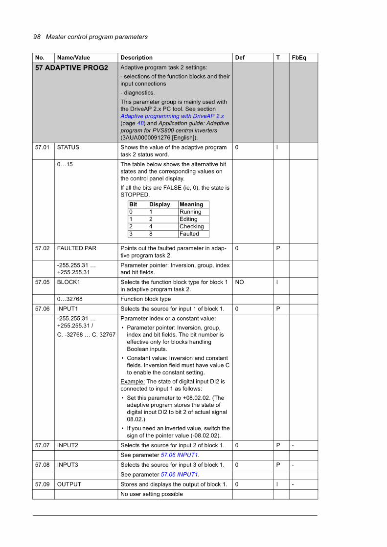
98 Master control program parameters
57 ADAPTIVE PROG2 Adaptive program task 2 settings:
- selections of the function blocks and their input connections
- diagnostics.
This parameter group is mainly used with the DriveAP 2.x PC tool. See section Adaptive programming with DriveAP 2.x (page 48) and Application guide: Adaptive program for PVS800 central inverters (3AUA0000091276 [English]).
57.01 STATUS Shows the value of the adaptive program task 2 status word.
0 I
0…15 The table below shows the alternative bit states and the corresponding values on the control panel display.
If all the bits are FALSE (ie, 0), the state is STOPPED.
57.02 FAULTED PAR Points out the faulted parameter in adap-tive program task 2.
0 P
-255.255.31 … +255.255.31
Parameter pointer: Inversion, group, index and bit fields.
57.05 BLOCK1 Selects the function block type for block 1 in adaptive program task 2.
NO I
0…32768 Function block type
57.06 INPUT1 Selects the source for input 1 of block 1. 0 P
-255.255.31 … +255.255.31 /
C. -32768 … C. 32767
Parameter index or a constant value:
• Parameter pointer: Inversion, group, index and bit fields. The bit number is effective only for blocks handling Boolean inputs.
• Constant value: Inversion and constant fields. Inversion field must have value C to enable the constant setting.
Example: The state of digital input DI2 is connected to input 1 as follows:
• Set this parameter to +08.02.02. (The adaptive program stores the state of digital input DI2 to bit 2 of actual signal 08.02.)
• If you need an inverted value, switch the sign of the pointer value (-08.02.02).
57.07 INPUT2 Selects the source for input 2 of block 1. 0 P -
See parameter 57.06 INPUT1.
57.08 INPUT3 Selects the source for input 3 of block 1. 0 P -
See parameter 57.06 INPUT1.
57.09 OUTPUT Stores and displays the output of block 1. 0 I -
No user setting possible
No. Name/Value Description Def T FbEq
Bit Display Meaning0 1 Running1 2 Editing2 4 Checking3 8 Faulted

Master control program parameters 99
57.10 BLOCK2 Selects the function block type for block 2 in adaptive program task 2.
NO I -
0…32768 Function block type
57.11 INPUT1 Selects the source for input 1 of block 2. 0 P -
See parameter 57.06 INPUT1.
57.12 INPUT2 Selects the source for input 2 of block 2. 0 P -
See parameter 57.06 INPUT1.
57.13 INPUT Selects the source for input 3 of block 2. 0 P -
See parameter 57.06 INPUT1.
57.14 OUTPUT Stores and displays the output of block 2. 0 I -
No user setting possible
57.15 BLOCK3 Selects the function block type for block 3 in adaptive program task 2.
NO I -
0…32768 Function block type
… … … … … …
57.104 OUTPUT Stores and displays the output of block 20. I -
0…32768 No user setting possible 0
58 ADAPT PROG2 CTRL
Adaptive program task 2 control. Update time of task 2 control is 100 ms. This parameter group is mainly used with the DriveAP 2.x PC tool.
See parameter group 57 ADAPTIVE PROG2.
58.01 ADAPT PROG CMD Selects the operation mode for adaptive program task 2.
EDIT I
STOP Stopped. Program cannot be edited. 1
START Running. Program cannot be edited. 2
EDIT Stops to edit the mode. Program can be edited.
3
58.02 EDIT CMD Selects the command for the block placed in the location defined by parameter 58.03 EDIT BLOCK. Program must be in the edit-ing mode (see parameter 58.01 ADAPT PROG CMD).
NO I
NO Home value. Value automatically reverts to NO after an editing command is executed.
1
PUSH Shifts the block in the location defined by parameter 58.03 EDIT BLOCK and the subsequent blocks one location up. New block can be placed in the emptied loca-tion.
2
DELETE Selects the block in the location defined by parameter 58.03 EDIT BLOCK and shifts the subsequent blocks one step down.
3
No. Name/Value Description Def T FbEq

100 Master control program parameters
PROTECT Activation of the task protection: Read-pro-tects the input connections of the blocks. Activate as follows:
- Ensure the task operation mode is set to START or STOP (parameter 58.01 ADAPT PROG CMD).
- Set the passcode by parameter 58.05 PASSCODE.
- Set parameter 58.02 to PROTECT.
When protection is activated:
- All parameters in group 57 ADAPTIVE PROG2 excluding the block output param-eters are hidden (read-protected).
- It is not possible to switch the task operat-ing mode (parameter 58.01 ADAPT PROG CMD) to the editing mode.
- Parameter 58.05 PASSCODE value is set to 0.
4
UNPROTECT Deactivation of the task protection: no read protection of the input connection of the blocks. Deactivate as follows:
- Ensure the adaptive task operation mode is set to START or STOP (parameter 58.01 ADAPT PROG CMD).
- Set the passcode by parameter 58.05 PASSCODE.
- Set parameter 58.02 to UNPROTECT.
5
58.03 EDIT BLOCK Defines the block location number for the command selected by parameter 58.02 EDIT CMD.
0 I -
1…15 Block location number
58.04 TIMELEV_SEL Indicates the fixed execution cycle time of 100 ms for adaptive program task 2.
100ms I -
58.05 PASSCODE Defines the passcode, which acti-vates/deactivates the protection of the input connections of the blocks. See parameter 58.02 EDIT CMD.
0 I -
0 h…FFFFFF h Passcode. The setting restores to 0 after the protection is activated/deactivated.
Note: When you activate the protection, write down the passcode and store it for later use.
No. Name/Value Description Def T FbEq

Master control program parameters 101
65 FUNC GENERATOR Defines a five-point [(x1, y1), (x2, y2), (x3, y3), (x4, y4), (x5, y5)] function curve in the adaptive program. See blocks FUNG IN and FUNG OUT in Application guide: Adaptive program for PVS800 central inverters (3AUA0000091276 [English]).
Function is executed on 100 ms time level. Function generator can be used, eg, for defining pump acceleration curves.
65.01 ENABLE Activates the function. OFF B
OFF Inactive 0
ON Active 65535
65.03 OUT Defines the output of the function curve. 0 R
-32768…32767 Value 1 = 1
65.04 X1 Defines the value for the x-axis 1st point (x1, y1).
0 R
-32768…32767 Value 1 = 1
65.05 Y1 Defines the value for the y-axis 1st point (x1, y1).
0 R
-32768…32767 Value 1 = 1
65.06 X2 Defines the value for the x-axis 2nd point (x2, y2).
0 R
-32768…32767 Value 1 = 1
65.07 Y2 Defines the value for the y-axis 2nd point (x2, y2).
0 R
-32768…32767 Value 1 = 1
65.08 X3 Defines the value for the x-axis 3rd point (x3, y3).
0 R
-32768…32767 Value 1 = 1
65.09 Y3 Defines the value for the y-axis 3rd point (x3, y3).
0 R
-32768…32767 Value 1 = 1
65.10 X4 Defines the value for the x-axis 4th point (x4, y4).
0 R
-32768…32767 Value 1 = 1
65.11 Y4 Defines the value for the y-axis 4th point (x4, y4).
0 R
-32768…32767 Value 1 = 1
65.12 X5 Defines the value for the x-axis 5th point (x5, y5).
0 R
-32768…32767 Value 1 = 1
65.13 Y5 Defines the value for the y-axis 5th point (x5, y5).
0 R
-32768…32767 Value 1 = 1
No. Name/Value Description Def T FbEq
X1 X5…
Y1
Y5
…

102 Master control program parameters
66 ADAPTIVE CONNECT
This group consists of input type parame-ters for the adaptive program. Note: It is recommended that these parameter val-ues be set with the DriveAP 2.x PC tool.
See section Adaptive programming with DriveAP 2.x (page 48) and Application guide: Adaptive program for PVS800 cen-tral inverters (3AUA0000091276 [English]).
66.01 CW Defines the input for block CW.
See also parameter 07.02 USED MCW.
0 P
-255.255.31 … +255.255.31 /
C. -32768 …C. 32767
Parameter pointer or a constant value:
• Parameter pointer: Inversion, group, index and bit fields. Bit number is effective only for blocks handling Boolean inputs.
• Constant value: Inversion and constant fields. Inversion field must have value C to enable the constant setting.
1 = 1
66.02 DO1 Defines the input for block DO1 which con-trols relay output RO1 on the control unit.
0 P
Signal index or constant value, see param-eter 66.01 CW.
1 = 1
66.03 DO2 Defines the input for block DO2 which con-trols relay output RO2 on the control unit.
-.008.001.03 P
Signal index or constant value, see param-eter 66.01 CW.
1 = 1
66.04 DO3 Defines the input for block DO3 which con-trols relay output RO3 on the control unit.
+.136.020.00 P
Signal index or constant value, see param-eter 66.01 CW.
1 = 1
No. Name/Value Description Def T FbEq
Bit Name Value Description0 ON/OFF 0 1 Inverter operation is enabled. Bit 0 and bit 3 must be con-
trolled at the same time.0 Operation is disabled.
1, 2 Reserved3 ON/OFF 1 Operation is enabled.
0 Operation is disabled.4…6 Reserved7 RESET 0 1 Reset8…15 Reserved

Master control program parameters 103
66.05 EXT DO Defines the input for block EXT DO which controls extension module digital outputs (EXT DO word). Updating interval is 100 ms.
0 P
Signal index or constant value, see param-eter 66.01 CW.
1 = 1
66.06 AO1 Defines the input for block AO1 which con-trols analog output 1 on the control unit.
0 P
Signal index or constant value, see param-eter 66.01 CW.
1 = 1
66.07 AO2 Defines the input for block AO2 which con-trols analog output 2 on the control unit.
0 P
Signal index or constant value, see param-eter 66.01 CW.
1 = 1
66.08 EXT1 AO1 Defines the input for block EXT1 AO1 which controls analog output 1 of exten-sion module 1.
0 P
Signal index or constant value, see param-eter 66.01 CW.
1 = 1
66.09 EXT1 AO2 Defines the input for block EXT1 AO2 which controls analog output 2 of exten-sion module 1.
0 P
Signal index or constant value, see param-eter 66.01 CW.
1 = 1
66.10 EXT2 AO1 Defines the input for block EXT2 AO1 which controls analog output 1 of exten-sion module 2.
0 P
Signal index or constant value, see param-eter 66.01 CW.
1 = 1
66.11 EXT2 AO2 Defines the input for block EXT2 AO2 which controls analog output 2 of exten-sion module 2.
0 P
Signal index or constant value, see param-eter 66.01 CW.
1 = 1
66.12 EXT3 AO1 Defines the input for block EXT3 AO1 which controls analog output 1 of exten-sion module 3.
0 P
Signal index or constant value, see param-eter 66.01 CW.
1 = 1
No. Name/Value Description Def T FbEq
Bit Name Description0 EXT1 DO1 Digital output 1 control on RDIO extension module 11 EXT1 DO2 Digital output 2 control on RDIO extension module 12 EXT2 DO1 Digital output 1 control on RDIO extension module 23 EXT2 DO2 Digital output 2 control on RDIO extension module 24 EXT3 DO1 Digital output 1 control on RDIO extension module 35 EXT3 DO2 Digital output 2 control on RDIO extension module 36 EXT4 DO1 Digital output 1 control on RDIO extension module 47 EXT4 DO2 Digital output 2 control on RDIO extension module 48 EXT5 DO1 Digital output 1 control on RDIO extension module 59 EXT5 DO2 Digital output 2 control on RDIO extension module 510…15 Reserved

104 Master control program parameters
66.13 EXT3 AO2 Defines the input for block EXT3 AO2 which controls analog output 2 of exten-sion module 3.
0 P
Signal index or constant value, see param-eter 66.01 CW.
1 = 1
66.14 EXT4 AO1 Defines the input for block EXT4 AO1 which controls analog output 1 of exten-sion module 4.
0 P
Signal index or constant value, see param-eter 66.01 CW.
1 = 1
66.15 EXT4 AO2 Defines the input for block EXT4 AO2 which controls analog output 2 of exten-sion module 4.
0 P
Signal index or constant value, see param-eter 66.01 CW.
1 = 1
66.16 EXT5 AO1 Defines the input for block EXT5 AO1 which controls analog output 1 of exten-sion module 5.
0 P
Signal index or constant value, see param-eter 66.01 CW.
1 = 1
66.17 EXT5 AO2 Defines the input for block EXT5 AO2 which controls analog output 2 of exten-sion module 5.
0 P
Signal index or constant value, see param-eter 66.01 CW.
1 = 1
66.18 FUNC GEN Defines an input for function generator input. This signal is mainly used with DriveAP PC tool.
0 P
C -32768 …C 32767 Constant value 1 = 1
66.19 AP AFW Defines an alarm and fault word for the adaptive program.
0 P
Signal index or constant value, see param-eter 66.01 CW.
1 = 1
66.20 EXT6 AO1 Defines the input for block EXT6 AO1 which controls analog output 1 of exten-sion module 6.
0 P
Signal index or constant value, see param-eter 66.01 CW.
1 = 1
66.21 EXT6 AO2 Defines the input for block EXT6 AO2 which controls analog output 2 of exten-sion module 6.
0 P
Signal index or constant value, see param-eter 66.01 CW.
1 = 1
66.22 EXT7 AO1 Defines the input for block EXT7 AO1 which controls analog output 1 of exten-sion module 7.
0 P
Signal index or constant value, see param-eter 66.01 CW.
1 = 1
66.23 EXT7 AO2 Defines the input for block EXT7 AO2 which controls analog output 2 of exten-sion module 7.
0 P
Signal index or constant value, see param-eter 66.01 CW.
1 = 1
No. Name/Value Description Def T FbEq
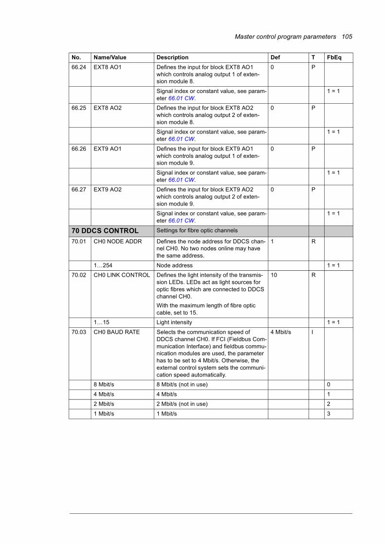
Master control program parameters 105
66.24 EXT8 AO1 Defines the input for block EXT8 AO1 which controls analog output 1 of exten-sion module 8.
0 P
Signal index or constant value, see param-eter 66.01 CW.
1 = 1
66.25 EXT8 AO2 Defines the input for block EXT8 AO2 which controls analog output 2 of exten-sion module 8.
0 P
Signal index or constant value, see param-eter 66.01 CW.
1 = 1
66.26 EXT9 AO1 Defines the input for block EXT9 AO1 which controls analog output 1 of exten-sion module 9.
0 P
Signal index or constant value, see param-eter 66.01 CW.
1 = 1
66.27 EXT9 AO2 Defines the input for block EXT9 AO2 which controls analog output 2 of exten-sion module 9.
0 P
Signal index or constant value, see param-eter 66.01 CW.
1 = 1
70 DDCS CONTROL Settings for fibre optic channels
70.01 CH0 NODE ADDR Defines the node address for DDCS chan-nel CH0. No two nodes online may have the same address.
1 R
1…254 Node address 1 = 1
70.02 CH0 LINK CONTROL Defines the light intensity of the transmis-sion LEDs. LEDs act as light sources for optic fibres which are connected to DDCS channel CH0.
With the maximum length of fibre optic cable, set to 15.
10 R
1…15 Light intensity 1 = 1
70.03 CH0 BAUD RATE Selects the communication speed of DDCS channel CH0. If FCI (Fieldbus Com-munication Interface) and fieldbus commu-nication modules are used, the parameter has to be set to 4 Mbit/s. Otherwise, the external control system sets the communi-cation speed automatically.
4 Mbit/s I
8 Mbit/s 8 Mbit/s (not in use) 0
4 Mbit/s 4 Mbit/s 1
2 Mbit/s 2 Mbit/s (not in use) 2
1 Mbit/s 1 Mbit/s 3
No. Name/Value Description Def T FbEq

106 Master control program parameters
70.04 CH0 TIMEOUT Defines the time delay before channel CH0 or type Rxxx fieldbus adapter interface communication break alarm/fault (COMM MODULE) is activated. Time count starts when the link fails to update the communi-cation message. Action taken by the PVS800 on a communication break is defined by parameter 70.05 CH0 COM LOSS CTRL.
When the parameter is set to zero, time is not monitored and COMM MODULE fault is not indicated regardless of the value of parameter 70.05 CH0 COM LOSS CTRL.
100 ms R
0…60000 ms Time 1 = 1 ms
70.05 CH0 COM LOSS CTRL
Selects how the PVS800 reacts when communication error on DDCS channel CH0 or on type Rxxx fieldbus adapter interface is detected. Time delay for the communication break alarm/fault activation is defined by parameter 70.04 CH0 TIME-OUT.
Note: This parameter is in use when exter-nal serial communication is activated by parameter 98.02 COMM. MODULE.
FAULT I
NO FAULT PVS800 generates warning COMM MOD-ULE.
1
FAULT PVS800 trips on fault COMM MODULE. 2
70.06 CH1 LINK CONTROL Defines the light intensity of the transmis-sion LEDs. LEDs act as light sources for optic fibres which are connected to DDCS channel CH1.
With the maximum length of fibre optic cable, use value 15.
10 R
1…15 Light intensity 1 = 1
70.13 CH2 TIMEOUT Defines the communication time-out for channel CH2 in milliseconds.
100 ms I
0…10000 Time-out in milliseconds, 0 = not in use 1 = 1 ms
70.15 CH3 NODE ADDR Defines the node address for DDCS chan-nel CH3. No two nodes online may have the same address. Typically the setting needs to be changed when the master control unit is connected in a ring configu-ration which consists of several inverters and a PC with a DriveWindow PC tool.
Note: The new node address becomes valid only after the next power-up of the control unit.
1 R
1…254 Node address 1 = 1
70.16 CH3 LINK CONTROL Defines the light intensity of the transmis-sion LEDs. LEDs act as light sources for optic fibres which are connected to DDCS channel CH3.
With the maximum length of fibre optic cable, use value 15.
15 R
1…15 Light intensity 1 = 1
No. Name/Value Description Def T FbEq

Master control program parameters 107
70.19 CH0 HW CONNECTION
Selects the topology of the DDCS channel CH0 link.
Note: This parameter is not in use in the DriveBus mode.
RING B
RING Devices are connected in a ring. 0
STAR Devices are connected in a star. 65535
70.20 CH3 HW CONNECTION
Selects the topology of the DDCS channel CH3 link.
RING B
RING Control units are connected in a ring. 0
STAR Control units are connected in a star. 65535
70.32 CH2 HW CONNECTION
Selects the topology of the DDCS channel CH2 link.
STAR B
RING Devices are connected in a ring. 0
STAR Devices are connected in a star. 65535
71 DRIVEBUS COMM Channel CH0 DriveBus settings
71.01 CH0 DRIVEBUS MODE
Selects the communication mode for the DDCS channel CH0. New mode becomes valid only after the next power-up of the PVS800. Data is exchanged 4 times faster in the DriveBus mode than in the DDCS mode. Use the same value as the overrid-ing control device.
NO B
NO DDCS mode 0
YES DriveBus mode 65535
81 CH2 RECEIVE ADDR Addresses where the master control pro-gram writes data words from DDCS CH2
81.01 CH2 DS27 VAL 1 Defines an address where data word 1 of dataset 27 is written.
104 I
0…20000 Update time is 500 ms. 1 = 1
81.02 CH2 DS27 VAL 2 Defines an address where data word 2 of dataset 27 is written.
105 I
0…20000 Update time is 500 ms. 1 = 1
81.03 CH2 DS27 VAL 3 Defines an address where data word 3 of dataset 27 is written.
106 I
0…20000 Update time is 500 ms. 1 = 1
81.04 CH2 DS29 VAL 1 Defines an address where data word 1 of dataset 29 is written.
113 I
0…20000 Update time is 500 ms. 1 = 1
81.05 CH2 DS29 VAL 2 Defines an address where data word 2 of dataset 29 is written.
808 I
0…20000 Update time is 500 ms. 1 = 1
81.06 CH2 DS29 VAL 3 Defines an address where data word 3 of dataset 29 is written.
203 I
0…20000 Update time is 500 ms. 1 = 1
81.07 CH2 DS31 VAL 1 Defines an address where data word 1 of dataset 31 is written.
108 I
0…20000 Update time is 500 ms. 1 = 1
81.08 CH2 DS31 VAL 2 Defines an address where data word 2 of dataset 31 is written.
109 I
0…20000 Update time is 500 ms. 1 = 1
No. Name/Value Description Def T FbEq
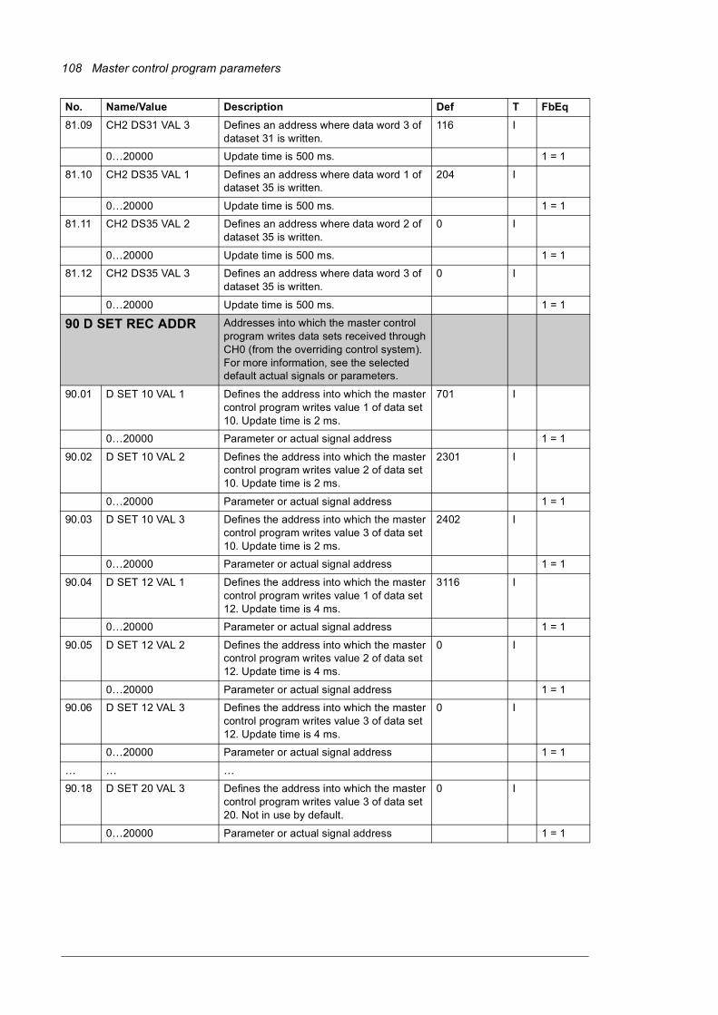
108 Master control program parameters
81.09 CH2 DS31 VAL 3 Defines an address where data word 3 of dataset 31 is written.
116 I
0…20000 Update time is 500 ms. 1 = 1
81.10 CH2 DS35 VAL 1 Defines an address where data word 1 of dataset 35 is written.
204 I
0…20000 Update time is 500 ms. 1 = 1
81.11 CH2 DS35 VAL 2 Defines an address where data word 2 of dataset 35 is written.
0 I
0…20000 Update time is 500 ms. 1 = 1
81.12 CH2 DS35 VAL 3 Defines an address where data word 3 of dataset 35 is written.
0 I
0…20000 Update time is 500 ms. 1 = 1
90 D SET REC ADDR Addresses into which the master control program writes data sets received through CH0 (from the overriding control system). For more information, see the selected default actual signals or parameters.
90.01 D SET 10 VAL 1 Defines the address into which the master control program writes value 1 of data set 10. Update time is 2 ms.
701 I
0…20000 Parameter or actual signal address 1 = 1
90.02 D SET 10 VAL 2 Defines the address into which the master control program writes value 2 of data set 10. Update time is 2 ms.
2301 I
0…20000 Parameter or actual signal address 1 = 1
90.03 D SET 10 VAL 3 Defines the address into which the master control program writes value 3 of data set 10. Update time is 2 ms.
2402 I
0…20000 Parameter or actual signal address 1 = 1
90.04 D SET 12 VAL 1 Defines the address into which the master control program writes value 1 of data set 12. Update time is 4 ms.
3116 I
0…20000 Parameter or actual signal address 1 = 1
90.05 D SET 12 VAL 2 Defines the address into which the master control program writes value 2 of data set 12. Update time is 4 ms.
0 I
0…20000 Parameter or actual signal address 1 = 1
90.06 D SET 12 VAL 3 Defines the address into which the master control program writes value 3 of data set 12. Update time is 4 ms.
0 I
0…20000 Parameter or actual signal address 1 = 1
… … …
90.18 D SET 20 VAL 3 Defines the address into which the master control program writes value 3 of data set 20. Not in use by default.
0 I
0…20000 Parameter or actual signal address 1 = 1
No. Name/Value Description Def T FbEq

Master control program parameters 109
91 D SET REC ADDR Addresses into which the master control program writes data sets received through CH0 (from the overriding control system)
91.01 D SET 22 VAL 1 Defines the address into which the master control program writes value 1 of data set 22. Not in use by default.
0 I
0…20000 Parameter or actual signal address 1 = 1
… … …
91.06 D SET 24 VAL 3 Defines the address into which the master control program writes value 3 of data set 24. Not in use by default.
0 I
0…20000 Parameter or actual signal address 1 = 1
92 D SET TR ADDR Addresses from which the master control program reads data sets to be sent through CH0 (to the overriding control sys-tem)
92.01 D SET 11 VAL 1 Defines the address from which the master control program reads value 1 of data set 11. Update time is 2 ms.
801 I
0…20000 Parameter or actual signal address 1 = 1
92.02 D SET 11 VAL 2 Defines the address from which the master control program reads value 2 of data set 11. Update time is 2 ms.
110 I
0…20000 Parameter or actual signal address 1 = 1
92.03 D SET 11 VAL 3 Defines the address from which the master control program reads value 3 of data set 11. Update time is 2 ms.
107 I
0…20000 Parameter or actual signal address 1 = 1
92.04 D SET 13 VAL 1 Defines the address from which the master control program reads value 1 of data set 13. Update time is 4 ms.
0 I
0…20000 Parameter or actual signal address 1 = 1
92.05 D SET 13 VAL 2 Defines the address from which the master control program reads value 2 of data set 13. Update time is 4 ms.
0 I
0…20000 Parameter or actual signal address 1 = 1
92.06 D SET 13 VAL 3 Defines the address from which the master control program reads value 3 of data set 13. Update time is 4 ms.
0 I
0…20000 Parameter or actual signal address 1 = 1
92.07 D SET 15 VAL 1 Defines the address from which the master control program reads value 1 of data set 15. Update time is 10 ms. Not in use by default.
0 I
0…20000 Parameter or actual signal address 1 = 1
92.08 D SET 15 VAL 2 Defines the address from which the master control program reads value 2 of data set 15. Update time is 10 ms. Not in use by default.
0 I
0…20000 Parameter or actual signal address 1 = 1
No. Name/Value Description Def T FbEq

110 Master control program parameters
92.09 D SET 15 VAL 3 Defines the address from which the master control program reads value 3 of data set 15. Update time is 10 ms. Not in use by default.
0 I
0…20000 Parameter or actual signal address 1 = 1
92.10 D SET 17 VAL 1 Defines the address from which the master control program reads value 1 of data set 17. Update time is 10 ms.
0 I
0…20000 Parameter or actual signal address 1 = 1
92.11 D SET 17 VAL 2 Defines the address from which the master control program reads value 2 of data set 17. Update time is 10 ms.
0 I
0…20000 Parameter or actual signal address 1 = 1
92.12 D SET 17 VAL 3 Defines the address from which the master control program reads value 3 of data set 17. Update time is 10 ms.
0 I
0…20000 Parameter or actual signal address 1 = 1
… … …
92.18 D SET 21 VAL 3 Defines the address from which the master control program reads value 3 of data set 21. Not in use by default.
0 I
0…20000 Parameter or actual signal address 1 = 1
93 D SET TR ADDR Addresses from which the master control program reads data sets to be sent through CH0 (to the overriding control sys-tem)
93.01 D SET 23 VAL 1 Defines the address from which the master control program reads value 1 of data set 23. Not in use by default.
0 0
0…20000 Parameter or actual signal address 1 = 1
… … …
93.06 D SET 25 VAL 3 Defines the address from which the master control program reads value 3 of data set 25. Not in use by default.
0 0
0…20000 Parameter or actual signal address 1 = 1
98 OPTION MODULES Activation of optional modules and external serial communication.
R-type fieldbus adapter modules are con-nected to Slot 1 or 2 of the control unit or via the optional AIMA-01 I/O Module Adapter connected to control unit DDCS channel CH1. Multiple AIMA-01 adapters are connected in a ring.
N-type fieldbus adapter modules are con-nected to control unit DDCS channel CH0.
98.02 COMM. MODULE Selects an interface for the external control location.
NO I
NO Inverter communicates with direct parameter read/write commands without timeout monitoring. External dataset interface is not used, i.e. parameter values cannot be read or written through datasets.
1
No. Name/Value Description Def T FbEq

Master control program parameters 111
FIELDBUS Activates dataset communication through datasets 1 and 2.
With this selection the inverter expects cyclical data writing to dataset 1 (Modbus addresses 1...3) through RETA-01, RETA-02, or NETA-21. Timeout monitoring can be disabled by setting a value of 0 to parameter 70.04 CH0 TIMEOUT. See also parameter group 70 DDCS CONTROL and chapter Fieldbus control (page 197).
2
ADVANT/N-FB Activates external dataset communication through datasets 10...25.
With this selection the inverter expects cyclical data writing to dataset 10 (Modbus addresses 28..30) through RETA-01, RETA-02, or NETA-21. Timeout monitoring can be disabled by setting a value of 0 to parameter 70.04 CH0 TIMEOUT.See also parameter group 70 DDCS CON-TROL and chapter Fieldbus control (page 197).
3
STD MODBUS Activates external dataset communication through datasets 1 and 2.
With this selection the inverter expects cyclical data writing to dataset 1 (Modbus addresses 1..3) through RMBA-01 Modbus adapter module.
See Modbus parameter settings in group 52 STANDARD MODBUS.
4
98.04 DI/O EXT1 LOC Activates the communication to the optional digital I/O extension module 1 and defines the type and connection interface of the module.
Faster DC input signal detection can be achieved by disabling the hardware filter of the digital input with the configuration DIP switch on the circuit board of the module.
Note: Always enable the hardware filtering with an AC input signal.
NOT IN USE I
NOT IN USE Inactive 2
RDIO-SLOT1 Communication active. Module type: RDIO. Connection interface: option slot 1 of the control unit.
3
RDIO-SLOT2 Communication active. Module type: RDIO. Connection interface: option slot 2 of the control unit.
4
No. Name/Value Description Def T FbEq
ON
1 2 3 4
EnabledDisabled
DI1DI2DI3
Hardware
DIP switch S2 (RDIO)
filtering

112 Master control program parameters
RDIO-DDCS Communication active. Module type: RDIO. Connection interface: Optional I/O module adapter (AIMA) that communicates with the control unit through a fibre optic DDCS link.
Note: The module node number must be set to 5 with switch S1.
5
98.05 DI/O EXT2 LOC See parameter 98.04 DI/O EXT1 LOC.
NOT IN USE I
98.06 DI/O EXT3 LOC See parameter 98.04 DI/O EXT1 LOC.
NOT IN USE I
98.07 DI/O EXT4 LOC See parameter 98.04 DI/O EXT1 LOC.
NOT IN USE I
98.08 DI/O EXT5 LOC See parameter 98.04 DI/O EXT1 LOC.
NOT IN USE I
98.09 AI/O EXT1 LOC Activates the communication to the optional analog I/O extension module 1, and defines the type and connection inter-face of the module.
NOT IN USE I
NOT IN USE Communication inactive 2
RAIO-SLOT1 Communication active. Module type: RAIO. Connection interface: option slot 1 of the control unit.
3
RAIO-SLOT2 Communication active. Module type: RAIO. Connection interface: option slot 2 of the control unit.
4
RAIO-DDCS Communication active. Module type: RAIO. Connection interface: Optional I/O module adapter (AIMA) that communicates with the control unit through a fibre optic DDCS link.
Note: The module node number must be set to A with switch S1.
5
No. Name/Value Description Def T FbEq
Switch S1
AB
CD E F 0
12
345678
9
5
Switch S1
AB
C D E F 01
2
345678
9
6
Switch S1
AB
C D E F 01
2
345678
9
7
Switch S1
AB
C D E F 01
2
345678
9
8
Switch S1
AB
C D E F 01
2
345678
9
9
Switch S1
AB
CD E F 0
12
345678
9
A

Master control program parameters 113
98.10 AI/O EXT2 LOC See parameter 98.09 AI/O EXT1 LOC.
Note: The RAIO-01 modules with parame-ter selection RAIO-SLOT1 and RAIO-SLOT2. can be used as analogue outputs only. The inputs are disabled.
NOT IN USE I
98.11 AI/O EXT3 LOC See parameter 98.09 AI/O EXT1 LOC.
See also note in 98.10 AI/O EXT2 LOC.
NOT IN USE I
98.12 AI/O EXT4 LOC See parameter 98.09 AI/O EXT1 LOC.
See also note in 98.10 AI/O EXT2 LOC.
NOT IN USE I
98.13 AI/O EXT5 LOC See parameter 98.09 AI/O EXT1 LOC.
See also note in 98.10 AI/O EXT2 LOC.
NOT IN USE I
98.14 AI/O EXT6 LOC See parameter 98.09 AI/O EXT1 LOC.
See also note in 98.10 AI/O EXT2 LOC.
NOT IN USE I
98.15 AI/O EXT7 LOC See parameter 98.09 AI/O EXT1 LOC.
See also note in 98.10 AI/O EXT2 LOC.
NOT IN USE I
98.16 AI/O EXT8LOC See parameter 98.09 AI/O EXT1 LOC.
See also note in 98.10 AI/O EXT2 LOC.
NOT IN USE I
98.17 AI/O EXT9 LOC See parameter 98.09 AI/O EXT1 LOC.
See also note in 98.10 AI/O EXT2 LOC.
NOT IN USE I
99 START-UP DATA Language, application macro selection, etc.
99.01 LANGUAGE Selects the display language. ENGLISH I
No. Name/Value Description Def T FbEq
Switch S1
AB
CD E F 0
12
345678
9
B
Switch S1
AB
C D E F 01
2
345678
9
C
Switch S1
AB
C D E F 01
2
345678
9
D
Switch S1
AB
C D E F 01
2
345678
9E
Switch S1
AB
C D E F 01
2
345678
9
1
Switch S1
AB
C D E F 01
2
345678
9
2
Switch S1
AB
C D E F 01
2
345678
9
3
Switch S1
AB
C D E F 01
2
345678
9
4

114 Master control program parameters
99.02 APPLIC SELECTOR Selects the application. PHOTO-VOLTAIC
I
PHOTOVOLTAIC Solar inverter 1
99.09 APPLIC RESTORE Restores the original parameter settings. 0 I
NO No 0
YES Yes 1
No. Name/Value Description Def T FbEq

Inverter control program parameters 115
6
Inverter control program parameters
What this chapter containsThis chapter describes the inverter control program parameters of the PVS800. All connections discussed in the parameter descriptions of this chapter refer to those of the inverter control unit (RDCU unit, designation A41) unless otherwise indicated. This control unit is shown as “PVS800 xxxx_5PV” (“xxxx” depending on power rating), and has the ID number 2. The control program revision is of the format ISXR7xxx.
Parameter groups 10…99 are usually user-adjustable. Parameter groups 1…9 (actual signals) are only for monitoring and read-only, though data can be written into the Control Words (parameter group 7) through an external control system.
WARNING! The PVS800 is intended to be configurable through the parameters of the master control program (see page 49). Some parameters in the inverter control program may be accessed but are not listed in this manual at all; do not adjust
these parameters without consulting with ABB as incorrect parameter values may cause malfunctioning or even damage to the equipment.
Note:
• Many parameters of the inverter control program are available through the master control program (see page 49). In these cases, the description is provided at the master control program parameter; the Description field in the following table only includes a reference to the corresponding master control program (MCP) parameter and page number, for example “MCP 01.06 LINE CURRENT (51)”.
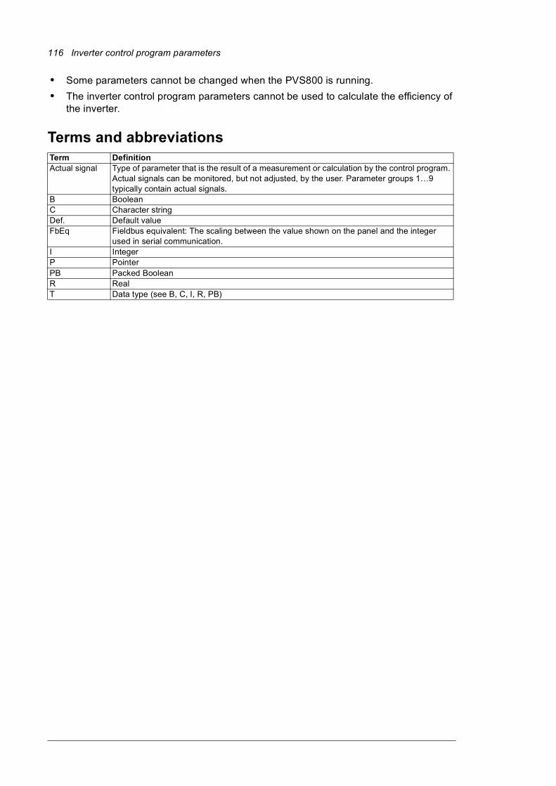
116 Inverter control program parameters
• Some parameters cannot be changed when the PVS800 is running.
• The inverter control program parameters cannot be used to calculate the efficiency of the inverter.
Terms and abbreviationsTerm DefinitionActual signal Type of parameter that is the result of a measurement or calculation by the control program.
Actual signals can be monitored, but not adjusted, by the user. Parameter groups 1…9 typically contain actual signals.
B BooleanC Character stringDef. Default valueFbEq Fieldbus equivalent: The scaling between the value shown on the panel and the integer
used in serial communication.I IntegerP PointerPB Packed BooleanR RealT Data type (see B, C, I, R, PB)
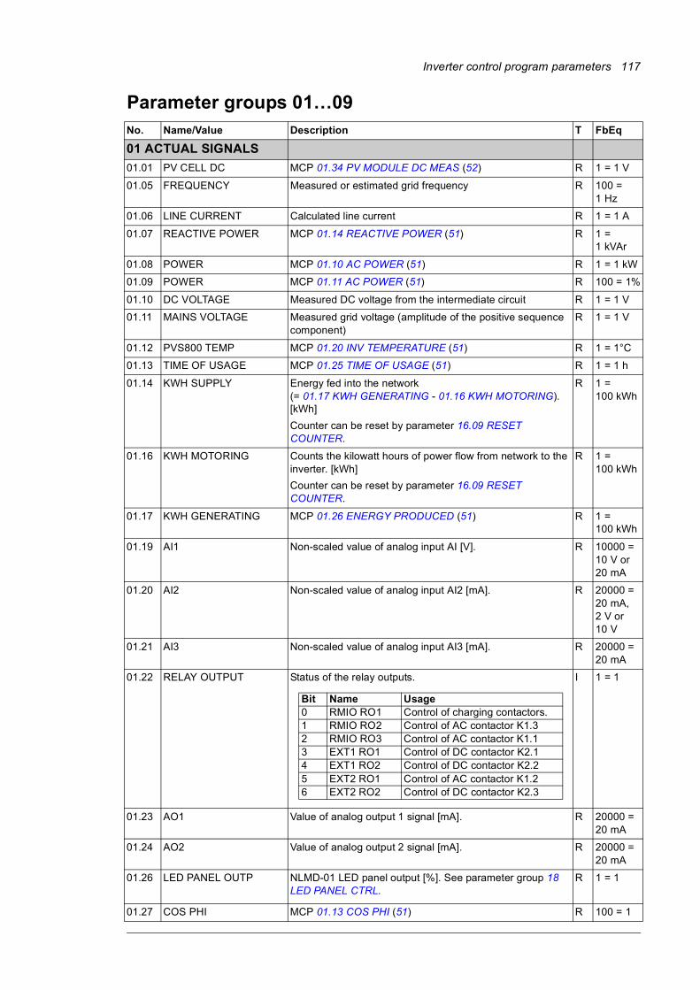
Inverter control program parameters 117
Parameter groups 01…09No. Name/Value Description T FbEq
01 ACTUAL SIGNALS
01.01 PV CELL DC MCP 01.34 PV MODULE DC MEAS (52) R 1 = 1 V
01.05 FREQUENCY Measured or estimated grid frequency R 100 = 1 Hz
01.06 LINE CURRENT Calculated line current R 1 = 1 A
01.07 REACTIVE POWER MCP 01.14 REACTIVE POWER (51) R 1 = 1 kVAr
01.08 POWER MCP 01.10 AC POWER (51) R 1 = 1 kW
01.09 POWER MCP 01.11 AC POWER (51) R 100 = 1%
01.10 DC VOLTAGE Measured DC voltage from the intermediate circuit R 1 = 1 V
01.11 MAINS VOLTAGE Measured grid voltage (amplitude of the positive sequence component)
R 1 = 1 V
01.12 PVS800 TEMP MCP 01.20 INV TEMPERATURE (51) R 1 = 1°C
01.13 TIME OF USAGE MCP 01.25 TIME OF USAGE (51) R 1 = 1 h
01.14 KWH SUPPLY Energy fed into the network (= 01.17 KWH GENERATING - 01.16 KWH MOTORING). [kWh]
Counter can be reset by parameter 16.09 RESET COUNTER.
R 1 = 100 kWh
01.16 KWH MOTORING Counts the kilowatt hours of power flow from network to the inverter. [kWh]
Counter can be reset by parameter 16.09 RESET COUNTER.
R 1 = 100 kWh
01.17 KWH GENERATING MCP 01.26 ENERGY PRODUCED (51) R 1 = 100 kWh
01.19 AI1 Non-scaled value of analog input AI [V]. R 10000 = 10 V or 20 mA
01.20 AI2 Non-scaled value of analog input AI2 [mA]. R 20000 = 20 mA, 2 V or 10 V
01.21 AI3 Non-scaled value of analog input AI3 [mA]. R 20000 = 20 mA
01.22 RELAY OUTPUT Status of the relay outputs. I 1 = 1
01.23 AO1 Value of analog output 1 signal [mA]. R 20000 = 20 mA
01.24 AO2 Value of analog output 2 signal [mA]. R 20000 = 20 mA
01.26 LED PANEL OUTP NLMD-01 LED panel output [%]. See parameter group 18 LED PANEL CTRL.
R 1 = 1
01.27 COS PHI MCP 01.13 COS PHI (51) R 100 = 1
Bit Name Usage0 RMIO RO1 Control of charging contactors.1 RMIO RO2 Control of AC contactor K1.32 RMIO RO3 Control of AC contactor K1.13 EXT1 RO1 Control of DC contactor K2.14 EXT1 RO2 Control of DC contactor K2.25 EXT2 RO1 Control of AC contactor K1.26 EXT2 RO2 Control of DC contactor K2.3

118 Inverter control program parameters
01.28 P LIMITED Maximum instantaneous active power which the inverter can feed to the grid.
R 1 = 1 kW
01.29 INSUL RESISTANCE Measured insulation resistance from the solar generator. This signal is valid only if the inverter is equipped with option +Q954. See parameter 16.18 INSUL MEAS SELECT.
R 1 = 1 kOhm
01.30 BREAKER COUNTER MCP 01.30 BREAKER COUNTER (52) R 1 = 1
01.31 FAN ON-TIME Running time of the inverter cooling fan [h]
Counter can be reset by parameter 16.09 RESET COUNTER. Resetting is recommended when the fan is replaced.
R 1 = 10 h
01.36 CABINET TEMP 1 Displays a measured ICU cabinet temperature from PT100 connected to RMIO AI2
R 1 = 1 ºC
01.37 CABINET TEMP 2 Displays a measured DCU cabinet temperature from PT100 connected to RMIO AI3.
R 1 = 1 ºC
01.38 RUN-TIME Running time counter. Runs when the inverter unit is modulating. Can be reset by using parameter 16.12 RESET RUN-TIME.
R 1 = 10 h
01.39 EXT1 AI1 Non-scaled value of analog input AI1 on extension module 1. Range from 0 to maximum input value corresponds to 0…65520.
R 1 = 1
01.40 EXT1 AI2 Non-scaled value of analog input AI2 on extension module 1. Range from 0 to maximum input value corresponds to 0…65520.
R 1 = 1
01.41 EXT2 AI1 Non-scaled value of analog input AI1 on extension module 2. Range from 0 to maximum input value corresponds to 0…65520.
R 1 = 1
01.42 EXT2 AI2 Non-scaled value of analog input AI2 on extension module 2. Range from 0 to maximum input value corresponds to 0…65520.
R 1 = 1
01.43 DC CURRENT Estimated DC current R 1 = 1 A
01.44 DC POWER Estimated DC power R 1 = 1 kW
01.45 APPARENT POWER Calculated apparent power. R 1 = 1 kVA
01.46 LOST ENERGY AVG Energy wasted whenever inverter power is limited by master control program parameter 31.16 POWER LIMITING to a value below nominal. This value is a cumulative estimation based on average energy production.
R 1 = 1 kWh
02 ACTUAL SIGNALS
02.01 GRID IA RMS Measured RMS current from the A phase R 1 = 1 A
02.02 GRID IB RMS Measured RMS current from the B phase R 1 = 1 A
02.03 GRID IC RMS Measured RMS current from the C phase R 1 = 1 A
02.04 60 s AVERAGE IQ Shows a 60-second moving average of the actual reactive current.
100% corresponds to the parameter 04.05 NOM AC CURRENT.
R 1 = 1%
02.05 DC REF Q-CTRL Minimum voltage reference of DC circuit calculated by reactive power control
R 1 = 1 V
02.06 DC REF RAMP Ramped and limited DC circuit voltage reference for power control
R 1 = 1 V
02.07 DC REF INITIALIZ Initialized DC circuit voltage reference based on Line-side Identification. Voltage reference is calculated from DC voltage measurement and is approximately sqrt(2) × supply network voltage.
R 1 = 1 V
No. Name/Value Description T FbEq

Inverter control program parameters 119
02.08 60 s AVERAGE VOLT Shows a 60-second moving average of the grid voltage.
100% corresponds to the parameter 04.04 NOM AC VOLTAGE.
Note: This parameter is updated only if grid support is activated with parameter 41.01 GRID SUPPORT MODE.
R 1 = 1%
02.09 AVERAGE AC VOLT Shows a 10-minute moving average value for the measured or estimated grid voltage.
R 10 = 1 V
02.10 NEG SEQUENCE VOLT Negative sequence of the measured grid voltage.Note: This parameter is updated only if LVRT functionality is activated with parameter 40.01 LVRT MODE.
R 1 = 1 V
02.11 U VOLTAGE RMS Measured RMS voltage between phase U and ground. Phase voltages must be selected from parameter 40.24 RMS VOLTAGE CALC.
Note: Both phase voltage and line-to-line voltage cannot be shown at the same time. Either one of it will be zero.
R 1 = 1 V
02.12 V VOLTAGE RMS Measured RMS voltage between phase V and ground.
Note: Both phase voltage and line-to-line voltage cannot be shown at the same time. Either one of it will be zero.
R 1 = 1 V
02.13 W VOLTAGE RMS Measured RMS voltage between phase W and ground.
Note: Both phase voltage and line-to-line voltage cannot be shown at the same time. Either one of it will be zero.
R 1 = 1 V
02.14 U-V VOLTAGE RMS Measured RMS voltage between phases U and V. Main voltages must be selected from 40.24 RMS VOLTAGE CALC.
Note: Both phase voltage and line-to-line voltage cannot be shown at the same time. Either one of it will be zero.
R 1 = 1 V
02.15 V-W VOLTAGE RMS Measured RMS voltage between phases V and W.
Note: Both phase voltage and line-to-line voltage cannot be shown at the same time. Either one of it will be zero.
R 1 = 1 V
02.16 W-U VOLTAGE RMS Measured RMS voltage between phases W and U.
Note: Both phase voltage and line-to-line voltage cannot be shown at the same time. Either one of it will be zero.
R 1 = 1 V
02.17 UAC CTRL INPUT AC control feedback signal. See group 24 REACTIVE POWER.
R 1 = 1 V
02.18 GRID FREQUENCY Measured grid frequency with accuracy of 10 mHz R 100 = 1 Hz
02.19 GRID ROCOF Displays the calculated grid frequency change rate (ROCOF, rate of change of frequency).
R 100 = 1 Hz
02.20 FLUX X ACT Flux vector X-component in percent of 04.04 NOM AC VOLTAGE.
R 1 = 1%
02.21 FLUX Y ACT Flux vector Y-component in percent of 04.04 NOM AC VOLTAGE.
R 1 = 1%
02.22 FLUX X NET ACT Measured grid voltage flux vector X-component in percent of 04.04 NOM AC VOLTAGE.
R 1 = 1%
02.23 FLUX Y NET ACT Measured grid voltage flux vector Y-component in percent of 04.04 NOM AC VOLTAGE.
R 1 = 1%
03 ACTUAL SIGNALS Monitoring signals
03.03 50 Hz IDENTIFIC TRUE: 50 Hz is initialized base frequency. B
03.04 60 Hz IDENTIFIC TRUE: 60 Hz is initialized base frequency. B
03.12 PP 1 TEMP Measured IGBT temperature of inverter module no. 1 [ºC] R 1 = 1ºC
03.13 PP 2 TEMP Measured IGBT temperature of inverter module no. 2 [ºC] R 1 = 1ºC
03.14 PP 3 TEMP Measured IGBT temperature of inverter module no. 3 [ºC] R 1 = 1ºC
No. Name/Value Description T FbEq
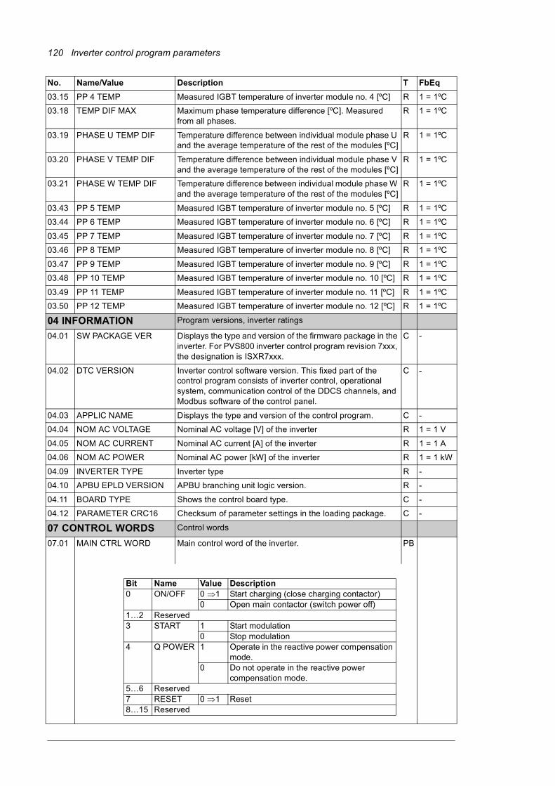
120 Inverter control program parameters
03.15 PP 4 TEMP Measured IGBT temperature of inverter module no. 4 [ºC] R 1 = 1ºC
03.18 TEMP DIF MAX Maximum phase temperature difference [ºC]. Measured from all phases.
R 1 = 1ºC
03.19 PHASE U TEMP DIF Temperature difference between individual module phase U and the average temperature of the rest of the modules [ºC]
R 1 = 1ºC
03.20 PHASE V TEMP DIF Temperature difference between individual module phase V and the average temperature of the rest of the modules [ºC]
R 1 = 1ºC
03.21 PHASE W TEMP DIF Temperature difference between individual module phase W and the average temperature of the rest of the modules [ºC]
R 1 = 1ºC
03.43 PP 5 TEMP Measured IGBT temperature of inverter module no. 5 [ºC] R 1 = 1ºC
03.44 PP 6 TEMP Measured IGBT temperature of inverter module no. 6 [ºC] R 1 = 1ºC
03.45 PP 7 TEMP Measured IGBT temperature of inverter module no. 7 [ºC] R 1 = 1ºC
03.46 PP 8 TEMP Measured IGBT temperature of inverter module no. 8 [ºC] R 1 = 1ºC
03.47 PP 9 TEMP Measured IGBT temperature of inverter module no. 9 [ºC] R 1 = 1ºC
03.48 PP 10 TEMP Measured IGBT temperature of inverter module no. 10 [ºC] R 1 = 1ºC
03.49 PP 11 TEMP Measured IGBT temperature of inverter module no. 11 [ºC] R 1 = 1ºC
03.50 PP 12 TEMP Measured IGBT temperature of inverter module no. 12 [ºC] R 1 = 1ºC
04 INFORMATION Program versions, inverter ratings
04.01 SW PACKAGE VER Displays the type and version of the firmware package in the inverter. For PVS800 inverter control program revision 7xxx, the designation is ISXR7xxx.
C -
04.02 DTC VERSION Inverter control software version. This fixed part of the control program consists of inverter control, operational system, communication control of the DDCS channels, and Modbus software of the control panel.
C -
04.03 APPLIC NAME Displays the type and version of the control program. C -
04.04 NOM AC VOLTAGE Nominal AC voltage [V] of the inverter R 1 = 1 V
04.05 NOM AC CURRENT Nominal AC current [A] of the inverter R 1 = 1 A
04.06 NOM AC POWER Nominal AC power [kW] of the inverter R 1 = 1 kW
04.09 INVERTER TYPE Inverter type R -
04.10 APBU EPLD VERSION APBU branching unit logic version. R -
04.11 BOARD TYPE Shows the control board type. C -
04.12 PARAMETER CRC16 Checksum of parameter settings in the loading package. C -
07 CONTROL WORDS Control words
07.01 MAIN CTRL WORD Main control word of the inverter. PB
No. Name/Value Description T FbEq
Bit Name Value Description0 ON/OFF 0 1 Start charging (close charging contactor)
0 Open main contactor (switch power off)1…2 Reserved3 START 1 Start modulation
0 Stop modulation4 Q POWER 1 Operate in the reactive power compensation
mode. 0 Do not operate in the reactive power
compensation mode.5…6 Reserved7 RESET 0 1 Reset8…15 Reserved

Inverter control program parameters 121
07.03 AUX CTRL WORD 2 Auxiliary control word for user-specified functions. PB
07.04 MPPT CMW Internal control word for the MPPT mode.
Note: This word can be used for monitoring only.
PB
08 STATUS WORDS Status words
08.01 MAIN STATUS WORD Main Status Word. PB
No. Name/Value Description T FbEq
Bit Value Description0 1 Enable the MPPT mode1 1 Enable DC level difference tracking2 1 Enable lost energy calculation3 1 Enable external DC reference for MPPT4 1 Close the DC switch5 Reserved6 1 Enable the DC contactor use7 1 Enable trip signal monitoring of the DC breaker8 1 Enable temperature monitoring of the inverter module9 1 Enable the Lost energy warning10 1 Enable the DC reference maximum / minimum warning11…15 Reserved
Bit Name Value STATE/Description0 RDY_ON 1 Ready to switch on = no fault1 RDY_RUN 1 Ready to operate = DC bus charged2 RDY_REF 1 Operation enabled
0 Operation inhibited3 TRIPPED 1 A fault occured in the inverter.4 HVRT 1 High voltage ride-through function is active5…6
Reserved
7 ALARM 1 A warning in the inverter.8 MODULATING 1 Inverter is modulating9 REMOTE 1 Control location: REMOTE
0 Control location: LOCAL10 NET OK 1 Grid voltage is OK
0 Grid voltage is lost11 LEVEL1 DIP 1 Low voltage ride-though function is active.12 Reserved13 CHARGING OR
RDY_RUNCombines bits 14 and 1.
1 Ready to operate or charging contactor closed14 CHARGING 1 Charging contactor closed15 Reserved

122 Inverter control program parameters
08.03 LIMIT WORD Limit word. PB
08.04 LIMIT WORD 2 A limit word to indicate active and reactive power limitations. PB -
08.05 DI STATUS WORD Inverter control unit digital input (DI) status word. This parameter shows the status of each digital input on the Inverter control unit and RDIO modules.
PB -
No. Name/Value Description T FbEq
Bit Name Value Description0 CURRENT PLIM 1 An internal current limit is limiting the active power. The limit
depends on the measured ambient temperature.1 EXTERNAL PLIM 1 An external active power limit in MCP parameter 31.16 POWER
LIMITING is limiting the active power.2 CAP REF LIMIT 1 Capacitive current reference above limit (24.22 IQ CAP LIMIT)3 IND REF LIMIT 1 Inductive current reference above limit (24.23 IQ IND LIMIT)4 DC REF MAX LIM 1 02.05 DC REF Q-CTRL is above the maximum DC voltage
reference.5 Q CUR LIM 1 Reactive current is limited because 01.06 LINE CURRENT has
reached the maximum allowed current.6 GRID POW LIM 1 Instantaneous active power limitation7 DC POW LIM 1 Active power from the grid is limited.8 POW FREQ LIM 1 Active power to the grid is limited because of grid over frequency.9 GRID FILT POW LIM 1 Active power to the grid is limited.10 HIGH UAC PLIM 1 Maximum active power is limited from grid overvoltage.11 MPPT PLIM 1 Maximum active power increase rate is limiting the active power.12 START POW LIM 1 Active power ramp-up after the start is limiting the active power.13 POWER STOP RAMP 1 Active and/or reactive power is limited during a controlled stop.14 LVRT RETURN PLIM 1 Return ramp after Low voltage ride-through is limiting the active
power.15 U FREQ PLIM 1 Active power is limited according to the grid underfrequency
characteristic curve.
Bit Value Description0 1 Inductive reactive power reference is limited by the Q(P) characteristic curve.1 1 Capacitive reactive power reference is limited by the Q(P) characteristic curve.
Bit Name Description0 DI1 Inverter control unit DI1 status, feedback of inverter cabinet fans and LCL fans1 DI2 Inverter control unit DI2 status2 DI3 Inverter control unit DI3 status, feedback of AC contactor K1.13 DI4 Inverter control unit DI4 status4 DI5 Inverter control unit DI5 status5 DI6 Inverter control unit DI6 status6 DI7 (DIIL) Inverter control unit DI7 (DIIL) status7 EXT1_DI1 RDIO module 1, DI1 status, feedback of DC contactor K2.18 EXT1_DI2 RDIO module 1, DI2 status, feedback of DC contactor K2.29 EXT1_DI3 RDIO module 1, DI3 status, state of optional grid monitoring relay10 EXT2_DI1 RDIO module 2, DI1 status, feedback of AC contactor K1.211 EXT2_DI2 RDIO module 2, DI2 status, feedback of AC contactor K1.312 EXT2_DI3 RDIO module 2, DI3 status, feedback of DC contactor K2.313…15 Reserved

Inverter control program parameters 123
08.06 MPPT STATUS MPPT status word. See also 08.04 PVA STATES in the master control program (page 59).
PB -
08.07 GRID CODE STATUS Status word for miscellaneous grid code related information.
No. Name/Value Description T FbEq
Bit Name Value Description0 MPPT 1 Inverter running in the MPPT mode. See parameter 39.01
MPPT CONTROL (page 145).1 LOCAL MODE 1 Inverter in the local control mode, MPPT disabled, DC switch
open.2 START MPPT 1 Start command received; DC pre-charge or DC switch closure
in progress before entering the MPPT mode.3 RELAY INIT 0 Inverter unit initializing after power-on. Master control program
remains in the STANDBY state.1 Inverter unit ready.
4 DC SWITCH STA 1 DC switch is closed.5 GRIDMON RELAY RESTART 1 Grid monitoring relay has signalled a network failure. Inverter
unit parametrized to restart after delay.6 LOST ENERGY 1 Lost energy calculation active. Power limit set lower than
PVS800 nominal power.7 START ENA 1 Start is enabled by cut-in conditions. See parameters
44.18…44.23 (page 159).8 DC REF MIN 1 MPPT has reached the minimum DC reference. Check 39.05
MPPT DC REF MIN (page 145).9 DC REF MAX 1 MPPT has reached the maximum DC reference. Check
parameter 39.04 MPPT DC REF MAX (page 145).10 DC CTRL LIM 1 External DC reference cannot be maintained because of
power limiting.11 Reserved12 VOLTAGE SUPPRESSION 1 Grid voltage rise suppression -function is active.13 ANTI-ISLAND RESTART 1 Anti-island restart delay is ongoing, the inverter operation is
disabled until the delay has passed.14 Q POW RUN 1 Inverter is running in the Q POWER state.15 Reserved
Bit Name Value STATE/Description0 O FREQ DELAY 1 Delay counting in Active power limitation from grid
overfrequency is ongoing.1 O FREQ RETURN RAMP 1 Active power limit is restoring with a ramp from the grid
overfrequency transient.2 U FREQ DELAY 1 Delay counting in Active power limitation from grid
underfrequency is ongoing.3 U FREQ RETURN RAMP 1 Active power limit is restoring with a ramp from the grid
underfrequency transient.4 U FREQ ACTIVE 1 Grid underfrequency transient is ongoing.5 O FREQ ACTIVE 1 Grid overfrequency transient is ongoing.

124 Inverter control program parameters
08.08 ISLAND STATUS Anti-island status word. PB -
08.22 INT CONFIG WORD 16-bit data word. Number of inverter units recognized by the control program during PPCC link initialization.
Bit 0 = INT1 = Inverter unit 1 INT board…
Bit 2 = INT3 = Inverter unit 3 INT board
PB
08.31 AINT TYPE
Shows the AINT/AGDR configuration data read from the inverter module specified by parameter 16.11 PBU CH AINT CHK.
The control program reads the configuration data from all parallel-connected inverter modules at power-up. All modules must return the same configuration data. In case of a mismatch, a fault is generated.
The configuration data shown by 08.31 AINT TYPE is coded as follows:
For example, if this parameter displays the value 74231, the module selected by 16.11 has an AINT-24 board, and the du/dt configuration of its AGDR board is 7.
I
No. Name/Value Description T FbEq
Bit Name Value STATE/Description0 PEAK DETECT ENABLE 1 Anti-island peak detection is enabled1 ADAPT DETECT ENABLE 1 Anti-island adaptive level detection is enabled2 CONST DETECT ENABLE 1 Anti-island constant level detection is enabled3...4 Reserved5 PEAK DETECTED 1 The last anti-island fault was caused by peak detection6 ADAPT LEVEL DETECTED 1 The last anti-island fault was caused by adaptive level
detection7 CONST LEVEL DETECTED 1 The last anti-island fault was caused by constant level
detection
AINT board type (AINT-…)
Configuration dataAGDR du/dt
configurationAINT
IDAINT
ASIC ID01(C)
0 or 7
1 21502(C) 1 231
11/12/14(C) 2 21514D 2 23124 4 231
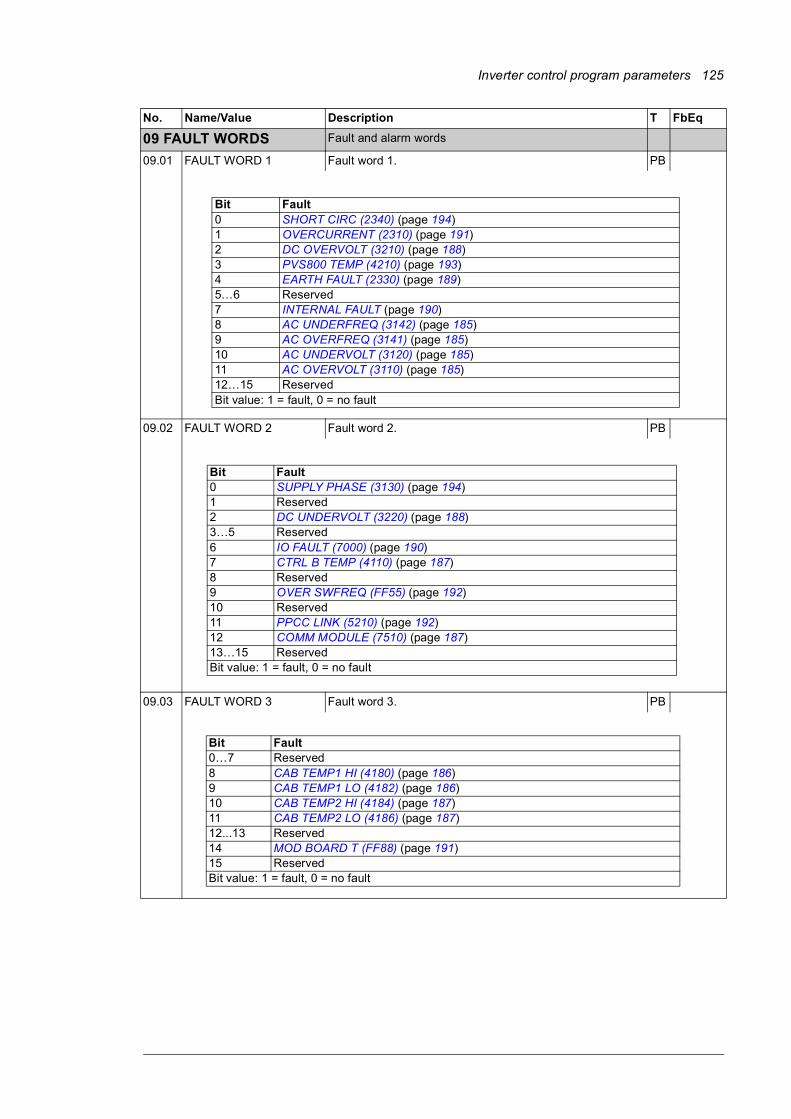
Inverter control program parameters 125
09 FAULT WORDS Fault and alarm words
09.01 FAULT WORD 1 Fault word 1. PB
09.02 FAULT WORD 2 Fault word 2. PB
09.03 FAULT WORD 3 Fault word 3. PB
No. Name/Value Description T FbEq
Bit Fault0 SHORT CIRC (2340) (page 194)1 OVERCURRENT (2310) (page 191)2 DC OVERVOLT (3210) (page 188)3 PVS800 TEMP (4210) (page 193)4 EARTH FAULT (2330) (page 189)5…6 Reserved7 INTERNAL FAULT (page 190)8 AC UNDERFREQ (3142) (page 185)9 AC OVERFREQ (3141) (page 185)10 AC UNDERVOLT (3120) (page 185)11 AC OVERVOLT (3110) (page 185)12…15 ReservedBit value: 1 = fault, 0 = no fault
Bit Fault0 SUPPLY PHASE (3130) (page 194)1 Reserved2 DC UNDERVOLT (3220) (page 188)3…5 Reserved6 IO FAULT (7000) (page 190)7 CTRL B TEMP (4110) (page 187)8 Reserved9 OVER SWFREQ (FF55) (page 192)10 Reserved11 PPCC LINK (5210) (page 192)12 COMM MODULE (7510) (page 187)13…15 ReservedBit value: 1 = fault, 0 = no fault
Bit Fault0…7 Reserved8 CAB TEMP1 HI (4180) (page 186)9 CAB TEMP1 LO (4182) (page 186)10 CAB TEMP2 HI (4184) (page 187)11 CAB TEMP2 LO (4186) (page 187)12...13 Reserved14 MOD BOARD T (FF88) (page 191)15 ReservedBit value: 1 = fault, 0 = no fault

126 Inverter control program parameters
09.04 ALARM WORD 1 Alarm word 1. PB
09.10 PV FLT ALM WORD Fault/Alarm word. PB
09.11 SUPPLY FAULT WORD Inverter unit fault word. If the inverter unit consists of parallel connected modules, a fault is indicated by this word if it is present in any module.
PB
No. Name/Value Description T FbEq
Bit Fault0 CAB TEMP1 HI (4181) (page 186)1 CAB TEMP1 LO (4183) (page 187)2…6 Reserved7 CAB TEMP2 HI (4185) (page 187)8 CAB TEMP2 LO (4187) (page 187)9 Reserved10 EXT ANALOG IO (7081) (page 189)11...13 Reserved14 MOD BOARD T (FF92) (page 191)15 ReservedBit value: 1 = alarm, 0 = no alarm
Bit Fault/Alarm0 GRID MON FLT (8189) (page 190)1 Reserved2 REVERSE POW (8187) (page 193) (peak)3 DC SWITCH LEV (818C) (page 188)4 DC SWITCH POS (818D) (page 188)5 REVERSE POW (8187) (page 193) (level)6 Reserved7 LOST ENERGY (8192) (page 190)8 GRID MON ALM (8191) (page 190)9 PVS&PANEL DC (32A8) (page 192)10 Reserved11 ANTI-ISLAND (8193) (page 186)12 DCREF MIN RNG (32AB) (page 188)13 DCREF MAX RNG (32AC) (page 188)14…15 ReservedBit value: 1 = fault/alarm, 0 = no fault/alarm
Bit Fault0 CHARGING FLT (3230) (page 187)1 OVERCURRENT (2310) (page 191)2 EXT EVENT DI5 (9085) (page 189)3 PVS800 TEMP (4210) (page 193)4 EXT EVENT DI4 (9084) (page 189)5 DI1 (9088) (page 188)6 MAIN CNT FLT (FF17) (page 191)7 SHORT CIRC (2340) (page 194)8 INTERNAL FAULT (page 190)9 NET VOLT FLT (3100)/(32A2) (page 191) or RT NET LOST (32A1) (page 193)10 COMM MODULE (7510) (page 187)11 EXT EVNT DI7 (908E) (page 190)12 EARTH FAULT (2387) (page 189)13 Reserved14 DC UNDERVOLT (3220) (page 188)15 DC OVERVOLT (3210) (page 188)Bit value: 1 = fault, 0 = no fault

Inverter control program parameters 127
09.12 SUPPLY ALARM WORD Inverter unit alarm word. PB
09.13 CURRENT UNBALANCE Current unbalance fault word. PB
09.14 OVERCURRENT FAULT Overcurrent fault word. PB
09.15 SHORT CIRC FAULT Short circuit fault word. PB
No. Name/Value Description T FbEq
Bit Fault0 COMM MODULE (7510) (page 187)1 PANEL LOST (5300) (page 192)2 DI1 (9088) (page 188)3 Reserved4 PVS800 TEMP (4294) (page 193)5...7 Reserved8 QLIM PVS TMP (44A2) (page 193)9 RUN DISABLED (FFAC) (page 193)10 NET LOST (32A3) (page 191)11 EXT EVNT DI7 (908E) (page 190)12 RECHARGE ALM (3250) (page 193)13 EXT EVNT DI4 (908B) (page 189)14 EXT EVNT DI5 (908C) (page 190)15 ReservedBit value: 1 = alarm, 0 = no alarm
Bit Fault0 CUR UNBAL 1 (23E0) (page 187)1 CUR UNBAL 2 (23E1) (page 187)2 CUR UNBAL 3 (23E2) (page 187)3…15 ReservedBit value: 1 = fault, 0 = no fault
Bit Fault0 OVERCURR 1 (23A0) (page 191)1 OVERCURR 2 (23A1) (page 191)2 OVERCURR 3 (23A2) (page 191)3…15 ReservedBit value: 1 = fault, 0 = no fault
Bit Fault0 SC INV 1 U (23B0), SC INV 1 V (23B1) or SC INV 1 W (23B2) (page 194)1 SC INV 2 U (23B3), SC INV 2 V (23B4) or SC INV 2 W (23B5) (page 194)2 SC INV 3 U (23B6), SC INV 3 V (23B7) or SC INV 3 W (23B8) (page 194)3…11 Reserved12 Short circuit in phase U of the faulted module13 Short circuit in phase V of the faulted module14 Short circuit in phase W of the faulted module15 ReservedBit value: 1 = fault, 0 = no fault
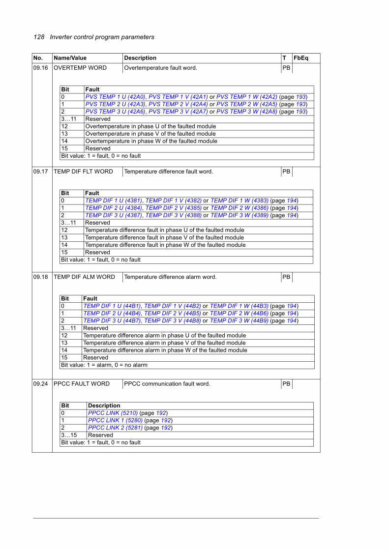
128 Inverter control program parameters
09.16 OVERTEMP WORD Overtemperature fault word. PB
09.17 TEMP DIF FLT WORD Temperature difference fault word. PB
09.18 TEMP DIF ALM WORD Temperature difference alarm word. PB
09.24 PPCC FAULT WORD PPCC communication fault word. PB
No. Name/Value Description T FbEq
Bit Fault0 PVS TEMP 1 U (42A0), PVS TEMP 1 V (42A1) or PVS TEMP 1 W (42A2) (page 193)1 PVS TEMP 2 U (42A3), PVS TEMP 2 V (42A4) or PVS TEMP 2 W (42A5) (page 193)2 PVS TEMP 3 U (42A6), PVS TEMP 3 V (42A7) or PVS TEMP 3 W (42A8) (page 193)3…11 Reserved12 Overtemperature in phase U of the faulted module13 Overtemperature in phase V of the faulted module14 Overtemperature in phase W of the faulted module15 ReservedBit value: 1 = fault, 0 = no fault
Bit Fault0 TEMP DIF 1 U (4381), TEMP DIF 1 V (4382) or TEMP DIF 1 W (4383) (page 194)1 TEMP DIF 2 U (4384), TEMP DIF 2 V (4385) or TEMP DIF 2 W (4386) (page 194)2 TEMP DIF 3 U (4387), TEMP DIF 3 V (4388) or TEMP DIF 3 W (4389) (page 194)3…11 Reserved12 Temperature difference fault in phase U of the faulted module13 Temperature difference fault in phase V of the faulted module14 Temperature difference fault in phase W of the faulted module15 ReservedBit value: 1 = fault, 0 = no fault
Bit Fault0 TEMP DIF 1 U (44B1), TEMP DIF 1 V (44B2) or TEMP DIF 1 W (44B3) (page 194)1 TEMP DIF 2 U (44B4), TEMP DIF 2 V (44B5) or TEMP DIF 2 W (44B6) (page 194)2 TEMP DIF 3 U (44B7), TEMP DIF 3 V (44B8) or TEMP DIF 3 W (44B9) (page 194)3…11 Reserved12 Temperature difference alarm in phase U of the faulted module13 Temperature difference alarm in phase V of the faulted module14 Temperature difference alarm in phase W of the faulted module15 ReservedBit value: 1 = alarm, 0 = no alarm
Bit Description0 PPCC LINK (5210) (page 192)1 PPCC LINK 1 (5280) (page 192)2 PPCC LINK 2 (5281) (page 192)3…15 ReservedBit value: 1 = fault, 0 = no fault

Inverter control program parameters 129
09.25 POWERFAIL FAULT AINT board power failure word. PB
09.30 FAULT CODE 1 LAST Fieldbus code of the latest alarm/fault. See chapter Fault tracing.
The fault buffer can be reset using parameter 16.16 RESET FLT/ALM BUF (page 134).
PB
09.31 FAULT CODE 2 LAST Fieldbus code of the 2nd latest alarm/fault
09.32 FAULT CODE 3 LAST Fieldbus code of the 3rd latest alarm/fault
09.33 FAULT CODE 4 LAST Fieldbus code of the 4th latest alarm/fault
09.34 FAULT CODE 5 LAST Fieldbus code of the 5th latest alarm/fault
09.35 FAULT CODE 6 LAST Fieldbus code of the 6th latest alarm/fault
09.36 FAULT CODE 7 LAST Fieldbus code of the 7th latest alarm/fault
09.37 FAULT CODE 8 LAST Fieldbus code of the 8th latest alarm/fault
09.38 FAULT CODE 9 LAST Fieldbus code of the 9th latest alarm/fault
09.39 FAULT CODE 10 LAST Fieldbus code of the 10th latest alarm/fault
No. Name/Value Description T FbEq
Bit Description0 POWERFAIL (3381) (page 192)1 POWERF INV 1 (3382) (page 192)2 POWERF INV 2 (3383) (page 192)3…15 ReservedBit value: 1 = fault, 0 = no fault

130 Inverter control program parameters
Parameter groups 11…99No. Name/Value Description Def. T FbEq
13 ANALOGUE INPUTS
Analog input signal processing
13.03 FILTER AI1 Defines the filter time constant for analog input AI1. The hardware filter time constant (with the RMIO board) is fixed to 20 ms.
1000 ms R
0…30000 ms Filter time constant 1 = 1 ms
13.07 FILTER AI2 Defines the filter time constant for analog input AI2. The hardware filter time constant (with the RMIO board) is fixed to 20 ms.
1000 ms R
0…30000 ms Filter time constant. See parameter 13.03 FILTER AI1.
1 = 1 ms
13.11 FILTER AI3 Defines the filter time constant for analog input AI3. The hardware filter time constant (with the RMIO board) is 20 ms.
1000 ms R
0…30000 ms Filter time constant. See parameter 13.03 FILTER AI1.
1 = 1 ms
14 DIGITAL OUTPUTS Relay output control
14.06 EXT1 DO1 SEL Selects the source for status information indicated through digital output DO1 on I/O extension module 1.
151.04 b4 P
-255.255.31 … +255.255.31 / C. -32768 … C. 32767
Parameter index or a constant value:
- Parameter pointer: Inversion, group, index and bit fields. The bit number is effective only for blocks handling Boolean inputs.
- Constant value: Inversion and constant fields. Inversion field must have value C to enable the constant setting.
Example: The state of digital input DI2 is connected to input 1 as follows:
- Set the source selection parameter (57.06) to +01.15.01. (The adaptive program stores the state of digital input DI2 to bit 1 of actual signal 01.15.)
- If you need an inverted value, switch the sign of the pointer value (-01.15.01).
14.07 EXT1 DO2 SEL Selects the source for status information indicated through digital output DO2 on I/O extension module 1.
151.04 b4 P
See parameter 14.06 EXT1 DO1 SEL.
14.09 EXT2 DO2 SEL Selects the source for status information indicated through digital output DO2 on I/O extension module 2.
151.04 b4 P
See parameter 14.06 EXT1 DO1 SEL.
63
%
100
Tt
Filtered Signal
Unfiltered Signal O = I · (1 - e-t/T)
I = filter input (step)O = filter outputt = timeT = filter time constant

Inverter control program parameters 131
15 ANALOGUE OUTPUTS
Output signal processing
15.01 ANALOGUE OUTPUT 1
Connects a signal to analog output AO1. 15811 I
0…30000 Example: Parameter index 109 denotes signal 01.09 POWER.
1 = 1
15.02 INVERT AO1 Activates analog output AO1 signal inversion. NO B
NO Inversion inactive. Minimum signal value corresponds to the minimum output value.
0
YES Inversion active. Maximum signal value corresponds to the minimum output value.
1
15.03 MINIMUM AO1 Defines the minimum value for analog output AO1.
0 mA I
0 mA Zero milliamperes 1
4 mA Four milliamperes 2
10 mA Ten milliamperes 3
15.04 FILTER AO1 Defines the filter time constant for analog output AO1.
5 s R
0.00…10.00 s Filter time constant 100 = 1.00 s
15.05 SCALE AO1 Defines the nominal value of the signal connected to analog output AO1. See parameter 15.01 ANALOGUE OUTPUT 1. The value corresponds to 20 mA at the output.
Example: Parameter 01.06 LINE CURRENT is indicated through analog output AO1. The nominal value of line current is 100 A. This parameter is set to 100 to match the nominal value (100 A) with the analog output signal maximum (20 mA).
100 R
0…65536 Real value 1 = 1
15.06 ANALOGUE OUTPUT 2
Connects a measured signal to analog output AO2.
0 I
0…30000 Parameter index 109 denotes signal 01.09 POWER.
1 = 1
15.07 INVERT AO2 Activates analog output AO2 signal inversion. NO B
NO Inversion inactive. Minimum signal value corresponds to the minimum output value.
0
YES Inversion active. Maximum signal value corresponds to the minimum output value.
1
15.08 MINIMUM AO2 Defines the minimum value for analog output AO2.
0 mA I
0 mA Zero milliamperes 1
4 mA Four milliamperes 2
10 mA Ten milliamperes 3
15.09 FILTER AO2 Defines the filter time constant for analog output AO2. See parameter 15.04 FILTER AO1.
0.1 s R
0.00…10.00 s Filter time constant 100 = 1.00 s
No. Name/Value Description Def. T FbEq
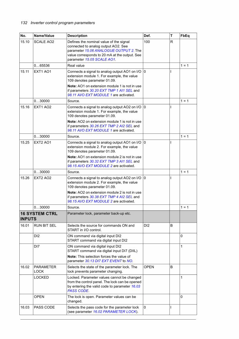
132 Inverter control program parameters
15.10 SCALE AO2 Defines the nominal value of the signal connected to analog output AO2. See parameter 15.06 ANALOGUE OUTPUT 2. The value corresponds to 20 mA at the output. See parameter 15.05 SCALE AO1.
100 R
0…65536 Real value 1 = 1
15.11 EXT1 AO1 Connects a signal to analog output AO1 on I/O extension module 1. For example, the value 109 denotes parameter 01.09.
Note: AO1 on extension module 1 is not in use if parameters 30.20 EXT TMP 1 AI1 SEL and 98.11 AI/O EXT MODULE 1 are activated.
0 I
0…30000 Source. 1 = 1
15.16 EXT1 AO2 Connects a signal to analog output AO2 on I/O extension module 1. For example, the value 109 denotes parameter 01.09.
Note: AO2 on extension module 1 is not in use if parameters 30.26 EXT TMP 2 AI2 SEL and 98.11 AI/O EXT MODULE 1 are activated.
0 I
0…30000 Source. 1 = 1
15.25 EXT2 AO1 Connects a signal to analog output AO1 on I/O extension module 2. For example, the value 109 denotes parameter 01.09.
Note: AO1 on extension module 2 is not in use if parameters 30.32 EXT TMP 3 AI1 SEL and 98.15 AI/O EXT MODULE 2 are activated.
0 I
0…30000 Source. 1 = 1
15.26 EXT2 AO2 Connects a signal to analog output AO2 on I/O extension module 2. For example, the value 109 denotes parameter 01.09.
Note: AO2 on extension module 2 is not in use if parameters 30.38 EXT TMP 4 AI2 SEL and 98.15 AI/O EXT MODULE 2 are activated.
0 I
0…30000 Source. 1 = 1
16 SYSTEM CTRL INPUTS
Parameter lock, parameter back-up etc.
16.01 RUN BIT SEL Selects the source for commands ON and START in I/O control.
DI2 B
DI2 ON command via digital input DI2START command via digital input DI2
0
DI7 ON command via digital input DI2START command via digital input DI7 (DIIL)
Note: This selection forces the value of parameter 30.13 DI7 EXT EVENT to NO.
1
16.02 PARAMETER LOCK
Selects the state of the parameter lock. The lock prevents parameter changing.
OPEN B
LOCKED Locked. Parameter values cannot be changed from the control panel. The lock can be opened by entering the valid code to parameter 16.03 PASS CODE.
1
OPEN The lock is open. Parameter values can be changed.
0
16.03 PASS CODE Selects the pass code for the parameter lock (see parameter 16.02 PARAMETER LOCK).
0 I
No. Name/Value Description Def. T FbEq
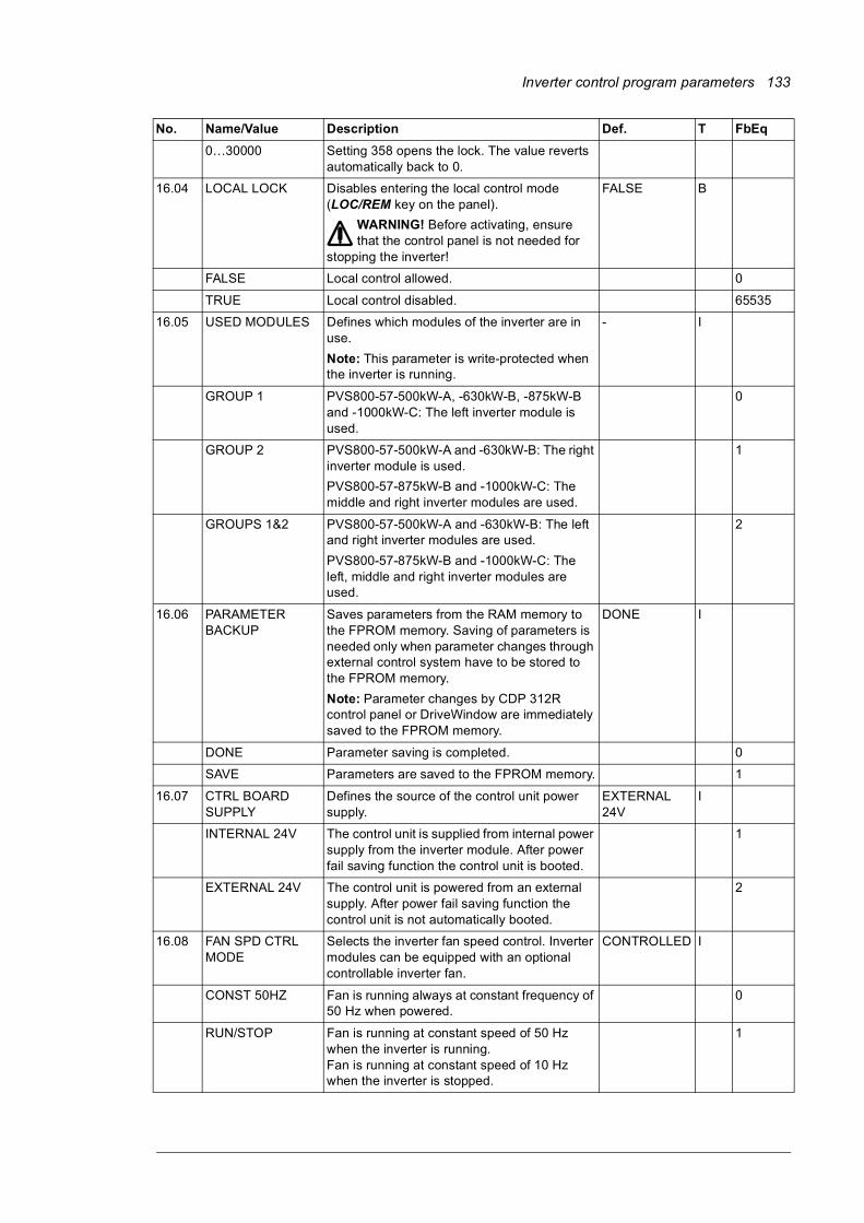
Inverter control program parameters 133
0…30000 Setting 358 opens the lock. The value reverts automatically back to 0.
16.04 LOCAL LOCK Disables entering the local control mode (LOC/REM key on the panel).
WARNING! Before activating, ensure that the control panel is not needed for
stopping the inverter!
FALSE B
FALSE Local control allowed. 0
TRUE Local control disabled. 65535
16.05 USED MODULES Defines which modules of the inverter are in use.
Note: This parameter is write-protected when the inverter is running.
- I
GROUP 1 PVS800-57-500kW-A, -630kW-B, -875kW-B and -1000kW-C: The left inverter module is used.
0
GROUP 2 PVS800-57-500kW-A and -630kW-B: The right inverter module is used.
PVS800-57-875kW-B and -1000kW-C: The middle and right inverter modules are used.
1
GROUPS 1&2 PVS800-57-500kW-A and -630kW-B: The left and right inverter modules are used.
PVS800-57-875kW-B and -1000kW-C: The left, middle and right inverter modules are used.
2
16.06 PARAMETER BACKUP
Saves parameters from the RAM memory to the FPROM memory. Saving of parameters is needed only when parameter changes through external control system have to be stored to the FPROM memory.
Note: Parameter changes by CDP 312R control panel or DriveWindow are immediately saved to the FPROM memory.
DONE I
DONE Parameter saving is completed. 0
SAVE Parameters are saved to the FPROM memory. 1
16.07 CTRL BOARD SUPPLY
Defines the source of the control unit power supply.
EXTERNAL 24V
I
INTERNAL 24V The control unit is supplied from internal power supply from the inverter module. After power fail saving function the control unit is booted.
1
EXTERNAL 24V The control unit is powered from an external supply. After power fail saving function the control unit is not automatically booted.
2
16.08 FAN SPD CTRL MODE
Selects the inverter fan speed control. Inverter modules can be equipped with an optional controllable inverter fan.
CONTROLLED I
CONST 50HZ Fan is running always at constant frequency of 50 Hz when powered.
0
RUN/STOP Fan is running at constant speed of 50 Hz when the inverter is running.Fan is running at constant speed of 10 Hz when the inverter is stopped.
1
No. Name/Value Description Def. T FbEq

134 Inverter control program parameters
CONTROLLED The speed of the fan is determined from the IGBT temperature vs. the fan speed curve when the inverter is running. The speed range is 25…55 Hz.Fan is running at constant speed of 10 Hz when the inverter is stopped.
2
16.09 RESET COUNTER Resets the selected counter. NO I
NO No reset. The value automatically restores to NO after a reset.
1
BREAKER Main contactor/breaker counter reset (01.30 BREAKER COUNTER)
2
FAN ON TIME Inverter cooling fan running time counter reset (01.31 FAN ON-TIME)
3
KWH kWh counter reset (01.14 KWH SUPPLY, 01.16 KWH MOTORING and 01.17 KWH GENERATING)
4
16.10 INT CONFIG USER Defines a number of parallel connected inverter modules which the inverter shall operate.
Note: In caseof reduced run function, a value of this parameter must be changed.
0 R
1…3 Number of parallel connected inverter modules 1 = 1
16.11 PBU CH AINT CHK Selects the inverter module whose AINT/AGDR configuration data is shown by 08.31 AINT TYPE.
1 I
1…12 Inverter module number. 1 = 1
16.12 RESET RUN-TIME Resets parameters 01.38 RUN-TIME. NO I
NO Reset done or not requested. 0
YES Reset 01.38 RUN-TIME. 65535
16.14 POWER SIGN CHANGE
Changes the sign of the power. YES B
NO No power sign change 0
YES Power sign changed: Signs of signals 01.08 and 01.09 are inverted.
1
16.15 START MODE Selects the start mode. LEVEL B
LEVEL Starts inverter by level of control command. Control command is selected by parameter 98.01 COMMAND SEL and 98.02 COMM. MODULE.
WARNING! After a fault reset, the inverter will start if the start signal is on.
0
EDGE Starts inverter by edge of control command. Control command is selected by parameter 98.01 COMMAND SEL and 98.02 COMM. MODULE.
1
16.16 RESET FLT/ALM BUF
Clears parameters 09.30…09.39. DONE I
DONE Clearing done or not requested. 0
RESET Clears the 10 latest alarm/fault codes. 65535
16.17 RESET DC BRK CNT
Clears master control program parameter 01.31 DC BREAKER COUNTR.
OFF I
OFF Clearing done or not requested. 0
No. Name/Value Description Def. T FbEq
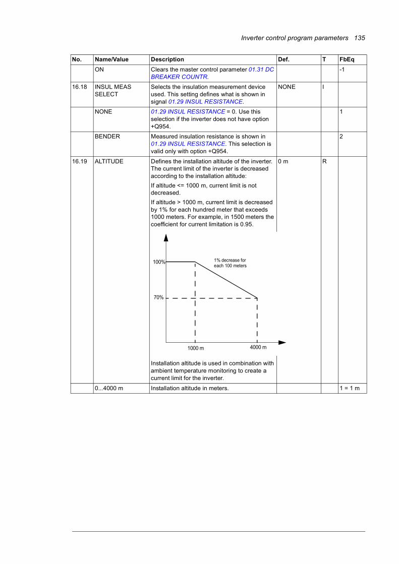
Inverter control program parameters 135
ON Clears the master control parameter 01.31 DC BREAKER COUNTR.
-1
16.18 INSUL MEAS SELECT
Selects the insulation measurement device used. This setting defines what is shown in signal 01.29 INSUL RESISTANCE.
NONE I
NONE 01.29 INSUL RESISTANCE = 0. Use this selection if the inverter does not have option +Q954.
1
BENDER Measured insulation resistance is shown in 01.29 INSUL RESISTANCE. This selection is valid only with option +Q954.
2
16.19 ALTITUDE Defines the installation altitude of the inverter. The current limit of the inverter is decreased according to the installation altitude:
If altitude <= 1000 m, current limit is not decreased.
If altitude > 1000 m, current limit is decreased by 1% for each hundred meter that exceeds 1000 meters. For example, in 1500 meters the coefficient for current limitation is 0.95.
Installation altitude is used in combination with ambient temperature monitoring to create a current limit for the inverter.
0 m R
0...4000 m Installation altitude in meters. 1 = 1 m
No. Name/Value Description Def. T FbEq
100%
70%
1000 m 4000 m
1% decrease for each 100 meters

136 Inverter control program parameters
18 LED PANEL CTRL The Inverter Monitoring Display has a LED bar to show an absolute real type value.
The source and the scale of the display signal are defined by this parameter group.
Note: If the Inverter Monitoring Display and CDP 312R Control Panel are used together, actual signal 01.26 LED PANEL OUTP must be the first signal in the CDP 312R Actual Signal Display mode. Otherwise the LED bar of the Inverter Monitoring Display display will show an incorrect value. The ISXR73XX panel link ID number must be 1, see How to select a control unit and change its panel link ID number.
18.01 LED PANEL OUTPUT
Selects the signal source for the Inverter Monitoring Display.
Example: To show signal 01.09 POWER on the display, set this parameter to 109.
109 I
0…30000 Parameter index 109 denotes signal 01.09 POWER.
18.02 SCALE PANEL Defines the value of the signal selected by parameter 18.01 LED PANEL OUTPUT which corresponds to 100% on the LED bar display.
Example: Signal 01.05 FREQUENCY is shown on the LED display:
At 50 Hz the LED display indicates full value (100%) when: Parameter 18.01 is set to 105.Parameter 18.02 is set to 5000 (= 100 · 50 = 5000, where 100 is the integer scale (FbEq) for signal 01.05).
100 R
0…65536 Scaling factor 1 = 1
19 DATA STORAGE Parameters for receiving information from or sending to an external control system. The parameters are unconnected and they can be used for linking, testing and commissioning purposes.
19.01 DATA 1 Stores data written from a user-defined source. 0 R
32768…+32767 Data value 1 = 1
… … … … … …
19.08 DATA 8 See parameter 19.01. 0 R
32768…+32767 Data value 1 = 1
23 DC VOLT REF DC voltage reference
23.01 DC VOLT REF Shows the DC voltage reference. By default, the reference is received from the MPPT algorithm; an external reference can be selected using parameter 39.08 ENA EXT DC REF (see page 145).
Varies R
V DC voltage reference. The range is limited by parameters 39.05 MPPT DC REF MIN and 39.04 MPPT DC REF MAX. (At start, the maximum DC reference is 875 V.)
1 = 1 V
No. Name/Value Description Def. T FbEq
0 50 100 150%

Inverter control program parameters 137
24 REACTIVE POWER
Reactive power settings
24.01 Q POWER REF Shows reactive power reference in percent of inverter nominal power.
0% R
-100…+100% Reactive power reference.
• Positive value denotes capacitive load.
• Negative value denotes inductive load.
100 = 1%
24.02 Q POWER REF2 MCP 24.02 Q POWER REF (72) 0 I
24.03 Q POWER REF2 SEL
MCP 24.03 Q POWER REF SEL (74) kVAr I
24.04 Q POWER REF ADD
Defines an additional reactive power reference value, which is added to 24.02 Q POWER REF2.
0 kVAr R
-120…120% Additional reactive power reference in percent of 04.06 NOM AC POWER
1 = 1 kVAr
24.05 Q POWER STOP DLY
Defines a delay for stopping the inverter in the Q POWER state. When the reactive power reference is below the level defined in parameter 24.06 Q POW ZERO MARGIN for this time delay, the inverter is stopped and the AC contactor opened. The inverter starts again when the reactive power reference reaches the defined level.
60 s R
0…1000000 s Stop delay 1 = 1 s
24.06 Q POW ZERO MARGIN
Defines a margin for the zero reactive power reference in the Q POWER state. See parameter 24.05 Q POWER STOP DLY.
1% R
0…100% Margin for zero reactive power reference 100 = 1%
24.08 COS PHI CAP LIMIT
Defines the minimum allowed cosine phi at the capacitive side. Cosine phi is always greater than or equal to this value.
0.0 R
0…1 Cosine phi limit at the capacitive side 100 = 1.0
24.09 COS PHI IND LIMIT
Defines the minimum allowed cosine phi at the inductive side. Cosine phi is always greater than or equal to this value.
0.0 R
0…1 Cosine phi limit at the inductive side 100 = 1.0
24.10 LOCK-IN POWER Defines the lock-in power level for Q(U) control. The active power has to be greater than this level before the Q(U) control starts producing non-zero reactive power reference.
0% R
0…100% Lock-in value for active power 100 = 1%
24.11 LOCK-OUT POWER
Defines the lock-out power level for Q(U) control. If the active power is below this level, the reactive power reference from the Q(U) control will be zero.
Note: The lock-out power level has to be smaller than the lock-in power level (24.10 LOCK-IN POWER).
0% R
0…100% Lock-out value for active power 100 = 1%
No. Name/Value Description Def. T FbEq

138 Inverter control program parameters
24.15 AC-CTR GAIN Defines the relative gain of the AC voltage controller.
For example, if the gain is set to 1, a 10% change in the error value (reference - actual value) causes the AC voltage controller output to change by 10%.
2 R
0…8 AC voltage controller gain 1 = 1
24.16 AC-CTR INTEG TIME
Defines the integration time of the AC voltage controller.
1 s R
0.1…1000 s AC voltage controller integration time 10 = 1 s
24.17 AC-CTR OFFSET Defines an offset value that can be used to manipulate the UAC reference input. The offset
is added to the reference given by the user.
With zero offset, the reference range 9000…10000…11000 corresponds to 90…100…110% of nominal voltage.
With an offset of 1000, the reference range 8000…9000…10000 corresponds to 90…100…110% of nominal voltage.
0 I
-32768…32767 AC voltage controller offset 1 = 1
24.18 AC-CTR LOW LIMIT
Defines the minimum reactive power reference value at the AC controller output. A negative value denotes inductive reactive power.
-100% I
-120…0% Minimum reactive power reference value at the AC controller output
100 = 1%
24.19 AC-CTR HIGH LIMIT
Defines the maximum reactive power reference value at the AC controller output. A positive value denotes capacitive reactive power.
100% I
0…120% Maximum reactive power reference value at the AC controller output
100 = 1%
24.20 Q POWER CAP LIMIT
Defines the maximum capacitive (leading) reactive power that the inverter can feed to the grid.
100% R
0…120% Limit in percent of 04.06 NOM AC POWER 100 = 1%
24.21 Q POWER IND LIMIT
Defines the maximum inductive (lagging) reactive power that the inverter can take from the grid.
100% R
0…120% Limit in percent of 04.06 NOM AC POWER 100 = 1%
24.22 IQ CAP LIMIT Capacitive current reference limit. If the capacitive current reference is higher than this limit, bit 2 of 08.03 LIMIT WORD is set.
Note: An active reduced run function rescales the limit.
100% R
0…200% Capacitive current reference limit in percent of 04.05 NOM AC CURRENT
1 = 1%
24.23 IQ IND LIMIT Inductive current reference limit. If the inductive current reference is higher than this limit, bit 3 of 08.03 LIMIT WORD is set.
Note: An active reduced run function rescales the limit.
100% R
0…200% Inductive current reference limit in percent of 04.05 NOM AC CURRENT
1 = 1%
No. Name/Value Description Def. T FbEq

Inverter control program parameters 139
24.25 Q(U) SLOPE Defines the slope for Q(U) control reference calculation. If the grid voltage differs from the nominal value defined by parameter 24.02 Q POWER REF2, then Q(U) control feeds reactive power.
Amount of reactive power can be defined from the formula below:
24.25 Q(U) SLOPE x UAC change
If UAC is less than nominal, capacitive power is generated. If UAC is above nominal, inductive power is generated. See also parameters 24.02, 24.26...24.28.
4.17%/V R
0…20 %/V Q(U) slope 100 = 1 %/V
24.26 Q(U) DEAD BAND Defines a dead band for Q(U) control. If the grid voltage stays inside the dead band area, Q(U) control is not active.
0 V R
0…100 V Voltage hysteresis 100 = 1 V
24.27 Q(U) TIME DELAY Defines a time delay for Q(U) control. Q(U) control is active when the grid voltage is outside the hysteresis area longer than this time delay.
0 s R
0…3600 s Time delay 100 = 1 s
24.28 Q(U) RAMP TIME Defines a ramp time for Q(U) control. Actual grid voltage is ramped before using it in Q(U) control.
62.5 s R
0…3600 s Ramp time from zero to nominal voltage 100 = 1 s
25 REACTIVE POWER
Additional reactive power settings for the cos phi f(P) reference type
25.01 LOCK-IN VOLTAGE
Defines the lock-in voltage level for cos phi = f(P) control. The grid voltage has to be greater than this value before the cos phi = f(P) control starts producing non-zero reactive power reference.
105% R
90…150% Lock-in value for grid voltage. 100% equals the nominal voltage of the inverter.
100 = 1%
25.02 LOCK-OUT VOLTAGE
Defines the lock-out voltage level for cos phi = f(P) control. If the grid voltage is below this value, the reactive power reference from the cos phi = f(P) control will be zero.
Note: The lock-out voltage level has to be smaller than the lock-in voltage level (25.01 LOCK-IN VOLTAGE).
100% R
90…150% Lock-out value for grid voltage. 100% equals the nominal voltage of the inverter.
100 = 1%
No. Name/Value Description Def. T FbEq

140 Inverter control program parameters
25.03 POINT 1 X Defines the X coordinate of the first point in the characteristic curve cos phi = f(P). The value represents active power at the inverter output terminals.
0% R
0…150% Active power level at the first point. 100 = 1%
25.04 POINT 1 Y Defines the Y coordinate of the first point in the characteristic curve cos phi = f(P). The value represents cos phi at the inverter output terminals. Negative values mean inductive reactive power and positive values mean capacitive reactive power.
-1.0 R
-1.0…1.0 Cos phi at the first point 10000 = 1
25.05 POINT 2 X Defines the X coordinate of the second point in the characteristic curve cos phi = f(P). See also parameter 25.03 POINT 1 X.
25% R
0…150% Active power level at the second point 100 = 1%
25.06 POINT 2 Y Defines the Y coordinate of the second point in the characteristic curve cos phi = f(P). See also parameter 25.04 POINT 1 Y.
-1.0 R
-1.0…1.0 Cos phi at the second point 10000 = 1
25.07 POINT 3 X Defines the X coordinate of the third point in the characteristic curve cos phi = f(P). See also parameter 25.03 POINT 1 X.
40% R
0…150% Active power level at the third point 100 = 1%
25.08 POINT 3 Y Defines the Y coordinate of the third point in the characteristic curve cos phi = f(P). See also parameter 25.04 POINT 1 Y.
-1.0 R
-1.0…1.0 Cos phi at the third point 10000 = 1
No. Name/Value Description Def. T FbEq
Cos phi
0.9 = 0.9cap
-0.9 = 0.9ind
P/PN
Point 1
Point 2
Point 3
Point 4
Point 5
1.0 / -1.0

Inverter control program parameters 141
25.09 POINT 4 X Defines the X coordinate of the fourth point in the characteristic curve cos phi = f(P). See also parameter 25.03 POINT 1 X.
50% R
0…150% Active power level at the fourth point 100 = 1%
25.10 POINT 4 Y Defines the Y coordinate of the fourth point in the characteristic curve cos phi = f(P). See also parameter 25.04 POINT 1 Y.
-1.0 R
-1.0…1.0 Cos phi at the fourth point 10000 = 1
25.11 POINT 5 X Defines the X coordinate of the fifth point in the characteristic curve cos phi = f(P). See also parameter 25.03 POINT 1 X.
100% R
0…150% Active power level at the fifth point 100 = 1%
25.12 POINT 5 Y Defines the Y coordinate of the fifth point in the characteristic curve cos phi = f(P). See also parameter 25.04 POINT 1 Y.
-0.9 R
-1.0…1.0 Cos phi at the fifth point 10000 = 1
25.15 Q(P) LIMIT P1 Defines an active power level for the first point of Q(P) limitation curve. 100% equals the value in parameter 04.06 NOM AC POWER.
If active power in parameter 01.09 POWER is less than this value, the reactive power limits defined with parameters 25.20 Q(P) LIMIT Q1 IND and 25.25 Q(P) LIMIT Q1 CAP are used.
0 % R
0…120% Active power level 1. 100 = 1%
25.16 Q(P) LIMIT P2 Defines an active power level for the second point of Q(P) limitation curve. 100% equals the value in parameter 04.06 NOM AC POWER.
5 % R -
0…120% Active power level 2. 100 = 1%
25.17 Q(P) LIMIT P3 Defines an active power level for the third point of Q(P) limitation curve. 100% equals the value in parameter 04.06 NOM AC POWER.
20 % R -
0…120 % Active power level 3. 100 = 1%
25.18 Q(P) LIMIT P4 Defines an active power level for the fourth point of Q(P) limitation curve. 100% equals the value in parameter 04.06 NOM AC POWER.
If active power in parameter 01.09 POWER is greater than this value, the reactive power limits defined with parameters 25.23 Q(P) LIMIT Q4 IND and 25.28 Q(P) LIMIT Q4 CAP are used.
100 % R -
0…120% Active power level 4. 100 = 1%
25.20 Q(P) LIMIT Q1 IND Defines an inductive reactive power level for the first point of Q(P) limitation curve. 100% equals the value in parameter 04.06 NOM AC POWER.
100 % R -
0…120% Inductive reactive power level 1. 100 = 1%
25.21 Q(P) LIMIT Q2 IND Defines an inductive reactive power level for the second point of Q(P) limitation curve. 100% equals the value in parameter 04.06 NOM AC POWER.
100 % R -
0…120% Inductive reactive power level 2. 100 = 1%
No. Name/Value Description Def. T FbEq

142 Inverter control program parameters
25.22 Q(P) LIMIT Q3 IND Defines an inductive reactive power level for the third point of Q(P) limitation curve. 100% equals the value in parameter 04.06 NOM AC POWER.
100 % R -
0…120% Inductive reactive power level 3. 100 = 1%
25.23 Q(P) LIMIT Q4 IND Defines an inductive reactive power level for the fourth point of Q(P) limitation curve. 100% equals the value in parameter 04.06 NOM AC POWER.
100 % R -
0…120% Inductive reactive power level 4. 100 = 1%
25.25 Q(P) LIMIT Q1 CAP Defines a capacitive reactive power level for the first point of Q(P) limitation curve. 100% equals the value in parameter 04.06 NOM AC POWER.
100 % R -
0…120% Capacitive reactive power level 1. 100 = 1%
25.26 Q(P) LIMIT Q2 CAP Defines a capacitive reactive power level for the second point of Q(P) limitation curve. 100% equals the value in parameter 04.06 NOM AC POWER.
100 % R -
0…120% Capacitive reactive power level 2. 100 = 1%
25.27 Q(P) LIMIT Q3 CAP Defines a capacitive reactive power level for the third point of Q(P) limitation curve. 100% equals the value in parameter 04.06 NOM AC POWER.
100 % R -
0…120% Capacitive reactive power level 3. 100 = 1%
25.28 Q(P) LIMIT Q4 CAP Defines a capacitive reactive power level for the fourth point of Q(P) limitation curve. 100% equals the value in parameter 04.06 NOM AC POWER.
100 % R -
0…120% Capacitive reactive power level 4. 100 = 1%
30 FAULT FUNCTIONS
Programmable protection functions
30.02 EARTH FAULT Selects the action when a ground (earth) fault or current unbalance is detected.
Note: With parallel-connected modules, 30.02 EARTH FAULT is forced to FAULT and the fault message is CUR UNBAL 1 (23E0)… instead of EARTH FAULT (2330).
FAULT B
WARNING The inverter generates alarm EARTH FAULT (2387).
0
FAULT The inverter trips on fault EARTH FAULT (2330) / CUR UNBAL 1 (23E0)….
1
30.03 EARTH FAULT LEVEL
Defines the ground (earth) fault level.
Note: This parameter cannot be changed without a valid pass code. Contact your local ABB representative.
3 R
1 1% unbalance in the sum current 1
2 3% unbalance in the sum current 2
3 8% unbalance in the sum current 3
4 13% unbalance in the sum current 4
5 18% unbalance in the sum current 5
6 28% unbalance in the sum current 6
No. Name/Value Description Def. T FbEq

Inverter control program parameters 143
7 39% unbalance in the sum current 7
8 62% unbalance in the sum current 8
30.04 DI4 EXT EVENT Selects how the inverter reacts to the state of digital input DI4.
Note: DI4 is reserved for ground/earth fault monitoring.
DI4=1 FAULTS I
NO Not in use. 1
DI4=0 FAULTS If digital input DI4 is OFF (0), the inverter trips on fault EXT EVENT DI4 (9084).
2
DI4=1 FAULTS If digital input DI4 is ON (1), the inverter trips on fault EXT EVENT DI4 (9084).
3
DI4=0 ALARMS If digital input DI4 is OFF (0), the inverter generates warning EXT EVNT DI4 (908B).
4
DI4=1 ALARMS If digital input DI4 is ON (1), the inverter generates warning EXT EVNT DI4 (908B).
5
30.05 DI5 EXT EVENT Selects how the inverter reacts to the state of digital input DI5.
NO I
NO Not in use 1
DI5 = 0 FAULTS If digital input DI5 is OFF (0), the inverter first generates alarm EXT EVNT DI5 (908C) and trips on fault EXT EVENT DI5 (9085) after the delay defined by parameter 30.10 DI5 TRIP DELAY has elapsed.
2
DI5 = 1 FAULTS If digital input DI5 is ON (1), the inverter first generates alarm EXT EVNT DI5 (908C) and trips on fault EXT EVENT DI5 (9085) after the delay defined by parameter 30.10 DI5 TRIP DELAY has elapsed.
3
DI5 = 0 ALARMS If digital input DI5 is OFF (0), the inverter generates alarm EXT EVNT DI5 (908C).
4
DI5 = 1 ALARMS If digital input DI5 is ON (1), the inverter generates alarm EXT EVNT DI5 (908C).
5
30.10 DI5 TRIP DELAY Defines the delay time before the inverter trips on fault EXT EVENT DI5 (9085). Supervision is selected by parameter 30.05 DI5 EXT EVENT.
The default value is 0 s with 100 kW inverters, 60 s with 250 and 500 kW inverters.
0 s R
0…3600 s Delay time 1 = 1
30.11 DC OVERVOLT TRIP
Defines a tripping limit for DC circuit overvoltage protection. If the value of parameter 01.10 DC VOLTAGE is higher than or equal to this limit, the inverter trips instantly with DC OVERVOLT (3210) fault. There is no delay in this protection.
1000 V R
[30.12] … 1000 V Trip limit 1 = 1 V
30.12 DC UNDERVOLT TRIP
Defines the DC UNDERVOLT (3220) (DC circuit undervoltage fault) trip limit.
Note: This parameter also determines the DC voltage check limit during charging.
Varies R
0…30.11 V Trip limit 1 = 1 V
No. Name/Value Description Def. T FbEq
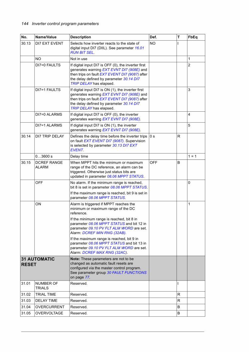
144 Inverter control program parameters
30.13 DI7 EXT EVENT Selects how inverter reacts to the state of digital input DI7 (DIIL). See parameter 16.01 RUN BIT SEL.
NO I
NO Not in use 1
DI7=0 FAULTS If digital input DI7 is OFF (0), the inverter first generates warning EXT EVNT DI7 (908E) and then trips on fault EXT EVENT DI7 (9087) after the delay defined by parameter 30.14 DI7 TRIP DELAY has elapsed.
2
DI7=1 FAULTS If digital input DI7 is ON (1), the inverter first generates warning EXT EVNT DI7 (908E) and then trips on fault EXT EVENT DI7 (9087) after the delay defined by parameter 30.14 DI7 TRIP DELAY has elapsed.
3
DI7=0 ALARMS If digital input DI7 is OFF (0), the inverter generates warning EXT EVNT DI7 (908E).
4
DI7=1 ALARMS If digital input DI7 is ON (1), the inverter generates warning EXT EVNT DI7 (908E).
5
30.14 DI7 TRIP DELAY Defines the delay time before the inverter trips on fault EXT EVENT DI7 (9087). Supervision is selected by parameter 30.13 DI7 EXT EVENT.
0 s R
0…3600 s Delay time 1 = 1
30.15 DCREF RANGE ALARM
When MPPT hits the minimum or maximum range of the DC reference, an alarm can be triggered. Otherwise just status bits are updated in parameter 08.06 MPPT STATUS.
OFF B
OFF No alarm. If the minimum range is reached, bit 8 is set in parameter 08.06 MPPT STATUS.
If the maximum range is reached, bit 9 is set in parameter 08.06 MPPT STATUS.
0
ON Alarm is triggered if MPPT reaches the minimum or maximum range of the DC reference.
If the minimum range is reached, bit 8 in parameter 08.06 MPPT STATUS and bit 12 in parameter 09.10 PV FLT ALM WORD are set. Alarm: DCREF MIN RNG (32AB).
If the maximum range is reached, bit 9 in parameter 08.06 MPPT STATUS and bit 13 in parameter 09.10 PV FLT ALM WORD are set. Alarm: DCREF MAX RNG (32AC).
1
31 AUTOMATIC RESET
Note: These parameters are not to be changed as automatic fault resets are configured via the master control program. See parameter group 30 FAULT FUNCTIONS on page 77.
31.01 NUMBER OF TRIALS
Reserved. I
31.02 TRIAL TIME Reserved. R
31.03 DELAY TIME Reserved. R
31.04 OVERCURRENT Reserved. B
31.05 OVERVOLTAGE Reserved. B
No. Name/Value Description Def. T FbEq

Inverter control program parameters 145
31.06 UNDERVOLTAGE Reserved. B
39 MPPT CONTROL Maximum power point tracking (MPPT) settings.
See also section Maximum power point tracking (MPPT) on page 34.
39.01 MPPT CONTROL Enables/disables MPPT. ON B
OFF MPPT disabled. 0
ON MPPT enabled. 1
39.02 MPPT UDC STEP Defines the DC voltage steps that is used by the MPPT logic when seeking the maximum power point.
7 V R
0 … 1249 V DC voltage step. 10 = 1 V
39.04 MPPT DC REF MAX
Maximum DC reference value allowed for MPPT.
Varies R
[39.05] … 850 V Maximum DC reference. 1 = 1 V
39.05 MPPT DC REF MIN Minimum DC reference value allowed for MPPT.
Varies R
Varies … [39.04] V Minimum DC reference. 1 = 1 V
39.06 GRIDMON SUPV MODE
Determines the action when a grid failure is detected by the grid monitoring relay.
NONE I
NONE No action taken. 0
ALARM An alarm is given. 1
FAULT A fault is generated. 2
RESTART An alarm is given, the delay specified by parameter 39.07 GRIDMON RESTR DLY starts. The inverter is restarted after the delay elapses. If the fault still exists, restart is attempted after another delay period. The cycle is repeated until the grid failure is removed.
3
39.07 GRIDMON RESTR DLY
When parameter 39.06 GRIDMON SUPV MODE is set to RESTART, determines the delay before a restart is attempted.
0 ms R
0…8388607 ms Restart delay 1 = 1 ms
39.08 ENA EXT DC REF Enables/disables external DC reference. When enabled, the external reference overrides the internal MPPT reference.
See master control program parameter 23.01 EXT MPPT DC REF (page 72).
OFF B
OFF External DC reference disabled. Internal MPPT reference used.
0
ON External DC reference enabled. The external reference overrides the internal MPPT reference.
1
39.09 EXT MPPT DC REF
Shows the external DC reference. This reference is used when parameter 39.08 ENA EXT DC REF is set to ON.
0 V B
0…1500 External DC reference 1 = 1 V
No. Name/Value Description Def. T FbEq

146 Inverter control program parameters
40 LVRT CONTROL Parameters related to the Low voltage ride-through function. Do not change parameters when the PVS800 is running.
Note: Group 40 is write-protected. It can be write-enabled by giving a password with parameter 16.03 PASS CODE.
40.01 LVRT MODE Voltage tracking source selection for the Low voltage ride-through function.
Selection between phase and main voltages can be set in parameter 40.24 RMS VOLTAGE CALC.
Note: Parameter 40.01 LVRT MODE is write-protected when the PVS800 is running. Stop the PVS800 before changing the value.
Note: Perform the following checks before enabling the LVRT function:
• Check that the mains voltage measurement is OK (signal 01.11 MAINS VOLTAGE).
• Check that the RT area parameters are set correctly, see the figure of parameter 40.10 LVRT U/Un LEVEL 1.
• Check the settings for the grid support mode (parameter 41.01 GRID SUPPORT MODE).
POS SEQ VOLT
I
OFF LVRT function is disabled. 0
MAX RMS VOLT Input for the LVRT function is the highest RMS AC voltage, either phase or main.
1
MIN RMS VOLT Input for the LVRT function is the lowest RMS AC voltage, either phase or main.
2
POS SEQ VOLT Input for the LVRT function is the positive sequence of the AC voltage.
3
40.03 LVRT RETURN RAMP
Defines a ramping time for active power after a voltage dip. When the grid voltage has returned to a normal value after the voltage dip, the active power is restored using this ramp time.
3 s R
0…100 s Ramp time 10 = 1 s
40.09 RT U/Un MOD STOP
Modulation stops if the value of 01.11 MAINS VOLTAGE falls below the value of this parameter. Check the RT area parameters. See the figure at parameter 40.10 LVRT U/Un LEVEL 1.
0% R
0…90% Modulation stop limit of the RT function 1 = 1%
No. Name/Value Description Def. T FbEq

Inverter control program parameters 147
40.10 LVRT U/Un LEVEL 1
Defines the trigger level for the LVRT function. See the figure below for information on defining the allowed LVRT area.
After the LVRT function is triggered, bit 11 of 08.01 MAIN STATUS WORD is set and an alarm (LVRT RIDETRGH (32A0)) is generated.
If the grid voltage falls to the inverter trip area, the inverter unit will trip on RT NET LOST (32A1).
80% R
[40.11]…200% Level 1 1 = 1%
40.11 LVRT U/Un LEVEL 2
LVRT voltage level 2. See the figure in parameter 41.10 LVRT U/Un LEVEL 1.
0% R
0…[40.10]% Level 2 1 = 1%
40.12 LVRT U/Un LEVEL 3
LVRT voltage level 3. See the figure in parameter 40.10 LVRT U/Un LEVEL 1.
20% R
[40.11]…200% Level 3 1 = 1%
40.13 LVRT DELTA t1 Defines the time (t1) within which 01.11 MAINS VOLTAGE should be restored above 40.25 LVRT U/Un LEVEL 4.
1000 ms R
[40.14]…[40.15] ms Time 1 1 = 1 ms
40.14 LVRT DELTA t2 Defines the time (t2) within which 01.11 MAINS VOLTAGE should be restored above 40.12 LVRT U/Un LEVEL 3.
600 ms R
0…[40.13] ms Time 2 1 = 1 ms
40.15 LVRT DELTA t3 Defines the time (t3) within which 01.11 MAINS VOLTAGE should be restored above 40.26 LVRT U/Un LEVEL 5.
1500 ms R
[40.13]…[40.16] ms Time 3 1 = 1 ms
No. Name/Value Description Def. T FbEq
Inverter trip area
U/UN
t
40.10 LVRT U/Un LEVEL 1 40.28 LVRT U/Un END
40.12 LVRT U/Un LEVEL 3
40.27 LVRT U/Un LEVEL 6
40.26 LVRT U/Un LEVEL 5
40.25 LVRT U/Un LEVEL 4
40.11 LVRT U/Un LEVEL 2
40.14 LVRT DELTA t2
40.13 LVRT DELTA t1
40.15 LVRT DELTA t3
40.16 LVRT DELTA t4
40.17 LVRT DELTA t5

148 Inverter control program parameters
40.16 LVRT DELTA t4 Defines the time (t4) within which 01.11 MAINS VOLTAGE should be restored above 40.27 LVRT U/Un LEVEL 6.
2000 ms R
[40.15]…[40.17] ms Time 4 1 = 1 ms
40.17 LVRT DELTA t5 Defines the time (t5) within which 01.11 MAINS VOLTAGE must be restored above 40.28 LVRT U/Un END.
3000 ms R
[40.16]…8388608 ms
Time 5 1 = 1 ms
40.24 RMS VOLTAGE CALC
Enables/disables RMS voltage measuring. MAIN VOLT I
OFF RMS voltage measuring is disabled. 0
PHASE VOLT RMS phase voltage measuring is enabled. 1
MAIN VOLT RMS main voltage measuring is enabled. 2
40.25 LVRT U/Un LEVEL 4
LVRT voltage level 4. See the figure in parameter 40.10 LVRT U/Un LEVEL 1.
45% R
[40.12]…200% Level 4 1 = 1%
40.26 LVRT U/Un LEVEL 5
LVRT voltage level 5. See the figure in parameter 40.10 LVRT U/Un LEVEL 1.
60% R
[40.25]…200% Level 5 1 = 1%
40.27 LVRT U/Un LEVEL 6
LVRT voltage level 6. See the figure in parameter 40.10 LVRT U/Un LEVEL 1.
75% R
[40.26]…200% Level 6 1 = 1%
40.28 LVRT U/Un END End level for LVRT. See the figure in parameter 40.10 LVRT U/Un LEVEL 1.
85% R
[40.10]…200% End level 1 = 1%
41 GRID SUPPORT Parameters related to the Grid support function.
Note: Group 41 is write-protected. It can be write-enabled by giving a password with parameter 16.03 PASS CODE. Parameter 41.01 GRID SUPPORT MODE is write-protected when the PVS800 is running.
41.01 GRID SUPPORT MODE
Selects the operation mode of the Grid support function. Grid support means feeding of capacitive reactive power to the grid upon voltage dip (ie, when bit 11 of 08.01 MAIN STATUS WORD is set). The amount of grid support is defined by parameters 41.03…41.10.
Selection between phase and main voltages can be set in parameter 40.24 RMS VOLTAGE CALC.
OFF I
OFF Grid support function is disabled. 0
MAX RMS VOLT Input for the grid support function is the highest RMS AC voltage, either phase or main.
1
MIN RMS VOLT Input for the grid support function is the lowest RMS AC voltage, either phase or main.
2
POS SEQ VOLT Input for the grid support function is a positive sequence of the AC voltage.
3
No. Name/Value Description Def. T FbEq

Inverter control program parameters 149
41.03 GS U/Un LEVEL 1 Defines grid support level 1. When the voltage falls below this level, the grid is supported by feeding capacitive current as defined by 41.07 GS IQREF LEVEL 1.
100% R
[41.04]…200% Grid support voltage level 1 1 = 1%
41.04 GS U/Un LEVEL 2 Defines grid support level 2. When the voltage falls below this level, the grid is supported by feeding capacitive current as defined by 41.08 GS IQREF LEVEL 2.
50% R
[41.05]…[41.03]% Grid support voltage level 2 1 = 1%
41.05 GS U/Un LEVEL 3 Defines grid support level 3. When the voltage falls below this level, the grid is supported by feeding capacitive current as defined by 41.09 GS IQREF LEVEL 3.
25% R
[41.06]…[41.04]% Grid support voltage level 3 1 = 1%
41.06 GS U/Un LEVEL 4 Defines grid support level 4. When the voltage falls below this level, the grid is supported by feeding capacitive current as defined by 41.10 GS IQREF LEVEL 4.
15% R
0…[41.05]% Grid support voltage level 4 1 = 1%
41.07 GS IQREF LEVEL 1
Defines the reactive current reference point for 41.03 GS U/Un LEVEL 1 in percent of 04.05 NOM AC CURRENT.
0% R
0…100% Grid support reference level 1 1 = 1%
41.08 GS IQREF LEVEL 2
Defines the reactive current reference point for 41.04 GS U/Un LEVEL 2 in percent of 04.05 04.05 NOM AC CURRENT.
100% R
0…100% Grid support reference level 2 1 = 1%
No. Name/Value Description Def. T FbEq
IQ,ref
41.10 GS IQREF LEVEL 4
41.09 GS IQREF LEVEL 3
41.08 GS IQREF LEVEL 2
41.07 GS IQREF LEVEL 1
41.06 GS U/Un LEVEL 4
41.05 GS U/Un LEVEL 3
41.04 GS U/Un LEVEL 2 41.19 GS U/Un LEVEL 5
0 %
41.22 GS IQREF LEVEL 5
41.23 GS IQREF LEVEL 6
41.24 GS IQREF LEVEL 7
41.03 GS U/Un LEVEL 1 41.20 GS U/Un LEVEL 6
41.21 GS U/Un LEVEL 7
U/UN
UNDER VOLTAGE OVERVOLTAGE
100 %

150 Inverter control program parameters
41.09 GS IQREF LEVEL 3
Defines the reactive current reference point for 41.05 GS U/Un LEVEL 3 in percent of 04.05 NOM AC CURRENT.
100% R
0…100% Grid support reference level 3 1 = 1%
41.10 GS IQREF LEVEL 4
Defines the reactive current reference point for 41.06 GS U/Un LEVEL 4 in percent of 04.05 NOM AC CURRENT.
100% R
0…100% Grid support reference level 4 1 = 1%
41.11 RT IQREF Defines an external reactive current reference during a voltage dip. If the value differs from 0, the reactive current reference defined by parameters 41.03…40.10 is bypassed.
Value is given as a percentage of parameter 04.05 NOM AC CURRENT.
0% R
0…100% Reactive current reference 1 = 1%
41.12 RT IQ RAMP UP Defines the ramp time from zero to nominal current (04.05 NOM AC CURRENT) for the reactive current reference.
Ramp time is used if parameter 40.01 LVRT MODE is activated and the voltage dip is active.
0.04 s R
0…100 s Ramp time 10 = 1 s
41.14 GS UAC REF SEL Defines a reference level of the AC voltage for the low voltage grid support calculation.
NOMINAL VOLT
NOMINAL VOLT Parameter 04.04 NOM AC VOLTAGE is used as reference. Grid support is calculated with the difference between actual voltage and value in parameter 04.04 NOM AC VOLTAGE. This result is also used as input for grid support curve (parameters 41.03 GS U/Un LEVEL 1...41.10 GS IQREF LEVEL 4).
0
60 s AVERAGE Parameter 02.08 60 s AVERAGE VOLT is used as reference. Grid support is calculated with the difference between actual voltage and value in parameter 02.08 60 s AVERAGE VOLT. This result is also used as input for grid support curve (parameters 41.03 GS U/Un LEVEL 1...41.10 GS IQREF LEVEL 4).
1
41.15 GS TURN OFF TIME
Defines the turn off time for grid support after a voltage dip. The grid support stays on for this delay time after the voltage dip ends.
0 ms
0...8388610 ms Delay time 1 = 1 ms
41.16 GS IQREF BASE SEL
Defines the base value of reactive current reference which is used with the low voltage grid support.
ZERO
ZERO When the low voltage ride-through is active, the existing reactive current reference is ignored. Reactive current reference comes only from the grid support curve (parameters 41.03…40.10).
0
60 s AVERAGE Reactive current reference calculated from the grid support curve (parameters 41.03…40.10) is added to parameter 02.04 60 s AVERAGE IQ during the low voltage ride-through.
1
No. Name/Value Description Def. T FbEq

Inverter control program parameters 151
41.17 HV GS IQREF BASE
Defines the base value of reactive current reference which is used with the high voltage grid support.
IQ REF
ZERO When the high voltage ride-through is active, the existing reactive current reference is ignored. Reactive current reference comes only from the grid support curve (parameters 41.19…41.24).
0
IQ REF Reactive current reference calculated from the grid support curve (parameters 41.19…41.24) is added to the existing reactive current reference.
1
41.18 HV GS MODE Defines an input mode for the High voltage ride-through (HVRT) function.
OFF
OFF HVRT is not used. 0
MAX RMS VOLT HVRT is based on the maximum value of the calculated RMS voltages.
1
MIN RMS VOLT HVRT is based on the minimum value of the calculated RMS voltages.
2
POS SEQ VOLT HVRT is based on the positive sequence component of the grid voltage.
3
41.19 GS U/Un LEVEL 5 Defines the voltage at the 5th point of the grid support curve.
110%
100% … [41.20] 1 = 1%
41.20 GS U/Un LEVEL 6 Defines the voltage at the 6th point of the grid support curve.
120%
[41.19]…[41.21] 1 = 1%
41.21 GS U/Un LEVEL 7 Defines the voltage at the 7th point of the grid support curve.
120%
[41.20] … 200% 1 = 1%
41.22 GS IQREF LEVEL 5
Defines the active current reference at the 5th point of the grid support curve.
0%
-100…0% Reactive current reference in percent of 04.05 NOM AC CURRENT.
1 = 1%
41.23 GS IQREF LEVEL 6
Defines the active current reference at the 6th point of the grid support curve.
-30%
-100…0% Reactive current reference in percent of 04.05 NOM AC CURRENT.
1 = 1%
41.24 GS IQREF LEVEL 7
Defines the active current reference at the 7th point of the grid support curve.
-30%
-100…0% Reactive current reference in percent of 04.05 NOM AC CURRENT.
1 = 1%
41.25 UNBALANCE LEVEL
Defines a level to detect unbalanced voltage dip. The unbalanced dip is detected when the ratio of negative sequence voltage (parameter 02.10 NEG SEQUENCE VOLT) to the positive sequence voltage (parameter 01.11 MAINS VOLTAGE) is greater than the level defined in this parameter.
If the unbalanced dip is detected, the reactive current is limited to a value set in the parameter 41.25 UNBALANCE LEVEL
100%
0…100% Unbalance level 1 = 1%
No. Name/Value Description Def. T FbEq
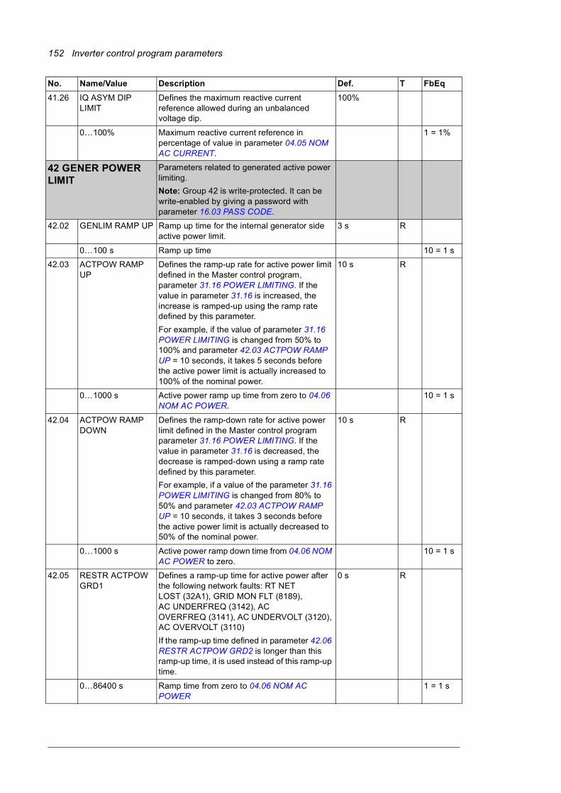
152 Inverter control program parameters
41.26 IQ ASYM DIP LIMIT
Defines the maximum reactive current reference allowed during an unbalanced voltage dip.
100%
0…100% Maximum reactive current reference in percentage of value in parameter 04.05 NOM AC CURRENT.
1 = 1%
42 GENER POWER LIMIT
Parameters related to generated active power limiting.
Note: Group 42 is write-protected. It can be write-enabled by giving a password with parameter 16.03 PASS CODE.
42.02 GENLIM RAMP UP Ramp up time for the internal generator side active power limit.
3 s R
0…100 s Ramp up time 10 = 1 s
42.03 ACTPOW RAMP UP
Defines the ramp-up rate for active power limit defined in the Master control program, parameter 31.16 POWER LIMITING. If the value in parameter 31.16 is increased, the increase is ramped-up using the ramp rate defined by this parameter.
For example, if the value of parameter 31.16 POWER LIMITING is changed from 50% to 100% and parameter 42.03 ACTPOW RAMP UP = 10 seconds, it takes 5 seconds before the active power limit is actually increased to 100% of the nominal power.
10 s R
0…1000 s Active power ramp up time from zero to 04.06 NOM AC POWER.
10 = 1 s
42.04 ACTPOW RAMP DOWN
Defines the ramp-down rate for active power limit defined in the Master control program parameter 31.16 POWER LIMITING. If the value in parameter 31.16 is decreased, the decrease is ramped-down using a ramp rate defined by this parameter.
For example, if a value of the parameter 31.16 POWER LIMITING is changed from 80% to 50% and parameter 42.03 ACTPOW RAMP UP = 10 seconds, it takes 3 seconds before the active power limit is actually decreased to 50% of the nominal power.
10 s R
0…1000 s Active power ramp down time from 04.06 NOM AC POWER to zero.
10 = 1 s
42.05 RESTR ACTPOW GRD1
Defines a ramp-up time for active power after the following network faults: RT NET LOST (32A1), GRID MON FLT (8189), AC UNDERFREQ (3142), AC OVERFREQ (3141), AC UNDERVOLT (3120), AC OVERVOLT (3110)
If the ramp-up time defined in parameter 42.06 RESTR ACTPOW GRD2 is longer than this ramp-up time, it is used instead of this ramp-up time.
0 s R
0…86400 s Ramp time from zero to 04.06 NOM AC POWER
1 = 1 s
No. Name/Value Description Def. T FbEq

Inverter control program parameters 153
42.06 RESTR ACTPOW GRD2
Defines a ramp-up time for active power after the start-up. This ramp is used after every start of the inverter.
In addition, if this ramp-up time is longer than the ramp-up time in parameter 42.05 RESTR ACTPOW GRD1, this ramp-up time is used instead of 42.05 after a network fault listed in 42.05 has occurred.
0 s R
0…86400 s Ramp time from zero to 04.06 NOM AC POWER
1 = 1 s
42.07 P FREQ LIM ENA Selects the mode of the Active power limitation from grid overfrequency function. Active power is limited according to the limitation curve defined by parameters 42.08 P LIMITING FREQ 1 … 42.11 P LIMITING FREQ 3.
See section Active power limitation from grid overfrequency on page 38.
OFF I
OFF Active power limitation from grid overfrequency is not used.
0
INCREMENTAL Active power limit decreases according to the limitation curve, but increases only when the grid frequency is below 42.11 P LIMITING FREQ 3 longer than 42.13 P(f) RETURN DELAY. Increasing the power limit is done with a ramp rate defined by parameter 42.14 P(f) RETURN RAMP.
1
FREE RUNNING Active power limit can move back and forth within the limitation curve defined by parameters 42.08 P LIMITING FREQ 1 … 42.10 P FREQ LIMIT 2. After the grid frequency is restored below 42.08 P LIMITING FREQ 1, the power limit is increased with a ramp rate defined by parameter 42.14 P(f) RETURN RAMP.
2
42.08 P LIMITING FREQ 1
Defines the grid frequency where the active power limitation curve starts.
50.2 Hz R
[41.11]…[41.09] Start frequency for active power limitation from grid overfrequency
100 = 1 Hz
42.09 P LIMITING FREQ 2
Defines the grid frequency where the active power limitation curve ends. If the grid frequency exceeds this value, the active power is limited to zero.
51.5 Hz R
[41.08]…65 Hz Stop frequency for active power limitation from grid overfrequency
100 = 1 Hz
42.10 P FREQ LIMIT 2 Defines the active power limitation at the frequency defined by parameter 42.09 P LIMITING FREQ 2. The value is given as a percentage of the active power level before limitation.
48% R
0…100% Active power limitation 100 = 1%
No. Name/Value Description Def. T FbEq

154 Inverter control program parameters
42.11 P LIMITING FREQ 3
Defines the frequency where the active power limitation from grid frequency is deactivated. If the frequency-dependent active power limitation is effective (bit 8 in parameter 08.03 LIMIT WORD is set), it is deactivated only when 02.18 GRID FREQUENCY falls below 42.11 P LIMITING FREQ 3.
50.05 R
45…[42.09] Deactivation frequency for active power limitation from grid overfrequency
100 = 1 Hz
42.12 POWER PRIORITY Defines the prioritized power type. If the AC current limit of the inverter is reached, the non-prioritized power type is reduced to keep the AC current below the limit.
ACTIVE POW I
REACTIVE POW Reactive power is prioritized and the active power is limited.
0
ACTIVE POW Active power is prioritized and the reactive current reference is limited.
1
42.13 P(f) RETURN DELAY
Defines a return delay for the active power limitation from grid overfrequency in the incremental mode. For the power limitation to end, the actual grid frequency must be less than 42.11 P LIMITING FREQ 3 for a time period longer than this delay.
The delay is active only if parameter 42.07 P FREQ LIM ENA is set to INCREMENTAL.
0 s R
0…419430 s Return delay 20 = 1 s
42.14 P(f) RETURN RAMP
Defines a ramp time for active power recovery after the active power limitation from grid overfrequency has ended. Time means ramping from zero to nominal power.
The ramp is used if parameter 42.07 P FREQ LIM ENA is set to INCREMENTAL or FREE RUNNING.
300 s R
0…419430 s Ramp time 20 = 1 s
42.15 P(f) RET RAMP MAX
Defines the maximum ramping time from zero to nominal power when the inverter is returning from the grid overfrequency transient.
The ramp selections MEMORY and DELTA in parameter 42.16 P(f) RET RAMP SEL may lead to very slow return ramps. Parameter 42.15 can be used to set a reasonable maximum ramping time.
1200 s R 20 = 1 s
1…1200 s Maximum ramping time
42.16 P(f) RET RAMP SEL
Selects which power the return ramp time in parameter 42.14 P(f) RETURN RAMP refers to.
NOMINAL
NOMINAL Return ramp time in parameter 42.14 P(F) RETURN RAMP means ramping from zero to nominal power (04.06 NOM AC POWER).
0
MEMORY Return ramp time in parameter 42.14 P(F) RETURN RAMP means ramping from zero power to Pe-mem, where
• Pe-mem = Active power level when the
overfrequency transient was started.
1
No. Name/Value Description Def. T FbEq
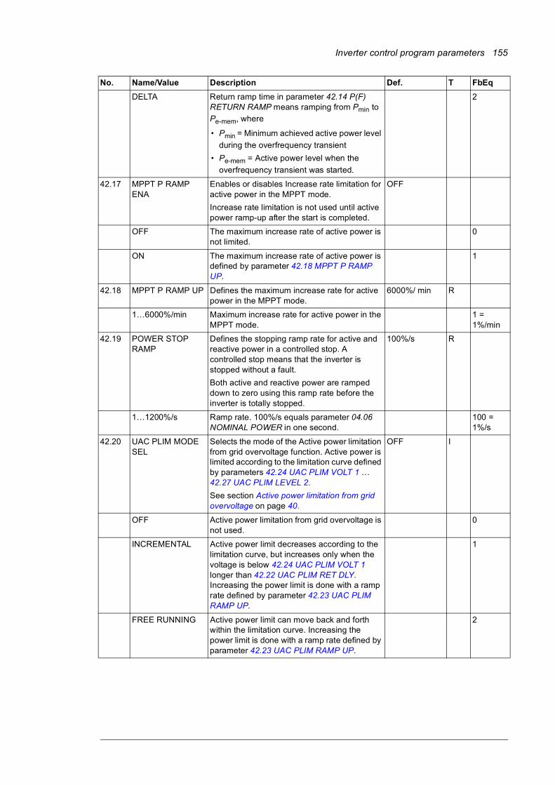
Inverter control program parameters 155
DELTA Return ramp time in parameter 42.14 P(F) RETURN RAMP means ramping from Pmin to
Pe-mem, where
• Pmin = Minimum achieved active power level
during the overfrequency transient
• Pe-mem = Active power level when the
overfrequency transient was started.
2
42.17 MPPT P RAMP ENA
Enables or disables Increase rate limitation for active power in the MPPT mode.
Increase rate limitation is not used until active power ramp-up after the start is completed.
OFF
OFF The maximum increase rate of active power is not limited.
0
ON The maximum increase rate of active power is defined by parameter 42.18 MPPT P RAMP UP.
1
42.18 MPPT P RAMP UP Defines the maximum increase rate for active power in the MPPT mode.
6000%/ min R
1…6000%/min Maximum increase rate for active power in the MPPT mode.
1 = 1%/min
42.19 POWER STOP RAMP
Defines the stopping ramp rate for active and reactive power in a controlled stop. A controlled stop means that the inverter is stopped without a fault.
Both active and reactive power are ramped down to zero using this ramp rate before the inverter is totally stopped.
100%/s R
1…1200%/s Ramp rate. 100%/s equals parameter 04.06 NOMINAL POWER in one second.
100 = 1%/s
42.20 UAC PLIM MODE SEL
Selects the mode of the Active power limitation from grid overvoltage function. Active power is limited according to the limitation curve defined by parameters 42.24 UAC PLIM VOLT 1 … 42.27 UAC PLIM LEVEL 2.
See section Active power limitation from grid overvoltage on page 40.
OFF I
OFF Active power limitation from grid overvoltage is not used.
0
INCREMENTAL Active power limit decreases according to the limitation curve, but increases only when the voltage is below 42.24 UAC PLIM VOLT 1 longer than 42.22 UAC PLIM RET DLY. Increasing the power limit is done with a ramp rate defined by parameter 42.23 UAC PLIM RAMP UP.
1
FREE RUNNING Active power limit can move back and forth within the limitation curve. Increasing the power limit is done with a ramp rate defined by parameter 42.23 UAC PLIM RAMP UP.
2
No. Name/Value Description Def. T FbEq

156 Inverter control program parameters
42.21 UAC PLIM INPUT Selects the input for the active power limitation from grid overvoltage.
POS SEQ
VOLT
I
POS SEQ VOLT Active power limitation from the positive sequence of the AC voltage (01.11 MAINS VOLTAGE).
0
10-MIN AVG Active power limitation from the 10-minute moving average of the AC voltage (02.09 AVERAGE AC VOLT).
1
42.22 UAC PLIM RET DLY
Defines a return delay for the active power limitation from grid overvoltage in the incremental mode. Grid voltage must be below 42.24 UAC PLIM VOLT 1 longer than this delay before the active power limit can be increased again.
This setting is used only if parameter 42.20 UAC PLIM MODE SEL is set to INCREMENTAL.
300 s R
0…10000 s Return delay 20 = 1 s
42.23 UAC PLIM RAMP UP
Defines a ramp rate for the active power limitation from grid overvoltage. The active power limit is always increased with this ramp rate.
20 %/min R
1…6000 %/min Ramp rate 1 = 1 %/min
42.24 UAC PLIM VOLT 1 Defines a voltage value for the first point in the active power limitation curve.
105% R
100…[42.26] V Voltage in percent of 04.04 NOM AC VOLTAGE
10 = 1%
42.25 UAC PLIM LEVEL 1
Defines an active power level for the first point in the active power limitation curve.
100% R
[42.27]…120 % Active power level in percent of 04.06 NOM AC POWER
100 = 1%
42.26 UAC PLIM VOLT 2 Defines a voltage value for the second point in the active power limitation curve.
110% R
[42.24]…150 % Voltage in percent of 04.04 NOM AC VOLTAGE
10 = 1%
42.27 UAC PLIM LEVEL 2
Defines an active power level for the second point in the active power limitation curve.
0% R
0…[42.25] % Active power level in percent of 04.06 NOM AC POWER
100 = 1%
44 GRID MONITORING
Parameters related to internal grid monitoring.
Note: Group 44 is write-protected. It can be write-enabled by giving a password with parameter 16.03 PASS CODE.
44.01 NAMU GRIDMON MODE
Defines the usage mode of the internal grid monitoring. Grid monitoring is based on the voltage measurement via the NAMU board.
FAULT I
NONE Internal grid monitoring is disabled. 0
ALARM Internal grid monitoring is enabled. If grid voltage and/or frequency are outside limits that are defined by parameters 44.02…44.17, a corresponding alarm is created and the inverter continues to operate.
1
No. Name/Value Description Def. T FbEq

Inverter control program parameters 157
FAULT Internal grid monitoring is enabled. If grid voltage and/or frequency are outside limits that are defined by parameters 44.02…44.17, a corresponding fault is created and the inverter stops.
2
44.02 UNDER FREQ 1 LIM
Defines a trip limit for under frequency fault 1. If the grid frequency (signal 02.18 GRID FREQUENCY) is below this setting longer than the time delay in parameter 44.04 UNDER FREQ 1 TIME, the inverter will generate an alarm or a fault according to parameter 44.01 NAMU GRIDMON MODE.
47.5 Hz R
45…65 Hz Trip limit 1 100 = 1 Hz
44.03 UNDER FREQ 2 LIM
Defines a trip limit for under frequency fault 2. If the grid frequency (signal 02.18 GRID FREQUENCY) is below this setting longer than the time delay in parameter 44.05 UNDER FREQ 2 TIME, the inverter will generate an alarm or a fault according to parameter 44.01 NAMU GRIDMON MODE.
47.5 Hz R
45…65 Hz Trip limit 2 100 = 1 Hz
44.04 UNDER FREQ 1 TIME
Defines a trip time for under frequency fault 1. 0.1 s R
0…33554.4 s Trip time 1 100 = 1 s
44.05 UNDER FREQ 2 TIME
Defines a trip time for under frequency fault 2. 0.1 s R
0…33554.4 s Trip time 2 100 = 1 s
44.06 OVER FREQ 1 LIM Defines a trip limit for over frequency fault 1. If the grid frequency (signal 02.18 GRID FREQUENCY) exceeds this setting longer than the time delay in parameter 44.08 OVER FREQ 1 TIME, the inverter will generate an alarm or a fault according to parameter 44.01 NAMU GRIDMON MODE.
51.5 Hz R
45…65 Hz Trip limit 1 100 = 1 Hz
44.07 OVER FREQ 2 LIM Defines a trip limit for over frequency fault 2. If the grid frequency (signal 02.18 GRID FREQUENCY) exceeds this setting longer than the time delay in parameter 44.09 OVER FREQ 2 TIME, the inverter will generate an alarm or a fault according to parameter 44.01 NAMU GRIDMON MODE.
51.5 Hz R
45…65 Hz Trip limit 2 100 = 1 Hz
44.08 OVER FREQ 1 TIME
Defines a trip time for over frequency fault 1. 0.1 s R
0…33554.4 s Trip time 1 100 = 1 s
44.09 OVER FREQ 2 TIME
Defines a trip time for over frequency fault 2. 0.1 s R
0…33554.4 s Trip time 2 100 = 1 s
No. Name/Value Description Def. T FbEq

158 Inverter control program parameters
44.10 UNDER VOLT 1 LIM
Defines a trip limit for under voltage fault 1. If the grid voltage (signal 01.11 MAINS VOLTAGE) is below this setting longer than the time delay in parameter 44.12 UNDER VOLT 1 TIME, the inverter will generate an alarm or a fault according to parameter 44.01 NAMU GRIDMON MODE.
80% R
0…200% Trip limit 1 1 = 1%
44.11 UNDER VOLT 2 LIM
Defines a trip limit for under voltage fault 2. If the grid voltage (signal 01.11 MAINS VOLTAGE) is below this setting longer than the time delay in parameter 44.13 UNDER VOLT 2 TIME, the inverter will generate an alarm or a fault according to parameter 44.01 NAMU GRIDMON MODE.
80% R
0…200% Trip limit 2 1 = 1%
44.12 UNDER VOLT 1 TIME
Defines a trip time for under voltage fault 1. 1.5 s R
0…33554.4 s Trip time 1 100 = 1 s
44.13 UNDER VOLT 2 TIME
Defines a trip time for under voltage fault 2. 1.5 s R
0…33554.4 s Trip time 2 100 = 1 s
44.14 OVER VOLT 1 LIM Defines a trip limit for over voltage fault 1. If the grid voltage (signal 01.11 MAINS VOLTAGE) exceeds this setting longer than the time delay in parameter 44.16 OVER VOLT 1 TIME, the inverter will generate an alarm or a fault according to parameter 44.01 NAMU GRIDMON MODE.
120% R
0…200% Trip limit 1 1 = 1%
44.15 OVER VOLT 2 LIM Defines a trip limit for over voltage fault 2. If the grid voltage (signal 01.11 MAINS VOLTAGE) exceeds this setting longer than the time delay in parameter 44.17 OVER VOLT 2 TIME, the inverter will generate an alarm or a fault according to parameter 44.01 NAMU GRIDMON MODE.
120% R
0…200% Trip limit 2 1 = 1%
44.16 OVER VOLT 1 TIME
Defines a trip time for over voltage fault 1. 0.1 s R
0…33554.4 s Trip time 1 100 = 1 s
44.17 OVER VOLT 2 TIME
Defines a trip time for over voltage fault 2. 0.1 s R
0…33554.4 s Trip time 2 100 = 1 s
No. Name/Value Description Def. T FbEq

Inverter control program parameters 159
44.18 CUT-IN CHECK ENA
Enables or disables the checking of cut-in conditions (start conditions). Cut-in condition checking is based on measurements from the NAMU board.
The limits for cut-in conditions are defined by parameters 44.19 CUT-IN FREQ LOW … 44.22 CUT-IN VOLT HIGH. See the figure below for more information.
ON B
OFF Checking of cut-in conditions is disabled. 0
ON Checking of cut-in conditions is enabled. 1
44.19 CUT-IN FREQ LOW
Defines the low limit for the frequency cut-in condition.
47.5 Hz R
45…65 Hz Low limit for the grid frequency 100 = 1 Hz
44.20 CUT-IN FREQ HIGH
Defines the high limit for the frequency cut-in condition.
50.05 Hz R
45…65 Hz High limit for the grid frequency 100 = 1 Hz
44.21 CUT-IN VOLT LOW Defines the low limit for the voltage cut-in condition.
90% R
90…110% Low limit for the grid voltage 1 = 1%
44.22 CUT-IN VOLT HIGH
Defines the high limit for the voltage cut-in condition.
110% R
90…110% High limit for the grid voltage 1 = 1%
44.23 CUT-IN DELAY Defines the delay for the checking of cut-in conditions. Grid frequency and grid voltage have to be within the limits defined by parameters 44.19 CUT-IN FREQ LOW … 44.22 CUT-IN VOLT HIGH longer than this delay before the inverter can be started.
0 s R
0… 419430 s Time delay for the checking of cut-in conditions 20 = 1 s
44.24 GRIDMON INPUT
SEL
Selects the input for grid voltage monitoring. POS SEQ VOLT
POS SEQ VOLT Grid monitoring for undervoltage and overvoltage is based on the positive sequence component of the grid voltage.
0
No. Name/Value Description Def. T FbEq
44.19 CUT-IN FREQ LOW
02.18 GRID FREQUENCY
01.11 MAINS VOLTAGE
Region where PVS800 can be started
44.22 CUT-IN VOLT HIGHUN(AC)44.21 CUT-IN VOLT LOW
50/60 Hz
44.20 CUT-IN FREQ HIGH

160 Inverter control program parameters
RMS VOLT Undervoltage detection is based on the minimum RMS value and overvoltage detection on the maximum RMS value of the grid voltage.
The selection between phase-to-neutral and phase-to-phase voltages is done with parameter 40.24 RMS VOLTAGE CALC.
1
45 ANTI-ISLANDING Parameters related to island detection.
Note: Group 45 is write-protected. It can be write-enabled by giving a password with parameter 16.03 PASS CODE.
45.01 ISLAND DETECTION
Selects the operation mode of the island detection.
NONE I
NONE Island detection is disabled. 0
FAULT Island detection is enabled. When an island is detected, the inverter trips on a fault.
1
RESTART Island detection is enabled. When an island is detected, the inverter is stopped and an alarm generated. The inverter starts again after the delay defined by parameter 45.06 ANTI-ISLAND DELAY.
Note: If the delay is short (less than 30 seconds), the Low voltage ride-through (LVRT) function is needed for a fast start.
2
45.02 ANTI-ISLAND MODE
Defines the method of the Anti-islanding function.
PASSIVE I
PASSIVE Passive anti-islanding. The inverter does not do any action for island detection.
1
RPV Active anti-islanding (reactive power variation). The reactive power variation makes a cyclic reactive power excitation to detect the island.
2
FREQ SHIFT Active anti-islanding (by frequency shift). The grid frequency is shifted out of its normal range by utilizing positive feedback from the grid frequency.
3
45.03 RPV CYCLE TIME Defines the cycle time of the additional reactive power reference in the reactive power variation (RPV) method.
1 s R
0…8388.61 s RPV cycle time 1000 = 1 s
45.04 RPV AMPLITUDE Amplitude of the reactive power reference in the RPV method. Amplitude is defined in percentage of the parameter 04.06 NOM AC POWER when the inverter is running with full active power.
Actual used amplitude of the used reactive power reference is scaled according to the present active power level.
1% R
0…100% Amplitude of the reactive power reference in percent of 04.06 NOM AC POWER.
100 = 1%
45.05 ROCOF PEAK TRIP
Defines a trip level for the grid frequency change rate (ROCOF, rate of change of frequency).
4 Hz/s R
0…390.625 Hz/s Trip level for the grid frequency change rate 100 = 1 Hz/s
No. Name/Value Description Def. T FbEq

Inverter control program parameters 161
45.06 ANTI-ISLAND DELAY
Defines a delay for the anti-islanding restart mode. When an island is detected, the inverter is disconnected from the grid and alarm ANTI-ISLAND (81A0) is generated. The inverter starts again after the delay, provided that there are no faults active.
Note: If the delay is short (less than 30 seconds), the Low voltage ride-through (LVRT) function is needed for a fast start.
5 s R
0…8388.61 s Time delay for the anti-islanding restart mode 1000 = 1 s
45.07 ROCOF CONST LEVEL
Defines a constant ROCOF level for the island detection. The island is detected when the grid frequency change rate (ROCOF) is beyond this level for the time delay defined in parameter 45.08 ROCOF CONST DELAY.
The constant ROCOF level detection is enabled only when parameter 45.11 CONST DETECTION = ON.
The island detected by the constant level detection is indicated with bit 7, in parameter 08.08 ISLAND STATUS.
2 Hz/s
0…390.625 Hz/s Detection level. 100 = 1 Hz/s
45.08 ROCOF CONST DELAY
Defines the time delay for constant level island detection. The island is detected when grid frequency change rate (ROCOF) is beyond the level defined in parameter 45.07 ROCOF CONST LEVEL for the delay defined in this parameter.
0.2 s
0…8388.61 s Detection delay. 1000 = 1 s
45.09 PEAK DETECTION Activates island detection from peak ROCOF value.
ON
OFF Peak detection is disabled 0
ON Peak detection is enabled 1
45.10 ADAPT DETECTION
Activates island detection from adaptive ROCOF value.
ON
OFF Adapt detection is disabled 0
ON Adapt detection is enabled 1
45.11 CONST DETECTION
Activates island detection from constant ROCOF value with delay.
ON
OFF Constant detection is disabled 0
ON Constant detection is enabled 1
45.12 FREQ SHIFT GAIN Defines gain for frequency shift algorithm. Gain affects the strength of positive feedback. A too large gain can cause instability in the system.
100%/Hz
10...200%/Hz Frequency shift gain 1 = 1%/HZ
No. Name/Value Description Def. T FbEq
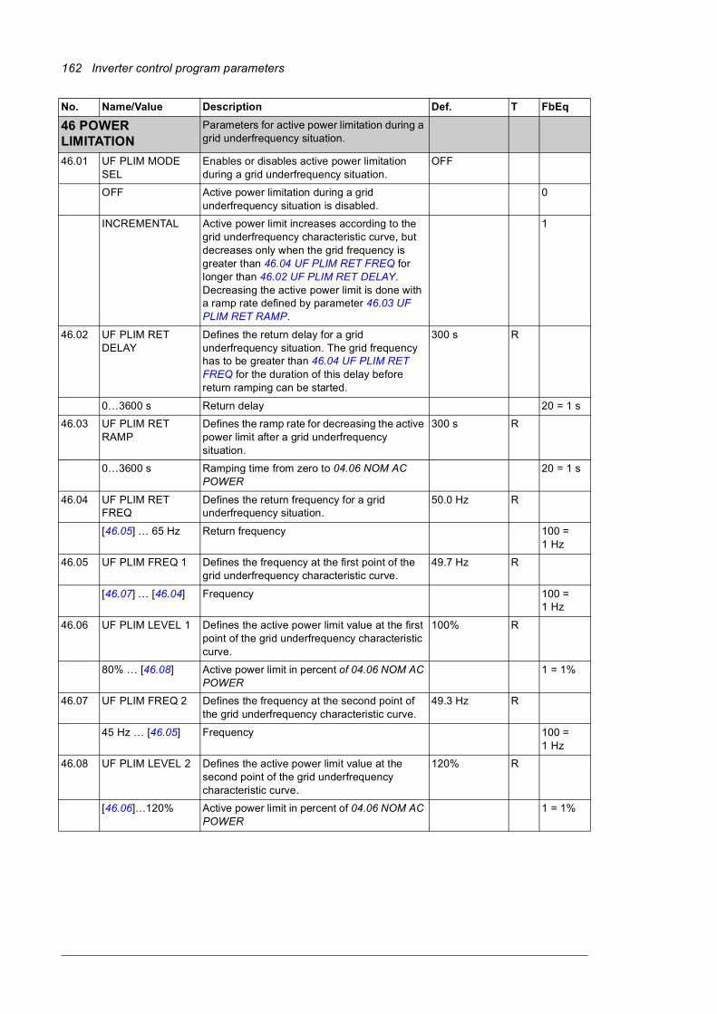
162 Inverter control program parameters
46 POWER LIMITATION
Parameters for active power limitation during a grid underfrequency situation.
46.01 UF PLIM MODE SEL
Enables or disables active power limitation during a grid underfrequency situation.
OFF
OFF Active power limitation during a grid underfrequency situation is disabled.
0
INCREMENTAL Active power limit increases according to the grid underfrequency characteristic curve, but decreases only when the grid frequency is greater than 46.04 UF PLIM RET FREQ for longer than 46.02 UF PLIM RET DELAY. Decreasing the active power limit is done with a ramp rate defined by parameter 46.03 UF PLIM RET RAMP.
1
46.02 UF PLIM RET DELAY
Defines the return delay for a grid underfrequency situation. The grid frequency has to be greater than 46.04 UF PLIM RET FREQ for the duration of this delay before return ramping can be started.
300 s R
0…3600 s Return delay 20 = 1 s
46.03 UF PLIM RET RAMP
Defines the ramp rate for decreasing the active power limit after a grid underfrequency situation.
300 s R
0…3600 s Ramping time from zero to 04.06 NOM AC POWER
20 = 1 s
46.04 UF PLIM RET FREQ
Defines the return frequency for a grid underfrequency situation.
50.0 Hz R
[46.05] … 65 Hz Return frequency 100 = 1 Hz
46.05 UF PLIM FREQ 1 Defines the frequency at the first point of the grid underfrequency characteristic curve.
49.7 Hz R
[46.07] … [46.04] Frequency 100 = 1 Hz
46.06 UF PLIM LEVEL 1 Defines the active power limit value at the first point of the grid underfrequency characteristic curve.
100% R
80% … [46.08] Active power limit in percent of 04.06 NOM AC POWER
1 = 1%
46.07 UF PLIM FREQ 2 Defines the frequency at the second point of the grid underfrequency characteristic curve.
49.3 Hz R
45 Hz … [46.05] Frequency 100 = 1 Hz
46.08 UF PLIM LEVEL 2 Defines the active power limit value at the second point of the grid underfrequency characteristic curve.
120% R
[46.06]…120% Active power limit in percent of 04.06 NOM AC POWER
1 = 1%
No. Name/Value Description Def. T FbEq

Inverter control program parameters 163
51 MASTER ADAPTER
These parameters are visible, and need to be adjusted, only when a fieldbus adapter module (optional) is installed and activated by parameter 98.02 COMM. MODULE. For details on the parameters, refer to the manual of the fieldbus module and chapter Fieldbus control.
Note: Any changes in these parameters take effect only after the next power-up of the adapter module.
51.01 MODULE TYPE Module type and software version
51.02…
51.26
FIELDBUS PAR2…26
(According to module type)
51.27 FBA PAR REFRESH
Validates any changed adapter module configuration parameter settings. After refreshing, the value reverts automatically to DONE.
DONE Refreshing done.
REFRESH Refreshing.
51.28 FILE CPI FW REV Displays the required CPI firmware revision of the fieldbus adapter as defined in the configuration file stored in the control unit memory. The CPI firmware version of the fieldbus adapter (refer to par. 51.32) must contain the same or a later CPI version to be compatible.
The format is xyz, where x = major revision, y = minor revision, z = correction number.
51.29 FILE CONFIG ID Displays the fieldbus adapter module configuration file identification stored in the control unit memory. This information is control program dependent.
51.30 FILE CONFIG REV Displays the fieldbus adapter module configuration file revision stored in the control unit memory.
The format is xyz, where x = major revision, y = minor revision, z = correction number.
51.31 FBA STATUS Displays the status of the adapter module.
IDLE Adapter not configured.
EXEC. INIT Adapter initializing.
TIME OUT Time-out has occurred in the communication between the adapter and the control unit.
CONFIG ERROR Adapter configuration error. The major or minor revision code of the CPI program revision on the control unit is not the revision required by the module (see parameter 51.32), or configuration file upload has failed more than five times.
OFF-LINE Adapter is off-line.
ON-LINE Adapter is on-line.
RESET Adapter is performing a hardware reset.
No. Name/Value Description Def. T FbEq

164 Inverter control program parameters
51.32 FBA CPI FW REV Displays the CPI program revision of the module inserted in slot 1 of the control unit.
The format is xyz, where x = major revision, y = minor revision, z = correction number.
51.33 FBA APPL FW REV
Displays the program revision of the module inserted in slot 1 of the control unit.
The format is xyz, where x = major revision, y = minor revision, z = correction number.
53 USER PARAMETERS
Adaptive program settings.
53.01 NUMERIC 1 Defines a numeric parameter for adaptive programming
0 PB
-8388608…8388607
Numeric value
53.02 NUMERIC 2 Defines a numeric parameter for adaptive programming
0 PB
-8388608…8388607
Numeric value
… … …
53.10 NUMERIC 10 Defines a numeric parameter for adaptive programming
0 PB
-8388608…8388607
Numeric value
53.11 STRING 1 Defines an alarm or fault text indication for the EVENT block
C
0…9 characters ASCII string type
53.12 STRING 2 Defines an alarm or fault text indication for the EVENT block
C
0…9 characters ASCII string type
… … …
53.17 STRING 7 Defines an alarm or fault text indication for the EVENT block
C
0…9 characters ASCII string type
57 ADAPTIVE PROG2 Adaptive program task 2 settings:
• selections of the function blocks and their input connections
• diagnostics.
57.01 STATUS Shows the value of adaptive program task 2 status word.
0 I
0…15 The table below shows the alternative bit states and the corresponding values on the control panel display.
If all the bits are FALSE (ie, 0), the state is STOPPED.
57.02 FAULTED PAR Points out the faulted parameter in adaptive program task 2.
0 P
No. Name/Value Description Def. T FbEq
Bit Display Meaning0 1 Running1 2 Editing2 4 Checking3 8 Faulted

Inverter control program parameters 165
0…32768 Value
57.05 BLOCK1 Selects the function block type for block 1 in adaptive program task 2.
NO I
0…32768 Function block type
57.06 INPUT1 Selects the source for input 1 of block 1. 0 P
-255.255.31 …
+255.255.31 /
C. -32768 … C. 32768
Parameter pointer or a constant value:
• Parameter pointer: Inversion, group, index and bit fields. The bit number is effective only for blocks handling Boolean inputs.
• Constant value: Inversion and constant fields. Inversion field must have value C to enable the constant setting.
Example: The state of digital input DI2 is connected to input 1 as follows:
• Set the source selection parameter (57.06) to +01.15.01. (The adaptive program stores the state of digital input DI2 to bit 1 of actual signal 01.15.)
• If you need an inverted value, switch the sign of the pointer value (-01.15.01).
57.07 INPUT2 Selects the source for input 2 of block 1. 0 P
See parameter 57.06 INPUT1.
57.08 INPUT3 Selects the source for input 3 of block 1. 0 P
See parameter 57.06 INPUT1.
57.09 OUTPUT Stores and displays the output of block 1. 0 I
0…32768 No user-setting possible
57.10 BLOCK2 Selects the function block type for block 2 in adaptive program task 2.
NO I
0…32768 Function block type
57.11 INPUT1 Selects the source for input 1 of block 2. 0 P
See parameter 57.06 INPUT1.
57.12 INPUT2 Selects the source for input 2 of block 2. 0 P
See parameter 57.06 INPUT1.
57.13 INPUT Selects the source for input 3 of block 2. 0 P
See parameter 57.06 INPUT1.
57.14 OUTPUT Stores and displays the output of block 2. 0 I
0…32768 No user setting possible
57.15 BLOCK3 Selects the function block type for block 3 in adaptive program task 2.
NO I
0…32768 Function block type
… …
57.104 OUTPUT Stores and displays the output of block 20. 0 I
0…32768 No user setting possible
58 ADAPT PROG2 CNTRL
Adaptive program task 2 control. The update time of task 2 control is 500 ms.
See parameter group 57 ADAPTIVE PROG2.
58.01 ADAPT PROG CMD
Selects the operation mode for adaptive program task 2.
EDIT I
STOP Stopped. The program can be edited. 1
No. Name/Value Description Def. T FbEq

166 Inverter control program parameters
START Running. The program cannot be edited. 2
EDIT Stops to edit the mode. The program can be edited.
3
58.02 EDIT CMD Selects the command for the block placed in the location defined by parameter 58.03 EDIT BLOCK. The program must be in editing mode (see parameter 58.01 ADAPT PROG CMD).
NO I
NO Home value. The value automatically reverts to NO after an editing command is executed.
1
PUSH Shifts the block in the location defined by parameter 58.03 EDIT BLOCK and the subsequent blocks one location up. A new block can be placed in the emptied location.
2
DELETE Selects the block in the location defined by parameter 58.03 EDIT BLOCK and shifts the subsequent blocks one step down.
3
PROTECT Activation of the task protection: Read-protects the input connections of the blocks. Activate as follows:
• Ensure the task operation mode is set to START or STOP (parameter 58.01 ADAPT PROG CMD).
• Set the passcode by parameter 58.05 PASSCODE.
• Set parameter 58.02 to PROTECT.
When protection is activated:
• All parameters in group 57 ADAPTIVE PROG2 excluding the block output parameters are hidden (read-protected).
• It is not possible to switch the task operating mode (parameter 58.01 ADAPT PROG CMD) to the editing mode.
• Parameter 58.05 PASSCODE value is set to 0.
4
UNPROTECT Deactivation of the task protection: no read protection of the input connection of the blocks. Deactivate as follows:
• Ensure the adaptive task operation mode is set to START or STOP (parameter 58.01 ADAPT PROG CMD).
• Set the passcode by parameter 58.05 PASSCODE.
• Set parameter 58.02 to UNPROTECT.
5
58.03 EDIT BLOCK Defines the block location number for the command selected by parameter 58.02 EDIT CMD.
0 I
1…15 Block location number
58.04 TIMELEV_SEL Indicates the fixed execution cycle time of 100 ms for adaptive program task 2.
500ms I
58.05 PASSCODE Defines the passcode, which activates/deactivates the protection of the input connections of the blocks. See parameter 58.02 EDIT CMD.
0 I
No. Name/Value Description Def. T FbEq

Inverter control program parameters 167
0h…FFFFFFh Passcode. The setting restores to 0 after the protection is activated/deactivated.
Note: When you activate the protection, write down the passcode and store it for later use.
70 DDCS CONTROL Settings for the fibre optic channels CH0, CH1 and CH3
70.01 CH0 NODE ADDR Defines the node address for DDCS channel CH0. No two nodes online may have the same address.
1 R
1…254 Node address 1 = 1
70.02 CH0 LINK CONTROL
Defines the light intensity of the transmission LEDs. LEDs act as light sources for option fibres which are connected to DDCS channel CH0.
With the maximum length of optic fibre cable, use value 15.
10 R
1…15 Light intensity 1 = 1
70.03 CH0 BAUD RATE Selects the communication speed of DDCS channel CH0. If FCI (Fieldbus Communication Interface) and fieldbus communication modules are used, parameter has to be set to 4 Mbit/s. Otherwise, the external control system sets the communication speed automatically.
4 Mbit/s I
8 Mbit/s 8 Mbit/s (not in use) 0
4 Mbit/s 4 Mbit/s 1
2 Mbit/s 2 Mbit/s (not in use) 2
1 Mbit/s 1 Mbit/s 3
70.04 CH0 TIMEOUT Defines the time delay before channel CH0 or type Rxxx fieldbus adapter interface communication break alarm/fault (COMM MODULE) is activated. Time count starts when the link fails to update the communication message. The action taken by the inverter on a communication break is defined by parameter 70.05 CH0 COM LOSS CTRL.
When parameter is set to zero, time is not monitored and COMM MODULE (7510) fault not generated regardless of the value of parameter 70.05 CH0 COM LOSS CTRL.
2000 ms R
0…60000 ms Time 1 = 1 ms
70.05 CH0 COM LOSS CTRL
Selects how the inverter reacts when communication error on DDCS channel CH0 or on type Rxxx fieldbus adapter interface is detected. Time delay for the communication break alarm/fault activation is defined by parameter 70.04 CH0 TIMEOUT.
Note: This parameter is in use when parameter 98.01 COMMAND SEL is set to MCW and external serial communication is activated by parameter 98.02 COMM. MODULE.
FAULT I
NO FAULT Inverter unit generates warning COMM MODULE (7510).
1
No. Name/Value Description Def. T FbEq

168 Inverter control program parameters
FAULT Inverter unit trips on fault COMM MODULE (7510).
2
70.06 CH1 LINK CONTROL
Defines the light intensity of the transmission LEDs. LEDs act as light sources for option fibres which are connected to DDCS channel CH1.
With the maximum length of optic fibre cable, use value 15.
10 R
1…15 Light intensity 1 = 1
70.15 CH3 NODE ADDR Defines the node address for DDCS channel CH3. No two nodes online may have the same address. Typically the setting needs to be changed when the inverter unit is connected in a ring configuration with other units and a PC with a DriveWindow PC tool.
Note: The new node address becomes valid only after the next power-up of the control unit.
2 R
1…254 Node address 1 = 1
70.16 CH3 LINK CONTROL
Defines the light intensity of the transmission LEDs. LEDs act as light sources for option fibres which are connected to DDCS channel CH3.
With the maximum length of optic fibre cable, use value 15.
15 R
1…15 Light intensity 1 = 1
70.19 CH0 HW CONNECTION
Selects the topology of the DDCS channel CH0 link.
Note: This parameter is not in use in the DriveBus mode.
STAR B
RING Devices are connected in a ring. 0
STAR Devices are connected in a star. 1
70.20 CH3 HW CONNECTION
Selects the topology of the DDCS channel CH3 link.
RING B
RING Devices are connected in a ring. 0
STAR Devices are connected in a star. 1
71 DRIVEBUS COMM DDCS channel CH0 DriveBus settings
71.01 CH0 DRIVEBUS MODE
Selects the communication mode for the DDCS channel CH0. The new mode becomes valid only after the next power-up of the PVS800. Data is exchanged 4 times faster in the DriveBus mode than in the DDCS mode.
NO B
NO DDCS mode 0
YES DriveBus mode 1
90 D SET REC ADDR Addresses into which the received data sets are written. These parameters should not be changed.
90.01 D SET 10 VAL 1 Selects the address into which data word 1 of data set 10 is written. Update time is 2 ms.
701 I
0…20000 Parameter index
90.02 D SET 10 VAL 2 Selects the address into which data word 2 of data set 10 is written. Update time is 2 ms.
15133 I
0…20000 Parameter index
No. Name/Value Description Def. T FbEq

Inverter control program parameters 169
90.03 D SET 10 VAL 3 Selects the address into which data word 3 of data set 10 is written. Update time is 2 ms.
0 I
0…20000 Parameter index
90.04 D SET 12 VAL 1 Selects the address into which data word 1 of data set 12 is written. Update time is 4 ms.
15110 I
0…20000 Parameter index
90.05 D SET 12 VAL 2 Selects the address into which data word 2 of data set 12 is written. Update time is 4 ms.
2402 I
0…20000 Parameter index
90.06 D SET 12 VAL 3 Selects the address into which data word 3 of data set 12 is written. Update time is 4 ms.
2403 I
0…20000 Parameter index
90.07 D SET 14 VAL 1 Selects the address into which data word 1 of data set 14 is written. Update time is 100 ms.
0 I
0…30000 Parameter index
90.08 D SET 14 VAL 2 Selects the address into which data word 2 of data set 14 is written. Update time is 100 ms.
3909 I
0…30000 Parameter index
90.09 D SET 14 VAL 3 Selects the address into which data word 3 of data set 14 is written. Update time is 100 ms.
15131 I
0…30000 Parameter index
90.10 D SET 16 VAL 1 Selects the address into which data word 1 of data set 16 is written. Update time is 100 ms.
0 I
0…30000 Parameter index
90.11 D SET 16 VAL 2 Selects the address into which data word 2 of data set 16 is written. Update time is 100 ms.
0 I
0…30000 Parameter index
90.12 D SET 16 VAL 3 Selects the address into which data word 3 of data set 16 is written. Update time is 100 ms.
0 I
0…30000 Parameter index
90.13 D SET 18 VAL 1 Selects the address into which data word 1 of data set 18 is written. Update time is 500 ms.
0 I
0…30000 Parameter index
90.14 D SET 18 VAL 2 Selects the address into which data word 2 of data set 18 is written. Update time is 500 ms.
0 I
0…30000 Parameter index
90.15 D SET 18 VAL 3 Selects the address into which data word 3 of data set 18 is written. Update time is 500 ms.
0 I
0…30000 Parameter index
90.16 D SET 20 VAL 1 Selects the address into which data word 1 of data set 20 is written. Update time is 500 ms.
0 I
0…30000 Parameter index
90.17 D SET 20 VAL 2 Selects the address into which data word 2 of data set 20 is
written. Update time is 500 ms.
0 I
0…30000 Parameter index
90.18 D SET 20 VAL 3 Selects the address into which data word 3 of data set 20 is written. Update time is 500 ms.
0 I
0…30000 Parameter index
No. Name/Value Description Def. T FbEq

170 Inverter control program parameters
91 D SET REC ADDR See 90 D SET REC ADDR.
91.01 D SET 22 VAL 1 Selects the address into which data word 1 of data set 22 is written. Update time is 500 ms.
0 I
0…30000 Parameter index
… … … … …
91.06 D SET 24 VAL 3 Selects the address into which data word 3 of data set 24 is written. Update time is 500 ms.
0 I
0…30000 Parameter index
92 D SET TR ADDR Datasets which the inverter units sends to the master station. These parameters should not be changed.
92.01 D SET 11 VAL 1 Selects the address from which data word 1 of data set 11 is read. Update time is 2 ms.
801 I
0…20000 Parameter index
92.02 D SET 11 VAL 2 Selects the address from which data word 2 of data set 11 is read. Update time is 2 ms.
15205 I
0…20000 Parameter index
92.03 D SET 11 VAL 3 Selects the address from which data word 3 of data set 11 is read. Update time is 2 ms.
15204 I
0…20000 Parameter index
92.04 D SET 13 VAL 1 Selects the address from which data word 1 of data set 13 is read. Update time is 4 ms.
15109 I
0…20000 Parameter index
92.05 D SET 13 VAL 2 Selects the address from which data word 2 of data set 13 is read. Update time is 4 ms.
218 I
0…20000 Parameter index
92.06 D SET 13 VAL 3 Selects the address from which data word 3 of data set 13 is read. Update time is 4 ms.
201 I
0…20000 Parameter index
92.07 D SET 15 VAL 1 Selects the address from which data word 1 of data set 15 is read. Update time is 100 ms.
930 I
0…30000 Parameter index
92.08 D SET 15 VAL 2 Selects the address from which data word 2 of data set 15 is read. Update time is 100 ms.
130 I
0…30000 Parameter index
92.09 D SET 15 VAL 3 Selects the address from which data word 3 of data set 15 is read. Update time is 100 ms.
112 I
0…30000 Parameter index
92.10 D SET 17 VAL 1 Selects the address from which data word 1 of data set 17 is read. Update time is 100 ms.
911 I
0…30000 Parameter index
92.11 D SET 17 VAL 2 Selects the address from which data word 2 of data set 17 is read. Update time is 100 ms.
912 I
0…30000 Parameter index
92.12 D SET 17 VAL 3 Selects the address from which data word 3 of data set 17 is read. Update time is 100 ms.
117 I
0…30000 Parameter index
92.13 D SET 19 VAL 1 Selects the address from which data word 1 of data set 19 is read. Update time is 500 ms.
806 I
0…30000 Parameter index
No. Name/Value Description Def. T FbEq

Inverter control program parameters 171
92.14 D SET 19 VAL 2 Selects the address from which data word 2 of data set 19 is read. Update time is 500 ms.
109 I
0…30000 Parameter index
92.15 D SET 19 VAL 3 Selects the address from which data word 3 of data set 19 is read. Update time is 500 ms.
113 I
0…30000 Parameter index
92.16 D SET 21 VAL 1 Selects the address from which data word 1 of data set 21 is read. Update time is 500 ms.
15201 I
0…30000 Parameter index
92.17 D SET 21 VAL 2 Selects the address from which data word 2 of data set 21 is read. Update time is 500 ms.
15202 I
0…30000 Parameter index
92.18 D SET 21 VAL 3 Selects the address from which data word 3 of data set 21 is read. Update time is 500 ms.
15203 I
0…30000 Parameter index
93 D SET TR ADDR Datasets which the inverter units sends to the master station. Datasets 25 and 35 can be freely used to transmit arbitrary parameter values from the Inverter control program to the Master control program.
93.01 D SET 23 VAL 1 Selects the address from which data word 1 of data set 23 is read. Update time is 500 ms.
910 I
0…30000 Parameter index
93.02 D SET 23 VAL 2 Selects the address from which data word 2 of data set 23 is read. Update time is 500 ms.
406 I
0…30000 Parameter index
93.03 D SET 23 VAL 3 Selects the address from which data word 3 of data set 23 is read. Update time is 500 ms.
15119 I
0…30000 Parameter index
93.04 D SET 25 VAL 1 Selects the address from which data word 1 of data set 25 is read. Update time is 500 ms.
0 I
0…30000 Parameter index
93.05 D SET 25 VAL 2 Selects the address from which data word 2 of data set 25 is read. Update time is 500 ms.
0 I
0…30000 Parameter index
93.06 D SET 25 VAL 3 Selects the address from which data word 3 of data set 25 is read. Update time is 500 ms.
0 I
0…30000 Parameter index
93.07 D SET 27 VAL 1 Selects the address from which data word 1 of data set 27 is read. Update time is 500 ms.
214 I
93.08 D SET 27 VAL 2 Selects the address from which data word 2 of data set 27 is read. Update time is 500 ms.
215 I
93.09 D SET 27 VAL 3 Selects the address from which data word 3 of data set 27 is read. Update time is 500 ms.
216 I
93.10 D SET 29 VAL 1 Selects the address from which data word 1 of data set 29 is read. Update time is 500 ms.
127 I
93.11 D SET 29 VAL 2 Selects the address from which data word 2 of data set 29 is read. Update time is 500 ms.
803 I
93.12 D SET 29 VAL 3 Selects the address from which data word 3 of data set 29 is read. Update time is 500 ms.
111 I
No. Name/Value Description Def. T FbEq

172 Inverter control program parameters
93.13 D SET 31 VAL 1 Selects the address from which data word 1 of data set 31 is read. Update time is 500 ms.
202 I
93.14 D SET 31 VAL 2 Selects the address from which data word 2 of data set 31 is read. Update time is 500 ms.
203 I
93.15 D SET 31 VAL 3 Selects the address from which data word 3 of data set 31 is read. Update time is 500 ms.
129 I
93.16 D SET 35 VAL 1 Selects the address from which data word 1 of data set 33 is read. Update time is 500 ms.
13501 I
93.17 D SET 35 VAL 2 Selects the address from which data word 2 of data set 33 is read. Update time is 500 ms.
0 I
93.18 D SET 35 VAL 3 Selects the address from which data word 3 of data set 33 is read. Update time is 500 ms.
0 I
98 OPTION MODULES
Activation of external serial communication. See chapter Fieldbus control.
98.01 COMMAND SEL Selects the control command interface(s). See parameter 98.02 COMM. MODULE.
MCW B
MCW Via a serial link and through digital input terminals
0
I/O Through digital input terminals 1
98.02 COMM. MODULE Activates the external serial communication and selects the interface. This parameter should not be changed.
PVA I
NO Reserved 1
FIELDBUS Reserved 2
ADVANT/N-FB Reserved 3
STD MODBUS Reserved 4
PVA Inverter unit is controlled by the master control unit.
5
98.09 DI/O EXT MODULE 1
Activates the communication to optional digital I/O extension module 1 and defines the type and connection interface of the module. See signal 08.05 DI STATUS WORD.
Note: With PVS800, an RDIO module is installed as standard into slot 1. The usage of the module is described in the hardware manual.
Faster DC input signal detection can be achieved by disabling the hardware filter of the digital input with the configuration DIP switch on the circuit board of the module.
Note: Always enable the hardware filtering with an AC input signal.
For more information, see RDIO-01 Digital I/O Extension User's Manual [3AFE64485733 (English)].
RDIO-SLOT2 I
NOT IN USE Inactive 2
No. Name/Value Description Def. T FbEq
ON
1 2 3 4
EnabledDisabled
DI1DI2DI3
Hardware filtering
DIP switch S2 (RDIO)

Inverter control program parameters 173
RDIO-SLOT1 Communication active. Module type: RDIO. Connection interface: Inverter control unit slot 1.
3
RDIO-SLOT2 Communication active. Module type: RDIO. Connection interface: Inverter control unit slot 2.
4
RDIO-DDCS Communication active. Module type: RDIO. Connection interface: Optional I/O module adapter (AIMA) that communicates with the inverter control unit through fiber optic link CH1.
Note: Module node number must be set to 2 with switch S1.
5
98.10 DI/O EXT MODULE 2
Activates the communication to optional digital I/O extension module 2 and defines the type and connection interface of the module. See signals 08.05 DI STATUS WORD.
Note: With 500kW PVS800 units, an RDIO module is installed as standard into slot 2. The usage of the module is described in the hardware manual.
Faster DC input signal detection can be achieved by disabling the hardware filter of the digital input with the configuration DIP switch on the circuit board of the module.
Note: Always enable the hardware filtering with an AC input signal.
The default value is 2 (NOT IN USE) with 100 and 250 kW inverters, 3 (RDIO-SLOT1) with 500 kW inverters.
For more information, see RDIO-01 Digital I/O Extension User's Manual [3AFE64485733 (English)].
NOT IN USE I
NOT IN USE Inactive 2
RDIO-SLOT1 Communication active. Module type: RDIO. Connection interface: Inverter control unit slot 1.
3
RDIO-SLOT2 Communication active. Module type: RDIO. Connection interface: Inverter control unit slot 2.
4
RDIO-DDCS Communication active. Module type: RDIO. Connection interface: Optional I/O module adapter (AIMA) that communicates with the inverter control unit through fiber optic link CH1.
Note: Module node number must be set to 3 with switch S1.
5
No. Name/Value Description Def. T FbEq
Switch S1
AB
C D E F 01
2
345678
9
ON
1 2 3 4
EnabledDisabled
DI1DI2DI3
Hardware filtering
DIP switch S2 (RDIO)
Switch S1
AB
C D E F 01
2
345678
9

174 Inverter control program parameters
98.11 AI/O EXT MODULE 1
Activates the communication to the optional analog I/O extension module 1.
NOT IN USE I
NOT IN USE Inactive. 2
RAIO-SLOT1 Communication active. Module type: RAIO. 3
RAIO-SLOT2 Communication active. Module type: RAIO. 4
RAIO-DDCS Communication active. Module type: RAIO. Connection interface: Optional I/O module adapter (AIMA) that communicates with the inverter control unit through fiber optic link CH1.
Note: Module node number must be set to 5 with switch S1.
5
98.15 AI/O EXT MODULE 2
Activates the communication to the optional analog I/O extension module 2.
NOT IN USE I
NOT IN USE Inactive 2
RAIO-SLOT1 Communication active. Module type: RAIO. 3
RAIO-SLOT2 Communication active. Module type: RAIO. 4
RAIO-DDCS Communication active. Module type: RAIO. Connection interface: Optional I/O module adapter (AIMA) that communicates with the inverter control unit through fiber optic link CH1.
Note: Module node number must be set to 6 with switch S1.
5
99 START-UP DATA Language, identification run selection etc.
99.01 LANGUAGE Selects the display language. ENGLISH I
ENGLISH English 0
DEUTSCH German 2
99.02 DEVICE NAME Defines the name for the inverter unit. The name is visible on the control panel display in the Control Unit Selection mode or on the DriveWindow main menu.
Note: The name can be typed only by using a PC tool.
C
Name
99.06 FAST SYNC Activates the fast synchronization of the inverter unit at start.
YES B
NO Inactive: synchronisation with phase order check
0
YES Active: synchronisation without phase order check
1
99.07 LINE SIDE ID RUN Enables/disables manual grid identification. See section Grid identification on page 35.
YES B
NO Disabled 0
YES Enabled. The identification starts when the inverter unit receives a start command. (Identification takes about 4 seconds. It is not allowed to load the inverter unit during the identification.)
1
No. Name/Value Description Def. T FbEq
Switch S1
AB
C D E F 01
2
345678
9
Switch S1
AB
C D E F 01
2
345678
9

Inverter control program parameters 175
99.08 AUTO LINE ID RUN
Enables/disables automatic grid identification. See section Grid identification on page 35.
Note: Automatic identification can be disabled after a successful ID run unless the phase order has changed afterwards.
YES B
NO Disabled 0
YES Enabled. The identification is requested automatically after control unit power-up. The identification starts automatically when the inverter receives the start command. The parameter actually forces parameter 99.07 LINE SIDE ID RUN to YES. Identification takes about 4 seconds. It is not allowed to load the inverter during the identification procedure.
1
99.09 APPLIC RESTORE Restores the original parameter settings. NO B
NO No 0
YES Yes 1
99.10 SUPPLY ID NUMBER
This parameter can be used by an external control system to check the right connections of the optical cables to the inverter unit. This parameter requires support from the external control system to verify the correct connection.
0 I
0…32767
No. Name/Value Description Def. T FbEq

176 Inverter control program parameters

Fault tracing 177
7
Fault tracing
What this chapter containsThis chapter lists all alarm and fault messages including the possible causes and corrective actions.
Safety
WARNING! Only qualified electricians are allowed to service the PVS800. Read the safety instructions in the appropriate hardware manual before working on the PVS800.
Alarm and fault indicationsAn alarm or a fault message indicates abnormal PVS800 status. Most alarm and fault causes can be identified and corrected using this information. If not, an ABB representative should be contacted.
The four digit code number in brackets after the message is for fieldbus communication. See chapter Fieldbus control.
How to resetThe PVS800 (master and inverter control units) can be reset either from DriveWindow, by pressing the keypad RESET key, by fieldbus, or switching the power off for a while. When the fault is removed, the inverter can be restarted.

178 Fault tracing
Fault historyWhen a fault is detected, it is stored in the fault history. The latest faults and alarms are stored together with the time stamp at which the event was detected.
The fault logger collects 64 of the latest faults. When the control unit power is switched off, 16 of the latest faults are stored.
The Fault History can be viewed using DriveWindow or by pressing the control panel
double arrow keys ( or ) in the Actual Signal Display mode. The fault history can
then be scrolled with arrow keys ( and ). To exit the fault history press an arrow key
( or ). The fault history can be cleared by pressing the RESET key.

Fault tracing 179
Alarm and fault messages generated by the master control programThe parameter numbers and names in the table refer to the master control program unless otherwise indicated.
Note: When viewing the fault history of the master control program, fault and alarm messages originating in the inverter control program are preceded by a “>” sign.
Message
Ala
rm
Fa
ult Cause What to do
>ANTI-ISLAND (819F)
09.14 PVA FAULT WORD bit 12
Island operation is detected in the grid.
Check the grid condition.
Check group 45 ANTI-ISLANDING.
ALM (xx)
08.01 MAIN STATUS WORD bit 7
Internal alarm. Write down the code in brackets. Contact an ABB service representative.
ANALOG IO (5441)
09.10 IO FAULT WORD bit 13
Analog input error detected on the control unit.
Replace the control unit.
APPLIC 1 FLT (FFD6)
09.15 PVA ALARM WORD bit 13
Adaptive program task alarm Download adaptive program 1 using DriveAP 2.x or set block parameters by control panel or DriveWindow
APPLIC 2 FLT (FFD7)
09.15 PVA ALARM WORD bit 14
Adaptive program task alarm Download adaptive program 2 using DriveAP 2.x or set block parameters by control panel or DriveWindow
APP OVERLOAD (FFD9)
09.15 PVA ALARM WORD bit 12
Application software overload. There is not enough processor capacity to execute blocks.
Reduce application software load, for example,
• move some blocks to slower time level
• disable point to point communication
• disable some extension modules.
AUTORESET A (6081)
09.15 PVA ALARM WORD bit 3
A sequence of automatic fault resets is in progress.
See parameter 30.05 NUMBER OF TRIALS (page 78).
Check the fault log.
AUTORESET F (6080)
09.14 PVA FAULT WORD bit 8
The end of a sequence of automatic fault resets is reached.
See parameter 30.05 NUMBER OF TRIALS (page 78).
Check the fault log.
>BACKPOW LEV (818E)
09.14 PVA FAULT WORD bit 7
See REVERSE POW (8187) (page 193)
BACKUP ERROR (FFA2) Failure in restoring PC-stored backup of parameters.
Retry.
Check connections.
Check that the parameters are compatible with the control program.
BACKUP USED (FFA3) PC-stored backup of parameters is downloaded into the control unit.
Wait until download is completed.
>CHARGING F (3284)
09.11 SUPPLY FAULT WORD bit 0
See CHARGING FLT (3230) (page 187)

180 Fault tracing
CH2 COM LOSS (7520)
09.14 PVA FAULT WORD bit 1
Communication error in CH2 between master and inverter control units.
Check that CH0 address in the inverter control program is correct.
Check fibre optic cables between master and inverter control units.
Check that the inverter control unit is powered.
Replace fibre optic cables.
COMM MODULE (7510)
09.14 PVA FAULT WORD bit 0
Programmable fault: Parameter 70.05
Cyclical communication between the master control unit and an external control unit (for example, a PLC) is lost.
External communication was activated with parameter
Check fieldbus communication status. See chapter Fieldbus control, or appropriate fieldbus adapter manual.
Check group 51 MASTER ADAPTER (fieldbus adapter) parameter settings.
Check that the bus master is communicating and correctly configured.
Check cable connections and groundings.
>COMM MODULE (7581)
09.11 SUPPLY FAULT WORD bit 10
See COMM MODULE (7510) (page 187)
>COMM MODULE (758A)
CTRL B TEMP (4110) Control unit temperature exceeds 88 °C.
Check air flow and fan operation.
>DC BRK LEV (818C)
09.14 PVA FAULT WORD bit 5
See DC SWITCH LEV (818C) (page 188)
>DC BRK POS (818D)
09.14 PVA FAULT WORD bit 6
See DC SWITCH POS (818D) (page 188)
>DC BRK TRP (8188)
09.14 PVA FAULT WORD bit 3
See DC SWITCH TRP (8188) (page 188)
DC INPUT DEV (2185)
09.15 PVA ALARM WORD bit 4
Programmable fault: Parameter 26.06
A current deviation occurred in one or more of the DC inputs.
Identify the deviating DC inputs in parameter 26.04 DC INPUT STATUS. Then, check the wiring of the deviating DC inputs.
DC OVERVOLT (32AF)
09.11 SUPPLY FAULT WORD bit 15
DC overvoltage measured by the inverter module. Limit is 1000 V.
Check the level of the DC voltage.
>DC UNDERVLT (3282)
09.11 SUPPLY FAULT WORD bit 14
See DC UNDERVOLT (3220) (page 188).
DIGITAL IO (5442)
09.10 IO FAULT WORD bit 5
Digital I/O fault in the control unit. Replace the control unit.
>EARTH FAULT (2383)
09.11 SUPPLY FAULT WORD bit 12
See EARTH FAULT (2387) (page 189), CUR UNBAL (2330) (page 187), CUR UNBAL 1 (23E0) (page 187), CUR UNBAL 2 (23E1) (page 187) or CUR UNBAL 3 (23E2) (page 187).
EM STOP (F081)
Programmable fault: Parameter 30.10
Emergency stop circuit is open. Check the emergency stop circuit.
Check the connection to digital input 6 (DI6).
EM STOP (F083)
09.14 PVA FAULT WORD bit 13
Programmable fault: Parameter 30.10
Message
Ala
rm
Fa
ult Cause What to do

Fault tracing 181
EXT AIO (7081)
09.10 IO FAULT WORD bit 14
Analog I/O error on RAIO I/O Extension module.
Check cabinet temperature.
If RAIO is installed on the AIMA board, check the optical wires between the control unit and AIMA.
Check the rotary address switch of the RAIO.
If alarm persists, replace the RAIO module.
EXT DIO (7082)
09.10 IO FAULT WORD bit 6
Digital input error on RDIO I/O Extension module.
Check cabinet temperature.
Replace RDIO module if alarm persists.
>EXT DI1 (1082)
09.11 SUPPLY FAULT WORD bit 5
See DI1 (9088) (page 188).
>EXT DI1 ALM (1089) See DI1 (9081) (page 188).
>EXT DI4 (1080)
09.11 SUPPLY FAULT WORD bit 4
See EXT EVENT DI4 (9084) (page 189).
>EXT DI4 ALM (108A) See EXT EVNT DI4 (908B) (page 189).
>EXT DI5 (1081)
09.11 SUPPLY FAULT WORD bit 2
See EXT EVENT DI5 (9085) (page 189).
>EXT DI5 ALM (108B) See EXT EVNT DI5 (908C) (page 190).
>EXT DI7 (FF96)
09.11 SUPPLY FAULT WORD bit 11
See EXT EVENT DI7 (9087) (page 189).
>EXT DI7 ALM (108C) See EXT EVNT DI7 (908E) (page 190).
EXT EVNT DI3 (9083)
09.15 PVA ALARM WORD bit 7
State of digital input DI3 changed to 0.
By default, this message indicates the triggering of hardware overvoltage protection.
Check state of digital input DI3.
Check setting of parameter 30.01 DI3 EXT EVENT.
Check and replace overvoltage protection devices.
EXT EVNT DI3 (9083)
09.14 PVA FAULT WORD bit 9
EXT EVNT DI4 (9084)
09.15 PVA ALARM WORD bit 8
State of digital input DI4 changed to 0.
By default, this message indicates the blown-out DC fuse (if option +G420 is installed).
Check state of digital input DI4.
Check setting of parameter 30.02 DI4 EXT EVENT.EXT EVNT DI4 (9084)
09.14 PVA FAULT WORD bit 10
EXT EVNT DI5 (9085)
09.15 PVA ALARM WORD bit 9
State of digital input DI5 changed to 0.
By default, this digital input is not used.
Check state of digital input DI5.
Check setting of parameter 30.03 DI5 EXT EVENT.EXT EVNT DI5 (9085)
09.14 PVA FAULT WORD bit 11
FACTORY FILE (FFA7) Factory macro parameter error. Replace RMIO board or RDCU control unit.
FLT (xx)
08.01 MAIN STATUS WORD bit 3
Internal fault. Write down the fault code in brackets. Contact ABB service.
GND CLOSE ER (8196) Grounding disconnector was not properly closed. This may be caused by:
• Wrong DC to the ground voltage status
• Too high continuous leakage current
Check that the selected grounding resistance is suitable with the solar modules in use.
Message
Ala
rm
Fa
ult Cause What to do
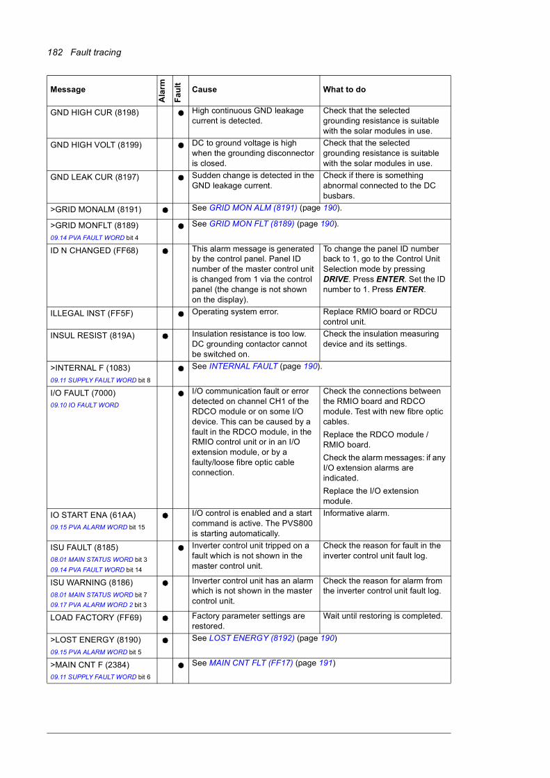
182 Fault tracing
GND HIGH CUR (8198) High continuous GND leakage current is detected.
Check that the selected grounding resistance is suitable with the solar modules in use.
GND HIGH VOLT (8199) DC to ground voltage is high when the grounding disconnector is closed.
Check that the selected grounding resistance is suitable with the solar modules in use.
GND LEAK CUR (8197) Sudden change is detected in the GND leakage current.
Check if there is something abnormal connected to the DC busbars.
>GRID MONALM (8191) See GRID MON ALM (8191) (page 190).
>GRID MONFLT (8189)
09.14 PVA FAULT WORD bit 4
See GRID MON FLT (8189) (page 190).
ID N CHANGED (FF68) This alarm message is generated by the control panel. Panel ID number of the master control unit is changed from 1 via the control panel (the change is not shown on the display).
To change the panel ID number back to 1, go to the Control Unit Selection mode by pressing DRIVE. Press ENTER. Set the ID number to 1. Press ENTER.
ILLEGAL INST (FF5F) Operating system error. Replace RMIO board or RDCU control unit.
INSUL RESIST (819A) Insulation resistance is too low. DC grounding contactor cannot be switched on.
Check the insulation measuring device and its settings.
>INTERNAL F (1083)
09.11 SUPPLY FAULT WORD bit 8
See INTERNAL FAULT (page 190).
I/O FAULT (7000)
09.10 IO FAULT WORD
I/O communication fault or error detected on channel CH1 of the RDCO module or on some I/O device. This can be caused by a fault in the RDCO module, in the RMIO control unit or in an I/O extension module, or by a faulty/loose fibre optic cable connection.
Check the connections between the RMIO board and RDCO module. Test with new fibre optic cables.
Replace the RDCO module / RMIO board.
Check the alarm messages: if any I/O extension alarms are indicated.
Replace the I/O extension module.
IO START ENA (61AA)
09.15 PVA ALARM WORD bit 15
I/O control is enabled and a start command is active. The PVS800 is starting automatically.
Informative alarm.
ISU FAULT (8185)
08.01 MAIN STATUS WORD bit 3
09.14 PVA FAULT WORD bit 14
Inverter control unit tripped on a fault which is not shown in the master control unit.
Check the reason for fault in the inverter control unit fault log.
ISU WARNING (8186)
08.01 MAIN STATUS WORD bit 7
09.17 PVA ALARM WORD 2 bit 3
Inverter control unit has an alarm which is not shown in the master control unit.
Check the reason for alarm from the inverter control unit fault log.
LOAD FACTORY (FF69) Factory parameter settings are restored.
Wait until restoring is completed.
>LOST ENERGY (8190)
09.15 PVA ALARM WORD bit 5
See LOST ENERGY (8192) (page 190)
>MAIN CNT F (2384)
09.11 SUPPLY FAULT WORD bit 6
See MAIN CNT FLT (FF17) (page 191)
Message
Ala
rm
Fa
ult Cause What to do

Fault tracing 183
>MPPT MAX REF (32AE)
09.17 PVA ALARM WORD 2 bit 1
DC voltage reference is at the MPPT high limit. This may be caused by incorrect sizing of the solar array or by power limitation.
Check the external DC voltage reference in parameter 32.01 EXT MPPT DC REF.
Check the sizing of the solar array.
Check the power limitation in parameter 31.16 POWER LIMITING.
>MPPT MIN REF (32AD)
09.17 PVA ALARM WORD 2 bit 0
DC voltage reference is at the MPPT low limit.
Check the external DC voltage reference in parameter 23.01 EXT MPPT DC REF.
>NET LOST (32A6) See NET LOST (32A3) (page 191)
>NET VOLT (3285)
09.11 SUPPLY FAULT WORD bit 9
See NET VOLT FLT (3100)/(32A2) (page 191)
NO COMMUNICATION This alarm message is generated by the CDP312R control panel.
Detected problem in cable or hardware malfunction on the CDP312R control panel link.
If (×) = 4, control panel type is not compatible with the master control program version.
Check the CDP312R control panel link connections.
Press RESET key. Reset may take up to half a minute. Please wait.
Check control panel type and version of the master control program (see parameter group 04 INFORMATION). The panel type is printed on the panel housing.
>OVERCURR (2380)
09.11 SUPPLY FAULT WORD bit 1
See OVERCURRENT (2310) (page 191)
PANEL LOST (5300)
09.12 SUPPLY ALARM WORD bit 1
Local control device (CDP312R control panel or DriveWindow PC tool) selected as active control location has stopped communicating.
Note: PVS800 shifts to remote control mode automatically.
Check the CDP312R control panel and PC connections.
Check the CDP312R control panel connector. See the hardware manual.
Replace control panel.
>PANEL LOST (5382) See PANEL LOST (5300) (page 192)
PARAM CRC (6320) CRC (Cyclic Redundancy Check) error.
Switch control unit power off and on again.
Reload firmware onto control unit.
Replace control unit.
>PLIM EXT TMP (44AB) Active power is limited due to high ambient temperature.
Check the cooling of the inverter.
POWFAIL FILE (FFA0) Error in restoring powerfail.ddf file If the alarm persists, replace RMIO board or RDCU control unit.
PVA RUN ENA (FF54)
09.15 PVA ALARM WORD bit 2
A start command was given while stand by was forced with parameter 31.01 ENABLE MPPT or while bit 3 in parameter 08.05 PVA STATUS WORD is 0.
Check the setting of parameter 31.01 ENABLE MPPT.
>PVS&PANEL DC (32A9)
09.15 PVA ALARM WORD bit 1
See PVS&PANEL DC (32A8) (page 192)
>PVS800 TEMP (4291)
09.11 SUPPLY FAULT WORD bit 3
See PVS800 TEMP (4294) (page 193)
>PVS800 TEMP (4292)
Message
Ala
rm
Fa
ult Cause What to do

184 Fault tracing
>QLIM PVS TMP (818F) Reactive power is limited due to high inverter temperature.
Check the cooling of the inverter.
Check air flow and fan operation.
Check heatsink fins for dust pick-up.
Check line current against inverter nominal current.
>QLIM EXT TMP (44AC) Reactive power is limited due to high ambient temperature.
Check the cooling of the inverter.
>RECHARGE ALM (32AA) See RECHARGE ALM (3250) (page 193)
>REVERSE POW (8187)
09.14 PVA FAULT WORD bit 2
See REVERSE POW (8187) (page 193)
RMBA LOST (61A9)
09.15 PVA ALARM WORD bit 11
String monitoring is activated but no RMBA module is installed to RDCU slot 2.
Install and activate RMBA.
>RUN DISABLE (8194) Hardware run enable signal is missing from the inverter control unit DI2.
Cut-in conditions are not fulfilled.
Check emergency stop circuit.
Check the cut-in settings with parameters 44.18…44.23.
Check that the hand-operated DC switch Q2 is switched on.
Check actual values of voltage and frequency with parameters 01.11 MAINS VOLTAGE and 02.18 GRID FREQUENCY.
>SHORT CIRC (2381)
09.11 SUPPLY FAULT WORD bit 7
See SHORT CIRC (2340) (page 194)
SBOX 1 LINK (6195)SBOX 2 LINK (6196)SBOX 3 LINK (6197)…
SBOX 20 LINK (61A8)
Communication with string box channel x (1…20) lost.
Check the wiring of the affected channel.
Check also the line termination and node addresses.
>SYNCHRO FLT (8180)
09.11 SUPPLY FAULT WORD bit 13
See SYNCHRO FLT (8180) (page 194)
SYSTEM START (1087) Control program is started (control unit is powered).
If this message appears during normal operation, check the 24 V supply to the control unit. Check the wiring for breakages and short circuits.
UDC HIGH LIM (32A7)
09.15 PVA ALARM WORD bit 6
Measured DC voltage exceeds high limit.
See DC overvoltage monitoring (page 35).
Message
Ala
rm
Fa
ult Cause What to do
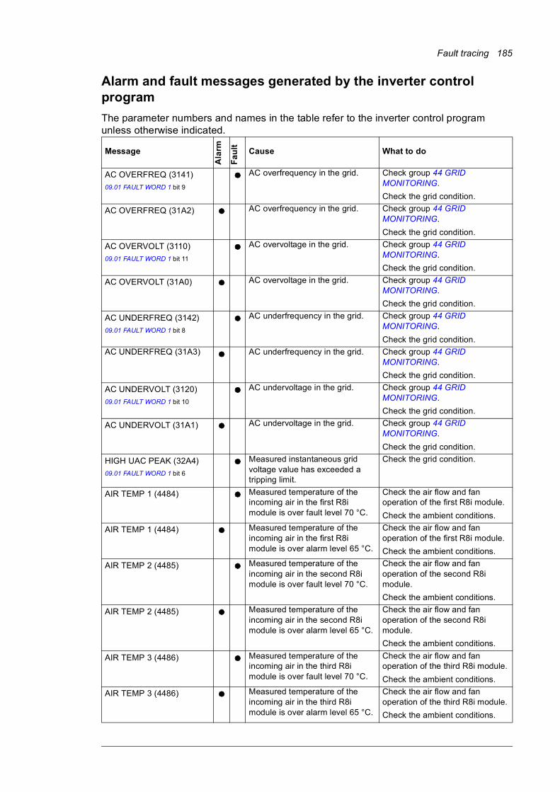
Fault tracing 185
Alarm and fault messages generated by the inverter control program
The parameter numbers and names in the table refer to the inverter control program unless otherwise indicated.
Message
Ala
rm
Fa
ult Cause What to do
AC OVERFREQ (3141)
09.01 FAULT WORD 1 bit 9
AC overfrequency in the grid. Check group 44 GRID MONITORING.
Check the grid condition.
AC OVERFREQ (31A2) AC overfrequency in the grid. Check group 44 GRID MONITORING.
Check the grid condition.
AC OVERVOLT (3110)
09.01 FAULT WORD 1 bit 11
AC overvoltage in the grid. Check group 44 GRID MONITORING.
Check the grid condition.
AC OVERVOLT (31A0) AC overvoltage in the grid. Check group 44 GRID MONITORING.
Check the grid condition.
AC UNDERFREQ (3142)
09.01 FAULT WORD 1 bit 8
AC underfrequency in the grid. Check group 44 GRID MONITORING.
Check the grid condition.
AC UNDERFREQ (31A3) AC underfrequency in the grid. Check group 44 GRID MONITORING.
Check the grid condition.
AC UNDERVOLT (3120)
09.01 FAULT WORD 1 bit 10
AC undervoltage in the grid. Check group 44 GRID MONITORING.
Check the grid condition.
AC UNDERVOLT (31A1) AC undervoltage in the grid. Check group 44 GRID MONITORING.
Check the grid condition.
HIGH UAC PEAK (32A4)
09.01 FAULT WORD 1 bit 6
Measured instantaneous grid voltage value has exceeded a tripping limit.
Check the grid condition.
AIR TEMP 1 (4484) Measured temperature of the incoming air in the first R8i module is over fault level 70 °C.
Check the air flow and fan operation of the first R8i module.
Check the ambient conditions.
AIR TEMP 1 (4484) Measured temperature of the incoming air in the first R8i module is over alarm level 65 °C.
Check the air flow and fan operation of the first R8i module.
Check the ambient conditions.
AIR TEMP 2 (4485) Measured temperature of the incoming air in the second R8i module is over fault level 70 °C.
Check the air flow and fan operation of the second R8i module.
Check the ambient conditions.
AIR TEMP 2 (4485) Measured temperature of the incoming air in the second R8i module is over alarm level 65 °C.
Check the air flow and fan operation of the second R8i module.
Check the ambient conditions.
AIR TEMP 3 (4486) Measured temperature of the incoming air in the third R8i module is over fault level 70 °C.
Check the air flow and fan operation of the third R8i module.
Check the ambient conditions.
AIR TEMP 3 (4486) Measured temperature of the incoming air in the third R8i module is over alarm level 65 °C.
Check the air flow and fan operation of the third R8i module.
Check the ambient conditions.

186 Fault tracing
ALM (xx)
08.01 MAIN STATUS WORD bit 7
Inverter internal alarm Check the connections of the inverter unit.
Write down alarm code (in brackets). Contact an ABB service representative.
ANTI-ISLAND (81A0)
08.06 MPPT STATUS bit 13
Grid in island state. The inverter will restart after a delay defined by parameter 45.06 ANTI-ISLAND DELAY.
Check the grid condition.
Check group 45 ANTI-ISLANDING.
ANTI-ISLAND (8193)
09.10 PV FLT ALM WORD bit 11
Grid in island state Check group 45 ANTI-ISLANDING.
BATT FAILURE (5581) (Only with parallel-connected inverter modules.)
APBU branching unit memory backup battery error caused by
• incorrect APBU switch S3 setting
• too low battery voltage.
• poor connection between metal connector strip and plus side of battery.
Enable backup battery by setting actuator 6 of switch S3 to ON.
Replace backup battery in APBU.
Notes:
• Actuator 6 of switch S3 is normally activated (ON) during commissioning.
• Set actuator 6 of switch S3 to OFF when APBU is stored as spare part.
• Replace battery carefully so that the metal connector strip is well connected to the plus side of battery.
CAB TEMP DIF (4188)
09.04 ALARM WORD 1 bit 9
The difference of the two measured cabinet temperatures is more than the alarm level of 15 ºC.
Check the value of 01.36 CABINET TEMP 1 and 01.37 CABINET TEMP 2.
Check the ambient conditions.
Check the air flow and fan operation.
Check the line current against the inverter nominal current.
Check group 24 REACTIVE POWER.
CAB TEMP1 HI (4180)
09.03 FAULT WORD 3 bit 8
Measured cabinet temperature has reached alarm level 65 ºC.
See CAB TEMP1 HI (4181).
CAB TEMP1 HI (4181)
09.04 ALARM WORD 1 bit 0
Measured cabinet temperature has reached alarm level 60 ºC.
Check the value of 01.36 CABINET TEMP 1 and 01.37 CABINET TEMP 2.
Check the ambient conditions.
Check the air flow and fan operation.
Check the line current against the inverter nominal current.
Check group 24 REACTIVE POWER.
CAB TEMP1 LO (4182)
09.03 FAULT WORD 3 bit 9
Measured cabinet temperature has reached alarm level -22 ºC.
Check the physical connection of PT100.
Check the value of 01.36 CABINET TEMP 1 and 01.37 CABINET TEMP 2.
Check the ambient conditions.
Message
Ala
rm
Fa
ult Cause What to do
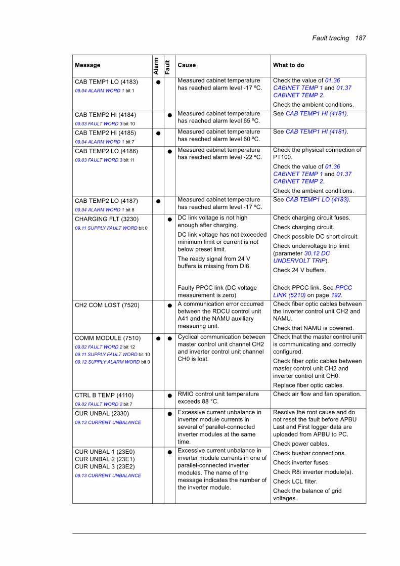
Fault tracing 187
CAB TEMP1 LO (4183)
09.04 ALARM WORD 1 bit 1
Measured cabinet temperature has reached alarm level -17 ºC.
Check the value of 01.36 CABINET TEMP 1 and 01.37 CABINET TEMP 2.
Check the ambient conditions.
CAB TEMP2 HI (4184)
09.03 FAULT WORD 3 bit 10
Measured cabinet temperature has reached alarm level 65 ºC.
See CAB TEMP1 HI (4181).
CAB TEMP2 HI (4185)
09.04 ALARM WORD 1 bit 7
Measured cabinet temperature has reached alarm level 60 ºC.
See CAB TEMP1 HI (4181).
CAB TEMP2 LO (4186)
09.03 FAULT WORD 3 bit 11
Measured cabinet temperature has reached alarm level -22 ºC.
Check the physical connection of PT100.
Check the value of 01.36 CABINET TEMP 1 and 01.37 CABINET TEMP 2.
Check the ambient conditions.
CAB TEMP2 LO (4187)
09.04 ALARM WORD 1 bit 8
Measured cabinet temperature has reached alarm level -17 ºC.
See CAB TEMP1 LO (4183).
CHARGING FLT (3230)
09.11 SUPPLY FAULT WORD bit 0
DC link voltage is not high enough after charging.
DC link voltage has not exceeded minimum limit or current is not below preset limit.
The ready signal from 24 V buffers is missing from DI6.
Check charging circuit fuses.
Check charging circuit.
Check possible DC short circuit.
Check undervoltage trip limit (parameter 30.12 DC UNDERVOLT TRIP).
Check 24 V buffers.
Faulty PPCC link (DC voltage measurement is zero)
Check PPCC link. See PPCC LINK (5210) on page 192.
CH2 COM LOST (7520) A communication error occurred between the RDCU control unit A41 and the NAMU auxiliary measuring unit.
Check fiber optic cables between the inverter control unit CH2 and NAMU.
Check that NAMU is powered.
COMM MODULE (7510)
09.02 FAULT WORD 2 bit 12
09.11 SUPPLY FAULT WORD bit 10
09.12 SUPPLY ALARM WORD bit 0
Cyclical communication between master control unit channel CH2 and inverter control unit channel CH0 is lost.
Check that the master control unit is communicating and correctly configured.
Check fiber optic cables between master control unit CH2 and inverter control unit CH0.
Replace fiber optic cables.
CTRL B TEMP (4110)
09.02 FAULT WORD 2 bit 7
RMIO control unit temperature exceeds 88 °C.
Check air flow and fan operation.
CUR UNBAL (2330)
09.13 CURRENT UNBALANCE
Excessive current unbalance in inverter module currents in several of parallel-connected inverter modules at the same time.
Resolve the root cause and do not reset the fault before APBU Last and First logger data are uploaded from APBU to PC.
Check power cables.
Check busbar connections.
Check inverter fuses.
Check R8i inverter module(s).
Check LCL filter.
Check the balance of grid voltages.
CUR UNBAL 1 (23E0)CUR UNBAL 2 (23E1)CUR UNBAL 3 (23E2)
09.13 CURRENT UNBALANCE
Excessive current unbalance in inverter module currents in one of parallel-connected inverter modules. The name of the message indicates the number of the inverter module.
Message
Ala
rm
Fa
ult Cause What to do

188 Fault tracing
DC OVERVOLT (3210)
09.01 FAULT WORD 1 bit 2
09.11 SUPPLY FAULT WORD bit 15
Excessive DC voltage. This can be caused by
• grid static or transient overvoltages, or
• excessive network voltage during synchronisation.
The default trip limit is 1000 V.
Check level of network voltage, DC voltage and inverter nominal voltage.
Check DC overvoltage trip limit (inverter control program parameter 30.11 DC OVERVOLT TRIP).
DC UNDERVOLT (3220)
09.02 FAULT WORD 2 bit 2
09.11 SUPPLY FAULT WORD bit 14
DC voltage is not sufficient due to missing network phase, blown fuse or internal inverter fault.
Check main and inverter fuses.
Check network voltage.
Check DC undervoltage trip limit (inverter control program parameter 30.12 DC UNDERVOLT TRIP).
DCREF MAX RNG (32AC)
08.06 MPPT STATUS bit 9
MPPT has reached the DC reference maximum range.
Check the settings of parameters 30.05 MPPT DC REF MIN and 30.15 DCREF RANGE ALARM.
DCREF MIN RNG (32AB)
08.06 MPPT STATUS bit 8
MPPT has reached the DC reference minimum range.
Check the settings of parameters 30.05 MPPT DC REF MIN and 30.15 DCREF RANGE ALARM.
DC SWITCH LEV (818C)
Master control program 09.14 PVA FAULT WORD bit 5
09.10 PV FLT ALM WORD bit 3
Voltage difference detected over a closed DC contactor.
Check DC fuses.
Check the DC voltages on both sides of the DC contactor.
DC SWITCH POS (818D)
Master control program 09.14 PVA FAULT WORD bit 6
09.10 PV FLT ALM WORD bit 4
DC contactor status signal does not follow an open/close command
Check DC contactor acknowledgement status is correct in inverter control program parameter 08.05 DI STATUS WORD. Bit2 = K1.1, Bit10 = K1.2, But11 = K1.3, Bit7 = K2.1, Bit8 = K2.2, and Bit12 = K2.3.
Check that the DC contactor follows command signals in inverter control program parameter 01.22 RELAY OUTPUT. Bit2 = K1.1, Bit5 = K1.2, But1 = K1.3, Bit3 = K2.1, Bit4 = K2.2, and Bit6 = K2.3.
DC SWITCH TRP (8188)
Master control program 09.14 PVA FAULT WORD bit 3
09.10 PV FLT ALM WORD bit 1
Tmax type DC breaker has tripped.
Check auxiliary power for DC breaker.
Check that DC breaker DIP breaker is in “AUTO” position.
Check DC breaker trip status. If trip signal is not active, try reclosing the breaker.
DI1 (9081) Fan is not rotating or fan contactor connection is loose. This supervision is valid only when inverter is in RDY_RUN state (ie, parameter 08.01 MAIN STATUS WORD bit 1 = 1).
Check acknowledge circuit connected to digital input DI1 of the inverter control unit.
Check fan. Replace if necessary.
Check +24 V DC circuit connected to digital input DI1 of the inverter control unit. See the circuit diagrams delivered with the inverter.
DI1 (9088)
09.11 SUPPLY FAULT WORD bit 5
09.12 SUPPLY ALARM WORD bit 2
Message
Ala
rm
Fa
ult Cause What to do

Fault tracing 189
EARTH FAULT (2387)
09.12 SUPPLY ALARM WORD bit 13
Programmable fault: Parameter
Ground/Earth fault in grounded/earthed network.
Sum of line currents measured with internal current transducers is too high.
Check main fuses (in case of parallel-connected inverter modules).
Check for earth leakages.
Check power cabling.
Check R8i inverter module(s).
Ground/Earth fault in LCL filter, DC circuit, inverter(s), or current imbalance in parallel-connected inverter modules.
Occurs when APBU-branching unit is not installed to the inverter.
Check busbars.
Check LCL modules.
Earth (ground) fault level too30.02 sensitive.
Check setting of parameter 30.03 EARTH FAULT LEVEL.
EARTH FAULT (2330)
Master control program 09.11 SUPPLY FAULT WORD bit 12
09.01 FAULT WORD 1 bit 4
09.11 SUPPLY FAULT WORD bit 12
Programmable fault: Parameter 30.02
Ground/Earth fault in grounded/earthed network.
Sum of line currents measured with internal current transducers is too high.
Ground/Earth fault in LCL filter, DC circuit, inverter(s), or current imbalance in parallel-connected inverter modules.
Occurs when APBU-branching unit is not installed to the inverter.
Check main fuses (in case of parallel- connected inverter modules).
Check for earth leakages.
Check power cabling.
Check R8i inverter module(s).
Check busbars.
Check LCL modules.
Earth (ground) fault level too sensitive.
Check setting of parameter 30.03 EARTH FAULT LEVEL.
EXT ANALOG IO (7081)
09.04 ALARM WORD 1 bit 10
Analog I/O error on RAIO I/O Extension module.
Check cabinet temperature.
Replace RAIO module if alarm is continuously active.
EXT DIO (7082) Error in the RDIO module or module configuration Contact an ABB service
representative.
EXT EVENT DI4 (9084)
09.11 SUPPLY FAULT WORD bit 4
Programmable fault: Parameter 30.04
Digital input DI4 fault
Note: DI4 is reserved for ground/earth fault monitoring.
Check digital input DI4.
Check setting of parameter 30.04 DI4 EXT EVENT.
EXT EVENT DI5 (9085)
09.11 SUPPLY FAULT WORD bit 2
Programmable fault: Parameters 30.05 and 30.10
Digital input DI5 fault Check digital input DI5.
Check settings of parameters 30.05 DI5 EXT EVENT and 30.10 DI5 TRIP DELAY.
EXT EVENT DI7 (9087)
09.11 SUPPLY FAULT WORD bit 11
Programmable fault: Parameters 30.13 and 30.14
Digital input DI7 (DIIL) fault Check digital input DI7 (DIIL).
Check settings of parameters 30.13 DI7 EXT EVENT and 30.14 DI7 TRIP DELAY.
EXT EVNT DI4 (908B)
09.12 SUPPLY ALARM WORD bit 13
Programmable fault: Parameter 30.04
Digital input DI4 alarm
Note: DI4 is reserved for ground/earth fault monitoring.
Check digital input DI4.
Check setting of parameter 30.04 DI4 EXT EVENT.
Message
Ala
rm
Fa
ult Cause What to do

190 Fault tracing
EXT EVNT DI5 (908C)
09.12 SUPPLY ALARM WORD bit 14
Programmable fault: Parameter 30.05
Digital input DI5 alarm Check digital input DI5.
Check setting of parameter 30.05 DI5 EXT EVENT.
EXT EVNT DI7 (908E)
09.12 SUPPLY ALARM WORD bit 11
Programmable fault: Parameter 30.13
Digital input DI7 (DIIL) alarm Check digital input DI7 (DIIL).
Check setting of parameter 30.13 DI7 EXT EVENT.
FLT (xx)
08.01 MAIN STATUS WORD bit 3
Internal fault Check connections inside inverter cabinet.
Write down the fault code (in brackets). Contact an ABB service representative.
GRID MON ALM (8191)
09.10 PV FLT ALM WORD bit 8
Fault indicated by grid monitoring relay
Check grid condition.
Check grid monitoring relay settings.
Check setting of parameter 39.06 GRIDMON SUPV MODE.
GRID MON FLT (8189)
Master control program 09.14 PVA FAULT WORD bit 4
09.10 PV FLT ALM WORD bit 0
ID N CHANGED (FF68) Inverter ID number has changed from 2 (change is not displayed on control panel).
To change ID number back to 2, go to the Control Unit Selection mode by pressing DRIVE. Press ENTER. Set ID number to 2. Press ENTER.
INT CONFIG (5410) Inverter cannot find all of the configured inverter modules.
Parameters and do not match. Parameter shows the inverter modules found by the RDCU. Parameter determines the amount of inverter modules RDCU should find.
Contact an ABB service representative.
Check the charging circuit AINT, APOW, APBU, and RDCU.
INTERNAL FAULT
09.01 FAULT WORD 1 bit 7
09.11 SUPPLY FAULT WORD bit 8
Internal fault in the inverter unit. Quote exact message from fault log and contact ABB service.
IO FAULT (7000)
09.02 FAULT WORD 2 bit 6
I/O communication fault or error detected on channel CH1 of RDCO module. This can be caused by fault in RDCO module or RMIO control unit or faulty/loose fibre optic cable connection.
Check connections between control unit and RDCO module. Test with new fibre optic cables.
Replace RDCO module / RMIO board.
LOAD FACTORY (FF69) Factory parameter settings are restored.
Wait until restore is completed.
LOST ENERGY (8192)
Master control program 09.15 PVA ALARM WORD bit 5
09.10 PV FLT ALM WORD bit 7
Energy limiting is active (master control program parameter 31.16 POWER LIMITING is set to a value below 100%)
Informative alarm.
LVRT RIDETRGH (32A0) Detected voltage dip in the AC gird. AC voltage is lower than 40.10 LVRT U/Un LEVEL 1.
Alarm is cleared when the AC voltage is greater than 40.10 LVRT U/Un LEVEL 1 + 5%. Check the parameter settings in group 40 LVRT CONTROL.
Message
Ala
rm
Fa
ult Cause What to do

Fault tracing 191
MAIN CNT FLT (FF17)
09.11 SUPPLY FAULT WORD bit 6
Main contactor is not functioning properly, or connection is loose.
The control and feedback signals of the AC contactor do not correspond to each other.
Check AC contactor control circuit wiring.
Check AC contactor operating voltage level.
Check control signals from parameter 01.22 RELAY OUTPUT and corresponding feedback signals from 08.05 DI STATUS WORD.
08.05 DI STATUS WORD : Bit2 = K1.1, Bit10 = K1.2, Bit11 = K1.3, Bit7 = K2.1, Bit8 = K2.2, and Bit12 = K2.3.
01.22 RELAY OUTPUT : Bit2 = K1.1, Bit5 = K1.2, Bit1 = K1.3, Bit3 = K2.1, Bit4 = K2.2, and Bit6 = K2.3.
MOD BOARD T (FF88)
09.03 FAULT WORD 3 bit 14
Overtemperature in AINT board of inverter module.
Check inverter module fan.
Check ambient temperature.
Check AINT board.MOD BOARD T (FF92)
09.04 ALARM WORD 1 bit 14
NET LOST (32A3)
09.12 SUPPLY ALARM WORD bit 10
Network voltage is lost during modulation. Line current is below supervision limit or line frequency differs more than 5 Hz from initial value of 50 or 60 Hz.
Check network conditions (power breaks, voltage transients).
Check network connections.
Check main fuses.
NET VOLT FLT (3100)/(32A2)
09.11 SUPPLY FAULT WORD bit 9
Network voltage is out of acceptable range during grid identification.
Check network voltage.
Restart unit.
NO COMMUNICATION (x) This alarm message is generated by control panel.
- Cabling problem or hardware malfunction detected on panel link.
- If (x) = (4), panel type is not compatible with the inverter program version.
Check panel link connections.
Press RESET key. Reset may take up to half a minute, please wait.
Check panel type and version of the inverter application program (see parameter group 04 INFORMATION). Panel type is printed on panel cover.
OVERCURRENT (2310)
09.01 FAULT WORD 1 bit 1
09.11 SUPPLY FAULT WORD bit 1
09.14 OVERCURRENT FAULT
Excessive inverter module current in several of parallel-connected inverter modules at the same time.
Resolve the root cause and do not reset the fault before APBU Last and First logger data are uploaded from APBU to PC.
Check network voltage.
Check inverter power semiconductors (IGBTs) and current transducers.
Check and analyze data from APBU data logger in case of parallel-connected inverter modules.
OVERCURR 1 (23A0)OVERCURR 2 (23A1)OVERCURR 3 (23A2)
09.14 OVERCURRENT FAULT
Excessive inverter module current in one of parallel-connected inverter modules. The name of the message indicates the number of the inverter module.
Message
Ala
rm
Fa
ult Cause What to do

192 Fault tracing
OVER SWFREQ (FF55)
09.02 FAULT WORD 2 bit 9
Switching overfrequency fault. This may be due to hardware fault in circuit boards.
Replace RMIO board or RDCU control unit.
Replace AINT board.
With parallel connected inverter modules, replace APBU branching unit.
PANEL LOST (5300)
Master control program 09.12 SUPPLY ALARM WORD bit 1
09.12 SUPPLY ALARM WORD bit 1
Local control device (control panel or DriveWindow PC tool) selected as active control location has ceased communicating.
Note: Inverter unit shifts to the remote control mode automatically.
Check control panel and PC connections.
Check control panel connector. See the hardware manual.
Replace control panel.
POWERFAIL (3381)
09.25 POWERFAIL FAULT bit 0
AINT board power loss in the inverter unit (or one of parallel-connected inverter modules).
Check that AINT board power cable is connected.
Check that APOW board is working correctly.
Replace AINT board.
POWERF INV 1 (3382)POWERF INV 2 (3383)POWERF INV 3 (3384)
09.25 POWERFAIL FAULT
The name of the message indicates the number of the inverter module.
PPCC LINK (528C) Occasional runtime communication errors (CRC and 4/5B coding errors) in the link between RDCU control unit and inverter module(s).
Check the fiber optic cables between the RDCU control unit and the inverter module(s) if the alarm is continuously active.
PPCC LINK (5210)
09.02 FAULT WORD 2 bit 11
09.24 PPCC FAULT WORD bit 0
AINT board current measurement fault, or communication fault between control unit and AINT board in the inverter unit (or one of parallel-connected inverter modules).
The fault is activated when charging is completed and the DC voltage is high, but not when DC voltage is disconnected and the control unit has an external power supply.
If the control unit is powered from external supply, ensure that the supply is on.
Check fiber optic cable connection between RDCU control unit and inverter modules.
If the fault persists, replace APBU branching unit, RDCU control unit and inverter AINT board (in this order) until fault disappears.
Faulty power stage. Check the output power semiconductors of the affected inverter module.
PPCC LINK 1 (5280)PPCC LINK 2 (5281)PPCC LINK 3 (5282)
09.24 PPCC FAULT WORD
The name of the message indicates the number of the inverter module.
PVS&PANEL DC (32A8)
Master control program 09.15 PVA ALARM WORD bit 1
09.10 PV FLT ALM WORD bit 9
The inverter DC voltage cannot be controlled to a level close enough to solar panel DC voltage. The DC switch cannot be closed.
At start, check the solar panel and inverter DC voltages (01.01 PV CELL DC and 01.10 DC VOLTAGE respectively).
Compare inverter DC reference range to panel open loop DC voltage (max. 1000 V DC at start).
Message
Ala
rm
Fa
ult Cause What to do

Fault tracing 193
PVS800 TEMP (4294)
Master control program 09.12 SUPPLY ALARM WORD bit 4
09.12 SUPPLY ALARM WORD bit 4
Inverter IGBT temperature is excessive.
Check ambient conditions.
Check air flow and fan operation.
Check heatsink fins for dust pick-up.
Check line current against inverter current.
Check the main circuit for loose connections.
PVS800 TEMP (4210)
09.01 FAULT WORD 1 bit 3
09.11 SUPPLY FAULT WORD bit 0
09.16 OVERTEMP WORD
Inverter module IGBT temperature is excessive.
PVS TEMP 1 U (42A0)PVS TEMP 1 V (42A1)PVS TEMP 1 W (42A2)PVS TEMP 2 U (42A3)PVS TEMP 2 V (42A4)PVS TEMP 2 W (42A5)PVS TEMP 3 U (42A6)PVS TEMP 3 V (42A7)PVS TEMP 3 W (42A8)
09.16 OVERTEMP WORD
The name of the message indicates the number of the inverter module and phase.
QLIM PVS TMP (44A2)
09.12 SUPPLY ALARM WORD bit 8
Inverter temperature is limiting reactive power.
Check ambient conditions.
Check air flow and fan operation.
Check heatsink fins for dust pick-up.
Check line current against inverter nominal current.
RECHARGE ALM (3250)
09.12 SUPPLY ALARM WORD bit 12
DC circuit charging attempted twice within one minute. The charging is delayed to allow the charging resistors to cool down.
Informative alarm.
REPLACE FAN (4280) Running time of inverter module cooling fan has exceeded its estimated life time.
Change fan. Reset fan run time counter. See parameter 01.31 FAN ON-TIME.
REVERSE POW (8187)
Master control program 09.14 PVA FAULT WORD bit 2 (peak)
Master control program 09.14 PVA FAULT WORD bit 7 (level)
09.10 PV FLT ALM WORD bit 0 (peak)
09.10 PV FLT ALM WORD bit 5 (level)
Power flow is from the network towards the solar panels.
Check power flow. If an external DC voltage reference is used, set it to a value lower than the solar generator voltage.
Restart unit.
RT NET LOST (32A1)
09.11 SUPPLY FAULT WORD bit 9
Supply voltage out of RT-area. Check RT area parameters 40.10…40.15.
Missing phase(s) or frequency out of allowed range for 20 seconds during synchronization.
Check network conditions.
Check that the initialized base frequency signal 03.03 or 03.04 is correct.
RUN DISABLED (FFAC)
08.06 MPPT STATUS bit 7
(bit=1 start enable)
09.12 SUPPLY ALARM WORD bit 9
Cut-in conditions are not fulfilled.
24 V missing from DI2 in the inverter control program.
Check the settings of parameters 44.18…44.23.
Message
Ala
rm
Fa
ult Cause What to do

194 Fault tracing
SHORT CIRC (2340)
09.01 FAULT WORD 1 bit 0
09.11 SUPPLY FAULT WORD bit 7
09.15 SHORT CIRC FAULT
Short circuit in several parallel-connected inverter modules at the same time.
Resolve the root cause and do not reset the fault before APBU Last and First logger data are uploaded from APBU to PC.
Measure resistances of inverter power semiconductors (IGBTs).
If faulty IGBTs are found, replace all three IGBT/AGDR packages, AINT and APOW boards and flat cables of the faulted R8i inverter module.
Check main circuit.
SC INV 1 U (23B0)SC INV 1 V (23B1)SC INV 1 W (23B2)SC INV 2 U (23B3)SC INV 2 V (23B4)SC INV 2 W (23B5)SC INV 3 U (23B6)SC INV 3 V (23B7)SC INV 3 W (23B8)
09.15 SHORT CIRC FAULT
Short circuit in one of the parallel-connected inverter modules. The name of the message indicates the number of the inverter module and phase.
SUPPLY PHASE (3130)
09.02 FAULT WORD 2 bit 0
Missing phase during synchronization.
Check main fuses.
Check grid for imbalance.
SYNCHRO FLT (8180) Synchronization to network has failed.
Network frequency has changed considerably since identification routine.
Perform network identification routine again. See parameter 99.07 LINE SIDE ID RUN.
SYSTEM START (1087) Control program is started (control unit is powered).
If this message appears during normal operation, check the 24 V supply to the control unit. Check the wiring for breakages and short circuits.
TEMP DIFF (4380)
09.17 TEMP DIF FLT WORD
09.18 TEMP DIF ALM WORD
Excessive temperature difference between parallel-connected inverter modules.
Excessive temperature can be caused, for example, by unequal current sharing between parallel-connected inverter modules.
Save the User logger from APBU branching unit when the inverter is running.
Check the fans.
Check the air filters.
Check the temperature parameters in group 3.
Check that there are no loose connections.
TEMP DIF 1 U (44B1)TEMP DIF 1 V (44B2)TEMP DIF 1 W (44B3)TEMP DIF 2 U (44B4)TEMP DIF 2 V (44B5)TEMP DIF 2 W (44B6)TEMP DIF 3 U (44B7)TEMP DIF 3 V (44B8)TEMP DIF 3 W (44B9)
09.18 TEMP DIF ALM WORD
Excessive temperature difference between parallel-connected inverter modules. The name of the message indicates the number of the inverter module and phase.
Excessive temperature can be caused, for example, by unequal current sharing between parallel connected inverter modules.
TEMP DIF 1 U (4381)TEMP DIF 1 V (4382)TEMP DIF 1 W (4383)TEMP DIF 2 U (4384)TEMP DIF 2 V (4385)TEMP DIF 2 W (4386)TEMP DIF 3 U (4387)TEMP DIF 3 V (4388)TEMP DIF 3 W (4389)
09.17 TEMP DIF FLT WORD
USER MACRO (FFA1) No User Macro saved or file is defective.
Create User Macro again.
Message
Ala
rm
Fa
ult Cause What to do

Fault tracing 195
List of alarm and fault indications by code>EXT DI4 (1080) . . . . . . . . . . . . . . . . . 181>EXT DI5 (1081) . . . . . . . . . . . . . . . . . 181>EXT DI1 (1082) . . . . . . . . . . . . . . . . . 181>INTERNAL F (1083) . . . . . . . . . . . . . 182SYSTEM START (1087) . . . . . . . . . . . 184SYSTEM START (1087) . . . . . . . . . . . 194>EXT DI1 ALM (1089) . . . . . . . . . . . . . 181>EXT DI4 ALM (108A). . . . . . . . . . . . . 181>EXT DI5 ALM (108B). . . . . . . . . . . . . 181>EXT DI7 ALM (108C) . . . . . . . . . . . . 181DC INPUT DEV (2185) . . . . . . . . . . . . 180OVERCURRENT (2310) . . . . . . . . . . . 191CUR UNBAL (2330) . . . . . . . . . . . . . . 187EARTH FAULT (2330) . . . . . . . . . . . . . 189SHORT CIRC (2340). . . . . . . . . . . . . . 194>OVERCURR (2380) . . . . . . . . . . . . . 183>SHORT CIRC (2381). . . . . . . . . . . . . 184>EARTH FAULT (2383) . . . . . . . . . . . . 180>MAIN CNT F (2384) . . . . . . . . . . . . . 182EARTH FAULT (2387) . . . . . . . . . . . . . 189OVERCURR 1 (23A0) . . . . . . . . . . . . . 191OVERCURR 2 (23A1) . . . . . . . . . . . . . 191OVERCURR 3 (23A2) . . . . . . . . . . . . . 191SC INV 1 U (23B0) . . . . . . . . . . . . . . . 194SC INV 1 V (23B1) . . . . . . . . . . . . . . . 194SC INV 1 W (23B2) . . . . . . . . . . . . . . . 194SC INV 2 U (23B3) . . . . . . . . . . . . . . . 194SC INV 2 V (23B4) . . . . . . . . . . . . . . . 194SC INV 2 W (23B5) . . . . . . . . . . . . . . . 194SC INV 3 U (23B6) . . . . . . . . . . . . . . . 194SC INV 3 V (23B7) . . . . . . . . . . . . . . . 194SC INV 3 W (23B8) . . . . . . . . . . . . . . . 194CUR UNBAL 1 (23E0) . . . . . . . . . . . . . 187CUR UNBAL 2 (23E1) . . . . . . . . . . . . . 187CUR UNBAL 3 (23E2) . . . . . . . . . . . . . 187NET VOLT FLT (3100)/(32A2). . . . . . . 191AC OVERVOLT (3110) . . . . . . . . . . . . 185AC UNDERVOLT (3120) . . . . . . . . . . . 185SUPPLY PHASE (3130) . . . . . . . . . . . 194AC OVERFREQ (3141) . . . . . . . . . . . . 185AC UNDERFREQ (3142) . . . . . . . . . . 185AC OVERVOLT (31A0) . . . . . . . . . . . . 185AC UNDERVOLT (31A1) . . . . . . . . . . . 185AC OVERFREQ (31A2). . . . . . . . . . . . 185AC UNDERFREQ (31A3) . . . . . . . . . . 185DC OVERVOLT (3210) . . . . . . . . . . . . 188DC UNDERVOLT (3220) . . . . . . . . . . . 188CHARGING FLT (3230). . . . . . . . . . . . 187RECHARGE ALM (3250) . . . . . . . . . . 193>DC UNDERVLT (3282) . . . . . . . . . . . 180>CHARGING F (3284) . . . . . . . . . . . . 179>NET VOLT (3285) . . . . . . . . . . . . . . . 183LVRT RIDETRGH (32A0) . . . . . . . . . . 190NET VOLT FLT (3100)/(32A2). . . . . . . 191NET LOST (32A3) . . . . . . . . . . . . . . . . 191>NET LOST (32A6) . . . . . . . . . . . . . . . 183UDC HIGH LIM (32A7) . . . . . . . . . . . . 184PVS&PANEL DC (32A8) . . . . . . . . . . . 192>PVS&PANEL DC (32A9) . . . . . . . . . . 183>RECHARGE ALM (32AA) . . . . . . . . . 184DCREF MIN RNG (32AB) . . . . . . . . . . 188DCREF MAX RNG (32AC) . . . . . . . . . 188>MPPT MIN REF (32AD) . . . . . . . . . . 183>MPPT MAX REF (32AE) . . . . . . . . . . 183DC OVERVOLT (32AF) . . . . . . . . . . . . 180POWERFAIL (3381) . . . . . . . . . . . . . . 192POWERF INV 1 (3382) . . . . . . . . . . . . 192POWERF INV 2 (3383) . . . . . . . . . . . . 192POWERF INV 3 (3384) . . . . . . . . . . . . 192CTRL B TEMP (4110) . . . . . . . . . . . . . 180CTRL B TEMP (4110) . . . . . . . . . . . . . 187CAB TEMP1 HI (4180) . . . . . . . . . . . . 186CAB TEMP1 HI (4181) . . . . . . . . . . . . 186CAB TEMP1 LO (4182) . . . . . . . . . . . . 186CAB TEMP1 LO (4183) . . . . . . . . . . . . 187CAB TEMP2 HI (4184) . . . . . . . . . . . . 187CAB TEMP2 HI (4185) . . . . . . . . . . . . 187CAB TEMP2 LO (4186) . . . . . . . . . . . . 187CAB TEMP2 LO (4187) . . . . . . . . . . . . 187CAB TEMP DIF (4188) . . . . . . . . . . . . 186PVS800 TEMP (4210) . . . . . . . . . . . . . 193REPLACE FAN (4280) . . . . . . . . . . . . 193
>PVS800 TEMP (4291) . . . . . . . . . . . . 183>PVS800 TEMP (4292) . . . . . . . . . . . . 183PVS800 TEMP (4294) . . . . . . . . . . . . . 193PVS TEMP 1 U (42A0) . . . . . . . . . . . . 193PVS TEMP 1 V (42A1). . . . . . . . . . . . . 193PVS TEMP 1 W (42A2) . . . . . . . . . . . . 193PVS TEMP 2 U (42A3) . . . . . . . . . . . . 193PVS TEMP 2 V (42A4). . . . . . . . . . . . . 193PVS TEMP 2 W (42A5) . . . . . . . . . . . . 193PVS TEMP 3 U (42A6) . . . . . . . . . . . . 193PVS TEMP 3 V (42A7). . . . . . . . . . . . . 193PVS TEMP 3 W (42A8) . . . . . . . . . . . . 193TEMP DIFF (4380). . . . . . . . . . . . . . . . 194TEMP DIF 1 U (4381) . . . . . . . . . . . . . 194TEMP DIF 1 V (4382) . . . . . . . . . . . . . 194TEMP DIF 1 W (4383) . . . . . . . . . . . . . 194TEMP DIF 2 U (4384) . . . . . . . . . . . . . 194TEMP DIF 2 V (4385) . . . . . . . . . . . . . 194TEMP DIF 2 W (4386) . . . . . . . . . . . . . 194AIR TEMP 1 (4484) . . . . . . . . . . . . . . . 185AIR TEMP 1 (4484) . . . . . . . . . . . . . . . 185AIR TEMP 2 (4485) . . . . . . . . . . . . . . . 185AIR TEMP 2 (4485) . . . . . . . . . . . . . . . 185AIR TEMP 3 (4486) . . . . . . . . . . . . . . . 185AIR TEMP 3 (4486) . . . . . . . . . . . . . . . 185QLIM PVS TMP (44A2) . . . . . . . . . . . . 193>PLIM EXT TMP (44AB) . . . . . . . . . . . 183>QLIM EXT TMP (44AC) . . . . . . . . . . . 184TEMP DIF 1 U (44B1) . . . . . . . . . . . . . 194TEMP DIF 1 V (44B2) . . . . . . . . . . . . . 194TEMP DIF 1 W (44B3) . . . . . . . . . . . . . 194TEMP DIF 2 U (44B4) . . . . . . . . . . . . . 194TEMP DIF 2 V (44B5) . . . . . . . . . . . . . 194TEMP DIF 2 W (44B6) . . . . . . . . . . . . . 194PPCC LINK (5210). . . . . . . . . . . . . . . . 192PPCC LINK 1 (5280) . . . . . . . . . . . . . . 192PPCC LINK 2 (5281) . . . . . . . . . . . . . . 192PPCC LINK 3 (5282) . . . . . . . . . . . . . . 192PPCC LINK (528C) . . . . . . . . . . . . . . . 192PANEL LOST (5300) . . . . . . . . . . . . . . 183PANEL LOST (5300) . . . . . . . . . . . . . . 192>PANEL LOST (5382) . . . . . . . . . . . . . 183INT CONFIG (5410). . . . . . . . . . . . . . . 190ANALOG IO (5441) . . . . . . . . . . . . . . . 179DIGITAL IO (5442) . . . . . . . . . . . . . . . . 180BATT FAILURE (5581). . . . . . . . . . . . . 186AUTORESET F (6080). . . . . . . . . . . . . 179AUTORESET A (6081) . . . . . . . . . . . . 179RMBA LOST (61A9) . . . . . . . . . . . . . . 184IO START ENA (61AA) . . . . . . . . . . . . 182PARAM CRC (6320) . . . . . . . . . . . . . . 183I/O FAULT (7000) . . . . . . . . . . . . . . . . . 182IO FAULT (7000) . . . . . . . . . . . . . . . . . 190EXT AIO (7081) . . . . . . . . . . . . . . . . . . 181EXT ANALOG IO (7081) . . . . . . . . . . . 189EXT DIO (7082) . . . . . . . . . . . . . . . . . . 181EXT DIO (7082) . . . . . . . . . . . . . . . . . . 189COMM MODULE (7510) . . . . . . . . . . . 180COMM MODULE (7510) . . . . . . . . . . . 187CH2 COM LOSS (7520) . . . . . . . . . . . 180CH2 COM LOST (7520). . . . . . . . . . . . 187>COMM MODULE (7581) . . . . . . . . . . 180>COMM MODULE (758A) . . . . . . . . . . 180ANTI-ISLAND (81A0). . . . . . . . . . . . . . 186>SYNCHRO FLT (8180) . . . . . . . . . . . 184SYNCHRO FLT (8180). . . . . . . . . . . . . 194ISU FAULT (8185) . . . . . . . . . . . . . . . . 182ISU WARNING (8186) . . . . . . . . . . . . . 182>REVERSE POW (8187). . . . . . . . . . . 184REVERSE POW (8187) . . . . . . . . . . . . 193>DC BRK TRP (8188) . . . . . . . . . . . . . 180DC SWITCH TRP (8188) . . . . . . . . . . . 188>GRID MONFLT (8189) . . . . . . . . . . . . 182GRID MON FLT (8189) . . . . . . . . . . . . 190>DC BRK LEV (818C) . . . . . . . . . . . . . 180DC SWITCH LEV (818C) . . . . . . . . . . . 188>DC BRK POS (818D). . . . . . . . . . . . . 180DC SWITCH POS (818D) . . . . . . . . . . 188>BACKPOW LEV (818E) . . . . . . . . . . . 179>QLIM PVS TMP (818F) . . . . . . . . . . . 184>LOST ENERGY (8190) . . . . . . . . . . . 182>GRID MONALM (8191) . . . . . . . . . . . 182
GRID MON ALM (8191) . . . . . . . . . . . .190LOST ENERGY (8192). . . . . . . . . . . . .190ANTI-ISLAND (8193) . . . . . . . . . . . . . .186>RUN DISABLE (8194) . . . . . . . . . . . .184INSUL RESIST (819A) . . . . . . . . . . . . .182GND CLOSE ER (8196) . . . . . . . . . . . .181GND LEAK CUR (8197) . . . . . . . . . . . .182GND HIGH CUR (8198) . . . . . . . . . . . .182GND HIGH VOLT (8199) . . . . . . . . . . .182>ANTI-ISLAND (819F) . . . . . . . . . . . . .179DI1 (9081). . . . . . . . . . . . . . . . . . . . . . .188EXT EVNT DI3 (9083) . . . . . . . . . . . . .181EXT EVNT DI3 (9083) . . . . . . . . . . . . .181EXT EVNT DI4 (9084) . . . . . . . . . . . . .181EXT EVNT DI4 (9084) . . . . . . . . . . . . .181EXT EVENT DI4 (9084) . . . . . . . . . . . .189EXT EVNT DI5 (9085) . . . . . . . . . . . . .181EXT EVNT DI5 (9085) . . . . . . . . . . . . .181EXT EVENT DI5 (9085) . . . . . . . . . . . .189EXT EVENT DI7 (9087) . . . . . . . . . . . .189DI1 (9088). . . . . . . . . . . . . . . . . . . . . . .188EXT EVNT DI4 (908B) . . . . . . . . . . . . .189EXT EVNT DI5 (908C) . . . . . . . . . . . . .190EXT EVNT DI7 (908E) . . . . . . . . . . . . .190EM STOP (F081) . . . . . . . . . . . . . . . . .180EM STOP (F083) . . . . . . . . . . . . . . . . .180MAIN CNT FLT (FF17) . . . . . . . . . . . . .191PVA RUN ENA (FF54) . . . . . . . . . . . . .183OVER SWFREQ (FF55). . . . . . . . . . . .192ILLEGAL INST (FF5F) . . . . . . . . . . . . .182ID N CHANGED (FF68) . . . . . . . . . . . .182ID N CHANGED (FF68) . . . . . . . . . . . .190LOAD FACTORY (FF69) . . . . . . . . . . .182LOAD FACTORY (FF69) . . . . . . . . . . .190MOD BOARD T (FF88) . . . . . . . . . . . .191MOD BOARD T (FF92) . . . . . . . . . . . .191>EXT DI7 (FF96) . . . . . . . . . . . . . . . . .181POWFAIL FILE (FFA0) . . . . . . . . . . . . .183USER MACRO (FFA1) . . . . . . . . . . . . .194BACKUP ERROR (FFA2). . . . . . . . . . .179BACKUP USED (FFA3) . . . . . . . . . . . .179FACTORY FILE (FFA7) . . . . . . . . . . . .181RUN DISABLED (FFAC) . . . . . . . . . . .193APPLIC 1 FLT (FFD6) . . . . . . . . . . . . .179APPLIC 2 FLT (FFD7) . . . . . . . . . . . . .179APP OVERLOAD (FFD9) . . . . . . . . . . .179

196 Fault tracing
Fieldbus control 197
8
Fieldbus control
What this chapter containsThis chapter describes how the PVS800 central inverter can be controlled by external devices over a communication network.
System overviewThe central inverter can be connected to an external control and monitoring system using any of these two methods:• through a communication adapter module connected to the master control unit
or• through NETA-21 connected to channel CH0 and RDCO (DDCS communication
option) module.

198 Fieldbus control
The following diagram shows the control interfaces of the master control unit.
Typically one fieldbus adapter is used at a time. This adapter is installed to SLOT 1 of the RDCU master control unit. The master control unit supports maximum two pieces of R-series fieldbus adapters. If two adapters are used, only RMBA-01 Modbus adapter can be installed to SLOT 2. All other adapters must be installed to SLOT 1.
Commissioning and supporting toolsDriveWindow and other PC tools can be connected to DDCS channel CH3, either in a ring or a star configuration using branching units. Before starting the communication, a unique node address must be set for each connected control unit. See parameter 70.15 CH3 NODE ADDR. The new node address becomes valid on the next power-up of the control unit.
Fieldbus controller
Modbus RTU
Fieldbus adapter Rxxx
Fieldbus adapter RMBA-01
RDCO
SLOT 1
SLOT 2
Other devices
DDCS
PVS800 Master control unit
CH0NETA-21
NEXA-21
Ethernet

Fieldbus control 199
Setting up communication for Modbus RTUThe Modbus RTU can be connected through RMBA-01 Modbus adapter. The RMBA-01 Modbus adapter module is typically installed in SLOT 1 of the master control unit. RMBA-01 can also be installed in SLOT 2 if SLOT 1 is used by any other adapters.
Before configuring the master control program for Modbus RTU control, check that the mechanical and electrical installation of the RMBA-01 Modbus adapter module is according to the instructions in the hardware manual and the adapter module manual.
Set up the Modbus RTU communication by configuring the parameters according to the following list.
Note: If the Modbus RTU interface is used only for direct access to actual signals and parameters (no datasets used), set parameter 98.02 COMM. MODULE to NO.
Parameter Setting Function / information
52.01 STATION NUMBER
According to system setup Defines a node address of the control unit. All devices on the same bus must have unique addresses.
52.02 BAUDRATE According to system setup 1 = 600 bit/s
2 = 1200 bit/s
3 = 2400 bit/s
4 = 4800 bit/s
5 = 9600 bit/s
6 = 19200 bit/s
52.03 PARITY According to system setup 1 = No parity bit, one stop bit
2 = No parity bit, two stop bits
3 = Odd parity indication bit, one stop bit
4 = Even parity indication bit, one stop bit

200 Fieldbus control
Setting up communication for Modbus/TCPThe Modbus/TCP can be connected to the drive through RETA-01 Ethernet adapter module or RETA-02 Ethernet adapter module. The RETA-0x adapter is always installed in SLOT 1 of the master control unit.
Before configuring the master control program for Modbus/TCP connection, check that the mechanical and electrical installation of the adapter module is according to the instructions in the hardware manual and the adapter module manual.
Set up the Modbus/TCP communication by configuring the parameters according to the following list.
If communication settings are changed, reboot the adapter module to apply the changes. You can reboot the adapter module by either setting parameter 51.27 FBA PAR REFRESH to REFRESH or by switching Off/On the auxiliary power of the control unit.
Note: If the Modbus/TCP interface is used only for direct access to actual signals and parameters (no datasets used), set parameter 98.02 COMM. MODULE to NO.
Parameter Setting Function / information
51.03 DHCP Enable According to system setup 0 = DHCP disabled
1 = DHCP enabled
51.04 IP address 1 According to system setup First number of the IP address
51.05 IP address 2 According to system setup Second number of the IP address
51.06 IP address 3 According to system setup Third number of the IP address
51.07 IP address 4 According to system setup Fourth number of the IP address
51.08 Subnet mask 1 According to system setup First number of the subnet mask
51.09 Subnet mask 2 According to system setup Second number of the subnet mask
51.10 Subnet mask 3 According to system setup Third number of the subnet mask
51.11 Subnet mask 4 According to system setup Fourth number of the subnet mask
51.12 GW address 1 According to system setup First number of the gateway address
51.13 GW address 2 According to system setup Second number of the gateway address
51.14 GW address 3 According to system setup Third number of the gateway address
51.15 GW address 4 According to system setup Fourth number of the gateway address
51.16 Protocol Modbus/TCP (0) 0 = Modbus/TCP

Fieldbus control 201
Setting up DDCS communication with NETA-01/-21The inverter can communicate with control and monitoring system using NETA-01/-21 adapters. NETA is connected to master control unit with DDCS fiber optics communication.
To set up communication with NETA-21, define the following parameters. Check also the communication speed for each devices.
Parameter Setting Function / information
70.01 CH0 NODE ADDR Individual address for each control unit connected to NETA-21 starting from 1.
Each device must have a unique node address.
70.03 CH0 BAUD RATE 1 Mb/s Same communication speed must be used in all devices.
70.19 CH0 HW
CONNECTION
According to the connection topology
0 = Ring connection
1 = Star connection

202 Fieldbus control
Cyclical communication with upper control and monitoring system using datasetsInverter parameters can be accessed by reading/writing directly to parameters or by reading/writing parameters through datasets. Datasets provide a way to map different inverter parameters to consecutive addresses and makes communication faster. Each dataset can carry three freely adjustable parameters. If communication timeout monitoring is required, set the parameters in group 70 accordingly.
Set up cyclical communication by defining the following parameters:
Example: Dataset configuration
The parameters used to read and write from or to the inverter through datasets must be defined before using them. See the below example of a dataset configuration.
If parameters 01.10 AC POWER, 01.14 REACTIVE POWER and 01.34 PV MODULE DC MEAS are monitored and parameters 31.16 POWER LIMITING and 24.02 Q POWER REF are used as commands to the inverter, the following dataset configuration can be used:
With this configuration, the following registers can be used from upper control system:
Parameter Setting Function / information
98.02 COMM MODULE ADVANT/N-FB 1 = NO2 = FIELDBUS3 = ADVANT/N-FB4 = STD MODBUS
70.05 CH0 COM LOSS CTRL According to system setup 1 = NO FAULT2 = FAULT
70.04 CH0 TIMEOUT According to system setup This timeout applies to controllers connected to CH0 and R-type fieldbus adapters connected to SLOT1 or SLOT2.
The timeout must be longer than the typical cycle time of the communication.
Parameter Value Description
92.01 D SET 11 VAL 1 110 Maps parameter 01.10 AC POWER into dataset 11, data word 1
92.02 D SET 11 VAL 2 114 Maps parameter 01.14 REACTIVE POWER into dataset 11, data word 2
92.03 D SET 11 VAL 3 134 Maps parameter 01.34 PV MODULE DC MEAS into dataset 11, data word 3
90.01 D SET 10 VAL 1 3116 Maps parameter 31.16 POWER LIMITING into dataset 10, data word 1
90.02 D SET 10 VAL 2 2402 Maps parameter 24.02 Q POWER REF into dataset 10, data word 2
Inverter register Function
31 Reads AC POWER value from inverter
32 Reads REACTIVE POWER value from inverter
33 Reads PV MODULE DC MEAS value from inverter
28 Writes POWER LIMITING value to inverter
29 Writes Q POWER REF value to inverter

Fieldbus control 203
Modbus register addressesThe master control program parameters, data words, references and actual values are mapped into the holding register area. These holding registers can be accessed directly from an external system. There are not setup parameters for mapping the data into the holding register area. The mapping is pre-defined and corresponds directly to the master control program parameter grouping.
The table below shows the parameters and signals of the master control program that can be mapped into the register area:
Dataset mapping
Writing data to the inverter parameters
The table below shows the dataset register addresses used for writing data to the inverter parameters. These registers can be used for writing control, limitation, and reference values to the inverter.
Register area Description
1 … 99 Datasets
101…999 Actual signals 01.01…09.99
1001…9999 Parameters 10.01…99.99
Register address description Configuration parameter
28 dataset 10 data word 1 90.01
29 dataset 10 data word 2 90.02
30 dataset 10 data word 3 90.03
34 dataset 12 data word 1 90.04
35 dataset 12 data word 2 90.05
36 dataset 12 data word 3 90.06
40 dataset 14 data word 1 90.07
41 dataset 14 data word 2 90.08
42 dataset 14 data word 3 90.09
46 dataset 16 data word 1 90.10
47 dataset 16 data word 2 90.11
48 dataset 16 data word 3 90.12
52 dataset 18 data word 1 90.13
53 dataset 18 data word 2 90.14
54 dataset 18 data word 3 90.15
58 Dataset 20 data word 1 90.16
59 Dataset 20 data word 2 90.17
60 Dataset 20 data word 3 90.18
64 dataset 22 data word 1 91.01
65 dataset 22 data word 2 91.02
66 dataset 22 data word 3 91.03
70 Dataset 24 data word 1 91.04
71 Dataset 24 data word 2 91.05
72 Dataset 24 data word 3 91.06

204 Fieldbus control
Reading data from inverter parameters
The table below shows the dataset register addresses used for reading data from inverter parameters.
Register address description Configuration parameter
31 dataset 11 data word 1 92.01
32 dataset 11 data word 2 92.02
33 dataset 11 data word 3 92.03
37 dataset 13 data word 1 92.04
38 dataset 13 data word 2 92.05
39 dataset 13 data word 3 92.06
43 dataset 15 data word 1 92.07
44 dataset 15 data word 2 92.08
45 dataset 15 data word 3 92.09
49 dataset 17 data word 1 92.10
50 dataset 17 data word 2 92.11
51 dataset 17 data word 3 92.12
55 dataset 19 data word 1 92.13
56 dataset 19 data word 2 92.14
57 dataset 19 data word 3 92.15
61 dataset 21 data word 1 92.16
62 dataset 21 data word 2 92.17
63 dataset 21 data word 3 92.18
67 dataset 23 data word 1 93.01
68 dataset 23 data word 2 93.02
69 dataset 23 data word 3 93.03
73 Dataset 25 data word 1 93.04
74 Dataset 25 data word 2 93.05
75 Dataset 25 data word 3 93.06

Fieldbus control 205
Actual signal and parameter mappingActual signals and parameters are mapped in this order: • thousands and hundreds correspond to group number
• tens and ones correspond to the parameter number within a group.
For example, Register = 100 * Group + index
Register address Description
104 Parameter 01.04
3116 Parameter 31.16

206 Fieldbus control

Further informationMore information about ABB products for solar applications on the Internet: www.abb.com/solar

Contact us
www.abb.com/solar
3AUA0000058422 Rev D (EN) 2016-09-23