
Emerging field of few-layered intercalated 2D materials
20
Emerging field of few-layered intercalated 2D materials† Qing Cao, Fabian Grote, Marleen Hubmann and Siegfried Eigler * The chemistry and physics of intercalated layered 2D materials (2DMs) are the focus of this review article. Special attention is given to intercalated bilayer and few-layer systems. Thereby, intercalated few-layers of graphene and transition metal dichalcogenides play the major role; however, also other intercalated 2DMs develop fascinating properties with thinning down. Here, we briefly introduce the historical background of intercalation and explain concepts, which become relevent with intercalating few-layers. Then, we describe various synthetic methods to yield intercalated 2DMs and focus next on current research directions, which are superconductivity, band gap tuning, magnetism, optical properties, energy storage and chemical reactions. We focus on major breakthroughs in all introduced sections and give an outlook to this emerging field of research. 1 Introduction Our mobile and rechargeable world is based on intercalation chemistry. Thus, it is not surprising that the Nobel Prize in Chemistry 2019 was given to the pioneers of the Li-ion battery, Goodenough, Whittingham, and Yoshino. 1 The pioneering work of Whittingham was the report on the reversible interca- lation of layered TiS 2 by Li-ions. The work of Goodenough led to the discovery of layered cobalt oxide as cathode material and the work of Yoshino explored graphite as anode material. Now, energy can be stored by collecting photons from the sun or collecting kinetic energy from wind or water and used at will. With the discovery of graphene by Geim and Novoselov, which was awarded with a Nobel Prize in 2010 it was revealed that properties of materials change with thinning down to the single layer. 2 Thus, novel materials emerged and were studied by physicists. In addition, the chemistry of 2D materials (2DMs) came into the focus of research and new functionalization principles were developed, both of covalent and non-covalent nature. 3–5 Surface physics and surface chemistry, both acceler- ated in recent years and thus, researchers realized that 2DMs properties can be tailored by surface modication, such as the deposition of metal particles or organic donor and acceptor type molecules, respectively. 6,7 In general, countless investigations are being made into the chemistry and physics of 2DMs and a practically innite variety is emerging. Thereby, transition metal dichalcogenides (TMDCs) or 2D allotropes of Si, Bi, P and others possess different band structures. Thus, 2DMs are insulators, topological insulators, semiconductors, conductors, Qing Cao received her MSc from the Institute of Advanced Mate- rials at Nanjing Tech University in 2019. She received her BSc in polymer materials from Shan- dong University of Science and Technology in 2016. She is currently a doctoral candidate in the research group of Prof. Siegfried Eigler at Freie Uni- versit¨ at Berlin. Her research mainly focuses on intercalation and functionalization of 2D materials. Fabian Grote is a doctoral candidate in the group of Prof. Siegfried Eigler at Freie Uni- versit¨ at Berlin. He received his MSc in chemistry from the Julius-Maximilians-Universit¨ at W¨ urzburg in 2019 and his BSc in chemistry from the Friedrich- Alexander-Universit¨ at Erlangen- N¨ urnberg in 2016. His research focuses on the chemistry and fundamental properties of oxo- functionalized graphene. Institute of Chemistry and Biochemistry, Freie Universit¨ at Berlin, Takustrabe 3, 14195 Berlin, Germany. E-mail: [email protected] † Dedicated to Professor Andreas Hirsch on the occasion of his 60th birthday. Cite this: Nanoscale Adv., 2021, 3, 963 Received 25th November 2020 Accepted 31st December 2020 DOI: 10.1039/d0na00987c rsc.li/nanoscale-advances © 2021 The Author(s). Published by the Royal Society of Chemistry Nanoscale Adv., 2021, 3, 963–982 | 963 Nanoscale Advances REVIEW Open Access Article. Published on 15 January 2021. Downloaded on 2/16/2022 2:10:59 PM. This article is licensed under a Creative Commons Attribution 3.0 Unported Licence. View Article Online View Journal | View Issue
Transcript of Emerging field of few-layered intercalated 2D materials
NanoscaleAdvances
REVIEW
Ope
n A
cces
s A
rtic
le. P
ublis
hed
on 1
5 Ja
nuar
y 20
21. D
ownl
oade
d on
2/1
6/20
22 2
:10:
59 P
M.
Thi
s ar
ticle
is li
cens
ed u
nder
a C
reat
ive
Com
mon
s A
ttrib
utio
n 3.
0 U
npor
ted
Lic
ence
.
View Article OnlineView Journal | View Issue
Emerging field o
QtripdTciSvma
materials.
Institute of Chemistry and Biochemistry, Fre
Berlin, Germany. E-mail: siegfried.eigler@fu
† Dedicated to Professor Andreas Hirsch
Cite this: Nanoscale Adv., 2021, 3, 963
Received 25th November 2020Accepted 31st December 2020
DOI: 10.1039/d0na00987c
rsc.li/nanoscale-advances
© 2021 The Author(s). Published by
f few-layered intercalated 2Dmaterials†
Qing Cao, Fabian Grote, Marleen Hubmann and Siegfried Eigler *
The chemistry and physics of intercalated layered 2D materials (2DMs) are the focus of this review article.
Special attention is given to intercalated bilayer and few-layer systems. Thereby, intercalated few-layers of
graphene and transition metal dichalcogenides play the major role; however, also other intercalated 2DMs
develop fascinating properties with thinning down. Here, we briefly introduce the historical background of
intercalation and explain concepts, which become relevent with intercalating few-layers. Then, we describe
various synthetic methods to yield intercalated 2DMs and focus next on current research directions, which
are superconductivity, band gap tuning, magnetism, optical properties, energy storage and chemical
reactions. We focus on major breakthroughs in all introduced sections and give an outlook to this
emerging field of research.
1 Introduction
Our mobile and rechargeable world is based on intercalationchemistry. Thus, it is not surprising that the Nobel Prize inChemistry 2019 was given to the pioneers of the Li-ion battery,Goodenough, Whittingham, and Yoshino.1 The pioneeringwork of Whittingham was the report on the reversible interca-lation of layered TiS2 by Li-ions. The work of Goodenough led tothe discovery of layered cobalt oxide as cathodematerial and thework of Yoshino explored graphite as anode material. Now,energy can be stored by collecting photons from the sun orcollecting kinetic energy from wind or water and used at will.
ing Cao received her MSc fromhe Institute of Advanced Mate-ials at Nanjing Tech Universityn 2019. She received her BSc inolymer materials from Shan-ong University of Science andechnology in 2016. She isurrently a doctoral candidaten the research group of Prof.iegfried Eigler at Freie Uni-ersitat Berlin. Her researchainly focuses on intercalationnd functionalization of 2D
ie Universitat Berlin, Takustrabe 3, 14195
-berlin.de
on the occasion of his 60th birthday.
the Royal Society of Chemistry
With the discovery of graphene by Geim and Novoselov,which was awarded with a Nobel Prize in 2010 it was revealedthat properties of materials change with thinning down to thesingle layer.2 Thus, novel materials emerged and were studiedby physicists. In addition, the chemistry of 2D materials (2DMs)came into the focus of research and new functionalizationprinciples were developed, both of covalent and non-covalentnature.3–5 Surface physics and surface chemistry, both acceler-ated in recent years and thus, researchers realized that 2DMsproperties can be tailored by surface modication, such as thedeposition of metal particles or organic donor and acceptor typemolecules, respectively.6,7 In general, countless investigationsare being made into the chemistry and physics of 2DMs anda practically innite variety is emerging. Thereby, transitionmetal dichalcogenides (TMDCs) or 2D allotropes of Si, Bi, P andothers possess different band structures. Thus, 2DMs areinsulators, topological insulators, semiconductors, conductors,
Fabian Grote is a doctoralcandidate in the group of Prof.Siegfried Eigler at Freie Uni-versitat Berlin. He received hisMSc in chemistry from theJulius-Maximilians-UniversitatWurzburg in 2019 and his BSc inchemistry from the Friedrich-Alexander-Universitat Erlangen-Nurnberg in 2016. His researchfocuses on the chemistry andfundamental properties of oxo-functionalized graphene.
Nanoscale Adv., 2021, 3, 963–982 | 963
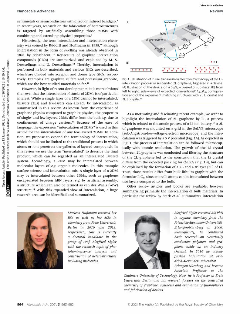
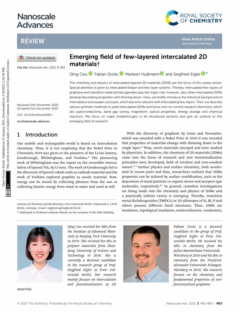
Fig. 1 Illustration of in situ transmission electronmicroscopy of the Li-intercalation process in suspended 2L graphene, triggered in a device.(A) Illustration of the device on a Si3N4-covered Si substrate. (B) fromleft to right: side-views of expected ‘conventional’ C6LiC6 configura-tion and of the experiment matching structures with 2L Li crystal and3L Li crystal.15
Nanoscale Advances Review
Ope
n A
cces
s A
rtic
le. P
ublis
hed
on 1
5 Ja
nuar
y 20
21. D
ownl
oade
d on
2/1
6/20
22 2
:10:
59 P
M.
Thi
s ar
ticle
is li
cens
ed u
nder
a C
reat
ive
Com
mon
s A
ttrib
utio
n 3.
0 U
npor
ted
Lic
ence
.View Article Online
semimetals or semiconductors with direct or indirect bandgap.8
In recent years, research on the fabrication of heterostructuresis targeted by articially assembling those 2DMs withcombining and extending physical properties.9
Historically, the term intercalation and intercalation chem-istry was coined by Rudorff and Hoffmann in 1938,10 althoughintercalation in the form of swelling was already observed in1841 by Schaaeutl.11 Key-results of graphite intercalationcompounds (GICs) are summarized and explained by M. S.Dresselhaus and G. Dresselhaus.12 Thereby, intercalation isperformed in bulk materials and various GICs are described,which are divided into acceptor and donor type GICs, respec-tively. Examples are graphite sulfate and potassium graphite,which are the best studied materials so far.12
However, in light of recent developments, it is more obviousthan ever that the intercalation of stacks of 2DMs is of particularinterest. While a single layer of a 2DM cannot be intercalated,bilayers (2Ls) and few-layers can already be intercalated, assummarized in this review. As known from the experience ofgraphene physics compared to graphite physics, the propertiesof single- and few-layered 2DMs differ from the bulk e.g. due toconnement of charge carriers.13 Because of the ease oflanguage, the expression “intercalation of 2DMs” is used in thisarticle for the intercalation of any few-layered 2DMs. In addi-tion, we propose to expand the terminology of intercalation,which should not be limited to the traditional process in whichatoms or ions penetrate the galleries of layered compounds. Inthis review we use the term “intercalated” to describe the nalproduct, which can be regarded as an intercalated layeredsystem. Accordingly, a 2DM may be intercalated betweenmolecular layers of e.g. organic molecules. In this examplesurface science and intercalation mix. A single layer of a 2DMmay be intercalated between other 2DMs, such as grapheneencapsulated between hBN layers, e.g. by articial assembly,a structure which can also be termed as van der Waals (vdW)structure.14 With this expanded view of intercalation, a hugeresearch area can be identied and summarized.
Marleen Hubmann received herBSc as well as her MSc inchemistry from Freie UniversitatBerlin in 2016 and 2019,respectively. She is currentlya doctoral candidate in thegroup of Prof. Siegfried Eiglerwith the research topic of pho-toluminescence analysis andconstruction of heterostructuresincluding molecules.
964 | Nanoscale Adv., 2021, 3, 963–982
As a motivating and fascinating recent example, we want tohighlight the intercalation of 2L graphene by Li, a processwhich is related to the anode process of a Li-ion battery.15 A 2Lof graphene was mounted on a grid in the SALVE microscope(sub-Angstrom-low-voltage-electron microscope) and the inter-calation was triggered by a 5 V potential (Fig. 1A). As depicted inFig. 1, the process of intercalation can be followed microscop-ically with atomic resolution. The growth of the Li crystalbetween 2L graphene was conducted and ltering the structureof the 2L graphene led to the conclusion that the Li crystaldiffers from the expected packing for C6LiC6 (Fig. 1B), but canbe explained by the formation of a 2L and a trilayer (3L) of Li.Thus, those results differ from bulk lithium graphite with theformular LiC6, since more Li atoms can be intercalated betweentwo layers compared to the bulk.
Other review articles and books are available, howeversummarizing primarily the intercalation of bulk materials. Inparticular the review by Stark et al. summarizes intercalation
Siegfried Eigler received his PhDin organic chemistry from theFriedrich-Alexander-UniversitatErlangen-Nurnberg in 2006.Subsequently, he conductedbasic research on electricallyconductive polymers and gra-phene oxide as an industrychemist. In 2016 he accom-plished habilitation at Frie-drich-Alexander-UniversitatErlangen-Nurnberg and becameAssociate Professor at the
Chalmers University of Technology. Now, he is Professor at FreieUniversitat Berlin and his research focuses on the controlledchemistry of graphene, synthesis and evaluation of uorophoresand fabrication of devices.
© 2021 The Author(s). Published by the Royal Society of Chemistry
Fig. 3 Concept of few-layer surface functionalization/intercalation.(A) Surface functionalized few-layer material, here the interior 2L differfrom the outer layers; (B) as in (A), but with substrate influence leadingto Janus-type properties; (C) few-layered material with intercalationonly on the top; (D) and (E) illustration of stage 2 and stage 20 inter-calation for 3L materials.
Review Nanoscale Advances
Ope
n A
cces
s A
rtic
le. P
ublis
hed
on 1
5 Ja
nuar
y 20
21. D
ownl
oade
d on
2/1
6/20
22 2
:10:
59 P
M.
Thi
s ar
ticle
is li
cens
ed u
nder
a C
reat
ive
Com
mon
s A
ttrib
utio
n 3.
0 U
npor
ted
Lic
ence
.View Article Online
processes not only on bulk, but also 2D level.12,16–20 Thus, herewe keep history and bulk information short, since it is coveredin the above mentioned articles. Further, we introduce impor-tant principles relevant for few-layer, trilayer (3L), bilayer (2L)and monolayer (1L) intercalation. Moreover, we highlight therecent advances. More specically, we will focus on concepts,the synthetic access to intercalated 2DMs and introducecommon methods, such as vapor transport, solvent based orelectrochemical methods and articial assembly. Next, wehighlight recent results and properties of intercalated 2DMsystems.
2 Concept of staging
Here, we introduce concepts and denitions relevant for 2DMsintercalation, which are derived from denitions introduced forGICs. We note that the historical background and intercalationconcepts for bulk materials are summarized in the excellentperspective article of Lerf.20 In particular, staging and chargetransfer are of importance to describe the structure and prop-erties of intercalation compounds. With thinning down thebulk to the 1L additional considerations become important,which are bridging intercalation and surface science.
2.1 Staging in bulk materials
As depicted in Fig. 2A surface functionalization differs fromintercalation. The most important concept for describingintercalated materials is staging, which is used to describe thestructure of layered materials with guest atoms, ions or mole-cules. This concept is best studied for GICs. Accordingly, stage nwas dened with n as number of layers. Thus, if we dene A asmaterials layer and B as intercalant layer, stage 1 possesses anABABAB sequence (Fig. 2B), stage 2 AABAABAAB sequence(Fig. 2C), stage 3 AAABAAAB sequence etc.
However, also mixed systems are possible with e.g. partially-lled layers, in particular occurring for natural systems, asa consequence of the kinetic control of intercalation (Fig. 2D). Itis obvious that a small intercalant must enter the galleries ofa layered bulk material from the side and intercalation startsfrom all rims at the same time. However, for the example ofa stage 2 compound the hypothetical le rim intercalant does
Fig. 2 Concept of bulk surface functionalization/intercalation. (A)Layered bulk material with surface functionalization; the interior is notinfluenced; (B) stage 1 intercalation compound; (C) stage 2 intercala-tion compound; (D) irregular, ill-defined stage 2 intercalationcompound.
© 2021 The Author(s). Published by the Royal Society of Chemistry
not know at which layer the intercalant on the right rim starts.Such a mismatch cannot be corrected and will consequentlylead to a mixed layer sequence. For a 2L material there is onlyone gallery to be intercalated. With the given examples, thedifference between surface manipulation, by interacting mole-cules or atoms, and intercalation becomes clear, since withintercalation layers, the bulk can be inuenced from inside.With thinning the layered materials, the surface becomes moreimportant for manipulating materials properties and thus,interesting effects emerge as outlined in the next chapters.
2.2 From bulk to few-layers of intercalated 2D materials
Few-layered 2DMs are obtained at rst sight with thinningdown from bulk.21 However, the concept of staging loses itsvalidity with reaching 1L, instead surface science describes thesystems. Here, we introduce some of the possible structures forfew-layered systems, followed by three, two and one layers of2DMs (Fig. 3 and 4).
As shown in Fig. 3A the four layers (4L) are an example ofa few-layered material with the surface inuenced by moleculesor atoms. In that example with 4L the orange marked layers canbe distinguished from the inner black marked layers and thereis consequently a junction between orange and black layers.However, for more than roughly six layers surface functionali-zation does not play a crucial role for the interior layers, sincethe proportion of surface layers to the interior layers becomesminor.
Fig. 4 Suspended 3L, 2L and 1L materials with surface functionaliza-tion/intercalation. (A) 3L stage 20 intercalated and bottom surfacefunctionalization; (B) surface functionalized suspended 2L; (C) Janus-type surface functionalized 2L; (D) 1L material intercalated betweenmolecular layers; (E) Janus-type suspended 1L material; (D) and (E)could be considered as 2D 1L intercalated between molecular layers.
Nanoscale Adv., 2021, 3, 963–982 | 965

Fig. 5 Study of device-based electrochemical intercalation of Li inheterostructures of (A) graphene (G) artificially intercalated in hBN and(B) 2L graphene artificially intercalated in hBN.
Fig. 6 Two-zone thermal transport for potassium into graphite andstage control by temperature difference. Reproduced from ref. 16 with
Nanoscale Advances Review
Ope
n A
cces
s A
rtic
le. P
ublis
hed
on 1
5 Ja
nuar
y 20
21. D
ownl
oade
d on
2/1
6/20
22 2
:10:
59 P
M.
Thi
s ar
ticle
is li
cens
ed u
nder
a C
reat
ive
Com
mon
s A
ttrib
utio
n 3.
0 U
npor
ted
Lic
ence
.View Article Online
Even for the example of 4Ls the substrate plays an importantrole. As illustrated in Fig. 3B and C, with consideringa substrate, Janus-type functionalization (different functional-ities on two sides) is realized no matter whether atoms ormolecules are placed between the substrate and the 2DM or not.For the 3L examples in Fig. 3D and E the concept of staging isadopted, here, with stage 2 as an example. Starting with a 3L ona substrate and an intercalant preferring stage 2 formation, twodifferent congurations can be considered, and thus, eithera 1L or 2L is on the substrate. Here, we introduce stage 2 andstage 20, respectively, to differentiate between those two cases.The example in Fig. 3D starts from the top like a stage 2compound. Thus, we assign stage 20 to the example in Fig. 3E.
In Fig. 4A a stage 20 structure is shown, however, in contrastto Fig. 3E the structure is suspended, which can be realized byplacing the structure on top of a hole in the substrate. A similarstructure is shown in Fig. 1A for a 2L of graphene. In general,with suspending few-layered 2DMs transmission is possible,however, also surface manipulation, such as doping becomespossible accounting for different surfaces. This is the pointwhere surface science plays the decisive role in manipulating2DMs. For a 2L both surfaces can be accessed by molecules oratoms, which are the same (Fig. 4B) or different ones (Fig. 4C);the latter leading to Janus-type functionalization. Taking theconcept of staging into account a stage 2 conguration can berealized for a 2L, although no intercalation occurs. For a 1Lsimilar surface functionalization is possible, as shown inFig. 4D and E. In those examples, the 1L is however intercalatedbetween molecular layers and thus, surface science and inter-calation chemistry merge.
In a recent study, intercalation of vdW heterostructures ofgraphene and 2L graphene, respectively, was studied in anelectrochemical device (as outlined in chapter 3).22 The struc-tures prepared are illustrated in Fig. 5A and B. As shown inFig. 5A intercalation proceeds at the interface between hBN andgraphene, on both sides. However, the properties differ frompure surface functionalization or a stage 1 bulk intercalationcompound, due to the interaction of Li and hBN (about 30L oneach side). The authors conclude that Li is randomly distrib-uted, and the amount of Li atoms is signicantly lowercompared to the bulk with carrier densities of about 7 � 1013
cm�2, corresponding to a stoichiometry of LiC60.In contrast, a 2L of graphene intercalated in hBN, as shown
in Fig. 5B, behaves differently because intercalation of the 2Lallows a much higher loading compared to the graphene/hBN
966 | Nanoscale Adv., 2021, 3, 963–982
interface. Here, the carrier density was determined to 5.5 �1014 cm�2, with a contribution of 4.6 � 1014 cm�2 for thegraphene/graphene interface.
2.3 Considerations on geometry and charge carrier densities
When approaching a 1L of a 2DM, or by stacking few-layers of2DMs on top of each other or by intercalating materials, atomic-scale illustrations become important to imagine the dimen-sions. In this regard, structures are oen evaluated by transportmeasurements in devices. As a result, the mobility of chargecarriers is determined, either in eld effect transistors or inmagnetic elds by Hall-bar measurements. Finally, taking thedimensions of the device into account a charge carrier density isderived with the unit cm�2 for 2DMs. However, for an atomicimagination the unit cell dimensions are important to take intoaccount. For graphene, the unit cell contains two carbon atoms,with two equal lattice vectors. The calculated area for onecarbon atom is 0.026195 nm2 or 0.026195 � 10�14 cm2 (order ofmagnitude comparable to typical charge carrier densities),respectively.23 This means that there are 38 � 1014 C-atoms percm2. For the example illustrated in Fig. 5, this considerationmeans that there is one charge on about 14 C-atoms, taking the2L structure and interaction of all intercalated Li-atoms intoaccount.
For MoS2 the area of the unit cell is 0.088 nm2 including oneMo and two S atoms, of which one points up and one down.Accordingly, there are 11 � 1014 Mo-atoms per cm2 and 22 �1014 S-atoms per cm2. In another example the intercalatedheterostructure MoS2/Li/graphene was analyzed by densityfunctional theory calculations,24 with a charge carrier density of3.6 � 1014 cm�2 for graphene and 6.0 � 1014 cm�2 for MoS2.According to the considerations above those value relate to onecharge carrier on about 10.6 C-atoms and 3.7 S-atoms,respectively.
permission from Wiley-VCH Verlag GmbH & Co, Copyright 2019.
© 2021 The Author(s). Published by the Royal Society of Chemistry
Review Nanoscale Advances
Ope
n A
cces
s A
rtic
le. P
ublis
hed
on 1
5 Ja
nuar
y 20
21. D
ownl
oade
d on
2/1
6/20
22 2
:10:
59 P
M.
Thi
s ar
ticle
is li
cens
ed u
nder
a C
reat
ive
Com
mon
s A
ttrib
utio
n 3.
0 U
npor
ted
Lic
ence
.View Article Online
3 Synthetic access to intercalated 2Dmaterials3.1 Intercalation by vapor-transport
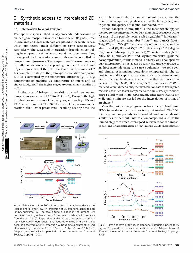
The vapor transport method usually proceeds under vacuum oran inert gas atmosphere in a sealed two-zone cell (Fig. 6A).12 Theintercalants and host materials are placed in separate zones,which are heated under different or same temperatures,respectively. The success of intercalation depends on control-ling the temperature of the host zone and intercalant zone. Also,the stage of the intercalation compounds can be controlled bytemperature adjustments. The temperature of the two zones canbe different or isotherm, depending on the chemical andphysical properties of the intercalant and the host material.25
For example, the stage of the prototype intercalation compoundK-GICs is controlled by the temperature difference Tg � Ti (Tg:temperature of graphite; Ti: temperature of intercalant) asshown in Fig. 6B.26 The higher stages are formed at a smaller Tg� Ti.
In the case of halogen intercalation, typical preparationtemperatures are around 20 �C to 60 �C for Tg. Owing to the highthreshold vapor pressure of the halogens, such as Br2,27 IBr andICl, Ti is set from �30 �C to 60 �C to control the pressure in thereaction cell.28 Other parameters, including heating time, the
Fig. 7 Fabrication of an FeCl3 intercalated 2L graphene device. (A)Pristine and (B) after FeCl3 intercalation of 2L graphene deposited onSi/SiO2 substrate. (A0) The sealed tube is placed in the furnace. (B0)Sufficient washing with acetone (C) removes the adsorbed moleculesfrom the surface. (D) Deposition of electrodes using standard lithog-raphy fabrication techniques. (E) Gradual downshifts of the Raman Gpeaks is observed (after intercalation without air exposure; blue) andafter washing in acetone for 0, 0.16, 0.5, 1 (black), and 12 h (red).Adapted from ref. 47 with permission from the American ChemicalSociety, Copyright 2011.
© 2021 The Author(s). Published by the Royal Society of Chemistry
size of host materials, the amount of intercalant, and thevolume and shape of ampoule also affect the homogeneity andin general the quality of the nal compound.12,29,30
Vapor transport intercalation is the most widely appliedmethod for the intercalation of bulk materials, because it worksfor most of the possible hosts, such as graphite,12 fullerenes,31
single-walled carbon nanotubes,32 hBN33 and TMDCs (MoS2,TaS2, WS2 and WSe2)34–36 and a variety of intercalants, such asalkali metal (K, Rb and Cs)26,37,38 or their alloys,39,40 halogens(Br2)27 or interhalogens (IBr and ICl),28,41 metal halides (FeCl3,AlCl3, SbCl5 and AsF5)42–45 and organic molecules (pyridine,cyclopropylamine).46 This method is already well developed forbulk intercalation. Thus, it can be easily and directly applied to2D host materials using the same equipment (two-zone cell)and similar experimental conditions (temperature). The 2Dhost is normally deposited on a substrate or a manufactureddevice that can be directly inserted into the reaction cell, asdepicted in Fig. 7A–D, illustrating FeCl3 intercalation.47 Withreduced lateral dimensions, the intercalation rate of few-layeredmaterials is much faster compared to the bulk. The synthesis ofstage 1 alkali metal (K, Rb) GICs usually takes more than 12 h,48
while only 5 min are needed for the intercalation of 1–15L ofgraphene.49
Over the past decade, progress has been made in few-layered2DMs intercalation by the vapor transport method. The 2DMintercalation compounds were studied and some showedsimilarities to their bulk intercalation compound, such as theformed stage,49,50 which offers good references for the investi-gation and characterization of few-layered 2DMs intercalation.
Fig. 8 Raman spectra of few layer graphene materials exposed to (A)Br2 and (B) I2 and the derived intercalation models. Adapted from ref.50 with permission from the American Chemical Society, Copyright2009.
Nanoscale Adv., 2021, 3, 963–982 | 967
Nanoscale Advances Review
Ope
n A
cces
s A
rtic
le. P
ublis
hed
on 1
5 Ja
nuar
y 20
21. D
ownl
oade
d on
2/1
6/20
22 2
:10:
59 P
M.
Thi
s ar
ticle
is li
cens
ed u
nder
a C
reat
ive
Com
mon
s A
ttrib
utio
n 3.
0 U
npor
ted
Lic
ence
.View Article Online
For few-layered 2DMs the effect of surface adsorption of inter-calants becomes non-negligible as discussed in chapter 2. Forexample, Br2 and I2 have been attempted to intercalate inmechanically exfoliated 1–4L of graphene on a p-type Si/SiO2
wafer.50,51 The wafer with host materials was placed in one zoneof a glass cell, while liquid halogen was placed in another zoneat a temperature of 10 �C to keep a constant vapor pressure inthe cell. To avoid any impurities, the tube cell was initiallyevacuated to 2.7� 10�5 mbar and the liquid halogen was frozenand thawed several times to remove dissolved gases. Aer 1 h ofBr2 exposure, Br2 was successfully intercalated into 3L and 4L ofgraphene, respectively. In contrast, for 2L and 1L graphene, Br2was symmetrically adsorbed on the top and bottom surfaces.Those results are consistent with the observations made for theBr2-GIC, with stage 2 as the lowest reported stage.27 Accordingly,the model as shown in Fig. 8A is concluded from Raman spectraof the intercalation compounds. A single G peak near 1612 cm�1
is found for 2L and 4L graphene, which are symmetricallyintercalated and doped, similar to the bulk Br2-GIC reference.However, the 1L showed an upshi of the G peak to 1614 cm�1,which relates to a higher charge carrier concentration for thesingle graphene layer. For intercalated 3L graphene, two Gpeaks are detected, which indicates two different types ofinequivalent graphene layers as a result of asymmetricintercalation.
Few-layer graphene was also exposed to I2. Raman spectra for3L and more layers treated with I2 showed two G peaks (Fig. 8B).This means I2 adsorbs only on the top and the bottom of few-layer graphene without intercalation, possibly because thelonger I2 bond length does not allow an intercalation struc-ture.52 Similar to bulk intercalation, Br2 is also the only diatomicnonpolar halogen molecule that can be easily intercalated intographite. However, iodine in interhalogen compounds such asICl and IBr can be intercalated.53
Compared to alkali metal intercalation compounds, it is re-ported that FeCl3 intercalation compounds are relatively stableat ambient conditions.54 Those materials can be safely removed
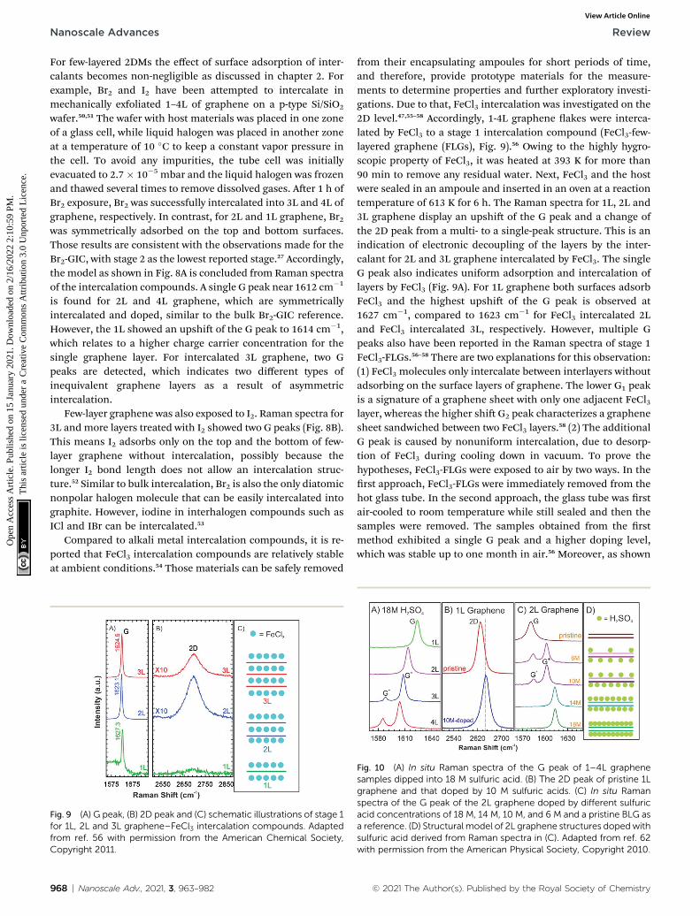
Fig. 9 (A) G peak, (B) 2D peak and (C) schematic illustrations of stage 1for 1L, 2L and 3L graphene–FeCl3 intercalation compounds. Adaptedfrom ref. 56 with permission from the American Chemical Society,Copyright 2011.
968 | Nanoscale Adv., 2021, 3, 963–982
from their encapsulating ampoules for short periods of time,and therefore, provide prototype materials for the measure-ments to determine properties and further exploratory investi-gations. Due to that, FeCl3 intercalation was investigated on the2D level.47,55–58 Accordingly, 1-4L graphene akes were interca-lated by FeCl3 to a stage 1 intercalation compound (FeCl3-few-layered graphene (FLGs), Fig. 9).56 Owing to the highly hygro-scopic property of FeCl3, it was heated at 393 K for more than90 min to remove any residual water. Next, FeCl3 and the hostwere sealed in an ampoule and inserted in an oven at a reactiontemperature of 613 K for 6 h. The Raman spectra for 1L, 2L and3L graphene display an upshi of the G peak and a change ofthe 2D peak from a multi- to a single-peak structure. This is anindication of electronic decoupling of the layers by the inter-calant for 2L and 3L graphene intercalated by FeCl3. The singleG peak also indicates uniform adsorption and intercalation oflayers by FeCl3 (Fig. 9A). For 1L graphene both surfaces adsorbFeCl3 and the highest upshi of the G peak is observed at1627 cm�1, compared to 1623 cm�1 for FeCl3 intercalated 2Land FeCl3 intercalated 3L, respectively. However, multiple Gpeaks also have been reported in the Raman spectra of stage 1FeCl3-FLGs.56–58 There are two explanations for this observation:(1) FeCl3 molecules only intercalate between interlayers withoutadsorbing on the surface layers of graphene. The lower G1 peakis a signature of a graphene sheet with only one adjacent FeCl3layer, whereas the higher shi G2 peak characterizes a graphenesheet sandwiched between two FeCl3 layers.58 (2) The additionalG peak is caused by nonuniform intercalation, due to desorp-tion of FeCl3 during cooling down in vacuum. To prove thehypotheses, FeCl3-FLGs were exposed to air by two ways. In therst approach, FeCl3-FLGs were immediately removed from thehot glass tube. In the second approach, the glass tube was rstair-cooled to room temperature while still sealed and then thesamples were removed. The samples obtained from the rstmethod exhibited a single G peak and a higher doping level,which was stable up to one month in air.56 Moreover, as shown
Fig. 10 (A) In situ Raman spectra of the G peak of 1–4L graphenesamples dipped into 18 M sulfuric acid. (B) The 2D peak of pristine 1Lgraphene and that doped by 10 M sulfuric acids. (C) In situ Ramanspectra of the G peak of the 2L graphene doped by different sulfuricacid concentrations of 18 M, 14 M, 10 M, and 6 M and a pristine BLG asa reference. (D) Structural model of 2L graphene structures dopedwithsulfuric acid derived from Raman spectra in (C). Adapted from ref. 62with permission from the American Physical Society, Copyright 2010.
© 2021 The Author(s). Published by the Royal Society of Chemistry
Fig. 11 Intercalation of (A and B) single and multiple (C) zero-valentmetal atoms into Bi2Se3. Adapted from ref. 66 with permission fromthe American Chemical Society, Copyright 2015. (D) Schematic illus-tration of seamlessly integrated n-type SnS2, p-type Cu–SnS2 andmetallic Co–SnS2 within a single nanosheet. (E) Schematics of thespatially controlled intercalation process for 2L SnS2.67
Review Nanoscale Advances
Ope
n A
cces
s A
rtic
le. P
ublis
hed
on 1
5 Ja
nuar
y 20
21. D
ownl
oade
d on
2/1
6/20
22 2
:10:
59 P
M.
Thi
s ar
ticle
is li
cens
ed u
nder
a C
reat
ive
Com
mon
s A
ttrib
utio
n 3.
0 U
npor
ted
Lic
ence
.View Article Online
in Fig. 7B and C, adsorbed FeCl3 on graphene surface can besimply removed by washing in acetone. According to the Ramanspectrum, the G peak shis down continuously with increasedwashing time. Finally, a 1L is recovered with a normal G peakposition, which decreased to �1580 cm�1, while the G peak of2L graphene did not shi back to the undoped value (Fig. 7E).This difference indicates that the intercalated molecules aremore stable owing to the protection between graphene layers,but would be eventually deintercalated by more extensiverinsing in acetone or other solvents such as hydrochloric acid.47
Through vapor transport intercalation, a lot of intercalantand host pairs have been fabricated on the bulk level (asmentioned above), but only few are reported for few-layered
Table 1 Summary of reactions to generate zerovalent species, and pAmerican Chemical Society, Copyright 2012a
Intercalant Precursor(s)
Copper Tetrakis (acetonitrile) copper(I) hexauorophoSilver Silver nitrate; 0.1 g 5,5,7,12,12,14-hexamethyl
tetraazocyclotetradecaneTin Stannous chloride; 0.1 g tartaric acidGold Gold(I) chloride or chlorotristriphenylphosphIndium Indium(I) chlorideCobalt Dicobalt octacarbonylIron Iron pentacarbonylNickel Nickel(II) nitrate pentahydrate; hydrazine hyd
a 1L ¼ tetraazocyclic amine ligand.
© 2021 The Author(s). Published by the Royal Society of Chemistry
2DMs. As the vapor transport method can directly be appliedfor few-layered 2DMs intercalation, more intercalants and hostmaterials can be investigated in the future. However, theinstability of the intercalation compounds hampers the real-time characterization and thus, also limits furtherinvestigations.
3.2 Solvent-based intercalation
Nonelectrochemical solvent-based intercalation is easy to apply,compared to other methods, since no special equipment orreaction conditions are necessary. Typically, the host material issoaked in a solution of the intercalant. The intercalationprocess is oen accompanied by chemical reactions, enablingintercalation or post reactions. The most representativeexample is the synthesis of graphite oxide by Hummersmethod.59 In the rst step, graphite is dispersed in sulfuric acidwith an oxidant to form graphite sulfate, an intercalationcompound with the stoichiometry [C24
+HSO4�$2H2SO4]n.10,60
During this process the oxidant p-dopes graphite enablingintercalation of hydrogensulfate counterions and sulfuric acidmolecules.61 With adding more oxidant, such as potassiumpermanganate further chemical modications occur on bothsides of the interlayers and nally covalent C–O bonds areformed. In this way, graphite oxide is formed, which can bedelaminated to graphene oxide.3
Nevertheless, in the absence of oxidizing agents, this reac-tion works differently for 1–4L of graphene hosts, for whichsulfuric acid molecules are found to be only physically adsorbedon the top and bottom layers without intercalation.62 The Gpeaks of 1–4L of graphene in 18 M sulfuric acid show similarRaman spectra as observed for graphene few-layers withadsorbed I2, although the chemical doping of I2 vapours ongraphene is quite different (Fig. 8B and 10A). The 2D peak of 1Lgraphene upshis by about 10 cm�1 aer dipping into 10 Msulfuric acid, as shown in Fig. 10B, which is a typical charac-teristic of hole doping in graphene layers.63 As shown in Fig. 10Cand D, the doping level of the top and bottom graphene layerscan be asymmetric by adjusting the concentration of sulfuricacid to 6 M and 10 M, respectively. At a low concentration ofsulfuric acid, the molecules are not completely adsorbed on the
recursor chemistry. Adapted with permission from ref. 64 from the
Reaction
sphate 2Cu(aq)+ / Cu(aq)
2+ + Cu(0)-1,4,8,11- 2Ag+ + L / AgL2+ + Ag(0)
2Sn2+ / Sn4+ + Sn(0)ine gold(I) 3Au(aq)
+ / Au(aq)3+ + 2Au(0)
3InCl 4 InCl3 + 2In(0)Co2(CO)8 / 8CO + 2Co(0)Fe(CO)5 / 5CO + Fe (0)
rate 2Ni2+ + N2H4 + 4OH� / 2Ni(0) + N2 + 4H2O
Nanoscale Adv., 2021, 3, 963–982 | 969
Fig. 12 Configuration of an electrochemical cell for bulk intercalationand typical reactions as well as typical intercalants. Reproduced fromref. 81 with permission fromWiley-VCH Verlag GmbH & Co, Copyright2020.
Nanoscale Advances Review
Ope
n A
cces
s A
rtic
le. P
ublis
hed
on 1
5 Ja
nuar
y 20
21. D
ownl
oade
d on
2/1
6/20
22 2
:10:
59 P
M.
Thi
s ar
ticle
is li
cens
ed u
nder
a C
reat
ive
Com
mon
s A
ttrib
utio
n 3.
0 U
npor
ted
Lic
ence
.View Article Online
two surface layers, which causes the splitting of the G peak,indicating two graphene layers of different doping degree.
Another advantage of the solvent-based intercalation is thatzero-valent metal intercalation in 2D host materials can berealized, which is difficult to achieve with other intercalationmethods. As illustrated in Fig. 11A a variety of zero-valent metalatoms, including Ag, Au, Co, Cu, Fe, In, Ni, and Sn, wereintercalated into 2D layered Bi2Se3 nanoribbons (50 nm thick).64
The zerovalent guest species were generated by a dispropor-tionation redox reaction in solution or by carbonyl decompo-sition (Table 1) in a reuxing solution, and then intercalatedinto the layered Bi2Se3 structure. The atom% of intercalant iscontrolled by either the concentration or the reaction time.Among all the metal atoms, Cu showed the highest intercala-tion concentration up to 60 atom%, which is much larger thanconcentrations of compounds synthesized by heating or elec-trochemical insertion (below �3 atom%).65 The Cu-intercalatednanoribbons appeared reddish, close to the colour of Cu metal,suggesting high concentrations of zero-valent copper. Addi-tionally, 30 different ordered multiple pairs of zero-valentatomic species (Cu, Sn, Ni, Co, In and Fe) were also interca-lated into Bi2Se3 nanoribbons by a stepwise combination ofdifferent solvent-based intercalation processes to form 2Dalloys inside the host lattice (Fig. 11A and B). Depending on thetype of intercalant and their intercalating order, the intercalantexhibits a variety of ordered and disordered structures(including superlattices and charge density waves). In mostcases, the intercalant remains at zero valence.66 Furthermore,chemical vapor deposition (CVD) grown n-type semiconducting2L SnS2, which was intercalated with Cu and Co atoms, istransformed into a p-type semiconductor and a highlyconductive metal.67 Combining this method with lithography,spatially controlled intercalation can be realized to seamlesslyintegrate n-type and p-type semiconductors and metals in2DMs, which is difficult to achieve with mechanical transfer orother methods (Fig. 11D and E).67 These methods have beenfurther extended to intercalate various TMDCs (MoS2, MoSe2,NbSe2, WS2, Sb2Te3, In2Se3, GaSe)68,69 and non-TMDs, such asMoO3,70 as well as incorporating dual metal elements into thosematerials. As apparent from the reported results it seems thatthe solvent-based method to intercalate zero-valent metals in2DMs is universal, although more investigations are necessary.
Solution-phase intercalation has also been applied toMXenes,71–73 a new family of 2D layered materials discovered in2011.74 Organic molecules72,73 and alkali metal ions71,75 havebeen investigated for the intercalation of solid MXene nano-sheets. For example, hydrazine monohydrate, hydrazine mon-ohydrate dissolved in N,N-dimethylformamide (DMF), urea anddimethyl sulfoxide (DMSO) were successfully intercalated intohydrouoric acid (HF) modied 2D MXene f-Ti3C2 (Ti3C2(-OH)xOyFz).72 To prove the universality of this method ratherthan the exclusive property of f-Ti3C2, other MXenes Ti3CN andTiNbC were also intercalated by hydrazine monohydrate. Theintercalation process can be reversed by heating the interca-latedmaterial above the boiling point of the intercalated speciesleading to a recovery of the c-lattice parameter. DMSO-intercalated f-Ti3C2 can be exfoliated due to its hygroscopic
970 | Nanoscale Adv., 2021, 3, 963–982
character by sonication in water affording a stable colloidalsolution of separate sheets, from which a Ti3C2 lm can beprepared on an Al membrane. Although there are many studieson bulk MXenes intercalation,75–78 investigations conducted onfew-layered MXenes remains a eld of research which is inprogress.
Solvent-based intercalation can be applied easily to few-layered 2DMs by immersing the substrate with the 2D hostadsorbed on the surface into the solution of the intercalant.62,79
Unlike electrochemical intercalation, solvent-based intercala-tion can intercalate insulating host materials, such as hBN.80
The concentration of intercalants is adjustable by the concen-tration of solutions, however precise control is hard to achieve.It is reported that these intercalation compounds are morestable than those formed by the vapor-transport method, andcan thus be easily characterized.71,75 In addition, the intercala-tion may lead to exfoliation of the layered material or isreversible. These properties can be exploited either forpreparing few-layered 2DMs, 2D intercalated materials orexploited in applications.
3.3 Electrochemical intercalation
Electrochemical intercalation allows to reversibly intercalatecations or anions into a layered host material driven by anexternal bias. For bulk intercalation, this is typically carried outin a three-electrode setup as depicted in Fig. 12. The hostmaterial serves as the working electrode (WE); therefore, it mustbe electrically conductive. The counter electrode (CE) is typicallymade of an inert metal plate or wire, e.g. Pt. A reference elec-trode (RE) provides a known potential (e.g. Ag/AgCl or calomel)that is used to reference the relative potentials of theWE and CEduring the experiment. The electrodes are placed in an aqueous,non-aqueous or solid-state electrolyte containing a salt for ionconductivity and the intercalant.
A direct or alternating current between the WE and CE isapplied by an external power supply. The applied voltage ismeasured versus the potential between the RE and the WE. Theintercalant enters the galleries of the host either via the vdWgaps or through defects of the top layer.82 The intercalationprocess can be followed in situ by the response of the current tothe applied voltage. By further increasing the voltage, the
© 2021 The Author(s). Published by the Royal Society of Chemistry
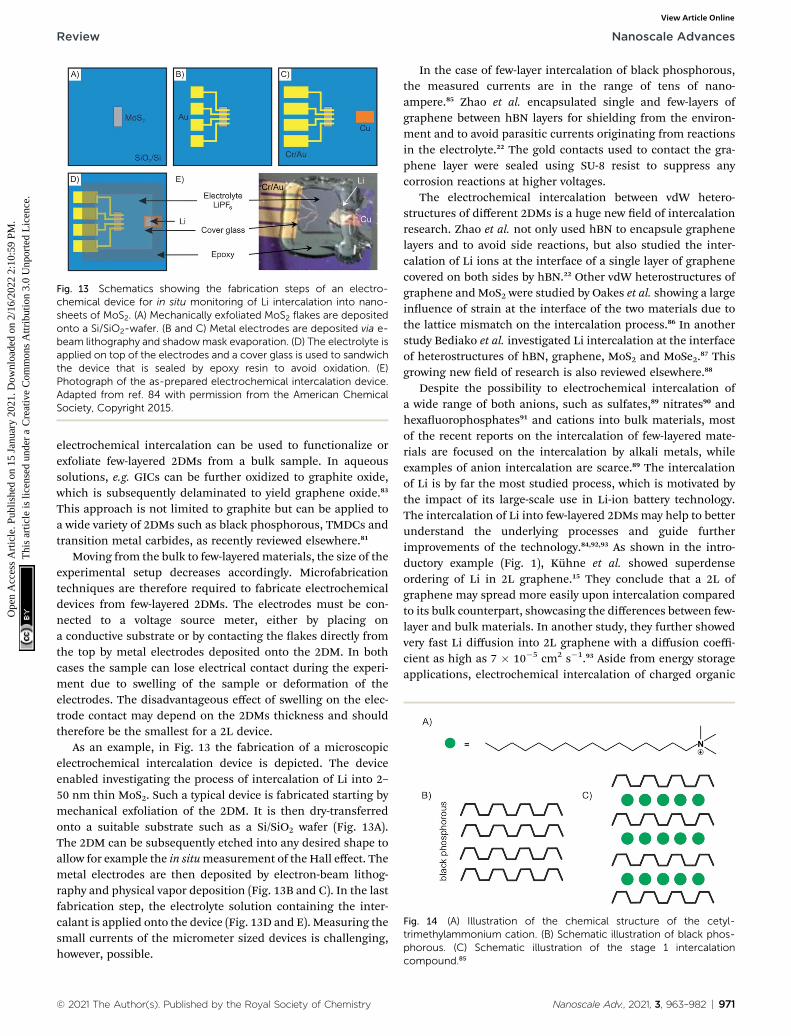
Fig. 13 Schematics showing the fabrication steps of an electro-chemical device for in situ monitoring of Li intercalation into nano-sheets of MoS2. (A) Mechanically exfoliated MoS2 flakes are depositedonto a Si/SiO2-wafer. (B and C) Metal electrodes are deposited via e-beam lithography and shadowmask evaporation. (D) The electrolyte isapplied on top of the electrodes and a cover glass is used to sandwichthe device that is sealed by epoxy resin to avoid oxidation. (E)Photograph of the as-prepared electrochemical intercalation device.Adapted from ref. 84 with permission from the American ChemicalSociety, Copyright 2015.
Fig. 14 (A) Illustration of the chemical structure of the cetyl-trimethylammonium cation. (B) Schematic illustration of black phos-phorous. (C) Schematic illustration of the stage 1 intercalationcompound.85
Review Nanoscale Advances
Ope
n A
cces
s A
rtic
le. P
ublis
hed
on 1
5 Ja
nuar
y 20
21. D
ownl
oade
d on
2/1
6/20
22 2
:10:
59 P
M.
Thi
s ar
ticle
is li
cens
ed u
nder
a C
reat
ive
Com
mon
s A
ttrib
utio
n 3.
0 U
npor
ted
Lic
ence
.View Article Online
electrochemical intercalation can be used to functionalize orexfoliate few-layered 2DMs from a bulk sample. In aqueoussolutions, e.g. GICs can be further oxidized to graphite oxide,which is subsequently delaminated to yield graphene oxide.83
This approach is not limited to graphite but can be applied toa wide variety of 2DMs such as black phosphorous, TMDCs andtransition metal carbides, as recently reviewed elsewhere.81
Moving from the bulk to few-layeredmaterials, the size of theexperimental setup decreases accordingly. Microfabricationtechniques are therefore required to fabricate electrochemicaldevices from few-layered 2DMs. The electrodes must be con-nected to a voltage source meter, either by placing ona conductive substrate or by contacting the akes directly fromthe top by metal electrodes deposited onto the 2DM. In bothcases the sample can lose electrical contact during the experi-ment due to swelling of the sample or deformation of theelectrodes. The disadvantageous effect of swelling on the elec-trode contact may depend on the 2DMs thickness and shouldtherefore be the smallest for a 2L device.
As an example, in Fig. 13 the fabrication of a microscopicelectrochemical intercalation device is depicted. The deviceenabled investigating the process of intercalation of Li into 2–50 nm thin MoS2. Such a typical device is fabricated starting bymechanical exfoliation of the 2DM. It is then dry-transferredonto a suitable substrate such as a Si/SiO2 wafer (Fig. 13A).The 2DM can be subsequently etched into any desired shape toallow for example the in situmeasurement of the Hall effect. Themetal electrodes are then deposited by electron-beam lithog-raphy and physical vapor deposition (Fig. 13B and C). In the lastfabrication step, the electrolyte solution containing the inter-calant is applied onto the device (Fig. 13D and E). Measuring thesmall currents of the micrometer sized devices is challenging,however, possible.
© 2021 The Author(s). Published by the Royal Society of Chemistry
In the case of few-layer intercalation of black phosphorous,the measured currents are in the range of tens of nano-ampere.85 Zhao et al. encapsulated single and few-layers ofgraphene between hBN layers for shielding from the environ-ment and to avoid parasitic currents originating from reactionsin the electrolyte.22 The gold contacts used to contact the gra-phene layer were sealed using SU-8 resist to suppress anycorrosion reactions at higher voltages.
The electrochemical intercalation between vdW hetero-structures of different 2DMs is a huge new eld of intercalationresearch. Zhao et al. not only used hBN to encapsule graphenelayers and to avoid side reactions, but also studied the inter-calation of Li ions at the interface of a single layer of graphenecovered on both sides by hBN.22 Other vdW heterostructures ofgraphene andMoS2 were studied by Oakes et al. showing a largeinuence of strain at the interface of the two materials due tothe lattice mismatch on the intercalation process.86 In anotherstudy Bediako et al. investigated Li intercalation at the interfaceof heterostructures of hBN, graphene, MoS2 and MoSe2.87 Thisgrowing new eld of research is also reviewed elsewhere.88
Despite the possibility to electrochemical intercalation ofa wide range of both anions, such as sulfates,89 nitrates90 andhexauorophosphates91 and cations into bulk materials, mostof the recent reports on the intercalation of few-layered mate-rials are focused on the intercalation by alkali metals, whileexamples of anion intercalation are scarce.89 The intercalationof Li is by far the most studied process, which is motivated bythe impact of its large-scale use in Li-ion battery technology.The intercalation of Li into few-layered 2DMs may help to betterunderstand the underlying processes and guide furtherimprovements of the technology.84,92,93 As shown in the intro-ductory example (Fig. 1), Kuhne et al. showed superdenseordering of Li in 2L graphene.15 They conclude that a 2L ofgraphene may spread more easily upon intercalation comparedto its bulk counterpart, showcasing the differences between few-layer and bulk materials. In another study, they further showedvery fast Li diffusion into 2L graphene with a diffusion coeffi-cient as high as 7 � 10�5 cm2 s�1.93 Aside from energy storageapplications, electrochemical intercalation of charged organic
Nanoscale Adv., 2021, 3, 963–982 | 971

Nanoscale Advances Review
Ope
n A
cces
s A
rtic
le. P
ublis
hed
on 1
5 Ja
nuar
y 20
21. D
ownl
oade
d on
2/1
6/20
22 2
:10:
59 P
M.
Thi
s ar
ticle
is li
cens
ed u
nder
a C
reat
ive
Com
mon
s A
ttrib
utio
n 3.
0 U
npor
ted
Lic
ence
.View Article Online
molecules is used to fabricate well dened organic/vdW-hybridheterostructures.85,94 By applying a potential of�3 V, Wang et al.intercalated multi-layered black phosphorous nanosheets withcetyltrimethylammonium cations (Fig. 14A). The intercalationcould be followed by the response of the electrochemical gatecurrent measured versus the applied voltage. The interlayerdistance increased from 5.24 A to 11.21 A as illustrated inFig. 14B and C. Thereby, superlattices of alternating moleculeand 2DM layers were formed in which the individual phos-phorene layers are electronically decoupled from each other.The decoupling of the phosphorene layers leads to an increasedoptical bandgap, as observed by in situ photoluminescencemeasurements.85
Recently, He et al. performed the electrochemical intercala-tion of the neutral organic semiconductor molecule perylene-3,4,9,10-tetracarboxylic dianhydride (PTCDA) into few-layeredMoS2 demonstrating a powerful design scheme for the fabri-cation of well-dened organic devices.95 This may bridge the gapfrom the research of 2DMs and vdW heterostructures andorganic semiconductor research. Electrochemical intercalationof 2DMs enables a high control over the intercalation process bycontrolling the applied external bias. However, the 2DM mustbe conductive, excluding insulating materials such as hBN.Moreover, electrochemical intercalation requires the fabrica-tion of microscale devices which increases the techniquescomplexity.
3.4 Articial assembly
Articial assembly, as sketched in the introduction, providesthe opportunity to access distinct heterostructures to previouslyintroduced conventional intercalation methods. The structuresto be fabricated are not limited to certain ions or small mole-cules, which tend to intercalate specic hosts. Thus, the arti-cial assembly serves chances to integrate novel building blocksfor the fabrication of few-layered intercalation compounds.However, the increasing freedom of parameters leads tocomplexity and thus a process, which is less controllable. Forexample, the integrity of the lattice of 1Ls may be harmed
Fig. 15 Dry transfer with viscoelastic stamp of PDMS. (A) Tape exfo-liation of bulk 2DM, (B) exfoliated 1L on PDMS, upside down attachedto a glass slide, that PDMS and the target substrate can be aligned bya micromanipulator, (C) contacting PDMS/1L and substrate, (D) lift offof PDMS leaving the 1L on the substrate due to their stronger inter-action, (E) transferred 1L on new substrate.
972 | Nanoscale Adv., 2021, 3, 963–982
during exfoliation and transfer. Thereby cracks or folds may beformed. Furthermore, each process may introduce contami-nants. Moreover, controlling the respective orientations instacked lattices, twisted layers can be formed in which howeverunique properties emerge from lattice mismatch.96–98 Further-more, the orientation of ions/molecules or the number of layersare other degrees of freedom to be considered. However, withovercoming those issues, extraordinary structures withoutstanding properties are created, as outlined in chapter 4.
The mechanical transfer of 2DMs is based on overcomingvdW forces of stacked layers. It is a method to design structuresof twisted layers,97–99 containing molecules,100,101 or of various2DMs, such as graphene, hBN, TMDCs, black phosphorous orsilicene. The yielded structures are also termed as hetero-structures or vdW heterostructures.102–104
The most common transfer method for akes is a dry stamptechnique using polydimethylsiloxane (PDMS) as illustrated inFig. 15. It is an easily handled, clean, fast and reliable techniquecompared to others, like vdW pick up, usage of a sacricial layeror wedging method. Those methods have been extensivelycompared by Frisenda et al.105
With a PDMS stamp a 1L of bulk 2DMs can also be delami-nated, a process, which is similar to the rst invented scotchtape method (Fig. 15A). For the transfer, the ake is picked-upby the PDMS stamp, which is attached to a glass slide. Theglass slide is xed to a micromanipulator. Due to the trans-parency of PDMS, the alignment to an underlying ake orsubstrate can be traced under an optical microscope (Fig. 15B).Aer bringing PDMS and substrate in contact, PDMS can beslowly peeled off leaving the ake behind on the substrate(Fig. 15C–E).
The means of choice for large ake sizes, as can be producedby CVD, is a polymethylmethacrylate (PMMA)-supported etchtransfer method (Fig. 16).106 Therefore, PMMA is dropped ona large 1L, spin casted and dried to stabilize the intact lattice(Fig. 16B). In the case of CVDgrown graphene the underlyingsubstrate is a Cu foil, which is e.g. etched by a Fe(NO3)3 solutionand washed with water. For a Si/SiO2 substrate the removal of
Fig. 16 PMMA supported etching transfer commonly used for largeareas of CVD grownmaterials. (A) 1L on CVD supporting substrate (e.g.copper for CVD graphene). (B) Spin casting of PMMA on top of the 1L.(C) Removal of the substrate by etching. (D) Wet or dry transfer ontonew substrate; wet transfer: after etching, PMMA/1L is washed ina water bath. By decreasing thewater level, the 2DM can be transferredon a new substrate, which is placed at the bottom of the bath; drytransfer: an additional layer of PDMS is fixed on PMMA to handlePMMA/1L without the stabilizing interface of water. (E) PMMA isremoved by acetone leaving the CVD 1L on new substrate.
© 2021 The Author(s). Published by the Royal Society of Chemistry
Review Nanoscale Advances
Ope
n A
cces
s A
rtic
le. P
ublis
hed
on 1
5 Ja
nuar
y 20
21. D
ownl
oade
d on
2/1
6/20
22 2
:10:
59 P
M.
Thi
s ar
ticle
is li
cens
ed u
nder
a C
reat
ive
Com
mon
s A
ttrib
utio
n 3.
0 U
npor
ted
Lic
ence
.View Article Online
the substrate can be achieved by intercalation of water betweenthe hydrophobic polymer/ake and hydrophilic substrate(named wedging transfer method; Fig. 16C). In both casesa subsequent wet-transfer may be performed by decreasing thewater level. However, also a dry transfer is possible (Fig. 16D).107
Finally, PMMA is dissolved in acetone, rinsed and dried, leavingan intact lattice on the desired substrate (Fig. 16E).
Further methods are reported,105,108–111 which are specic formaterials, such as oxo-functionalized graphene,112 TMDCs113 orrequirements due to the shape of the substrate.114
4 Directions of research ofintercalated few-layer 2D materials
With thinning down the z-direction of layered 2DMs, propertieschanges, as introduced in the introduction. In this section, wehighlight some research directions reported for intercalatedfew-layered 2DMs. In particular, we will focus on supercon-ductivity, band-gap tuning, magnetic properties, optical prop-erties, energy storage and chemical reactions.
4.1 Superconductivity
Superconductivity is a general research direction to nd mate-rials, which transport charge carriers at room temperaturewithout resistance. The search for new superconductive mate-rials is ongoing. In 1987 the Nobel prize in Physics was awardedto J. Georg Bednorz and K. Alex Muller “for their importantbreak-through in the discovery of superconductivity in ceramicmaterials”.115 Thereby, the research is based on the preparationof oxo-cuprates. Currently, Hg12Tl3Ba30Ca30Cu45O127 holds theworld record for superconductivity at ambient pressure at 138K.116 Superhydrides, which possess structures of solid atomicmetallic hydrogen, such as LaH10 (ref. 117) show a transitiontemperature of astonishing 259 K, however, at 170 GPa.118 Thecurrent world record holding superconductive materials arebrittle and making km-long wires is not in reach. Thus, super-conductivity in few-layered 2DMs would be the next superlative.Superconductivity is well-known for carbon materials, such asfullerenes,119 carbon nanotubes120 and diamond.121 For gra-phene and doped graphene, superconductivity was predicted,121
and for bulk CaC6, synthesized from graphite and Li–Ca alloy,superconductivity was reported below 11.5 K.122 A surprisingdiscovery in this eld was reported in 2018 for twisted 2L
Fig. 17 Illustration of the structure of superconductive Ca-interca-lated 2L graphene. (A) Top view with graphene lattice in grey andposition of Ca atoms in yellow. (B) Sectional view illustrating thelayered structure.124
© 2021 The Author(s). Published by the Royal Society of Chemistry
graphene with a twisting angle of 1.1�. At this “magic-angle”superconductivity is occurring at 1.7 K.97,123 In 2016 Ca inter-calated 2L graphene (C6CaC6) was reported to be supercon-ductive at 4 K.124 The structure was prepared from epitaxial 2Lgraphene. First Li atoms were intercalated and then exchangedby Ca (Fig. 17). Although this temperature is lower compared tothe bulk, the experiment demonstrates that superconductiveproperties remain in 2L. Also other intercalated 2DMs are pre-dicted to be superconductive, such as 2L borophene (B2MgB2)below 23 K.125
4.2 Band gap tuning
In this section, we highlight the possibilities to tune the elec-tronic properties of 2L and 3L graphene by intercalation. Sincegraphene lacks a band gap, conventional transistors with Ion/Ioffratios >106 are by far not possible.12,126 Thus, opening a bandgap is necessary to generate a transistor behaviour withreasonable Ion/Ioff ratios. Breaking the inversion symmetry in 2Lgraphene is one way to induce a band gap.127 It was reportedthat dual gating of 2L graphene can open a band gap, reachingeven an insulating state.128 With tuning the voltages of the topand bottom gate, tuning of the band gap of 2L graphene wasdemonstrated with values up to 250 eV.129 Instead of dual-gatingalso intercalation/surface chemistry can induce a band gap.
Using density functional theory with vdW density functional,it was predicted that 2L graphene can be intercalated between Kon the bottom and FeCl3 on top to open a band gap in 2L gra-phene with application relevant 0.4 eV coming into reach.132
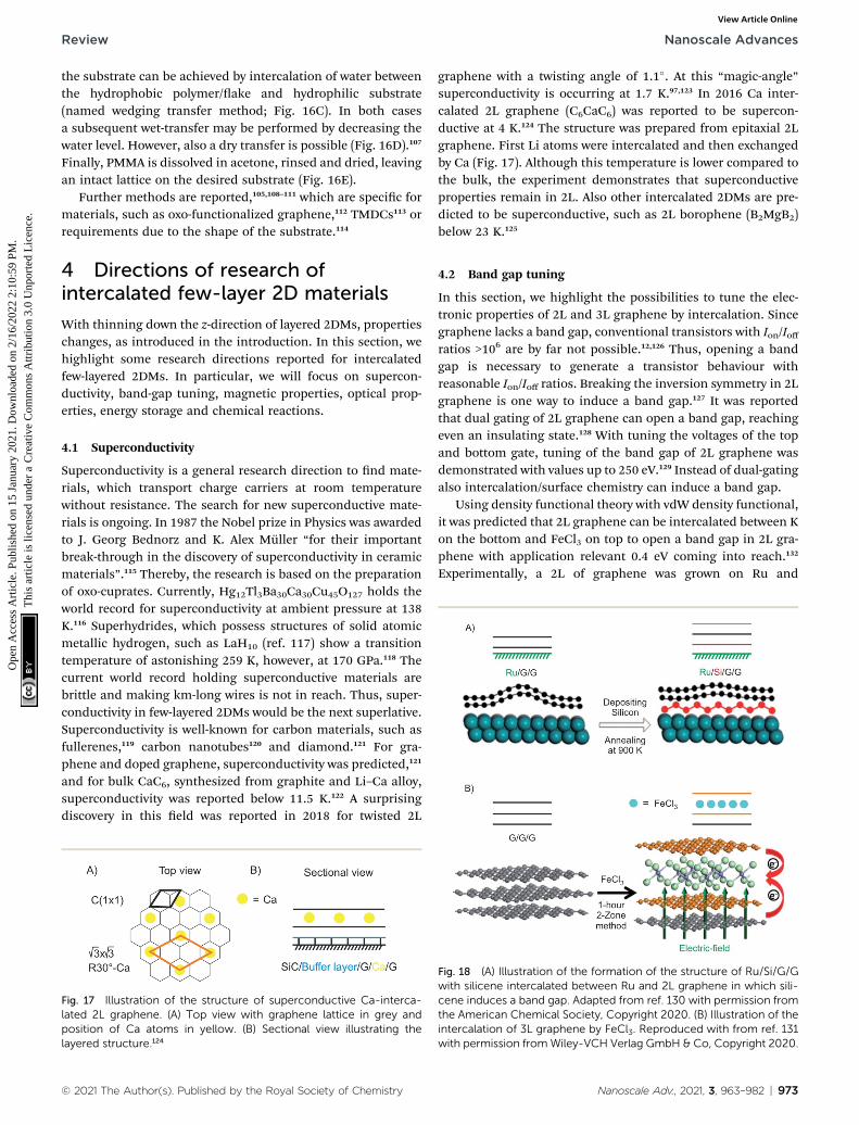
Experimentally, a 2L of graphene was grown on Ru and
Fig. 18 (A) Illustration of the formation of the structure of Ru/Si/G/Gwith silicene intercalated between Ru and 2L graphene in which sili-cene induces a band gap. Adapted from ref. 130 with permission fromthe American Chemical Society, Copyright 2020. (B) Illustration of theintercalation of 3L graphene by FeCl3. Reproduced with from ref. 131with permission fromWiley-VCH Verlag GmbH & Co, Copyright 2020.
Nanoscale Adv., 2021, 3, 963–982 | 973
Nanoscale Advances Review
Ope
n A
cces
s A
rtic
le. P
ublis
hed
on 1
5 Ja
nuar
y 20
21. D
ownl
oade
d on
2/1
6/20
22 2
:10:
59 P
M.
Thi
s ar
ticle
is li
cens
ed u
nder
a C
reat
ive
Com
mon
s A
ttrib
utio
n 3.
0 U
npor
ted
Lic
ence
.View Article Online
subsequently intercalated by silicene (Fig. 18A). It is reportedthat the layer of silicene, which is intercalated between Ru andthe 2L of graphene induces a band gap of about 0.2 eV.130 Inanother approach 3L graphene, prepared by mechanicalcleavage, was intercalated by FeCl3 by the two-zone method(Fig. 18B). Under the experimental conditions a stage 2 inter-calation product is obtained, as evidenced by a splited G peak inthe Raman spectrum. A band gap of 0.13 eV was calculated forthe experimentally obtained structure. In addition, the authorsreport that the intercalation compound is stable in ambientconditions.131 In general, the decomposition of FeCl3 interca-lated graphite is kinetically hindered, since water must diffuseinto the interlayers. It is described that [FeCl2(OH2)4]
+ and 4 Cl�
are initially formed by the reaction of 4 H2O and [FeCl6]3�.
Subsequently, [FeCl4]� ions are formed, which are less densely
packed.133
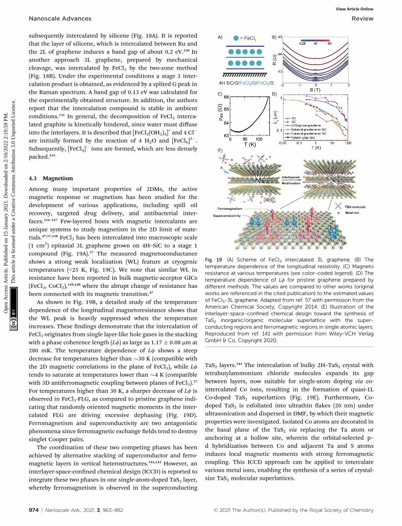
Fig. 19 (A) Scheme of FeCl3 intercalated 3L graphene. (B) Thetemperature dependence of the longitudinal resistivity. (C) Magnetoresistance at various temperatures (see color-coded legend). (D) Thetemperature dependence of Lf for pristine graphene prepared bydifferent methods. The values are compared to other works (originalworks are referenced in the cited publication) to the estimated valuesof FeCl3-3L graphene. Adapted from ref. 57 with permission from theAmerican Chemical Society, Copyright 2014. (E) Illustration of theinterlayer-space-confined chemical design toward the synthesis ofTaS2 inorganic/organic molecular superlattice with the super-conducting regions and ferromagnetic regions in single atomic layers.Reproduced from ref. 141 with permission from Wiley-VCH VerlagGmbH & Co, Copyright 2020.
4.3 Magnetism
Among many important properties of 2DMs, the activemagnetic response or magnetism has been studied for thedevelopment of various applications, including spill oilrecovery, targeted drug delivery, and antibacterial inter-faces.134–137 Few-layered hosts with magnetic intercalants areunique systems to study magnetism in the 2D limit of mate-rials.47,57,138 FeCl3 has been intercalated into macroscopic scale(1 cm2) epitaxial 3L graphene grown on 4H–SiC to a stage 1compound (Fig. 19A).57 The measured magnetoconductanceshows a strong weak localization (WL) feature at cryogenictemperatures (<25 K, Fig. 19C). We note that similar WL inresistance have been reported in bulk magnetic-acceptor GICs(FeCl3, CoCl2),139,140 where the abrupt change of resistance hasbeen connected with its magnetic transition.47
As shown in Fig. 19B, a detailed study of the temperaturedependence of the longitudinal magnetoresistance shows thatthe WL peak is heavily suppressed when the temperatureincreases. These ndings demonstrate that the intercalation ofFeCl3 originates from single layer-like hole gases in the stackingwith a phase coherence length (Lf) as large as 1.17 � 0.08 mm at280 mK. The temperature dependence of Lf shows a steepdecrease for temperatures higher than �30 K (compatible withthe 2D magnetic correlations in the plane of FeCl3), while Lftends to saturate at temperatures lower than �4 K (compatiblewith 3D antiferromagnetic coupling between planes of FeCl3).57
For temperatures higher than 30 K, a sharper decrease of Lf isobserved in FeCl3-FLG, as compared to pristine graphene indi-cating that randomly oriented magnetic moments in the inter-calated FLG are driving excessive dephasing (Fig. 19D).Ferromagnetism and superconductivity are two antagonisticphenomena since ferromagnetic exchange elds tend to destroysinglet Cooper pairs.
The coordination of these two competing phases has beenachieved by alternative stacking of superconductor and ferro-magnetic layers in vertical heterostructures.142,143 However, aninterlayer-space-conned chemical design (ICCD) is reported tointegrate these two phases in one single-atom-doped TaS2 layer,whereby ferromagnetism is observed in the superconducting
974 | Nanoscale Adv., 2021, 3, 963–982
TaS2 layers.141 The intercalation of bulky 2H–TaS2 crystal withtetrabutylammonium chloride molecules expands its gapbetween layers, now suitable for single-atom doping via co-intercalated Co ions, resulting in the formation of quasi-1LCo-doped TaS2 superlattices (Fig. 19E). Furthermore, Co-doped TaS2 is exfoliated into ultrathin akes (20 nm) underultrasonication and dispersed in DMF, by which their magneticproperties were investigated. Isolated Co atoms are decorated inthe basal plane of the TaS2 via replacing the Ta atom oranchoring at a hollow site, wherein the orbital-selected p–d hybridization between Co and adjacent Ta and S atomsinduces local magnetic moments with strong ferromagneticcoupling. This ICCD approach can be applied to intercalatevarious metal ions, enabling the synthesis of a series of crystal-size TaS2 molecular superlattices.
© 2021 The Author(s). Published by the Royal Society of Chemistry
Review Nanoscale Advances
Ope
n A
cces
s A
rtic
le. P
ublis
hed
on 1
5 Ja
nuar
y 20
21. D
ownl
oade
d on
2/1
6/20
22 2
:10:
59 P
M.
Thi
s ar
ticle
is li
cens
ed u
nder
a C
reat
ive
Com
mon
s A
ttrib
utio
n 3.
0 U
npor
ted
Lic
ence
.View Article Online
4.4 Optical properties
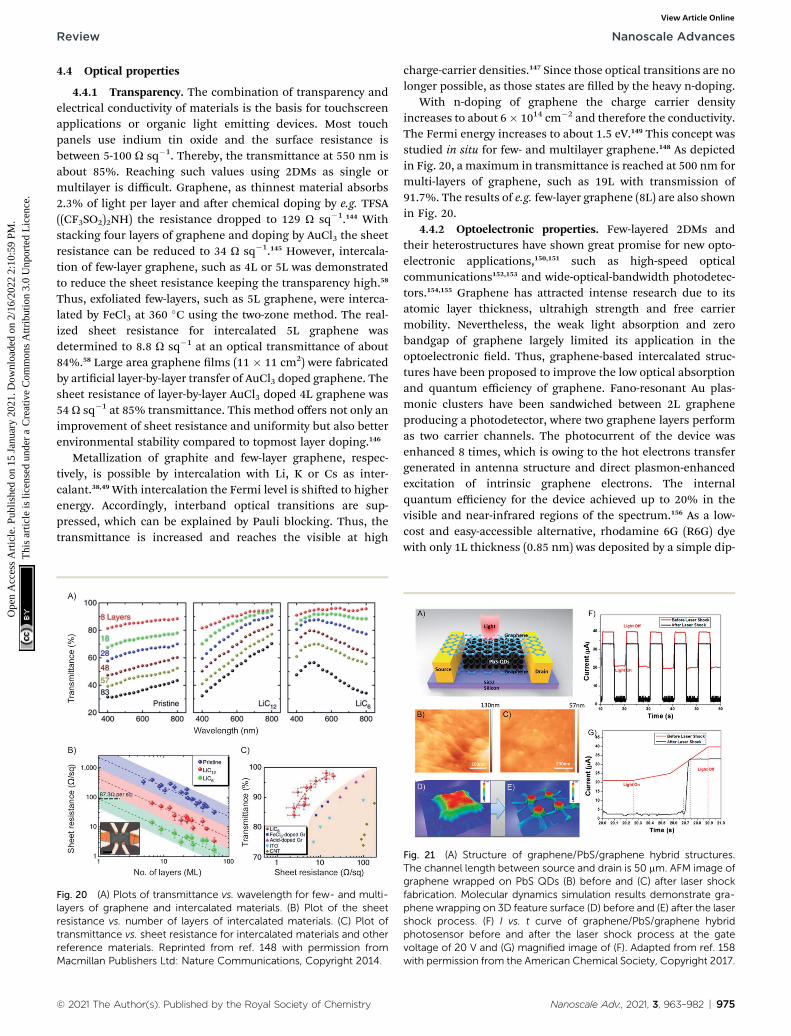
4.4.1 Transparency. The combination of transparency andelectrical conductivity of materials is the basis for touchscreenapplications or organic light emitting devices. Most touchpanels use indium tin oxide and the surface resistance isbetween 5-100 U sq�1. Thereby, the transmittance at 550 nm isabout 85%. Reaching such values using 2DMs as single ormultilayer is difficult. Graphene, as thinnest material absorbs2.3% of light per layer and aer chemical doping by e.g. TFSA((CF3SO2)2NH) the resistance dropped to 129 U sq�1.144 Withstacking four layers of graphene and doping by AuCl3 the sheetresistance can be reduced to 34 U sq�1.145 However, intercala-tion of few-layer graphene, such as 4L or 5L was demonstratedto reduce the sheet resistance keeping the transparency high.58
Thus, exfoliated few-layers, such as 5L graphene, were interca-lated by FeCl3 at 360 �C using the two-zone method. The real-ized sheet resistance for intercalated 5L graphene wasdetermined to 8.8 U sq�1 at an optical transmittance of about84%.58 Large area graphene lms (11 � 11 cm2) were fabricatedby articial layer-by-layer transfer of AuCl3 doped graphene. Thesheet resistance of layer-by-layer AuCl3 doped 4L graphene was54 U sq�1 at 85% transmittance. This method offers not only animprovement of sheet resistance and uniformity but also betterenvironmental stability compared to topmost layer doping.146
Metallization of graphite and few-layer graphene, respec-tively, is possible by intercalation with Li, K or Cs as inter-calant.38,49 With intercalation the Fermi level is shied to higherenergy. Accordingly, interband optical transitions are sup-pressed, which can be explained by Pauli blocking. Thus, thetransmittance is increased and reaches the visible at high
Fig. 20 (A) Plots of transmittance vs. wavelength for few- and multi-layers of graphene and intercalated materials. (B) Plot of the sheetresistance vs. number of layers of intercalated materials. (C) Plot oftransmittance vs. sheet resistance for intercalated materials and otherreference materials. Reprinted from ref. 148 with permission fromMacmillan Publishers Ltd: Nature Communications, Copyright 2014.
© 2021 The Author(s). Published by the Royal Society of Chemistry
charge-carrier densities.147 Since those optical transitions are nolonger possible, as those states are lled by the heavy n-doping.
With n-doping of graphene the charge carrier densityincreases to about 6� 1014 cm�2 and therefore the conductivity.The Fermi energy increases to about 1.5 eV.149 This concept wasstudied in situ for few- and multilayer graphene.148 As depictedin Fig. 20, a maximum in transmittance is reached at 500 nm formulti-layers of graphene, such as 19L with transmission of91.7%. The results of e.g. few-layer graphene (8L) are also shownin Fig. 20.
4.4.2 Optoelectronic properties. Few-layered 2DMs andtheir heterostructures have shown great promise for new opto-electronic applications,150,151 such as high-speed opticalcommunications152,153 and wide-optical-bandwidth photodetec-tors.154,155 Graphene has attracted intense research due to itsatomic layer thickness, ultrahigh strength and free carriermobility. Nevertheless, the weak light absorption and zerobandgap of graphene largely limited its application in theoptoelectronic eld. Thus, graphene-based intercalated struc-tures have been proposed to improve the low optical absorptionand quantum efficiency of graphene. Fano-resonant Au plas-monic clusters have been sandwiched between 2L grapheneproducing a photodetector, where two graphene layers performas two carrier channels. The photocurrent of the device wasenhanced 8 times, which is owing to the hot electrons transfergenerated in antenna structure and direct plasmon-enhancedexcitation of intrinsic graphene electrons. The internalquantum efficiency for the device achieved up to 20% in thevisible and near-infrared regions of the spectrum.156 As a low-cost and easy-accessible alternative, rhodamine 6G (R6G) dyewith only 1L thickness (0.85 nm) was deposited by a simple dip-
Fig. 21 (A) Structure of graphene/PbS/graphene hybrid structures.The channel length between source and drain is 50 mm. AFM image ofgraphene wrapped on PbS QDs (B) before and (C) after laser shockfabrication. Molecular dynamics simulation results demonstrate gra-phene wrapping on 3D feature surface (D) before and (E) after the lasershock process. (F) I vs. t curve of graphene/PbS/graphene hybridphotosensor before and after the laser shock process at the gatevoltage of 20 V and (G) magnified image of (F). Adapted from ref. 158with permission from the American Chemical Society, Copyright 2017.
Nanoscale Adv., 2021, 3, 963–982 | 975
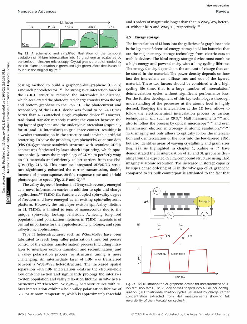
Fig. 22 A schematic and simplified illustration of the temporalevolution of lithium intercalation into 2L graphene as evaluated bytransmission electron microscopy. Crystal grains are color-coded bytheir in-plane orientation in green and light green. More details can befound in the original figure.15
Fig. 23 (A) Illustration the 2L graphene device for measurement of Li-ion diffusion rates. The 2L device was shaped into a Hall bar config-uration. (B) Lithiation/delithiation cycles visualized by charge carrierconcentration extracted from Hall measurements showing full
Nanoscale Advances Review
Ope
n A
cces
s A
rtic
le. P
ublis
hed
on 1
5 Ja
nuar
y 20
21. D
ownl
oade
d on
2/1
6/20
22 2
:10:
59 P
M.
Thi
s ar
ticle
is li
cens
ed u
nder
a C
reat
ive
Com
mon
s A
ttrib
utio
n 3.
0 U
npor
ted
Lic
ence
.View Article Online
coating method to build a graphene–dye–graphene (G–R–G)sandwich photodetector.157 The strong p–p interaction force inthe G–R–G structure reduced the intermolecular distance,which accelerated the photoexcited charge transfer from the topand bottom graphene to the R6G 1L. The photocurrent andresponsivity of the G–R–G device was found to be �40 timesbetter than R6G-attached single-graphene device.157 However,traditional transfer methods restrict the contact between thetop layer of graphene and the underlying intercalant (especiallyfor 0D and 3D intercalant) to grid-space contact, resulting ina weaker transmission in the structure and inevitable articialscattering. To solve the problem, a graphene/PbS-quantum dots(PbS-QDs)/graphene sandwich structure with seamless 2D/0Dcontact was fabricated by laser shock imprinting, which opto-mechanically tunes the morphology of 2DMs to perfectly wrapon 0D materials and efficiently collect carriers from the PbS-QDs (Fig. 21A–E). This seamless integrated 2D/0D/2D struc-ture signicantly enhanced the carrier transmission, doubleincrease of photoresponse, 20-fold response time and 13-foldphotoresponse speed (Fig. 21F and G).158
The valley degree of freedom in 2D-crystals recently emergedas a novel information carrier in addition to spin and chargeapplications.159 TMDC-1Ls feature a coupled spin-valley degreeof freedom and have emerged as an exciting spin/valleytronicplatform. However, the intralayer exciton spin/valley lifetimein 1L TMDCs is limited to tens of nanoseconds due to theunique spin-valley locking behaviour. Achieving long-livedpopulation and polarization lifetimes in TMDC materials is ofcentral importance for their optoelectronic, photonic, and spin/valleytronic applications.
Type II heterostructures, such as WSe2/MoSe2 have beenfabricated to reach long valley polarization times, but precisecontrol of the exciton transformation process (including intra-layer to interlayer exciton transition and recombination) anda valley polarization process via structural tuning is morechallenging. An intermediate layer of hBN was transferredbetween a WSe2/WS2 heterostructure. The increased spatialseparation with hBN intercalation weakens the electron–holeCoulomb interaction and signicantly prolongs the interlayerexciton population and valley relaxation lifetime in vdW heter-ostructures.160 Therefore, WSe2/WS2 heterostructures with 1LhBN intercalation exhibit a hole valley polarization lifetime of�60 ps at room temperature, which is approximately threefold
976 | Nanoscale Adv., 2021, 3, 963–982
and 3 orders of magnitude longer than that inWSe2/WS2 hetero-2L without hBN and WSe2-1L, respectively.160
4.5 Energy storage
The intercalation of Li ions into the galleries of a graphite anodeis the key step of electrical energy storage in Li-ion batteries thatare the major energy storage technology from electric cars tomobile devices. The ideal energy storage device must combinea high energy and power density with a long cycling lifetime.The energy density depends on the amount of charge that canbe stored in the material. The power density depends on howfast the intercalant can diffuse into and out of the layeredmaterial. These two factors should be combined with a highcycling life time, that is a large number of intercalation/deintercalation cycles without signicant performance loss.For the further development of this key technology a thoroughunderstanding of the processes at the atomic level is highlydesired. Studying the intercalation at the 2D level allows tofollow the electrochemical intercalation process by varioustechniques in situ such as XRD,161 Hall measurements22,93 andalso to follow the process by optical microscopy89,162 and eventransmission electron microscopy at atomic resolution.15,93,163
TEM imaging not only allows to optically follow the intercala-tion and deintercalation of the ions into the few-layered 2DM,but also identies areas of varying crystallinity and grain sizes(Fig. 22). As highlighted in chapter 1, Kuhne et al. havedemonstrated the Li intercalation of 2L and 3L graphene devi-ating from the expected C6LiC6 compound structure using TEMimaging at atomic resolution. The increased Li storage capacityby super dense ordering of Li in the vdW gap of 2L graphenecompared to its bulk counterpart is attributed to the fact that
reversibility of the intercalation cycles.93
© 2021 The Author(s). Published by the Royal Society of Chemistry
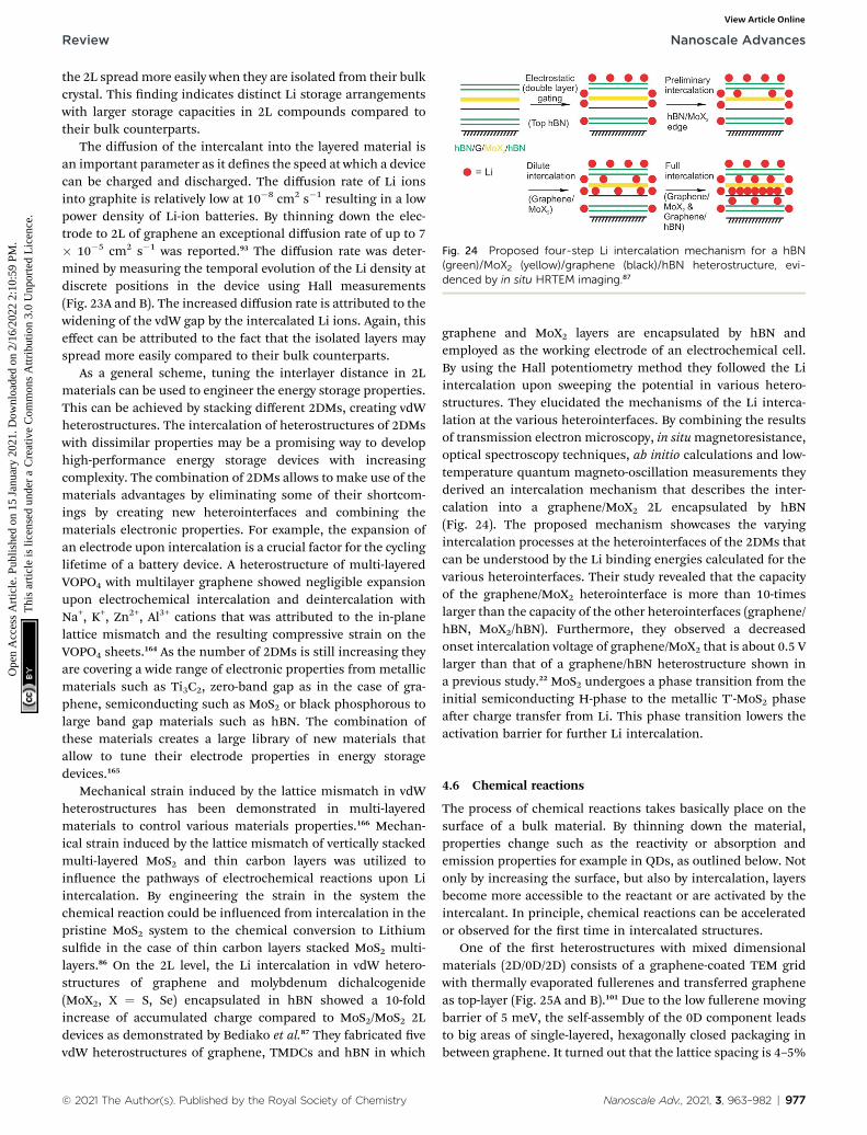
Fig. 24 Proposed four-step Li intercalation mechanism for a hBN(green)/MoX2 (yellow)/graphene (black)/hBN heterostructure, evi-denced by in situ HRTEM imaging.87
Review Nanoscale Advances
Ope
n A
cces
s A
rtic
le. P
ublis
hed
on 1
5 Ja
nuar
y 20
21. D
ownl
oade
d on
2/1
6/20
22 2
:10:
59 P
M.
Thi
s ar
ticle
is li
cens
ed u
nder
a C
reat
ive
Com
mon
s A
ttrib
utio
n 3.
0 U
npor
ted
Lic
ence
.View Article Online
the 2L spreadmore easily when they are isolated from their bulkcrystal. This nding indicates distinct Li storage arrangementswith larger storage capacities in 2L compounds compared totheir bulk counterparts.
The diffusion of the intercalant into the layered material isan important parameter as it denes the speed at which a devicecan be charged and discharged. The diffusion rate of Li ionsinto graphite is relatively low at 10�8 cm2 s�1 resulting in a lowpower density of Li-ion batteries. By thinning down the elec-trode to 2L of graphene an exceptional diffusion rate of up to 7� 10�5 cm2 s�1 was reported.93 The diffusion rate was deter-mined by measuring the temporal evolution of the Li density atdiscrete positions in the device using Hall measurements(Fig. 23A and B). The increased diffusion rate is attributed to thewidening of the vdW gap by the intercalated Li ions. Again, thiseffect can be attributed to the fact that the isolated layers mayspread more easily compared to their bulk counterparts.
As a general scheme, tuning the interlayer distance in 2Lmaterials can be used to engineer the energy storage properties.This can be achieved by stacking different 2DMs, creating vdWheterostructures. The intercalation of heterostructures of 2DMswith dissimilar properties may be a promising way to develophigh-performance energy storage devices with increasingcomplexity. The combination of 2DMs allows to make use of thematerials advantages by eliminating some of their shortcom-ings by creating new heterointerfaces and combining thematerials electronic properties. For example, the expansion ofan electrode upon intercalation is a crucial factor for the cyclinglifetime of a battery device. A heterostructure of multi-layeredVOPO4 with multilayer graphene showed negligible expansionupon electrochemical intercalation and deintercalation withNa+, K+, Zn2+, Al3+ cations that was attributed to the in-planelattice mismatch and the resulting compressive strain on theVOPO4 sheets.164 As the number of 2DMs is still increasing theyare covering a wide range of electronic properties from metallicmaterials such as Ti3C2, zero-band gap as in the case of gra-phene, semiconducting such as MoS2 or black phosphorous tolarge band gap materials such as hBN. The combination ofthese materials creates a large library of new materials thatallow to tune their electrode properties in energy storagedevices.165
Mechanical strain induced by the lattice mismatch in vdWheterostructures has been demonstrated in multi-layeredmaterials to control various materials properties.166 Mechan-ical strain induced by the lattice mismatch of vertically stackedmulti-layered MoS2 and thin carbon layers was utilized toinuence the pathways of electrochemical reactions upon Liintercalation. By engineering the strain in the system thechemical reaction could be inuenced from intercalation in thepristine MoS2 system to the chemical conversion to Lithiumsulde in the case of thin carbon layers stacked MoS2 multi-layers.86 On the 2L level, the Li intercalation in vdW hetero-structures of graphene and molybdenum dichalcogenide(MoX2, X ¼ S, Se) encapsulated in hBN showed a 10-foldincrease of accumulated charge compared to MoS2/MoS2 2Ldevices as demonstrated by Bediako et al.87 They fabricated vevdW heterostructures of graphene, TMDCs and hBN in which
© 2021 The Author(s). Published by the Royal Society of Chemistry
graphene and MoX2 layers are encapsulated by hBN andemployed as the working electrode of an electrochemical cell.By using the Hall potentiometry method they followed the Liintercalation upon sweeping the potential in various hetero-structures. They elucidated the mechanisms of the Li interca-lation at the various heterointerfaces. By combining the resultsof transmission electron microscopy, in situmagnetoresistance,optical spectroscopy techniques, ab initio calculations and low-temperature quantum magneto-oscillation measurements theyderived an intercalation mechanism that describes the inter-calation into a graphene/MoX2 2L encapsulated by hBN(Fig. 24). The proposed mechanism showcases the varyingintercalation processes at the heterointerfaces of the 2DMs thatcan be understood by the Li binding energies calculated for thevarious heterointerfaces. Their study revealed that the capacityof the graphene/MoX2 heterointerface is more than 10-timeslarger than the capacity of the other heterointerfaces (graphene/hBN, MoX2/hBN). Furthermore, they observed a decreasedonset intercalation voltage of graphene/MoX2 that is about 0.5 Vlarger than that of a graphene/hBN heterostructure shown ina previous study.22 MoS2 undergoes a phase transition from theinitial semiconducting H-phase to the metallic T'-MoS2 phaseaer charge transfer from Li. This phase transition lowers theactivation barrier for further Li intercalation.
4.6 Chemical reactions
The process of chemical reactions takes basically place on thesurface of a bulk material. By thinning down the material,properties change such as the reactivity or absorption andemission properties for example in QDs, as outlined below. Notonly by increasing the surface, but also by intercalation, layersbecome more accessible to the reactant or are activated by theintercalant. In principle, chemical reactions can be acceleratedor observed for the rst time in intercalated structures.
One of the rst heterostructures with mixed dimensionalmaterials (2D/0D/2D) consists of a graphene-coated TEM gridwith thermally evaporated fullerenes and transferred grapheneas top-layer (Fig. 25A and B).101 Due to the low fullerene movingbarrier of 5 meV, the self-assembly of the 0D component leadsto big areas of single-layered, hexagonally closed packaging inbetween graphene. It turned out that the lattice spacing is 4–5%
Nanoscale Adv., 2021, 3, 963–982 | 977
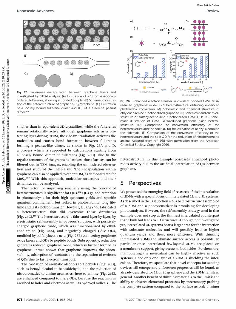
Fig. 25 Fullerenes encapsulated between graphene layers andinvestigated by STEM analysis. (A) Illustration of a 1L of hexagonallyordered fullerenes, showing a bonded couple. (B) Schematic illustra-tion of the heterostructure of graphene/C60/graphene. (C) Illustrationof a loosely bound fullerene dimer and (D) of a fullerene peanutdimer.101
Fig. 26 Enhanced electron transfer in covalent bonded CdSe QDs/reduced graphene oxide (GR) heterostructure obtaining enhancedphotoredox conversion. (A) Schematic and chemical structure ofethylenediamine functionalized graphene. (B) Schematic and chemicalstructure of sulfanylacetic acid functionalized CdSe QDs. (C) Sche-matic illustration of CdSe QDs/reduced graphene oxide hetero-structure. (D) Comparison of conversion efficiency of theheterostructure and the sole QD for the oxidation of benzyl alcohol tothe aldehyde. (E) Comparison of the conversion efficiency of theheterostructure and the sole QD for the reduction of nitrobenzene toaniline. Adapted from ref. 168 with permission from the AmericanChemical Society, Copyright 2019.
Nanoscale Advances Review
Ope
n A
cces
s A
rtic
le. P
ublis
hed
on 1
5 Ja
nuar
y 20
21. D
ownl
oade
d on
2/1
6/20
22 2
:10:
59 P
M.
Thi
s ar
ticle
is li
cens
ed u
nder
a C
reat
ive
Com
mon
s A
ttrib
utio
n 3.
0 U
npor
ted
Lic
ence
.View Article Online
smaller than in equivalent 3D crystallites, while the fullerenesremain rotationally active. Although graphene acts as a pro-tecting layer during STEM, the e-beam irradiation activates themolecules and causes bond formation between fullerenesforming a peanut-like dimer, as shown in Fig. 25A and D,a process which is supported by calculations starting froma loosely bound dimer of fullerenes (Fig. 25C). Due to theregular structure of the graphene lattices, those lattices can beltered out in TEM images, enabling the unhindered observa-tion and study of the intercalant. The encapsulation withingraphene can also be applied to other 2DM, as demonstrated forMoS2.167 With this approach, molecular structures and theirdynamics can be analyzed.
The factor for improving reactivity using the concept ofheterostructures is signicant for QDs.168 QDs gained attentionin photocatalysis for their high quantum yields and specicquantum connement, but lacked in photostability, long life-time and fast electron transfer. However, Huang et al. fabricateda heterostructure that did overcome those drawbacks(Fig. 26C).168 The heterostructure is fabricated layer-by-layer, byelectrostatic self-assembly in aqueous solution, with positivelycharged graphene oxide, which was functionalized by ethyl-enediamine (Fig. 26A), and negatively charged CdSe QDs,modied by sulfanylacetic acid (Fig. 26B) connecting grapheneoxide layers and QDs by peptide bonds. Subsequently, reductiongenerates reduced graphene oxide, which is further termed asgraphene. It was shown that graphene improves the photo-stability, adsorption of reactants and the separation of excitonsof QDs due to fast electron transport.
The oxidation of aromatic alcohols to aldehydes (Fig. 26D),such as benzyl alcohol to benzaldehyde, and the reduction ofnitroaromatics to amino aromatics, here to aniline (Fig. 26E),are enhanced compared to mere QDs, because the reactivity isascribed to holes and electrons as well as hydroxyl radicals. The
978 | Nanoscale Adv., 2021, 3, 963–982
heterostructure in this example possesses enhanced photo-redox activity due to the articial intercalation of QD betweengraphene.
5 Perspectives
We presented the emerging eld of research of the intercalationof 2DMs with a special focus on intercalated 2L and 3L systems.As described in the last Section 4.6, a heterostructure assembledof a 2DM and a photosensitizer is promising for developingphotocatalysts. However, the self-assembly strategy used in thatexample does not stop at the thinnest intercalated counterpartto the bulk but leads to 3D structures. Although not investigatedyet, intercalated 2L systems bear a larger area for the interactionwith substrate molecules and will possibly lead to higherquantum yields and thus, more efficiency. With thinningintercalated 2DMs the ultimate surface access is possible, inparticular once intercalated few-layered 2DMs are placed ona membrane support, giving access to both sides. Furthermore,manipulating the intercalant can be highly effective in suchsystems, since only one layer of a 2DM is shielding the inter-calant. Therefore, we speculate that novel concepts for sensingdevices will emerge and unforeseen properties will be found, asalready described for 1L or 2L graphene and the 2DMs family ingeneral. Another benet of thinning materials to the limit is theability to observe elemental processes by spectroscopy probingthe complete system compared to the surface as only a minor
© 2021 The Author(s). Published by the Royal Society of Chemistry
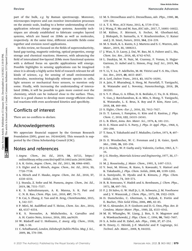
Review Nanoscale Advances
Ope
n A
cces
s A
rtic
le. P
ublis
hed
on 1
5 Ja
nuar
y 20
21. D
ownl
oade
d on
2/1
6/20
22 2
:10:
59 P
M.
Thi
s ar
ticle
is li
cens
ed u
nder
a C
reat
ive
Com
mon
s A
ttrib
utio
n 3.
0 U
npor
ted
Lic
ence
.View Article Online
part of the bulk, e.g. by Raman spectroscopy. Moreover,microscopes improve and can monitor intercalation processeson the atomic scale, leading to a better understanding of evenapplication relevant charge storage systems. Assembly tech-niques are already established to fabricate complex layeredsystems, which are based on 2DMs as well as molecules,respectively. At the same time, different scientic elds cometogether and envision novel applications.
In this review, we focused on the elds of superconductivity,band gap tuning, magnetic ordering, optical properties, energystorage and chemical reactions. However, with advancing theeld of intercalated few-layered 2DMs more functional systemswith a dened focus on specic applications will emerge.Possible highlights in sensing applications can be imaginedsince it is already a highly active eld of research relevant for allkinds of science, e.g. for sensing of small environmentalmolecules, monitoring biologically relevant species in cells,light sensors or mechanical force sensors, to mention onlysome. Finally, with increasing the understanding of interca-lated 2DMs, it will be possible to gain more control over thechemistry, which can be induced close to the surface. Thus,there is a good chance to develop more energy-efficient chem-ical reactions with even accelerated kinetics and specicity.
Conflicts of interest
There are no conicts to declare.
Acknowledgements
We appreciate nancial support by the German ResearchFoundation (DFG, grant no. 392444269). This research is sup-ported by the China Scholarship Council (CSC).
Notes and references
1 Angew. Chem., Int. Ed., 2019, 58, 16723, https://onlinelibrary.wiley.com/doi/epdf/10.1002/anie.201912886.
2 A. K. Geim, Angew. Chem., Int. Ed., 2011, 50, 6966–6985.3 S. Eigler and A. Hirsch, Angew. Chem., Int. Ed., 2014, 53,7720–7738.
4 A. Hirsch and F. Hauke, Angew. Chem., Int. Ed., 2018, 57,4338–4354.
5 J. Sturala, Z. Sofer and M. Pumera, Angew. Chem., Int. Ed.,2019, 58, 7551–7557.
6 K. S. Subrahmanyam, A. K. Manna, S. K. Pati andC. N. R. Rao, Chem. Phys. Lett., 2010, 497, 70–75.
7 B. Cai, S. Zhang, Z. Yan and H. Zeng, ChemNanoMat, 2015,1, 542–557.
8 P. Miro, M. Audiffred and T. Heine, Chem. Soc. Rev., 2014,43, 6537–6554.
9 K. S. Novoselov, A. Mishchenko, A. Carvalho andA. H. Castro Neto, Science, 2016, 353, aac9439.
10 W. Rudorff and U. Hofmann, Z. Anorg. Allg. Chem., 1938,238, 1–50.
11 C. Schaaeutl, London, Edinburgh Dublin Philos. Mag. J. Sci.,2009, 16, 570–590.
© 2021 The Author(s). Published by the Royal Society of Chemistry
12 M. S. Dresselhaus and G. Dresselhaus, Adv. Phys., 1980, 30,139–326.
13 A. T. S. Wee, ACS Nano, 2012, 6, 5739–5741.14 J. Wang, F. Ma and M. Sun, RSC Adv., 2017, 7, 16801–16822.15 M. Kuhne, F. Borrnert, S. Fecher, M. Ghorbani-Asl,
J. Biskupek, D. Samuelis, A. V. Krasheninnikov, U. Kaiserand J. H. Smet, Nature, 2018, 564, 234–239.
16 M. S. Stark, K. L. Kuntz, S. J. Martens and S. C. Warren, Adv.Mater., 2019, 31, 1808213.
17 J. Wan, S. D. Lacey, J. Dai, W. Bao, M. S. Fuhrer and L. Hu,Chem. Soc. Rev., 2016, 45, 6742–6765.
18 L. Daukiya, M. N. Nair, M. Cranney, F. Vonau, S. Hajjar-Garreau, D. Aubel and L. Simon, Prog. Surf. Sci., 2019, 94,1–20.
19 Y. Li, Y. Lu, P. Adelhelm, M.-M. Titirici and Y.-S. Hu, Chem.Soc. Rev., 2019, 48, 4655–4687.
20 A. Lerf, Dalton Trans., 2014, 43, 10276–10291.21 A. Jain, P. Bharadwaj, S. Heeg, M. Parzefall, T. Taniguchi,
K. Watanabe and L. Novotny, Nanotechnology, 2018, 29,265203.
22 S. Y. F. Zhao, G. A. Elbaz, D. K. Bediako, C. Yu, D. K. Efetov,Y. Guo, J. Ravichandran, K.-A. Min, S. Hong, T. Taniguchi,K. Watanabe, L. E. Brus, X. Roy and P. Kim, Nano Lett.,2018, 18, 460–466.
23 S. Eigler, Chem.–Eur. J., 2016, 22, 7012–7027.24 D. T. Larson, I. Fampiou, G. Kim and E. Kaxiras, J. Phys.
Chem. C, 2018, 122, 24535–24541.25 L. B. Ebert, Annu. Rev. Mater. Sci., 1976, 6, 181–211.26 D. E. Nixon and G. S. Parry, J. Phys. D: Appl. Phys., 1968, 1,
291–298.27 T. Sasa, Y. Takahashi and T. Mukaibo, Carbon, 1971, 9, 407–
416.28 D. E. Wessbecher, W. C. Forsman and J. R. Gaier, Synth.
Met., 1988, 26, 185–194.29 J. G. Hooley, W. P. Garby and J. Valentin, Carbon, 1965, 3, 7–
16.30 J. G. Hooley,Materials Science and Engineering, 1977, 31, 17–
24.31 M. J. Rosseinsky, J. Mater. Chem., 1995, 5, 1497–1513.32 Y. Iwai, M. Hirose, R. Kano, S. Kawasaki, Y. Hattori and
K. Takahashi, J. Phys. Chem. Solids, 2008, 69, 1199–1202.33 A. Sumiyoshi, H. Hyodo and K. Kimura, J. Phys. Chem.
Solids, 2010, 71, 569–571.34 R. B. Somoano, V. Hadek and A. Rembaum, J. Chem. Phys.,
1973, 58, 697–701.35 F. J. Di Salvo, G. W. Hull Jr, L. H. Schwartz, J. M. Voorhoeve
and J. V. Waszczak, J. Chem. Phys., 1973, 59, 1922–1929.36 D. Dumchenko, C. Gherman, L. Kulyuk, E. Fortin and
E. Bucher, Thin Solid Films, 2006, 495, 82–85.37 M. G. Alexander, D. P. Goshorn and D. G. Onn, Phys. Rev. B:
Condens. Matter Mater. Phys., 1980, 22, 4535–4542.38 M. H. Whangbo, W. Liang, J. Ren, S. N. Magonov and
A. Wawkuschewski, J. Phys. Chem. C, 1994, 98, 7602–7607.39 S. A. Solin and H. Zabel, Adv. Phys., 1988, 37, 87–254.40 N. Emery, C. Herold, J.-F. Mareche and P. Lagrange, Sci.
Technol. Adv. Mater., 2008, 9, 044102.
Nanoscale Adv., 2021, 3, 963–982 | 979
Nanoscale Advances Review
Ope
n A
cces
s A
rtic
le. P
ublis
hed
on 1
5 Ja
nuar
y 20
21. D
ownl
oade
d on
2/1
6/20
22 2
:10:
59 P
M.
Thi
s ar
ticle
is li
cens
ed u
nder
a C
reat
ive
Com
mon
s A
ttrib
utio
n 3.
0 U
npor
ted
Lic
ence
.View Article Online
41 W. Krone, G. Wortmann and G. Kaindl, Synth. Met., 1989,29, 247–252.
42 J. G. Hooley and M. Bartlett, Carbon, 1967, 5, 417–422.43 J. G. Hooley, Carbon, 1973, 11, 225–236.44 L. Salamanca-Riba, G. Roth, J. M. Gibson, A. R. Kortan,
G. Dresselhaus and R. J. Birgeneau, Phys. Rev. B: Condens.Matter Mater. Phys., 1986, 33, 2738–2748.
45 C. Zeller, L. A. Pendrys and F. L. Vogel, J. Mater. Sci., 1979,14, 2241–2248.
46 A. R. Beal and W. Y. Liang, Philos. Mag., 2006, 27, 1397–1416.
47 N. Kim, K. S. Kim, N. Jung, L. Brus and P. Kim, Nano Lett.,2011, 11, 860–865.
48 M. E. Huster, P. A. Heiney, V. B. Cajipe and J. E. Fischer,Phys. Rev. B: Condens. Matter Mater. Phys., 1987, 35, 3311–3326.
49 N. Jung, B. Kim, A. C. Crowther, N. Kim, C. Nuckolls andL. Brus, ACS Nano, 2011, 5, 5708–5716.
50 N. Jung, N. Kim, S. Jockusch, N. J. Turro, P. Kim and L. Brus,Nano Lett., 2009, 9, 4133–4137.
51 N. Jung, A. C. Crowther, N. Kim, P. Kim and L. Brus, ACSNano, 2010, 4, 7005–7013.
52 J. G. Hooley, Carbon, 1972, 10, 155–163.53 C.-J. Shih, A. Vijayaraghavan, R. Krishnan, R. Sharma,
J.-H. Han, M.-H. Ham, Z. Jin, S. Lin, G. L. C. Paulus,N. F. Reuel, Q. H. Wang, D. Blankschtein andM. S. Strano, Nat. Nanotechnol., 2011, 6, 439–445.
54 D. J. Wehenkel, T. H. Bointon, T. Booth, P. Bøggild,M. F. Craciun and S. Russo, Sci. Rep., 2015, 5, 7609.
55 D. Zhan, L. Sun, Z. H. Ni, L. Liu, X. F. Fan, Y. Wang, T. Yu,Y. M. Lam, W. Huang and Z. X. Shen, Adv. Funct. Mater.,2010, 20, 3504–3509.
56 W. Zhao, P. H. Tan, J. Liu and A. C. Ferrari, J. Am. Chem.Soc., 2011, 133, 5941–5946.
57 T. H. Bointon, I. Khrapach, R. Yakimova, A. V. Shytov,M. F. Craciun and S. Russo, Nano Lett., 2014, 14, 1751–1755.
58 I. Khrapach, F. Withers, T. H. Bointon, D. K. Polyushkin,W. L. Barnes, S. Russo and M. F. Craciun, Adv. Mater.,2012, 24, 2844–2849.
59 W. S. Hummers Jr and R. E. Offeman, J. Am. Chem. Soc.,1958, 80, 1339.
60 S. Eigler, Commun. Chem., 2015, 51, 3162–3165.61 S. Seiler, C. E. Halbig, F. Grote, P. Rietsch, F. Borrnert,
U. Kaiser, B. Meyer and S. Eigler, Nat. Commun., 2018, 9,836.
62 W. J. Zhao, P. H. Tan, J. Zhang and J. Liu, Phys. Rev. B:Condens. Matter Mater. Phys., 2010, 82, 245423.
63 A. Das, B. Chakraborty, S. Piscanec, S. Pisana, A. K. Soodand A. C. Ferrari, Phys. Rev. B: Condens. Matter Mater.Phys., 2009, 79, 155417.
64 K. J. Koski, C. D. Wessells, B. W. Reed, J. J. Cha, D. Kong andY. Cui, J. Am. Chem. Soc., 2012, 134, 13773–13779.
65 K. J. Koski, J. J. Cha, B. W. Reed, C. D. Wessells, D. Kong andY. Cui, J. Am. Chem. Soc., 2012, 134, 7584–7587.
66 K. P. Chen, F. R. Chung, M. Wang and K. J. Koski, J. Am.Chem. Soc., 2015, 137, 5431–5437.
980 | Nanoscale Adv., 2021, 3, 963–982
67 Y. Gong, H. Yuan, C.-L. Wu, P. Tang, S.-Z. Yang, A. Yang,G. Li, B. Liu, J. van de Groep, M. L. Brongersma,M. F. Chisholm, S.-C. Zhang, W. Zhou and Y. Cui, Nat.Nanotechnol., 2018, 13, 294–299.
68 M. Wang, I. Al-Dhahir, J. Appiah and K. J. Koski, Chem.Mater., 2017, 29, 1650–1655.
69 J. P. Motter, K. J. Koski and Y. Cui, Chem. Mater., 2014, 26,2313–2317.
70 M. Wang and K. J. Koski, ACS Nano, 2015, 9, 3226–3233.71 N. C. Osti, M. Naguib, A. Ostadhossein, Y. Xie, P. R. Kent,
B. Dyatkin, G. Rother, W. T. Heller, A. C. van Duin,Y. Gogotsi and E. Mamontov, ACS Appl. Mater. Interfaces,2016, 8, 8859–8863.
72 O. Mashtalir, M. Naguib, V. N. Mochalin, Y. Dall'Agnese,M. Heon, M. W. Barsoum and Y. Gogotsi, Nat. Commun.,2013, 4, 1716.
73 O. Mashtalir, M. R. Lukatskaya, M.-Q. Zhao, M. W. Barsoumand Y. Gogotsi, Adv. Mater., 2015, 27, 3501–3506.
74 M. Naguib, M. Kurtoglu, V. Presser, J. Lu, J. Niu, M. Heon,L. Hultman, Y. Gogotsi and M. W. Barsoum, Adv. Mater.,2011, 23, 4248–4253.
75 J. Li, X. Yuan, C. Lin, Y. Yang, L. Xu, X. Du, J. Xie, J. Lin andJ. Sun, Adv. Energy Mater., 2017, 7, 1602725.
76 J. L. Hart, K. Hantanasirisakul, A. C. Lang, B. Anasori,D. Pinto, Y. Pivak, J. T. van Omme, S. J. May, Y. Gogotsiand M. L. Taheri, Nat. Commun., 2019, 10, 522.
77 M. Boota, M. Pasini, F. Galeotti, W. Porzio, M.-Q. Zhao,J. Halim and Y. Gogotsi, Chem. Mater., 2017, 29, 2731–2738.
78 M. Okubo, A. Sugahara, S. Kajiyama and A. Yamada, Acc.Chem. Res., 2018, 51, 591–599.
79 L. Zhao, R. Zhang, C. Deng, Y. Peng and T. Jiang,Nanomaterials, 2019, 9, 1096.
80 N. I. Kovtyukhova, Y. Wang, R. Lv, M. Terrones, V. H. Crespiand T. E. Mallouk, J. Am. Chem. Soc., 2013, 135, 8372–8381.
81 S. Yang, P. Zhang, A. S. Nia and X. Feng, Adv. Mater., 2020,32, 1907857.
82 J. Zhang, A. Yang, X. Wu, J. van de Groep, P. Tang, S. Li,B. Liu, F. Shi, J. Wan, Q. Li, Y. Sun, Z. Lu, X. Zheng,G. Zhou, C.-L. Wu, S.-C. Zhang, M. L. Brongersma, J. Liand Y. Cui, Nat. Commun., 2018, 9, 5289.
83 J. Cao, P. He, M. A. Mohammed, X. Zhao, R. J. Young,B. Derby, I. A. Kinloch and R. A. W. Dryfe, J. Am. Chem.Soc., 2017, 139, 17446–17456.
84 F. Xiong, H. Wang, X. Liu, J. Sun, M. Brongersma, E. Popand Y. Cui, Nano Lett., 2015, 15, 6777–6784.
85 C. Wang, Q. He, U. Halim, Y. Liu, E. Zhu, Z. Lin, H. Xiao,X. Duan, Z. Feng, R. Cheng, N. O. Weiss, G. Ye,Y.-C. Huang, H. Wu, H.-C. Cheng, I. Shakir, L. Liao,X. Chen, W. A. Goddard III, Y. Huang and X. Duan,Nature, 2018, 555, 231–236.
86 L. Oakes, R. Carter, T. Hanken, A. P. Cohn, K. Share,B. Schmidt and C. L. Pint, Nat. Commun., 2016, 7, 11796.
87 D. K. Bediako, M. Rezaee, H. Yoo, D. T. Larson, S. Y. F. Zhao,T. Taniguchi, K. Watanabe, T. L. Brower-Thomas, E. Kaxirasand P. Kim, Nature, 2018, 558, 425–429.
88 Y. Li, H. Yan, B. Xu, L. Zhen and C.-Y. Xu, Adv. Mater., 2020,2000581.
© 2021 The Author(s). Published by the Royal Society of Chemistry
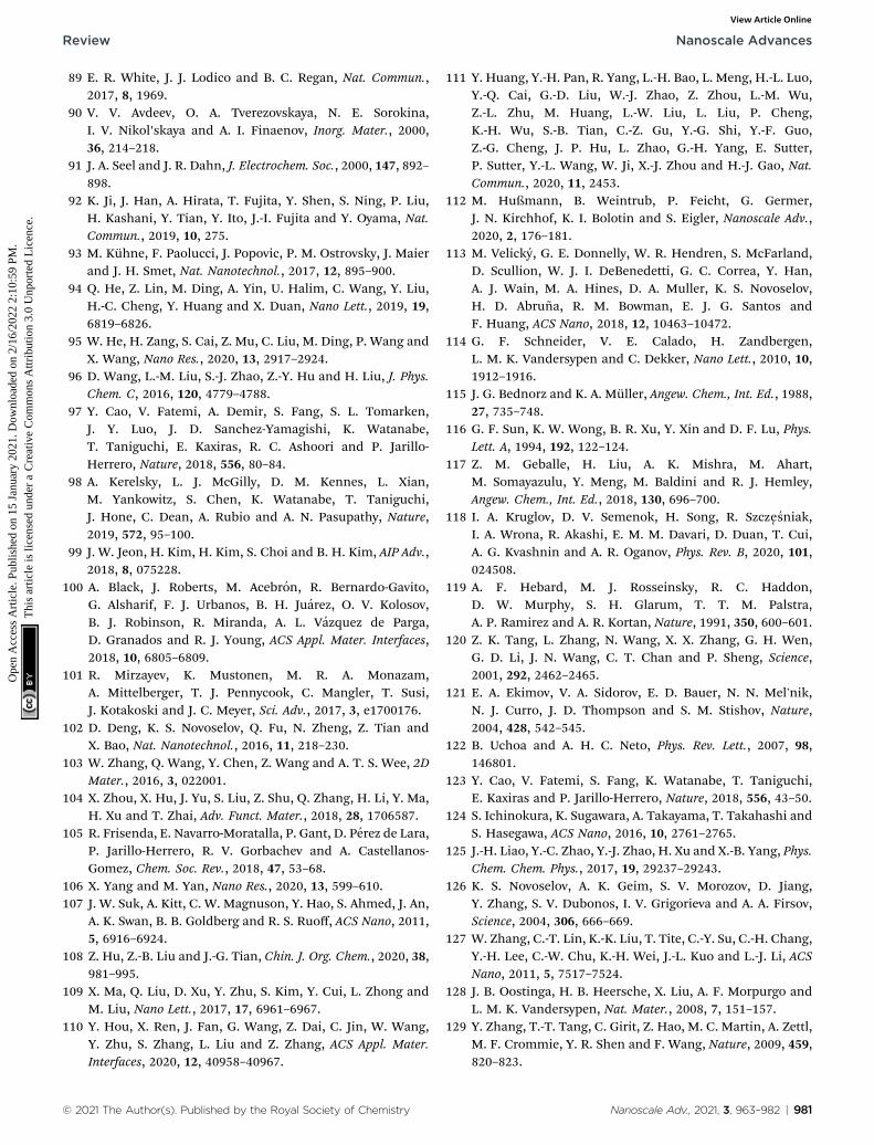
Review Nanoscale Advances
Ope
n A
cces
s A
rtic
le. P
ublis
hed
on 1
5 Ja
nuar
y 20
21. D
ownl
oade
d on
2/1
6/20
22 2
:10:
59 P
M.
Thi
s ar
ticle
is li
cens
ed u
nder
a C
reat
ive
Com
mon
s A
ttrib
utio
n 3.
0 U
npor
ted
Lic
ence
.View Article Online
89 E. R. White, J. J. Lodico and B. C. Regan, Nat. Commun.,2017, 8, 1969.
90 V. V. Avdeev, O. A. Tverezovskaya, N. E. Sorokina,I. V. Nikol’skaya and A. I. Finaenov, Inorg. Mater., 2000,36, 214–218.
91 J. A. Seel and J. R. Dahn, J. Electrochem. Soc., 2000, 147, 892–898.
92 K. Ji, J. Han, A. Hirata, T. Fujita, Y. Shen, S. Ning, P. Liu,H. Kashani, Y. Tian, Y. Ito, J.-I. Fujita and Y. Oyama, Nat.Commun., 2019, 10, 275.
93 M. Kuhne, F. Paolucci, J. Popovic, P. M. Ostrovsky, J. Maierand J. H. Smet, Nat. Nanotechnol., 2017, 12, 895–900.
94 Q. He, Z. Lin, M. Ding, A. Yin, U. Halim, C. Wang, Y. Liu,H.-C. Cheng, Y. Huang and X. Duan, Nano Lett., 2019, 19,6819–6826.
95 W. He, H. Zang, S. Cai, Z. Mu, C. Liu, M. Ding, P. Wang andX. Wang, Nano Res., 2020, 13, 2917–2924.
96 D. Wang, L.-M. Liu, S.-J. Zhao, Z.-Y. Hu and H. Liu, J. Phys.Chem. C, 2016, 120, 4779–4788.
97 Y. Cao, V. Fatemi, A. Demir, S. Fang, S. L. Tomarken,J. Y. Luo, J. D. Sanchez-Yamagishi, K. Watanabe,T. Taniguchi, E. Kaxiras, R. C. Ashoori and P. Jarillo-Herrero, Nature, 2018, 556, 80–84.
98 A. Kerelsky, L. J. McGilly, D. M. Kennes, L. Xian,M. Yankowitz, S. Chen, K. Watanabe, T. Taniguchi,J. Hone, C. Dean, A. Rubio and A. N. Pasupathy, Nature,2019, 572, 95–100.
99 J. W. Jeon, H. Kim, H. Kim, S. Choi and B. H. Kim, AIP Adv.,2018, 8, 075228.
100 A. Black, J. Roberts, M. Acebron, R. Bernardo-Gavito,G. Alsharif, F. J. Urbanos, B. H. Juarez, O. V. Kolosov,B. J. Robinson, R. Miranda, A. L. Vazquez de Parga,D. Granados and R. J. Young, ACS Appl. Mater. Interfaces,2018, 10, 6805–6809.
101 R. Mirzayev, K. Mustonen, M. R. A. Monazam,A. Mittelberger, T. J. Pennycook, C. Mangler, T. Susi,J. Kotakoski and J. C. Meyer, Sci. Adv., 2017, 3, e1700176.
102 D. Deng, K. S. Novoselov, Q. Fu, N. Zheng, Z. Tian andX. Bao, Nat. Nanotechnol., 2016, 11, 218–230.
103 W. Zhang, Q. Wang, Y. Chen, Z. Wang and A. T. S. Wee, 2DMater., 2016, 3, 022001.
104 X. Zhou, X. Hu, J. Yu, S. Liu, Z. Shu, Q. Zhang, H. Li, Y. Ma,H. Xu and T. Zhai, Adv. Funct. Mater., 2018, 28, 1706587.
105 R. Frisenda, E. Navarro-Moratalla, P. Gant, D. Perez de Lara,P. Jarillo-Herrero, R. V. Gorbachev and A. Castellanos-Gomez, Chem. Soc. Rev., 2018, 47, 53–68.
106 X. Yang and M. Yan, Nano Res., 2020, 13, 599–610.107 J. W. Suk, A. Kitt, C. W. Magnuson, Y. Hao, S. Ahmed, J. An,
A. K. Swan, B. B. Goldberg and R. S. Ruoff, ACS Nano, 2011,5, 6916–6924.
108 Z. Hu, Z.-B. Liu and J.-G. Tian, Chin. J. Org. Chem., 2020, 38,981–995.
109 X. Ma, Q. Liu, D. Xu, Y. Zhu, S. Kim, Y. Cui, L. Zhong andM. Liu, Nano Lett., 2017, 17, 6961–6967.
110 Y. Hou, X. Ren, J. Fan, G. Wang, Z. Dai, C. Jin, W. Wang,Y. Zhu, S. Zhang, L. Liu and Z. Zhang, ACS Appl. Mater.Interfaces, 2020, 12, 40958–40967.
© 2021 The Author(s). Published by the Royal Society of Chemistry
111 Y. Huang, Y.-H. Pan, R. Yang, L.-H. Bao, L. Meng, H.-L. Luo,Y.-Q. Cai, G.-D. Liu, W.-J. Zhao, Z. Zhou, L.-M. Wu,Z.-L. Zhu, M. Huang, L.-W. Liu, L. Liu, P. Cheng,K.-H. Wu, S.-B. Tian, C.-Z. Gu, Y.-G. Shi, Y.-F. Guo,Z.-G. Cheng, J. P. Hu, L. Zhao, G.-H. Yang, E. Sutter,P. Sutter, Y.-L. Wang, W. Ji, X.-J. Zhou and H.-J. Gao, Nat.Commun., 2020, 11, 2453.
112 M. Hußmann, B. Weintrub, P. Feicht, G. Germer,J. N. Kirchhof, K. I. Bolotin and S. Eigler, Nanoscale Adv.,2020, 2, 176–181.
113 M. Velicky, G. E. Donnelly, W. R. Hendren, S. McFarland,D. Scullion, W. J. I. DeBenedetti, G. C. Correa, Y. Han,A. J. Wain, M. A. Hines, D. A. Muller, K. S. Novoselov,H. D. Abruna, R. M. Bowman, E. J. G. Santos andF. Huang, ACS Nano, 2018, 12, 10463–10472.
114 G. F. Schneider, V. E. Calado, H. Zandbergen,L. M. K. Vandersypen and C. Dekker, Nano Lett., 2010, 10,1912–1916.
115 J. G. Bednorz and K. A. Muller, Angew. Chem., Int. Ed., 1988,27, 735–748.
116 G. F. Sun, K. W. Wong, B. R. Xu, Y. Xin and D. F. Lu, Phys.Lett. A, 1994, 192, 122–124.
117 Z. M. Geballe, H. Liu, A. K. Mishra, M. Ahart,M. Somayazulu, Y. Meng, M. Baldini and R. J. Hemley,Angew. Chem., Int. Ed., 2018, 130, 696–700.
118 I. A. Kruglov, D. V. Semenok, H. Song, R. Szczesniak,I. A. Wrona, R. Akashi, E. M. M. Davari, D. Duan, T. Cui,A. G. Kvashnin and A. R. Oganov, Phys. Rev. B, 2020, 101,024508.
119 A. F. Hebard, M. J. Rosseinsky, R. C. Haddon,D. W. Murphy, S. H. Glarum, T. T. M. Palstra,A. P. Ramirez and A. R. Kortan, Nature, 1991, 350, 600–601.
120 Z. K. Tang, L. Zhang, N. Wang, X. X. Zhang, G. H. Wen,G. D. Li, J. N. Wang, C. T. Chan and P. Sheng, Science,2001, 292, 2462–2465.
121 E. A. Ekimov, V. A. Sidorov, E. D. Bauer, N. N. Mel'nik,N. J. Curro, J. D. Thompson and S. M. Stishov, Nature,2004, 428, 542–545.
122 B. Uchoa and A. H. C. Neto, Phys. Rev. Lett., 2007, 98,146801.
123 Y. Cao, V. Fatemi, S. Fang, K. Watanabe, T. Taniguchi,E. Kaxiras and P. Jarillo-Herrero, Nature, 2018, 556, 43–50.
124 S. Ichinokura, K. Sugawara, A. Takayama, T. Takahashi andS. Hasegawa, ACS Nano, 2016, 10, 2761–2765.
125 J.-H. Liao, Y.-C. Zhao, Y.-J. Zhao, H. Xu and X.-B. Yang, Phys.Chem. Chem. Phys., 2017, 19, 29237–29243.
126 K. S. Novoselov, A. K. Geim, S. V. Morozov, D. Jiang,Y. Zhang, S. V. Dubonos, I. V. Grigorieva and A. A. Firsov,Science, 2004, 306, 666–669.
127 W. Zhang, C.-T. Lin, K.-K. Liu, T. Tite, C.-Y. Su, C.-H. Chang,Y.-H. Lee, C.-W. Chu, K.-H. Wei, J.-L. Kuo and L.-J. Li, ACSNano, 2011, 5, 7517–7524.
128 J. B. Oostinga, H. B. Heersche, X. Liu, A. F. Morpurgo andL. M. K. Vandersypen, Nat. Mater., 2008, 7, 151–157.
129 Y. Zhang, T.-T. Tang, C. Girit, Z. Hao, M. C. Martin, A. Zettl,M. F. Crommie, Y. R. Shen and F. Wang, Nature, 2009, 459,820–823.
Nanoscale Adv., 2021, 3, 963–982 | 981
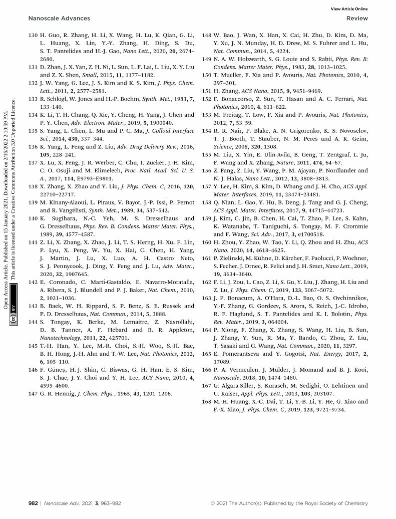
Nanoscale Advances Review
Ope
n A
cces
s A
rtic
le. P
ublis
hed
on 1
5 Ja
nuar
y 20
21. D
ownl
oade
d on
2/1
6/20
22 2
:10:
59 P
M.
Thi
s ar
ticle
is li
cens
ed u
nder
a C
reat
ive
Com
mon
s A
ttrib
utio
n 3.
0 U
npor
ted
Lic
ence
.View Article Online
130 H. Guo, R. Zhang, H. Li, X. Wang, H. Lu, K. Qian, G. Li,L. Huang, X. Lin, Y.-Y. Zhang, H. Ding, S. Du,S. T. Pantelides and H.-J. Gao, Nano Lett., 2020, 20, 2674–2680.
131 D. Zhan, J. X. Yan, Z. H. Ni, L. Sun, L. F. Lai, L. Liu, X. Y. Liuand Z. X. Shen, Small, 2015, 11, 1177–1182.
132 J. W. Yang, G. Lee, J. S. Kim and K. S. Kim, J. Phys. Chem.Lett., 2011, 2, 2577–2581.
133 R. Schlogl, W. Jones and H.-P. Boehm, Synth. Met., 1983, 7,133–140.
134 K. Li, T. H. Chang, Q. Xie, Y. Cheng, H. Yang, J. Chen andP. Y. Chen, Adv. Electron. Mater., 2019, 5, 1900040.
135 S. Yang, L. Chen, L. Mu and P.-C. Ma, J. Colloid InterfaceSci., 2014, 430, 337–344.
136 K. Yang, L. Feng and Z. Liu, Adv. Drug Delivery Rev., 2016,105, 228–241.
137 X. Lu, X. Feng, J. R. Werber, C. Chu, I. Zucker, J.-H. Kim,C. O. Osuji and M. Elimelech, Proc. Natl. Acad. Sci. U. S.A., 2017, 114, E9793–E9801.
138 X. Zhang, X. Zhao and Y. Liu, J. Phys. Chem. C, 2016, 120,22710–22717.
139 M. Kinany-Alaoui, L. Piraux, V. Bayot, J.-P. Issi, P. Pernotand R. Vangelisti, Synth. Met., 1989, 34, 537–542.
140 K. Sugihara, N.-C. Yeh, M. S. Dresselhaus andG. Dresselhaus, Phys. Rev. B: Condens. Matter Mater. Phys.,1989, 39, 4577–4587.
141 Z. Li, X. Zhang, X. Zhao, J. Li, T. S. Herng, H. Xu, F. Lin,P. Lyu, X. Peng, W. Yu, X. Hai, C. Chen, H. Yang,J. Martin, J. Lu, X. Luo, A. H. Castro Neto,S. J. Pennycook, J. Ding, Y. Feng and J. Lu, Adv. Mater.,2020, 32, 1907645.
142 E. Coronado, C. Martı-Gastaldo, E. Navarro-Moratalla,A. Ribera, S. J. Blundell and P. J. Baker, Nat. Chem., 2010,2, 1031–1036.
143 B. Baek, W. H. Rippard, S. P. Benz, S. E. Russek andP. D. Dresselhaus, Nat. Commun., 2014, 5, 3888.
144 S. Tongay, K. Berke, M. Lemaitre, Z. Nasrollahi,D. B. Tanner, A. F. Hebard and B. R. Appleton,Nanotechnology, 2011, 22, 425701.
145 T.-H. Han, Y. Lee, M.-R. Choi, S.-H. Woo, S.-H. Bae,B. H. Hong, J.-H. Ahn and T.-W. Lee, Nat. Photonics, 2012,6, 105–110.
146 F. Gunes, H.-J. Shin, C. Biswas, G. H. Han, E. S. Kim,S. J. Chae, J.-Y. Choi and Y. H. Lee, ACS Nano, 2010, 4,4595–4600.
147 G. R. Hennig, J. Chem. Phys., 1965, 43, 1201–1206.
982 | Nanoscale Adv., 2021, 3, 963–982
148 W. Bao, J. Wan, X. Han, X. Cai, H. Zhu, D. Kim, D. Ma,Y. Xu, J. N. Munday, H. D. Drew, M. S. Fuhrer and L. Hu,Nat. Commun., 2014, 5, 4224.
149 N. A. W. Holzwarth, S. G. Louie and S. Rabii, Phys. Rev. B:Condens. Matter Mater. Phys., 1983, 28, 1013–1025.
150 T. Mueller, F. Xia and P. Avouris, Nat. Photonics, 2010, 4,297–301.
151 H. Zhang, ACS Nano, 2015, 9, 9451–9469.152 F. Bonaccorso, Z. Sun, T. Hasan and A. C. Ferrari, Nat.
Photonics, 2010, 4, 611–622.153 M. Freitag, T. Low, F. Xia and P. Avouris, Nat. Photonics,
2012, 7, 53–59.154 R. R. Nair, P. Blake, A. N. Grigorenko, K. S. Novoselov,
T. J. Booth, T. Stauber, N. M. Peres and A. K. Geim,Science, 2008, 320, 1308.
155 M. Liu, X. Yin, E. Ulin-Avila, B. Geng, T. Zentgraf, L. Ju,F. Wang and X. Zhang, Nature, 2011, 474, 64–67.
156 Z. Fang, Z. Liu, Y. Wang, P. M. Ajayan, P. Nordlander andN. J. Halas, Nano Lett., 2012, 12, 3808–3813.
157 Y. Lee, H. Kim, S. Kim, D. Whang and J. H. Cho, ACS Appl.Mater. Interfaces, 2019, 11, 23474–23481.
158 Q. Nian, L. Gao, Y. Hu, B. Deng, J. Tang and G. J. Cheng,ACS Appl. Mater. Interfaces, 2017, 9, 44715–44723.
159 J. Kim, C. Jin, B. Chen, H. Cai, T. Zhao, P. Lee, S. Kahn,K. Watanabe, T. Taniguchi, S. Tongay, M. F. Crommieand F. Wang, Sci. Adv., 2017, 3, e1700518.
160 H. Zhou, Y. Zhao, W. Tao, Y. Li, Q. Zhou and H. Zhu, ACSNano, 2020, 14, 4618–4625.
161 P. Zielinski, M. Kuhne, D. Karcher, F. Paolucci, P. Wochner,S. Fecher, J. Drnec, R. Felici and J. H. Smet, Nano Lett., 2019,19, 3634–3640.
162 F. Li, J. Zou, L. Cao, Z. Li, S. Gu, Y. Liu, J. Zhang, H. Liu andZ. Lu, J. Phys. Chem. C, 2019, 123, 5067–5072.
163 J. P. Bonacum, A. O'Hara, D.-L. Bao, O. S. Ovchinnikov,Y.-F. Zhang, G. Gordeev, S. Arora, S. Reich, J.-C. Idrobo,R. F. Haglund, S. T. Pantelides and K. I. Bolotin, Phys.Rev. Mater., 2019, 3, 064004.
164 P. Xiong, F. Zhang, X. Zhang, S. Wang, H. Liu, B. Sun,J. Zhang, Y. Sun, R. Ma, Y. Bando, C. Zhou, Z. Liu,T. Sasaki and G. Wang, Nat. Commun., 2020, 11, 3297.
165 E. Pomerantseva and Y. Gogotsi, Nat. Energy, 2017, 2,17089.
166 P. A. Vermeulen, J. Mulder, J. Momand and B. J. Kooi,Nanoscale, 2018, 10, 1474–1480.
167 G. Algara-Siller, S. Kurasch, M. Sedighi, O. Lehtinen andU. Kaiser, Appl. Phys. Lett., 2013, 103, 203107.
168 M.-H. Huang, X.-C. Dai, T. Li, Y.-B. Li, Y. He, G. Xiao andF.-X. Xiao, J. Phys. Chem. C, 2019, 123, 9721–9734.
© 2021 The Author(s). Published by the Royal Society of Chemistry