
Electronic band structure and linear optical properties of paraelectric KIO 3
7
This content has been downloaded from IOPscience. Please scroll down to see the full text. Download details: IP Address: 130.18.123.11 This content was downloaded on 26/11/2013 at 16:34 Please note that terms and conditions apply. Electronic band structure and linear optical properties of paraelectric KIO 3 View the table of contents for this issue, or go to the journal homepage for more 2009 J. Phys.: Condens. Matter 21 125503 (http://iopscience.iop.org/0953-8984/21/12/125503) Home Search Collections Journals About Contact us My IOPscience
Transcript of Electronic band structure and linear optical properties of paraelectric KIO 3

This content has been downloaded from IOPscience. Please scroll down to see the full text.
Download details:
IP Address: 130.18.123.11
This content was downloaded on 26/11/2013 at 16:34
Please note that terms and conditions apply.
Electronic band structure and linear optical properties of paraelectric KIO3
View the table of contents for this issue, or go to the journal homepage for more
2009 J. Phys.: Condens. Matter 21 125503
(http://iopscience.iop.org/0953-8984/21/12/125503)
Home Search Collections Journals About Contact us My IOPscience
IOP PUBLISHING JOURNAL OF PHYSICS: CONDENSED MATTER
J. Phys.: Condens. Matter 21 (2009) 125503 (6pp) doi:10.1088/0953-8984/21/12/125503
Electronic band structure and linearoptical properties of paraelectric KIO3
Bahattin Erdinc1 and Harun Akkus
Physics Department, Yuzuncu Yil University, 65080 Van, Turkey
E-mail: [email protected]
Received 14 July 2008, in final form 3 December 2008Published 26 February 2009Online at stacks.iop.org/JPhysCM/21/125503
AbstractThe electronic energy band structure, partial (PDOS) and total density of states (DOS), andlinear optical properties of the paraelectric KIO3 single crystal are calculated using densityfunctional theory (DFT) in its local density approximation (LDA). The calculated bandstructure for paraelectric KIO3 indicates that the crystal has a direct bandgap. Using LDA andgeneralized gradient approximation (GGA), structural optimization has been performed. Theoptical spectra of the paraelectric KIO3 in the photon energy range up to 30 eV are investigatedunder the scissor approximation. The real and imaginary parts of the frequency-dependentlinear dielectric function, as well as related quantities such as energy-loss function, refractiveindex and effective number of valence electrons, are calculated. The calculated structuraloptimization and bandgap of the paraelectric KIO3 have been compared with experimental dataand have been found to be in good agreement with the experimental results.
1. Introduction
The materials having the chemical formula ABO3 have beenattractive for extensive investigations due to their interestingelectro-optic and electromechanical properties, nonlinearitiesand fundamental interest in the physics of their phasetransitions [1]. The perovskite compounds are on the listof ferroelectrics and they form an important group of theseingenious materials. The perovskite ferroelectric crystalshaving the chemical formula ABO3 are the most widelyknown and investigated ferroelectric materials because of thesimplicity of their crystal structures. They are criticallyimportant from a technological point of view. A large numberof perovskite ABO3 undergo a series of structural phasetransitions ranging from ferroelectric to antiferroelectric withthe change in temperature.
Potassium iodate, KIO3, single crystals have beeninvestigated extensively since 1961 [2, 3]. It transforms fromthe high temperature pseudocubic paraelectric phase to slightlydistorted ferroelectric phases with monoclinic and triclinicstructures [2]. KIO3 is an excellent nonlinear crystal [4, 5] andcan be used to fabricate nonlinear optical devices with goodoptical quality [6]. Therefore, the interest in nonlinear opticshas called attention to KIO3 as a possibly useful nonlinear
1 Author to whom any correspondence should be addressed.
optical material [7–9]. KIO3 undergoes successive phasetransitions with the temperature change. It has been reportedthat all phases, except phase I, are ferroelectric at atmosphericpressure. The phase transition temperatures are, respectively,T1 = 485 K (from phase I to phase II), T2 = 343 K (fromphase II to phase III), T3 = 255/263 K (on cooling/on heating)(from phase III to phase IV) and T4 = 83 K (from phase IVto phase V) [1]. In the paraelectric phase, phase I, the crystalhas a rhombohedral structure with space group R3m (Z = 1).In the first ferroelectric phase, phase II, it belongs to themonoclinic class with space group Pm (Z = 2). KIO3 singlecrystal has a triclinic structure with space group P1 (Z = 4) inphases III and IV [10]. However, we should emphasize thatKIO3 single-crystal structure has been variously reported ascubic, rhombohedral, monoclinic and triclinic. As far as weknow, in all reports to date, there has been no agreement onthe phase transitions and on the crystal structures in differentphases of KIO3. Most of these reports have been summarizedby Crane [11].
On the other hand, the phase transitions in the KIO3
have been studied in some detail. Liu et al have investigatedthe phase transition mechanism in KIO3 single crystals andhave calculated the phonon spectra of KIO3 in rhombohedralphase I, based on DEPT and LDA [10]. Yagi et alhave investigated the phase transitions using x-ray diffractionand EXAFS measurements to obtain additional structural
0953-8984/09/125503+06$30.00 © 2009 IOP Publishing Ltd Printed in the UK1
J. Phys.: Condens. Matter 21 (2009) 125503 B Erdinc and H Akkus
Table 1. Crystal structure data of paraelectric KIO3.
Atom Wyckoff x y z
Experiment [15] Space group R3m (160); cell parameter a = 4.4973 A
Atomic positions K 1a 0.511 17 0.511 17 0.511 17I 1a 0.000 00 0.000 00 0.000 00O 3b 0.028 04 0.028 04 −0.390 94
This work With only valenceelectrons
Space group R3m (160); cell parameter a = 4.5238 A
Atomic positions K 1a 0.561 12 0.561 12 0.561 12I 1a 0.020 57 0.020 57 0.020 57O 3b −0.021 04 −0.021 04 0.418 59
With valence plussemicore electrons
Space group R3m (160); cell parameter a = 4.6571 A
Atomic positions K 1a 0.573 34 0.573 34 0.573 34I 1a 0.018 65 0.018 65 0.018 65O 3b −0.024 42 −0.024 42 0.415 05
information [12]. Kasatani et al have measured the powderx-ray diffraction pattern of KIO3 in the wide temperaturerange from 100 to 530 K in order to determine the crystalstructure and clarify the mechanism of the successive phasetransitions of KIO3 crystals [13]. Kalinin et al performed thestructural analysis with single-crystal x-rays [14]. A single-crystal structural analysis for KIO3 has been said to be difficultby Kasatani et al, because of the ferroelectric and ferroelasticcomplicated domain of the structure [13]. Lucas studiedthe ferroelectric transition of KIO3 at the room temperaturephase using the neutron powder profile method to resolve thestructural uncertainty [15–17]. As far as we know, no ab initiogeneral potential calculations of the electronic band structureand optical properties of the ferroelectric phase III of KNO3
have been reported, in detail.The space group of rhombohedral KIO3 belongs to R3m,
and this crystal is reported to have one molecule in a unit celland the atomic positions in the unit cell are given in table 1.
In the present work, the paraelectric KIO3 single crystalhas been investigated using the pseudopotential method basedon the DFT under the LDA in the rhombohedral phase(phase I). First, the lattice parameters of the rhombohedralKIO3 crystal have been determined making the volumeoptimization by the LDA and the GGA using the localexperimental crystal structure data [15]. The electronicstructure and linear optical properties of the paraelectric KIO3
have been investigated. The calculated structural optimizationand bandgap of the paraelectric KIO3 are compared with theexperimental results.
2. Computational details
The self-consistent norm-conserving pseudopotentials for allatoms of KIO3 have been generated by using the FHI98PPcode [18] with a Troullier–Martins scheme [19]. To investigatethe effect of the pseudopotentials generated on the physicalproperties, especially on the bandgap width, two types ofpseudopotential were generated: for only valence electrons,and for valence electrons with semicore electrons. In the
first situation, for a potassium atom 4s electron, for iodineatom 5s and 5p electrons and for oxygen atom 2s and 2pelectrons; in the second, for potassium atom 3s, 3p and 4selectrons, for iodine atom 4d, 5s, and 5p electrons and foroxygen atom 2s and 2p electrons were considered as the truevalence, and the plane waves were used as the basis set forthe electronic wavefunctions. Ceperley–Alder Perdew–WangLDA functional (CAPW-LDA-92) [20] and Perdew–Burke–Ernzerhof GGA functional (PBE-GGA-96) [21] have beenused in order to take into account the exchange–correlationeffects in the procedure of the generation of pseudopotentials,and in all computations. In order to solve the Kohn–Sham equations [22], the conjugate gradient minimizationmethod [23] was employed by the ABINIT code [24]. Allthe calculations involve a five-atom rhombohedral unit cell.Good convergence for the bulk total energy calculation hasbeen achieved with the choice of cutoff energies at 45 Hartreeusing a 6 × 6 × 6 Monkhorst–Pack [25] mesh grid.
As is known, the Kohn–Sham equations determine theground-state properties. When the optical response calculationis made, thus the self-energy effects must be included.Otherwise the unoccupied conduction bands have no physicalsignificance and a bandgap problem appears: the absorptionstarts at too low an energy. In order to take into account theself-energy effects, the scissors approximation [26] has beenused and the scissor shift, to make the theoretical bandgapmatch the experimental one, has been chosen at 1 eV in thepresent work.
It is known that the dielectric function is mainly connectedwith the electronic response. The dielectric function wascalculated in the momentum representation, which requiresmatrix elements of the momentum �P between occupied andunoccupied eigenstates. The imaginary part ε′′(ω) of thedielectric function, ε(ω), is given by
ε′′(ω) = V e2
2π hm2ω2
∫d3k
∑n,n′
|〈�kn| �p|�kn′〉|2
× x f (�kn)(1 − f (�kn′))δ(E�kn − E�kn′ − hω), (1)
where e is the electron charge, m is the electron mass, V isthe volume, |�kn〉 is a crystal wavefunction, �p is the momentum
2
J. Phys.: Condens. Matter 21 (2009) 125503 B Erdinc and H Akkus
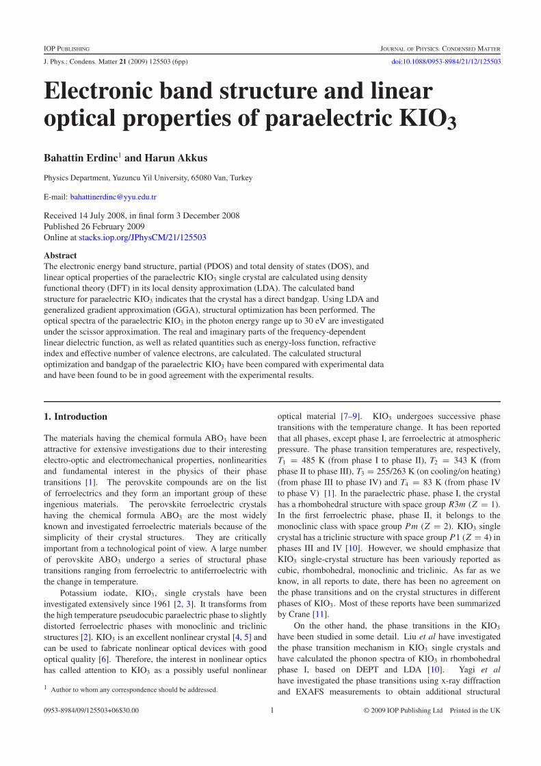
Figure 1. Dependence of total energy on unit cell volume of the rhombohedral KIO3 single crystal. (a) With only valence electrons and(b) with valence plus semicore electrons.
Table 2. Calculated and experimental lattice parameters, bandgaps and volumes of the rhombohedral KIO3.
This work Deviation (%)
With only valenceelectrons
With valence plussemicore electrons
With only valenceelectrons
With valence plussemicore electrons
GGA LDA GGA LDA Experiment GGA LDA GGA LDA
a (A) 4.6571 4.5238 4.7682 4.6571 4.4973 [15] 3.55 0.59 6.02 3.55
Volume (A3) 100.98 92.55 108.37 100.98 90.94 [15] 11.04 1.77 19.16 11.04
Bandgap (eV) 2.25 2.21 2.38 2.31 3–4.5 [1]
operator, f (�kn) is the Fermi function and hω is the energyof the incident photon. The summation over the Brillouinzone is a calculation using a linear interpolation on a meshof uniformly distributed points. Matrix elements, eigenvaluesand eigenvectors are calculated in the irreducible part of theBrillouin zone. The real part ε′(ω) of the dielectric functionε(ω) is evaluated from the imaginary part ε′′(ω) by theKramers–Kronig transformation. All other optical constantsof the energy dependence of refractive index n(ω), energy-loss spectrum L(ω) and effective number of valence electronsper unit cell, Neff, contributing in the interband transitions bymeans of the sum rule [27], can be derived from the real partε′(ω) of the dielectric function and the imaginary part ε′′(ω) ofthe dielectric function [28].
3. Results and discussion
3.1. Structural optimization
The geometric optimization of the unit cell has been performedfor a paraelectric KIO3 single crystal (phase I) using thecrystal structure data determined with the experimental latticeconstant (a = 4.4973 A) [15]. All physical properties arerelated to the total energy. For instance, the equilibrium latticeconstant of a crystal is the lattice constant that minimizes thetotal energy. If the total energy can be calculated, any physicalproperty which is related to the total energy can be determined.The lattice parameter of KIO3 is also obtained using thepseudopotential method based on the density functional theoryunder the local density approximation (LDA) and generalizedgradient approximation (GGA).
For two cases, both the pseudopotentials with only valenceelectrons and the pseudopotentials with the valence plussemicore electrons, geometric and atomic optimizations havebeen performed using both the LDA and GGA separately. Theobtained atomic positions are given in table 2. The computedlattice constant by minimizing the ratio of the total energy tothe volume for the two cases are given in table 2. The variationof the total energy as a function of the volume is presented infigure 1. As can be seen from table 2 and figure 1, geometricoptimization using the LDA is more acceptable than that usingthe GGA.
3.2. Band structure and density of states
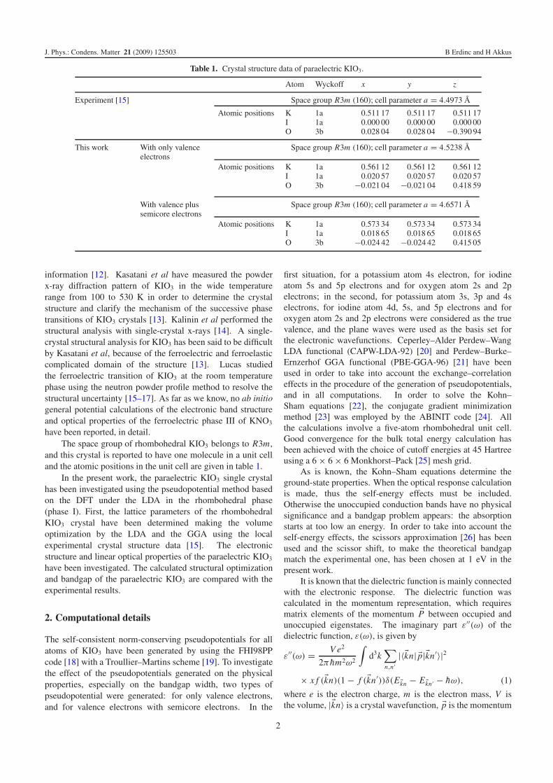
For a better understanding of the electronic and opticalproperties of KIO3, the investigation of electronic bandstructure can be useful. The calculated band structureof paraelectric KIO3 is shown in figure 2. The bandstructure has been computed and the high symmetry directionson the surface of the irreducible BZ plotted. The bandstructure calculations have been performed using two typesof pseudopotentials for the ingredient atoms of KIO3.However, figures 2 and 3 denote only computations inwhich pseudopotentials with valence plus semicore electronshave been used. It has been seen that the character ofthe band structure does not change with the choice ofpseudopotentials. However, the bandgap width changes withthe pseudopotentials used in the band structure calculations.The obtained bandgap values are given in table 2. In figure 2,the Fermi level is set to zero. The bottommost of the
3
J. Phys.: Condens. Matter 21 (2009) 125503 B Erdinc and H Akkus
Figure 2. Calculated band structure of the rhombohedral KIO3 singlecrystal.
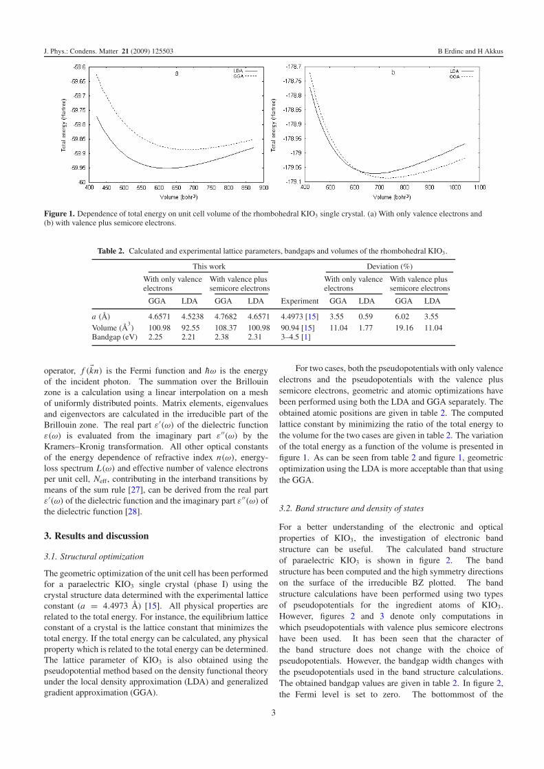
conduction band and the topmost of the valence band arelocated at the T point (1/2, 1/2, 1/2 in k-space) of the BZ.The bandgap values of the crystals like KIO3 are about 3–4.5 eV [1]. As can be seen from table 2, the calculatedbandgap of the paraelectric KIO3 can be compared with theexperimental results. The calculated bandgap is found to belower than the anticipated 3–4.5 eV range. The origin ofthis discrepancy may be the LDA which underestimates thebandgaps because of discontinuity in the exchange–correlationpotentials which is used in the calculations. The partial densityof states (PDOS) and total density of states (DOS) of theparaelectric KIO3 are investigated. The computed PDOS andDOS are shown in figure 3.
3.3. Optical properties
The optical properties of the paraelectric KIO3 are shown infigure 4. We have investigated real and imaginary parts ofthe frequency-dependent linear dielectric function, as well asrelated quantities such as energy-loss function, refractive indexand effective number of valence electrons of the KIO3 in theenergy range up to 30 eV. It is seen that a 0–30 eV photonenergy range is sufficient for the optical functions. Thus, wehave derived the values of the real and imaginary parts of thedielectric function as a function of the photon energy range upto 30 eV. Since the optical spectra have been analyzed for anenergy range 0–30 eV, the spectra contain a lot of peaks whichcorrespond to electronic transitions from the valence band tothe conduction band. The values of peaks of the imaginarypart of the frequency-dependent dielectric function which arelabeled with letters in figure 4 are summarized in table 3. KIO3
exhibits two fundamental oscillator bands at 4.66 and 6.49 eV,which correspond to the optical transitions from the valenceband to the conduction band. Analysis of figure 4 shows thatthe 0–4.5 eV photon energy range is characterized by hightransparency, no absorption and a small reflectivity.
The real part of the frequency-dependent linear dielectricfunction obtained from the imaginary part by Kramers–Kronigconversion is also presented in figure 3. The calculatedstatic dielectric constant for KIO3 is 4.01. The dielectric realfunction is equal to zero at 22.44 and 24.22 eV. The interbandtransitions at these points, which consist mostly of plasmonexcitations, the scattering probability of volume and surfacelosses are directly connected to the energy-loss function.
The calculated energy-loss functions, −Imε−1 for volumeand −Im(1 + ε)−1 for surface, are illustrated in figure 4.The energy-loss functions describe the energy loss of the fast
Figure 3. The partial density of states (PDOS) and total density of states (DOS) of the paraelectric KIO3.
4

J. Phys.: Condens. Matter 21 (2009) 125503 B Erdinc and H Akkus
Figure 4. Optical spectra for rhombohedral KIO3 single crystal.
Table 3. Comparative characteristics of the linear optical functions of the paraelectric KIO3 single crystal.
Peaks (eV)
A B C D E F G H I J K L M N O P
ε2 4.66 6.49 7.76 8.89 9.52 10.37 11.28 12.76 15.16 19.53 20.87 21.71 22.35 23.05 24.54 27.07
electrons transversing the material. The sharp maxima inthe energy-loss functions are associated with the existenceof plasma oscillations. The calculated energy-loss functionfor volume shows mainly sharp maxima peaks at 16.76 and25.24 eV. The peak value of volume loss, 25.24 eV, coincideswith the zero values of the real part of the dielectric function.The calculated energy-loss function for the surface showsmainly sharp peaks at 15.65 and 23.48 eV. As can be seenfrom figure 4, the sharp maxima in the energy-loss functionsare associated with the existence of plasma oscillations or theenergy of the volume and surface plasmon hωp.
Figure 4 also presents the spectral dependence of thecalculated main refractive index for a paraelectric KIO3 singlecrystal in a wide wavelength range. In order to calculate therefractive index, we have chosen a photon wavelength range of0–5 μm and have seen that a 0–5 μm photon wavelength rangeis sufficient for the refractive index. It is seen from the figurethat the refractive index decreases with the transition from theintrinsic absorption region towards long waves, i.e. a normaldispersion takes place. In the n = n(λ) dependence has beenobtained a maximum for λ = 0.319 μm. The maximum valueis n = 2.56.
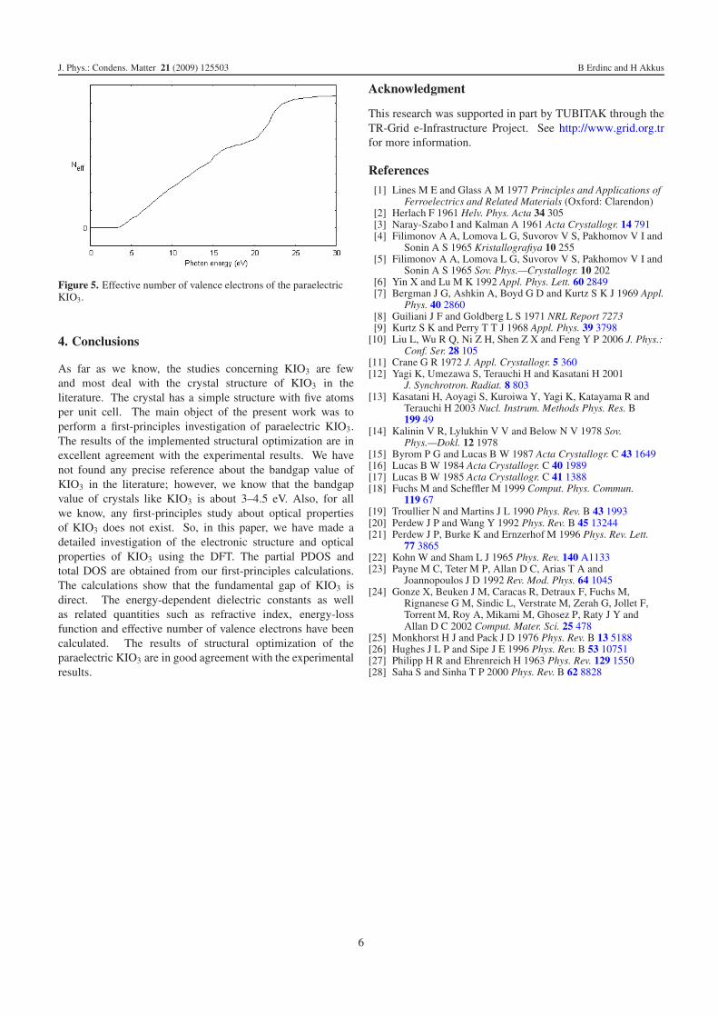
We have investigated the effective number of valenceelectrons of the KIO3 as a function of the photon energy inthe photon energy range up to 30 eV. The effective numberof valence electrons per unit cell contributing to the opticalconstants in the interband transitions can be calculated bymeans of the sum rule [27]. One can obtain an estimateof the distribution of oscillator strengths for both intrabandand interband transitions by computing the Neff(E0) definedaccording to
Neff(E0) = 2mε0
π h2e2
1
N0
∫ E0
0ε′′(E ′)E ′ dE ′, (2)
where Neff(E0) is the effective number of electronscontributing to optical transitions below an energy of E0. E0
denotes the upper limit of integration, the quantities m and eare the electron mass and charge, respectively, and N0 standsfor the electron density. As can be seen from figure 5, theeffective electron number, Neff(E0), up to 3.50 eV is zero, thenrises rapidly and reaches a saturation value above 27.50 eV.This shows that the deep-lying valence states do not participatein the interband transition.
5
J. Phys.: Condens. Matter 21 (2009) 125503 B Erdinc and H Akkus
Figure 5. Effective number of valence electrons of the paraelectricKIO3.
4. Conclusions
As far as we know, the studies concerning KIO3 are fewand most deal with the crystal structure of KIO3 in theliterature. The crystal has a simple structure with five atomsper unit cell. The main object of the present work was toperform a first-principles investigation of paraelectric KIO3.The results of the implemented structural optimization are inexcellent agreement with the experimental results. We havenot found any precise reference about the bandgap value ofKIO3 in the literature; however, we know that the bandgapvalue of crystals like KIO3 is about 3–4.5 eV. Also, for allwe know, any first-principles study about optical propertiesof KIO3 does not exist. So, in this paper, we have made adetailed investigation of the electronic structure and opticalproperties of KIO3 using the DFT. The partial PDOS andtotal DOS are obtained from our first-principles calculations.The calculations show that the fundamental gap of KIO3 isdirect. The energy-dependent dielectric constants as wellas related quantities such as refractive index, energy-lossfunction and effective number of valence electrons have beencalculated. The results of structural optimization of theparaelectric KIO3 are in good agreement with the experimentalresults.
Acknowledgment
This research was supported in part by TUBITAK through theTR-Grid e-Infrastructure Project. See http://www.grid.org.trfor more information.
References
[1] Lines M E and Glass A M 1977 Principles and Applications ofFerroelectrics and Related Materials (Oxford: Clarendon)
[2] Herlach F 1961 Helv. Phys. Acta 34 305[3] Naray-Szabo I and Kalman A 1961 Acta Crystallogr. 14 791[4] Filimonov A A, Lomova L G, Suvorov V S, Pakhomov V I and
Sonin A S 1965 Kristallografiya 10 255[5] Filimonov A A, Lomova L G, Suvorov V S, Pakhomov V I and
Sonin A S 1965 Sov. Phys.—Crystallogr. 10 202[6] Yin X and Lu M K 1992 Appl. Phys. Lett. 60 2849[7] Bergman J G, Ashkin A, Boyd G D and Kurtz S K J 1969 Appl.
Phys. 40 2860[8] Guiliani J F and Goldberg L S 1971 NRL Report 7273[9] Kurtz S K and Perry T T J 1968 Appl. Phys. 39 3798
[10] Liu L, Wu R Q, Ni Z H, Shen Z X and Feng Y P 2006 J. Phys.:Conf. Ser. 28 105
[11] Crane G R 1972 J. Appl. Crystallogr. 5 360[12] Yagi K, Umezawa S, Terauchi H and Kasatani H 2001
J. Synchrotron. Radiat. 8 803[13] Kasatani H, Aoyagi S, Kuroiwa Y, Yagi K, Katayama R and
Terauchi H 2003 Nucl. Instrum. Methods Phys. Res. B199 49
[14] Kalinin V R, Lylukhin V V and Below N V 1978 Sov.Phys.—Dokl. 12 1978
[15] Byrom P G and Lucas B W 1987 Acta Crystallogr. C 43 1649[16] Lucas B W 1984 Acta Crystallogr. C 40 1989[17] Lucas B W 1985 Acta Crystallogr. C 41 1388[18] Fuchs M and Scheffler M 1999 Comput. Phys. Commun.
119 67[19] Troullier N and Martins J L 1990 Phys. Rev. B 43 1993[20] Perdew J P and Wang Y 1992 Phys. Rev. B 45 13244[21] Perdew J P, Burke K and Ernzerhof M 1996 Phys. Rev. Lett.
77 3865[22] Kohn W and Sham L J 1965 Phys. Rev. 140 A1133[23] Payne M C, Teter M P, Allan D C, Arias T A and
Joannopoulos J D 1992 Rev. Mod. Phys. 64 1045[24] Gonze X, Beuken J M, Caracas R, Detraux F, Fuchs M,
Rignanese G M, Sindic L, Verstrate M, Zerah G, Jollet F,Torrent M, Roy A, Mikami M, Ghosez P, Raty J Y andAllan D C 2002 Comput. Mater. Sci. 25 478
[25] Monkhorst H J and Pack J D 1976 Phys. Rev. B 13 5188[26] Hughes J L P and Sipe J E 1996 Phys. Rev. B 53 10751[27] Philipp H R and Ehrenreich H 1963 Phys. Rev. 129 1550[28] Saha S and Sinha T P 2000 Phys. Rev. B 62 8828
6