
Electronic and Optoelectronic Properties of...
29
Electronic and Optoelectronic Properties of Semiconductor Structures Jasprit Singh University of Michigan, Ann Arbor
Transcript of Electronic and Optoelectronic Properties of...

Electronic and Optoelectronic Properties
of Semiconductor Structures
Jasprit Singh
University of Michigan, Ann Arbor

The Pitt Building, Trumpington Street, Cambridge, United Kingdom
The Edinburgh Building, Cambridge CB2 2RU, UK40 West 20th Street, New York, NY 10011–4211, USA477 Williamstown Road, Port Melbourne, VIC 3207, AustraliaRuiz de Alarcón 13, 28014 Madrid, SpainDock House, The Waterfront, Cape Town 8001, South Africa
http://www.cambridge.org
© Cambridge University Press 2003
This book is in copyright. Subject to statutory exceptionand to the provisions of relevant collective licensing agreements,no reproduction of any part may take place withoutthe written permission of Cambridge University Press.
First published 2003
Printed and bound by Williams Clowes Limited, Beccles and London
Typeset by the author
A catalogue record for this book is available from the British Library
ISBN 0 521 82379 X hardback

PREFACE
INTRODUCTION
I.1 SURVEY OF ADVANCES IN SEMICONDUCTORPHYSICS xiv
I.2 PHYSICS BEHIND SEMICONDUCTORS xvi
I.3 ROLE OF THIS BOOK xviii
STRUCTURAL PROPERTIESOF SEMICONDUCTORS
1.1 INTRODUCTION 1
1.2 CRYSTAL GROWTH 21.2.1 Bulk Crystal Growth 21.2.2 Epitaxial Crystal Growth 31.2.3 Epitaxial Regrowth 9
1.3 CRYSTAL STRUCTURE 101.3.1 Basic Lattice Types 121.3.2 Basic Crystal Structures 151.3.3 Notation to Denote Planes and Points in a Lattice:Miller Indices 161.3.4 Artificial Structures: Superlattices and Quantum Wells 211.3.5 Surfaces: Ideal Versus Real 221.3.6 Interfaces 231.3.7 Defects in Semiconductors 24
CONTENTS
xiii
xiv
1 1
1.4 STRAINED HETEROSTRUCTURES 26
1.5 STRAINED TENSOR IN LATTICE MISMATCHED EPITAXY 32
1.6 POLAR MATERIALS AND POLARIZATION CHARGE 35
1.7 TECHNOLOGY CHALLENGES 41
1.8 PROBLEMS 41
1.9 REFERENCES 44
SEMICONDUCTOR BANDSTRUCTURE
2.1 INTRODUCTION 46
2.2 BLOCH THEOREM AND CRYSTAL MOMENTUM 472.2.1 Significance of the k-vector 49
2.3 METALS, INSULATORS, AND SEMICONDUCTORS 51
2.4 TIGHT BINDING METHOD 542.4.1 Bandstructure Arising From a Single Atomic s-Level 572.4.2 Bandstructure of Semiconductors 60
2.5 SPIN-ORBIT COUPLING 622.5.1 Symmetry of Bandedge States 68
2.6 ORTHOGONALIZED PLANE WAVE METHOD 70
2.7 PSEUDOPOTENTIAL METHOD 71
2.8 k • p METHOD 74
2.9 SELECTED BANDSTRUCTURES 80
2.10 MOBILE CARRIERS: INTRINSIC CARRIERS 84
2.11 DOPING: DONORS AND ACCEPTORS 922.11.1 Carriers in Doped Semiconductors 952.11.2 Mobile Carrier Density and Carrier Freezeout 962.11.3 Equilibrium Density of Carriers in Doped Semiconductors 972.11.4 Heavily Doped Semiconductors 99
2.12 TECHNOLOGY CHALLENGES 102
2.13 PROBLEMS 104
2.14 REFERENCES 107
Contents
2 46
vi

BANDSTRUCTURE MODIFICATIONS
3.1 BANDSTRUCTURE OF SEMICONDUCTOR ALLOYS 1093.1.1 GaAs/AlAs Alloy 1133.1.2 InAs/GaAs Alloy 1133.1.3 HgTe/CdTe Alloy 1163.1.4 Si/Ge Alloy 1173.1.5 InN, GaN, AlN System 117
3.2 BANDSTRUCTURE MODIFICATIONS BY HETEROSTRUCTURES 1183.2.1 Bandstructure in Quantum Wells 1193.2.2 Valence Bandstructure in Quantum Wells 123
3.3 SUB-2-DIMENSIONAL SYSTEMS 124
3.4 STRAIN AND DEFORMATION POTENTIAL THEORY 1293.4.1 Strained Quantum Wells 1373.4.2 Self-Assembled Quantum Dots 140
3.5 POLAR HETEROSTRUCTURES 142
3.6 TECHNOLOGY ISSUES 145
3.7 PROBLEMS 145
3.8 REFERENCES 149
TRANSPORT: GENERAL FORMALISM
4.1 INTRODUCTION 152
4.2 BOLTZMANN TRANSPORT EQUATION 1534.2.1 Diffusion-Induced Evolution of fk(r) 1554.2.2 External Field-Induced Evolution of fk(r) 1564.2.3 Scattering-Induced Evolution of fk(r) 156
4.3 AVERAGING PROCEDURES 163
4.4 TRANSPORT IN A WEAK MAGNETIC FIELD: HALL MOBILITY 165
4.5 SOLUTION OF THE BOLTZMANN TRANSPORT EQUATION 1684.5.1 Iterative Approach 168
4.6 BALANCE EQUATION: TRANSPORT PARAMETERS 169
4.7 TECHNOLOGY ISSUES 175
4.8 PROBLEMS 176
4.9 REFERENCES 177
3 109
Contents vii
4 152

DEFECT AND CARRIER–CARRIER SCATTERING
5.1 IONIZED IMPURITY SCATTERING 181
5.2 ALLOY SCATTERING 191
5.3 NEUTRAL IMPURITY SCATTERING 194
5.4 INTERFACE ROUGHNESS SCATTERING 196
5.5 CARRIER–CARRIER SCATTERING 1985.5.1 Electron–Hole Scattering 1985.5.2 Electron–Electron Scattering: Scattering of Identical Particles
201
5.6 AUGER PROCESSES AND IMPACT IONIZATION 205
5.7 PROBLEMS 213
5.8 REFERENCES 214
LATTICE VIBRATIONS: PHONON SCATTERING
6.1 LATTICE VIBRATIONS 217
6.2 PHONON STATISTICS 2236.2.1 Conservation Laws in Scattering of Particles InvolvingPhonons 224
6.3 POLAR OPTICAL PHONONS 225
6.4 PHONONS IN HETEROSTRUCTURES 230
6.5 PHONON SCATTERING: GENERAL FORMALISM 231
6.6 LIMITS ON PHONON WAVEVECTORS 2376.6.1 Intravalley Acoustic Phonon Scattering 2386.6.2 Intravalley Optical Phonon Scattering 2396.6.3 Intervalley Phonon Scattering 240
6.7 ACOUSTIC PHONON SCATTERING 241
6.8 OPTICAL PHONONS: DEFORMATION POTENTIAL SCATTERING 243
6.9 OPTICAL PHONONS: POLAR SCATTERING 246
6.10 INTERVALLEY SCATTERING 251
Contentsviii
5 179
6 217

6.11 ELECTRON–PLASMON SCATTERING 252
6.12 TECHNOLOGY ISSUES 253
6.13 PROBLEMS 254
6.14 REFERENCES 257
VELOCITY-FIELD RELATIONSIN SEMICONDUCTORS
7.1 LOW FIELD TRANSPORT 261
7.2 HIGH FIELD TRANSPORT: MONTE CARLO SIMULATION 2647.2.1 Simulation of Probability Functions by Random Numbers 2657.2.2 Injection of Carriers 2667.2.3 Free Flight 2697.2.4 Scattering Times 2697.2.5 Nature of the Scattering Event 2717.2.6 Energy and Momentum After Scattering 272
7.3 STEADY STATE AND TRANSIENT TRANSPORT 2887.3.1 GaAs, Steady State 2887.3.2 GaAs, Transient Behavior 2907.3.3 High Field Electron Transport in Si 291
7.4 BALANCE EQUATION APPROACH TO HIGH FIELD TRANSPORT 292
7.5 IMPACT IONIZATION IN SEMICONDUCTORS 295
7.6 TRANSPORT IN QUANTUM WELLS 296
7.7 TRANSPORT IN QUANTUM WIRES AND DOTS 303
7.8 TECHNOLOGY ISSUES 305
7.9 PROBLEMS 306
7.10 REFERENCES 308
COHERENCE, DISORDER, ANDMESOSCOPIC SYSTEMS
8.1 INTRODUCTION 312
8.2 ZENER-BLOCH OSCILLATIONS 313
8.3 RESONANT TUNNELING 316
7 260
Contents ix
8 312

Contents
8.4 QUANTUM INTERFERENCE EFFECTS 323
8.5 DISORDERED SEMICONDUCTORS 3248.5.1 Extended and Localized States 3268.5.2 Transport in Disordered Semiconductors 328
8.6 MESOSCOPIC SYSTEMS 3348.6.1 Conductance Fluctuations and Coherent Transport 3358.6.2 Columb Blockade Effects 337
8.7 TECNOLOGY ISSUES 340
8.8 PROBLEMS 342
8.9 REFERENCES 343
OPTICAL PROPERTIES OF SEMICONDUCTORS
9.1 INTRODUCTION 345
9.2 MAXWELL EQUATIONS AND VECTOR POTENTIAL 346
9.3 ELECTRONS IN AN ELECTROMAGNETIC FIELD 351
9.4 INTERBAND TRANSITIONS 3589.4.1 Interband Transitions in Bulk Semiconductors 3589.4.2 Interband Transitions in Quantum Wells 361
9.5 INDIRECT INTERBAND TRANSITIONS 364
9.6 INTRABAND TRANSITIONS 3709.6.1 Intraband Transitions in Bulk Semiconductors 3719.6.2 Intraband Transitions in Quantum Wells 3719.6.3 Interband Transitions in Quantum Dots 374
9.7 CHARGE INJECTION AND RADIATIVE RECOMBINATION 3769.7.1 Spontaneous Emission Rate 3769.7.2 Gain in a Semiconductor 378
9.8 NONRADIATIVE RECOMBINATION 3819.8.1 Charge Injection: Nonradiative Effects 3819.8.2 Nonradiative Recombination: Auger Processes 382
9.9 SEMICONDUCTOR LIGHT EMITTERS 3859.9.1 Light Emitting Diode 3869.9.2 Laser Diode 387
9.10 CHARGE INJECTION AND BANDGAP RENORMALIZATION 395
9.11 TECHNOLOGY ISSUES 396
9 345
x

9.12 PROBLEMS 396
9.13 REFERENCES 400
EXCITONIC EFFECTS AND MODULATION OFOPTICAL PROPERTIES
10.1 INTRODUCTION 402
10.2 EXCITONIC STATES IN SEMICONDUCTORS 403
10.3 OPTICAL PROPERTIES WITH INCLUSION OF EXCITONIC EFFECTS 408
10.4 EXCITONIC STATES IN QUANTUM WELLS 413
10.5 EXCITONIC ABSORPTION IN QUANTUM WELLS 414
10.6 EXCITON BROADENING EFFECTS 416
10.7 MODULATION OF OPTICAL PROPERTIES 42010.7.1 Electro–Optic Effect 42110.7.2 Modulation of Excitonic Transitions:Quantum Confined Stark Effect 42610.7.3 Optical Effects in Polar Heterostructures 431
10.8 EXCITON QUENCHING 432
10.9 TECHNOLOGY ISSUES 434
10.10 PROBLEMS 436
10.11 REFERENCES 437
SEMICONDUCTORS IN MAGNETIC FIELDS
11.1 SEMICLASSICAL DYNAMICS OF ELECTRONSIN A MAGNETIC FIELD 44111.1.1 Semiclassical Theory of Magnetotransport 447
11.2 QUANTUM MECHANICAL APPROACH TO ELECTRONS
IN A MAGNETIC FIELD 451
11.3 AHARNOV-BOHM EFFECT 45711.3.1 Quantum Hall Effect 460
11.4 MAGNETO-OPTICS IN LANDAU LEVELS 465
11.5 EXCITONS IN MAGNETIC FIELD 467
10 402
Contents xi
44111

11.6 MAGNETIC SEMICONDUCTORS AND SPINTRONICS 46911.6.1 Spin Selection: Optical Injection 47011.6.2 Spin Selection: Electrical Injection and Spin Transistor 471
11.7 TECHNOLOGY ISSUES 474
11.8 PROBLEMS 474
11.9 REFERENCES 476
STRAIN IN SEMICONDUCTORS
A.1 ELASTIC STRAIN 478
A.2 ELASTIC CONSTANTS 480
EXPERIMENTAL TECHNIQUES
B.1 HIGH RESOLUTION X-RAY DIFFRACTION 484B.1.1 Double Crystal Diffraction 487
B.2 DRIFT MOBILITY AND HALL MOBILITY 487B.2.1 Haynes-Schockley Experiment 488B.2.2 Hall Effect for Carrier Density and Hall Mobility 490
B.3 PHOTOLUMINESCENCE (PL) AND EXCITATIONPHOTOLUMINESCENCE (PLE) 490
B.4 OPTICAL PUMP PROBE EXPERIMENTS 494
QUANTUM MECHANICS: USEFUL CONCEPTS
C.1 DENSITY OF STATES 499
C.2 STATIONARY PERTURBATION THEORY 504C.2.1 Nondegenerate Case 504C.2.2 Degenerate Case 507
C.3 TIME DEPENDENT PERTURBATION THEORY AND FERMIGOLDEN RULE 509
C.4 BOUND STATE PROBLEM: MATRIX TECHNIQUES 511
IMPORTANT PROPERTIES OF SEMICONDUCTORS
INDEX
Contentsxii
A 478
B 484
C 498
D 514
527

Chapter
1
STRUCTURALPROPERTIES OF
SEMICONDUCTORS
1.1 INTRODUCTION
Semiconductors form the basis of most modern information processing devices. Elec-tronic devices such as diodes, bipolar junction transistors, and field effect transistorsdrive modern electronic technology. Optoelectronic devices such as laser diodes, modu-lators, and detectors drive the optical networks. In addition to devices, semiconductorstructures have provided the stages for exploring questions of fundamental physics.Quantum Hall effect and other phenomena associated with many-body effects and lowdimensions have been studied in semiconductor structures.
It is important to recognize that the ability to examine fundamental physicsissues and to use semiconductors in state of the art device technologies depends crit-ically on the purity and perfection of the semiconductor crystal. Semiconductors areoften associated with clean rooms and workers clad in “bunny suits” lest the tinieststray particle get loose and latch onto the wafer being processed. Indeed, semiconductorstructures can operate at their potential only if they can be grown with a high de-gree of crystallinity and if impurities and defects can be controlled. For high structuralquality it is essential that a high quality substrate be available. This requires growthof bulk crystals which are then sliced and polished to allow epitaxial growth of thinsemiconductor regions including heterostructures.
In this chapter we start with a brief discussion of the important bulk and epi-taxial crystal growth techniques. We then discuss the important semiconductor crystalstructures. We also discuss strained lattice structures and the strain tensor for suchcrystals. Strained epitaxy and its resultant consequences are now widely exploited in

2 Chapter 1. Structural Properties of Semiconductors
semiconductor physics and it is important to examine how epitaxial growth causes dis-tortions in the crystal lattice.
1.2 CRYSTAL GROWTH
1.2.1 Bulk Crystal GrowthSemiconductor technology depends critically upon the availability of high quality sub-strates with as large a diameter as possible. Bulk crystal growth techniques are usedmainly to produce substrates on which devices are eventually fabricated. While for somesemiconductors like Si and GaAs (to some extent for InP) the bulk crystal growth tech-niques are highly matured; for most other semiconductors it is difficult to obtain highquality, large area substrates. Several semiconductor technologies are dependent on sub-strates that are not ideal. For example, the nitrides GaN, AlN, InN are grown on SiCor sapphire substrates, since there is no reliable GaN substrate. The aim of the bulkcrystal growth techniques is to produce single crystal boules with as large a diameter aspossible and with as few defects as possible. In Si the boule diameters have reached 30cm with boule lengths approaching 100 cm. Large size substrates ensure low cost deviceproduction.
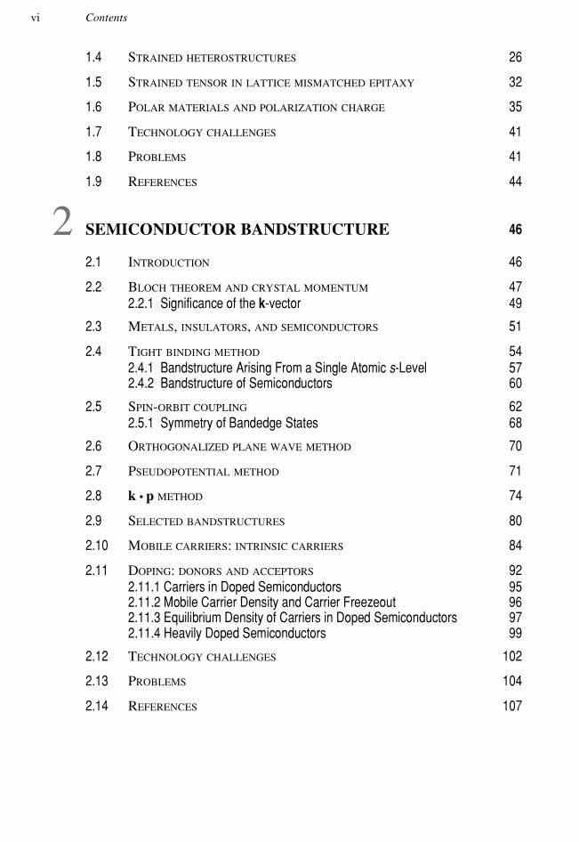
For the growth of boules from which substrates are obtained, one starts outwith a purified form of the elements that are to make up the crystal. One importanttechnique that is used is the Czochralski (CZ) technique. In the Czochralski techniqueshown in Fig. 1.1, the melt of the charge (i.e., the high quality polycrystalline material)is held in a vertical crucible. The top surface of the melt is just barely above the meltingtemperature. A seed crystal is then lowered into the melt and slowly withdrawn. As theheat from the melt flows up the seed, the melt surface cools and the crystal beginsto grow. The seed is rotated about its axis to produce a roughly circular cross-sectioncrystal. The rotation inhibits the natural tendency of the crystal to grow along certainorientations to produce a faceted crystal.
The CZ technique is widely employed for Si, GaAs, and InP and produces longingots (boules) with very good circular cross-section. For Si up to 100 kg ingots can beobtained. In the case of GaAs and InP the CZ technique has to face problems arisingfrom the very high pressures of As and P at the melting temperature of the compounds.Not only does the chamber have to withstand such pressures, also the As and P leavethe melt and condense on the sidewalls. To avoid the second problem one seals the meltby covering it with a molten layer of a second material (e.g., boron oxide) which floatson the surface. The technique is then referred to as liquid encapsulated Czochralski, orthe LEC technique.
A second bulk crystal growth technique involves a charge of material loaded ina quartz container. The charge may be composed of either high quality polycrystallinematerial or carefully measured quantities of elements which make up a compound crys-tal. The container called a “boat” is heated till the charge melts and wets the seedcrystal. The seed is then used to crystallize the melt by slowly lowering the boat tem-perature starting from the seed end. In the gradient-freeze approach the boat is pushedinto a furnace (to melt the charge) and slowly pulled out. In the Bridgeman approach,the boat is kept stationary while the furnace temperature is temporally varied to form
1.2. Crystal Growth 3
Melt
Crystal
Puller
Seed
Heater
View-port
Encapsulant
Figure 1.1: Schematic of Czochralski-style crystal grower used to produce substrate ingots.The approach is widely used for Si, GaAs and InP.
the crystal. The approaches are schematically shown in Fig. 1.2.The easiest approach for the boat technique is to use a horizontal boat. However,
the shape of the boule that is produced has a D-shaped form. To produce circular cross-sections vertical configurations have now been developed for GaAs and InP.
In addition to producing high purity bulk crystals, the techniques discussedabove are also responsible for producing crystals with specified electrical properties.This may involve high resistivity materials along with n- or p-type materials. In Si it isdifficult to produce high resistivity substrated by bulk crystal growth and resistivities areusually <104 Ω-cm. However, in compound semiconductors carrier trapping impuritiessuch as chromium and iron can be used to produce material with resistivities of ∼ 108 Ωcm. The high resistivity or semi-insulating (SI) substrates are extremely useful in deviceisolation and for high speed devices. For n- or p-type doping carefully measured dopantsare added in the melt.
1.2.2 Epitaxial Crystal Growth
Once bulk crystals are grown, they are sliced into substrates or wafers about 250 µmthick. These are polished and used for growth of epitaxial layers a few micrometersthick. All active devices are produced on these epitaxial layers. As a result the epi-taxial growth techniques are very important. The epitaxial growth techniques have avery slow growth rate (as low as a monolayer per second for some techniques) whichallow one to control very accurately the dimensions in the growth direction. In fact,in techniques like molecular beam epitaxy (MBE) and metal organic chemical vapor

4 Chapter 1. Structural Properties of Semiconductors
Furnace tube Heater
Seed
Molten material
CrystalCrucible Seed
Crystal
PolycrystalMolten zone
(a) (b)
PullPull
Figure 1.2: Crystal growing from the melt in a crucible: (a) solidification from one end of themelt (horizontal Bridgeman method); (b) melting and solidification in a moving zone.
deposition (MOCVD), one can achieve monolayer (∼ 3 A) control in the growth direc-tion. This level of control is essential for the variety of heterostructure devices that arebeing used in optoelectronics. The epitaxial techniques are also very useful for precisedoping profiles that can be achieved. In fact, it may be argued that without the ad-vances in epitaxial techniques that have occurred over the last two decades, most of thedevelopments in semiconductor physics would not have occurred. Table 1.1 gives a briefview of the various epitaxial techniques used along with some of the advantages anddisadvantages.
Liquid Phase Epitaxy (LPE)LPE is a relatively simple epitaxial growth technique which was widely used until 1970swhen it gradually gave way to approaches such as MBE and MOCVD. It is a less ex-pensive technique (compared to MBE or MOCVD), but it offers less control in interfaceabruptness when growing heterostructures. LPE is still used for growth of crystals suchas HgCdTe for long wavelength detectors and AlGaAs for double heterostructure lasers.As shown in Table 1.1, LPE is a close to equilibrium technique in which the substrate isplaced in a quartz or a graphite boat and covered by a liquid of the crystal to be grown(see Fig. 1.3). The liquid may also contain dopants that are to be introduced into thecrystal. LPE is often used for alloy growth where the growth follows the equilibriumsolid-liquid phase diagram. By precise control of the liquid composition and tempera-ture, the alloy composition can be controlled. Because LPE is a very close to equilibriumgrowth technique, it is difficult to grow alloy systems which are not miscible or evengrow heterostructures with atomically abrupt interfaces. Nevertheless heterostructureswhere interface is graded over 10-20 A can be grown by LPE by sliding the boat oversuccessive “puddles” of different semiconductors. For many applications such interfacesare adequate and since LPE is a relatively inexpensive growth technique, it is used inmany commercial applications.
Vapor Phase Epitaxy (VPE)A large class of epitaxial techniques rely on delivering the components that form thecrystal from a gaseous environment. If one has molecular species in a gaseous form with

1.2. Crystal Growth 5
PullGaAs melt
AlGaAs melt
GaAs substrate
Slider
Figure 1.3: A schematic of the LPE growth of AlGaAs and GaAs. The slider moves the sub-strate, thus positioning itself to achieve contact with the different melts to grow heterostruc-tures.
LIQUID PHASE
EPITAXY
Relativelyinexpensive
Difficult togrow abruptheterostructures
Unable to growimmiscible alloys
Near equilibriumgrowth for precisealloy compositions
Very highqualitymaterial
MBE
High quality materials
Atomically abruptinterfaces
Techniques can growfar from equilibriumsystems reliably
"Expensive" growthtechnology whichrequires great care
Not wellsuited forheterostructures
Extremelyhigh puritymaterial
VAPOR PHASE
EPITAXY
+
+
+
−
−
+
−
+
+
+
−
MOCVD
MOMBE
Table 1.1: A schematic of the various epitaxial crystal growth techniques and some of theirpositive and negative aspects.

6 Chapter 1. Structural Properties of Semiconductors
Substrates
Substrateholder
Substrates
Heater lamps
VERTICAL REACTOR HORIZONTAL REACTOR
Substrate holder
Figure 1.4: Reactors for VPE growth. The substrate temperature must be maintained uni-formly over the area. This is achieved better by lamp heating. A pyrometer is used for temper-ature measurement.
partial pressure P , the rate at which molecules impinge upon a substrate is given by
F =P√
2πmkBT∼ 3.5 × 10²²P (torr)√
m(g)T (K)mol./cm2s (1.1)
where m is the molecular weight and T the cell temperature. For most crystals thesurface density of atoms is ∼ 7 × 1014 cm−2. If the atoms or molecules impinging fromthe vapor can be deposited on the substrate in an ordered manner, epitaxial crystalgrowth can take place.
The VPE technique is used mainly for homoepitaxy and does not have theadditional apparatus present in techniques such as MOCVD for precise heteroepitaxy.As an example of the technique, consider the VPE of Si. The Si containing reactant silane(SiH4) or dichlorosilane (SiH2Cl2) or trichlorosilane (SiHCl3) or silicon tetrachloride(SiCl4) is diluted in hydrogen and introduced into a reactor in which heated substratesare placed as shown in Fig. 1.4. The silane pyrolysis to yield silicon while the chlorinecontaining gases react to give SiCl2, HCl and various other silicon-hydrogen-chlorinecompounds. The reaction
2SiCl2 Si + SiCl4 (1.2)
then yields Si. Since HCl is also produced in the reaction, conditions must be tailored sothat no etching of Si occurs by the HCl. Doping can be carried out by adding appropriatehydrides (phosphine, arsine, etc.,) to the reactants.
VPE can be used for other semiconductors as well by choosing different ap-propriate reactant gases. The reactants used are quite similar to those employed in theMOCVD technique discussed later.
Molecular Beam Epitaxy (MBE)MBE is capable of controlling deposition of submonolayer coverage on a substrate andhas become one of the most important epitaxial techniques. Almost every semiconductor

1.2. Crystal Growth 7
To variable speedmotor and substrate
heater supply
Rheed gun
Rotating substrateholder
Ionization gauge
Gate valve
Sample exchangeload lock
Viewport
Sapphireviewport
Effusion cellshutters
Fluorescentscreen
Photomultiplier
Liquid nitrogencooled shrouds
Figure 1.5: A schematic of the MBE growth system.
has been grown by this technique. MBE is a high vacuum technique (∼ 10−11 torrvacuum when fully pumped down) in which crucibles containing a variety of elementalcharges are placed in the growth chamber (Fig. 1.5). The elements contained in thecrucibles make up the components of the crystal to be grown as well as the dopantsthat may be used. When a crucible is heated, atoms or molecules of the charge areevaporated and these travel in straight lines to impinge on a heated substrate.
The growth rate in MBE is ∼1.0 monolayer per second and this slow ratecoupled with shutters placed in front of the crucibles allow one to switch the compositionof the growing crystal with monolayer control. Since no chemical reactions occur inMBE, the growth is the simplest of all epitaxial techniques and is quite controllable.However, since the growth involves high vacuum, leaks can be a major problem. Thegrowth chamber walls are usually cooled by liquid N2 to ensure high vacuum and toprevent atoms/molecules to come off from the chamber walls.
The low background pressure in MBE allows one to use electron beams tomonitor the growing crystal. The reflection high energy electron diffraction (RHEED)techniques relies on electron diffraction to monitor both the quality of the growingsubstrate and the layer by layer growth mode.

8 Chapter 1. Structural Properties of Semiconductors
Metal Organic Chemical Vapor Deposition (MOCVD)Metal organic chemical vapor deposition (MOCVD) is another important growth tech-nique widely used for heteroepitaxy. Like MBE, it is also capable of producing monolayerabrupt interfaces between semiconductors. A typical MOCVD system is shown in Fig.1.6. Unlike in MBE, the gases that are used in MOCVD are not made of single elements,but are complex molecules which contain elements like Ga or As to form the crystal.Thus the growth depends upon the chemical reactions occurring at the heated substratesurface. For example, in the growth of GaAs one often uses triethyl gallium and arsineand the crystal growth depends upon the following reaction:
Ga(CH3)3 + AsH3 GaAs + 3CH4 (1.3)
One advantage of the growth occurring via a chemical reaction is that one canuse lateral temperature control to carry out local area growth. Laser assisted local areagrowth is also possible for some materials and can be used to produce new kinds ofdevice structures. Such local area growth is difficult in MBE.
There are several varieties of MOCVD reactors. In the atmospheric MOCVDthe growth chamber is essentially at atmospheric pressure. One needs a large amount ofgases for growth in this case, although one does not have the problems associated withvacuum generation. In the low pressure MOCVD the growth chamber pressure is keptlow. The growth rate is then slower as in the MBE case.
The use of the MOCVD equipment requires very serious safety precautions. Thegases used are highly toxic and a great many safety features have to be incorporatedto avoid any deadly accidents. Safety and environmental concerns are important issuesin almost all semiconductor manufacturing since quite often one has to deal with toxicand hazardous materials.
In addition to MBE and MOCVD one has hybrid epitaxial techniques oftencalled MOMBE (metal organic MBE) which try to combine the best of MBE andMOCVD. In MBE one has to open the chamber to load the charge for the materials tobe grown while this is avoided in MOCVD where gas bottles can be easily replaced fromoutside. Additionally, in MBE one has occasional spitting of material in which smallclumps of atoms are evaporated off on to the substrate. This is avoided in MOCVD andMOMBE.
EXAMPLE 1.1 Consider the growth of GaAs by MBE. The Ga partial pressure in thegrowth chamber is 10−5 Torr, and the Ga cell temperature is 900 K. Calculate the flux of Gaatoms on the substrate. The surface density of Ga atoms on GaAs grown along (001) directionis 6.3×1014 cm−2. Calculate the growth rate if all of the impinging atoms stick to the substrate.
The mass of Ga atoms is 70 g/mole. The flux is (from Eqn. 1.1)
F =3.5 × 1022 × 10−5
√70 × 900
= 5.27 × 10¹⁴atoms/cm2
Note that the surface density of Ga atoms on GaAs is ∼ 6.3 × 1014 cm−2. Thus, if all of the
Ga atoms were to stick, the growth rate would be ∼0.8 monolayer per second. This assumes
that there is sufficient arsenic to provide As in the crystal. This is a typical growth rate for
epitaxial films. It would take nearly 10 hours to grow a 10 µm film.

1.2. Crystal Growth 9
GaAs
Mass-flowcontrollers
TMGa
TMAl
H2
Growth line
AsH3
Dopant
Mass-flowVent line
Heatedwafer
Exhaust line
Scrubber
Exhaust
TMGa : Gallium containing organic compoundTMAl : Aluminum containing organic compoundAsH3 : Arsenic containing compound
Chemical reaction at the heatedsubstrate deposits GaAs or AlAs.Mass flow controllers control thespecies deposited.
Figure 1.6: Schematic diagram of an MOCVD system employing alkyds (trimethyl gallium(TMGa) and trimethyl aluminum (TMAl) and metal hydride (arsine) material sources, withhydrogen as a carrier gas.
1.2.3 Epitaxial Regrowth
The spectacular growth of semiconductor microelectronics owes a great deal to theconcept of the integrated circuit. The ability to fabricate transistors, resistors, inductorsand capacitors on the same wafer is critical to the low cost and high reliability we havecome to expect from microelectronics. It is natural to expect similar dividents from theconcept of the optoelectronic integrated circuit (OEIC). In the OEIC, the optoelectronicdevice (the laser or detector or modulator) would be integrated on the same wafer withan amplifier or logic gates.
One of the key issues in OEICs involves etching and regrowth. As we will see

10 Chapter 1. Structural Properties of Semiconductors
later, the optoelectronic devices have a structure that is usually not compatible withthe structure of an electronic device. The optimum layout then involves growing oneof the device structures epitaxially and then masking the region to be used as, say,the optoelectronic device and etching away the epitaxial region. Next a regrowth isdone to grow the electronic device with a different structure. The process is shownschematically in Fig. 1.7. While this process looks simple conceptually, there are seriousproblems associated with etching and regrowth.
A critical issue in the epitaxial growth of a semiconductor layer is the quality ofthe semiconductor-vacuum interface. This semiconductor surface must be “clean,” i.e.,there should be no impurity layers (e.g., an oxide layer) on the surface. Even if a fractionof a monolayer of the surface atoms have impurities bonded to them, the quality of theepitaxial layer suffers drastically. The growth may occur to produce microcrystallineregions separated by grain boundaries or may be amorphous in nature. In either case,the special properties arising from the crystalline nature of the material (to be discussedin the next chapter) are then lost.
The issue of surface cleanliness and surface reconstruction can be addressedwhen one is doing a single epitaxial growth. For example, a clean wafer can be loadedinto the growth chamber and the remaining impurities on the surface can be removed byheating the substrate. The proper reconstruction (which can be monitored by RHEED)can be ensured by adjusting the substrate temperature and specy overpressure. Nowconsider the problems associated with etching after the first epitaxial growth has oc-curred. As the etching starts, foreign atoms or molecules are introduced on the wafer asthe semiconductor is etched. The etching process is quite damaging and as it ends, thesurface of the etched wafer is quite rough and damaged. In addition, in most growthtechniques the wafer has to be physically moved from the high purity growth chamberto the etching system. During this transportation, the surface of the wafer may collectsome “dirt.” During the etching process this “dirt” may not be etched off and mayremain on the wafer. As a result of impurities and surface damage, when the secondepitaxial layer is grown after etching, the quality of the layer suffers.
A great deal of processing research in OEICs focusses on improving the etch-ing/regrowth process. So far the OEICs fabricated in various laboratories have perfor-mances barely approaching the performance of hybrid circuits. Clearly the problem ofetching/regrowth is hampering the progress in OEIC technology.
It may be noted that the etching regrowth technology is also important increating quantum wires and quantum dots which require lateral patterning of epitaxiallayers.
1.3 CRYSTAL STRUCTUREEssentially all high performance semiconductor devices are based on crystalline mate-rials. there are some devices that use low cast amorphous or polycrystalline semicon-ductors, but their performance is quite poor. Crystals are made up of identical buildingblocks, the block being an atom or a group of atoms. While in “natural” crystals thecrystalline symmetry is fixed by nature, new advances in crystal growth techniquesare allowing scientists to produce artificial crystals with modified crystalline structure.

1.3. Crystal Structure 11
Structure of the electronic device Structure of the optoelectronic device
Desired OEIC
Substrate
Substrate
APPROACH
Growth of the optoelectronic device structure
Mask a portion of the layer
Etch backRegrowth of the electronic device structure
OEIC
Figure 1.7: The importance of regrowth is clear when one examines the difference in the struc-ture of electronic and optoelectronic devices. Etching and regrowth is essential for fabricationof optoelectronic integrated circuits (OEIC).
These advances depend upon being able to place atomic layers with exact precision andcontrol during growth, leading to “superlattices”. To define the crystal structure, twoimportant concepts are introduced. The lattice represents a set of points in space whichform a periodic structure. Each point sees an exact similar environment. The lattice isby itself a mathematical abstraction. A building block of atoms called the basis is thenattached to each lattice point yielding the crystal structure.
An important property of a lattice is the ability to define three vectors a1, a2,a3, such that any lattice point R′ can be obtained from any other lattice point R by atranslation
R′ = R+ m1a1 + m2a2 + m3a3 (1.4)

12 Chapter 1. Structural Properties of Semiconductors
where m1, m2, m3 are integers. Such a lattice is called Bravais lattice. The entire latticecan be generated by choosing all possible combinations of the integers m1, m2, m3 .The crystalline structure is now produced by attaching the basis to each of these latticepoints.
lattice + basis = crystal structure (1.5)
The translation vectors a1, a2, and a3 are called primitive if the volume of the cellformed by them is the smallest possible. There is no unique way to choose the primitivevectors. One choice is to pick
a1 to be the shortest period of the latticea2 to be the shortest period not parallel to a1
a3 to be the shortest period not coplanar with a1 and a2
It is possible to define more than one set of primitive vectors for a given lat-tice, and often the choice depends upon convenience. The volume cell enclosed by theprimitive vectors is called the primitive unit cell.
Because of the periodicity of a lattice, it is useful to define the symmetry of thestructure. The symmetry is defined via a set of point group operations which involvea set of operations applied around a point. The operations involve rotation, reflectionand inversion. The symmetry plays a very important role in the electronic propertiesof the crystals. For example, the inversion symmetry is extremely important and manyphysical properties of semiconductors are tied to the absence of this symmetry. As willbe clear later, in the diamond structure (Si, Ge, C, etc.), inversion symmetry is present,while in the Zinc Blende structure (GaAs, AlAs, InAs, etc.), it is absent. Because ofthis lack of inversion symmetry, these semiconductors are piezoelectric, i.e., when theyare strained an electric potential is developed across the opposite faces of the crystal. Incrystals with inversion symmetry, where the two faces are identical, this is not possible.
1.3.1 Basic Lattice TypesThe various kinds of lattice structures possible in nature are described by the symmetrygroup that describes their properties. Rotation is one of the important symmetry groups.Lattices can be found which have a rotation symmetry of 2π, 2π
2 , 2π3 , 2π
4 , 2π6 . The rotation
symmetries are denoted by 1, 2, 3, 4, and 6. No other rotation axes exist; e.g., 2π5 or 2π
7are not allowed because such a structure could not fill up an infinite space.
There are 14 types of lattices in 3D. These lattice classes are defined by therelationships between the primitive vectors a1, a2, and a3, and the angles α, β, andγ between them. The general lattice is triclinic (α = β = γ, a1 = a2 = a3) and thereare 13 special lattices. Table 1.2 provides the basic properties of these three dimen-sional lattices. We will focus on the cubic lattice which is the structure taken by allsemiconductors.
There are 3 kinds of cubic lattices: simple cubic, body centered cubic, and facecentered cubic.

1.3. Crystal Structure 13
Number Restrictions onof conventional cell axes
System lattices and singlesTriclinic 1 a1 = a2 = a3
α = β = γMonoclinic 2 a1 = a2 = a3
α = γ = 90o = βOrthorhombic 4 a1 = a2 = a3
α = β = γ = 90o
Tetragonal 2 a1 = a2 = a3
α = β = γ = 90o
Cubic 3 a1 = a2 = a3
α = β = γ = 90o
Trigonal 1 a1 = a2 = a3
α = β = γ < 120o, = 90o
Hexagonal 1 a1 = a2 = a3
α = β = 90o
γ = 120o
Table 1.2: The 14 Bravais lattices in 3-dimensional systems and their properties.
x
y
z
a3
a2
a1a
Figure 1.8: A simple cubic lattice showing the primitive vectors. The crystal is produced byrepeating the cubic cell through space.

14 Chapter 1. Structural Properties of Semiconductors
a3
a2a1
Figure 1.9: The body centered cubic lattice along with a choice of primitive vectors.
Simple cubic: The simple cubic lattice shown in Fig. 1.8 is generated by the primitivevectors
ax, ay, az (1.6)
where the x, y, z are unit vectors.
Body-centered cubic: The bcc lattice shown in Fig. 1.9 can be generated from thesimple cubic structure by placing a lattice point at the center of the cube. If x, y, and zare three orthogonal unit vectors, then a set of primitive vectors for the body-centeredcubic lattice could be
a1 = ax, a2 = ay, a3 =a
2(x+ y + z) (1.7)
A more symmetric set for the bcc lattice is
a1 =a
2(y + z− x), a2 =
a
2(z+ x− y), a3 =
a
2(x+ y − z) (1.8)
Face Centered Cubic: Another equally important lattice for semiconductors is theface-centered cubic (fcc) Bravais lattice. To construct the face-centered cubic Bravaislattice add to the simple cubic lattice an additional point in the center of each squareface (Fig. 1.10).
A symmetric set of primitive vectors for the face-centered cubic lattice (see Fig.1.10) is
a1 =a
2(y + z), a2 =
a
2(z + x), a3 =
a
2(x + y) (1.9)
The face-centered cubic and body-centered cubic Bravais lattices are of greatimportance, since an enormous variety of solids crystallize in these forms with an atom(or ion) at each lattice site. Essentially all semiconductors of interest for electronics andoptoelectronics have fcc structure.

1.3. Crystal Structure 15
z
y
x
a3
a2a1
a
fcc lattice
Figure 1.10: Primitive basis vectors for the face centered cubic lattice.
1.3.2 Basic Crystal StructuresDiamond and Zinc Blende StructuresMost semiconductors of interest for electronics and optoelectronics have an underlyingfcc lattice. However, they have two atoms per basis. The coordinates of the two basisatoms are
(000) and (a
4,a
4,a
4) (1.10)
Since each atom lies on its own fcc lattice, such a two atom basis structure may bethought of as two inter-penetrating fcc lattices, one displaced from the other by a trans-lation along a body diagonal direction (a4
a4a4 ).
Figure 1.11 gives details of this important structure. If the two atoms of thebasis are identical, the structure is called diamond. Semiconductors such as Si, Ge, C,etc., fall in this category. If the two atoms are different, the structure is called the ZincBlende structure. Semiconductors such as GaAs, AlAs, CdS, etc., fall in this category.Semiconductors with diamond structure are often called elemental semiconductors, whilethe Zinc Blende semiconductors are called compound semiconductors. The compoundsemiconductors are also denoted by the position of the atoms in the periodic chart, e.g.,GaAs, AlAs, InP are called III-V (three-five) semiconductors while CdS, HgTe, CdTe,etc., are called II-VI (two-six) semiconductors.
Hexagonal Close Pack Structure The hexagonal close pack (hcp) structure isan important lattice structure and many metals have this underlying lattice. Some

16 Chapter 1. Structural Properties of Semiconductors
a
Figure 1.11: The zinc blende crystal structure. The structure consists of the interpenetratingfcc lattices, one displaced from the other by a distance ( a
4a4
a4) along the body diagonal. The
underlying Bravais lattice is fcc with a two atom basis. The positions of the two atoms is (000)and (a
4a4
a4).
semiconductors such as BN, AlN, GaN, SiC, etc., also have this underlying lattice (witha two-atom basis). The hcp structure is formed as shown in Fig. 1.12a. Imagine that aclose-packed layer of spheres is formed. Each sphere touches six other spheres, leavingcavities, as shown. A second close-packed layer of spheres is placed on top of the firstone so that the second layer sphere centers are in the cavities formed by the first layer.The third layer of close-packed spheres can now be placed so that center of the spheresdo not fall on the center of the starting spheres (left side of Fig. 1.12a) or coincide withthe centers of the starting spheres (right side of Fig. 1.12b). These two sequences, whenrepeated, produce the fcc and hcp lattices.
In Fig. 1.12b we show the detailed positions of the lattice points in the hcplattice. The three lattice vectors are a1, a2 a3, as shown. The vector a3 is denoted by cand the term c-axis refers to the orientation of a3. In an ideal structure, if | a |=| a1 |=|a2 |,
c
a=
√83
(1.11)
In Table 1.3 we show the structural properties of some important materials. If two ormore semiconductors are randomly mixed to produce an alloy, the lattice constant ofthe alloy is given by Vegard’s law according to which the alloy lattice constant is theweighted mean of the lattice constants of the individual components.
1.3.3 Notation to Denote Planes and Points in a Lattice: Miller IndicesA simple scheme is used to describe lattice planes, directions and points. For a plane,we use the following procedure:

1.3. Crystal Structure 17
a2
a1
hcp lattice positions
(a)
(b)
+
Spheres on the starting layer
Centers of spheres on the second layer
Centers of spheres on the third layer
a3
c-axis
+ + +
+ + + + + + + + + +
+ + + +
+
fcc hcp
Figure 1.12: (a) A schematic of how the fcc and hcp lattices are formed by close packing ofspheres. (b) Arrangement of lattice points on an hcp lattice.
(1) Define the x, y, z axes (primitive vectors).(2) Take the intercepts of the plane along the axes in units of lattice con-
stants.(3) Take the reciprocal of the intercepts and reduce them to the smallest
integers.The notation (hkl) denotes a family of parallel planes.The notation (hkl) denotes a family of equivalent planes.
To denote directions, we use the smallest set of integers having the same ratio as thedirection cosines of the direction.
In a cubic system the Miller indices of a plane are the same as the directionperpendicular to the plane. The notation [ ] is for a set of parallel directions; < > isfor a set of equivalent direction. Fig. 1.13 shows some examples of the use of the Millerindices to define planes.
EXAMPLE 1.2 The lattice constant of silicon is 5.43 A. Calculate the number of siliconatoms in a cubic centimeter. Also calculate the number density of Ga atoms in GaAs which

18 Chapter 1. Structural Properties of Semiconductors
Material Structure Lattice Constant Density( ) (gm/cm3)
C Diamond 3.5668 3.5153
Si Diamond 5.431 2.329
Ge Diamond 5.658 5.323
GaAs Zinc Blende 5.653 5.318
AlAs Zinc Blende 5.660 3.760
InAs Zinc Blende 6.058 5.667
GaN Wurtzite a = 3.175; c = 5.158 6.095
AlN Wurtzite a = 3.111; c = 4.981 3.255
SiC Zinc Blende 4.360 3.166
Cd hcp a = 2.98; c = 5.620 8.65
Cr bcc 2.88 7.19
Co hcp a = 2.51; c = 4.07 8.9
Au fcc 4.08 19.3
Fe bcc 2.87 7.86
Ag fcc 4.09 10.5
Al fcc 4.05 2.7
Cu fcc 3.61 8.96
Table 1.3: Structure, lattice constant, and density of some materials at room temperature.
has a lattice constant of 5.65 A.
Silicon has a diamond structure which is made up of the fcc lattice with two atomson each lattice point. The fcc unit cube has a volume a3. The cube has eight lattice sites at thecube edges. However, each of these points is shared with eight other cubes. In addition, thereare six lattice points on the cube face centers. Each of these points is shared by two adjacentcubes. Thus the number of lattice points per cube of volume a3 are
N(a3) =8
8+
6
2= 4
A

1.3. Crystal Structure 19
ATOMS ON THE (111) PLANE
Could be either Ga or As
1 bond connecting an adjacentplane on one side
3 bonds connecting an adjacentplane on the other side
ATOMS ON THE (110) PLANE
Each atom has 4 bonds:• 2 bonds in the (110) plane• 1 bond connects each atom toadjacent (110) planes
Cleaving adjacent planesrequires breaking 1 bond per atom
ATOMS ON THE (001) PLANE
2 bonds connect each atom toadjacent (001) plane
Atoms are either Ga or As in aGaAs crystal
Cleaving adjacent planesrequires breaking 2 bonds per atom
Figure 1.13: Some important planes in the cubic system along with their Miller indices. Thisfigure also shows how many bonds connect adjacent planes. This number determines how easyor difficult it is to cleave the crystal along these planes.