Electric Circuit Analysis With MATLAB
592
Orchard Publications, Fremont, California www.orchardpublications.com G=[35/50 −j*3/50; −1/5 1/10+j*1/10]; I=[1 0]'; V=G\I; Ix=5*V(2,1)/4; % Multiply Vc by 5 and divide by 4 to get current Ix magIx=abs(Ix); theta=angle(Ix)*180/pi; % Convert current Ix to polar form fprintf(' \n'); disp(' Ix = ' ); disp(Ix);... fprintf('magIx = %4.2f A \t', magIx); fprintf('theta = %4.2f deg \t', theta);... fprintf(' \n'); fprintf(' \n'); Ix = 2.1176-1.7546i magIx = 2.75 A theta = -39.64 deg Steven T. Karris Circuit Analysis I with MATLAB® Applications
description
Electric Circuit Analysis With MATLABBy T.Karris
Transcript of Electric Circuit Analysis With MATLAB

Orchard Publications, Fremont, Californiawww.orchardpublications.com
G=[35/50 −j*3/50; −1/5 1/10+j*1/10]; I=[1 0]'; V=G\I;Ix=5*V(2,1)/4; % Multiply Vc by 5 and divide by 4 to get current IxmagIx=abs(Ix); theta=angle(Ix)*180/pi; % Convert current Ix to polar formfprintf(' \n'); disp(' Ix = ' ); disp(Ix);...fprintf('magIx = %4.2f A \t', magIx); fprintf('theta = %4.2f deg \t', theta);...fprintf(' \n'); fprintf(' \n');
Ix = 2.1176-1.7546i magIx = 2.75 A theta = -39.64 deg
Steven T. Karris
Circuit Analysis Iwith MATLAB® Applications

Students and working professionals will find CircuitAnalysis I with MATLAB® Applications to be a con-cise and easy-to-learn text. It provides complete,clear, and detailed explanations of the principal elec-trical engineering concepts, and these are illustratedwith numerous practical examples.
This text includes the following chapters and appendices:• Basic Concepts and Definitions • Analysis of Simple Circuits • Nodal and Mesh Equations -Circuit Theorems • Introduction to Operational Amplifiers • Inductance and Capacitance • Sinusoidal Circuit Analysis • Phasor Circuit Analysis • Average and RMS Values, ComplexPower, and Instruments • Natural Response • Forced and Total Response in RL and RCCircuits • Introduction to MATLAB • Review of Complex Numbers • Matrices and Determinants
Each chapter contains numerous practical applications supplemented with detailed instructionsfor using MATLAB to obtain quick and accurate answers.
Steven T. Karris is the president and founder of Orchard Publications. He earned a bachelorsdegree in electrical engineering at Christian Brothers University, Memphis, Tennessee, a mas-ters degree in electrical engineering at Florida Institute of Technology, Melbourne, Florida, andhas done post-master work at the latter. He is a registered professional engineer in Californiaand Florida. He has over 30 years of professional engineering experience in industry. In addi-tion, he has over 25 years of teaching experience that he acquired at several educational insti-tutions as an adjunct professor. He is currently with UC Berkeley Extension.
Orchard PublicationsVisit us on the Internet
www.orchardpublications.comor email us: [email protected]
ISBN 0-9744239-3-9
$39.95
Circuit Analysis Iwith MATLAB® Applications

Circuit Analysis I with MATLAB® Applications
Steven T. Karris
Orchard Publicationswww.orchardpublications.com
Circuit Analysis I with MATLAB® Applications
Copyright © 2004 Orchard Publications. All rights reserved. Printed in Canada. No part of this publication may bereproduced or distributed in any form or by any means, or stored in a data base or retrieval system, without the priorwritten permission of the publisher.
Direct all inquiries to Orchard Publications, 39510 Paseo Padre Parkway, Fremont, California 94538, U.S.A.URL: http://www.orchardpublications.com
Product and corporate names are trademarks or registered trademarks of the MathWorks®, Inc., and Microsoft®Corporation. They are used only for identification and explanation, without intent to infringe.
Library of Congress Cataloging-in-Publication Data
Library of Congress Control Number 2004093171
ISBN 0-9744239-3-9
Disclaimer
The author has made every effort to make this text as complete and accurate as possible, but no warranty is implied.The author and publisher shall have neither liability nor responsibility to any person or entity with respect to any lossor damages arising from the information contained in this text.
This book was created electronically using Adobe Framemaker®.

Circuit Analysis I with MATLAB ApplicationsOrchard Publications
Preface
This text is an introduction to the basic principles of electrical engineering. It is the outgrowth oflecture notes prepared by this author while teaching for the electrical engineering and computerengineering departments at San José State University, DeAnza college, and the College of San Mateo,all in California. Many of the examples and problems are based on the author’s industrial experience.It can be used as a primary text or supplementary text. It is also ideal for self-study.
This book is intended for students of college grade, both community colleges and universities. Itpresumes knowledge of first year differential and integral calculus and physics. While someknowledge of differential equations would be helpful, it is not absolutely necessary. Chapters 9 and 10include step-by-step procedures for the solutions of simple differential equations used in thederivation of the natural and forces responses. Appendices B and C provide a thorough review ofcomplex numbers and matrices respectively.
There are several textbooks on the subject that have been used for years. The material of this book isnot new, and this author claims no originality of its content. This book was written to fit the needs ofthe average student. Moreover, it is not restricted to computer oriented circuit analysis. While it is truethat there is a great demand for electrical and computer engineers, especially in the internet field, thedemand also exists for power engineers to work in electric utility companies, and facility engineers towork in the industrial areas.
Circuit analysis is comprised of numerous topics. It would be impractical to include all related topicsin a single text. This book, Circuit Analysis I with MATLAB® Applications, contains the standardsubject matter of electrical engineering. Accordingly, it is intended as a first course in circuits and thematerial can be covered in one semester or two quarters. A sequel, Circuit Analysis II with MATLAB®Applications, is intended for use in a subsequent semester or two subsequent quarters.
It is not necessary that the reader has previous knowledge of MATLAB®. The material of this textcan be learned without MATLAB. However, this author highly recommends that the reader studiesthis material in conjunction with the inexpensive MATLAB Student Version package that is availableat most college and university bookstores. Appendix A of this text provides a practical introductionto MATLAB. As shown on the front cover, a system of equations with complex coefficients can besolved with MATLAB very accurately and rapidly. MATLAB will be invaluable in later studies such asthe design of analog and digital filters.
In addition to several problems provided at the end of each chapter, this text includes multiple-choicequestions to test and enhance the reader’s knowledge of this subject. Moreover, answers to thesequestions and detailed solutions of all problems are provided at the end of each chapter. The rationale

Preface
Circuit Analysis I with MATLAB ApplicationsOrchard Publications
is to encourage the reader to solve all problems and check his effort for correct solutions andappropriate steps in obtaining the correct solution. And since this text was written to serve as aself-study or supplementary textbook, it provides the reader with a resource to test hisknowledge.
The author has accumulated many additional problems for homework assignment and these areavailable to those instructors who adopt this text either as primary or supplementary text, andprefer to assign problems without the solutions. He also has accumulated many sample exams.
Like any other new book, this text may contain some grammar and typographical errors.Accordingly, all feedback for errors, advice and comments will be most welcomed and greatlyappreciated.
Orchard PublicationsFremont, California

Circuit Analysis I with MATLAB Applications iOrchard Publications
Contents
Chapter 1
Basic Concepts and DefinitionsThe Coulomb...................................................................................................................................................1-1Electric Current and Ampere........................................................................................................................1-1Two Terminal Devices...................................................................................................................................1-4Voltage (Potential Difference) ......................................................................................................................1-5Power and Energy...........................................................................................................................................1-8Active and Passive Devices ........................................................................................................................ 1-12Circuits and Networks................................................................................................................................. 1-12Active and Passive Networks..................................................................................................................... 1-12Necessary Conditions for Current Flow .................................................................................................. 1-12International System of Units .................................................................................................................... 1-13Sources of Energy........................................................................................................................................ 1-17Summary........................................................................................................................................................ 1-18Exercises........................................................................................................................................................ 1-21Answers to Exercises................................................................................................................................... 1-25
Chapter 2
Analysis of Simple CircuitsConventions.....................................................................................................................................................2-1Ohm’s Law.......................................................................................................................................................2-1Power Absorbed by a Resistor......................................................................................................................2-3Energy Dissipated by a Resistor ...................................................................................................................2-4Nodes, Branches, Loops and Meshes..........................................................................................................2-5Kirchhoff’s Current Law (KCL)...................................................................................................................2-6Kirchhoff’s Voltage Law (KVL)...................................................................................................................2-7Analysis of Single Mesh (Loop) Series Circuits....................................................................................... 2-10Analysis of Single Node-Pair Parallel Circuits......................................................................................... 2-14Voltage and Current Source Combinations ............................................................................................. 2-16Resistance and Conductance Combinations............................................................................................ 2-18Voltage Division Expressions.................................................................................................................... 2-22Current Division Expressions.................................................................................................................... 2-24Standards for Electrical and Electronic Devices..................................................................................... 2-26Resistor Color Code .................................................................................................................................... 2-27Power Rating of Resistors .......................................................................................................................... 2-28

Contents
ii Circuit Analysis I with MATLAB ApplicationsOrchard Publications
Temperature Coefficient of Resistance .................................................................................................... 2-29Ampere Capacity of Wires.......................................................................................................................... 2-30Current Ratings for Electronic Equipment ............................................................................................. 2-30Copper Conductor Sizes for Interior Wiring........................................................................................... 2-33Summary........................................................................................................................................................ 2-38Exercises........................................................................................................................................................ 2-41Answers to Exercises................................................................................................................................... 2-50
Chapter 3
Nodal and Mesh Equations - Circuit TheoremsNodal, Mesh, and Loop Equations ............................................................................................................. 3-1Analysis with Nodal Equations.................................................................................................................... 3-1Analysis with Mesh or Loop Equations ..................................................................................................... 3-8Transformation between Voltage and Current Sources.........................................................................3-20Thevenin’s Theorem....................................................................................................................................3-24Norton’s Theorem.......................................................................................................................................3-35Maximum Power Transfer Theorem ........................................................................................................3-38Linearity .........................................................................................................................................................3-39Superposition Principle ...............................................................................................................................3-41Circuits with Non-Linear Devices.............................................................................................................3-45Efficiency ......................................................................................................................................................3-47Regulation .....................................................................................................................................................3-49Summary........................................................................................................................................................3-49Exercises........................................................................................................................................................3-52Answers to Exercises...................................................................................................................................3-64
Chapter 4
Introduction to Operational AmplifiersSignals .............................................................................................................................................................. 4-1Amplifiers........................................................................................................................................................ 4-1Decibels ........................................................................................................................................................... 4-2Bandwidth and Frequency Response.......................................................................................................... 4-4The Operational Amplifier ........................................................................................................................... 4-5An Overview of the Op Amp...................................................................................................................... 4-5Active Filters................................................................................................................................................. 4-13Analysis of Op Amp Circuits ..................................................................................................................... 4-16Input and Output Resistance ..................................................................................................................... 4-28Summary........................................................................................................................................................ 4-32

Circuit Analysis I with MATLAB Applications iiiOrchard Publications
Contents
Exercises ........................................................................................................................................................4-34Answers to Exercises ...................................................................................................................................4-43
Chapter 5
Inductance and CapacitanceEnergy Storage Devices................................................................................................................................. 5-1Inductance ....................................................................................................................................................... 5-1Power and Energy in an Inductor ............................................................................................................. 5-11Combinations of Series and Parallel Inductors........................................................................................ 5-14Capacitance.................................................................................................................................................... 5-17Power and Energy in a Capacitor .............................................................................................................. 5-22Capacitance Combinations ......................................................................................................................... 5-25Nodal and Mesh Equations in General Terms........................................................................................ 5-28Summary ........................................................................................................................................................ 5-29Exercises ........................................................................................................................................................ 5-31Answers to Exercises ................................................................................................................................... 5-36
Chapter 6
Sinusoidal Circuit AnalysisExcitation Functions...................................................................................................................................... 6-1Circuit Response to Sinusoidal Inputs ........................................................................................................ 6-1The Complex Excitation Function.............................................................................................................. 6-3Phasors in , , and Circuits ................................................................................................................. 6-8Impedance ..................................................................................................................................................... 6-14Admittance .................................................................................................................................................... 6-17Summary ........................................................................................................................................................ 6-21Exercises ........................................................................................................................................................ 6-25Answers to Exercises ................................................................................................................................... 6-30
Chapter 7
Phasor Circuit AnalysisNodal Analysis ................................................................................................................................................ 7-1Mesh Analysis ................................................................................................................................................. 7-5Application of Superposition Principle.......................................................................................................7-7Thevenin’s and Norton’s Theorems ...........................................................................................................7-8Phasor Analysis in Amplifier Circuits .......................................................................................................7-12
R L C

Contents
iv Circuit Analysis I with MATLAB ApplicationsOrchard Publications
Phasor Diagrams .......................................................................................................................................... 7-15Electric Filters............................................................................................................................................... 7-20Basic Analog Filters ..................................................................................................................................... 7-21Active Filter Analysis................................................................................................................................... 7-26Summary........................................................................................................................................................ 7-28Exercises........................................................................................................................................................ 7-29Answers to Exercises................................................................................................................................... 7-37
Chapter 8
Average and RMS Values, Complex Power, and InstrumentsPeriodic Time Functions............................................................................................................................... 8-1Average Values ............................................................................................................................................... 8-2Effective Values ............................................................................................................................................. 8-3Effective (RMS) Value of Sinusoids ........................................................................................................... 8-5RMS Values of Sinusoids with Different Frequencies............................................................................. 8-7Average Power and Power Factor............................................................................................................... 8-9Average Power in a Resistive Load ...........................................................................................................8-10Average Power in Inductive and Capacitive Loads ................................................................................8-11Average Power in Non-Sinusoidal Waveforms.......................................................................................8-14Lagging and Leading Power Factors.........................................................................................................8-15Complex Power - Power Triangle .............................................................................................................8-16Power Factor Correction ............................................................................................................................8-18Instruments ...................................................................................................................................................8-21Summary........................................................................................................................................................8-30Exercises........................................................................................................................................................8-33Answers to Exercises...................................................................................................................................8-39
Chapter 9
Natural ResponseThe Natural Response of a Series RL circuit............................................................................................. 9-1The Natural Response of a Series RC Circuit ......................................................................................... 9-10Summary........................................................................................................................................................ 9-17Exercises........................................................................................................................................................ 9-19Answers to Exercises................................................................................................................................... 9-25

Circuit Analysis I with MATLAB Applications vOrchard Publications
Contents
Chapter 10
Forced and Total Response in RL and RC CircuitsThe Unit Step Function...............................................................................................................................10-1The Unit Ramp Function............................................................................................................................10-6The Delta Function......................................................................................................................................10-8The Forced and Total Response in an RL Circuit ................................................................................10-14The Forced and Total Response in an RC Circuit ................................................................................10-21Summary ...................................................................................................................................................... 10-31Exercises ...................................................................................................................................................... 10-33Answers to Exercises ................................................................................................................................. 10-41
Appendix A
Introduction to MATLAB®MATLAB® and Simulink® ........................................................................................................................ A-1Command Window....................................................................................................................................... A-1Roots of Polynomials.................................................................................................................................... A-3Polynomial Construction from Known Roots ......................................................................................... A-4Evaluation of a Polynomial at Specified Values ....................................................................................... A-6Rational Polynomials .................................................................................................................................... A-8Using MATLAB to Make Plots ................................................................................................................ A-10Subplots ........................................................................................................................................................ A-19Multiplication, Division and Exponentiation.......................................................................................... A-20Script and Function Files ........................................................................................................................... A-26Display Formats .......................................................................................................................................... A-31
Appendix B
A Review of Complex NumbersDefinition of a Complex Number ...............................................................................................................B-1Addition and Subtraction of Complex Numbers......................................................................................B-2Multiplication of Complex Numbers ..........................................................................................................B-3Division of Complex Numbers....................................................................................................................B-4Exponential and Polar Forms of Complex Numbers ..............................................................................B-4

Contents
vi Circuit Analysis I with MATLAB ApplicationsOrchard Publications
Appendix C
Matrices and DeterminantsMatrix Definition ...........................................................................................................................................C-1Matrix Operations..........................................................................................................................................C-2Special Forms of Matrices ............................................................................................................................C-5Determinants ..................................................................................................................................................C-9Minors and Cofactors................................................................................................................................. C-12Cramer’s Rule .............................................................................................................................................. C-16Gaussian Elimination Method .................................................................................................................. C-19The Adjoint of a Matrix ............................................................................................................................. C-20Singular and Non-Singular Matrices ........................................................................................................ C-21The Inverse of a Matrix ............................................................................................................................. C-21Solution of Simultaneous Equations with Matrices............................................................................... C-23Exercises....................................................................................................................................................... C-30

Circuit Analysis I with MATLAB Applications 1-1Orchard Publications
Chapter 1
Basic Concepts and Definitions
his chapter begins with the basic definitions in electric circuit analysis. It introduces the con-cepts and conventions used in introductory circuit analysis, the unit and quantities used in cir-cuit analysis, and includes several practical examples to illustrate these concepts.
1.1 The Coulomb
Two identically charged (both positive or both negative) particles possess a charge of one coulombwhen being separated by one meter in a vacuum, repel each other with a force of newton
where . The definition of coulomb is illustrated in Figure 1.1.
Figure 1.1. Definition of the coulomb
The coulomb, abbreviated as , is the fundamental unit of charge. In terms of this unit, the charge
of an electron is and one negative coulomb is equal to electrons. Charge,positive or negative, is denoted by the letter or .
1.2 Electric Current and AmpereElectric current at a specified point and flowing in a specified direction is defined as the instanta-neous rate at which net positive charge is moving past this point in that specified direction, that is,
(1.1)
The unit of current is the ampere abbreviated as and corresponds to charge moving at the rate ofone coulomb per second. In other words,
(1.2)
T
10 7– c2
c velocity of light 3 108 m s⁄×≈=
Vacuum
q q1 m
F 10 7– c2 N=q=1 coulomb
C
1.6 10 19– C× 6.24 1018×q Q
i
i dqdt------ q∆
t∆------
t∆ 0→lim= =
A q
1 ampere 1 coulomb1 ondsec
-----------------------------=

Chapter 1 Basic Concepts and Definitions
1-2 Circuit Analysis I with MATLAB ApplicationsOrchard Publications
Note: Although it is known that current flow results from electron motion, it is customary to thinkof current as the motion of positive charge; this is known as conventional current flow.
To find an expression of the charge in terms of the current , let us consider the charge trans-ferred from some reference time to some future time . Then, since
the charge is
or
or
(1.3)
Example 1.1
For the waveform of current i shown in Figure 1.2, compute the total charge transferred between
a. and
b. and
Figure 1.2. Waveform for Example 1.1
q i qt0 t
i dqdt------=
q
q t0
t i tdt0
t
∫=
q t( ) q t0( )– i tdt0
t
∫ =
q t( ) i tdt0
t
∫ + q t0( )=
q
t 0= t 3 s=
t 0= t 9 s=
1 2 3 4 5 6 7 8
−30
−20
−10
0
30
20
10
9
i mA( )
t s( )

Circuit Analysis I with MATLAB Applications 1-3Orchard Publications
Electric Current and Ampere
Solution:
We know that
Then, by calculating the areas, we find that:
a. For 0 < t < 2 s, area = ½ × (2 × 30 mA) = 30 mC For 2 < t < 3 s, area = 1 × 30 = 30 mC Therefore, for 0 < t < 3 s, total charge = total area = 30 mC + 30 mC = 60 mC.
b. For 0 < t < 2 s, area = ½ × (2 × 30 mA) = 30 mC For 2 < t < 6 s, area = 4 × 30 = 120 mCFor 6 < t < 8 s, area = ½ × (2 × 30 mA) = 30 mCFor 8 < t < 9 s, we observe that the slope of the straight line for t > 6 s is −30 mA / 2 s, or −15mA / s. Then, for 8 < t < 9 s, area = ½ × 1×(−15) = −7.5 mC. Therefore, for 0 < t < 9 s, totalcharge = total area = 30 + 120 + 30 −7.5 = 172.5 mC.
Convention: We denote the current by placing an arrow with the numerical value of the currentnext to the device in which the current flows. For example, the designation shown in Figure 1.3indicates either a current of is flowing from left to right, or that a current of is movingfrom right to left.
Figure 1.3. Direction of conventional current flow
Caution: The arrow may or may not indicate the actual conventional current flow. We will see laterin Chapters 2 and 3 that in some circuits (to be defined shortly), the actual direction ofthe current cannot be determined by inspection. In such a case, we assume a directionwith an arrow for said current ; then, if the current with the assumed direction turns outto be negative, we conclude that the actual direction of the current flow is opposite to thedirection of the arrow. Obviously, reversing the direction reverses the algebraic sign ofthe current as shown in Figure 1.3.
In the case of time-varying currents which change direction from time-to-time, it is convenient tothink or consider the instantaneous current, that is, the direction of the current which flows at someparticular instant. As before, we assume a direction by placing an arrow next to the device in whichthe current flows, and if a negative value for the current i is obtained, we conclude that the actualdirection is opposite of that of the arrow.
q t 0=t i td
0
t
∫ Area 0t= =
i
2 A 2– A
2 A −2 A
Device
i

Chapter 1 Basic Concepts and Definitions
1-4 Circuit Analysis I with MATLAB ApplicationsOrchard Publications
1.3 Two Terminal Devices
In this text we will only consider two-terminal devices. In a two-terminal device the current enteringone terminal is the same as the current leaving the other terminal* as shown in Figure 1.4.
Figure 1.4. Current entering and leaving a two-terminal device
Let us assume that a constant value current (commonly known as Direct Current and abbreviated asDC) enters terminal and leaves the device through terminal in Figure 1.4. The passage of cur-rent (or charge) through the device requires some expenditure of energy, and thus we say that a poten-tial difference or voltage exists “across” the device. This voltage across the terminals of the device is ameasure of the work required to move the current (or charge) through the device.
Example 1.2
In a two-terminal device, a current enters the left (first) terminal.
a. What is the amount of current which enters that terminal in the time interval ?
b. What is the current at ?
c. What is the charge at given that ?
Solution:
a.
b.
c.
* We will see in Chapter 5 that a two terminal device known as capacitor is capable of storing energy.
Two terminal device
Terminal A Terminal B
7 A 7 A
A B
i t( ) 20 100πt mAcos=
10 t 20 ms≤ ≤–
t 40 ms=
q t 5 ms= q 0( ) 0=
i t0
t 20 100cos πt10– 10 3–
×
20 10 3–× 20 100cos π 20 10 3–×( ) 20 100cos π 10– 10 3–×( )–= =
20 2π 20 π–( )cos–cos 40 mA==
i t 0.4 ms=20 100cos πt t 0.4 ms=
20 40πcos 20 mA= = =
q t( ) i t q 0( )+d0
5 10 3–×
∫ 20 100cos πt td0
5 10 3–×
∫ 0+= =
0.2π
------- 100πt 05 10 3–×sin 0.2
π------- π
2--- 0–sin 0.2
π------- C= ==

Circuit Analysis I with MATLAB Applications 1-5Orchard Publications
Voltage (Potential Difference)
1.4 Voltage (Potential Difference)
The voltage (potential difference) across a two-terminal device is defined as the work required tomove a positive charge of one coulomb from one terminal of the device to the other terminal.
The unit of voltage is the volt (abbreviated as or ) and it is defined as
(1.4)
Convention: We denote the voltage by a plus (+) minus (−) pair. For example, in Figure 1.5, wesay that terminal is positive with respect to terminal or there is a potentialdifference of between points and . We can also say that there is a voltagedrop of in going from point to point . Alternately, we can say that there is avoltage rise of in going from to .
Figure 1.5. Illustration of voltage polarity for a two-terminal device
Caution: The (+) and (−) pair may or may not indicate the actual voltage drop or voltage rise. As inthe case with the current, in some circuits the actual polarity cannot be determined byinspection. In such a case, again we assume a voltage reference polarity for the voltage; ifthis reference polarity turns out to be negative, this means that the potential at the (+)sign terminal is at a lower potential than the potential at the (−) sign terminal.
In the case of time-varying voltages which change (+) and (−) polarity from time-to-time, it is con-venient to think the instantaneous voltage, that is, the voltage reference polarity at some particularinstance. As before, we assume a voltage reference polarity by placing (+) and (−) polarity signs atthe terminals of the device, and if a negative value of the voltage is obtained, we conclude that theactual polarity is opposite to that of the assumed reference polarity. We must remember that revers-ing the reference polarity reverses the algebraic sign of the voltage as shown in Figure 1.6.
Figure 1.6. Alternate ways of denoting voltage polarity in a two-terminal device
V v
1 volt 1 joule1 coulomb-----------------------------=
vA 10 V B
10 V A B10 V A B
10 V B A
Tw
o te
rmin
al
dev
ice
A
B
+
−
10 v
Two terminal deviceA +
B−
−12 v
Same deviceA +B
−12 v
=

Chapter 1 Basic Concepts and Definitions
1-6 Circuit Analysis I with MATLAB ApplicationsOrchard Publications
Example 1.3
The (current-voltage) relation of a non-linear electrical device is given by
(10.5)
a. Use MATLAB®* to sketch this function for the interval
b. Use the MATLAB quad function to find the charge at given that
Solution:
a. We use the following code to sketch .
t=0: 0.1: 10;it=0.1.*(exp(0.2.*sin(3.*t))−1);plot(t,it), grid, xlabel('time in sec.'), ylabel('current in amp.')
The plot for is shown in Figure 1.7.
Figure 1.7. Plot of for Example 1.3
b. The charge is the integral of the current , that is,
(1.6)
* MATLAB and SIMULINK are registered marks of The MathWorks, Inc., 3 Apple Hill Drive, Natick, MA, 01760,www.mathworks.com. An introduction to MATLAB is given in Appendix A.
i v–
i t( ) 0.1 e0.2 3tsin 1–( )=
0 t 10 s≤ ≤
t 5 s= q 0( ) 0=
i t( )
i t( )
i t( )
q t( ) i t( )
q t( ) i t( ) tdt0
t1
∫ 0.1 e0.2 3tsin 1–( ) td0
t1
∫= =

Circuit Analysis I with MATLAB Applications 1-7Orchard Publications
Voltage (Potential Difference)
We will use the MATLAB int(f,a,b) integration function where f is a symbolic expression, and aand b are the lower and upper limits of integration respectively.
Note
When MATLAB cannot find a solution, it returns a warning. For this example, MATLAB returnsthe following message when integration is attempted with the symbolic expression of (1.6).
t=sym('t');s=int(0.1*(exp(0.2*sin(3*t))−1),0,10)
When this code is executed, MATLAB displays the following message:
Warning: Explicit integral could not be found.In C:\MATLAB 12\toolbox\symbolic\@sym\int.m at line 58
s = int(1/10*exp(1/5*sin(3*t))-1/10,t = 0. . 10)
We will use numerical integration with Simpson’s rule. MATLAB has two quadrature functions forperforming numerical integration, the quad* and quad8. The description of these can be seen bytyping help quad or help quad8. Both of these functions use adaptive quadrature methods; this meansthat these methods can handle irregularities such as singularities. When such irregularities occur,MATLAB displays a warning message but still provides an answer.
For this example, we will use the quad function. It has the syntax q=quad(‘f’,a,b,tol), and per-forms an integration to a relative error tol which we must specify. If tol is omitted, it is understoodto be the standard tolerance of . The string ‘f’ is the name of a user defined function, and a andb are the lower and upper limits of integration respectively.
First, we need to create and save a function m-file. We define it as shown below, and we save it asCA_1_Ex_1_3.m. This is a mnemonic for Circuit Analysis I, Example 1.3.
function t = fcn_example_1_3(t); t = 0.1*(exp(0.2*sin(3*t))-1);
With this file saved as CA_1_Ex_1_3.m, we write and execute the following code.
charge=quad('CA_1_Ex_1_3',0,5)
and MATLAB returns
charge =
0.0170
* For a detailed discussion on numerical analysis and the MATLAB functions quad and quad8, the reader mayrefer to Numerical Analysis Using MATLAB® and Spreadsheets by this author, Orchard Publications, ISBN 0-9709511-1-6.
10 3–

Chapter 1 Basic Concepts and Definitions
1-8 Circuit Analysis I with MATLAB ApplicationsOrchard Publications
1.5 Power and Energy
Power is the rate at which energy (or work) is expended. That is,
(1.7)
Absorbed power is proportional both to the current and the voltage needed to transfer one coulombthrough the device. The unit of power is the . Then,
(1.8)
and
(1.9)
Passive Sign Convention: Consider the two-terminal device shown in Figure 1.8.
Figure 1.8. Illustration of the passive sign convention
In Figure 1.8, terminal is volts positive with respect to terminal and current i enters the devicethrough the positive terminal . In this case, we satisfy the passive sign convention and is said to be absorbed by the device.
The passive sign convention states that if the arrow representing the current i and the (+) (−) pair areplaced at the device terminals in such a way that the current enters the device terminal marked withthe (+) sign, and if both the arrow and the sign pair are labeled with the appropriate algebraic quanti-ties, the power absorbed or delivered to the device can be expressed as . If the numericalvalue of this product is positive, we say that the device is absorbing power which is equivalent to sayingthat power is delivered to the device. If, on the other hand, the numerical value of the product
is negative, we say that the device delivers power to some other device. The passive sign con-vention is illustrated with the examples in Figures 1.9 and 1.10.
Figure 1.9. Examples where power is absorbed by a two-terminal device
p W
Power p dWdt
--------= =
watt
Power p volts amperes× vi joulcoul----------- coul
sec -----------× joul
sec ---------- watts= = = = = =
1 watt 1 volt 1 ampere×=
Two terminal device
+ −v
iA B
A v BA power p vi= =
p vi=
p vi=
Two terminal deviceA +
B−
−12 v
Same deviceA +B
−12 v
=−2 A 2 A
Power = p = (−12)(−2) = 24 w Power = p = (12)(2) = 24 w

Circuit Analysis I with MATLAB Applications 1-9Orchard Publications
Power and Energy
Figure 1.10. Examples where power is delivered to a two-terminal device
In Figure 1.9, power is absorbed by the device, whereas in Figure 1.10, power is delivered to thedevice.
Example 1.4
It is assumed a 12-volt automotive battery is completely discharged and at some reference time, is connected to a battery charger to trickle charge it for the next 8 hours. It is also assumed
that the charging rate is
For this 8-hour interval compute:
a. the total charge delivered to the battery
b. the maximum power (in watts) absorbed by the battery
c. the total energy (in joules) supplied
d. the average power (in watts) absorbed by the battery
Solution:
The current entering the positive terminal of the battery is the decaying exponential shown in Fig-ure 1.11 where the time has been converted to seconds.
Figure 1.11. Decaying exponential for Example 1.4
Then,
Two terminal device 1A +
B−
A +B
−
p = (cos5t)(−5sin5t) = −2.5sin10t w
Two terminal device 2
i=6cos3t
v=−18sin3t v=cos5t
i=−5sin5t
p = (−18sin3t)(6cos3t) = −54sin6t w
t 0=
i t( ) 8e t 3600⁄– A 0 t 8 hr≤ ≤ 0 otherwise⎩
⎨⎧
=
(A)
t (s)
i(t)
8
28800
i 8e t 3600⁄–=
Chapter 1 Basic Concepts and Definitions
1-10 Circuit Analysis I with MATLAB ApplicationsOrchard Publications
a.
b.
Therefore,
c.
d.
Example 1.5
The power absorbed by a non-linear device is . If , how muchcharge goes through this device in two seconds?
Solution:
The power is
then, the charge for 2 seconds is
The two-terminal devices which we will be concerned with in this text are shown in Figure 1.12.
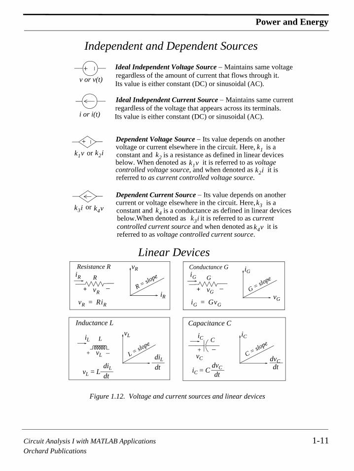
Linear devices are those in which there is a linear relationship between the voltage across that deviceand the current that flows through that device. Diodes and Transistors are non-linear devices, that is,their voltage-current relationship is non-linear. These will not be discussed in this text. A simple cir-cuit with a diode is presented in Chapter 3.
q t 0=15000 i td
0
15000
∫ 8e t 3600⁄– td0
28800
∫8
1– 3600⁄----------------------e t– 3600⁄
0
28800= = =
8– 3600× e 8– 1–( ) 28800 C or 28.8 kC≈=
imax 8 A (occurs at t=0)=
pmax vimax 12 8× 96 w= = =
W p td∫ vi td0
28800
∫ 12 8e t 3600⁄–×0
28800
∫ dt 961– 3600⁄
----------------------e t– 3600⁄0
28800= = = =
3.456 105× 1 e 8––( ) 345.6 KJ.≈=
Pave1T--- p td
0
T
∫1
28800--------------- 12 8e t 3600⁄–×
0
28800
∫ dt 345.6 103×
28.8 103×---------------------------- 12 w.= = = =
p 9 e0.16t2
1–( )= v 3 e0.4t 1+( )=
p vi, i pv---
9 e0.16t2
1–( )
3 e0.4t 1+( )------------------------------- 9 e0.4t 1+( ) e0.4t 1–( )
3 e0.4t 1+( )--------------------------------------------------- 3 e0.4t 1–( ) A= = = = =
q t0
t i tdt0
t
∫ 3 e0.4t 1–( ) td0
2
∫3
0.4-------e0.4t
0
23t 0
2– 7.5 e0.8 1–( ) 6– 3.19 C= = = = =
Circuit Analysis I with MATLAB Applications 1-11Orchard Publications
Power and Energy
Figure 1.12. Voltage and current sources and linear devices
+ − Ideal Independent Voltage Source − Maintains same voltage regardless of the amount of current that flows through it.
v or v(t)Its value is either constant (DC) or sinusoidal (AC).
Ideal Independent Current Source − Maintains same current regardless of the voltage that appears across its terminals.
i or i(t) Its value is either constant (DC) or sinusoidal (AC).
+ − Dependent Voltage Source − Its value depends on another voltage or current elsewhere in the circuit. Here, is a
or constant and is a resistance as defined in linear devices
Dependent Current Source − Its value depends on another current or voltage elsewhere in the circuit. Here, is aconstant and is a conductance as defined in linear devices
Linear Devices
R
CiC
Independent and Dependent Sources
+ −
vR
iR R = slo
pe G
+ −vG
Conductance G iG
vG G = slo
pe
Resistance R
iC = C
+ −
dvC dt
vC
vL
L = slo
pe
diL dt
Inductance L
LiL
vL = L
+ −
diL dt
vL
iC
C = slo
pe
dvC dt
Capacitance C
k1v k2i
k4vk3i
k1k2
k3k4
vR RiR=
vR
iR iG
iG GvG=
below. When denoted as it is referred to as voltage
below.
k2ik1v
controlled voltage source, and when denoted as it is referred to as current controlled voltage source.
When denoted as it is referred to as current
or
k3icontrolled current source and when denoted as it is k4vreferred to as voltage controlled current source.

Chapter 1 Basic Concepts and Definitions
1-12 Circuit Analysis I with MATLAB ApplicationsOrchard Publications
1.6 Active and Passive Devices
Independent and dependent voltage and current sources are active devices; they normally (but notalways) deliver power to some external device. Resistors, inductors and capacitors are passive devices;they normally receive (absorb) power from an active device.
1.7 Circuits and Networks
A network is the interconnection of two or more simple devices as shown in Figure 1.13.
Figure 1.13. A network but not a circuit
A circuit is a network which contains at least one closed path. Thus every circuit is a network but notall networks are circuits. An example is shown in Figure 1.14.
Figure 1.14. A network and a circuit
1.8 Active and Passive Networks
Active Network is a network which contains at least one active device (voltage or current source).
Passive Network is a network which does not contain any active device.
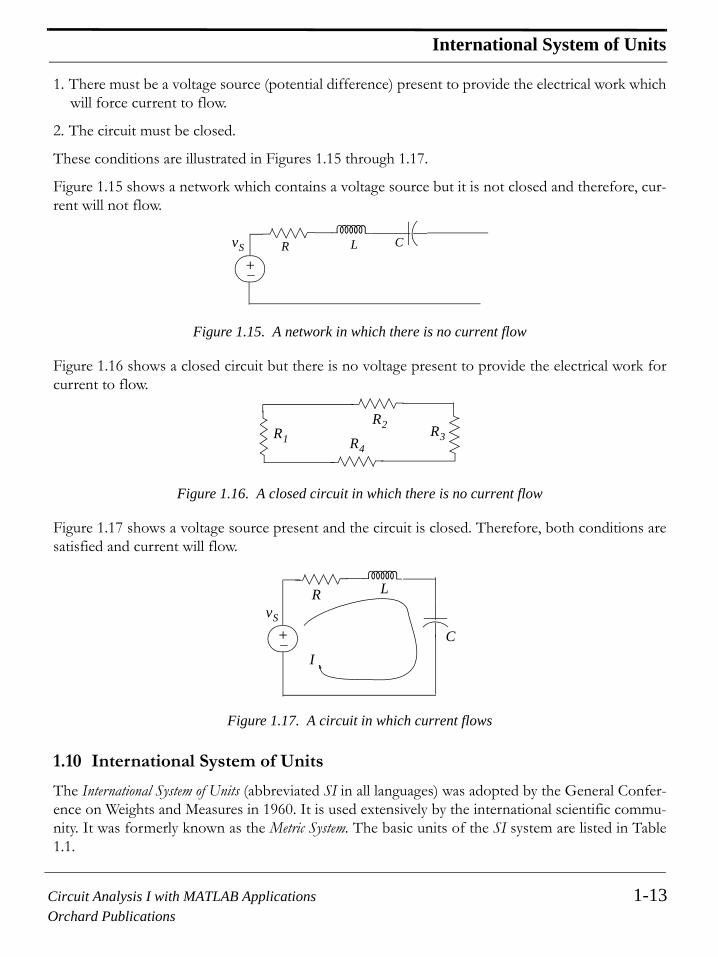
1.9 Necessary Conditions for Current Flow
There are two conditions which are necessary to set up and maintain a flow of current in a networkor circuit. These are:
+−
R L CvS
+−
L CvS
R1
R2
Circuit Analysis I with MATLAB Applications 1-13Orchard Publications
International System of Units
1. There must be a voltage source (potential difference) present to provide the electrical work whichwill force current to flow.
2. The circuit must be closed.
These conditions are illustrated in Figures 1.15 through 1.17.
Figure 1.15 shows a network which contains a voltage source but it is not closed and therefore, cur-rent will not flow.
Figure 1.15. A network in which there is no current flow
Figure 1.16 shows a closed circuit but there is no voltage present to provide the electrical work forcurrent to flow.
Figure 1.16. A closed circuit in which there is no current flow
Figure 1.17 shows a voltage source present and the circuit is closed. Therefore, both conditions aresatisfied and current will flow.
Figure 1.17. A circuit in which current flows
1.10 International System of Units
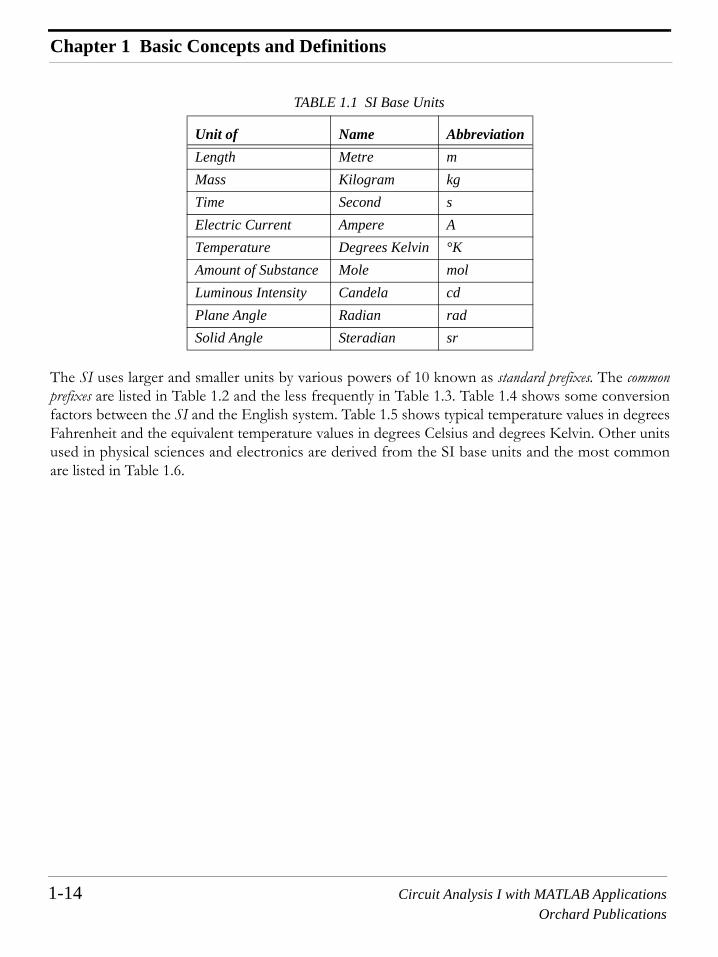
The International System of Units (abbreviated SI in all languages) was adopted by the General Confer-ence on Weights and Measures in 1960. It is used extensively by the international scientific commu-nity. It was formerly known as the Metric System. The basic units of the SI system are listed in Table1.1.
+−
R L CvS
R1
R2 R3R4
+−
R L
C
I
vS
Chapter 1 Basic Concepts and Definitions
1-14 Circuit Analysis I with MATLAB ApplicationsOrchard Publications
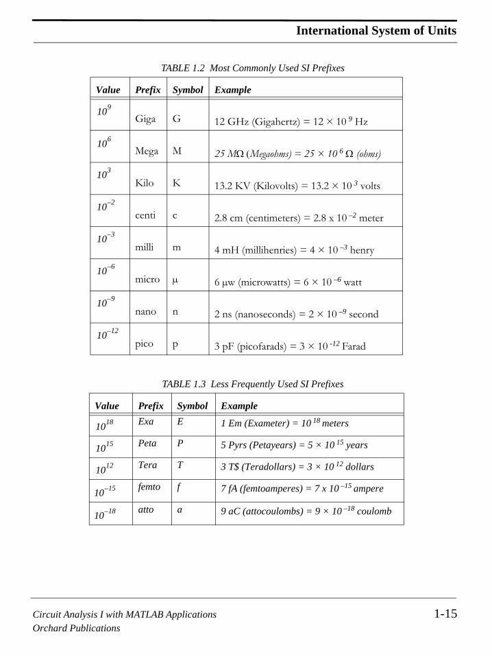
The SI uses larger and smaller units by various powers of 10 known as standard prefixes. The commonprefixes are listed in Table 1.2 and the less frequently in Table 1.3. Table 1.4 shows some conversionfactors between the SI and the English system. Table 1.5 shows typical temperature values in degreesFahrenheit and the equivalent temperature values in degrees Celsius and degrees Kelvin. Other unitsused in physical sciences and electronics are derived from the SI base units and the most commonare listed in Table 1.6.
TABLE 1.1 SI Base Units
Unit of Name Abbreviation
Length Metre m
Mass Kilogram kg
Time Second s
Electric Current Ampere A
Temperature Degrees Kelvin °K
Amount of Substance Mole mol
Luminous Intensity Candela cd
Plane Angle Radian rad
Solid Angle Steradian sr
Circuit Analysis I with MATLAB Applications 1-15Orchard Publications
International System of Units
TABLE 1.2 Most Commonly Used SI Prefixes
Value Prefix Symbol Example
Giga G 12 GHz (Gigahertz) = 12 × 10 9 Hz
Mega M 25 MΩ (Megaohms) = 25 × 10 6 Ω (ohms)
Kilo K 13.2 KV (Kilovolts) = 13.2 × 10 3 volts
centi c 2.8 cm (centimeters) = 2.8 x 10 –2 meter
milli m 4 mH (millihenries) = 4 × 10 –3 henry
micro µ 6 µw (microwatts) = 6 × 10 –6 watt
nano n 2 ns (nanoseconds) = 2 × 10 –9 second
pico p 3 pF (picofarads) = 3 × 10 -12 Farad
TABLE 1.3 Less Frequently Used SI Prefixes
Value Prefix Symbol Example
Exa E 1 Em (Exameter) = 10 18 meters
Peta P 5 Pyrs (Petayears) = 5 × 10 15 years
Tera T 3 T$ (Teradollars) = 3 × 10 12 dollars
femto f 7 fA (femtoamperes) = 7 x 10 –15 ampere
atto a 9 aC (attocoulombs) = 9 × 10 –18 coulomb
109
106
103
10 2–
10 3–
10 6–
10 9–
10 12–
1018
1015
1012
10 15–
10 18–

Chapter 1 Basic Concepts and Definitions
1-16 Circuit Analysis I with MATLAB ApplicationsOrchard Publications
TABLE 1.4 Conversion Factors
1 in. (inch) 2.54 cm (centimeters)
1 mi. (mile) 1.609 Km (Kilometers)
1 lb. (pound) 0.4536 Kg (Kilograms)
1 qt. (quart) 946 cm3 (cubic centimeters)
1 cm (centimeter) 0.3937 in. (inch)
1 Km (Kilometer) 0.6214 mi. (mile)
1 Kg (Kilogram) 2.2046 lbs (pounds)
1 lt. (liter) = 1000 cm3 1.057 quarts
1 Å (Angstrom) 10 –10 meter
1 mm (micron) 10 –6 meter
TABLE 1.5 Temperature Scale Equivalents
°F °C °K
–523.4 –273 0
32 0 273
0 –17.8 255.2
77 25 298
98.6 37 310
212 100 373

Circuit Analysis I with MATLAB Applications 1-17Orchard Publications
Sources of Energy
1.11 Sources of Energy
The principal sources of energy are from chemical processes (coal, fuel oil, natural gas, wood etc.)and from mechanical forms (water falls, wind, etc.). Other sources include nuclear and solar energy.
Example 1.6
A certain type of wood used in the generation of electric energy and we can get 12,000 BTUs froma pound (lb) of that wood when burned. Suppose that a computer system that includes a monitor, aprinter, and other peripherals absorbs an average power of 500 w gets its energy from that burned
TABLE 1.6 SI Derived Units
Unit of Name Formula
Force Newton
Pressure or Stress Pascal
Work or Energy Joule
Power Watt
Voltage Volt
Resistance Ohm
Conductance Siemens or
Capacitance Farad
Inductance Henry
Frequency Hertz
Quantity of Electricity Coulomb
Magnetic Flux Weber
Magnetic Flux Density Tesla
Luminous Flux Lumen
Illuminance Lux
Radioactivity Becquerel
Radiation Dose Gray
Volume Litre
N( ) N kg m⋅ s2⁄=
Pa( ) Pa N m2⁄=
J( ) J N m⋅=
W( ) W J s⁄=
V( ) V W A⁄=
Ω( ) Ω V A⁄=
S( ) Ω 1–( ) S A V⁄=
F( ) F A s⋅ V⁄=
H( ) H V s⋅ A⁄=
Hz( ) Hz 1 s⁄=
C( ) C A s⋅=
Wb( ) Wb V s⋅=
T( ) T Wb m2⁄=
lm( ) lm cd sr⋅=
lx( ) lx lm m2⁄=
Bq( ) Bq s 1–=
Gy( ) S J kg⁄=
L( ) L m3 10 3–×=

Chapter 1 Basic Concepts and Definitions
1-18 Circuit Analysis I with MATLAB ApplicationsOrchard Publications
wood and it is turned on for 8 hours. It is known that 1 BTU is equivalent to 778.3 ft-lb of energy,and 1 joule is equivalent to 0.7376 ft-lb.
Compute:
a. the energy consumption during this 8-hour interval
b. the cost for this energy consumption if the rate is $0.15 per kw-hr
c. the amount of wood in lbs burned during this time interval.
Solution:
a. Energy consumption for 8 hours is
b. Since ,
c. Wood burned in 8 hours,
1.12 Summary
• Two identically charged (both positive or both negative) particles possess a charge of one coulombwhen being separated by one meter in a vacuum, repel each other with a force of newton
where . Thus, the force with which two electrically chargedbodies attract or repel one another depends on the product of the charges (in coulombs) in bothobjects, and also on the distance between the objects. If the polarities are the same (negative/negative or positive/positive), the so-called coulumb force is repulsive; if the polarities areopposite (negative/positive or positive/negative), the force is attractive. For any two chargedbodies, the coulomb force decreases in proportion to the square of the distance between theircharge centers.
• Electric current is defined as the instantaneous rate at which net positive charge is moving pastthis point in that specified direction, that is,
Energy W Pavet 500 w 8 hrs × 3600 s1 hr
----------------× 14.4 Mjoules= = =
1 kilowatt hour– 3.6 106 joules×=
Cost $0.15kw hr–------------------ 1 kw hr–
3.6 106 joules×----------------------------------------× 14.4 106×× $0.60= =
14.4 106 joules× 0.7376 f t lb–joule---------------- 1 BTU
778.3 f t lb–-------------------------------× 1 lb
12000 BTU----------------------------×× 1.137 lb=
10 7– c2
c velocity of light 3 108 m s⁄×≈=
i dqdt------ q∆
t∆------
t∆ 0→lim= =

Circuit Analysis I with MATLAB Applications 1-19Orchard Publications
Summary
• The unit of current is the ampere, abbreviated as A, and corresponds to charge q moving at therate of one coulomb per second.
• In a two-terminal device the current entering one terminal is the same as the current leaving theother terminal.
• The voltage (potential difference) across a two-terminal device is defined as the work required tomove a positive charge of one coulomb from one terminal of the device to the other terminal.
• The unit of voltage is the volt (abbreviated as V or v) and it is defined as
• Power p is the rate at which energy (or work) W is expended. That is,
• Absorbed power is proportional both to the current and the voltage needed to transfer one cou-lomb through the device. The unit of power is the watt and
• The passive sign convention states that if the arrow representing the current i and the plus (+)minus (−) pair are placed at the device terminals in such a way that the current enters the deviceterminal marked with the plus (+) sign, and if both the arrow and the sign pair are labeled withthe appropriate algebraic quantities, the power absorbed or delivered to the device can beexpressed as . If the numerical value of this product is positive, we say that the device isabsorbing power which is equivalent to saying that power is delivered to the device. If, on theother hand, the numerical value of the product is negative, we say that the device deliverspower to some other device.
• An ideal independent voltage source maintains the same voltage regardless of the amount of cur-rent that flows through it.
• An ideal independent current source maintains the same current regardless of the amount of volt-age that appears across its terminals.
• The value of an dependent voltage source depends on another voltage or current elsewhere in thecircuit.
• The value of an dependent current source depends on another current or voltage elsewhere inthe circuit.
• Ideal voltage and current sources are just mathematical models. We will discuss practical voltageand current sources in Chapter 3.
1 volt 1 joule1 coulomb-----------------------------=
Power p dWdt
--------= =
1 watt 1 volt 1 ampere×=
p vi=
p vi=

Chapter 1 Basic Concepts and Definitions
1-20 Circuit Analysis I with MATLAB ApplicationsOrchard Publications
• Independent and Dependent voltage and current sources are active devices; they normally (butnot always) deliver power to some external device.
• Resistors, inductors, and capacitors are passive devices; they normally receive (absorb) powerfrom an active device.
• A network is the interconnection of two or more simple devices.
• A circuit is a network which contains at least one closed path. Thus every circuit is a network butnot all networks are circuits.
• An active network is a network which contains at least one active device (voltage or currentsource).
• A passive network is a network which does not contain any active device.
• To set up and maintain a flow of current in a network or circuit there must be a voltage source(potential difference) present to provide the electrical work which will force current to flow andthe circuit must be closed.
• Linear devices are those in which there is a linear relationship between the voltage across thatdevice and the current that flows through that device.
• The International System of Units is used extensively by the international scientific community. Itwas formerly known as the Metric System.
• The principal sources of energy are from chemical processes (coal, fuel oil, natural gas, wood etc.)and from mechanical forms (water falls, wind, etc.). Other sources include nuclear and solarenergy.

Circuit Analysis I with MATLAB Applications 1-21Orchard Publications
Exercises
1.13 Exercises
Multiple choice
1. The unit of charge is the
A. ampere
B. volt
C. watt
D. coulomb
E. none of the above
2. The unit of current is the
A. ampere
B. coulomb
C. watt
D. joule
E. none of the above
3. The unit of electric power is the
A. ampere
B. coulomb
C. watt
D. joule
E. none of the above
4. The unit of energy is the
A. ampere
B. volt
C. watt
D. joule
E. none of the above
5. Power is
A. the integral of energy

Chapter 1 Basic Concepts and Definitions
1-22 Circuit Analysis I with MATLAB ApplicationsOrchard Publications
B. the derivative of energy
C. current times some constant
D. voltage times some constant
E. none of the above
6. Active voltage and current sources
A. always deliver power to other external devices
B. normally deliver power to other external devices
C. neither deliver or absorb power to or from other devices
D. are just mathematical models
E. none of the above
7. An ideal independent voltage source
A. maintains the same voltage regardless of the amount of current that flows through it
B. maintains the same current regardless of the voltage rating of that voltage source
C. always delivers the same amount of power to other devices
D. is a source where both voltage and current can be variable
E. none of the above
8. An ideal independent current source
A. maintains the same voltage regardless of the amount of current that flows through it
B. maintains the same current regardless of the voltage that appears across its terminals
C. always delivers the same amount of power to other devices
D. is a source where both voltage and current can be variable
E. none of the above
9. The value of a dependent voltage source can be denoted as
A. where k is a conductance value
B. where k is a resistance value
C. where k is an inductance value
D. where k is a capacitance value
k
k
kV
kI
kV
kI

Circuit Analysis I with MATLAB Applications 1-23Orchard Publications
Exercises
E. none of the above
10. The value of a dependent current source can be denoted as
A. where k is a conductance value
B. where k is a resistance value
C. where k is an inductance value
D. where k is a capacitance value
E. none of the above
Problems
1. A two terminal device consumes energy as shown by the waveform of Figure 1.18 below, and thecurrent through this device is . Find the voltage across this device at t =0.5, 1.5, 4.75 and 6.5 ms. Answers:
Figure 1.18. Waveform for Problem 1
2. A household light bulb is rated 75 watts at 120 volts. Compute the number of electrons per sec-ond that flow through this bulb when it is connected to a 120 volt source.Answer:
3. An airplane, whose total mass is 50,000 metric tons, reaches a height of 32,808 feet in 20 minutesafter takeoff.
a. Compute the potential energy that the airplane has gained at this height. Answer:
b. If this energy could be converted to electric energy with a conversion loss of 10%, how muchwould this energy be worth at $0.15 per kilowatt-hour? Answer:
c. If this energy were converted into electric energy during the period of 20 minutes, what aver-age number of kilowatts would be generated? Answer:
kV
kI
kV
kI
i t( ) 2 4000πt Acos=
2.5 V 0 V 2.5 V 2.5 V–,,,
1 t (ms)
W (mJ)
0
10
2 753 4 6
5
3.9 1018 electrons s⁄×
1 736 MJ,
$65.10
1 450 Kw,

Chapter 1 Basic Concepts and Definitions
1-24 Circuit Analysis I with MATLAB ApplicationsOrchard Publications
4. The power input to a television station transmitter is 125 kw and the output is 100 kw which istransmitted as radio frequency power. The remaining 25 kw of power is converted into heat.a. How many BTUs per hour does this transmitter release as heat?
Answer:
b. How many electron-volts per second is this heat equivalent to?
Answer:
1 BTU 1054.8 J=
85 234 BTU hr⁄,
1 electron volt– 1.6 10 19– J×= 1.56 10 23× electron volts– sec.
------------------------------------------

Circuit Analysis I with MATLAB Applications 1-25Orchard Publications
Answers to Exercises
1.14 Answers to Exercises
Dear Reader:
The remaining pages on this chapter contain answers to the multiple-choice questions and solutionsto the exercises.
You must, for your benefit, make an honest effort to answer the multiple-choice questions and solvethe problems without first looking at the solutions that follow. It is recommended that first you gothrough and answer those you feel that you know. For the multiple-choice questions and problemsthat you are uncertain, review this chapter and try again. If your answers to the problems do notagree with those provided, look over your procedures for inconsistencies and computational errors.Refer to the solutions as a last resort and rework those problems at a later date.
You should follow this practice with the multiple-choice and problems on all chapters of this book.

Chapter 1 Basic Concepts and Definitions
1-26 Circuit Analysis I with MATLAB ApplicationsOrchard Publications
Multiple choice
1. D
2. A
3. C
4. D
5. B
6. B
7. A
8. B
9. B
10. A
Problems
1.
a.
b.
c.
d.
v pi--- dW dt⁄
i----------------- slope
i--------------= = =
slope 01 ms 5 mJ
1 ms------------ 5 J s⁄= =
v t 0.5 ms=5 J s⁄
2 4000π 0.5 10 3–×( ) Acos--------------------------------------------------------------- 5 J s⁄
2 2π Acos------------------------ 5 J s⁄
2 A-------------- 2.5 V= = = =
slope 12 ms 0=
v t 1.5 ms=0i--- 0 V= =
slope 45 ms 5– mJ
1 ms--------------- 5– J s⁄= =
v t 4.75 ms=5– J s⁄
2 4000π 4.75 10 3–×( ) Acos------------------------------------------------------------------ 5– J s⁄
2 19π Acos--------------------------- 5– J s⁄
2 π Acos--------------------- 5– J s⁄
2 A–----------------- 2.5 V= = = = =

Circuit Analysis I with MATLAB Applications 1-27Orchard Publications
Answers to Exercises
2.
3.
where and
Then,
a.
slope 67 ms 5– mJ
1 ms--------------- 5– J s⁄= =
v t 6.5 ms=5– J s⁄
2 4000π 6.5 10 3–×( ) Acos--------------------------------------------------------------- 5– J s⁄
2 26π Acos--------------------------- 5– J s⁄
2 A----------------- 2.5– V= = = =
i pv--- 75 w
120 V-------------- 5
8--- A= = =
q i tdt0
t
∫=
q t 1 s=58--- td
0
1 s
∫58---t
0
1 s 58--- C s⁄= = =
58--- C s⁄ 6.24 1018 electrons×
1 C------------------------------------------------------× 3.9 1018 electrons s⁄×=
Wp Wk12---mv2= =
m mass in kg= v velocity in meters sec.⁄=
33 808 ft 0.3048 mft
-----------------------×, 10 000 m, 10 Km= =
20 minutes 60 sec.min
-----------------× 1 200 sec.,=
v 10 000 m,1 200 sec.,-------------------------- 25
3------ m s⁄= =
50 000 metric tons 1 000 Kg,metric ton---------------------------×, 5 107× Kg=
Wp Wk12--- 5 107×( ) 25
3------⎝ ⎠
⎛ ⎞ 2173.61 107× J 1 736 MJ,≈= = =

Chapter 1 Basic Concepts and Definitions
1-28 Circuit Analysis I with MATLAB ApplicationsOrchard Publications
b.
and with 10% conversion loss, the useful energy is
c.
4.
a.
b.
1 joule 1 watt-sec=
1 736 106J 1 watt-sec1 joule
--------------------------××, 1 Kw1 000 w,---------------------× 1 hr
3 600 sec.,--------------------------× 482.22 Kw-hr=
482.22 0.9× 482.22 0.9 434 Kw-hr=×=
Cost of Energy $0.15Kw-hr---------------- 434 Kw-hr× $65.10= =
PaveWt
----- 1 736 MJ,
20 min 60 secmin
---------------×---------------------------------------- 1.45 Mw 1450 Kw= = = =
1 BTU 1054.8 J=
25 000 watts 1 joule sec.⁄watt
-------------------------------×, 1 BTU1054.8 J--------------------- 3600 sec.
1 hr-----------------------×× 85 234 BTU hr⁄,=
1 electron volt– 1.6 10 19– J×=
1 electron volt– sec.
------------------------------------------- 1.6 10 19– J× sec.
------------------------------- 1.6 10 19– watt×= =
25 000 watts 1 electron volt– sec.⁄
1.6 10 19– watt×----------------------------------------------------------×, 1.56 10 23× electron volts–
sec.------------------------------------------=

Circuit Analysis I with MATLAB Applications 2-1Orchard Publications
Chapter 2
Analysis of Simple Circuits
his chapter defines constant and instantaneous values, Ohm’s law, and Kirchhoff ’s Currentand Voltage laws. Series and parallel circuits are also defined and nodal, mesh, and loop analy-ses are introduced. Combinations of voltage and current sources and resistance combinations
are discussed, and the voltage and current division formulas are derived.
2.1 Conventions
We will use lower case letters such as , , and to denote instantaneous values of voltage, current,and power respectively, and we will use subscripts to denote specific voltages, currents, resistances,etc. For example, and will be used to denote voltage and current sources respectively. Nota-tions like and will be used to denote the voltage across resistance and the currentthrough resistance respectively. Other notations like or will represent the voltage (poten-tial difference) between point or point with respect to some arbitrarily chosen reference pointtaken as “zero” volts or “ground”.
The designations or will be used to denote the voltage between point or point withrespect to point or respectively. We will denote voltages as and whenever we wish toemphasize that these quantities are time dependent. Thus, sinusoidal (AC) voltages and currents willbe denoted as and respectively. Phasor quantities, to be inroduced in Chapter 6, will be rep-resented with bold capital letters, for phasor voltage and for phasor current.
2.2 Ohm’s Law
We recall from Chapter 1 that resistance is a constant that relates the voltage and the current as:
(2.1)
This relation is known as Ohm’s law.
The unit of resistance is the Ohm and its symbol is the Greek capital letter . One ohm is the resis-tance of a conductor such that a constant current of one ampere through it produces a voltage ofone volt between its ends. Thus,
(2.2)
T
v i p
vS iS
vR1 iR2 R1
R2 vA v1
A 1
vAB v12 A 1
B 2 v t( ) i t( )
v t( ) i t( )V I
R
vR RiR=
Ω
1 Ω 1 V1 A--------=

Chapter 2 Analysis of Simple Circuits
2-2 Circuit Analysis I with MATLAB ApplicationsOrchard Publications
Physically, a resistor is a device that opposes current flow. Resistors are used as a current limiting devicesand as voltage dividers.
In the previous chapter we defined conductance as the constant that relates the current and the volt-age as
(2.3)
This is another form of Ohm’s law since by letting and , we get
(2.4)
The unit of conductance is the siemens or mho (ohm spelled backwards) and its symbol is or Thus,
(2.5)
Resistances (or conductances) are commonly used to define an “open circuit” or a “short circuit”.An open circuit is an adjective describing the “open space” between a pair of terminals, and can bethought of as an “infinite resistance” or “zero conductance”. In contrast, a short circuit is an adjectivedescribing the connection of a pair of terminals by a piece of wire of “infinite conductance” or apiece of wire of “zero” resistance.
The current through an “open circuit” is always zero but the voltage across the open circuit terminalsmay or may not be zero. Likewise, the voltage across a short circuit terminals is always zero but thecurrent through it may or may not be zero. The open and short circuit concepts and their equivalentresistances or conductances are shown in Figure 2.1.
Figure 2.1. The concepts of open and short circuits
The fact that current does not flow through an open circuit and that zero voltage exists across theterminals of a short circuit, can also be observed from the expressions and .
That is, since , infinite means zero and zero means infinite . Then, for a finite volt-
age, say , and an open circuit,
G
iG GvG=
iG iR= vG vR=
G 1R---=
S Ω 1–
1 Ω 1– 1 A1 V--------=
A +
−
OpenCircuit
i = 0B
i = 0
R = ∞G = 0
A+
−B
A +
−
ShortCircuit
B
iR = 0G = ∞
A +
−B
ivAB 0= vAB 0=
vR RiR= iG GvG=
G 1R---= R G R G
vG

Circuit Analysis I with MATLAB Applications 2-3Orchard Publications
Power Absorbed by a Resistor
(2.6)
Likewise, for a finite current, say iR, and a short circuit,
(2.7)
Reminder:
We must remember that the expressions
and
are true only when the passive sign convention is observed. This is consistent with our classificationof and being passive devices and thus implies the current direction and voltagepolarity are as shown in Figure 2.2.
Figure 2.2. Voltage polarity and current direction in accordance to passive sign convention
But if the voltage polarities and current directions are as shown in Figure 2.3, then,
(2.8)
Figure 2.3. Voltage polarity and current direction not in accordance to passive sign convention
Note: “Negative resistance,” as shown in (2.8), can be thought of as being a math model that sup-plies energy.
2.3 Power Absorbed by a Resistor
A resistor, being a passive device, absorbs power. This absorbed power can be found from Ohm’slaw, that is,
and the power relation
iGG 0→lim GvGG 0→
lim 0= =
vRR 0→lim RiRR 0→
lim 0= =
vR RiR=
iG GvG=
R G vR RiR=
+ −
R
+−
R IRIR
vRvR
vR R– iR=
+−R
+ −R
IRIR
vR vR
vR RiR=

Chapter 2 Analysis of Simple Circuits
2-4 Circuit Analysis I with MATLAB ApplicationsOrchard Publications
Then,
(2.9)
The voltage, current, resistance and power relations are arranged in the pie chart shown in Figure 2.4.
Figure 2.4. Pie chart for showing relations among voltage, current, resistance, and power
Note: A resistor, besides its resistance rating (ohms) has a power rating in watts commonly referred to asthe wattage of the resistor. Common resistor wattage values are ¼ watt, ½ watt, 1 watt, 2 watts, 5 wattsand so on. This topic will be discussed in Section 2.16.
2.4 Energy Dissipated in a Resistor
A resistor, by its own nature, dissipates energy in the form of heat; it never stores energy. The energydissipated in a resistor during a time interval, say from to , is given by the integral of the instan-taneous power .Thus,
(2.10)
pR vR iR=
pR vR iR RiR( ) iR RiR2 vR
vRR-----⎝ ⎠
⎛ ⎞ vR2
R-----= = = = =
P I
RVPR
PI IR
VI
I 2 R
V 2
RVR P
V
P R⁄
PI 2
V 2
P
VI
POWER (W
atts)
VOLTAGE (Volts)
CURRENT (Amperes)
RESIST
ANCE (Ohm
s)
t1 t2
pR
WR diss pR tdt1
t2
∫=

Circuit Analysis I with MATLAB Applications 2-5Orchard Publications
Nodes, Branches, Loops and Meshes
If the power is constant, say , then (2.10) reduces to
(2.11)
Alternately, if the energy is known, we can find the power by taking the derivative of the energy, thatis,
(2.12)
Reminder: When using all formulas, we must express the quantities involved in their primary units. Forinstance in (2.11) above, the energy is in joules when the power is in watts and the time is in seconds.
2.5 Nodes, Branches, Loops and Meshes
Definition 2.1
A node is the common point at which two or more devices (passive or active) are connected. Anexample of a node is shown in Figure 2.5.
Figure 2.5. Definition of node
Definition 2.2
A branch is a simple path composed of one single device as shown in Figure 2.6.
Figure 2.6. Definition of branch
Definition 2.3
A loop is a closed path formed by the interconnection of simple devices. For example, the networkshown in Figure 2.7 is a loop.
P
WR diss Pt=
pR tdd WR diss=
+−
Node
+ −
Node Branch
R C vS

Chapter 2 Analysis of Simple Circuits
2-6 Circuit Analysis I with MATLAB ApplicationsOrchard Publications
Figure 2.7. Definition of a loop
Definition 2.4
A mesh is a loop which does not enclose any other loops. For example, in the circuit shown in Figure2.8, is both a loop and a mesh, but is a loop but not a mesh.
Figure 2.8. Example showing the difference between mesh and loop
2.6 Kirchhoff ’s Current Law (KCL)
KCL states that the algebraic sum of all currents leaving (or entering) a node is equal to zero. For example,in Figure 2.9, if we assign a plus (+) sign to the currents leaving the node, we must assign a minus (−)sign to the currents entering the node. Then by KCL,
(2.13)
Figure 2.9. Node to illustrate KCL
But if we assign a plus (+) sign to the currents entering the node and minus (−) sign to the currentsleaving the node, then by KCL,
(2.14)
+−L
C
RvS
ABEF ABCDEF
+−
A B C
DEF
vS
R1
R2
L C
i1– i2– i3 i4+ + 0=
i4
i1 i2
i3
i1 i2 i3– i4–+ 0=

Circuit Analysis I with MATLAB Applications 2-7Orchard Publications
Kirchhoff’s Voltage Law (KVL)
or
(2.15)
We observe that (2.13) and (2.15) are the same; therefore, it does not matter which we choose asplus (+).
Convention: In our subsequent discussion we will assign plus (+) signs to the currents leaving the node.
2.7 Kirchhoff ’s Voltage Law (KVL)
KVL states that the algebraic sum of the voltage drops (voltages from + to −) or voltage rises (voltages from− to +) around any closed path (mesh or loop) in a circuit is equal to zero. For example, in the circuitshown in Figure 2.10, voltages , , , and represent the voltages across devices 1, 2, 3, and 4respectively, and have the polarities shown.
Figure 2.10. Circuit to illustrate KVL
Now, if we assign a (+) sign to the voltage drops, we must assign a (−) sign to the voltage rises. Then,by KVL starting at node and going clockwise we get:
(2.16)
or going counterclockwise, we get:
(2.17)
Alternately, if we assign a (+) sign to the voltage rises, we must assign a (−) sign to the voltage drops.Then, by KVL starting again at node A and going clockwise we get:
(2.18)
or going counterclockwise, we get:
(2.19)
We observe that expressions (2.16) through (2.19) are the same.
i1– i2– i3 i4+ + 0=
v1 v2 v3 v4
Device 1
Device 2
Device 4
Device 3−
− ++
−
+
− +A
v1
v2v3
v4
A
v1– v2– v3 v4+ + 0=
v4– v3– v2 v1+ + 0=
v1 v2 v3– v4–+ 0=
v4 v3 v2– v1–+ 0=

Chapter 2 Analysis of Simple Circuits
2-8 Circuit Analysis I with MATLAB ApplicationsOrchard Publications
Convention: In our subsequent discussion we will assign plus (+) signs to voltage drops.
Definition 2.5
Two or more devices are said to be connected in series if and only if the same current flows throughthem. For example, in the circuit of Figure 2.11, the same current flows through the voltage source,the resistance, the inductance and the capacitance. Accordingly, this is classified as a series circuit.
Figure 2.11. A simple series circuit
Definition 2.6
Two or more devices are said to be connected in parallel if and only if the same voltage exists across eachof the devices. For example, in the circuit of Figure 2.12, the same voltage exists across the cur-rent source, the conductance, the inductance, and the capacitance and therefore it is classified as aparallel circuit
Figure 2.12. A simple parallel circuit
Convention: In our subsequent discussion we will adopt the conventional current flow, i.e., the current that flowsfrom a higher (+) to a lower (−) potential. For example, if in Figure 2.13 we are given the indicatedpolarity,
Figure 2.13. Device with established voltage polarity
i
+−L
C
RvS
vAB
L
C
G L CG
A
B
A A A A
B B B B
iSiS
+ −
R
vR

Circuit Analysis I with MATLAB Applications 2-9Orchard Publications
Kirchhoff’s Voltage Law (KVL)
then, the current arrow will be pointing to the right direction as shown in Figure 2.14.
Figure 2.14. Direction of conventional current flow in device with established voltage polarity
Alternately, if current flows in an assumed specific direction through a device thus producing a volt-age, we will assign a (+) sign at the terminal of the device at which the current enters. For example,if we are given this designation a device in which the current direction has been established asshown in Figure 2.15,
Figure 2.15. Device with established conventional current direction
then we assign (+) and (−) as shown in Figure 2.16.
Figure 2.16. Voltage polarity in a device with established conventional current flow
Note: Active devices, such as voltage and current sources, have their voltage polarity and currentdirection respectively, established as part of their notation. The current through and the volt-age across these devices can easily be determined if these devices deliver power to the rest of the cir-cuit. Thus with the voltage polarity as given in the circuit of Figure 2.17 (a), we assign a clock-wise direction to the current as shown in Figure 2.17 (b). This is consistent with the passivesign convention since we have assumed that the voltage source delivers power to the rest ofthe circuit.
Figure 2.17. Direction of conventional current flow produced by voltage sources
+ −
R
vR
R
+ −
RiR
vR
−Rest of the
Circuit+
i
(b)
−Rest of the
Circuit+
(a)
vSvS
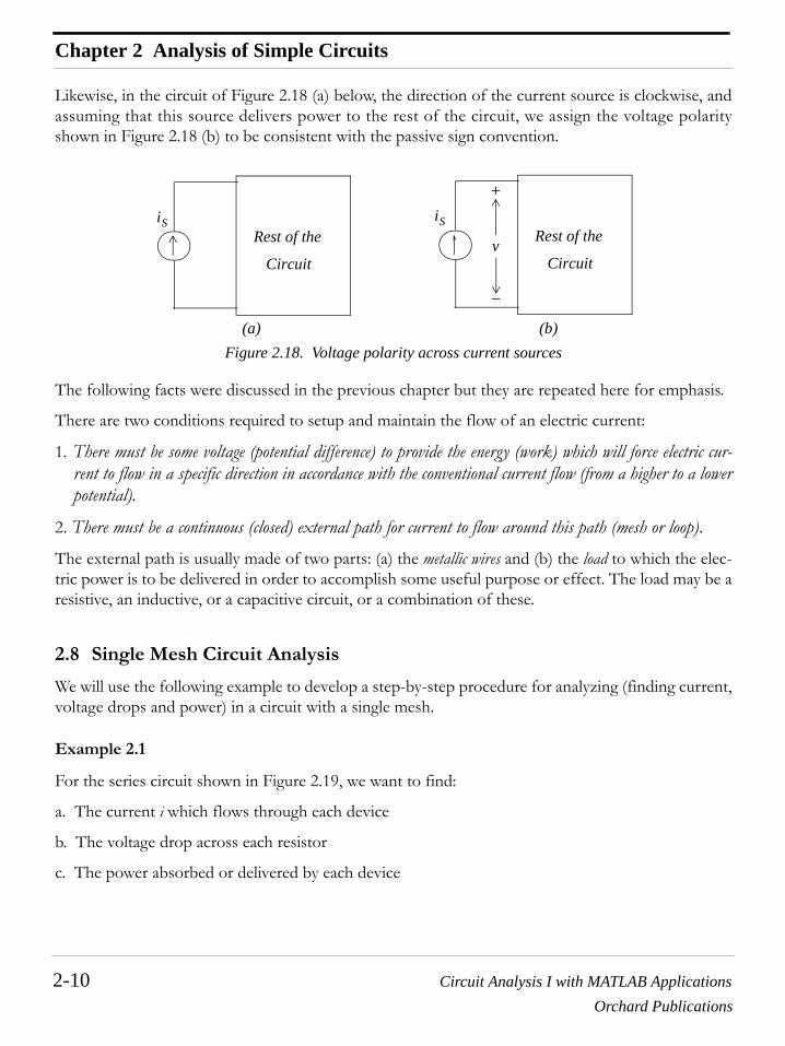
Chapter 2 Analysis of Simple Circuits
2-10 Circuit Analysis I with MATLAB ApplicationsOrchard Publications
Likewise, in the circuit of Figure 2.18 (a) below, the direction of the current source is clockwise, andassuming that this source delivers power to the rest of the circuit, we assign the voltage polarityshown in Figure 2.18 (b) to be consistent with the passive sign convention.
Figure 2.18. Voltage polarity across current sources
The following facts were discussed in the previous chapter but they are repeated here for emphasis.
There are two conditions required to setup and maintain the flow of an electric current:
1. There must be some voltage (potential difference) to provide the energy (work) which will force electric cur-rent to flow in a specific direction in accordance with the conventional current flow (from a higher to a lowerpotential).
2. There must be a continuous (closed) external path for current to flow around this path (mesh or loop).
The external path is usually made of two parts: (a) the metallic wires and (b) the load to which the elec-tric power is to be delivered in order to accomplish some useful purpose or effect. The load may be aresistive, an inductive, or a capacitive circuit, or a combination of these.
2.8 Single Mesh Circuit Analysis
We will use the following example to develop a step-by-step procedure for analyzing (finding current,voltage drops and power) in a circuit with a single mesh.
Example 2.1
For the series circuit shown in Figure 2.19, we want to find:
a. The current i which flows through each device
b. The voltage drop across each resistor
c. The power absorbed or delivered by each device
Rest of the
Circuit
Rest of the
Circuit
+
−
v
(a) (b)
iS iS
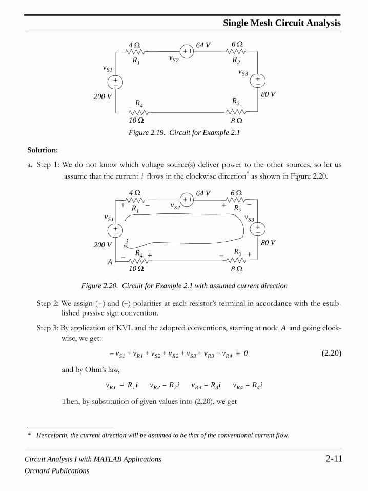
Circuit Analysis I with MATLAB Applications 2-11Orchard Publications
Single Mesh Circuit Analysis
Figure 2.19. Circuit for Example 2.1
Solution:
a. Step 1: We do not know which voltage source(s) deliver power to the other sources, so let usassume that the current flows in the clockwise direction* as shown in Figure 2.20.
Figure 2.20. Circuit for Example 2.1 with assumed current direction
Step 2: We assign (+) and (−) polarities at each resistor’s terminal in accordance with the estab-lished passive sign convention.
Step 3: By application of KVL and the adopted conventions, starting at node and going clock-wise, we get:
(2.20)
and by Ohm’s law,
Then, by substitution of given values into (2.20), we get
* Henceforth, the current direction will be assumed to be that of the conventional current flow.
+−
+ −
+−
200 V 80 V
64 V
10 Ω 8 Ω
R1
4 Ω 6 Ω
R2
R3R4
vS3vS1
vS2
i
+−
+ −
+−
200 V 80 V
64 V4 Ω 6 Ω
10 Ω 8 Ω
i
+ − + −
+−+−A
R1 R2
R3R4
vS1
vS2
vS3
A
vS1– vR1 vS2+ + vR2 vS3 vR3 vR4+ + + + 0=
vR1 R1i vR2 R2i vR3 R3i vR4 R4i====
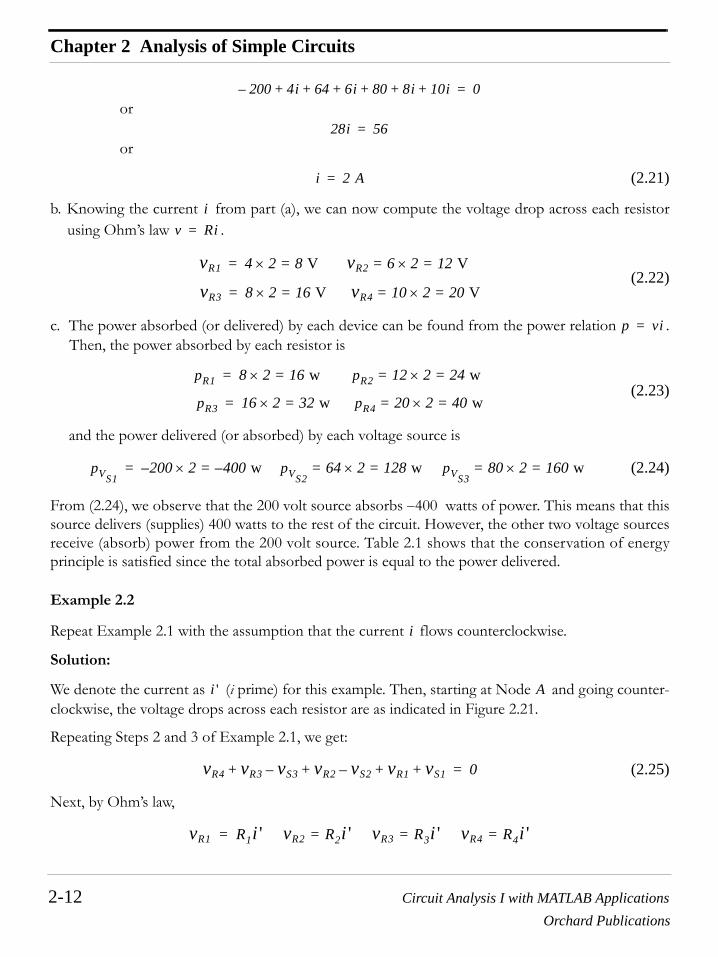
Chapter 2 Analysis of Simple Circuits
2-12 Circuit Analysis I with MATLAB ApplicationsOrchard Publications
or
or
(2.21)
b. Knowing the current from part (a), we can now compute the voltage drop across each resistorusing Ohm’s law .
(2.22)
c. The power absorbed (or delivered) by each device can be found from the power relation .Then, the power absorbed by each resistor is
(2.23)
and the power delivered (or absorbed) by each voltage source is
(2.24)
From (2.24), we observe that the 200 volt source absorbs −400 watts of power. This means that thissource delivers (supplies) 400 watts to the rest of the circuit. However, the other two voltage sourcesreceive (absorb) power from the 200 volt source. Table 2.1 shows that the conservation of energyprinciple is satisfied since the total absorbed power is equal to the power delivered.
Example 2.2
Repeat Example 2.1 with the assumption that the current flows counterclockwise.
Solution:
We denote the current as (i prime) for this example. Then, starting at Node and going counter-clockwise, the voltage drops across each resistor are as indicated in Figure 2.21.
Repeating Steps 2 and 3 of Example 2.1, we get:
(2.25)
Next, by Ohm’s law,
200– 4i 64+ + 6i 80 8i 10i+ + + + 0=
28i 56=
i 2 A=
iv Ri=
vR1 4 2× 8 V= vR2 6 2× 12 V= ==
vR3 8 2× 16 V= vR4 10 2× 20 V= ==
p vi=
pR1 8 2× 16 w= pR2 12 2× 24 w= ==
pR3 16 2× 32 w= pR4 20 2× 40 w= ==
pVS1200– 2× 400– w = pVS2
64 2× 128 w = pVS380 2× 160 w== ==
i
i ' A
vR4 vR3 vS3–+ vR2 vS2– vR1 vS1+ + + 0=
vR1 R1i ' vR2 R2i ' vR3 R3i ' vR4 R4i '====

Circuit Analysis I with MATLAB Applications 2-13Orchard Publications
Single Mesh Circuit Analysis
Figure 2.21. Circuit for Example 2.2
By substitution of given values, we get
or
or
(2.26)
Comparing (2.21) with (2.26) we see that as expected.
TABLE 2.1 Power delivered or absorbed by each device on the circuit of Figure 2.19
Device Power Delivered (watts) Power Absorbed (watts)
200 V Source 400
64 V Source 128
80 V Source 160
4 Ω Resistor 16
6 Ω Resistor 24
8 Ω Resistor 32
10 Ω Resistor 40
Total 400 400
+−
+ −
+−
200 V 80 V
64 V4 Ω 6 Ω
10 Ω 8 Ω
+− +−
+ −+ −A
R1 R2
R3R4
i '
vS2
vS1 vS3
200 4i ' 64–+ 6i ' 80– 8i ' 10i '+ + + 0=
28i ' 56–=
i ' 2– A=
i ' i–=

Chapter 2 Analysis of Simple Circuits
2-14 Circuit Analysis I with MATLAB ApplicationsOrchard Publications
Definition 2.7
A single node-pair circuit is one in which any number of simple elements are connected between thesame pair of nodes. For example, the circuit of Figure 2.22 (a), which is more conveniently shown asFigure 2.22 (b), is a single node-pair circuit.
Figure 2.22. Circuit with a single node-pair
2.9 Single Node-Pair Circuit Analysis
We will use the following example to develop a step-by-step procedure for analyzing (finding cur-rents, voltage drop and power) in a circuit with a single node-pair.
Example 2.3
For the parallel circuit shown in Figure 2.23, find:
a. The voltage drop across each device
b. The current i which flows through each conductance
c. The power absorbed or delivered by each device
Figure 2.23. Circuit for Example 2.3
iS
L
C
G
iS
L CG
A
B
A A A A
B B B B (a) (b)
12 A 24 A18 A
I1 I2 I3G2G1 G3
4 Ω 1– 6 Ω 1– 8 Ω 1–

Circuit Analysis I with MATLAB Applications 2-15Orchard Publications
Single Node-Pair Circuit Analysis
Solution:
a. Step 1: We denote the single node-pair with the letters and as shown in Figure 2.24. It isimportant to observe that the same voltage (or potential difference) exists across eachdevice. Node is chosen as our reference node and it is convenient to assume that this
reference node is at zero potential (ground) as indicated by the symbol
Figure 2.24. Circuit for Example 2.3 with assumed current directions
Step 2: We assign currents through each of the conductances , , and in accordancewith the conventional current flow. These currents are shown as , , and .
Step 3: By application of KCL and in accordance with our established convention, we choosenode which is the plus (+) reference point and we form the algebraic sum of the cur-rents leaving (or entering) this node. Then, with plus (+) assigned to the currents leavingthis node and with minus (−) entering this node we get
(2.27)
and since
(2.28)
by substitution into (2.27),
(2.29)
Solving for , we get
(2.30)
and by substitution of the given values, we get
A B
B
12 A 24 A18 A
iS1 iS2 iS3G2G1 G3
4 Ω 1– 6 Ω 1– 8 Ω 1–
A A A A A A
vAB
iG1 iG2 iG3
BB
B B B B
G1 G2 G3
iG1 iG2 iG3
A
iS1
– iG1 iS2
iG2 iS3
– iG3+ + + + 0=
iG1 G1vAB iG2 G2vAB iG3 G3vAB===
iS1– G1vAB iS2 G2vAB iS3– G3vAB+ + + + 0=
vAB
vABiS1 iS2– iS3+
G1 G2 G3+ +--------------------------------=

Chapter 2 Analysis of Simple Circuits
2-16 Circuit Analysis I with MATLAB ApplicationsOrchard Publications
(2.31)
or
(2.32)
b. From (2.28),
(2.33)
and we observe that with these values, (2.27) is satisfied.
c. The power absorbed (or delivered) by each device can be found from the power relation .Then, the power absorbed by each conductance is
(2.34)
and the power delivered (or absorbed) by each current source is
(2.35)
From (2.35) we observe that the and current sources absorb and respectively. This means that these sources deliver (supply) a total of to the rest of the cir-cuit. The source absorbs power.
Table 2.2 shows that the conservation of energy principle is satisfied since the absorbed power isequal to the power delivered.
2.10 Voltage and Current Source Combinations
Definition 2.8
Two or more voltage sources connected in series are said to be series aiding when the plus (+) terminalof any one voltage source is connected to the minus (−) terminal of another, or when the minus (−)terminal of any one voltage source is connected to the plus (+) terminal of another.
Two or more series aiding voltage sources may be replaced by an equivalent voltage source whosevalue is the algebraic sum of the individual voltage sources as shown in Figure 2.25.
vAB12 18– 24+
4 6 8+ +------------------------------=
vAB 1 V=
iG1 4 iG2 6 iG3 8===
p vi=
pG1 1 4× 4 w==
pG2 1 6× 6 w==
pG3 1 8× 8 w==
pI1 1 12–( )× 12– w==
pI2 1 18× 18 w= =
pI3 1 24–( )× 24– w==
12 A 24 A 12 w– 24 w–
36 w18 A

Circuit Analysis I with MATLAB Applications 2-17Orchard Publications
Voltage and Current Source Combinations
Figure 2.25. Addition of voltage sources in series when all have same polarity
A good example of combining voltage sources as series aiding is when we connect several AA sizebatteries each rated at to power up a hand calculator, or a small flashlight.
Definition 2.9
Two or more voltage sources connected in series are said to be series opposing when the plus (+) ter-minal of one voltage source is connected to the plus (+) terminal of the other voltage source orwhen the minus (−) of one voltage source is connected to the minus (−) terminal of the other volt-age source. Two series opposing voltage sources may be replaced by an equivalent voltage sourcewhose value is the algebraic difference of the individual voltage sources as shown in Figure 2.26.
Definition 2.10
Two or more current sources connected in parallel are said to be parallel aiding when the arrows indi-cating the direction of the current flow have the same direction. They can be combined into a singlecurrent source as shown in Figure 2.27.
TABLE 2.2 Power delivered or absorbed by each device of Figure 2.23
Device Power Delivered (watts) Power Absorbed (watts)
12 A Source 12
18 A Source 18
24 A Source 24
4 Conductance 4
6 Conductance 6
8 Conductance 8
Total 36 36
Ω 1–
Ω 1–
Ω 1–
+ − + − + −200 V 80 V64 V
200 + 64 + 80 = 344 V
A
−+
B
vAB v1 v2 v3+ +=v1 v2 v3
1.5 v

Chapter 2 Analysis of Simple Circuits
2-18 Circuit Analysis I with MATLAB ApplicationsOrchard Publications
Figure 2.26. Addition of voltage sources in series when they have different polarity
Figure 2.27. Addition of current sources in parallel when all have same direction
Definition 2.11
Two or more current sources connected in parallel are said to be parallel opposing when the arrowsindicating the direction of the current flow have opposite direction. They can be replaced by anequivalent current source whose value is the algebraic difference of the individual current sources asshown in Figure 2.28.
Figure 2.28. Addition of current sources in parallel when they have opposite direction
2.11 Resistance and Conductance Combinations
Often, resistors are connected in series or in parallel. With either of these connections, series or par-allel, it is possible to replace these resistors by a single resistor to simplify the computations of thevoltages and currents. Figure 2.29 shows resistors connected in series.
+ − +−200 V 64 V
200 − 64 = 136 V
A
−+
B
v1 v2vAB v1 v2–=
12 A 54 A18 A 24 A
iT i1 i2 i3+ +=i3i1 i2 iT
18 A 6 A24 A
i1 i2
iT i– 1 i2+=iT
n

Circuit Analysis I with MATLAB Applications 2-19Orchard Publications
Resistance and Conductance Combinations
Figure 2.29. Addition of resistances in series
The combined or equivalent resistance is
or
(2.36)
Example 2.4
For the circuit of Figure 2.30, find the value of the current after combining the voltage sources toa single voltage source and the resistances to a single resistor.
Figure 2.30. Circuit for Example 2.4
Solution:
We add the values of the voltage sources as indicated in Definitions 8 and 9, we add the resistancesin accordance with (2.36), and we apply Ohm’s law. Then,
(2.37)
A B. . . .
Rest of the circuit
iR1 R2 R3 RN
Req
ReqvAB
i--------
vR1i
-------vR2
i-------
vR3i
------- …vRn
i--------+ + + += =
Req R1 R2 R3 … Rn+ + + + RKk 1=
n
∑= =
For Resistors in Series
i
+−
+ −
+−
200 V 80 V
64 V4 Ω 6 Ω
8 Ω10 Ω
v1
v2
v3R1
R2
R3R4
i
i
-------- 200 64 80+( )–28
-------------------------------------- 5628------ 2 A= = = =
ΣvΣR
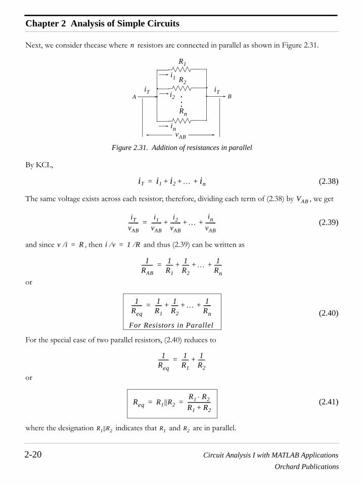
Chapter 2 Analysis of Simple Circuits
2-20 Circuit Analysis I with MATLAB ApplicationsOrchard Publications
Next, we consider thecase where resistors are connected in parallel as shown in Figure 2.31.
Figure 2.31. Addition of resistances in parallel
By KCL,
(2.38)
The same voltage exists across each resistor; therefore, dividing each term of (2.38) by , we get
(2.39)
and since , then and thus (2.39) can be written as
or
(2.40)
For the special case of two parallel resistors, (2.40) reduces to
or
(2.41)
where the designation indicates that and are in parallel.
n
..... .
.A B
R1
R2
Rn
iT iT
i1
i2
invAB
iT i1 i2 … in+ + +=
VAB
iTvAB--------
i1vAB--------
i2vAB-------- …
invAB--------+ + +=
v i⁄ R= i v⁄ 1 R⁄=
1RAB--------- 1
R1----- 1
R2----- … 1
Rn------+ + +=
1Req-------- 1
R1----- 1
R2----- … 1
Rn------+ + +=
For Resistors in Parallel
1Req-------- 1
R1----- 1
R2-----+=
Req R1 ||R2R1 R2⋅R1 R2+------------------= =
R1 ||R2 R1 R2

Circuit Analysis I with MATLAB Applications 2-21Orchard Publications
Resistance and Conductance Combinations
Also, since , from (2.38),
(2.42)
that is, parallel conductances combine as series resistors do.
Example 2.5
In the circuit of Figure 2.32,
a. Replace all resistors with a single equivalent resistance
b. Compute the voltage across the current source.
Figure 2.32. Circuit for Example 2.5
Solution:
a. We could use (2.40) to find the equivalent resistance . However, it is easier to form groups oftwo parallel resistors as shown in Figure 2.33 and use (2.41) instead.
Figure 2.33. Groups of parallel combinations for the circuit of Example 2.5.
Then,
G 1 R⁄=
Geq G1 G2 … Gn+ + + Gkk 1=
n
∑= =
Req
vAB
i
vAB
116
------ A
3 Ω 12 Ω 4 Ω 20 Ω
R1 R2 R3R4
R5
5 Ω
Req
i
116
------ A
vAB 3 Ω 12 Ω 4 Ω 20 Ω 5 ΩR1 R2 R3 R4 R5
R2||R312 4×12 4+--------------- 3 Ω= =

Chapter 2 Analysis of Simple Circuits
2-22 Circuit Analysis I with MATLAB ApplicationsOrchard Publications
Also,
and the circuit reduces to that shown in Figure 2.34.
Figure 2.34. Partial reduction for the circuit of Example 2.5
Next,
Finally,
and the circuit reduces to that shown in Figure 2.35
Figure 2.35. Reduction of the circuit of Example 2.5 to its simplest form
b. The voltage across the current source is
(2.43)
2.12 Voltage Division Expressions
In the circuit of Figure 2.36, , , and are known.
R4||R520 5×20 5+--------------- 4 Ω= =
i R1
vAB 3 Ω3 Ω
4 Ω116
------ A
3||3 3 3×3 3+------------ 1.5 Ω= =
Req 1.5 ||4 1.5 4×1.5 4+---------------- 12
11------ Ω= ==
i
116
------ A
vAB
Req
1211------ Ω
vAB
vAB IReq116
------ 1211------⋅ 2 V= = =
vS R1 R2

Circuit Analysis I with MATLAB Applications 2-23Orchard Publications
Voltage Division Expressions
Figure 2.36. Circuit for the derivation of the voltage division expressions
For the circuit of Figure 2.36, we will derive the voltage division expressions which state that:
These expressions enable us to obtain the voltage drops across the resistors in a series circuit simplyby observation.
Derivation:
By Ohm’s law in the circuit of Figure 2.36 where is the current flowing through i, we get
(2.44)
Also,
or
(2.45)
and by substitution of (2.45) into (2.44) we obtain the voltage division expressions below.
(2.46)
Example 2.6
In the network of Figure 2.37, the arrows indicate that resistors and are variable and that thepower supply is set for .
a. Compute and if and are adjusted for and respectively.
+−
vS
R2
R1
vR1R1
R1 R2+------------------vS and vR2
R2
R1 R2+------------------vS==
i
vR1 R1i and vR2 R2i==
R1 R2+( )i vS=
ivS
R1 R2+------------------=
vR1R1
R1 R2+------------------vS and vR2
R2
R1 R2+------------------vS==
VOLTAGE DIVISION EXPRESSIONS
R1 R2
12 V
vR1 vR2 R1 R2 7 Ω 5 Ω

Chapter 2 Analysis of Simple Circuits
2-24 Circuit Analysis I with MATLAB ApplicationsOrchard Publications
b. To what values should and be adjusted so that , , and?
Figure 2.37. Network for Example 2.6
Solution:
a. Using the voltage division expressions of (2.46), we get
and
b. Since , , and the voltage drops are proportional to theresistances, it follows that if we let and , the voltage drops and willbe and respectively.
2.13 Current Division Expressions
In the circuit shown in Figure 2.38, , , and are known.
Figure 2.38. Circuit for the derivation of the current division expressions
R1 R2 vR1 3 V= vR2 9 V=
R1 R2+ 12 Ω=
+
−
PowerSupply
(VoltageSource)
12 V
+
+
−
−
vR1
vR2
R1
R2
vR1R1
R1 R2+------------------vS
77 5+------------ 12× 7 V= = =
vR2R2
R1 R2+------------------vS
57 5+------------ 12× 5 V= = =
vR1 vR2+ 3 9+ 12 V= = R1 R2+ 12 Ω=
R1 3 Ω= R2 9 Ω= vR1 vR2
3 V 9 V
iS G1 G2
v
iSiG1
iG2G1 G2R1( ) R2( )

Circuit Analysis I with MATLAB Applications 2-25Orchard Publications
Current Division Expressions
For the circuit of Figure 2.38, we will derive the current division expressions which state that
and these expressions enable us to obtain the currents through the conductances (or resistances) ina parallel circuit simply by observation.
Derivation:
By Ohm’s law for conductances, we get
(2.47)
Also,
or
(2.48)
and by substitution of (2.48) into (2.47)
(2.49)
Also, since
by substitution into (2.49) we get
(2.50)
Example 2.7
For the circuit of figure 2.39, compute the voltage drop
Solution:
The current source divides into currents and as shown in Figure 2.40.
iG1G1
G1 G2+-------------------iS and iG2
G2
G1 G2+-------------------iS==
iG1 G1v and iG2 G2v==
G1 G2+( )v iS=
viS
G1 G2+-------------------=
iG1G1
G1 G2+-------------------iS and iG2
G2
G1 G2+-------------------iS==
R11
G1------= R2
1G2------=
iR1R2
R1 R2+------------------iS and iR2
R1
R1 R2+------------------iS==
CURRENT DIVISION EXPRESSIONS
v
iS i1 i2

Chapter 2 Analysis of Simple Circuits
2-26 Circuit Analysis I with MATLAB ApplicationsOrchard Publications
Figure 2.39. Circuit for Example 2.7
Figure 2.40. Application of current division expressions for the circuit of Example 2.7
We observe that the voltage is the voltage across the resistor . Therefore, we are only interestedin current . This is found by the current division expression as
and observing the passive sign convention, the voltage is
or
2.14 Standards for Electrical and Electronic Devices
Standardization of electronic components such as resistors, capacitors and diodes is carried out byvarious technical committees. In the United States, the Electronics Industries Association (EIA) andthe American National Standards Institute (ANSI) have established and published several standardsfor electrical and electronic devices to provide interchangeability among similar products made bydifferent manufacturers. Also, the U.S. Department of Defense or its agencies issue standards known
v
+
−
iS
R2R1
R3
R4
4 Ω
5 Ω
20 Ω
12 Ω3 A
v
+
−
iSR2
R1R3
R4
4 Ω
5 Ω
20 Ω
12 Ω
3 Ai2 i1
v R1
i1
i1R2 R3 R4+ +
R1 R2 R3 R4+ + +------------------------------------------- iS⋅ 4 5 20+ +
12 4 5 20+ + +------------------------------------- 3⋅ 87
41------ A= = =
v
v i1R1–8741------ 12⋅–
104441
------------ V–= = =
v 25.46 V–=
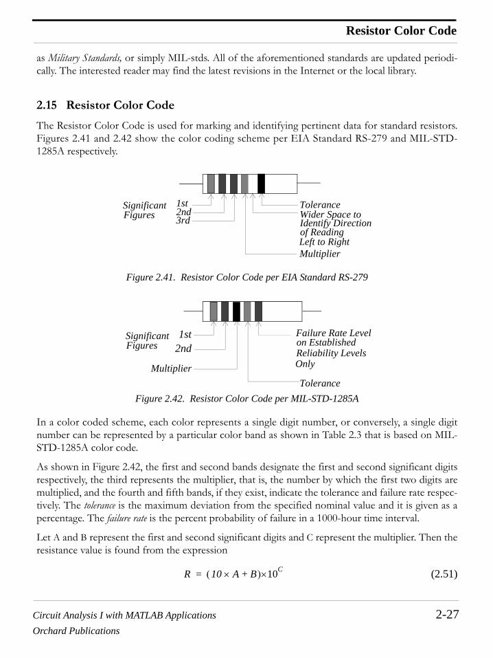
Circuit Analysis I with MATLAB Applications 2-27Orchard Publications
Resistor Color Code
as Military Standards, or simply MIL-stds. All of the aforementioned standards are updated periodi-cally. The interested reader may find the latest revisions in the Internet or the local library.
2.15 Resistor Color Code
The Resistor Color Code is used for marking and identifying pertinent data for standard resistors.Figures 2.41 and 2.42 show the color coding scheme per EIA Standard RS-279 and MIL-STD-1285A respectively.
Figure 2.41. Resistor Color Code per EIA Standard RS-279
Figure 2.42. Resistor Color Code per MIL-STD-1285A
In a color coded scheme, each color represents a single digit number, or conversely, a single digitnumber can be represented by a particular color band as shown in Table 2.3 that is based on MIL-STD-1285A color code.
As shown in Figure 2.42, the first and second bands designate the first and second significant digitsrespectively, the third represents the multiplier, that is, the number by which the first two digits aremultiplied, and the fourth and fifth bands, if they exist, indicate the tolerance and failure rate respec-tively. The tolerance is the maximum deviation from the specified nominal value and it is given as apercentage. The failure rate is the percent probability of failure in a 1000-hour time interval.
Let A and B represent the first and second significant digits and C represent the multiplier. Then theresistance value is found from the expression
(2.51)
1st 2nd
3rd
SignificantFigures
ToleranceWider Space toIdentify Directionof ReadingLeft to RightMultiplier
SignificantFigures
Tolerance
Multiplier
Failure Rate Levelon EstablishedReliability LevelsOnly
1st2nd
R 10 A B+×( ) C×10=
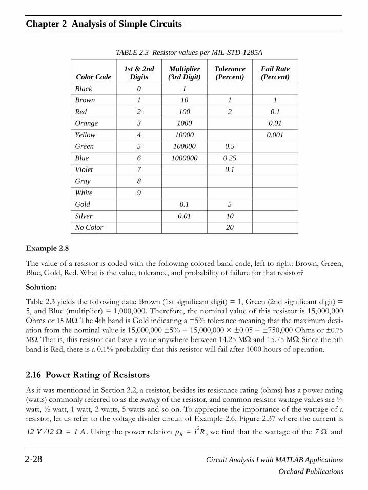
Chapter 2 Analysis of Simple Circuits
2-28 Circuit Analysis I with MATLAB ApplicationsOrchard Publications
Example 2.8
The value of a resistor is coded with the following colored band code, left to right: Brown, Green,Blue, Gold, Red. What is the value, tolerance, and probability of failure for that resistor?
Solution:
Table 2.3 yields the following data: Brown (1st significant digit) = 1, Green (2nd significant digit) =5, and Blue (multiplier) = 1,000,000. Therefore, the nominal value of this resistor is 15,000,000Ohms or 15 MΩ. The 4th band is Gold indicating a ±5% tolerance meaning that the maximum devi-ation from the nominal value is 15,000,000 ±5% = 15,000,000 × ±0.05 = ±750,000 Ohms or ±0.75MΩ. That is, this resistor can have a value anywhere between 14.25 MΩ and 15.75 MΩ. Since the 5thband is Red, there is a 0.1% probability that this resistor will fail after 1000 hours of operation.
2.16 Power Rating of Resistors
As it was mentioned in Section 2.2, a resistor, besides its resistance rating (ohms) has a power rating(watts) commonly referred to as the wattage of the resistor, and common resistor wattage values are ¼watt, ½ watt, 1 watt, 2 watts, 5 watts and so on. To appreciate the importance of the wattage of aresistor, let us refer to the voltage divider circuit of Example 2.6, Figure 2.37 where the current is
. Using the power relation , we find that the wattage of the and
TABLE 2.3 Resistor values per MIL-STD-1285A
Color Code1st & 2nd
DigitsMultiplier (3rd Digit)
Tolerance (Percent)
Fail Rate (Percent)
Black 0 1
Brown 1 10 1 1
Red 2 100 2 0.1
Orange 3 1000 0.01
Yellow 4 10000 0.001
Green 5 100000 0.5
Blue 6 1000000 0.25
Violet 7 0.1
Gray 8
White 9
Gold 0.1 5
Silver 0.01 10
No Color 20
12 V 12 Ω⁄ 1 A= pR i2R= 7 Ω
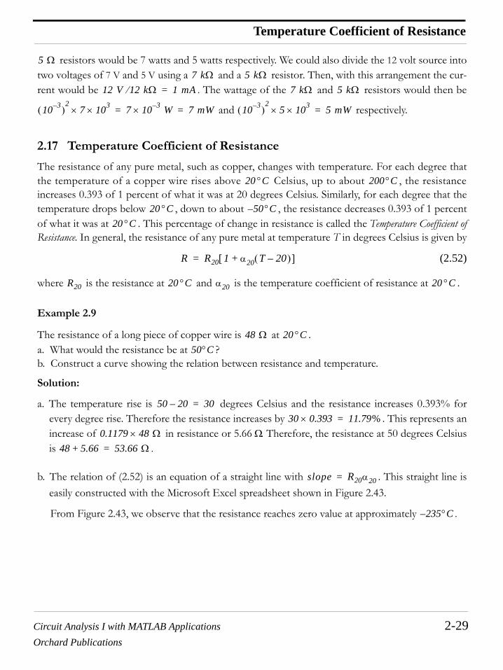
Circuit Analysis I with MATLAB Applications 2-29Orchard Publications
Temperature Coefficient of Resistance
resistors would be 7 watts and 5 watts respectively. We could also divide the 12 volt source intotwo voltages of 7 V and 5 V using a and a resistor. Then, with this arrangement the cur-rent would be . The wattage of the and resistors would then be
and respectively.
2.17 Temperature Coefficient of Resistance
The resistance of any pure metal, such as copper, changes with temperature. For each degree thatthe temperature of a copper wire rises above Celsius, up to about , the resistanceincreases 0.393 of 1 percent of what it was at 20 degrees Celsius. Similarly, for each degree that thetemperature drops below , down to about , the resistance decreases 0.393 of 1 percentof what it was at . This percentage of change in resistance is called the Temperature Coefficient ofResistance. In general, the resistance of any pure metal at temperature T in degrees Celsius is given by
(2.52)
where is the resistance at and is the temperature coefficient of resistance at .
Example 2.9
The resistance of a long piece of copper wire is at .a. What would the resistance be at ?b. Construct a curve showing the relation between resistance and temperature.
Solution:
a. The temperature rise is degrees Celsius and the resistance increases 0.393% forevery degree rise. Therefore the resistance increases by . This represents anincrease of in resistance or 5.66 Ω. Therefore, the resistance at 50 degrees Celsiusis .
b. The relation of (2.52) is an equation of a straight line with . This straight line iseasily constructed with the Microsoft Excel spreadsheet shown in Figure 2.43.
From Figure 2.43, we observe that the resistance reaches zero value at approximately .
5 Ω7 kΩ 5 kΩ
12 V 12 kΩ⁄ 1 mA= 7 kΩ 5 kΩ
10 3–( )2
7 103×× 7 10 3–× W 7 mW= = 10 3–( )2
5 103×× 5 mW=
20 °C 200 °C
20 °C 50– °C20 °C
R R20 1 α20 T 20–( )+[ ]=
R20 20 °C α20 20 °C
48 Ω 20 °C50°C
50 20– 30=
30 0.393× 11.79%=
0.1179 48 Ω×48 5.66+ 53.66 Ω=
slope R20α20=
235– °C

Chapter 2 Analysis of Simple Circuits
2-30 Circuit Analysis I with MATLAB ApplicationsOrchard Publications
Figure 2.43. Spreadsheet for construction of equation (2.52)
2.18 Ampere Capacity of Wires
For public safety, electric power supply (mains) wiring is controlled by local, state and federal boards,primarily on the National Electric Code (NEC) and the National Electric Safety Code. Moreover, manyproducts such as wire and cable, fuses, circuit breakers, outlet boxes and appliances are governed byUnderwriters Laboratories (UL) Standards which approves consumer products such as motors, radios,television sets etc.
Table 2.4 shows the NEC allowable current-carrying capacities for copper conductors based on thetype of insulation.
The ratings in Table 2.4 are for copper wires. The ratings for aluminum wires are typically 84% ofthese values. Also, these rating are for not more than three conductors in a cable with temperature
or . The NEC contains tables with correction factors at higher temperatures.
2.19 Current Ratings for Electronic Equipment
There are also standards for the internal wiring of electronic equipment and chassis. Table 2.5 pro-vides recommended current ratings for copper wire based on ( for wires smaller than 22AWG. Listed also, are the circular mils and these denote the area of the cross section of each wiresize. A circular mil is the area of a circle whose diameter is 1 mil (one-thousandth of an inch). Since thearea of a circle is proportional to the square of its diameter, and the area of a circle one mil in diame-ter is one circular mil, the area of any circle in circular mils is the square of its diameter in mils.
A mil-foot wire is a wire whose length is one foot and has a cross-sectional area of one circular mil.
Temp Resistance(deg C) (Ohms)
-250 -2.9328-240 -1.0464-230 0.84-220 2.7264-210 4.6128-200 6.4992-190 8.3856-180 10.272-170 12.1584-160 14.0448-150 15.9312-140 17.8176
Resistance of Copper Wire versus Temperature
0
20
40
60
80
100
-250 -200 -150 -100 -50 0 50 100 150 200 250
Degrees Celsius
Ohm
s
30°C 86°F
45°C 40°C

Circuit Analysis I with MATLAB Applications 2-31Orchard Publications
Current Ratings for Electronic Equipment
† Dry Locations Only ‡ Nickel or nickel-coated copper only
TABLE 2.4 Current Carrying Capacities for Copper Conductors
Copper Conductor Insulation
Size (AWG)
RUH(14-2)T, TW, UF
RH, RHW, RUH,(14-2)
THW, THWN,XHHW
TA, TBS, SA,FEP, FEPB,RHH, THHN
XHHW† TFE‡
14 15 15 25 4012 20 20 30 5510 30 30 40 758 40 45 50 956 55 65 70 1204 70 85 90 1453 80 100 105 1702 95 115 120 1951 110 130 140 2200 125 150 155 25000 145 175 185 280000 165 200 210 3150000 195 230 235 370

Chapter 2 Analysis of Simple Circuits
2-32 Circuit Analysis I with MATLAB ApplicationsOrchard Publications
The resistance of a wire of length can be computed by the relation
(2.53)
TABLE 2.5 Current Ratings for Electronic Equipment and Chassis Copper Wires
Wire Size Maximum Current (Amperes)
AWG Circular Mils
Nominal Resistance
(Ohms/1000 ft)at 100 °C
Wire in Free Air
Wire Confined in Insulation
32 63.2 188 0.53 0.32
30 100.5 116 0.86 0.5228 159.8 72 1.4 0.8326 254.1 45.2 2.2 1.324 404 28.4 3.5 2.122 642.4 22 7 520 10.22 13.7 11 7.518 1624 6.5 16 1016 2583 5.15 22 1314 4107 3.2 32 1712 6530 2.02 41 2310 10380 1.31 55 338 16510 0.734 73 466 26250 0.459 101 604 41740 0.29 135 802 66370 0.185 181 1001 83690 0.151 211 1250 105500 0.117 245 15000 133100 0.092 283 175000 167800 0.074 328 2000000 211600 0.059 380 225
l
R ρld2-----=

Circuit Analysis I with MATLAB Applications 2-33Orchard Publications
Copper Conductor Sizes for Interior Wiring
where = resistance per mil-foot, = length of wire in feet, = diameter of wire in mils, and isthe resistance at .
Example 2.10
Compute the resistance per mile of a copper conductor inch in diameter given that the resis-tance per mil-foot of copper is at .
Solution:
and from (2.53)
Column 3 of Table 2.5 shows the copper wire resistance at . Correction factors must beapplied to determine the resistance at other temperatures or for other materials. For copper, theconversion equation is
(2.54)
where is the resistance at the desired temperature, is the resistance at for copper,and is the desired temperature.
Example 2.11
Compute the resistance of of size copper wire at .
Solution:
From Table 2.5 we find that the resistance of of size copper wire at is. Then, by (2.54), the resistance of the same wire at is
2.20 Copper Conductor Sizes for Interior Wiring
In the design of an interior electrical installation, the electrical contractor must consider two impor-tant factors:
a. The wiring size in each section must be selected such that the current shall not exceed the cur-rent carrying capacities as defined by the NEC tables. Therefore, the electrical contractor mustaccurately determine the current which each wire must carry and make a tentative selection ofthe size listed in Table 2.4.
ρ l d R20 °C
1 8⁄10.4 Ω 20 °C
1 8⁄( ) in 0.125 in 125 mils= =
R ρld2----- 10.4 5280×
1252---------------------------- 3.51 Ω= = =
100°C
RT R100 1 0.004 T 100–( )+[ ]=
RT R100 100°C
T
1000 ft AWG 12 30°C
1000 ft AWG 12 100°C2.02 Ω 30°C
R30°C 2.02 1 0.004 30 100–( )+[ ] 1.45 Ω= =

Chapter 2 Analysis of Simple Circuits
2-34 Circuit Analysis I with MATLAB ApplicationsOrchard Publications
b. The voltage drop throughout the electrical system must then be computed to ensure that it doesnot exceed certain specifications. For instance, in the lighting part of the system referred to as thelighting load, a variation of more than in the voltage across each lamp causes an unpleasantvariation in the illumination. Also, the voltage variation in the heating and air conditioning loadmust not exceed .
Important! The requirements stated here are for instructional purposes only. They change fromtime to time. It is, therefore, imperative that the designer consults the latest publicationsof the applicable codes for compliance.
Example 2.12
Figure 2.44 shows a lighting load distribution diagram for an interior electric installation.
Figure 2.44. Load distribution for an interior electric installation
The panel board is 200 feet from the meter. Each of the three branches has 12 outlets for 75 w, 120volt lamps. The load center is that point on the branch line at which all lighting loads may be consid-ered to be concentrated. For this example, assume that the distance from the panel to the load centeris 60 ft. Compute the size of the main lines. Use T (thermoplastic insulation) type copper conductorand base your calculations on temperature environment.
Solution:
It is best to use a spreadsheet for the calculations so that we can compute sizes for more and differ-ent branches if need be.
The computations for Parts I and II are shown on the spreadsheet of Figure 2.45 where from the lastline of Part II we see that the percent line drop is and this is more than twice the allowable drop. With the voltage variation the brightness of the lamps would vary through wideranges, depending on how many lamps were in use at one time.
5%
10%
kw-hrMeter
PanelBoard
L1
L2
L3
CircuitBreaker
UtilityCompanySwitch
Branch Lines
MainLines
LightingLoad
25°C
12.29 5%12.29%

Circuit Analysis I with MATLAB Applications 2-35Orchard Publications
Copper Conductor Sizes for Interior Wiring
A much higher voltage than the rated would cause these lamps to glow far above their ratedcandle power and would either burn them immediately, or shorten their life considerably. It is there-fore necessary to install larger than main line. The computations in Parts III through V ofthe spreadsheet of Figures 2.45 and 2.46 indicate that we should not use a conductor less than size
.
120 V
12 AWG
6 AWG

Chapter 2 Analysis of Simple Circuits
2-36 Circuit Analysis I with MATLAB ApplicationsOrchard Publications
Figure 2.45. Spreadsheet for Example 2.12, Parts I and II
Part
ISi
zing
in A
ccor
danc
e w
ith N
EC (T
able
2.2
)S
tep
Des
crip
tion
Cal
cula
tion
Val
ueU
nits
1M
eter
to P
anel
Boa
rd D
ista
nce
200
ft2
No.
of B
ranc
hes
from
Pan
el B
oard
33
Out
lets
per
bra
nch
124
Out
let V
olta
ge R
atin
g12
0V
5P
ower
dra
wn
from
eac
h ou
tlet
75w
6P
ower
requ
ired
by e
ach
bran
chS
tep
3 x
Ste
p 5
900
w7
Cur
rent
dra
wn
by e
ach
bran
chS
tep
6 / S
tep
47.
50A
8R
equi
red
wire
siz
e fo
r bra
nche
s *
Tabl
e 2.
414
AW
GC
arrie
s up
to 1
5 A
9C
urre
nt re
quire
d by
the
mai
n lin
eS
tep
2 x
Ste
p 7
22.5
0A
10R
equi
red
wire
siz
e fo
r mai
n lin
eTa
ble
2.4
12A
WG
Car
ries
up to
20
A
Part
IIC
heck
for V
olta
ge D
rops
11D
ista
nce
from
pan
el to
load
cen
ter
60ft
12N
umbe
r of w
ires
in e
ach
bran
ch2
13To
tal l
engt
h of
wire
in e
ach
bran
chS
tep
11 x
Ste
p 12
120
ft14
Spe
cifie
d Te
mpe
ratu
re in
0 C25
0 C15
Res
ista
nce
of 1
000
ft 14
AW
G w
ire a
t 100
0 CTa
ble
2.5
3.20
Ω16
Res
ista
nce
of 1
000
ft 14
AW
G w
ire a
t Spe
c. T
emp
Equ
atio
n (2
.54)
2.24
Ω17
Res
ista
nce
of a
ctua
l len
gth
of w
ire(S
tep
13 x
Ste
p 16
) / 1
000
0.26
9Ω
18V
olta
ge d
rop
in e
ach
bran
chS
tep
7 x
Ste
p 17
2.02
V19
Num
ber o
f wire
s in
eac
h m
ain
220
Tota
l len
gth
of w
ire in
mai
n lin
eS
tep
1 x
Ste
p 19
400
ft21
Res
ista
nce
of 1
000
ft 12
AW
G w
ire a
t 100
0 CTa
ble
2.5
2.02
Ω22
Res
ista
nce
of 1
000
ft 12
AW
G w
ire a
t Spe
c. T
emp
Equ
atio
n (2
.54)
1.41
Ω23
Res
ista
nce
of a
ctua
l len
gth
of w
ire(S
tep
20 x
Ste
p 22
) /10
000.
57Ω
24V
olta
ge d
rop
in m
ain
line
Ste
p 9
x S
tep
2312
.73
V25
Vol
tage
dro
p fro
m m
eter
to lo
ad c
ente
rS
tep
18 +
Ste
p 24
14.7
4V
26P
erce
nt li
ne d
rop
(Ste
p 25
/ S
tep
4) x
100
12.2
9%
* N
o si
ze s
mal
ler c
an b
e in
stal
led;
sm
alle
r siz
es
have
insu
ffici
ent m
echa
nica
l stre
ngth

Circuit Analysis I with MATLAB Applications 2-37Orchard Publications
Copper Conductor Sizes for Interior Wiring
Figure 2.46. Spreadsheet for Example 2.12, Parts III, IV, and V
Part
IIIR
ecal
cula
tion
Usi
ng 1
0 A
WG
Con
duct
or S
ize
27N
ext l
arge
r con
duct
or s
ize
for m
ain
line
Tabl
e 2.
410
AW
GC
arrie
s up
to 3
0 A
28R
esis
tanc
e of
100
0 ft
10 A
WG
wire
at 1
00 0 C
Tabl
e 2.
51.
310
Ω29
Res
ista
nce
of 1
000
ft 10
AW
G w
ire a
t Spe
c. T
emp
Equ
atio
n (2
.54)
0.91
7Ω
30R
esis
tanc
e of
act
ual l
engt
h of
wire
(Ste
p 20
x S
tep
29)/1
000
0.36
7Ω
31V
olta
ge d
rop
in m
ain
line
Ste
p 9
x S
tep
308.
25V
32V
olta
ge d
rop
from
met
er to
load
cen
ter
Ste
p 18
+ S
tep
2410
.27
V
33P
erce
nt li
ne d
rop
(Ste
p 32
/ S
tep
4) x
100
8.56
%
Part
IVR
ecal
cula
tion
Usi
ng 8
AW
G C
ondu
ctor
Siz
e
34N
ext l
arge
r con
duct
or s
ize
for m
ain
line
Tabl
e 2.
48
AW
GC
arrie
s up
to 4
0 A
35R
esis
tanc
e of
100
0 ft
8 A
WG
wire
at 1
00 0 C
Tabl
e 2.
50.
734
Ω36
Res
ista
nce
of 1
000
ft 8
AW
G w
ire a
t Spe
c. T
emp
Equ
atio
n (2
.54)
0.51
4Ω
37R
esis
tanc
e of
act
ual l
engt
h of
wire
(Ste
p 20
x S
tep
36)/1
000
0.20
6Ω
38V
olta
ge d
rop
in m
ain
line
Ste
p 9
x S
tep
374.
62V
39V
olta
ge d
rop
from
met
er to
load
cen
ter
Ste
p 18
+ S
tep
386.
64V
40P
erce
nt li
ne d
rop
(Ste
p 39
/ S
tep
4) x
100
5.53
%
Part
VR
ecal
cula
tion
Usi
ng 6
AW
G C
ondu
ctor
Siz
e
41N
ext l
arge
r con
duct
or s
ize
for m
ain
line
Tabl
e 2.
46
AW
GC
arrie
s up
to 5
5 A
42R
esis
tanc
e of
100
0 ft
6 A
WG
wire
at 1
00 0 C
Tabl
e 2.
50.
459
Ω43
Res
ista
nce
of 1
000
ft 6
AW
G w
ire a
t Spe
c. T
emp
Equ
atio
n (2
.54)
0.32
1Ω
44R
esis
tanc
e of
act
ual l
engt
h of
wire
(Ste
p 20
x S
tep
43)/1
000
0.12
9Ω
45V
olta
ge d
rop
in m
ain
line
Ste
p 9
x S
tep
442.
89V
46V
olta
ge d
rop
from
met
er to
load
cen
ter
Ste
p 18
+ S
tep
454.
91V
47P
erce
nt li
ne d
rop
(Ste
p 46
/ S
tep
4) x
100
4.09
%

Chapter 2 Analysis of Simple Circuits
2-38 Circuit Analysis I with MATLAB ApplicationsOrchard Publications
2.21 Summary
• Ohm’s Law states that the voltage across a device is proportional to the current through thatdevice and the resistance is the constant of proportionality.
• Open circuit refers to an open branch (defined below) in a network. It can be thought of as a resis-tor with infinite resistance (or zero conductance). The voltage across the terminals of an openmay have a finite value or may be zero whereas the current is always zero.
• Short circuit refers to a branch (defined below) in a network that contains no device between itsterminals, that is, a piece of wire with zero resistance. The voltage across the terminals of a short isalways zero whereas the current may have a finite value or may be zero.
• A resistor absorbs power.
• A resistor does not store energy. The energy is dissipated in the form of heat.
• A node is a common point where one end of two or more devices are connected.
• A branch is part of a network that contains a device and its nodes.
• A mesh is a closed path that does not contain other closed paths
• A loop contains two or more closed paths.
• Kirchoff ’s Current Law (KCL) states that the algebraic sum of the currents entering (or leaving) anode is zero.
• Kirchoff ’s Voltage Law (KVL) states that the algebraic sum of the voltage drops (or voltage rises)around a closed mesh or loop is zero.
• Two or more devices are said to be connected in series if and only if the same current flowsthrough them.
• Two or more devices are said to be connected in parallel if and only if the same voltage existsacross their terminals.
• A series circuit with a single mesh can be easily analyzed by KVL.
• A parallel circuit with a single node pair can be easily analyzed by KCL.
• If two or more voltage sources are in series, they can be replaced by a single voltage source withthe proper polarity.
• If two or more current sources are in parallel, they can be replaced by a single current source withthe proper current direction.
• If two or more resistors are connected in series, they can be replaced by an equivalent resistancewhose value is

Circuit Analysis I with MATLAB Applications 2-39Orchard Publications
Summary
• If two or more resistors are connected in parallel, they can be replaced by an equivalent resis-tance whose value is
• For the special case of two parallel resistors, the equivalent resistance is found from the relation
• Conductances connected in series combine as resistors in parallel do.
• Conductances connected in parallel combine as resistors in series do.
• For the simple series circuit below
the voltage division expressions state that:
• For the simple parallel circuit below
the current division expressions state that:
Req R1 R2 R3 … Rn+ + + + RKk 1=
n
∑= =
1Req-------- 1
R1----- 1
R2----- … 1
Rn------+ + +=
Req R1||R2R1 R2⋅R1 R2+------------------= =
+−
vS
R2
R1
vR1R1
R1 R2+------------------vS and vR2
R2
R1 R2+------------------vS==
v
iSiR1
iR2R1 R2
iR1R2
R1 R2+------------------ iS and iR2
R1
R1 R2+------------------ iS==

Chapter 2 Analysis of Simple Circuits
2-40 Circuit Analysis I with MATLAB ApplicationsOrchard Publications
• In the United States, the Electronics Industries Association (EIA) and the American NationalStandards Institute (ANSI) have established and published several standards for electrical and elec-tronic devices to provide interchangeability among similar products made by different manufactur-ers.
• The resistor color code is used for marking and identifying pertinent data for standard resistors.Two standards are the EIA Standard RS-279 and MIL-STD-1285A.
• Besides their resistance value, resistors have a power rating.
• The resistance of a wire increases with increased temperature and decreases with decreased tem-perature.
• The current ratings for wires and electronic equipment are established by national standards andcodes.

Circuit Analysis I with MATLAB Applications 2-41Orchard Publications
Exercises
2.22 Exercises
Multiple Choice
1. Ohm’s Law states that
A. the conductance is the reciprocal of resistance
B. the resistance is the slope of the straight line in a voltage versus current plot
C. the resistance is the sum of the voltages across all the devices in a closed path divided by thesum of the currents through all the devices in the closed path
D. the sum of the resistances around a closed loop is zero
E. none of the above
2. Kirchoff ’s Current Law (KCL) states that
A. the sum of the currents in a closed path is zero
B. the current that flows through a device is inversely proportional to the voltage across thatdevice
C. the sum of the currents through all the devices in a closed path is equal to the sum of the volt-ages across all the devices
D. the sum of the currents entering a node is equal to the sum of the currents leaving that node
E. none of the above
3. Kirchoff ’s Voltage Law (KCL) states that
A. the voltage across a device is directly proportional to the current through that device
B. the voltage across a device is inversely proportional to the current through that device
C. the sum of the voltages across all the devices in a closed path is equal to the sum of the cur-rents through all the devices
D. the sum of the voltages in a node is equal to the sum of the currents at that node
E. none of the above
4. For the three resistors connected as shown on the network of Figure 2.47, the equivalent resis-tance is computed with the formula
A.
B.
RAB
RAB R1 R2+ R3+=
RAB R12 R2
2+ R32+=

Chapter 2 Analysis of Simple Circuits
2-42 Circuit Analysis I with MATLAB ApplicationsOrchard Publications
C.
D.
E. none of the above
Figure 2.47. Network for Question 4
5. For the three conductances connected as shown on the network of Figure 2.48, the equivalentconductance is computed with the formula
A.
B.
C.
D.
E. none of the above
Figure 2.48. Network for Question 5
6. For the three resistances connected as shown on the network of Figure 2.49, the equivalent con-ductance is
A.
B.
RABR1R2R3
R1 R2 R3+ +-------------------------------=
RABR1R2R3
R1 R2 R3+ +-------------------------------=
A BR1 R2
R3
RAB
GAB
GAB G1 G2+ G3+=
GAB G12 G2
2+ G32+=
GABG1G2G3
G1 G2+ G3+---------------------------------=
1GAB---------- 1
G1------ 1
G2------ 1
G3------+ +=
A BG1 G2
G3
GAB
GAB
21 Ω 1–
1.5 Ω 1–

Circuit Analysis I with MATLAB Applications 2-43Orchard Publications
Exercises
C.
D.
E. none of the above
Figure 2.49. Network for Question 6
7. In the network shown in Figure 2.50, when , the voltage . When ,. When , is
A.
B.
C.
D.
E. none of the above
Figure 2.50. Network for Question 7
8. The node voltages shown in the partial network of Figure 2.51 are relative to some referencenode not shown. The value of the voltage is
A.
B.
C.
D.
2 3⁄ Ω 1–
144 19⁄ Ω 1–
GAB 4 Ω 12 Ω 3 Ω
R1 R2 R3
A
B
R 4 Ω= vR 6 V= R 0 Ω=
iR 2 A= R ∞= vR
6 V
24 V
8 V
16 V
+
−
vRRest of the
Circuit
iR
R
vX
6– V
16 V
0 V
10 V

Chapter 2 Analysis of Simple Circuits
2-44 Circuit Analysis I with MATLAB ApplicationsOrchard Publications
E. none of the above
Figure 2.51. Network for Question 8
9. For the network of Figure 2.52 the value of the voltage is
A.
B.
C.
D.
E. none of the above
Figure 2.52. Network for Question 9
10. For the circuit of Figure 2.53 the value of the current is
A.
B.
C.
D.
E. none of the above
+− 8 V2 A
10 V
2 A 3 Ω
20 V
4 Ω6 V8 Ω
2 VvX
v
8 V
2 V
2– V
8– V
+−8 V
4 Ωv
+
−
i
2 A
0 A
∞ A
1 A

Circuit Analysis I with MATLAB Applications 2-45Orchard Publications
Exercises
Figure 2.53. Network for Question 10
Problems
1. In the circuit of Figure 2.54, the voltage source and both resistors are variable.
Figure 2.54. Circuit for Problem 1
a. With , , and , compute the power absorbed by .
Answer:
b. With and , to what value should be adjusted so that the powerabsorbed by it will be 200 w? Answer:
c. With and , to what value should be adjusted to so that the powerabsorbed by will be 100 w? Answer:
2. In the circuit of Figure 2.55, represents the load of that circuit.
Figure 2.55. Circuit for Problem 2
+−8 V
12 Ωi
4 Ω
+
−
PowerSupply
(VoltageSource)
+
+
−
−vS
R1
R2
vS 120 V= R1 70 Ω= R2 50 Ω= R2
50 w
vS 120 V= R1 0 Ω= R2
72 Ω
R1 0 Ω= R2 100 Ω= vS
R2 100 V
RLOAD
+−
+ −
75 V
24 V5 A
3 A
+
−
iLOAD
pLOADvLOAD
RLOAD
5 Ω
10 Ω
2 Ω

Chapter 2 Analysis of Simple Circuits
2-46 Circuit Analysis I with MATLAB ApplicationsOrchard Publications
Compute:
a. Answer:
b. Answer:
c. Answer:
3. For the circuit of Figure 2.56, compute the power supplied or absorbed by each device.
Figure 2.56. Circuit for Problem 3
Answers: , , , ,
4. In the circuit of Figure 2.57, compute the power delivered or absorbed by the dependent voltagesource.
Figure 2.57. Circuit for Problem 4
Answer:
5. In the network of Figure 2.58, each resistor is 10 Ω. Compute the equivalent resistance .
iLOAD 8 A
vLOAD 20 V
pLOAD 160 w
A
B
C
D
E+
−
+
−
+
−
6 A24 A
12 V 60 V 36 V
pA 288 w= pB 1152 w= pC 1800– w= pD 144 w= pE 216 w=
+−
+−
50 V
10 A
5iR2 V
R4
R3
R2
R1 10 Ω
6 Ω
2 Ω
10 Ω
iR2
62.5 w
Req

Circuit Analysis I with MATLAB Applications 2-47Orchard Publications
Exercises
Figure 2.58. Circuit for Problem 5
Answer:
6. In the network of Figure 2.59, and . Compute the current i supplied bythe 15 V source.
Figure 2.59. Circuit for Problem 6
Hint: Start at the right end and by series and parallel combinations of the resistors, reduce the cir-cuit to a simple series circuit. This method is known as analysis by network reduction.Answer:
7. In the circuit of Figure 2.60, use the voltage division expression to compute and .
Figure 2.60. Circuit for Problem 7
Answers: ,
Req
360 21 Ω⁄
R1 10 Ω= R2 20 Ω=
+−
15 V
R1 R1 R1R1R1R1R1
R1R2R2R2R2R2R2
i
0.75 A
vX vY
+−
16 V
5 Ω 20 Ω
10 Ω 40 Ω
+−
24 V
−
+
−
+
vX
vY
vX 8 3 V⁄= vY 16– 3 V⁄=

Chapter 2 Analysis of Simple Circuits
2-48 Circuit Analysis I with MATLAB ApplicationsOrchard Publications
8. In the circuit of Figure 2.61, use the current division expression to compute and .
Figure 2.61. Circuit for Problem 8
Answers: ,
9. A transformer consists of two separate coils (inductors) wound around an iron core as shown in Figure2.62. There are many turns in both the primary and secondary coils but, for simplicity, only feware shown. It is known that the primary coil has a resistance of 5.48 Ω at 20 degrees Celsius. Aftertwo hours of operation, it is found that the primary coil resistance has risen to 6.32 Ω. Computethe temperature rise of this coil.
Figure 2.62. Circuit for Problem 9
Answer:
10. A new facility is to be constructed at a site which is 1.5 miles away from the nearest electric utilitycompany substation. The electrical contractor and the utility company have made load calcula-tions, and decided that the main lines from the substation to the facility will require several cop-per conductors in parallel. Each of these conductors must have insulation type THHN and mustcarry a maximum current of 220 A in a temperature environment.
a. Compute the voltage drop on each of these conductors from the substation to the facility whenthey carry the maximum required current of 220 A in a temperature environment.Answer:
iX iY
16 A 24 A
5 Ω
20 Ω
10 Ω
40 Ω
iX iY
iX 16– 3 V⁄= iY 8– 3 V⁄=
PrimaryCoil
Iron Core
SecondaryCoil
36°C
20 °C
20 °C70 V

Circuit Analysis I with MATLAB Applications 2-49Orchard Publications
Exercises
b. The power absorbed by each conductor under the conditions stated above.Answer:
c. The power absorbed per square cm of the surface area of each conductor under the conditionsstated above.Answer:
15.4 Kw
0.02 w cm2⁄

Chapter 2 Analysis of Simple Circuits
2-50 Circuit Analysis I with MATLAB ApplicationsOrchard Publications
2.23 Answers to Exercises
Multiple Choice
1. B
2. D
3. E
4. E
5. D
6. C
7. B When , the voltage . Therefore, . Also, when ,
, and thus (short circuit). When , but has a finite value
and it is denoted as in the figure below. Now, we observe that the triangles abc and dbe
are similar. Then or and thus
8. D We denote the voltage at the common node as shown on the figure of the next page. Then,
from the branch that contains the resistor, we observe that or and
thus
R 4 Ω= vR 6 V= iR 6 4⁄ 1.5 A= = R 0 Ω=
iR 2 A= vR 0= R ∞= iR 0= vR
vR ∞=
bebc------ de
ac------= 2.0 1.5–
2.0--------------------- 6
vR ∞=--------------= vR ∞= 24 V=
iR A( )
vR V( )
0.5 2.01.51.0
6.0
a
bc
d
e
vR ∞=
vA
3 ΩvA 10–
3----------------- 2= vA 16=
vX 6– 16+ 10 V= =

Circuit Analysis I with MATLAB Applications 2-51Orchard Publications
Answers to Exercises
9. A This is an open circuit and therefore no current flows through the resistor. Accordingly, thereis no voltage drop across the resistor and thus .
10. A The resistor is shorted out by the short on the right side of the circuit and thus the onlyresistance in the circuit is the resistor.
Problems
1. a. With , , and , the circuit is as shown below.
Using the voltage division expression, we get
Then,
b. With and , the circuit is as shown below.
We observe that
+− 8 V2 A
10 V
2 A 3 Ω
20 V
4 Ω6 V8 Ω
2 V vX
vA
v 8 V=
12 Ω4 Ω
vS 120 V= R1 70 Ω= R2 50 Ω=
+−
vS
R2
R150 Ω
70 Ω
120 V
vR2
5070 50+------------------ 120× 50 V= =
pR2
vR2
2
R2------- 502
50-------- 50 w= = =
vS 120 V= R1 0 Ω=
+−
vS
R2
R150 Ω
0 Ω
120 V
vR2vs 120V= =

Chapter 2 Analysis of Simple Circuits
2-52 Circuit Analysis I with MATLAB ApplicationsOrchard Publications
and
or
or
c. With and , the circuit is as shown below.
Then,
or
or
or
2. a. Application of KCL at node A of the circuit below yields
b. Application of KVL around Mesh 1 yields
vR2
2
R2------- 200 w=
1202
R2----------- 200 w=
R21202
200----------- 72 Ω= =
R1 0 Ω= R2 100 Ω=
+−
vS
R2
R1100 Ω
0 Ω
vS2
R2------ 100 w=
vS2
100--------- 100 w=
vS2 100 100× 10 000,= =
vS 10 000, 100 V= =
iLOAD 3 5+ 8 A= =
75– 3 5( ) vAB+ + 0=

Circuit Analysis I with MATLAB Applications 2-53Orchard Publications
Answers to Exercises
or
Application of KVL around Mesh 2 yields
or
or
c.
3. Where not shown, we assign plus (+) and minus (−) polarities and current directions in accor-dance with the passive sign convention as shown below.
We observe that and . Also, by KCL at Node X
Then,
+−
+ −
75 V
24 V5 A
3 A
+
−
iLOAD
pLOADvLOAD
RLOAD
5 Ω
10 Ω
2 Ω
iLOAD
Mesh 1 Mesh 2
A
B
vAB 60 V=
vAB 24 2iLOAD+ +– vLOAD+ 0=
60– 24 2 8× vLOAD+ + + 0=
vLOAD 20 V=
pLOAD vLOAD iLOAD× 20 8× 160 w absorbed power( )= = =
A
B
C
D
E+
−
+
−
+
−
6 A24 A
12 V 60 V 36 V
+ +− −
iAiC iE
iB iD
vA
vBvC
vDvE
X
iA iB= iE iD=
iC iB iD+ 24 6+ 30 A= = =
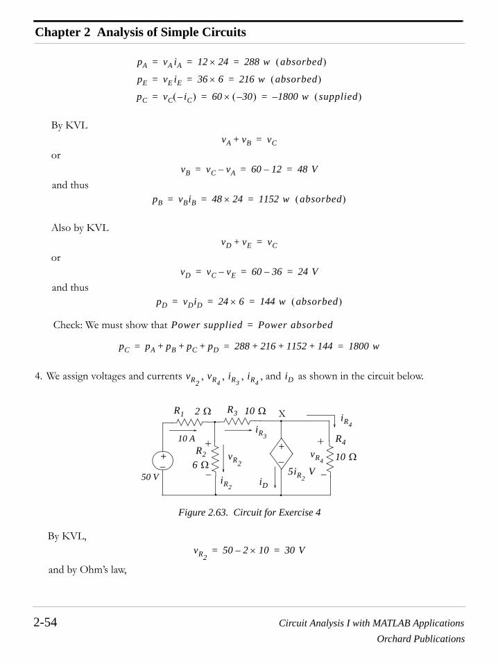
Chapter 2 Analysis of Simple Circuits
2-54 Circuit Analysis I with MATLAB ApplicationsOrchard Publications
By KVL
or
and thus
Also by KVL
or
and thus
Check: We must show that
4. We assign voltages and currents , , , , and as shown in the circuit below.
Figure 2.63. Circuit for Exercise 4
By KVL,
and by Ohm’s law,
pA vA iA 12 24× 288 w absorbed( )= = =
pE vE iE 36 6× 216 w absorbed( )= = =
pC vC iC–( ) 60 30–( )× 1800– w supplied( )= = =
vA vB+ vC=
vB vC vA– 60 12– 48 V= = =
pB vBiB 48 24× 1152 w absorbed( )= = =
vD vE+ vC=
vD vC vE– 60 36– 24 V= = =
pD vDiD 24 6× 144 w absorbed( )= = =
Power supplied Power absorbed=
pC pA pB pC pD+ + + 288 216 1152 144+ + + 1800 w= = =
vR2vR4
iR3iR4
iD
+−
+−
50 V
10 A
iR2
5iR2 V
R4
R3
R2
R1 10 Ω
6 Ω
2 Ω
10 Ω+ +
− −
vR2vR4
iR3
iD
iR4X
vR250 2 10×– 30 V= =

Circuit Analysis I with MATLAB Applications 2-55Orchard Publications
Answers to Exercises
Therefore, the value of the dependent voltage source is
and
Then,
By KCL at Node X
where
and thus
with the indicated direction through the dependent source. Therefore,
5. The simplification procedure starts with the resistors in parallel which are indicated below.
iR2
vR2R2------- 30
6------ 5 A= = =
5iR25 5× 25 V= =
vR45iR2
25 V= =
iR4
vR4
R4------- 25
10------ 2.5 A= = =
iD iR3iR4
–=
iR310 iR2
– 10 5– 5 A= = =
iD iR3iR4
– 5 2.5– 2.5 A= = =
pD 5iR2iD 25 2.5× 62.5 w absorbed( )= = =
Req Req
10 10
1010
1010
10
10
10
10
10
10
10 10
10 10
10
10
10 10
5 5
5 5

Chapter 2 Analysis of Simple Circuits
2-56 Circuit Analysis I with MATLAB ApplicationsOrchard Publications
6. We start with the right side of the circuit where the last two resistors are in series as shown below.
Then,
Next,
and so on. Finally, addition of the left most resistor with its series equivalent yields
and thus
Req
10
10
1010
5 15
5 15
Req
10
6
610
5
5
Req
16
16
5
5
Req Req
180 21⁄
180 21⁄
360 21⁄
+−
15 V
R1 R1 R1R1R1R1R1
R1R2R2R2R2R2R2
i
R1 R1+ 10 10+ 20 Ω= =
20 20|| 10 Ω=
10 10+ 20 Ω=
10 10+ 20 Ω=
i 15 20⁄ 0.75 A= =

Circuit Analysis I with MATLAB Applications 2-57Orchard Publications
Answers to Exercises
7. We first simplify the given circuit by replacing the parallel resistors by their equivalents. Thus,
and
The voltage sources are in series opposing connection and they can be replaced by a single volt-age source with value . The simplified circuit is shown below.
Now, by the voltage division expression,
and
or
Check: By application of KVL starting at point A and going counterclockwise, we get
8. We first simplify the given circuit by replacing the series resistors by their equivalents. Thus,
and
The current sources are in parallel opposing connection and they can be replaced by a single cur-rent source with value . The simplified circuit is shown below.
5 20|| 5 20×5 20+--------------- 4 Ω= =
10 40|| 10 40×10 40+------------------ 8 Ω= =
24 16– 8 V=
4 Ω
8 Ω
+−
8 V
−
+
−
+
vX
vY
iA
vX4
4 8+------------ 8× 8
3--- V= =
v– Y8
4 8+------------ 8× 16
3------ V= =
vY163
------– V=
vX vY–( ) 8–+ 83--- 16
3------ 8–+ 0= =
5 20+ 25 Ω=
10 40+ 50 Ω=
24 16– 8 A=

Chapter 2 Analysis of Simple Circuits
2-58 Circuit Analysis I with MATLAB ApplicationsOrchard Publications
By the current division expression,
and
Check: By application of KCL starting at point and going counterclockwise, we get
9. We construct the resistance versus temperature plot shown below.
From the similar triangles acd and abe, we get
or
10. a. From Table 2.4 we find that the cable size must be 0000 AWG and this can carry up to .Also, from Table 2.5 we find that the resistance of this conductor is at
. Then, the resistance of this conductor that is 1.5 miles long is
8 A25 Ω 50 Ω
iX iY
iX50
25 50+------------------ 8–( )× 16
3------– A= =
iY25
25 50+------------------ 8–( )× 8
3---– A= =
A
8 iX iY+ + 8 163------– 8
3---– 0= =
0−234.5
R20R0
RX
T °C( )
R Ω( )
T20 TX
a
b
c
de
R20 5.48 Ω=
RX 6.32 Ω=
TX ∆T=T20 20°C=
RXR20--------
234.5 T20 TX+ +
234.5 T20+----------------------------------------
234.5 20 TX+ +
234.5 20+--------------------------------------
254.5 TX+
254.5--------------------------= = =
∆T TX=RXR20-------- 254.5× 254.5–
6.325.48---------- 254.5× 254.5– 36°C= = =
235 A0.059 Ω 1000 ft⁄
100°C

Circuit Analysis I with MATLAB Applications 2-59Orchard Publications
Answers to Exercises
To find the resistance of this cable at , we use the relation of (2.54). Thus,
and the voltage drop on each of these conductors is
b. The power absorbed by each conductor is
c. Table 2.5 gives wire sizes in circular mils. We recall that a circular mil is the area of a circlewhose diameter is . To find the diameter in cm, we perform the following conversion:
From Table 2.5 we find that the cross section of a cable is 211,600 circular mils.
Then, the cross-section of this cable in is
Therefore, the cable diameter in cm is
The cross-section circumference of the cable is
and the surface area of the cable is
Then, the power absorbed per is
0.059 Ω1000ft---------------- 5280
1 mile----------------× 1.5 miles× 0.4673 Ω at 100°C=
20°C
R20 R100 1 0.004 20 100–( )+[ ] 0.4673 1 0.32–( ) 0.3178 Ω= = =
v iR 220 0.3178× 70 V= = =
p vi 70 220× 15 400 w, 15.4 Kw= = = =
0.001 in
1 circular mil π4---d2 π
4--- 0.001( )2 7.854 10 7– in2×= = =
7.854 10 7– in2× 2.54 cm( )2
in2---------------------------× 5.067 10 6–× cm2==
0000 AWG
cm2
211 600 circular mils 5.067 10 6–× cm2
circular mil------------------------------------------×, 1.072 cm2=
d 1.072= 1.035 cm=
πd π 1.035× 3.253 cm= =
Surface area πdl 3.253 cm 1.5 miles 1.609 Km1 mile
------------------------ 105 cm1 Km
-----------------××× 7.851 105 cm2×= = =
cm2
pcm2
Total powercm2
-------------------------------- 15 400 w,
7.851 105 cm2×---------------------------------------- 0.02 w cm2⁄= = =

Chapter 2 Analysis of Simple Circuits
2-60 Circuit Analysis I with MATLAB ApplicationsOrchard Publications
NOTES

Circuit Analysis I with MATLAB Applications 3-1Orchard Publications
Chapter 3
Nodal and Mesh Equations - Circuit Theorems
his chapter begins with nodal, loop and mesh equations and how they are applied to the solu-tion of circuits containing two or more node-pairs and two or more loops or meshes. Othertopics included in this chapter are the voltage-to-current source transformations and vice
versa, Thevenin’s and Norton’s theorems, the maximum power transfer theorem, linearity, superposi-tion, efficiency, and regulation.
3.1 Nodal, Mesh, and Loop Equations
Network Topology is a branch of network theory concerned with the equations required to completelydescribe an electric circuit. In this text, we will only be concerned with the following two theorems.
Theorem 3.1
Let ; then independent nodal equations are required tocompletely describe that circuit. These equations are obtained by setting the algebraic sum of thecurrents leaving each of the nodes equal to zero.
Theorem 3.2
Let , , ina circuit; then independent loop or mesh equations are required to completelydescribe that circuit. These equations are obtained by setting the algebraic sum of the voltage dropsaround each of the loops or meshes equal to zero.
3.2 Analysis with Nodal Equations
In writing nodal equations, we perform the following steps:
1. For a circuit containing N nodes, we choose one of these as a reference node assumed to be zerovolts or ground.
2. At each non-reference node we assign node voltages where each of these voltagesis measured with respect to the chosen reference node, i.e., ground.
3. If the circuit does not contain any voltage sources between nodes, we apply KCL and write anodal equation for each of the node voltages .
T
N number of nodes in a circuit= N 1–
N 1–
L M number of loops or meshes= = B number of branches= N number of nodes=
L M B N– 1+= =
L M B N– 1+= =
v1 v2 … vn 1–, , ,
v1 v2 … vn 1–, , ,

Chapter 3 Nodal and Mesh Equations - Circuit Theorems
3-2 Circuit Analysis I with MATLAB ApplicationsOrchard Publications
4. If the circuit contains a voltage source between two nodes, say nodes j and k denoted as node vari-ables and , we replace the voltage source with a short circuit thus forming a combined nodeand we write a nodal equation for this common node in terms of both and ; then we relatethe voltage source to the node variables and .
Example 3.1
Write nodal equations for the circuit shown in Figure 3.1, and solve for the unknowns of these equa-tions using matrix theory, Cramer’s rule, or the substitution method. Verify your answers withExcel® or MATLAB®. Please refer to Appendix A for discussion and examples.
Figure 3.1. Circuit for Example 3.1
Solution:
We observe that there are 4 nodes and we denote these as , , , and (for ground) as shown inFigure 3.2.
Figure 3.2. Circuit for Example 3.1
For convenience, we have denoted the currents with a subscript that corresponds to the resistorvalue through which it flows through; thus, the current that flows through the resistor isdenoted as , the current through the resistor is denoted as , and so on. We will follow thispractice in the subsequent examples.
vj vk
vj vk
vj vk
12 A 24 A18 A
4 Ω
8 Ω 10 Ω
6 Ω
G
12 A 24 A18 A
G
v1 v2v3
i4
i8 i10
i64 Ω 6 Ω
10 Ω8 Ω
4 Ωi4 8 Ω i8

Circuit Analysis I with MATLAB Applications 3-3Orchard Publications
Analysis with Nodal Equations
For the circuit of Figure 3.2, we need nodal equations. Let us choose node G(ground) as our reference node, and we assign voltages , and at nodes , , and respec-tively; these are to be measured with respect to the ground node G. Now, application of KCL atnode yields
or
(3.1)
where is the current flowing from left to right. Expressing (3.1) in terms of the node voltages, weget
or
or
(3.2)
Next, application of KCL at node yields
or
(3.3)
where is the current flowing from right to left * and is the current that flows from left toright.
* The direction of the current through the 8 Ω resistor from left to right in writing the nodal equation at Node 1,and from right to left in writing the nodal equation at Node 2, should not be confusing. Remember that we wroteindependent node equations at independent nodes and, therefore, any assumptions made in writing the firstequation need not be held in writing the second since the latter is independent of the first. Of course, we couldhave assumed that the current through the 8 Ω resistor flows in the same direction in both nodal equations. It isadvantageous, however, to assign a (+) sign to all currents leaving the node in which we apply KCL. The advan-tage is that we can check, or even write the node equations by inspection. With reference to the above circuit andequation (3.1) for example, since G = 1/R, we denote the coefficients of v1 (1/4 and 1/8 siemens) as self conduc-tances and the coefficient of v2 (−1/8) as mutual conductance. Likewise, in equation (3.3) the coefficients of v2(1/8 and 1/10 siemens) are the self conductances and the coefficients of v1 (−1/8) and v3 (−1/10) are the mutualconductances. Therefore, we can write a nodal equation at a particular node by inspection, that is, we assignplus (+) values to self conductances and minus (−) to mutual conductances.
N 1– 4 1– 3= =
v1 v2, v3
i4 i8 12–+ 0=
i4 i8+ 12=
i8
v14-----
v1 v2–
8----------------+ 12=
14--- 1
8---+⎝ ⎠
⎛ ⎞ v118---v2– 12=
3v1 v2– 96=
i8 i10 18+ + 0=
i8 i10+ 18–=
i8 i10

Chapter 3 Nodal and Mesh Equations - Circuit Theorems
3-4 Circuit Analysis I with MATLAB ApplicationsOrchard Publications
Expressing (3.3) in terms of node voltages, we get
or
or
(3.4)
Similarly, application of KCL at node yields
or
where is the current flowing from right to left. Then, in terms of node voltages,
(3.5)
or
or
or
(3.6)
Equations (3.2), (3.4), and (3.6) constitute a set of three simultaneous equations with threeunknowns. We write them in matrix form as follows:
(3.7)
v2 v1–
8----------------
v2 v3–
10----------------+ 18–=
18---v1– 1
8--- 1
10------+⎝ ⎠
⎛ ⎞ v2110------v3–+ 18–=
5v1 9v2– 4v3+ 720=
i10 i6 24–+ 0=
i10 i6+ 24=
i10
v3 v2–
10----------------
v36-----+ 24=
110------v2– 1
10------ 1
6---+⎝ ⎠
⎛ ⎞ v3+ 24=
3v2– 18v3+ 720=
v2 6– v3 240–=
3 1– 05 9– 40 1 6–
G
v1
v2
v3
V
96720240–
I
=
⎧ ⎪ ⎨ ⎪ ⎩ ⎧ ⎨ ⎩ ⎧ ⎨ ⎩

Circuit Analysis I with MATLAB Applications 3-5Orchard Publications
Analysis with Nodal Equations
We can use Cramer’s rule or Gauss’s elimination method as discussed in Appendix A, to solve (3.7)for the unknowns. Simultaneous solution yields , , and . Withthese values we can determine the current in each resistor, and the power absorbed or delivered byeach device.
Check with MATLAB®:
G=[3 −1 0; 5 −9 4; 0 1 −6]; I=[96 720 -240]'; V=G\I;...fprintf(' \n'); fprintf('v1 = %5.2f volts \t', V(1)); ...fprintf('v2 = %5.2f volts \t', V(2)); fprintf('v3 = %5.2f volts', V(3)); fprintf(' \n')
v1 = 12.00 volts v2 = -60.00 volts v3 = 30.00 volts
Check with Excel®:
The spreadsheet of Figure 3.3 shows the solution of the equations of (3.7). The procedure is dis-cussed in Appendix A.
Figure 3.3. Spreadsheet for the solution of (3.7)
Example 3.2
For the circuit of Figure 3.4, write nodal equations in matrix form and solve for the unknowns usingmatrix theory, Cramer’s rule, or Gauss’s elimination method. Verify your answers with Excel orMATLAB. Please refer to Appendix A for procedures and examples. Then construct a table show-ing the voltages across, the currents through and the power absorbed or delivered by each device.
Solution:
We observe that there are 4 nodes and we denote these as , , , and (for ground) as shown inFigure 3.5.
v1 12 V= v2 60– V= v3 30 V=
123456789
A B C D E F G HSpreadsheet for Matrix Inversion and Matrix Multiplication
3 -1 0 96G= 5 -9 4 I= 720
0 1 -6 -240
0.417 -0.050 -0.033 12G-1= 0.250 -0.150 -0.100 V= -60
0.042 -0.025 -0.183 30
G
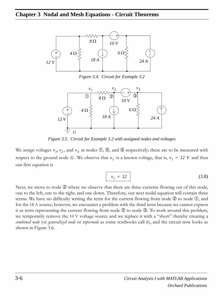
Chapter 3 Nodal and Mesh Equations - Circuit Theorems
3-6 Circuit Analysis I with MATLAB ApplicationsOrchard Publications
Figure 3.4. Circuit for Example 3.2
Figure 3.5. Circuit for Example 3.2 with assigned nodes and voltages
We assign voltages , and at nodes , , and respectively; these are to be measured withrespect to the ground node . We observe that is a known voltage, that is, and thusour first equation is
(3.8)
Next, we move to node where we observe that there are three currents flowing out of this node,one to the left, one to the right, and one down. Therefore, our next nodal equation will contain threeterms. We have no difficulty writing the term for the current flowing from node to node , andfor the 18 A source; however, we encounter a problem with the third term because we cannot expressit as term representing the current flowing from node to node . To work around this problem,we temporarily remove the 10 V voltage source and we replace it with a “short” thereby creating acombined node (or generalized node or supernode as some textbooks call it), and the circuit now looks asshown in Figure 3.6.
12 V 24 A18 A
4 Ω 6 Ω
8 Ω
+
− +
−
10 V
12 V 24 A18 A
4 Ω 6 Ω
8 Ω
+
− +
−
10 V
G
v1 v2 v3
v1 v2, v3
G v1 v1 12 V=
v1 12=
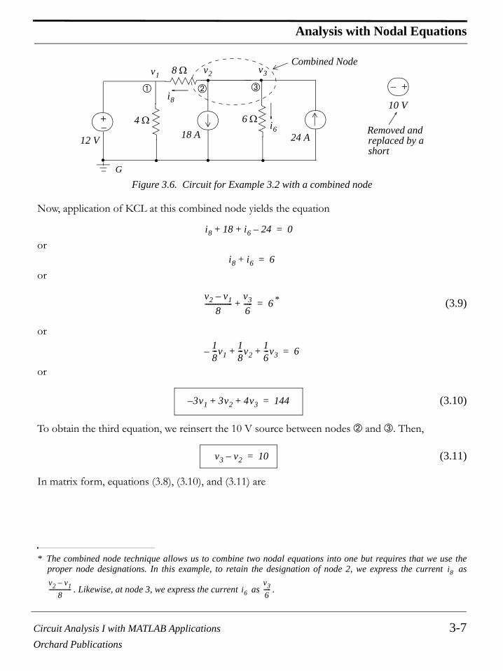
Circuit Analysis I with MATLAB Applications 3-7Orchard Publications
Analysis with Nodal Equations
Figure 3.6. Circuit for Example 3.2 with a combined node
Now, application of KCL at this combined node yields the equation
or
or
* (3.9)
or
or
(3.10)
To obtain the third equation, we reinsert the 10 V source between nodes and . Then,
(3.11)
In matrix form, equations (3.8), (3.10), and (3.11) are
* The combined node technique allows us to combine two nodal equations into one but requires that we use theproper node designations. In this example, to retain the designation of node 2, we express the current as
. Likewise, at node 3, we express the current as .
12 V 24 A18 A
4 Ω 6 Ω
8 Ω
+−
G
v1 v2 v3
i8
i6
Combined Node
− +
10 V
Removed andreplaced by ashort
i8 18 i6 24–+ + 0 =
i8 i6+ 6=
v2 v1–
8----------------
v36-----+ 6=
i8
v2 v1–
8---------------- i6
v36-----
18---v1–
18---v2
16---v3+ + 6=
3v1 3v2 4v3+ +– 144=
v3 v2– 10=

Chapter 3 Nodal and Mesh Equations - Circuit Theorems
3-8 Circuit Analysis I with MATLAB ApplicationsOrchard Publications
(3.12)
Simultaneous solution yields , , and . From these we can find thecurrent through each device and the power absorbed or delivered by each device.
Check with MATLAB:
G=[1 0 0; −3 3 4; 0 −1 1]; I=[12 144 10]'; V=G\I;...fprintf(' \n'); fprintf('v1 = %5.2f volts \t', V(1)); ...fprintf('v2 = %5.2f volts \t', V(2)); fprintf('v3 = %5.2f volts', V(3)); fprintf(' \n')
v1 = 12.00 volts v2 = 20.00 volts v3 = 30.00 volts
Check with Excel:
Figure 3.7. Spreadsheet for the solution of (3.12)
Table 3.1 shows that the power delivered is equal to the power absorbed.
3.3 Analysis with Mesh or Loop Equations
In writing mesh or loop equations, we follow these steps:
1. For a circuit containing meshes (or loops), we assign a mesh or loop current for each mesh or loop.
2. If the circuit does not contain any current sources, we apply KVL around each mesh or loop.
1 0 03– 3 4
0 1– 1
G
v1
v2
v3
V
1214410
I
=
⎧ ⎪ ⎪ ⎨ ⎪ ⎪ ⎩ ⎧ ⎨ ⎩ ⎧ ⎨ ⎩
v1 12 V= v2 20 V= v3 30 V=
123456789
A B C D E F G HSpreadsheet for Matrix Inversion and Matrix Multiplication
1 0 0 12G= -3 3 4 I= 144
0 -1 1 10
1.000 0.000 0.000 12G-1= 0.429 0.143 -0.571 V= 20
0.429 0.143 0.429 30
M L B N– 1+= =
i1 i2 … in 1–, , ,

Circuit Analysis I with MATLAB Applications 3-9Orchard Publications
Analysis with Mesh or Loop Equations
3. If the circuit contains a current source between two meshes or loops, say meshes or loops j and kdenoted as mesh variables and , we replace the current source with an open circuit thusforming a common mesh or loop, and we write a mesh or loop equation for this common meshor loop in terms of both and . Then, we relate the current source to the mesh or loop vari-ables and .
Example 3.3
For the circuit of Figure 3.8, write mesh equations in matrix form and solve for the unknowns usingmatrix theory, Cramer’s rule, or Gauss’s elimination method. Verify your answers with Excel orMATLAB. Please refer to Appendix A for procedures and examples. Then construct a table show-ing the voltages across, the currents through, and the power absorbed or delivered by each device.
Figure 3.8. Circuit for Example 3.3
TABLE 3.1 Table for Example 3.2
Power (watts)
Device Voltage (volts) Current (amps) Delivered Absorbed12 V Source 12 2 2410 V Source 10 19 19018 A Source 20 18 36024 A Source 30 24 7204 Ω Resistor 12 3 366 Ω Resistor 30 5 1508 Ω Resistor 8 1 8Total 744 744
ij ik
ij ikij ik
12 V
24 V
36 V 8 Ω
+−+−
+ −
+−
2 Ω
4 Ω 6 Ω 12 Ω
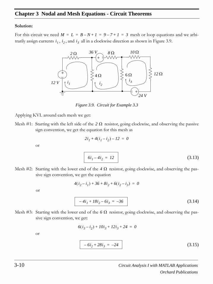
Chapter 3 Nodal and Mesh Equations - Circuit Theorems
3-10 Circuit Analysis I with MATLAB ApplicationsOrchard Publications
Solution:
For this circuit we need mesh or loop equations and we arbi-trarily assign currents , , and all in a clockwise direction as shown in Figure 3.9.
Figure 3.9. Circuit for Example 3.3
Applying KVL around each mesh we get:
Mesh #1: Starting with the left side of the resistor, going clockwise, and observing the passivesign convention, we get the equation for this mesh as
or
(3.13)
Mesh #2: Starting with the lower end of the resistor, going clockwise, and observing the pas-sive sign convention, we get the equation
or
(3.14)
Mesh #3: Starting with the lower end of the resistor, going clockwise, and observing the pas-sive sign convention, we get:
or
(3.15)
M L B N– 1+ 9 7– 1+ 3= = = =
i1 i2 i3
12 V
24 V
36 V 8 Ω
+−+−
+ −
+−
2 Ω 10 Ω
4 Ω 6 Ω 12 Ω
i1 i2i3
2 Ω
2i1 4 i1 i2–( ) 12–+ 0=
6i1 4i2– 12=
4 Ω
4 i2 i1–( ) 36 8i2+ + 6 i2 i3–( )+ 0=
4i1– 18i2 6i3–+ 36–=
6 Ω
6 i3 i2–( ) 10i3 12i3 24+ + + 0=
6i2– 28i3+ 24–=
Circuit Analysis I with MATLAB Applications 3-11Orchard Publications
Analysis with Mesh or Loop Equations
Note: For this example, we assigned all three currents with the same direction, i.e., clockwise. This,of course, was not mandatory; we could have assigned any direction in any mesh. It is advantageous,however, to assign the same direction to all currents. The advantage here is that we can check, oreven write the mesh equations by inspection. This is best explained with the following observations:
1. With reference to the circuit of Figure 3.9 and equation (3.13), we see that current flowsthrough the and resistors. We call these the self resistances of the first mesh. Their sum,i.e., is the coefficient of current in that equation. We observe that current alsoflows through the resistor. We call this resistance the mutual resistance between the first andthe second mesh. Since enters the lower end of the resistor, and in writing equation(3.13) we have assumed that the upper end of this resistor has the plus (+) polarity, then inaccordance with the passive sign convention, the voltage drop due to current is and thisis the second term on the left side of (3.13).
2. In Mesh 2, the self resistances are the , , and resistors whose sum, 18, is the coeffi-cient of in equation (3.14). The and resistors are also the mutual resistances betweenthe first and second, and the second and the third meshes respectively. Accordingly, the voltagedrops due to the mutual resistances in the second equation have a minus (-) sign, i.e, and
.
3. The signs of the coefficients of and in (3.15) are similarly related to the self and mutualresistances in the third mesh.
Simplifying and rearranging (3.13), (3.14) and (3.15) we get:
(3.16)
(3.17)
(3.18)
and in matrix form
(3.19)
Simultaneous solution yields , , and where the negative val-ues for and indicate that the actual direction for these currents is counterclockwise.
i1
2 Ω 4 Ω2 4+ 6= i1 i2
4 Ωi2 4 Ω
i2 4i2–
4 Ω 8 Ω 6 Ωi2 4 Ω 6 Ω
4i1–
6i3–
i2 i3
3i1 2i2– 6=
2i1 9– i2 3i3+ 18=
3i2 14– i3 12=
3 2– 02 9– 30 3 14–
R
i1
i2
i3
I
61812
V
=
⎧ ⎪ ⎪ ⎨ ⎪ ⎪ ⎩ ⎧ ⎨ ⎩ ⎧ ⎨ ⎩
i1 0.4271= i2 2.3593–= i3 1.3627–=
i2 i3

Chapter 3 Nodal and Mesh Equations - Circuit Theorems
3-12 Circuit Analysis I with MATLAB ApplicationsOrchard Publications
Check with MATLAB:
R=[3 −2 0; 2 −9 3; 0 3 −14]; V=[6 18 12]'; I=R\V;...fprintf(' \n'); fprintf('i1 = %5.2f amps \t', I(1)); ...fprintf('i2 = %5.2f amps \t', I(2)); fprintf('i3 = %5.2f amps', I(3)); fprintf(' \n')
i1 = 0.43 amps i2 = -2.36 amps i3 = -1.36 amps
Excel produces the same answers as shown in Figure 3.10.
Figure 3.10. Spreadsheet for the solution of (3.19)
Table 3.2 shows that the power delivered by the voltage sources is equal to the power absorbed bythe resistors.
TABLE 3.2 Table for Example 3.3
Power (watts)Device Voltage (volts) Current (amps) Delivered Absorbed
12 V Source 12.000 0.427 5.12436 V Source 36.000 2.359 84.92424 V Source 24.000 1.363 32.7122 Ω Resistor 0.854 0.427 0.3654 Ω Resistor 11.144 2.786 30.9648 Ω Resistor 18.874 2.359 44.5306 Ω Resistor 5.976 0.996 5.95210 Ω Resistor 13.627 1.363 18.57012 Ω Resistor 16.352 1.363 22.288Total 122.760 122.669
123456789
A B C D E F G HSpreadsheet for Matrix Inversion and Matrix Multiplication
3 -2 0 6R= 2 -9 3 V= 18
0 3 -14 12
0.397 -0.095 -0.020 0.4271R-1= 0.095 -0.142 -0.031 I= -2.3593
0.020 -0.031 -0.078 -1.3627

Circuit Analysis I with MATLAB Applications 3-13Orchard Publications
Analysis with Mesh or Loop Equations
Example 3.4
For the circuit of Figure 3.11, write loop equations in matrix form, and solve for the unknownsusing matrix theory, Cramer’s rule, or Gauss’s elimination method. Verify your answers with Excelor MATLAB. Please refer to Appendix A for procedures and examples. Then, construct a tableshowing the voltages across, the currents through and the power absorbed or delivered by eachdevice.
Figure 3.11. Circuit for Example 3.4
Solution:
This is the same circuit as that of the previous example where we found that we need 3 mesh orloop equations. We choose our loops as shown in Figure 3.12, and we assign currents , , and ,all in a clockwise direction.
Figure 3.12. Circuit for Example 3.4 with assigned loops
Applying of KVL around each loop, we get:
Loop 1 (abgh): Starting with the left side of the resistor and complying with the passive signconvention, we get:
12 V
24 V
36 V 8 Ω
+−+−
+ −
+−
2 Ω 10 Ω
4 Ω 6 Ω 12 Ω
i1 i2 i3
12 V
24 V
36 V 8 Ω
+−+−
+ −
+−
2 Ω 10 Ω
4 Ω 6 Ω 12 Ωi1i2i3
ab c d
e
fgh
2 Ω
2 i1 i2 i3+ +( ) 4i1 12–+ 0=

Chapter 3 Nodal and Mesh Equations - Circuit Theorems
3-14 Circuit Analysis I with MATLAB ApplicationsOrchard Publications
or
or
(3.20)
Loop 2 (abcfgh): As before, starting with the left side of the resistor and complying with thepassive sign convention, we get:
or
or
(3.21)
Loop 3 (abcdefgh): Likewise, starting with the left side of the resistor and complying with thepassive sign convention, we get:
or
or
(3.22)
and in matrix form
(3.23)
Solving with MATLAB we get:
R=[3 1 1; 1 8 5; 1 5 16]; V=[6 −12 −24]'; I=R\V;...fprintf(' \n'); fprintf('i1 = %5.2f amps \t', I(1)); ...fprintf('i2 = %5.2f amps \t', I(2)); fprintf('i3 = %5.2f amps', I(3)); fprintf(' \n')
i1 = 2.79 amps i2 = -1.00 amps i3 = -1.36 amps
6i1 2i2 2i3+ + 12=
3i1 i2 i3+ + 6=
2 Ω
2 i1 i2 i3+ +( ) 36 8 i2 i3+( ) 6i2 12–+ + + 0=
2i1 16i2 10i3+ + 24–=
i1 8i2 5i3+ + 12–=
2 Ω
2 i1 i2 i3+ +( ) 36 8 i2 i3+( ) 10i3+ + + 12i3 24 12–+ + 0=
2i1 10i2 32i3+ + 48–=
i1 5i2 16i3+ + 24–=
3 1 11 8 51 5 16
R
i1
i2
i3
I
612–
24–
V
=
⎧ ⎪ ⎨ ⎪ ⎩ ⎧ ⎨ ⎩ ⎧ ⎨ ⎩

Circuit Analysis I with MATLAB Applications 3-15Orchard Publications
Analysis with Mesh or Loop Equations
Excel produces the same answers.
Table 3.3 shows that the power delivered by the voltage sources is equal to the power absorbed bythe resistors and the values are approximately the same as those of the previous example.
Example 3.5
For the circuit of figure 3.13, write mesh equations in matrix form and solve for the unknownsusing matrix theory, Cramer’s rule, or the substitution method. Verify your answers with Excel orMATLAB. Please refer to Appendix A for procedures and examples.
Figure 3.13. Circuit for Example 3.5
TABLE 3.3 Table for Example 3.4
Power (watts)
Device Voltage (volts) Current (amps) Delivered Absorbed12 V Source 12.000 0.427 5.12436 V Source 36.000 2.359 84.92424 V Source 24.000 1.363 32.7122 Ω Resistor 0.854 0.427 0.3654 Ω Resistor 11.146 2.786 31.0538 Ω Resistor 18.872 2.359 44.5196 Ω Resistor 5.982 0.997 5.96410 Ω Resistor 13.627 1.363 18.57412 Ω Resistor 16.352 1.363 22.283Total 122.760 122.758
12 V
36 V 8 Ω
+−+−
+ −
2 Ω 10 Ω
4 Ω 6 Ω 12 Ω
5 A

Chapter 3 Nodal and Mesh Equations - Circuit Theorems
3-16 Circuit Analysis I with MATLAB ApplicationsOrchard Publications
Solution:
This is the same circuit as those of the two previous examples except that the 24 V voltage sourcehas been replaced by a 5 A current source. As before, we need mesh or loop equations, and we assign currents , , and all in a clockwise direction as shown inFigure 3.14.
Figure 3.14. Circuit for Example 3.5 with assigned currents
For Meshes 1 and 2, the equations are the same as in Example 3.3 where we found them to be
or
(3.24)
and
or
(3.25)
For Mesh 3, we observe that the current is just the current of the 5 A current source and thus ourthird equation is simply
(3.26)
and in matrix form,
M L B N– 1+ 9 7– 1+ 3= = = =
i1 i2 i3
12 V
36 V 8 Ω
+−+−
+ −
2 Ω 10 Ω
4 Ω 6 Ω 12 Ω
5 A
i1 i2i3
6i1 4i2– 12=
3i1 2i2– 6=
4i1– 18i2 6i3–+ 36–=
2i1 9– i2 3i3+ 18=
i3
i3 5=
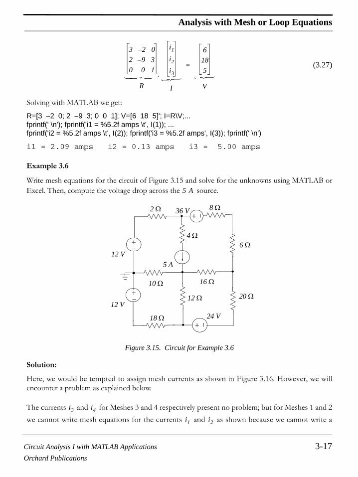
Circuit Analysis I with MATLAB Applications 3-17Orchard Publications
Analysis with Mesh or Loop Equations
(3.27)
Solving with MATLAB we get:
R=[3 −2 0; 2 −9 3; 0 0 1]; V=[6 18 5]'; I=R\V;...fprintf(' \n'); fprintf('i1 = %5.2f amps \t', I(1)); ...fprintf('i2 = %5.2f amps \t', I(2)); fprintf('i3 = %5.2f amps', I(3)); fprintf(' \n')
i1 = 2.09 amps i2 = 0.13 amps i3 = 5.00 amps
Example 3.6
Write mesh equations for the circuit of Figure 3.15 and solve for the unknowns using MATLAB orExcel. Then, compute the voltage drop across the source.
Figure 3.15. Circuit for Example 3.6
Solution:
Here, we would be tempted to assign mesh currents as shown in Figure 3.16. However, we willencounter a problem as explained below.
The currents and for Meshes 3 and 4 respectively present no problem; but for Meshes 1 and 2we cannot write mesh equations for the currents and as shown because we cannot write a
3 2– 02 9– 30 0 1
R
i1
i2
i3
I
6185
V
=
⎧ ⎪ ⎨ ⎪ ⎩ ⎧ ⎨ ⎩ ⎧ ⎨ ⎩
5 A
12 V
5 A
36 V 8 Ω
+−+−
+ −2 Ω
20 Ω
4 Ω6 Ω
12 Ω12 V
+−+−
24 V
+ −
10 Ω 16 Ω
18 Ω
i3 i4
i1 i2

Chapter 3 Nodal and Mesh Equations - Circuit Theorems
3-18 Circuit Analysis I with MATLAB ApplicationsOrchard Publications
term which represents the voltage across the current source. To work around this problem wetemporarily remove (open) the current source and we form a “combined mesh” (or generalized meshor supermesh as some textbooks call it) and the current that flows around this combined mesh is asshown in Figure 3.17.
Figure 3.16. Circuit for Example 3.6 with erroneous current assignments
Figure 3.17. Circuit for Example 3.6 with correct current assignments
Now, we apply KVL around this combined mesh. We start at the left end of the resistor, and weexpress the voltage drop across this resistor as since in Mesh 1 the current is essentially .
5 A5 A
12 V5 A
36 V 8 Ω
+−+−
+ −
2 Ω
20 Ω
4 Ω6 Ω
12 Ω12 V
+−+−
24 V+ −+ −
10 Ω 16 Ω
18 Ω
i1i2
i3 i4
12 V
36 V 8 Ω
+−+−
+ −
2 Ω
20 Ω
4 Ω6 Ω
12 Ω12 V
+−+−
24 V+ −+ −
10 Ω 16 Ω
18 Ω
CombinedMesh
i3i4
2 Ω2i1 i1

Circuit Analysis I with MATLAB Applications 3-19Orchard Publications
Analysis with Mesh or Loop Equations
Continuing, we observe that there is no voltage drop across the resistor since no current flowsthrough it. The current now enters Mesh 2 where we encounter the 36 V drop due to the voltagesource there, and the voltage drops across the and resistors are and respectivelysince in Mesh 2 the current now is really . The voltage drops across the and resistorsare expressed as in the previous examples and thus our first mesh equation is
or
or
(3.28)
Now, we reinsert the 5 A current source between Meshes 1 and 2 and we obtain our second equa-tion as
(3.29)
For meshes 3 and 4, the equations are
or
(3.30)
and
or
(3.31)
and in matrix form
(3.32)
We find the solution of (3.32) with the following MATLAB code.
4 Ω
8 Ω 6 Ω 8i2 6i2
i2 16 Ω 10 Ω
2i1 36 8i2 6i2 16 i2 i4–( ) 10 i1 i3–( ) 12–+ + + + + 0=
12i1 30i2 10– i3 16– i4+ 24–=
6i1 15i2 5– i3 8– i4+ 12–=
i1 i2– 5=
10 i3 i1–( ) 12 i3 i4–( ) 18i3 12–+ + 0=
5i1 20– i3 6i4+ 6–=
16 i4 i2–( ) 20i4 24–+ 12 i4 i3–( )+ 0=
4i2 3i3 12– i4+ 6–=
6 15 5– 8–
1 1– 0 05 0 20– 60 4 3 12–
R
i1
i2
i3
i4
I
12–
56–
6–
V
=
⎧ ⎪ ⎪ ⎪ ⎨ ⎪ ⎪ ⎪ ⎩ ⎧ ⎨ ⎩ ⎧ ⎨ ⎩
Chapter 3 Nodal and Mesh Equations - Circuit Theorems
3-20 Circuit Analysis I with MATLAB ApplicationsOrchard Publications
R=[6 15 −5 −8; 1 −1 0 0; 5 0 −20 6; 0 4 3 −12]; V=[−12 5 −6 −6]'; I=R\V;...fprintf(' \n');...fprintf('i1 = %5.4f amps \t',I(1)); fprintf('i2 = %5.4f amps \t',I(2));...fprintf('i3 = %5.4f amps \t',I(3)); fprintf('i4 = %5.4f amps',I(4)); fprintf(' \n')
i1=3.3975 amps i2=-1.6025 amps i3=1.2315 amps i4=0.2737 amps
Now, we can find the voltage drop across the current source by application of KVL aroundMesh 1 using the following relation:
This yields
We can verify this value by application of KVL around Mesh 2 where starting with the lower end ofthe resistor and going counterclockwise we get
With these values, we can also compute the power delivered or absorbed by each of the voltagesources and the current source.
3.4 Transformation between Voltage and Current Sources
In the previous chapter we stated that a voltage source maintains a constant voltage between its ter-minals regardless of the current that flows through it. This statement applies to an ideal voltagesource which, of course, does not exist; for instance, no voltage source can supply infinite current toa short circuit. We also stated that a current source maintains a constant current regardless of the ter-minal voltage. This statement applies to an ideal current source which also does not exist; forinstance, no current source can supply infinite voltage when its terminals are open-circuited.
A practical voltage source has an internal resistance which, to be accounted for, it is represented with anexternal resistance in series with the voltage source as shown in Figure 3.18 (a). Likewise apractical current source has an internal conductance which is represented as a resistance (or conduc-tance ) in parallel with the current source as shown in Figure 3.18 (b).
5 A
2 3.3975× 4 3.3975 1.6025+( )× v5A 10 3.3975 1.2315–( )× 12–+ + + 0=
v5A 36.455–=
6 w
6 8+( ) 1.6025 36– 4 3.3975 1.6025+( )×+× 36.455– 16 1.6025 0.2737+( )×+ 0=
RS vS
Rp
Gp iS
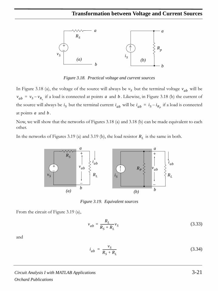
Circuit Analysis I with MATLAB Applications 3-21Orchard Publications
Transformation between Voltage and Current Sources
Figure 3.18. Practical voltage and current sources
In Figure 3.18 (a), the voltage of the source will always be but the terminal voltage will be if a load is connected at points and . Likewise, in Figure 3.18 (b) the current of
the source will always be but the terminal current will be if a load is connected
at points and .
Now, we will show that the networks of Figures 3.18 (a) and 3.18 (b) can be made equivalent to eachother.
In the networks of Figures 3.19 (a) and 3.19 (b), the load resistor is the same in both.
Figure 3.19. Equivalent sources
From the circuit of Figure 3.19 (a),
(3.33)
and
(3.34)
+−+−
(a) (b)
a
b
a
b
vS iS
RS
Rp
vS vab
vab vS vRs–= a b
iS iab iab iS iRP–=
a b
RL
+−+−
(a) (b)
a
b
a
b
+ +
− −
RL RLvS iS
RS
vab
iabRP vab
iab
vabRL
RS RL+-------------------= vS
iabvS
RS RL+-------------------=

Chapter 3 Nodal and Mesh Equations - Circuit Theorems
3-22 Circuit Analysis I with MATLAB ApplicationsOrchard Publications
From the circuit of Figure 3.19 (b),
(3.35)
and
(3.36)
Since we want to be the same in both circuits 3.19 (a) and 3.19 (b), from (3.33) and (3.35) we get:
(3.37)
Likewise, we want to be the same in both circuits 3.19 (a) and 3.19 (b). Then, from (3.34) and(3.36) we get:
(3.38)
and for any , from (3.37) and (3.38)
(3.39)
and
(3.40)
Therefore, a voltage source in series with a resistance can be transformed to a current source whose value is equal to , in parallel with a resistance whose value is the same as .
Likewise, a current source in parallel with a resistance can be transformed to a voltage source whose value is equal to , in series with a resistance whose value is the same as .
The voltage-to-current source or current-to-voltage source transformation is not limited to a singleresistance load; it applies to any load no matter how complex.
Example 3.7
Find the current through the resistor in the circuit of Figure 3.20.
vabRPRL
Rp RL+-------------------= iS
iabRP
Rp RL+-------------------iS=
vab
vabRL
RS RL+-------------------= vS
RPRLRp RL+-------------------iS=
iab
iabvS
RS RL+-------------------
RpRp RL+-------------------iS= =
RL
vS RpiS=
Rp RS=
vS RS
iS vS RS⁄ Rp RS
iS Rp
vS iS RS× Rp
i10 10 Ω

Circuit Analysis I with MATLAB Applications 3-23Orchard Publications
Transformation between Voltage and Current Sources
Figure 3.20. Circuit for Example 3.7
Solution:
This problem can be solved either by nodal or by mesh analysis; however, we will transform thevoltage sources to current sources and we will replace the resistances with conductances except the
resistor. We will treat the resistor as the load of this circuit so that we can compute thecurrent through it. Then, the circuit becomes as shown in Figure 3.21.
Figure 3.21. Circuit for Example 3.7 where voltage sources have been transformed to current sources
Combination of the two current sources and their conductances yields the circuit shown in Figure3.22.
Figure 3.22. Circuit for Example 3.7 after combinations of current sources and conductances
Converting the conductance to a resistance and performing current-to-voltage sourcetransformation, we get the circuit of Figure 3.23.
12 V32 V
+−+−
2 Ω4 Ω
+−
10 Ω
i10
10 Ω 10 Ωi10
6 A
8 A
10 Ω
i10
0.5 Ω 1– 0.25 Ω 1–
2 A
10 Ω
i10
0.75 Ω 1–
0.75 Ω 1–

Chapter 3 Nodal and Mesh Equations - Circuit Theorems
3-24 Circuit Analysis I with MATLAB ApplicationsOrchard Publications
Figure 3.23. Circuit for Example 3.7 in its simplest form
Thus, the current through the resistor is
3.5 Thevenin’s Theorem
This theorem is perhaps the greatest time saver in circuit analysis, especially in electronic circuits. Itstates that we can replace a two terminal network by a voltage source in series with a resistance
as shown in Figure 3.24.
Figure 3.24. Replacement of a network by its Thevenin’s equivalent
The network of Figure 3.24 (b) will be equivalent to the network of Figure 3.24 (a) if the load isremoved in which case both networks will have the same open circuit voltages and consequently,
Therefore,
(3.41)
8/3 V
+−+−
4/3 Ω
10 Ω
i10
10 Ω
i108 3⁄–
10 4 3⁄+----------------------- 4 17⁄– A= =
vTH
RTH
+−+−
Network to be replacedby a Thevenin
equivalentcircuit
x
y×
××
×
circuit)
(Rest of the
y
x
(a) (b)
Load Load
circuit)
(Rest of the
RTH
vTH
vxyvxy
vxy
vTH vxy=
vTH vxy open=

Circuit Analysis I with MATLAB Applications 3-25Orchard Publications
Thevenin’s Theorem
The Thevenin resistance represents the equivalent resistance of the network being replaced bythe Thevenin equivalent, and it is found from the relation
(3.42)
where stands for short-circuit current.
If the network to be replaced by a Thevenin equivalent contains independent sources only, we canfind the Thevenin resistance by first shorting all (independent) voltage sources, opening all(independent) current sources, and calculating the resistance looking into the direction that is opposite tothe load when it has been disconnected from the rest of the circuit at terminals and .
Example 3.8
Use Thevenin’s theorem to find and for the circuit of Figure 3.25.
Figure 3.25. Circuit for Example 3.8
Solution:
We will apply Thevenin’s theorem twice; first at terminals x and y and then at and as shown inFigure 3.26.
Figure 3.26. First step in finding the Thevenin equivalent of the circuit of Example 3.8
Breaking the circuit at , we are left with the circuit shown in Figure 3.27.
RTH
RTHvxy openixy short---------------------
vTHiSC--------= =
iSC
RTH
x y
iLOAD vLOAD
12 V
+−+−
3 Ω 3 Ω
5 Ω
6 Ω10 Ω
7 Ω
8 Ω
RLOAD
+
−
iLOADvLOAD
x' y'
12 V
+−+−
3 Ω 3 Ω
5 Ω
6 Ω10 Ω
7 Ω
8 Ω
RLOAD
+
−
×
×
x
y
+−+−
×
×x
×y
iLOAD
vLOAD
vTH
RTHx'
y'
×
x y–

Chapter 3 Nodal and Mesh Equations - Circuit Theorems
3-26 Circuit Analysis I with MATLAB ApplicationsOrchard Publications
Figure 3.27. Second step in finding the Thevenin equivalent of the circuit of Example 3.8
Applying Thevenin’s theorem at and and using the voltage division expression, we get
(3.43)
and thus the equivalent circuit to the left of points and is as shown in Figure 3.28.
Figure 3.28. First Thevenin equivalent for the circuit of Example 3.8
Next, we attach the remaining part of the given circuit to the Thevenin equivalent of Figure 3.28, andthe new circuit now is as shown in Figure 3.29.
Figure 3.29. Circuit for Example 3.8 with first Thevenin equivalent
x
12 V
+−+−
3 Ω
6 Ω
×
y×
RTH
x y
vTH vxy6
3 6+------------- 12× 8 V = = =
RTH Vs 0=
3 6×3 6+------------- 2 Ω= =
x x
x
8 V
+−+−
2 Ω×
y×
RTH
vTH
+−+−
2 Ω
8 V
×
3 Ω
5 Ω10 Ω
7 Ω
8 Ω
×
RLOAD
x′
y′
+
−
vTH
RTH
vLOAD
iLOAD

Circuit Analysis I with MATLAB Applications 3-27Orchard Publications
Thevenin’s Theorem
Now, we apply Thevenin’s theorem at points and and we get the circuit of Figure 3.30.
Figure 3.30. Applying Thevenin’s theorem at points and for the circuit for Example 3.8
Using the voltage division expression, we get
This Thevenin equivalent with the load resistor attached to it, is shown in Figure 3.31.
Figure 3.31. Entire circuit of Example 3.8 simplified by Thevenin’s theorem
The voltage is found by application of the voltage division expression, and the current by Ohm’s law as shown below.
It is imperative to remember that when we compute the Thevenin equivalent resistance, we mustalways look towards the network portion which remains after disconnectinf the load at the and terminals. This is illustrated with the two examples that follow.
x' y'
+−+−
2 Ω
8 V
×
3 Ω
5 Ω
10 Ω
7 Ω× x′
y′
RTH
vTH
x' y'
v'TH vx'y'10
2 3 10 5+ + +------------------------------------ 8× 4 V = = =
R 'TH vTH 0=2 3 5+ +( ) 10[ ] 7+ 12 Ω= =
x′
y′
4 V
+−+−
12 Ω
8 Ω
+
−
RLOAD
v'TH
R 'TH
vLOAD
iLOAD
vLOAD
iLOAD
vLOAD8
12 8+--------------- 4× 1.6 V= =
iLOAD4
12 8+--------------- 0.2 A= =
x y

Chapter 3 Nodal and Mesh Equations - Circuit Theorems
3-28 Circuit Analysis I with MATLAB ApplicationsOrchard Publications
Let us consider the network of Figure 3.32 (a).
Figure 3.32. Computation of the Thevenin equivalent resistance when the load is to the right
This network contains no dependent sources; therefore, we can find the Thevenin equivalent byshorting the voltage source, and computing the equivalent resistance looking to the left ofpoints and as indicated in Figure 3.32 (b). Thus,
Now, let us consider the network of Figure 3.33 (a).
Figure 3.33. Computation of the Thevenin equivalent resistance when the load is to the left
This network contains no dependent sources; therefore, we can find the Thevenin equivalent byshorting the voltage source, and computing the equivalent resistance looking to the right ofpoints and as indicated in Figure 3.33 (b). Thus,
x
y240 V
100 Ω
×
×
+−
50 Ω
Load
x
y
100 Ω
×
×
50 Ω
250 Ω 250 Ω
Begin withthis seriescombination
(a) (b)
Then, compute the equivalent resistancelooking to the left of points x and y
RTH
240 Vx y
RTH 250 50+( ) 100 300 100×300 100+------------------------- 75 Ω= = =
x
y 240 V
100 Ω
×
×
+−
50 Ω
Load
x
y
250 Ω
×
×
50 Ω
250 Ω 100 ΩRTH
Begin withthis seriescombination
Then, compute the equivalent resistancelooking to the right of points x and y
(a) (b)
240 Vx y
RTH 50 100+( ) 250 150 250×150 250+------------------------- 93.75 Ω= = =

Circuit Analysis I with MATLAB Applications 3-29Orchard Publications
Thevenin’s Theorem
We observe that, although the resistors in the networks of Figures 3.32 (a) and 3.33 (b) have thesame values, the Thevenin resistance is different since it depends on the direction in which we lookinto (left or right).
Example 3.9
Use Thevenin’s theorem to find and for the circuit of Figure 3.34.
Figure 3.34. Circuit for Example 3.9
Solution:
This is the same circuit as the previous example except that a voltage source of has beenplaced in series with the resistor. By application of Thevenin’s theorem at points and asbefore, and connecting the rest of the circuit, we get the circuit of Figure 3.35.
Figure 3.35. Circuit for Example 3.9 with first Thevenin equivalent
Next, disconnecting the load resistor and applying Thevenin’s theorem at points and we getthe circuit of Figure 3.36.
There is no current flow in the resistor; therefore, the Thevenin voltage across the and points is the algebraic sum of the voltage drop across the resistor and the source, that is,
iLOAD vLOAD
+ −+ −
12 V
+−+−
3 Ω 3 Ω
5 Ω
6 Ω 10 Ω
7 Ω
8 Ω
RLOAD
+
−
24 V
iLOADvLOAD
24 V7 Ω x y
+ −+ −
+−+−
2 Ω 3 Ω
5 Ω
10 Ω
7 Ω
8 Ω
RLOAD
+
−
24 VRTH
8 V
×x
×y
×x′
y′×
iLOAD
vLOAD
vTH
x' y'
7 Ω x' y'10 Ω 24 V
v'TH vx 'y '10
2 3 10 5+ + +------------------------------------ 8× 24– 20– V= = =

Chapter 3 Nodal and Mesh Equations - Circuit Theorems
3-30 Circuit Analysis I with MATLAB ApplicationsOrchard Publications
Figure 3.36. Applying Thevenin’s theorem at points and for the circuit for Example 3.9
and the Thevenin resistance is the same as in the previous example, that is,
Finally, connecting the load as shown in Figure 3.37, we compute and as fol-lows:
Figure 3.37. Final form of Thevenin equivalent with load connected for circuit of Example 3.9
Example 3.10
For the circuit of Figure 3.38, use Thevenin’s theorem to find and .
Solution:
This circuit contains a dependent voltage source whose value is twenty times the current through the resistor. We will apply Thevenin’s theorem at points a and b as shown in Figure 3.39.
+ −+ −
+−+−
2 Ω 3 Ω
5 Ω
10 Ω
7 Ω
24 VRTH
8 V
×x
×y
×x′
y′×
vTH
x' y'
R 'TH VTH 0=2 3 5+ +( ) 10[ ] 7+ 12 Ω= =
RLOAD vLOAD iLOAD
x′
y′
−20 V
+−+−
12 Ω
8 Ω
R′TH
RLOAD
v'TH
vLOADiLOAD
vLOAD8
12 8+---------------- 20–( )× 8– V= =
iLOAD20–
12 8+---------------- 1– A= =
iLOAD vLOAD
6 Ω
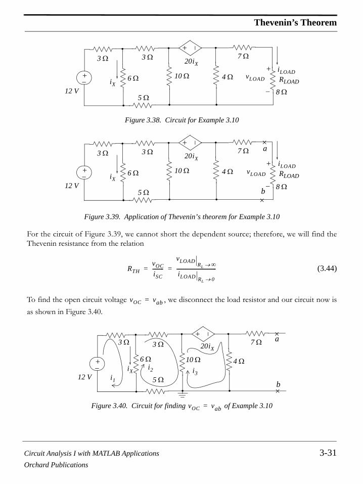
Circuit Analysis I with MATLAB Applications 3-31Orchard Publications
Thevenin’s Theorem
Figure 3.38. Circuit for Example 3.10
Figure 3.39. Application of Thevenin’s theorem for Example 3.10
For the circuit of Figure 3.39, we cannot short the dependent source; therefore, we will find theThevenin resistance from the relation
(3.44)
To find the open circuit voltage , we disconnect the load resistor and our circuit now isas shown in Figure 3.40.
Figure 3.40. Circuit for finding of Example 3.10
+ −
12 V
+−+−
3 Ω 3 Ω
5 Ω
6 Ω 10 Ω
7 Ω
8 Ω
RLOAD
+
−
4 Ω vLOAD
iLOAD
iX
20iX
+ −12 V
+−+−
3 Ω 3 Ω
5 Ω
6 Ω 10 Ω
7 Ω
8 Ω
RLOAD
+
−
4 Ω vLOAD
iLOAD
iX
20iX
×b
×a
RTHvOCiSC---------
vLOADRL ∞→
iLOAD RL 0→
--------------------------------= =
vOC vab=
+ −
12 V
+−+−
3 Ω 3 Ω
5 Ω
6 Ω 10 Ω
7 Ω
4 Ω
a×
b×
20iX
iXi1
i2 i3
vOC vab=

Chapter 3 Nodal and Mesh Equations - Circuit Theorems
3-32 Circuit Analysis I with MATLAB ApplicationsOrchard Publications
We will use mesh analysis to find which is the voltage across the resistor. We chose meshanalysis since we only need three mesh equations whereas we would need five equations had we cho-sen nodal analysis. Please refer to Exercise 16 at the end of this chapter for a solution requiring nodalanalysis.
Observing that , we write the three mesh equations for this network as
(3.45)
and after simplification and combination of like terms, we write them in matrix form as
(3.46)
Using the spreadsheet of Figure 3.41, we find that
Figure 3.41. Spreadsheet for Example 3.10
Thus, the Thevenin voltage at points a and b is
Next, to find the Thevenin resistance , we must first compute the short circuit current .Accordingly, we place a short across points a and b and the circuit now is as shown in Figure 3.42and we can find the short circuit current from the circuit of Figure 3.43 where
vOC 4 Ω
iX i1 i2–=
9i1 6i2– 12=
6i1– 24i2 10i3–+ 0=
20 i1 i2–( ) 4i3 10 i3 i2–( )+ + 0=
3 2– 03 12– 5
10 15– 7
R
I1
I2
I3
I
400
V
=
⎧ ⎪ ⎪ ⎨ ⎪ ⎪ ⎩ ⎧ ⎨ ⎩ ⎧ ⎨ ⎩i3 3.53 A–=
123456789
A B C D E F G HSpreadsheet for Matrix Inversion and Matrix Multiplication
3 -2 0 4R= 3 -12 5 V= 0
10 -15 7 0
0.106 -0.165 0.118 0.42R-1= -0.341 -0.247 0.176 I= -1.36
-0.882 -0.294 0.353 -3.53
vTH 3.53–( ) 4× 14.18 V–= =
RTH ISC
iSC iSC i4=

Circuit Analysis I with MATLAB Applications 3-33Orchard Publications
Thevenin’s Theorem
Figure 3.42. Circuit for finding in Example 3.10
Figure 3.43. Mesh equations for finding in Example 3.10
The mesh equations for the circuit of Figure 3.43 are
(3.47)
and after simplification and combination of like terms, we write them in matrix form as
(3.48)
We will solve these using MATLAB as follows:
+ −
12 V
+−+−
3 Ω 3 Ω
5 Ω
6 Ω 10 Ω
7 Ω
4 Ω
a×
b×
iX
iSC
20iX
iSC iab=
+ −12 V
+−+−
3 Ω 3 Ω
5 Ω
6 Ω 10 Ω
7 Ω
4 Ω
a×
b×
iX
iSC
20iX
i1
i2 i3i4
iSC iab=
9i1 6i2– 12=
6i1– 24i2 10i3–+ 0=
20 i1 i2–( ) 4 i3 i4–( ) 10 i3 i2–( )+ + 0=
4i3– 11i4+ 0=
3 2– 0 03 12– 5 0
10 15– 7 2–
0 0 4– 11
R
i1
i2
i3
i4
I
4000
V
=
⎧ ⎪ ⎪ ⎨ ⎪ ⎪ ⎩ ⎧ ⎨ ⎩ ⎧ ⎨ ⎩

Chapter 3 Nodal and Mesh Equations - Circuit Theorems
3-34 Circuit Analysis I with MATLAB ApplicationsOrchard Publications
R=[3 −2 0 0; 3 −12 5 0; 10 −15 7 −2; 0 0 −4 11]; V=[4 0 0 0]'; I=R\V;fprintf(' \n');...fprintf('i1 = %3.4f A \t',I(1,1)); fprintf('i2 = %3.4f A \t',I(2,1));...fprintf('i3 = %3.4f A \t',I(3,1)); fprintf('i4 = %3.4f A \t',I(4,1));...fprintf(' \n');...fprintf(' \n')
i1 = 0.0173 A i2 = -1.9741 A i3 = -4.7482 A i4 = -1.7266 A
Therefore,
and
The Thevenin equivalent is as shown in Figure 3.44.
Figure 3.44. Final form of Thevenin’s equivalent for the circuit of Example 3.10
Finally, with the load RLOAD attached to points a and b, the circuit is as shown in Figure 3.45.
Figure 3.45. Circuit for finding and in Example 3.10
Therefore, using the voltage division expression and Ohm’s law we get
iSC i4 1.727–= =
RTHvOCiSC--------- 14.18–
1.727–---------------- 8.2 Ω= = =
vTH
+−+−
RTH
8.2 Ω
−14.18 V
×a
×b
vTH
+−+−
RTH
8.2 Ω
−14.18 V 8 Ω
×
RLOAD
a
+
−
×b
vLOAD
iLOAD
vLOAD iLOAD

Circuit Analysis I with MATLAB Applications 3-35Orchard Publications
Norton’s Theorem
3.6 Norton’s Theorem
This theorem is analogous to Thevenin’s theorem and states that we can replace everything, exceptthe load, in a circuit by an equivalent circuit containing only an independent current source whichwe will denote as in parallel with a resistance which we will denote as , as shown in Figure3.46.
Figure 3.46. Replacement of a network by its Norton equivalent
The current source has the value of the short circuit current which would flow if a short wereconnected between the terminals x and y, where the Norton equivalent is inserted, and the resis-tance is found from the relation
(3.49)
where is the open circuit voltage which appears across the open terminals x and y.
Like Thevenin’s, Norton’s theorem is most useful when a series of computations involves changingthe load of a network while the rest of the circuit remains unchanged.
Comparing the Thevenin’s and Norton’s equivalent circuits, we see that one can be derived from theother by replacing the Thevenin voltage and its series resistance with the Norton current source andits parallel resistance. Therefore, there is no need to perform separate computations for each ofthese equivalents; once we know Thevenin’s equivalent we can easily draw the Norton equivalentand vice versa.
vLOAD8
8.2 8+----------------- 14.18–( )× 7.00 V–= =
iLOAD14.18–
8.2 8+----------------- 0.875 A–= =
iN RN
+−
Network to be replacedby a Nortonequivalent
circuit
x
y×
××
×
circuit)
(Rest of the
y
x
(a) (b)
Load Load
circuit)
(Rest of the
vxyvxyRNiN
iN
RN
RNvOCiSC---------=
vOC
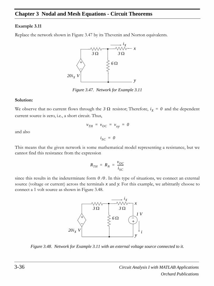
Chapter 3 Nodal and Mesh Equations - Circuit Theorems
3-36 Circuit Analysis I with MATLAB ApplicationsOrchard Publications
Example 3.11
Replace the network shown in Figure 3.47 by its Thevenin and Norton equivalents.
Figure 3.47. Network for Example 3.11
Solution:
We observe that no current flows through the resistor; Therefore, and the dependentcurrent source is zero, i.e., a short circuit. Thus,
and also
This means that the given network is some mathematical model representing a resistance, but wecannot find this resistance from the expression
since this results in the indeterminate form . In this type of situations, we connect an externalsource (voltage or current) across the terminals x and y. For this example, we arbitrarily choose toconnect a 1 volt source as shown in Figure 3.48.
Figure 3.48. Network for Example 3.11 with an external voltage source connected to it.
+−
3 Ω 3 Ω
6 Ω
x
y
iX
20iX V
3 Ω iX 0=
vTH vOC vxy 0= = =
iSC 0=
RTH RNvOCiSC
---------= =
0 0⁄
+−
3 Ω 3 Ω
6 Ω
x
y
+−+−
1 V
iX
20iX V i

Circuit Analysis I with MATLAB Applications 3-37Orchard Publications
Norton’s Theorem
In the circuit of Figure 3.48, the source represents the open circuit voltage and the currenti represents the short circuit current . Therefore, the Thevenin (or Norton) resistance will befound from the expression
(3.50)
Now, we can find i from the circuit of Figure 3.49 by application of KCL at Node .
Figure 3.49. Circuit for finding in Example 3.11
(3.51)
where
(3.52)
Simultaneous solution of (3.51) and (3.52) yields and . Then, from (3.50),
and the Thevenin and Norton equivalents are shown in Figure 3.50.
Figure 3.50. Thevenin’s and Norton’s equivalents for Example 3.11
1 V vOC
iSC
RTH RNvOCiSC--------- 1 V
i-------- 1 V
iX--------= = = =
+−
3 Ω 3 Ω
6 Ω
x
y
+−+−
1 V
iX
20iX V i
v1
iX
v1 20iX–
3----------------------
v16----- iX+ + 0=
iXv1 1–
3--------------=
v1 34 25⁄= iX 3 25⁄=
RTH RN1
3 25⁄------------- 25
3------= = =
25/3 Ω25/3 ΩvTH 0= iN 0=
RTH
RN

Chapter 3 Nodal and Mesh Equations - Circuit Theorems
3-38 Circuit Analysis I with MATLAB ApplicationsOrchard Publications
3.7 Maximum Power Transfer Theorem
Consider the circuit shown in Figure 3.51. We want to find the value of which will absorbmaximum power from the voltage source whose internal resistance is .
Figure 3.51. Circuit for computation of maximum power delivered to the load
The power delivered to the load is found from
or
(3.53)
To find the value of which will make maximum, we differentiate (3.53) with respect to. Recalling that
and differentiating (3.53), we get
(3.54)
and (3.54) will be zero if the numerator is set equal to zero, that is,
or
or
RLOAD
vS RS
+−+−
+
−vS
RS
RLOADvLOAD
iLOAD
RLOAD
pLOAD
pLOAD vLOAD iLOAD×RLOAD
RS RLOAD+-----------------------------vS⎝ ⎠
⎛ ⎞ vSRS RLOAD+-----------------------------⎝ ⎠
⎛ ⎞= =
pLOADRLOAD
RS RLOAD+( )2------------------------------------vS
2=
RLOAD pLOAD
RLOAD
xdd u
v---⎝ ⎠
⎛ ⎞v
xdd u( ) u
xdd v( )–
v2----------------------------------------=
RLOADd
dpLOAD RS RLOAD+( )2vS2 vS
2RLOAD 2( ) RS RLOAD+( )–
RS RLOAD+( )4-----------------------------------------------------------------------------------------------------------------=
RS RLOAD+( )2vS2 vS
2RLOAD 2( ) RS RLOAD+( )– 0=
RS RLOAD+ 2RLOAD=

Circuit Analysis I with MATLAB Applications 3-39Orchard Publications
Linearity
(3.55)
Therefore, we conclude that a voltage source with internal series resistance or a current sourcewith internal parallel resistance delivers maximum power to a load when or
. For example, in the circuits of 3.52, the voltage source and current source
deliver maximum power to the adjustable* load when
Figure 3.52. Circuits where is set to receive maximum power
We can use Excel or MATLAB to see that the load receives maximum power when it is set to thesame value as that of the resistance of the source. Figure 3.53 shows a spreadsheet with various val-ues of an adjustable resistive load. We observe that the power is maximum when .
The condition of maximum power transfer is also referred to as resistance matching or impedance match-ing. We will define the term “impedance” in Chapter 6.
The maximum power transfer theorem is of great importance in electronics and communicationsapplications where it is desirable to receive maximum power from a given circuit and efficiency isnot an important consideration. On the other hand, in power systems, this application is of no usesince the intent is to supply a large amount of power to a given load by making the internal resis-tance as small as possible.
3.8 Linearity
A linear passive element is one in which there is a linear voltage-current relationship such as
(3.56)
* An adjustable resistor is usually denoted with an arrow as shown in Figure 3.52.
RLOAD RS=
RS
RP RLOAD RLOAD RS=
RLOAD RP= vS iN
RLOAD RS RP 5 Ω= = =
+−+−
5 Ω
5 Ω +−
5 Ω
5 Ω
vS iS
RS
RNRLOADRLOAD
RLOAD
RLOAD 5 Ω=
RS
vR RiR= vL L tdd iL= iC C td
d vC=

Chapter 3 Nodal and Mesh Equations - Circuit Theorems
3-40 Circuit Analysis I with MATLAB ApplicationsOrchard Publications
Figure 3.53. Spreadsheet to illustrate maximum power transfer to a resistive load
Definition 3.1
A linear dependent source is a dependent voltage or current source whose output voltage or current isproportional only to the first power of some voltage or current variable in the circuit or a linear com-bination (the sum or difference of such variables). For example, is a linear relation-
ship but and are non-linear.
Definition 3.2
A linear circuit is a circuit which is composed entirely of independent sources, linear dependentsources and linear passive elements or a combination of these.
RLOAD PLOAD
0 0.001 2.782 4.083 4.694 4.945 5.006 4.967 4.868 4.739 4.59
10 4.4411 4.3012 4.1513 4.0114 3.8815 3.7516 3.63
Maximum Power Transfer
0
1
2
3
4
5
6
0 5 10 15 20
Resistance (Ohms) - Linear Scale
Pow
er (W
atts
)
Maximum Power Transfer
0123456
1 10 100
Resistance (Ohms) - Log Scale
Pow
er (W
atts
)
vxy 2v1 3i2–=
p vi Ri 2 v2 R⁄= = = i ISev nVT⁄
=
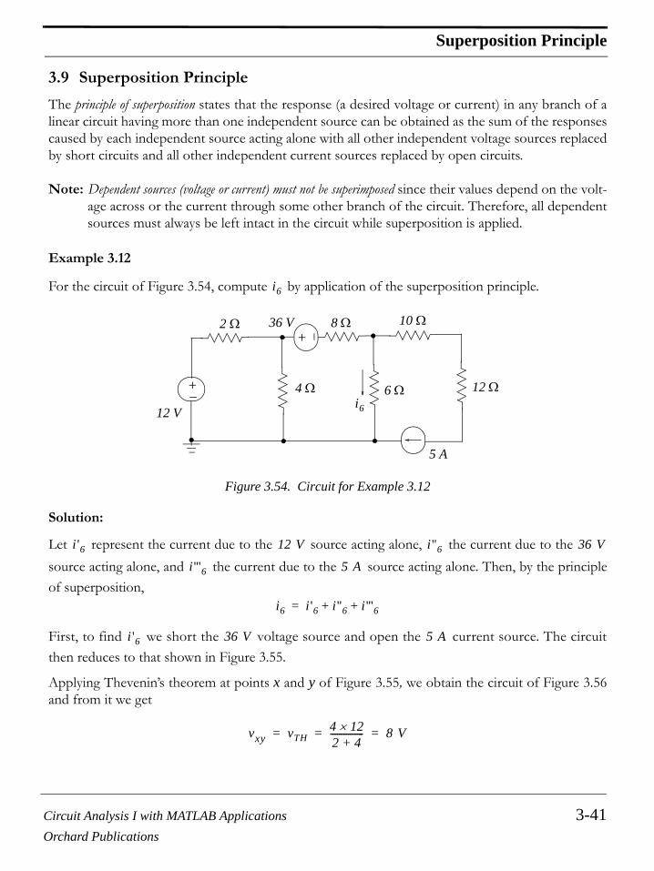
Circuit Analysis I with MATLAB Applications 3-41Orchard Publications
Superposition Principle
3.9 Superposition Principle
The principle of superposition states that the response (a desired voltage or current) in any branch of alinear circuit having more than one independent source can be obtained as the sum of the responsescaused by each independent source acting alone with all other independent voltage sources replacedby short circuits and all other independent current sources replaced by open circuits.
Note: Dependent sources (voltage or current) must not be superimposed since their values depend on the volt-age across or the current through some other branch of the circuit. Therefore, all dependentsources must always be left intact in the circuit while superposition is applied.
Example 3.12
For the circuit of Figure 3.54, compute by application of the superposition principle.
Figure 3.54. Circuit for Example 3.12
Solution:
Let represent the current due to the source acting alone, the current due to the source acting alone, and the current due to the source acting alone. Then, by the principleof superposition,
First, to find we short the voltage source and open the current source. The circuitthen reduces to that shown in Figure 3.55.
Applying Thevenin’s theorem at points x and y of Figure 3.55, we obtain the circuit of Figure 3.56and from it we get
i6
12 V
36 V 8 Ω
+−+−
+ −2 Ω 10 Ω
4 Ω 6 Ω 12 Ω
5 A
i6
i '6 12 V i ''6 36 V
i '''6 5 A
i6 i '6 i ''6 i '''6+ +=
i '6 36 V 5 A
vxy vTH4 12×2 4+--------------- 8 V= = =

Chapter 3 Nodal and Mesh Equations - Circuit Theorems
3-42 Circuit Analysis I with MATLAB ApplicationsOrchard Publications
Figure 3.55. Circuit for finding in Example 3.12
Figure 3.56. Circuit for computing the Thevenin voltage to find in Example 3.12
Next, we will use the circuit of Figure 3.57 to find the Thevenin resistance.
Figure 3.57. Circuit for computing the Thevenin resistance to find in Example 3.12
We find the current from Figure 3.58.
12 V
8 Ω
+−+−
2 Ω 10 Ω
4 Ω 6 Ω 12 Ω
x×
×y
i'6
i '6
12 V
8 Ω
+−+−
2 Ω
4 Ω
×
×x
y
i '6
y
8 Ω2 Ω
4 Ω
×
×x
RTH
i '6
RTH 8 4 2×4 2+-------------+
283
------ Ω= =
i '6

Circuit Analysis I with MATLAB Applications 3-43Orchard Publications
Superposition Principle
Figure 3.58. Circuit for computing in Example 3.12
(3.57)
Next, the current due to the source acting alone is found from the circuit of Figure 3.59.
Figure 3.59. Circuit for finding in Example 3.12
and after combination of the and parallel resistors to a single resistor, the circuit simplifiesto that shown in Figure 3.60.
Figure 3.60. Simplification of the circuit of Figure 3.59 to compute for Example 3.12
8 V
+−+−
10 Ω
6 Ω 12 Ω
vTH
RTH
i '6
i '6
i '68
28 3⁄ 6+----------------------- 12
23------ A= =
i ''6 36 V
36 V 8 Ω
+ −
2 Ω 10 Ω
4 Ω 6 Ω 12 Ω
i ''6
i ''6
2 Ω 4 Ω
36 V 8 Ω
+ −
10 Ω
6 Ω12 Ω
+
−i ''6
43--- Ω
i ''6

Chapter 3 Nodal and Mesh Equations - Circuit Theorems
3-44 Circuit Analysis I with MATLAB ApplicationsOrchard Publications
From the circuit of Figure 3.60, we get
(3.58)
Finally, to find , we short the voltage sources, and with the current source acting alone thecircuit reduces to that shown in Figure 3.61.
Figure 3.61. Circuit for finding in Example 3.12
Replacing the , , and resistors by a single resistor, we get
and the circuit of Figure 3.61 reduces to that shown in Figure 3.62.
Figure 3.62. Simplification of the circuit of Figure 3.59 to compute for Example 3.12
We will use the current division expression in the circuit of Figure 3.62 to find . Thus,
(3.59)
Therefore, from (3.57), (3.58), and (3.59) we get
i ''636
4 3⁄ 8 6+ +------------------------------–
5423------ A–= =
i '''6 5 A
8 Ω2 Ω 10 Ω
4 Ω 6 Ω 12 Ω
5 A
i '''6
i '''6
2 Ω 4 Ω 8 Ω
2 4×2 4+------------- 8+
283
------ Ω=
5 A
10 Ω
6 Ω 12 Ω283
------ Ω
i '''6
i '''6
i '''6
i '''628 3⁄
28 3⁄ 6+----------------------- 5–( )× 70
23------–= =
Circuit Analysis I with MATLAB Applications 3-45Orchard Publications
Circuits with Non-Linear Devices
or
(3.60)
and this is the same value as that of Example 3.5.
3.10 Circuits with Non-Linear Devices
Most electronic circuits contain non-linear devices such as diodes and transistors whose i - v (cur-rent-voltage) relationships are non-linear. However, for small signals (voltages or currents) these cir-cuits can be represented by linear equivalent circuit models. A detailed discussion of these is beyondthe scope of this text; however we will see how operational amplifiers can be represented by equiva-lent linear circuits in the next chapter.
If a circuit contains only one non-linear device, such as a diode, and all the other devices are linear,we can apply Thevenin’s theorem to reduce the circuit to a Thevenin equivalent in series with thenon-linear element. Then, we can analyze the circuit using a graphical solution. The procedure isillustrated with the following example.
Example 3.13
For the circuit of Figure 3.63, the characteristics of the diode are shown in figure 3.64. Wewish to find the voltage across the diode and the current through this diode using a graphicalsolution.
Figure 3.63. Circuit for Example 3.13
Solution:
The current through the diode is also the current through the resistor. Then, by KVL
i6 i '6 i ''6 i '''6+ + 1223------ 54
23------ 70
23------––
11223
--------- –= = =
i6 4.87 A–=
i v– DvD iD
1 V
+−+−
vTH
RTH
Diode; conducts currentonly in the indicated direction
vD
iD
D
1 KΩ
iD

Chapter 3 Nodal and Mesh Equations - Circuit Theorems
3-46 Circuit Analysis I with MATLAB ApplicationsOrchard Publications
Figure 3.64. Diode i-v characteristics
or
or
(3.61)
We observe that (3.61) is an equation of a straight line and the two points are obtained from it by firstletting , then, . We obtain the straight line shown in Figure 3.65 which is plotted onthe same graph as the given diode characteristics.
The intersection of the non-linear curve and the straight line yields the voltage and the current of thediode where we find that and .
Check:Since this is a series circuit, also. Therefore, the voltage drop across the resistor is
. Then, by KVL
0.00.20.40.60.81.01.21.4
0.0 0.1 0.2 0.3 0.4 0.5 0.6 0.7 0.8 0.9 1.0
vD (volts)
i D (m
illiam
ps)
vR vD+ 1 V=
RiD vD– 1+=
iD1R---vD– 1
R---+=
vD 0= iD 0=
i v–
vD 0.665V = iD 0.335 mA=
iR 0.335 mA= vR
vR 1 kΩ 0.335 mA× 0.335 V= =
vR vD+ 0.335 0.665+ 1 V= =

Circuit Analysis I with MATLAB Applications 3-47Orchard Publications
Efficiency
Figure 3.65. Curves for determining voltage and current in a diode
3.11 Efficiency
We have learned that the power absorbed by a resistor can be found from and this poweris transformed into heat. In a long length of a conductive material, such as copper, this lost power isknown as loss and thus the energy received by the load is equal to the energy transmitted minus
the loss. Accordingly, we define efficiency as
The efficiency is normally expressed as a percentage. Thus,
(3.62)
Obviously, a good efficiency should be close to
Example 3.14
In a two-story industrial building, the total load on the first floor draws an average of 60 amperesduring peak activity, while the total load of the second floor draws 40 amperes at the same time. Thebuilding receives its electric power from a source. Assuming that the total resistance of the
Diode Voltage Diode Current(Volts) (milliamps)
0.00 0.0000.02 0.0000.04 0.0000.06 0.0000.08 0.0000.10 0.0000.12 0.0000.14 0.0000.16 0.0000.18 0.0000.20 0.0000.22 0.0000.24 0.0000.26 0.0000.28 0.0000.30 0.000
I-V Relationship for Circuit of Example 3.13
0.00.20.40.60.81.01.21.4
0.0 0.1 0.2 0.3 0.4 0.5 0.6 0.7 0.8 0.9 1.0VD (volts)
I D (m
illia
mps
)
ID=−(1/R)VD+1/RDiode
pR i 2R=
i 2R
i 2R η
Efficiency η OutputInput
------------------ OutputOutput Loss+-------------------------------------= = =
η
% Efficiency % η OutputInput
------------------ 100× OutputOutput Loss+------------------------------------- 100×= = =
100%
480 V

Chapter 3 Nodal and Mesh Equations - Circuit Theorems
3-48 Circuit Analysis I with MATLAB ApplicationsOrchard Publications
cables (copper conductors) on the first floor is and on the second floor is , compute theefficiency of transmission.
Solution:
First, we draw a circuit that represents the electrical system of this building. This is shown in Figure3.66.
Figure 3.66. Circuit for Example 3.14
Power supplied by the source:
(3.63)
Power loss between source and 1st floor load:
(3.64)
Power loss between source and 2nd floor load:
(3.65)
Total power loss:
(3.66)
Total power received by 1st and 2nd floor loads:
(3.67)
(3.68)
1 Ω 1.6 Ω
480 V
0.8 Ω
+−+−
0.5 Ω
0.5 Ω
1st FloorLoad
60 A2nd Floor
Load
0.8 Ω
40 AvSi2i1
pS
pS vS i1 i2+( ) 480 60 40+( )× 48 kilowatts= = =
ploss1 i12 0.5 Ω 0.5 Ω+( ) 60 2 1× 3.6 kilowatts= = =
ploss2 i22 0.8 Ω 0.8 Ω+( ) 40 2 1.6× 2.56 kilowatts= = =
ploss ploss1 ploss2 + 3.60 2.56+ 6.16 kilowatts= = =
pL
pL pS ploss– 48.00 6.16– 41.84 kilowatts= = =
% Efficiency % η OutputInput
------------------ 100× 41.8448.00------------- 100× 87.17 %= = = =
Circuit Analysis I with MATLAB Applications 3-49Orchard Publications
Regulation
3.12 Regulation
The regulation is defined as the ratio of the change in load voltage when the load changes from noload (NL) to full load (FL) divided by the full load. Thus, denoting the no-load voltage as andthe full-load voltage as , the regulation is defined as In other words,
The regulation is also expressed as a percentage. Thus,
(3.69)
Example 3.15
Compute the regulation for the 1st floor load of the previous example.
Solution:
The current drawn by 1st floor load is given as 60 A and the total resistance from the source to theload as . Then, the total voltage drop in the conductors is . Therefore, the full-load voltage of the load is and the percent regulation is
3.13 Summary
• When using nodal analysis, for a circuit that contains nodes, we must write independentnodal equations in order to completely describe that circuit. When the presence of voltagesources in a circuit seem to complicate the nodal analysis because we do not know the currentthrough those voltage sources, we create combined nodes as illustrated in Example 3.2.
• When using nodal analysis, for a circuit that contains meshes or loops, branches, and nodes, we must write independent loop or mesh equations in order to com-pletely describe that circuit. When the presence of current sources in a circuit seem to complicatethe mesh or loop analysis because we do not know the voltage across those current sources, wecreate combined meshes as illustrated in Example 3.6.
vNL
vFL
RegulationvNL vFL–
vFL----------------------=
%RegulationvNL vFL–
vFL---------------------- 100×=
1 Ω 60 1× 60 V=
vFL 480 60– 420 V=( )=
% RegulationvNL vFL–
vFL---------------------- 100× 480 420–
420------------------------ 100× 14.3 %= = =
N N 1–
M L B NL M B N– 1+= =

Chapter 3 Nodal and Mesh Equations - Circuit Theorems
3-50 Circuit Analysis I with MATLAB ApplicationsOrchard Publications
• A practical voltage source has an internal resistance and it is represented by a voltage source whosevalue is the value of the ideal voltage source in series with a resistance whose value is the value ofthe internal resistance.
• A practical current source has an internal conductance and it is represented by a current sourcewhose value is the value of the ideal current source in parallel with a conductance whose value isthe value of the internal conductance.
• A practical voltage source in series with a resistance can be replaced by a current source whose value is in parallel with a resistance whose value is the same as
• A practical current source in parallel with a resistance can be replaced by a voltage source whose value is equal to in series with a resistance whose value is the same as
• Thevenin’s theorem states that in a two terminal network we can be replace everything except theload, by a voltage source denoted as in series with a resistance denoted as . The value of
represents the open circuit voltage where the circuit is isolated from the load and is theequivalent resistance of that part of the isolated circuit. If a given circuit contains independentvoltage and independent current sources only, the value of can be found by first shorting allindependent voltage sources, opening all independent current sources, and calculating the resis-tance looking into the direction which is opposite to the disconnected load. If the circuit containsdependent sources, the value of must be computed from the relation
• Norton’s theorem states that in a two terminal network we can be replace everything except theload, by a current source denoted as in parallel with a resistance denoted as . The value of
represents the short circuit current where the circuit is isolated from the load and is theequivalent resistance of that part of the isolated circuit. If the circuit contains independent voltageand independent current sources only, the value of can be found by first shorting all indepen-dent voltage sources, opening all independent current sources, and calculating the resistance look-ing into the direction which is opposite to the disconnected load. If the circuit contains dependentsources, the value of must be computed from the relation
• The maximum power transfer theorem states that a voltage source with a series resistance or acurrent source with parallel resistance delivers maximum power to a load when
or
• Linearity implies that there is a linear voltage−current relationship.
• A linear circuit is composed entirely of independent voltage sources, independent current sources,linear dependent sources, and linear passive devices such as resistors, inductors, and capacitors.
vS RS iS
vS iS⁄ RP RS
iS RP
vS iS RS× RS RP
vTH RTH
vTH RTH
RTH
RTH RTH vOC iSC⁄=
iN RN
iN RN
RN
RN RN vOC iSC⁄=
RS
RS RLOAD
RLOAD RS= RLOAD RN=

Circuit Analysis I with MATLAB Applications 3-51Orchard Publications
Summary
• The principle of superposition states that the response (a desired voltage or current) in anybranch of a linear circuit having more than one independent source can be obtained as the sumof the responses caused by each independent source acting alone with all other independent volt-age sources replaced by short circuits and all other independent current sources replaced by opencircuits.
• Efficiency is defined as the ratio of output to input and thus it is never greater than unity. It isnormally expressed as a percentage.
• Regulation is defined as the ratio of to and ideally should be close to zero. It isnormally expressed as a percentage.
.
vNL vFL– vFL

Chapter 3 Nodal and Mesh Equations - Circuit Theorems
3-52 Circuit Analysis I with MATLAB ApplicationsOrchard Publications
3.14 Exercises
Multiple Choice
1. The voltage across the resistor in the circuit of Figure 3.67 is
A.
B.
C.
D.
E.
Figure 3.67. Circuit for Question 1
2. The current in the circuit of Figure 3.68 is
A.
B.
C.
D.
E.
Figure 3.68. Circuit for Question 2
2 Ω
6 V
16 V
8– V
32 V
none of the above
8 A
6 V
+−
+−2 Ω
8 A
i
2– A
5 A
3 A
4 A
none of the above
+−
2 Ω
+ −
2 Ω
2 Ω2 Ω
4 V
10 V i

Circuit Analysis I with MATLAB Applications 3-53Orchard Publications
Exercises
3. The node voltages shown in the partial network of Figure 3.69 are relative to some referencenode which is not shown. The current is
A.
B.
C.
D.
E.
Figure 3.69. Circuit for Question 3
4. The value of the current for the circuit of Figure 3.70 is
A.
B.
C.
D.
E.
Figure 3.70. Circuit for Question 4
i
4– A
8 3⁄ A
5– A
6– A
none of the above
+−
2 Ω
+ −
2 Ω
2 Ω
8 V4 V
i
+ −8 V
8 V
13 V6 V
6 V
12 V
i
3– A
8– A
9– A
6 A
none of the above
+−
6 Ω
3 Ω8 A12 V 6 Ω
3 Ωi

Chapter 3 Nodal and Mesh Equations - Circuit Theorems
3-54 Circuit Analysis I with MATLAB ApplicationsOrchard Publications
5. The value of the voltage for the circuit of Figure 3.71 is
A.
B.
C.
D.
E.
Figure 3.71. Circuit for Question 5
6. For the circuit of Figure 3.72, the value of is dimensionless. For that circuit, no solution is pos-sible if the value of is
A.
B.
C.
D.
E.
Figure 3.72. Circuit for Question 6
v
4 V
6 V
8 V
12 V
none of the above
2 A 2 Ω
2 Ω
+
+ −
−
+
−
v
vX
2vX
kk
2
1
∞
0
none of the above
2 A 4 Ω
4 Ω
+−
+
−
v kv

Circuit Analysis I with MATLAB Applications 3-55Orchard Publications
Exercises
7. For the network of Figure 3.73, the Thevenin equivalent resistance to the right of terminalsa and b is
A.
B.
C.
D.
E.
Figure 3.73. Network for Question 7
8. For the network of Figure 3.74, the Thevenin equivalent voltage across terminals a and b is
A.
B.
C.
D.
E.
Figure 3.74. Network for Question 8
RTH
1
2
5
10
none of the above
2 Ω
3 Ω
a
b
RTH
2 Ω
2 Ω 2 Ω
2 Ω
4 Ω
VTH
3 V–
2 V–
1 V
5 V
none of the above
+ −
2 Ω 2 A2 V
2 Ω
a
b

Chapter 3 Nodal and Mesh Equations - Circuit Theorems
3-56 Circuit Analysis I with MATLAB ApplicationsOrchard Publications
9. For the network of Figure 3.75, the Norton equivalent current source and equivalent parallelresistance across terminals a and b are
A.
B.
C.
D.
E.
Figure 3.75. Network for Question 9
10. In applying the superposition principle to the circuit of Figure 3.76, the current due to the source acting alone is
A.
B.
C.
D.
E.
Figure 3.76. Network for Question 10
IN
RN
1 A 2 Ω,
1.5 A 25 Ω,
4 A 2.5 Ω,
0 A 5Ω,
none of the above
2 A5 Ω
a
b
5 Ω
2 A
i 4 V
8 A
1– A
4 A
2– A
none of the above
8 A 2 Ω
2 Ω
4 V+−
i
2 Ω
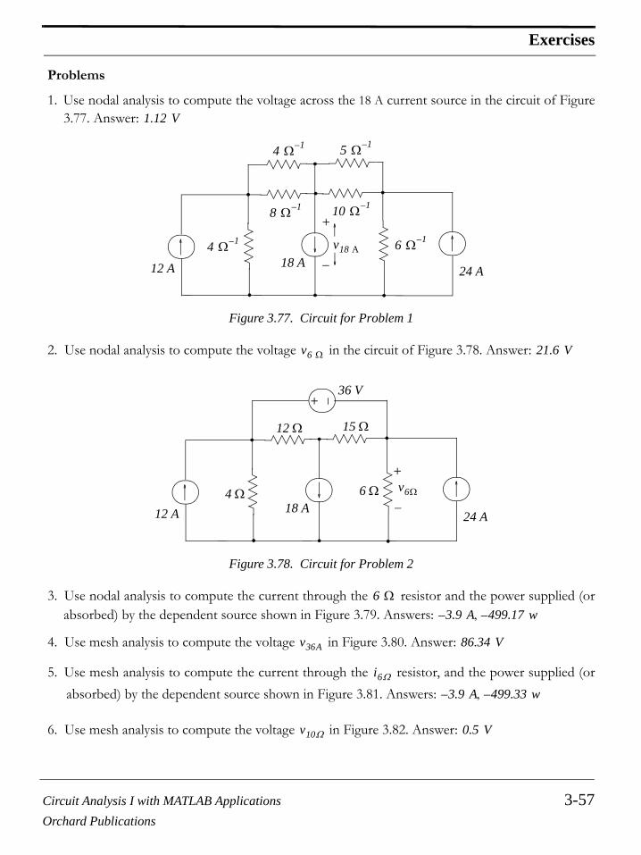
Circuit Analysis I with MATLAB Applications 3-57Orchard Publications
Exercises
Problems
1. Use nodal analysis to compute the voltage across the 18 A current source in the circuit of Figure3.77. Answer:
Figure 3.77. Circuit for Problem 1
2. Use nodal analysis to compute the voltage in the circuit of Figure 3.78. Answer:
Figure 3.78. Circuit for Problem 2
3. Use nodal analysis to compute the current through the resistor and the power supplied (orabsorbed) by the dependent source shown in Figure 3.79. Answers:
4. Use mesh analysis to compute the voltage in Figure 3.80. Answer:
5. Use mesh analysis to compute the current through the resistor, and the power supplied (orabsorbed) by the dependent source shown in Figure 3.81. Answers:
6. Use mesh analysis to compute the voltage in Figure 3.82. Answer:
1.12 V
12 A 24 A18 A
+
−
10 Ω 1–
4 Ω 1– 6 Ω 1–
8 Ω 1–
4 Ω 1– 5 Ω 1–
v18 A
v6 Ω 21.6 V
12 A 24 A18 A
4 Ω 6 Ω
12 Ω 15 Ω
+
−
+ −
36 V
v6Ω
6 Ω3.9 A 499.17 w–,–
v36A 86.34 V
i6Ω
3.9 A 499.33 w–,–
v10Ω 0.5 V

Chapter 3 Nodal and Mesh Equations - Circuit Theorems
3-58 Circuit Analysis I with MATLAB ApplicationsOrchard Publications
Figure 3.79. Circuit for Problem 3
Figure 3.80. Circuit for Problem 4
Figure 3.81. Circuit for Problem 5
12 A 24 A
4 Ω6 Ω
12 Ω 15 Ω
36 V
+
−
+−
iX
5iXi6Ω
18 A
12 A
240 V
36 A4 Ω
6 Ω
8 Ω 12 Ω+
−
+ −+
−120 V
24 A
4 Ω 3 Ω
v36A
12 A 24 A
18 A
4 Ω6 Ω
12 Ω 15 Ω
36 V
+
−
+−i6Ω
iX
5iX

Circuit Analysis I with MATLAB Applications 3-59Orchard Publications
Exercises
Figure 3.82. Circuit for Problem 6
7. Compute the power absorbed by the resistor in the circuit of Figure 3.83 using any method.Answer:
Figure 3.83. Circuit for Problem 7
8. Compute the power absorbed by the resistor in the circuit of Figure 3.84 using anymethod. Answer:
Figure 3.84. Circuit for Problem 8
9. In the circuit of Figure 3.85:
a. To what value should the load resistor should be adjusted to so that it will absorbmaximum power? Answer:
12 V
4 Ω
6 Ω
12 Ω 15 Ω
+
−+
− +
−
24 V
10 Ω
8 Ω v10ΩiX
10iX
10 Ω1.32 w
12 V
6 Ω
2 Ω
+
−
+
−
24 V
10 Ω3 Ω
+
−36 V
20 Ω73.73 w
12 V
2 Ω
+ −
6 A
3 Ω
20 Ω
8 A
RLOAD
2.4 Ω

Chapter 3 Nodal and Mesh Equations - Circuit Theorems
3-60 Circuit Analysis I with MATLAB ApplicationsOrchard Publications
b. What would then the power absorbed by be? Answer:
Figure 3.85. Circuit for Problem 9
10. Replace the network shown in Figure 3.86 by its Norton equivalent.Answers:
Figure 3.86. Circuit for Problem 10
11. Use the superposition principle to compute the voltage in the circuit of Figure 3.87.Answer:
Figure 3.87. Circuit for Problem 11
RLOAD 135 w
12 A 18 A
4 Ω 6 Ω
12 Ω 15 Ω
+ −
36 V
RLOAD
iN 0 RN 23.75 Ω=,=
iX4 Ω 5 Ω
15 Ω
5iX
a
b
v18A
1.12 V
12 A 24 A18 A
+
−
10 Ω 1–
4 Ω 1– 6 Ω 1–
8 Ω 1–
4 Ω 1– 5 Ω 1–
v18 A
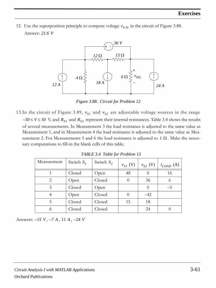
Circuit Analysis I with MATLAB Applications 3-61Orchard Publications
Exercises
12. Use the superposition principle to compute voltage in the circuit of Figure 3.88.Answer:
Figure 3.88. Circuit for Problem 12
13.In the circuit of Figure 3.89, and are adjustable voltage sources in the range V, and and represent their internal resistances. Table 3.4 shows the results
of several measurements. In Measurement 3 the load resistance is adjusted to the same value asMeasurement 1, and in Measurement 4 the load resistance is adjusted to the same value as Mea-surement 2. For Measurements 5 and 6 the load resistance is adjusted to . Make the neces-sary computations to fill-in the blank cells of this table.
Answers: , , ,
TABLE 3.4 Table for Problem 13
Measurement Switch Switch (V) (V) (A)
1 Closed Open 48 0 162 Open Closed 0 36 63 Closed Open 0 −54 Open Closed 0 −425 Closed Closed 15 186 Closed Closed 24 0
v6 Ω
21.6 V
12 A 24 A18 A
4 Ω 6 Ω
12 Ω 15 Ω
+
−
+ −
36 V
v6Ω
vS1 vS2
50 V 50≤ ≤– RS1 RS2
1 Ω
S1 S2 vS1 vS2 iLOAD
15 V– 7 A– 11 A 24 V–

Chapter 3 Nodal and Mesh Equations - Circuit Theorems
3-62 Circuit Analysis I with MATLAB ApplicationsOrchard Publications
Figure 3.89. Network for Problem 13
14. Compute the efficiency of the electrical system of Figure 3.90. Answer:
Figure 3.90. Electrical system for Problem 14
15. Compute the regulation for the 2st floor load of the electrical system of Figure 3.91.Answer:
Figure 3.91. Circuit for Problem 15
+
− +
−
+
−
1 Ω
1 Ω
ResistiveLoad
Adjustable
S2S1
vS2
vS1
RS2
RS1iLOAD
vLOAD
76.6%
480 V
0.8 Ω
+−+−
0.5 Ω
0.5 Ω
1st FloorLoad
100 A2nd Floor
Load
0.8 Ω
80 AvSi2i1
36.4%
480 V
0.8 Ω
+−+−
0.5 Ω
0.5 Ω
1st FloorLoad
100 A2nd Floor
Load
0.8 Ω
80 AVS i1i2
Circuit Analysis I with MATLAB Applications 3-63Orchard Publications
Exercises
16. Write a set of nodal equations and then use MATLAB to compute and for the cir-cuit of Example 3.10 which is repeated as Figure 3.92 for convenience.Answers:
Figure 3.92. Circuit for Problem 16
iLOAD vLOAD
0.96 A 7.68 V–,–
+ −
12 V
+−+−
3 Ω 3 Ω
5 Ω
6 Ω10 Ω
7 Ω
8 Ω
RL
+
−
4 ΩiLOAD
iX
20iX
vLOAD

Chapter 3 Nodal and Mesh Equations - Circuit Theorems
3-64 Circuit Analysis I with MATLAB ApplicationsOrchard Publications
3.15 Answers to Exercises
Multiple Choice
1. E The current entering Node A is equal to the current leaving that node. Therefore, there is nocurrent through the resistor and the voltage across it is zero.
2. C From the figure below, . Also, and . Then, a n d . T he r e fo r e ,
.
3. A From the figure below we observe that the node voltage at A is relative to the referencenode which is not shown. Therefore, the node voltage at B is relative to thesame reference node. The voltage across the resistor is and the direc-tion of current through the resistor is opposite to that shown since Node B is at a higherpotential than Node C. Thus
2 Ω
8 A
6 V
+−
+−
2 Ω
8 A
A
8 A 8 A
VAC 4 V= VAB VBC 2 V= = VAD 10 V=
VBD VAD VAB– 10 2– 8 V= = = VCD VBD VBC– 8 2– 6 V= = =
i 6 2⁄ 3 A= =
+−
2 Ω
+ −
2 Ω
2 Ω2 Ω
4 V
10 V i
A B C
D
6 V6 12+ 18 V=
VBC 18 6– 12 V= =
3 Ωi 12 3⁄– 4 A–= =
+−
3 Ω
+ −
2 Ω
2 Ω
8 V4 V
i
+ −
8 V
8 V
13 V6 V
6 V
12 V
A
BC

Circuit Analysis I with MATLAB Applications 3-65Orchard Publications
Answers to Exercises
4. E We assign node voltages at Nodes A and B as shown below.
At Node A
and at Node B
These simplify to
and
Multiplication of the last equation by 2 and addition with the first yields and thus.
5. E Application of KCL at Node A of the circuit below yields
or
Also by KVL
+−
6 Ω
3 Ω8 A12 V 6 Ω
3 Ωi
A B
VA 12–
6------------------
VA6
------VA VB–
3-------------------+ + 0=
VB VA–
3-------------------
VB3
------+ 8=
23---VA
13---VB– 2=
13---– VA
23---VB+ 8=
VB 18=
i 18 3⁄– 6 A–= =
2 A 2 Ω
2 Ω
+
+ −
−
+
−
v
vX
2vX
A
v2---
v 2vX–
2-----------------+ 2=
v vX– 2=

Chapter 3 Nodal and Mesh Equations - Circuit Theorems
3-66 Circuit Analysis I with MATLAB ApplicationsOrchard Publications
and by substitution
or
and thus
6. A Application of KCL at Node A of the circuit below yields
or
and this relation is meaningless if . Thus, this circuit has solutions only if .
7. B The two resistors on the right are in series and the two resistors on the left shown inthe figure below are in parallel.
Starting on the right side and proceeding to the left we get , , ,.
v vX 2vX+=
vX 2vX vX–+ 2=
vX 1=
v vX 2vX+ 1 2 1×+ 3 V= = =
2 A 4 Ω
4 Ω
+−
+
−
v kv
A
v4--- v kv–
4--------------+ 2=
14--- 2v kv–( ) 2=
k 2= k 2≠
2 Ω 2 Ω
2 Ω
3 Ω
a
b
RTH
2 Ω
2 Ω 2 Ω
2 Ω
4 Ω
2 2+ 4= 4 4|| 2= 2 2+ 4=
4 3 2 2||+( )|| 4 3 1+( )|| 4 4|| 2 Ω= = =

Circuit Analysis I with MATLAB Applications 3-67Orchard Publications
Answers to Exercises
8. A Replacing the current source and its parallel resistance with an equivalent voltage sourcein series with a resistance we get the network shown below.
By Ohm’s law,
and thus
9. D The Norton equivalent current source is found by placing a short across the terminals aand b. This short shorts out the resistor and thus the circuit reduces to the one shownbelow.
By KCL at Node A,
and thus
The Norton equivalent resistance is found by opening the current sources and looking tothe right of terminals a and b. When this is done, the circuit reduces to the one shown below.
2 Ω2 Ω
+ −
2 Ω
2 V
2 Ω
a
b
+−
4 V
i
i 4 2–2 2+------------ 0.5 A= =
vTH vab 2 0.5 4–( )+× 3 V–= = =
IN
5 Ω
2 A
a
b
5 Ω
2 A
ISC IN= A
IN 2+ 2=
IN 0=
RN

Chapter 3 Nodal and Mesh Equations - Circuit Theorems
3-68 Circuit Analysis I with MATLAB ApplicationsOrchard Publications
Therefore, and the Norton equivalent circuit consists of just a resistor.10. B With the source acting alone, the circuit is as shown below.
We observe that and thus the voltage drop across each of the resistors to theleft of the source is with the indicated polarities. Therefore,
Problems
1. We first replace the parallel conductances with their equivalents and the circuit simplifies to thatshown below.
Applying nodal analysis at Nodes 1, 2, and 3 we get:
Node 1:
Node 2:
5 Ω
a
b
5 Ω
RN 5 Ω= 5 Ω
4 V
2 Ω
2 Ω
4 V+−
i
2 Ω
A
B
++
−
−
vAB 4 V= 2 Ω
4 V 2 V
i 2– 2⁄ 1 A–= =
12 A 24 A18 A
+
−4 Ω 1– 6 Ω 1–
12 Ω 1–
v18 A
v1 v2 v3
1 2 3
15 Ω 1–
16v1 12v2– 12=
12– v1 27v2 15v3–+ 18–=

Circuit Analysis I with MATLAB Applications 3-69Orchard Publications
Answers to Exercises
Node 3:
Simplifying the above equations, we get:
Addition of the first two equations above and grouping with the third yields
For this problem we are only interested in . Therefore, we will use Cramer’s rule tosolve for . Thus,
and
2. Since we cannot write an expression for the current through the source, we form a com-bined node as shown on the circuit below.
At Node 1 (combined node):
and at Node 2,
15– v2 21v3+ 24=
4v1 3v2 – 3=
4– v1 9v2 5v3–+ 6–=
5– v2 7v3+ 8=
6v2 5v3– 3–=
5– v2 7v3+ 8=
v2 v18 A=
v2
v2D2∆
------= D23– 5–
8 721– 40+ 19= = = ∆ 6 5–
5– 742 25– 17= = =
v2 v18 A 19 17⁄ 1.12 V= = =
36 V
12 A 24 A18 A
4 Ω 6 Ω
12 Ω 15 Ω
+
−
+ −
36 V
v6Ω
1v1
v2
v3
2 3
v14-----
v1 v2–
12----------------
v3 v2–
15----------------
v36----- 12 24––+ + + 0=

Chapter 3 Nodal and Mesh Equations - Circuit Theorems
3-70 Circuit Analysis I with MATLAB ApplicationsOrchard Publications
Also,
Simplifying the above equations, we get:
Addition of the first two equations above and multiplication of the third by yields
and by adding the last two equations we get
or
Check with MATLAB:
format ratR=[1/3 −3/20 7/30; −1/12 3/20 −1/15; 1 0 −1];I=[36 −18 36]';V=R\I;fprintf('\n'); disp('v1='); disp(V(1)); disp('v2='); disp(V(2)); disp('v3='); disp(V(3))
v1= 288/5 v2= -392/5 v3= 108/5
3. We assign node voltages , , , and current as shown in the circuit below. Then,
v2 v1–
12----------------
v2 v3–
15----------------+ 18–=
v1 v3– 36=
13---v1
320------v2–
730------v3+ 36=
112------– v1
320------v2
115------v3–+ 18–=
v1 v3– 36=
1– 4⁄
14---v1
16---v3+ 18=
14---– v1
14---v3+ 9–=
512------v3 9=
v3 v6 Ω1085
--------- 21.6V= = =
v1 v2 v3 v4 iY

Circuit Analysis I with MATLAB Applications 3-71Orchard Publications
Answers to Exercises
and
Simplifying the last two equations above, we get
and
Next, we observe that , and . Then and by
substitution into the last equation above, we get
or
Thus, we have two equations with two unknowns, that is,
v14-----
v1 v2–
12---------------- 18 12–+ + 0=
v2 v1–
12----------------
v2 v3–
12----------------
v2 v4–
6----------------+ + 0=
12 A 24 A
4 Ω6 Ω
12 Ω 15 Ω
36 V+−
+−
iX
5iXi6Ω
18 Av1 v2 v3
v4
iY
13---v1
112------v2– 6–=
112------v1–
1960------v2
115------v3
16---v4––+ 0=
iXv1 v2–
12----------------= v3 5iX= v4 36 V= v3
512------ v1 v2–( )=
112------v1–
1960------v2
115------ 5
12------ v1 v2–( )× 1
6---36––+ 0=
19---v1–
3190------v2+ 6=
13---v1
112------v2– 6–=
19---v1–
3190------v2+ 6=

Chapter 3 Nodal and Mesh Equations - Circuit Theorems
3-72 Circuit Analysis I with MATLAB ApplicationsOrchard Publications
Multiplication of the first equation above by and addition with the second yields
or
We find from
Thus,
or
Now, we find from
Therefore, the node voltages of interest are:
The current through the resistor is
To compute the power supplied (or absorbed) by the dependent source, we must first find thecurrent . It is found by application of KCL at node voltage . Thus,
or
1 3⁄
1960------v2 4=
v2 240 19⁄=
v1
13---v1
112------v2– 6–=
13---v1
112------ 240
19---------×– 6–=
v1 282– 19⁄=
v3
v3512------ v1 v2–( ) 5
12------ 282–
19------------ 240
19---------–⎝ ⎠
⎛ ⎞ 43538---------–= = =
v1 282– 19 V⁄=
v2 240 19 V⁄=
v3 435– 38 V⁄=
v4 36 V=
6 Ω
i6 Ωv2 v4–
6---------------- 240 19⁄ 36–
6------------------------------- 74
19------– 3.9 A–= = = =
iY v3
iY 24– 18–v3 v2–
15----------------+ 0=

Circuit Analysis I with MATLAB Applications 3-73Orchard Publications
Answers to Exercises
and
that is, the dependent source supplies power to the circuit.
4. Since we cannot write an expression for the current source, we temporarily remove it andwe form a combined mesh for Meshes 2 and 3 as shown below.
Mesh 1:
Combined mesh (2 and 3):
or
We now re-insert the current source and we write the third equation as
Mesh 4:
Mesh 5:
or
iY 42 435– 38 240 19⁄–⁄15
-----------------------------------------------–=
42 915 38⁄15
-------------------+ 165738
------------==
p v3iY43538
---------–1657
38------------× 72379
145---------------– 499.17 w–= = = =
36 A
12 A
240 V
4 Ω6 Ω
8 Ω 12 Ω
+ −+
−120 V
24 A
4 Ω 3 Ω
i1 i2i3 i4
i5i6
i1 12=
4i1– 12i2 18i3 6i4– 8i5– 12i6–+ + 0=
2i1– 6i2 9i3 3i4– 4i5– 6i6–+ + 0=
36 A
i2 i3– 36=
i4 24–=
8– i2 12i5+ 120=

Chapter 3 Nodal and Mesh Equations - Circuit Theorems
3-74 Circuit Analysis I with MATLAB ApplicationsOrchard Publications
Mesh 6:
or
Thus, we have the following system of equations:
and in matrix form
We find the currents through with the following MATLAB code:
R=[1 0 0 0 0 0; −2 6 9 −3 −4 −6;... 0 1 −1 0 0 0; 0 0 0 1 0 0;... 0 −2 0 0 3 0; 0 0 −4 0 0 5];V=[12 0 36 −24 30 −80]';I=R\V;fprintf('\n');... fprintf('i1=%7.2f A \t', I(1));... fprintf('i2=%7.2f A \t', I(2));... fprintf('i3=%7.2f A \t', I(3));... fprintf('\n');...
2– i2 3i5+ 30=
12– i3 15i6+ 240–=
4– i3 5i6+ 80–=
i1 12=
2i1– 6i2 9i3 3i4– 4i5– 6i6–+ + 0=
i2 i3 – 36=
i4 24–=
2– i2 3i5 + 30=
4– i3 5i6+ 80–=
1 0 0 0 0 02– 6 9 3– 4– 6–
0 1 1– 0 0 00 0 0 1 0 00 2– 0 0 3 00 0 4– 0 0 5
R
i1
i2
i3
i4
i5
i6
I
⋅
120
3624–
3080–
V
=
⎧ ⎪ ⎪ ⎪ ⎪ ⎨ ⎪ ⎪ ⎪ ⎪ ⎩
⎧ ⎨ ⎩ ⎧ ⎨ ⎩
i1 i6

Circuit Analysis I with MATLAB Applications 3-75Orchard Publications
Answers to Exercises
fprintf('i4=%7.2f A \t', I(4));... fprintf('i5=%7.2f A \t', I(5));... fprintf('i6=%7.2f A \t', I(6));... fprintf('\n')
i1= 12.00 A i2= 6.27 A i3= -29.73 A i4= -24.00 A i5= 14.18 A i6= -39.79 A
Now, we can find the voltage by application of KVL around Mesh 3. Thus,
or
To verify that this value is correct, we apply KVL around Mesh 2. Thus, we must show that
By substitution of numerical values, we find that
5. This is the same circuit as that of Problem 3. We will show that we obtain the same answers usingmesh analysis.
We assign mesh currents as shown below.
v36 A
12 A
240 V
36 A4 Ω
6 Ω
8 Ω 12 Ω+
−
+ −+
−120 V
24 A
4 Ω 3 Ω
v36 A
i5
i3i2
i1
i6
i4
v36 A v12 Ω v6 Ω+ 12 29.73–( ) 39.79–( )–[ ]× 6 29.73–( ) 24.00( )–[ ]×+= =
v36 A 86.34 V=
v4 Ω v8 Ω v36 A+ + 0=
4 6.27 12–[ ]× 8 6.27 14.18–[ ]× 86.34+ + 0.14=

Chapter 3 Nodal and Mesh Equations - Circuit Theorems
3-76 Circuit Analysis I with MATLAB ApplicationsOrchard Publications
Mesh 1:
Mesh 2:
or
Mesh 3:
and since , the above reduces to
or
Mesh 4:
Mesh 5:
Grouping these five independent equations we get:
and in matrix form,
12 A 24 A
18 A
4 Ω6 Ω
12 Ω 15 Ω
36 V
+
−
+−i6Ω
iX
5iX
i5
i1 i2
i3 i4
i1 12=
4i1– 22i2 6i3– 12i5–+ 36–=
2i1– 11i2 3i3– 6i5–+ 18–=
6– i2 21i3 15i5– 5iX+ + 36=
iX i2 i5–=
6– i2 21i3 15i5– 5i2 5i5–+ + 36=
i2– 21i3 20i5–+ 36=
i4 24–=
i5 18=
i1 12=
2i1– 11i2 3i3– 6i5–+ 18–=
i2– 21i3 20i5–+ 36=
i4 24–=
i5 18=

Circuit Analysis I with MATLAB Applications 3-77Orchard Publications
Answers to Exercises
We find the currents through with the following MATLAB code:
R=[1 0 0 0 0 ; −2 11 −3 0 −6; 0 −1 21 0 −20; ... 0 0 0 1 0; 0 0 0 0 1];V=[12 −18 36 −24 18]';I=R\V;fprintf('\n');... fprintf('i1=%7.2f A \t', I(1));... fprintf('i2=%7.2f A \t', I(2));... fprintf('i3=%7.2f A \t', I(3));... fprintf('\n');... fprintf('i4=%7.2f A \t', I(4));... fprintf('i5=%7.2f A \t', I(5));... fprintf('\n')
i1= 12.00 A i2= 15.71 A i3= 19.61 A i4= -24.00 A i5= 18.00 A
By inspection,
Next,
These are the same answers as those we found in Problem 3.
6. We assign mesh currents as shown below and we write mesh equations.
1 0 0 0 02– 11 3– 0 6–
0 1– 21 0 20–
0 0 0 1 00 0 0 0 1
R
i1
i2
i3
i4
i5
I
⋅
1218–
3624–
18
V
=
⎧ ⎪ ⎪ ⎪ ⎨ ⎪ ⎪ ⎪ ⎩ ⎧ ⎨ ⎩ ⎧ ⎨ ⎩
i1 i5
i6 Ω i2 i3– 15.71 19.61– 3.9 A–= = =
p5iX5iX i3 i4–( ) 5 i2 i5–( ) i3 i4–( )= =
5 15.71 18.00–( ) 19.61 24.00+( ) 499.33 w–==

Chapter 3 Nodal and Mesh Equations - Circuit Theorems
3-78 Circuit Analysis I with MATLAB ApplicationsOrchard Publications
Mesh 1:
or
Mesh 2:
Mesh 3:
or
Mesh 4:
or
Grouping these four independent equations we get:
and in matrix form,
12 V
4 Ω
6 Ω
12 Ω 15 Ω
+
−+
− +
−
24 V
10 Ω
8 Ω v10ΩiX
10iX
i1i2 i3
i4
24i1 8i2– 12i4– 24 12–– 0=
6i1 2i2– 3i4– 9=
8– i1 29i2 6i3– 15i4–+ 24–=
6– i2 16i3+ 0=
3– i2 8i3+ 0=
i4 10iX 10 i2 i3–( )==
10i2 10i3– i4– 0=
6i1 2i2 – 3i4– 9=
8– i1 29i2 6i3– 15i4–+ 24–=
3– i2 8i3 + 0=
10i2 10i3– i4– 0=
6 2– 0 3–
8– 29 6– 15–
0 3– 8 00 10 10– 1–
R
i1
i2
i3
i4
I
⋅
924–
00
V
=
⎧ ⎪ ⎪ ⎪ ⎨ ⎪ ⎪ ⎪ ⎩ ⎧ ⎨ ⎩ ⎧ ⎨ ⎩

Circuit Analysis I with MATLAB Applications 3-79Orchard Publications
Answers to Exercises
We find the currents through with the following MATLAB code:
R=[6 −2 0 −3; −8 29 −6 −15; 0 −3 8 0 ; 0 10 −10 −1];V=[9 −24 0 0]';I=R\V;fprintf('\n');... fprintf('i1=%7.2f A \t', I(1));... fprintf('i2=%7.2f A \t', I(2));... fprintf('i3=%7.2f A \t', I(3));... fprintf('i4=%7.2f A \t', I(4));...
fprintf('\n')
i1= 1.94 A i2= 0.13 A i3= 0.05 A i4= 0.79 A
Now, we find by Ohm’s law, that is,
The same value is obtained by computing the voltage across the resistor, that is,
7. Voltage-to-current source transformation yields the circuit below.
By combining all current sources and all parallel resistors except the resistor, we obtain thesimplified circuit below.
Applying the current division expression, we get
and thus
i1 i4
v10Ω
v10Ω 10i3 10 0.05× 0.5 V= = =
6 Ω
v6Ω 6 i2 i3–( ) 6 0.13 0.05–( ) 0.48 V= = =
10 Ω2 Ω 3 Ω6 A 8 A 6 A
6 Ω
10 Ω
10 Ω1 Ω
4 A
i10 Ω1
1 10+--------------- 4× 4
11------ A= =
p10 Ω i10 Ω2 10( ) 4
11------⎝ ⎠
⎛ ⎞ 210× 16
121--------- 10× 160
121--------- 1.32 w= = = = =
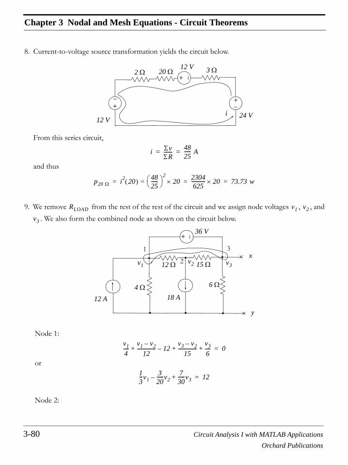
Chapter 3 Nodal and Mesh Equations - Circuit Theorems
3-80 Circuit Analysis I with MATLAB ApplicationsOrchard Publications
8. Current-to-voltage source transformation yields the circuit below.
From this series circuit,
and thus
9. We remove from the rest of the rest of the circuit and we assign node voltages , , and. We also form the combined node as shown on the circuit below.
Node 1:
or
Node 2:
12 V2 Ω
+ − 3 Ω20 Ω
+
−
12 V+
−
24 Vi
i ΣvΣR------- 48
25------ A= =
p20 Ω i2 20( ) 4825------⎝ ⎠
⎛ ⎞ 220×=
2304625
------------ 20× 73.73 w= = =
RLOAD v1 v2
v3
12 A 18 A
4 Ω 6 Ω
12 Ω 15 Ω
+ −
36 V
v1 v2 v3
x
y
×
×
1
2
3
v14-----
v1 v2–
12---------------- 12–
v3 v2–
15----------------
v36-----+ + + 0=
13---v1
320------v2–
730------v3+ 12=

Circuit Analysis I with MATLAB Applications 3-81Orchard Publications
Answers to Exercises
or
Also,
For this problem, we are interested only in the value of which is the Thevenin voltage ,and we could find it by Gauss’s elimination method. However, for convenience, we will groupthese three independent equations, express these in matrix form, and use MATLAB for theirsolution.
and in matrix form,
We find the voltages through with the following MATLAB code:
G=[1/3 −3/20 7/30; −1/12 3/20 −1/15; 1 0 −1];I=[12 −18 36]'; V=G\I;fprintf('\n');... fprintf('v1=%7.2f V \t', V(1)); fprintf('v2=%7.2f V \t', V(2)); fprintf('v3=%7.2f V \t', V(3)); fprintf('\n')
v1= 0.00 V v2= -136.00 V v3= -36.00 V
Thus,
v2 v1–
12----------------
v2 v3–
15----------------+ 18–=
112------– v1
320------v2
115------– v3+ 18–=
v1 v3– 36=
v3 vTH
13---v1
320------v2–
730------v3+ 12=
112------– v1
320------v2
115------– v3+ 18–=
v1 v3– 36=
13--- 3
20------–
730------
112------–
320------ 1
15------–
1 0 1–
G
v1
v2
v3
V
⋅
1218–
36
I
=
⎧ ⎪ ⎪ ⎨ ⎪ ⎪ ⎩
⎧ ⎨ ⎩ ⎧ ⎨ ⎩
v1 v3
vTH v3 36 V–= =

Chapter 3 Nodal and Mesh Equations - Circuit Theorems
3-82 Circuit Analysis I with MATLAB ApplicationsOrchard Publications
To find we short circuit the voltage source and we open the current sources. The circuit thenreduces to the resistive network below.
We observe that the resistors in series are shorted out and thus the Thevenin resistance is the par-allel combination of the and resistors, that is,
and the Thevenin equivalent circuit is as shown below.
Now, we connect the load resistor at the open terminals and we get the simple series cir-cuit shown below.
a. For maximum power transfer,
b. Power under maximum power transfer condition is
RTH
4 Ω 6 Ω
12 Ω 15 Ωx
y
×
×
RTH
4 Ω 6 Ω
4 Ω 6 Ω|| 2.4 Ω=
2.4 Ω
+
−
36 V
RLOAD
2.4 Ω
+
−
36 V
RLOAD 2.4 Ω=
RLOAD 2.4 Ω=

Circuit Analysis I with MATLAB Applications 3-83Orchard Publications
Answers to Exercises
10. We assign a node voltage Node 1 and a mesh current for the mesh on the right as shown below.
At Node 1:
Mesh on the right:
and by substitution into the node equation above,
or
but this can only be true if .
Then,
Thus, the Norton current source is open as shown below.
To find we insert a current source as shown below.
pMAX i2RLOAD36
2.4 2.4+---------------------⎝ ⎠
⎛ ⎞ 22.4× 7.52 2.4× 135 w= == =
iX4 Ω 5 Ω
15 Ω
5iX
a
b
1
v1 iX
iX
v14----- iX+ 5iX=
15 5+( )iX v1=
20iX4
---------- iX+ 5iX=
6iX 5iX=
iX 0=
iNvOCRN---------
vabRN-------
5 iX×RN
------------- 5 0×RN
------------ 0= = = = =
iX
a
b
RN
RN 1 A

Chapter 3 Nodal and Mesh Equations - Circuit Theorems
3-84 Circuit Analysis I with MATLAB ApplicationsOrchard Publications
At Node A:
But
and by substitution into the above relation
or
At Node B:
or
For this problem, we are interested only in the value of which we could find by Gauss’s elimi-nation method. However, for convenience, we will use MATLAB for their solution.
iX4 Ω 5 Ω
15 Ω
5iX
a
b
A
vA iX
iX 1 A
vB
B
vA4-----
vA vB–
15-----------------+ 5iX=
vB 5 Ω( ) iX× 5iX= =
vA4-----
vA vB–
15-----------------+ vB=
1960------vA
1615------vB– 0=
vB vA–
15-----------------
vB5-----+ 1=
115------vA–
415------vB+ 1=
vB
1960------vA
1615------vB– 0=
115------vA–
415------vB+ 1=

Circuit Analysis I with MATLAB Applications 3-85Orchard Publications
Answers to Exercises
and in matrix form,
We find the voltages and with the following MATLAB code:
G=[19/60 −16/15; −1/15 4/15];I=[0 1]'; V=G\I;fprintf('\n');... fprintf('vA=%7.2f V \t', V(1)); fprintf('vB=%7.2f V \t', V(2)); fprintf('\n')
vA= 80.00 V vB= 23.75 V
Now, we can find the Norton equivalent resistance from the relation
11. This is the same circuit as that of Problem 1. Let be the voltage due to the currentsource acting alone. The simplified circuit with assigned node voltages is shown below wherethe parallel conductances have been replaced by their equivalents.
The nodal equations at the three nodes are
or
1960------ 16
15------–
115------–
415------
G
vA
vB
V
⋅01
I
=
⎧ ⎪ ⎨ ⎪ ⎩
⎧ ⎨ ⎩ ⎧ ⎨ ⎩
v1 v2
RNVabISC--------
VB1
------ 23.75 Ω= = =
v'18A 12 A
12 A
+
−
15 Ω 1–
4 Ω 1– 6 Ω 1–
12 Ω 1–
v'18A
v1 v2 v3
16v1 12v2 – 12=
12v1– 27v2 15v3–+ 0=
15– v2 21v3+ 0=
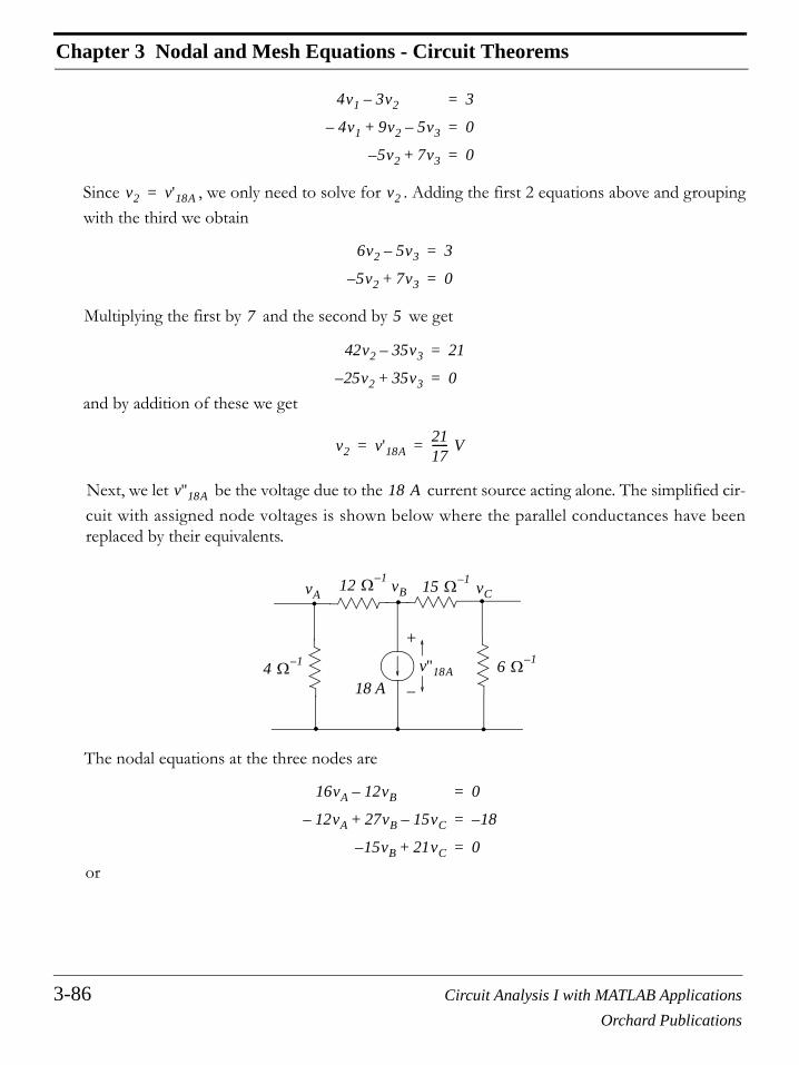
Chapter 3 Nodal and Mesh Equations - Circuit Theorems
3-86 Circuit Analysis I with MATLAB ApplicationsOrchard Publications
Since , we only need to solve for . Adding the first 2 equations above and groupingwith the third we obtain
Multiplying the first by and the second by we get
and by addition of these we get
Next, we let be the voltage due to the current source acting alone. The simplified cir-cuit with assigned node voltages is shown below where the parallel conductances have beenreplaced by their equivalents.
The nodal equations at the three nodes are
or
4v1 3v2 – 3=
4v1– 9v2 5v3–+ 0=
5– v2 7v3+ 0=
v2 v'18A= v2
6v2 5v3– 3=
5– v2 7v3+ 0=
7 5
42v2 35v3– 21=
25– v2 35v3+ 0=
v2 v'18A2117------ V= =
v''18A 18 A
18 A
+
−
15 Ω 1–
4 Ω 1– 6 Ω 1–
12 Ω 1–
v''18A
vA vB vC
16vA 12vB – 0=
12vA– 27vB 15vC–+ 18–=
15– vB 21vC+ 0=
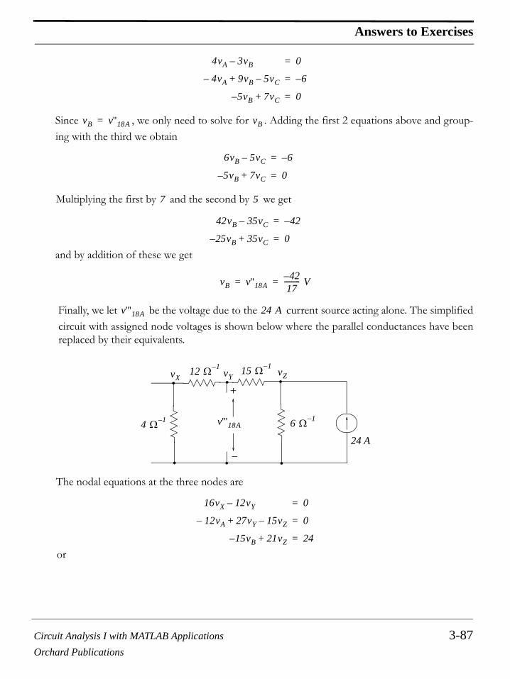
Circuit Analysis I with MATLAB Applications 3-87Orchard Publications
Answers to Exercises
Since , we only need to solve for . Adding the first 2 equations above and group-ing with the third we obtain
Multiplying the first by and the second by we get
and by addition of these we get
Finally, we let be the voltage due to the current source acting alone. The simplifiedcircuit with assigned node voltages is shown below where the parallel conductances have beenreplaced by their equivalents.
The nodal equations at the three nodes are
or
4vA 3vB – 0=
4vA– 9vB 5vC–+ 6–=
5– vB 7vC+ 0=
vB v''18A= vB
6vB 5vC– 6–=
5– vB 7vC+ 0=
7 5
42vB 35vC– 42–=
25– vB 35vC+ 0=
vB v''18A42–
17--------- V= =
v'''18A 24 A
24 A
+
−
15 Ω 1–
4 Ω 1– 6 Ω 1–
12 Ω 1–
v'''18A
vX vY vZ
16vX 12vY – 0=
12vA– 27vY 15vZ–+ 0=
15– vB 21vZ+ 24=
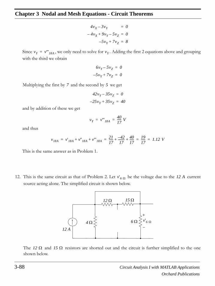
Chapter 3 Nodal and Mesh Equations - Circuit Theorems
3-88 Circuit Analysis I with MATLAB ApplicationsOrchard Publications
Since , we only need to solve for . Adding the first 2 equations above and groupingwith the third we obtain
Multiplying the first by and the second by we get
and by addition of these we get
and thus
This is the same answer as in Problem 1.
12. This is the same circuit as that of Problem 2. Let be the voltage due to the currentsource acting alone. The simplified circuit is shown below.
The and resistors are shorted out and the circuit is further simplified to the oneshown below.
4vX 3vY – 0=
4vX– 9vY 5vZ–+ 0=
5– vY 7vZ+ 8=
vY v'''18A= vY
6vY 5vZ– 0=
5– vY 7vZ+ 0=
7 5
42vY 35vZ– 0=
25– vY 35vZ+ 40=
vY v'''18A4017------ V= =
v18A v'18A v''18A v'''18A+ + 2117------ 42–
17--------- 40
17------+ + 19
17------ 1.12 V= = = =
v'6 Ω 12 A
12 A
4 Ω 6 Ω
12 Ω 15 Ω
+
−
v'6 Ω
12 Ω 15 Ω
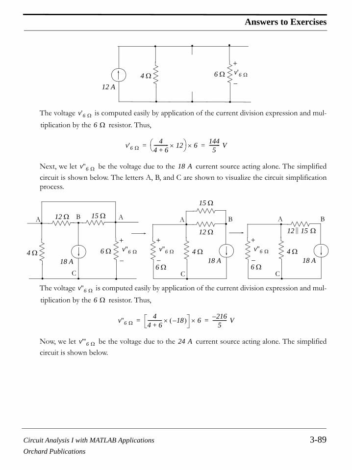
Circuit Analysis I with MATLAB Applications 3-89Orchard Publications
Answers to Exercises
The voltage is computed easily by application of the current division expression and mul-tiplication by the resistor. Thus,
Next, we let be the voltage due to the current source acting alone. The simplifiedcircuit is shown below. The letters A, B, and C are shown to visualize the circuit simplificationprocess.
The voltage is computed easily by application of the current division expression and mul-tiplication by the resistor. Thus,
Now, we let be the voltage due to the current source acting alone. The simplifiedcircuit is shown below.
12 A
4 Ω 6 Ω+
−
v'6 Ω
v'6 Ω
6 Ω
v'6 Ω4
4 6+------------ 12×⎝ ⎠
⎛ ⎞ 6× 1445
--------- V= =
v''6 Ω 18 A
4 Ω 6 Ω
12 Ω 15 Ω
+
−
v''6 Ω
18 A
A B A
C6 Ω
+
−
v''6 Ω
A
4 Ω
12 Ω
15 Ω
B
18 A
C6 Ω
+
−
v''6 Ω
A
4 Ω
B
18 A
C
12 15 Ω||
v''6 Ω
6 Ω
v''6 Ω4
4 6+------------ 18–( )× 6× 216–
5------------ V= =
v'''6 Ω 24 A

Chapter 3 Nodal and Mesh Equations - Circuit Theorems
3-90 Circuit Analysis I with MATLAB ApplicationsOrchard Publications
The and resistors are shorted out and voltage is computed by application ofthe current division expression and multiplication by the resistor. Thus,
Finally, we let be the voltage due to the voltage source acting alone. The simplifiedcircuit is shown below.
By application of the voltage division expression we find that
Therefore,
This is the same answer as that of Problem 2.
13. The circuit for Measurement 1 is shown below.
24 A
4 Ω 6 Ω
12 Ω 15 Ω
+
−
v'''6 Ω
12 Ω 15 Ω v'''6 Ω
6 Ω
v'''6 Ω4
4 6+------------ 24×⎝ ⎠
⎛ ⎞ 6× 2885
--------- V= =
viv6 Ω 36 V
4 Ω 6 Ω
12 Ω 15 Ω
+
−
+ −
36 V
viv6 Ω
+
−36 V
15 Ω
12 Ω
6 Ω
4 ΩA
C
B
A
B
C +
−viv
6 Ω
viv6 Ω
64 6+------------ 36–( )× 108
5---------–= =
v6 Ω v'6 Ω v''6 Ω v'''6 Ω viv6 Ω+ + + 144
5--------- 216
5---------– 288
5--------- 108
5---------–+ 108
5--------- 21.6 V= = = =

Circuit Analysis I with MATLAB Applications 3-91Orchard Publications
Answers to Exercises
Let . Then,
For Measurement 3 the load resistance is the same as for Measurement 1 and the load current isgiven as . Therefore, for Measurement 3 we find that
and we enter this value in the table below.
The circuit for Measurement 2 is shown below.
Let . Then,
For Measurement 4 the load resistance is the same as for Measurement 2 and is given as. Therefore, for Measurement 4 we find that
and we enter this value in the table below.
The circuit for Measurement 5 is shown below.
1 Ω
48 V
+−
iLOAD116 A
RLOAD1
RS1
vS1
Req1 RS1 RLOAD1+=
Req1vS1
iLOAD1---------------- 48
16------ 3 Ω= = =
5 A–
vS1 Req1 5–( ) 3 5–( )× 15 V–= = =
1 Ω
36 V
+−
iLOAD26 A
RLOAD2
RS2
vS2
Req2 RS1 RLOAD2+=
Req2vS2
iLOAD2---------------- 36
6------ 6 Ω= = =
vS2
42 V–
iLOAD2vS2
Req2---------- 42
6------– 7 A–= = =

Chapter 3 Nodal and Mesh Equations - Circuit Theorems
3-92 Circuit Analysis I with MATLAB ApplicationsOrchard Publications
Replacing the voltage sources with their series resistances to their equivalent current sourceswith their parallel resistances and simplifying, we get the circuit below.
Application of the current division expression yields
and we enter this value in the table below.
The circuit for Measurement 6 is shown below.
We observe that will be zero if and this will occur when . This can beshown to be true by writing a nodal equation at Node A. Thus,
+
−
+
−
1 Ω
1 Ω
vS2
vS1RS2
RS1
iLOAD
vLOADRLOAD
1 Ω
+
−18 V
15 V
0.5 Ω
iLOAD
RLOAD
1 Ω33 A
iLOAD0.5
0.5 1+---------------- 33× 11 A= =
+
−
1 Ω
1 Ω
vS2
vS1RS2
RS1
iLOAD
RLOAD
1 Ω
+
−24 V
AvA
iLOAD vA 0= vS1 24–=
vA 24–( )–
1-------------------------
vA 24–
1----------------- 0+ + 0=
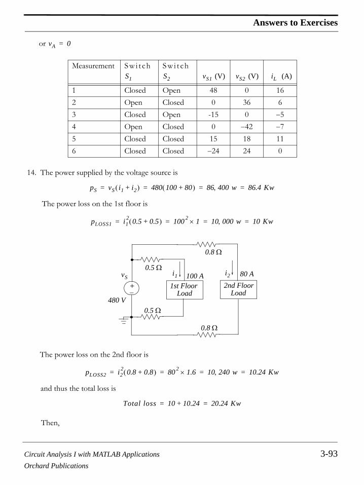
Circuit Analysis I with MATLAB Applications 3-93Orchard Publications
Answers to Exercises
or
14. The power supplied by the voltage source is
The power loss on the 1st floor is
The power loss on the 2nd floor is
and thus the total loss is
Then,
Measurement Sw i t ch S w i t ch (V) (V) (A)
1 Closed Open 48 0 162 Open Closed 0 36 63 Closed Open -15 0 −54 Open Closed 0 −42 −75 Closed Closed 15 18 116 Closed Closed −24 24 0
vA 0=
S1 S2 vS1 vS2 iL
pS vS i1 i2+( ) 480 100 80+( ) 86 400 w, 86.4 Kw= = = =
pLOSS1 i12 0.5 0.5+( ) 100 2 1× 10 000 w, 10 Kw= = = =
480 V
0.8 Ω
+−+−
0.5 Ω
0.5 Ω
1st FloorLoad
100 A2nd Floor
Load
0.8 Ω
80 AvSi2i1
pLOSS2 i22 0.8 0.8+( ) 80 2 1.6× 10 240 w, 10.24 Kw= = = =
Total loss 10 10.24+ 20.24 Kw= =

Chapter 3 Nodal and Mesh Equations - Circuit Theorems
3-94 Circuit Analysis I with MATLAB ApplicationsOrchard Publications
and
This is indeed a low efficiency.
15. The voltage drop on the second floor conductor is
and thus the full-load voltage is
Then,
This is a very poor regulation.
16. We assign node voltages and we write nodal equations as shown below.
Output power Input power power losses– 86.4 20.24– 66.16Kw= = =
% Efficiency η OutputInput
------------------ 100× 66.1686.4
------------- 100× 76.6%= = = =
vcond RT i2 1.6 80× 128 V= = =
480 V
0.8 Ω
+−+−
0.5 Ω
0.5 Ω
1st FloorLoad
100 A2nd Floor
Load
0.8 Ω
80 AVS i1i2
vFL 480 128– 352 V= =
% RegulationvNL vFL–
vFL---------------------- 100× 480 352–
352------------------------ 100× 36.4%= = =
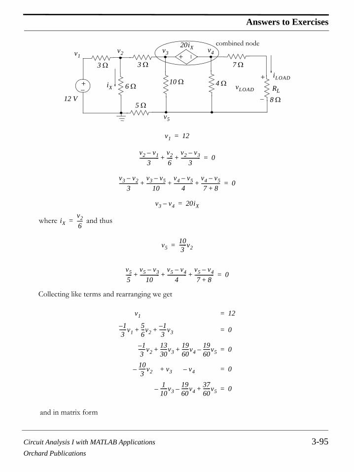
Circuit Analysis I with MATLAB Applications 3-95Orchard Publications
Answers to Exercises
where and thus
Collecting like terms and rearranging we get
and in matrix form
+ −
12 V
+−+−
3 Ω 3 Ω
5 Ω
6 Ω10 Ω
7 Ω
8 Ω
RL
+
−
4 ΩiLOAD
iX
20iX
vLOAD
v1v4v3
v5
v2
combined node
v1 12=
v2 v1–
3----------------
v26-----
v2 v3–
3----------------+ + 0=
v3 v2–
3----------------
v3 v5–
10----------------
v4 v5–
4----------------
v4 v5–
7 8+----------------+ + + 0=
v3 v4– 20iX=
iXv26-----=
v5103------v2=
v55-----
v5 v3–
10----------------
v5 v4–
4----------------
v5 v4–
7 8+----------------+ + + 0=
v1 12=
1–3
------v156---v2
1–3
------v3 + + 0=
1–3
------v21330------v3
1960------v4
1960------v5–+ + 0=
103
------v2 – v3 v4 –+ 0=
110------v3–
1960------v4–
3760------v5+ 0=
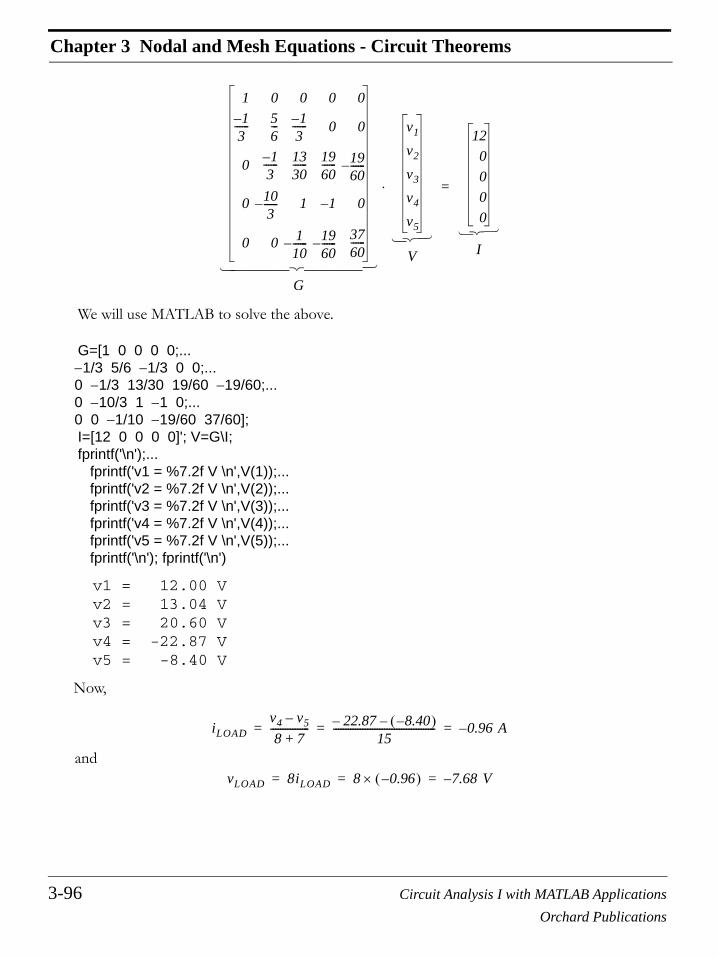
Chapter 3 Nodal and Mesh Equations - Circuit Theorems
3-96 Circuit Analysis I with MATLAB ApplicationsOrchard Publications
We will use MATLAB to solve the above.
G=[1 0 0 0 0;... −1/3 5/6 −1/3 0 0;... 0 −1/3 13/30 19/60 −19/60;... 0 −10/3 1 −1 0;... 0 0 −1/10 −19/60 37/60];
I=[12 0 0 0 0]'; V=G\I;fprintf('\n');... fprintf('v1 = %7.2f V \n',V(1));... fprintf('v2 = %7.2f V \n',V(2));... fprintf('v3 = %7.2f V \n',V(3));... fprintf('v4 = %7.2f V \n',V(4));... fprintf('v5 = %7.2f V \n',V(5));... fprintf('\n'); fprintf('\n')
v1 = 12.00 V v2 = 13.04 V v3 = 20.60 V v4 = -22.87 V v5 = -8.40 V
Now,
and
1 0 0 0 01–
3------ 5
6--- 1–
3------ 0 0
0 1–3
------ 1330------ 19
60------ 19
60------–
0 103
------– 1 1– 0
0 0 110------– 19
60------–
3760------
G
v1
v2
v3
v4
v5
V
⋅
120000
I
=
⎧ ⎪ ⎪ ⎪ ⎪ ⎨ ⎪ ⎪ ⎪ ⎪ ⎩
⎧ ⎨ ⎩ ⎧ ⎨ ⎩
iLOADv4 v5–
8 7+---------------- 22.87– 8.40–( )–
15------------------------------------------ 0.96 A–= = =
vLOAD 8iLOAD 8 0.96–( )× 7.68 V–= = =

Circuit Analysis I with MATLAB Applications 4-1Orchard Publications
Chapter 4
Introduction to Operational Amplifiers
his chapter is an introduction to amplifiers. It discusses amplifier gain in terms of decibels (dB)and provides an overview of operational amplifiers, their characteristics and applications.Numerous formulas for the computation of the gain are derived and several practical examples
are provided.
4.1 Signals
A signal is any waveform that serves as a means of communication. It represents a fluctuating electricquantity, such as voltage, current, electric or magnetic field strength, sound, image, or any messagetransmitted or received in telegraphy, telephony, radio, television, or radar. A typical signal which var-ies with time is shown in figure 4.1 where can be any physical quantity such as voltage, current,temperature, pressure, and so on.
Figure 4.1. A signal that changes with time
4.2 Amplifiers
An amplifier is an electronic circuit which increases the magnitude of the input signal. The symbol ofa typical amplifier is a triangle as shown in Figure 4.2.
Figure 4.2. Symbol for electronic amplifier
An electronic (or electric) circuit which produces an output that is smaller than the input is called anattenuator. A resistive voltage divider is a typical attenuator.
T
f t( )
t
f t( )
vin vout
Electronic Amplifier

Chapter 4 Introduction to Operational Amplifiers
4-2 Circuit Analysis I with MATLAB ApplicationsOrchard Publications
An amplifier can be classified as a voltage amplifier, current amplifier, or power amplifier.
The gain of an amplifier is the ratio of the output to the input. Thus for a voltage amplifier,
or
(4.1)
The current gain and power gain are defined similarly.
Note 1: Throughout this text, the common (base 10) logarithm of a number x will be denoted as while its natural (base e) logarithm will be denoted as .
4.3 Decibels
The ratio of any two values of the same quantity (power, voltage or current) can be expressed in. For instance, we say that an amplifier has power gain or a transmission line
has a power loss of (or gain ). If the gain (or loss) is , the output is equal to theinput.
We must remember that a negative voltage or current gain or indicates that there is a phase difference between the input and the output waveforms. For instance, if an amplifier has again of −100 (dimensionless number), it means that the output is 180 degrees out-of-phase with theinput. Therefore, to avoid misinterpretation of gain or loss, we use absolute values of power, voltageand current when these are expressed in dB.
By definition,
(4.2)
Therefore,
It is useful to remember that
Voltage Gain Output VoltageInput Voltage
-----------------------------------------=
Gvvoutvin---------=
Gi Gp
x( )log x( )ln
decibels dB( ) 10 dB7 dB 7– dB 0 dB
Gv Gi 180°
dB 10poutpin----------log=
10 dB represents a power ratio of 10
10n dB represents a power ratio of 10 n
20 dB represents a power ratio of 10030 dB represents a power ratio of 100060 dB represents a power ratio of 1000000
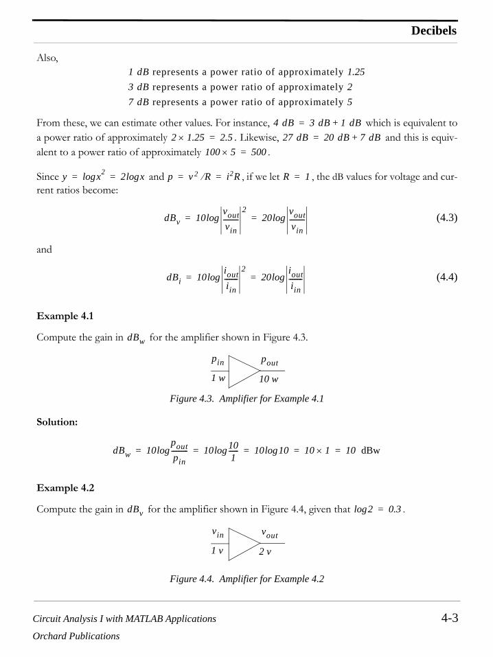
Circuit Analysis I with MATLAB Applications 4-3Orchard Publications
Decibels
Also,
From these, we can estimate other values. For instance, which is equivalent toa power ratio of approximately . Likewise, and this is equiv-alent to a power ratio of approximately .
Since and , if we let , the dB values for voltage and cur-rent ratios become:
(4.3)
and
(4.4)
Example 4.1
Compute the gain in for the amplifier shown in Figure 4.3.
Figure 4.3. Amplifier for Example 4.1
Solution:
Example 4.2
Compute the gain in for the amplifier shown in Figure 4.4, given that .
Figure 4.4. Amplifier for Example 4.2
1 dB represents a power ratio of approximately 1.253 dB represents a power ratio of approximately 27 dB represents a power ratio of approximately 5
4 dB 3 dB 1 dB+=
2 1.25× 2.5= 27 dB 20 dB 7 dB+=
100 5× 500=
y x2log 2 xlog= = p v 2 R⁄ i2R= = R 1=
dBv 10voutvin---------
2log 20
voutvin---------log= =
dBi 10ioutiin--------
2log 20
ioutiin--------log= =
dBw
1 w 10 w
pin pout
dBw 10poutpin----------log 10 10
1------log 10 10log 10 1× 10 dBw= = = = =
dBv 2log 0.3=
1 v 2 v
vin vout

Chapter 4 Introduction to Operational Amplifiers
4-4 Circuit Analysis I with MATLAB ApplicationsOrchard Publications
Solution:
4.4 Bandwidth and Frequency Response
Like electric filters, amplifiers exhibit a band of frequencies over which the output remains nearlyconstant. Consider, for example, the magnitude of the output voltage of an electric or elec-tronic circuit as a function of radian frequency as shown in Figure 4.5.
Figure 4.5. Typical bandwidth of an amplifier
As shown above, the bandwidth is where and are the lower and upper cutoff fre-
quencies respectively. At these frequencies, and these two points are knownas the 3-dB down or half-power points. They derive their name from the fact that power
, and for and or , the power is, that is, the power is “halved”. Alternately, we can define the bandwidth as the frequency band
between half-power points.
Most amplifiers are used with a feedback path which returns (feeds) some or all its output to the inputas shown in Figure 4.6.
Figure 4.6. Gain amplifiers used with feedback
In Figure 4.6, the symbol Σ (Greek capital letter sigma) inside the circle denotes the summing pointwhere the output signal, or portion of it, is combined with the input signal. This summing point may
dBv 20voutvin---------log 20 2
1---log 20 0.3log 20 0.3× 6 dBv= = = = =
vout
ω
1
0.707
ω
Bandwidth
vout
ω1 ω2
BW ω2 ω1–= ω1 ω2
vout 2 2⁄ 0.707= =
p v 2 R⁄ i2R= = R 1= v 2 2⁄ 0.707= = i 2 2⁄ 0.707= =
1 2⁄
ΣIn Out
+−
Partial Output Feedback
ΣIn Out
+−
Entire Output Feedback
Gain Amplifier Gain Amplifier
Feedback PathFeedback Circuit

Circuit Analysis I with MATLAB Applications 4-5Orchard Publications
The Operational Amplifier
be also indicated with a large plus (+) symbol inside the circle. The positive (+) sign below the sum-ming point implies positive feedback which means that the output, or portion of it, is added to theinput. On the other hand, the negative (−) sign implies negative feedback which means that the output,or portion of it, is subtracted from the input. Practically, all amplifiers use used with negative feed-back since positive feedback causes circuit instability.
4.5 The Operational Amplifier
The operational amplifier or simply op amp is the most versatile electronic amplifier. It derives it namefrom the fact that it is capable of performing many mathematical operations such as addition, multi-plication, differentiation, integration, analog-to-digital conversion or vice versa. It can also be usedas a comparator and electronic filter. It is also the basic block in analog computer design. Its symbolis shown in Figure 4.7.
Figure 4.7. Symbol for operational amplifier
As shown above the op amp has two inputs but only one output. For this reason it is referred to asdifferential input, single ended output amplifier. Figure 4.8 shows the internal construction of a typical opamp. This figure also shows terminals and . These are the voltage sources required topower up the op amp. Typically, is +15 volts and is −15 volts. These terminals are notshown in op amp circuits since they just provide power, and do not reveal any other useful informa-tion for the op amp’s circuit analysis.
4.6 An Overview of the Op Amp
The op amp has the following important characteristics:
1. Very high input impedance (resistance)
2. Very low output impedance (resistance)
3. Capable of producing a very large gain that can be set to any value by connection of externalresistors of appropriate values
4. Frequency response from DC to frequencies in the MHz range
5. Very good stability
6. Operation to be performed, i.e., addition, integration etc. is done externally with proper selectionof passive devices such as resistors, capacitors, diodes, and so on.
1
23
+−
VCC VEE
VCC VEE

Chapter 4 Introduction to Operational Amplifiers
4-6 Circuit Analysis I with MATLAB ApplicationsOrchard Publications
Figure 4.8. Internal Devices of a Typical Op Amp
An op amp is said to be connected in the inverting mode when an input signal is connected to theinverting (−) input through an external resistor whose value along with the feedback resistor determine the op amp’s gain. The non-inverting (+) input is grounded through an external resistor Ras shown in Figure 4.9.
For the circuit of Figure 4.9, the voltage gain is
(4.5)
VCC
VEE
1 2
1 NON-INVERTING INPUT2 INVERTING INPUT3 OUTPUT
3
Rin Rf
Gv
Gvvoutvin---------
RfRin--------–= =
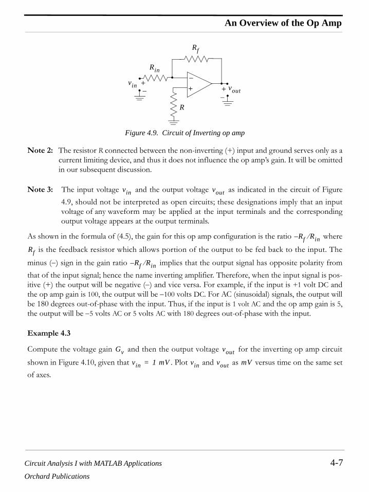
Circuit Analysis I with MATLAB Applications 4-7Orchard Publications
An Overview of the Op Amp
Figure 4.9. Circuit of Inverting op amp
Note 2: The resistor R connected between the non-inverting (+) input and ground serves only as acurrent limiting device, and thus it does not influence the op amp’s gain. It will be omittedin our subsequent discussion.
Note 3: The input voltage and the output voltage as indicated in the circuit of Figure4.9, should not be interpreted as open circuits; these designations imply that an inputvoltage of any waveform may be applied at the input terminals and the correspondingoutput voltage appears at the output terminals.
As shown in the formula of (4.5), the gain for this op amp configuration is the ratio where is the feedback resistor which allows portion of the output to be fed back to the input. The
minus (−) sign in the gain ratio implies that the output signal has opposite polarity fromthat of the input signal; hence the name inverting amplifier. Therefore, when the input signal is pos-itive (+) the output will be negative (−) and vice versa. For example, if the input is +1 volt DC andthe op amp gain is 100, the output will be −100 volts DC. For AC (sinusoidal) signals, the output willbe 180 degrees out-of-phase with the input. Thus, if the input is 1 volt AC and the op amp gain is 5,the output will be −5 volts AC or 5 volts AC with 180 degrees out-of-phase with the input.
Example 4.3
Compute the voltage gain and then the output voltage for the inverting op amp circuitshown in Figure 4.10, given that . Plot and as versus time on the same setof axes.
+−
R
+
−− +
vin
Rf
vout
Rin
vin vout
Rf Rin⁄–
Rf
Rf Rin⁄–
Gv vout
vin 1 mV= vin vout mV

Chapter 4 Introduction to Operational Amplifiers
4-8 Circuit Analysis I with MATLAB ApplicationsOrchard Publications
Figure 4.10. Circuit for Example 4.3
Solution:
This is an inverting amplifier and thus the voltage gain is
or
and since
the output voltage is
or
The voltages and are plotted as shown in Figure 4.11.
Figure 4.11. Input and output waveforms for the circuit of Example 4.3
+−
+
−− +
Rin
Rf
vin vout
120 KΩ
20 KΩ
Gv
GvRfRin--------– 120 KΩ
20 KΩ--------------------–= =
Gv 6–=
Gvvoutvin---------=
vout Gvvin 6 1×–= =
vout 6 mV–=
vin vout
-7-6-5-4-3-2-1012
Time
v OU
T / v
IN (m
illivo
lts)
vIN = 1 mV
vOUT = −6 mV
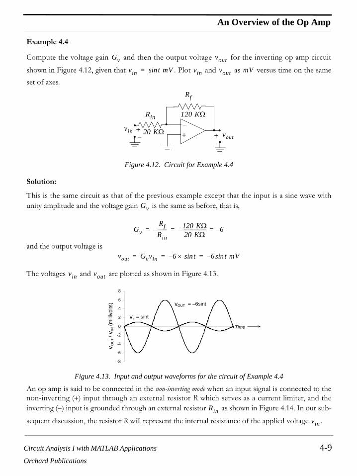
Circuit Analysis I with MATLAB Applications 4-9Orchard Publications
An Overview of the Op Amp
Example 4.4
Compute the voltage gain and then the output voltage for the inverting op amp circuitshown in Figure 4.12, given that . Plot and as versus time on the sameset of axes.
Figure 4.12. Circuit for Example 4.4
Solution:
This is the same circuit as that of the previous example except that the input is a sine wave withunity amplitude and the voltage gain is the same as before, that is,
and the output voltage is
The voltages and are plotted as shown in Figure 4.13.
Figure 4.13. Input and output waveforms for the circuit of Example 4.4
An op amp is said to be connected in the non-inverting mode when an input signal is connected to thenon-inverting (+) input through an external resistor R which serves as a current limiter, and theinverting (−) input is grounded through an external resistor as shown in Figure 4.14. In our sub-sequent discussion, the resistor R will represent the internal resistance of the applied voltage .
Gv vout
vin t sin mV= vin vout mV
+−
+
−− +
Rin
Rf
vin vout
120 KΩ
20 KΩ
Gv
GvRfRin--------– 120 KΩ
20 KΩ-------------------- 6–=–= =
vout Gvvin 6 tsin×– 6 t sin mV–= = =
vin vout
-8
-6
-4
-2
0
2
4
6
8
v OU
T / v
IN (m
illivo
lts)
vin = sint
vOUT = −6sint
Time
Rin
vin
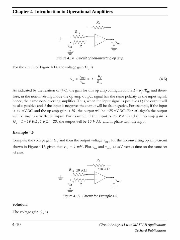
Chapter 4 Introduction to Operational Amplifiers
4-10 Circuit Analysis I with MATLAB ApplicationsOrchard Publications
Figure 4.14. Circuit of non-inverting op amp
For the circuit of Figure 4.14, the voltage gain is
(4.6)
As indicated by the relation of (4.6), the gain for this op amp configuration is and there-fore, in the non-inverting mode the op amp output signal has the same polarity as the input signal;hence, the name non-inverting amplifier. Thus, when the input signal is positive (+) the output willbe also positive and if the input is negative, the output will be also negative. For example, if the inputis and the op amp gain is , the output will be . For AC signals the outputwill be in-phase with the input. For example, if the input is and the op amp gain is
, the output will be and in-phase with the input.
Example 4.5
Compute the voltage gain and then the output voltage for the non-inverting op amp circuitshown in Figure 4.15, given that . Plot and as versus time on the same setof axes.
Figure 4.15. Circuit for Example 4.5
Solution:
The voltage gain is
+−
R+
−−
+ voutvin
Rin
Rf
Gv
Gvvoutvin--------- 1
RfRin--------+= =
1 Rf Rin⁄+
+1 mV DC 75 +75 mV DC0.5 V AC
Gv 1 19 KΩ 1 KΩ⁄+ 20== 10 V AC
Gv vout
vin 1 mV= vin vout mV
+−
R+
−−
+ voutvin
Rin
Rf
20 KΩ 120 KΩ
Gv
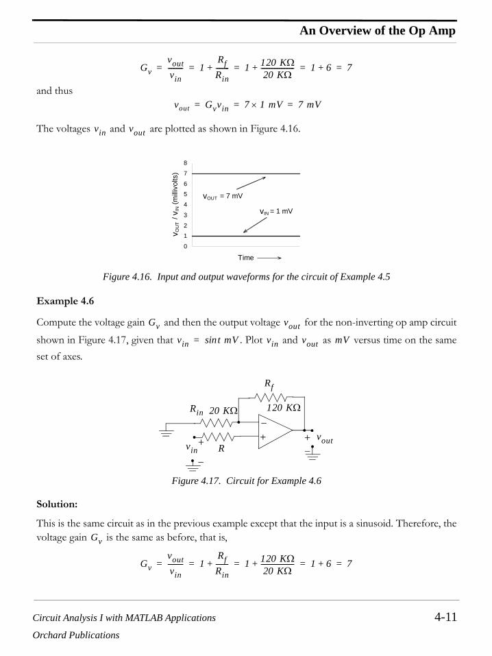
Circuit Analysis I with MATLAB Applications 4-11Orchard Publications
An Overview of the Op Amp
and thus
The voltages and are plotted as shown in Figure 4.16.
Figure 4.16. Input and output waveforms for the circuit of Example 4.5
Example 4.6
Compute the voltage gain and then the output voltage for the non-inverting op amp circuitshown in Figure 4.17, given that . Plot and as versus time on the sameset of axes.
Figure 4.17. Circuit for Example 4.6
Solution:
This is the same circuit as in the previous example except that the input is a sinusoid. Therefore, thevoltage gain is the same as before, that is,
Gvvoutvin--------- 1
RfRin--------+ 1 120 KΩ
20 KΩ--------------------+ 1 6+ 7= = = = =
vout Gvvin 7 1× mV 7 mV= = =
vin vout
0
1
2
3
4
5
6
7
8
Time
v OU
T /
v IN (m
illivo
lts)
vIN = 1 mV
vOUT = 7 mV
Gv vout
vin t sin mV= vin vout mV
+−
R+
−−
+ voutvin
Rin
Rf
20 KΩ 120 KΩ
Gv
Gvvoutvin--------- 1
RfRin--------+ 1 120 KΩ
20 KΩ--------------------+ 1 6+ 7= = = = =

Chapter 4 Introduction to Operational Amplifiers
4-12 Circuit Analysis I with MATLAB ApplicationsOrchard Publications
and the output voltage is
The voltages and are plotted as shown in Figure 4.18.
Figure 4.18. Input and output waveforms for the circuit of Example 4.6
Quite often an op amp is connected as shown in Figure 4.19.
Figure 4.19. Circuit of unity gain op amp
For the circuit of Figure 4.19, the voltage gain is
(4.7)
and thus
(4.8)
For this reason, the op amp circuit of Figure 4.19 it is called unity gain amplifier. For example, if theinput voltage is the output will also be , and if the input voltage is ,the output will also be . The unity gain op amp is used to provide a very high resistancebetween a voltage source and the load connected to it. An example will be given in Section 4.8.
vout Gvvin 7 tsin× 7 t sin mV= = =
vin vout
-8
-6
-4
-2
0
2
4
6
8
v OU
T /
v IN (m
illivo
lts)
vIN = sint
vOUT = 7sint
Time
+−
R+ −
−
+vin
vout
Gv
Gvvoutvin--------- 1= =
vout vin=
5 mV DC 5 mV DC 2 mV AC2 mV AC

Circuit Analysis I with MATLAB Applications 4-13Orchard Publications
Active Filters
4.7 Active Filters
An active filter is an electronic circuit consisting of an amplifier and other devices such as resistorsand capacitors. In contrast, a passive filter is a circuit which consists of passive devices such as resis-tors, capacitors and inductors. Operational amplifiers are used extensively as active filters.
A low-pass filter transmits (passes) all frequencies below a critical (cutoff ) frequency denoted as , andattenuates (blocks) all frequencies above this cutoff frequency. An op amp low-pass filter is shown inFigure 4.20 and its frequency response in Figure 4.21.
Figure 4.20. A low-pass active filter
Figure 4.21. Frequency response for amplitude of a low-pass filter
In Figure 4.21, the straight vertical and horizontal lines represent the ideal (unrealizable) and thesmooth curve represents the practical (realizable) low-pass filter characteristics. The vertical scalerepresents the magnitude of the ratio of output-to-input voltage , that is, the gain . Thecutoff frequency is the frequency at which the maximum value of which is unity, fallsto , and as mentioned before, this is the half power or the point.
ωC
vin vout
Low Pass Filter Frequency Respone
0
0.2
0.4
0.6
0.8
1
Radian Frequency (log scale)
|vO
UT
/ vIN
|
ωc
Ideal
Realizable
Half-Power Point
ω
vout vin⁄ Gv
ωc vout vin⁄
0.707 Gv× 3 dB–

Chapter 4 Introduction to Operational Amplifiers
4-14 Circuit Analysis I with MATLAB ApplicationsOrchard Publications
A high-pass filter transmits (passes) all frequencies above a critical (cutoff) frequency , and attenu-ates (blocks) all frequencies below the cutoff frequency. An op amp high-pass filter is shown in Fig-ure 4.22 and its frequency response in Figure 4.23.
Figure 4.22. A high-pass active filter
Figure 4.23. Frequency response for amplitude of a high-pass filter
In Figure 4.23, the straight vertical and horizontal lines represent the ideal (unrealizable) and thesmooth curve represents the practical (realizable) high-pass filter characteristics. The vertical scalerepresents the magnitude of the ratio of output-to-input voltage , that is, the gain . Thecutoff frequency is the frequency at which the maximum value of which is unity, falls to
, i.e., the half power or the point.
A band-pass filter transmits (passes) the band (range) of frequencies between the critical (cutoff) fre-quencies denoted as and , where the maximum value of which is unity, falls to ,
while it attenuates (blocks) all frequencies outside this band. An op amp band-pass filter and its fre-quency response are shown below. An op amp band-pass filter is shown in Figure 4.24 and its fre-quency response in Figure 4.25.
ωc
vin vout
High-pass Filter Frequency Response
0.0
0.2
0.4
0.6
0.8
1.0
Radian Frequency (log scale)
|vO
UT
/ vIN
|
ωc
Ideal
Realizable
ω
Half-Power Point
vout vin⁄ Gv
ωc vout vin⁄
0.707 Gv× 3 dB–
ω1 ω2 Gv 0.707 Gv×

Circuit Analysis I with MATLAB Applications 4-15Orchard Publications
Active Filters
Figure 4.24. An active band-pass filter
Figure 4.25. Frequency response for amplitude of a band-pass filter
A band-elimination or band-stop or band-rejection filter attenuates (rejects) the band (range) of frequen-cies between the critical (cutoff) frequencies denoted as and , where the maximum value of
which is unity, falls to , while it transmits (passes) all frequencies outside this band.An op amp band-stop filter is shown in Figure 4.26 and its frequency response in Figure 4.27.
vin vout
ωcω
Half-Power Point
Band Pass Filter Frequency Response
00.10.20.30.40.50.60.70.80.9
1
Radian Frequency (log scale)
|vO
UT
/ vIN
|
ω1 ω2ω
Half-Power Points
Ideal
Realizable
ω1 ω2
Gv 0.707 Gv×

Chapter 4 Introduction to Operational Amplifiers
4-16 Circuit Analysis I with MATLAB ApplicationsOrchard Publications
Figure 4.26. An active band-elimination filter
Figure 4.27. Frequency response for amplitude of a band-elimination filter
4.8 Analysis of Op Amp Circuits
The procedure for analyzing an op amp circuit (finding voltages, currents and power) is the same asfor the other circuits which we have studied thus far. That is, we can apply Ohm’s law, KCL andKVL, superposition, Thevenin’s and Norton’s theorems. When analyzing an op amp circuit, we mustremember that in any op-amp:
a. The currents into both input terminals are zero
b. The voltage difference between the input terminals of an op amp is zero
c. For circuits containing op amps, we will assume that the reference (ground) is the common terminal of thetwo power supplies. For simplicity, the power supplies will not be shown.
vinvout
Band Elimination Active Filter Circuit
ωcω
Half-Power Point
Band-Elimination Filter Frequency Response
00.10.20.30.40.50.60.70.80.9
1
Radian Frequency (log scale)
|vO
UT
/ vIN
|
ω1 ω2ω
Half-Power Points
Ideal
Realizable

Circuit Analysis I with MATLAB Applications 4-17Orchard Publications
Analysis of Op Amp Circuits
We will provide several examples to illustrate the analysis of op amp circuits without being con-cerned about its internal operation; this is discussed in electronic circuit analysis books.
Example 4.7
The op amp circuit shown in Figure 4.28 is called inverting op amp. Prove that the voltage gain isas given in (4.9) below, and draw its equivalent circuit showing the output as a dependent source.
Figure 4.28. Circuit for deriving the gain of an inverting op amp
(4.9)
Proof:
No current flows through the (−) input terminal of the op amp; therefore the current which flowsthrough resistor flows also through resistor . Also, since the (+) input terminal is groundedand there is no voltage drop between the (−) and (+) terminals, the (−) input is said to be at virtualground. From the circuit of Figure 4.28,
where
and thus
or
Gv
+−
R
+
−− +
vin
Rf
vout
Rin
i
i
Gvvoutvin---------
RfRin--------–= =
iRin Rf
vout Rf i–=
ivinRin--------=
voutRfRin--------– vin=
Gvvoutvin---------
RfRin--------–= =

Chapter 4 Introduction to Operational Amplifiers
4-18 Circuit Analysis I with MATLAB ApplicationsOrchard Publications
The input and output parts of the circuit are shown in Figure 4.29 with the virtual ground being thesame as the circuit ground.
Figure 4.29. Input and output parts of the inverting op amp
These two circuits are normally drawn with the output as a dependent source as shown in Figure4.30. This is the equivalent circuit of the inverting op amp and, as mentioned in Chapter 1, the dependentsource is a Voltage Controlled Voltage Source (VCVS).
Figure 4.30. Equivalent circuit of the inverting op amp
Example 4.8
The op amp circuit shown in Figure 4.31 is called non-inverting op amp. Prove that the voltage gain is as given in (4.10) below, and draw its equivalent circuit showing the output as a dependent source.
Figure 4.31. Circuit of non-inverting op amp
(4.10)
+
−+
−−+
i−
+ ivin voutRfRin
+−+
−−
+
vin
Rin voutRfRin--------vin
Gv
+−
+−
−
+ voutvin
Rin
Rf
Gvvoutvin--------- 1
RfRin--------+= =

Circuit Analysis I with MATLAB Applications 4-19Orchard Publications
Analysis of Op Amp Circuits
Proof:
Let the voltages at the (−) and (+) terminals be denoted as and respectively as shown in Figure4.32.
Figure 4.32. Non-inverting op amp circuit for derivation of (4.10)
By application of KCL at
or
(4.11)
There is no potential difference between the (−) and (+) terminals; therefore, or
. Relation (4.11) then can be written as
or
Rearranging, we get
and its equivalent circuit is as shown in Figure 4.33. The dependent source of this equivalent circuitis also a VCVS.
v1 v2
+
−
+ −
−
+
+ −Rf
Rin
i1
i2
vin
vout
v1
v2
v1
i1 i2+ 0=
v1Rin--------
v1 vout–
Rf--------------------+ 0=
v1 v2– 0=
v1 v2 vin= =
vinRin--------
vin vout–
Rf----------------------+ 0=
1Rin-------- 1
Rf-----+⎝ ⎠
⎛ ⎞ vinvoutRf
---------=
Gvvoutvin--------- 1
RfRin--------+= =

Chapter 4 Introduction to Operational Amplifiers
4-20 Circuit Analysis I with MATLAB ApplicationsOrchard Publications
Figure 4.33. Equivalent circuit of the non-inverting op amp
Example 4.9
If, in the non-inverting op amp circuit of the previous example, we replace with an open circuit( ) and with a short circuit ( ), prove that the voltage gain is
(4.12)
and thus
(4.13)
Proof:
With open and shorted, the non-inverting amplifier of the previous example reduces to thecircuit of Figure 4.34.
Figure 4.34. Circuit of Figure 4.32 with open and shorted
The voltage difference between the (+) and (−) terminals is zero; then .
We will obtain the same result if we consider the non-inverting op amp gain .
Then, letting , the gain reduces to and for this reason this circuit is called unity gain
+
−−
++−
1RfRin--------+
⎝ ⎠⎜ ⎟⎛ ⎞
vin voutvin
Rin
Rin ∞→ Rf Rf 0→ Gv
Gvvoutvin--------- 1= =
vout vin=
Rin Rf
+−
+ −
−
+ voutvin
Rin Rf
vout vin=
Gvvoutvin--------- 1
RfRin--------+= =
Rf 0→ Gv 1=

Circuit Analysis I with MATLAB Applications 4-21Orchard Publications
Analysis of Op Amp Circuits
amplifier or voltage follower. It is also called buffer amplifier because it can be used to “buffer” (isolate)one circuit from another when one “loads” the other as we will see on the next example.
Example 4.10
For the circuit of Figure4.35
a. With the load disconnected, compute the open circuit voltage
b. With the load connected, compute the voltage across the load
c. Insert a buffer amplifier between a and b and compute the new voltage across the sameload
Figure 4.35. Circuit for Example 4.10
Solution:
a. With the load disconnected the circuit is as shown in Figure 4.36.
Figure 4.36. Circuit for Example 4.10 with the load disconnected
The voltage across terminals a and b is
b. With the load reconnected the circuit is as shown in Figure 4.37.
RLOAD vab
vLOAD RLOAD
vLOAD
RLOAD
+−
12 V
×
×a
b
vin
RLOAD
7 KΩ
5 KΩ5 KΩ
RLOAD
+−
12 V
×
×a
b
vin
RLOAD
7 KΩ
5 KΩ5KΩ
vab5 KΩ
7 KΩ 5 KΩ+----------------------------------= 12× 5 V=
RLOAD

Chapter 4 Introduction to Operational Amplifiers
4-22 Circuit Analysis I with MATLAB ApplicationsOrchard Publications
Figure 4.37. Circuit for Example 4.10 with the load reconnected
Here, we observe that the load “loads down” the load voltage from to andthis voltage may not be sufficient for proper operation of the load.
c. With the insertion of the buffer amplifier between points a and b and the load, the circuit now isas shown in Figure 4.38.
Figure 4.38. Circuit for Example 4.10 with the insertion of a buffer op amp
From the circuit of Figure 4.38, we observe that the voltage across the load is as desired.
Example 4.11
The op amp circuit shown in Figure 4.39 is called summing circuit or summer because the output is thesummation of the weighted inputs. Prove that for this circuit,
(4.14)
+−
12 V
×
×a
b
vin
RLOAD
7 KΩ
5 KΩ5KΩ
vLOAD5 KΩ || 5 KΩ
7 KΩ 5 KΩ || 5 KΩ+-------------------------------------------------------= 12× 3.16 V=
RLOAD 5 V 3.16 V
+−
12 V
×
×a
b
+
−
5 V
+
−vin
7 KΩ
5 KΩ 5 KΩ
RLOADvLOAD vab 5 V= =
5 V
vout Rfvin1Rin1----------
vin2Rin2----------+
⎝ ⎠⎜ ⎟⎛ ⎞
–=

Circuit Analysis I with MATLAB Applications 4-23Orchard Publications
Analysis of Op Amp Circuits
Figure 4.39. Two-input summing op amp circuit
Proof:
We recall that the voltage across the (−) and (+) terminals is zero. We also observe that the (+) inputis grounded, and thus the voltage at the (−) terminal is at “virtual ground”. Then, by application ofKCL at the (−) terminal, we get
and solving for we get (4.14). Alternately, we can apply the principle of superposition to derivethis relation.
Example 4.12
Compute the output voltage for the amplifier circuit shown in Figure 4.40.
Figure 4.40. Circuit for Example 4.12
+−
+
−
+
−+
−
Rf
vout
Rin1
Rin2
vin2
vin1
vin1Rin1----------
vin2Rin2----------
voutRf
---------+ + 0=
vout
vout
+−
+
−
+
−1 mV
4 mV 10 mV
+−
+−
voutvin3
vin1
vin2
Rin2
Rin1
Rin3
Rf 1 MΩ
10 KΩ
20 KΩ 30 KΩ

Chapter 4 Introduction to Operational Amplifiers
4-24 Circuit Analysis I with MATLAB ApplicationsOrchard Publications
Solution:
Let be the output due to acting alone, be the output due to acting alone, and be the output due to acting alone. Then by superposition,
First, with acting alone and and shorted, the circuit becomes as shown in Figure 4.41.
Figure 4.41. Circuit for Example 4.12 with acting alone
We recognize this as an inverting amplifier whose voltage gain is
and thus
(4.15)
Next, with acting alone and and shorted, the circuit becomes as shown in Figure4.42.
The circuit of Figure 4.42 as a non-inverting op amp whose voltage gain is
and the voltage at the plus (+) input is computed from the voltage divider circuit shown in Figure4.43.
vout1 vin1 vout2 vin2
vout3 vin3
vout vout1 vout2 vout3+ +=
vin1 vin2 vin3
+−
+−
+
1 mV
Rin1
10 KΩvin1
Rin2
20 KΩ
Rin3
30 KΩ
Rf
1 MΩ
vout1−
vin1
Gv
Gv 1 MΩ 10 KΩ⁄ 100= =
vout1 100( ) 1 mV–( ) 100 mV–= =
vin2 vin1 vin3
Gv
Gv 1 1 MΩ+ 10 KΩ⁄ 101= =

Circuit Analysis I with MATLAB Applications 4-25Orchard Publications
Analysis of Op Amp Circuits
Figure 4.42. Circuit for Example 4.12 with acting alone
Figure 4.43. Voltage divider circuit for the computation of with acting alone
Then,
and thus
(4.16)
Finally, with acting alone and and shorted, the circuit becomes as shown in Figure4.44.
The circuit of Figure 4.44 is also a non-inverting op amp whose voltage gain is
and the voltage at the plus (+) input is computed from the voltage divider circuit shown in Figure4.45.
+−
+−
+
−
4 mV
Rin1
10 KΩ
Rf
1 MΩ
vout2Rin3
30 KΩvin2
Rin220 KΩ
vin2
+−
4 mV
+
−
30 KΩ
Rin3
Rin2
20 KΩ
To v +( )
vin2
v +( ) vin2
v +( )
Rin3Rin2 Rin3+--------------------------- vin2× 30 KΩ
50 KΩ----------------- 4 mV× 2.4 mV= = =
vout2 101 2.4× mV 242.4 mV= =
vin3 vin1 vin2
Gv
Gv 1 1 MΩ+ 10 KΩ⁄ 101= =
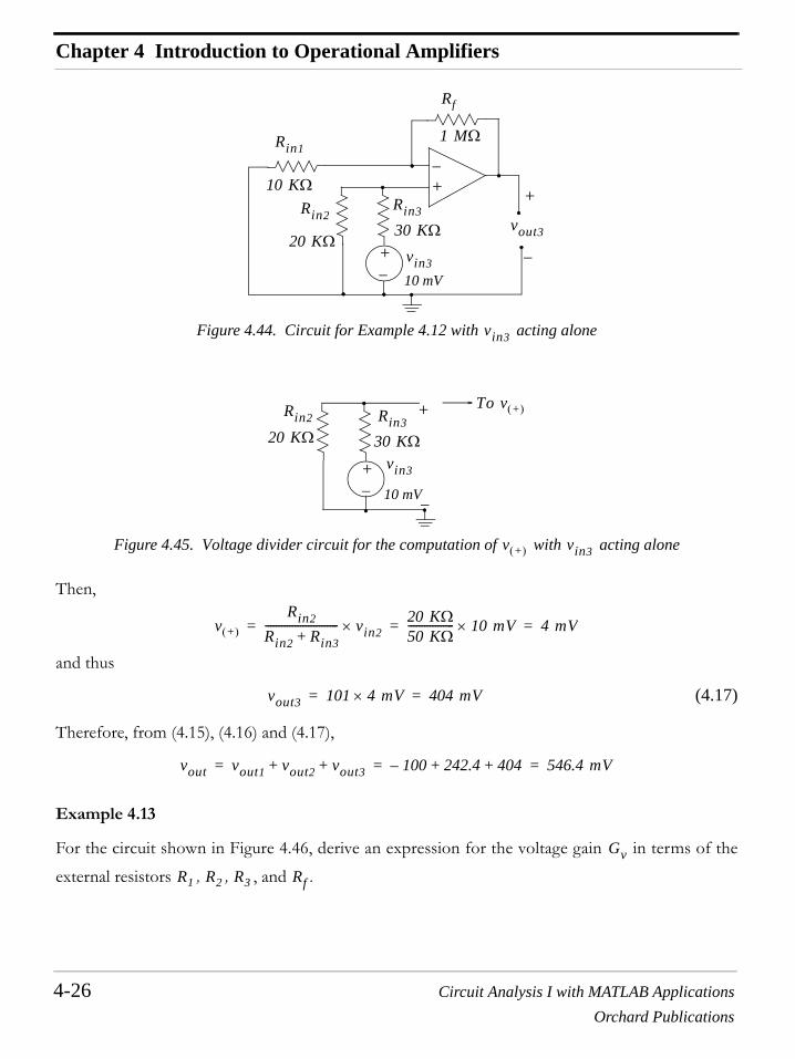
Chapter 4 Introduction to Operational Amplifiers
4-26 Circuit Analysis I with MATLAB ApplicationsOrchard Publications
Figure 4.44. Circuit for Example 4.12 with acting alone
Figure 4.45. Voltage divider circuit for the computation of with acting alone
Then,
and thus
(4.17)
Therefore, from (4.15), (4.16) and (4.17),
Example 4.13
For the circuit shown in Figure 4.46, derive an expression for the voltage gain in terms of theexternal resistors , , , and .
+−
+−
+
−10 mV
Rin1
10 KΩRin2
20 KΩ
Rin3
30 KΩ
vin3
Rf
1 MΩ
vout3
vin3
+− 10 mV
+
−
30 KΩ
Rin3Rin2
20 KΩ
To v +( )
vin3
v +( ) vin3
v +( )
Rin2Rin2 Rin3+--------------------------- vin2× 20 KΩ
50 KΩ----------------- 10 mV× 4 mV= = =
vout3 101 4× mV 404 mV= =
vout vout1 vout2 vout3+ + 100– 242.4 404+ + 546.4 mV= = =
Gv
R1 R2 R3 Rf

Circuit Analysis I with MATLAB Applications 4-27Orchard Publications
Analysis of Op Amp Circuits
Figure 4.46. Circuit for Example 4.13
Solution:
We apply KCL at nodes and as shown in Figure 4.47.
Figure 4.47. Application of KCL for the circuit of Example 4.13
At node :
or
or
or
+−
+
−
+
−
R2
R3
RfR1
vout
vin
v1 v2
+−
+
−
+
−
R2
R3
RfR1
vout
vin
v1
v2
v1
v1 vin–
R1-----------------
v1 vout–
Rf--------------------+ 0=
1R1------ 1
Rf-----+⎝ ⎠
⎛ ⎞ v1vinR1------
voutRf
---------+=
R1 Rf+
R1Rf-----------------
⎝ ⎠⎜ ⎟⎛ ⎞
v1Rf vin R1vout+
R1Rf-----------------------------------=

Chapter 4 Introduction to Operational Amplifiers
4-28 Circuit Analysis I with MATLAB ApplicationsOrchard Publications
(4.18)
At node :
or
(4.19)
and since , we rewrite (4.19) as
(4.20)
Equating the right sides of (4.18) and (4.20) we get
or
Dividing both sides of the above relation by and rearranging, we get
and after simplification
(4.21)
4.9 Input and Output Resistance
The input and output resistances are very important parameters in amplifier circuits.
The input resistance of a circuit is defined as the ratio of the applied voltage to the current drawn by the circuit, that is,
(4.22)
v1Rf vin R1vout+
R1 Rf+-----------------------------------=
v2
v2 vin–
R2-----------------
v2R3------+ 0=
v2R3vin
R2 R3+------------------=
v2 v1=
v1R3vin
R2 R3+------------------=
Rf vin R1vout+
R1 Rf+-----------------------------------
R3vinR2 R3+------------------=
Rf vin R1vout+R3vin
R2 R3+------------------ R1 Rf+( )=
R1vin
voutvin
---------R3 R1 Rf+( )
R1 R2 R3+( )-----------------------------=
RfR1------–
Gvvoutvin
---------R1R3 R2Rf–
R1 R2 R3+( )------------------------------= =
Rin vS iS
RinvSiS-----=

Circuit Analysis I with MATLAB Applications 4-29Orchard Publications
Input and Output Resistance
Therefore, in an op amp circuit the input resistance provides a measure of the current which theamplifier draws from the voltage source . Of course, we want to be as small as possible;accordingly, we must make the input resistance as high as possible.
Example 4.14
Compute the input resistance of the inverting op amp amplifier shown in Figure 4.47 in termsof and .
Figure 4.48. Circuit for Example 4.14
Solution:
By definition,
(4.23)
and since no current flows into the minus (−) terminal of the op amp and this terminal is at virtualground, it follows that
(4.24)
From (4.23) and (4.24) we observe that
(4.25)
It is therefore, desirable to make as high as possible. However, if we make very high such as, for a large gain, say , the value of the feedback resistor should be . Obviously,
this is an impractical value. Fortunately, a large gain can be achieved with the circuit of Problem 8.
Example 4.15
Compute the input resistance of the op amp shown in Figure 4.49.
iS
vS iS
Rin
Rin
R1 Rf
+
−+
−−+
RfR1
vS voutiS
RinvSiS-----=
iSvSR1------=
Rin R1=
R1 R1
10 MΩ 100 Rf 1 GΩ
Rin

Chapter 4 Introduction to Operational Amplifiers
4-30 Circuit Analysis I with MATLAB ApplicationsOrchard Publications
Figure 4.49. Circuit for Example 4.15
Solution:
In the circuit of Figure 4.49, is the voltage at the minus (−) terminal; not the source voltage .Therefore, there is no current drawn by the op amp. In this case, we apply a test (hypothetical)current as shown in Figure 4.49, and we treat as the source voltage.
Figure 4.50. Circuit for Example 4.15 with a test current source
We observe that is zero (virtual ground). Therefore,
By definition, the output resistance is the ratio of the open circuit voltage to the short circuit current, that is,
(4.26)
The output resistance is not the same as the load resistance. The output resistance provides a mea-sure of the change in output voltage when a load which is connected at the output terminals drawscurrent from the circuit. It is desirable to have an op amp with very low output resistance as illus-trated by the following example.
+−
−+
Rf
vout
vin
100 KΩ
vin vS
iS
iX vin
+−
−+
Rf
vout
vin 100 KΩ
iX
vin
RinviniX------- 0
iX---- 0= = =
Rout
RoutvOCiSC---------=
Rout

Circuit Analysis I with MATLAB Applications 4-31Orchard Publications
Input and Output Resistance
Example 4.16
The output voltage of an op amp decreases by when a load is connected at the outputterminals. Compute the output resistance .
Solution:
Consider the output portion of the op amp shown in Figure 4.51.
Figure 4.51. Partial circuit for Example 4.16
With no load connected at the output terminals,
(4.27)
With a load connected at the output terminals, the load voltage is
(4.28)
and from (4.27) and (4.28)
(4.29)
Therefore,
and solving for we get
We observe from (4.29) that as , relation (4.29) reduces to and by compar-ison with (4.27), we see that
10% 5 KΩRout
+
−
−
+
Rout
vout
vout vOC Gvvin= =
RLOAD vLOAD
vLOADRLOAD
Rout RLOAD+--------------------------------- vout×=
vLOADRLOAD
Rout RLOAD+--------------------------------- Gvvin×=
vLOADvOC
--------------- 0.9 5 KΩRout 5 KΩ+-------------------------------= =
Rout
Rout 555 Ω=
Rout 0→ vLOAD Gvvin=
vLOAD vOC=

Chapter 4 Introduction to Operational Amplifiers
4-32 Circuit Analysis I with MATLAB ApplicationsOrchard Publications
4.10 Summary
• A signal is any waveform representing a fluctuating electric quantity, such as voltage, current, elec-tric or magnetic field strength, sound, image, or any message transmitted or received in telegraphy,telephony, radio, television, or radar. al that changes with time.
• An amplifier is an electronic circuit which increases the magnitude of the input signal.
• The gain of an amplifier is the ratio of the output to the input. It is normally expressed in decibel(dB) units where by definition
• Frequency response is the band of frequencies over which the output remains fairly constant.
• The lower and upper cutoff frequencies are those where the output is 0.707 of its maximumvalue. They are also known as half-power points.
• Most amplifiers are used with feedback where the output, or portion of it, is fed back to the input.
• The operational amplifier (op amp) is the most versatile amplifier and its main features are:
1. Very high input impedance (resistance)
2. Very low output impedance (resistance)
3. Capable of producing a very large gain that can be set to any value by connection of externalresistors of appropriate values
4. Frequency response from DC to frequencies in the MHz range
5. Very good stability
6. Operation to be performed, i.e., addition, integration etc. is done externally with proper selec-tion of passive devices such as resistors, capacitors, diodes, and so on.
• The gain of an inverting op amp is the ratio where is the feedback resistor whichallows portion of the output to be fed back to the minus (−) input. The minus (−) sign implies thatthe output signal has opposite polarity from that of the input signal.
• The gain of an non-inverting op amp is where is the feedback resistor whichallows portion of the output to be fed back to the minus (−) input which is grounded through the
resistor. The output signal has the same polarity from that of the input signal.
• In a unity gain op amp the output is the same as the input. A unity gain op amp is used to providea very high resistance between a voltage source and the load connected to it.
• Op amps are also used as active filters.
dB 10 pout pin⁄log=
Rf Rin⁄– Rf
1 Rf Rin⁄+ Rf
Rin

Circuit Analysis I with MATLAB Applications 4-33Orchard Publications
Summary
• A low-pass filter transmits (passes) all frequencies below a critical (cutoff) frequency denoted as and attenuates (blocks) all frequencies above this cutoff frequency.
• A high-pass filter transmits (passes) all frequencies above a critical (cutoff) frequency , andattenuates (blocks) all frequencies below the cutoff frequency.
• A band-pass filter transmits (passes) the band (range) of frequencies between the critical (cutoff)frequencies denoted as and , where the maximum value of which is unity, falls to
, while it attenuates (blocks) all frequencies outside this band.
• A band-elimination or band-stop or band-rejection filter attenuates (rejects) the band (range) offrequencies between the critical (cutoff) frequencies denoted as and , where the maximumvalue of which is unity, falls to , while it transmits (passes) all frequencies outsidethis band.
• A summing op amp is a circuit with two or more inputs.
• The input resistance is the ratio of the applied voltage to the current drawn by the circuit,that is,
• The output resistance (not to be confused with the load resistance) is the ratio of the open circuitvoltage when the load is removed from the circuit, to the short circuit current which is the cur-rent that flows through a short circuit connected at the output terminals, that is,
ωC
ωc
ω1 ω2 Gv
0.707 Gv×
ω1 ω2
Gv 0.707 Gv×
vS iS
Rin vS iS⁄=
Ro vOC iSC⁄=

Chapter 4 Introduction to Operational Amplifiers
4-34 Circuit Analysis I with MATLAB ApplicationsOrchard Publications
4.11 Exercises
Multiple Choice
1. In the op amp circuit of Figure 4.52 , , and it is desired to have. This will be obtained if the feedback resistor has a value of
A.
B.
C.
D.
E.
Figure 4.52. Circuit for Question 1
2. In the circuit of Figure 4.53 , , and . Then will be
A.
B.
C.
D.
E.
Figure 4.53. Circuit for Question 2
vin 2 V= Rin 1 KΩ=
vout 8 V= Rf
1 KΩ
2 KΩ
3 KΩ
4 KΩ
none of the above
+−
R+
−−
+ vout
Rin Rf
vin
vin 6 V= Rin 2 KΩ= Rf 3 KΩ= vout
9– V
9 V
4– V
4 V
none of the above
+−
+
−− +
Rin Rf
vin vout

Circuit Analysis I with MATLAB Applications 4-35Orchard Publications
Exercises
3. In the circuit of Figure 4.54 and . Then will be
A.
B.
C.
D.
E.
Figure 4.54. Circuit for Question 3
4. In the circuit of Figure 4.55 and . Then will be
A.
B.
C. indeterminate
D.
E.
Figure 4.55. Circuit for Question 4
5. In the circuit of Figure 4.56 , , , and . Then will be
iS 2 mA= Rf 5 KΩ= vout
∞ V
0 V
10 V
10– V
none of the above
+−
−+
Rf
iS vout
iS 4 mA= R 3 KΩ= vout
∞ V
0 V
12– V
none of the above
+−
−+
RiS
vout
vin 4 V= Rin 12 KΩ= Rf 18 KΩ= RLOAD 6 KΩ=
i

Chapter 4 Introduction to Operational Amplifiers
4-36 Circuit Analysis I with MATLAB ApplicationsOrchard Publications
A.
B.
C.
D.
E.
Figure 4.56. Circuit for Question 5
6. In the circuit of Figure 4.57 and all resistors have the same value. Then will be
A.
B.
C.
D.
E.
Figure 4.57. Circuit for Question 6
1– mA
1 mA
4 3⁄– mA
4 3⁄ mA
none of the above
+−
+
−
− +
Rin Rf
vin
voutRLOAD
i
vin 1 V= vout
2 V–
2 V
4 V–
4 V
none of the above
+−
+ −
−
+vout
Rin1Rf1
vin
+−
Rin2Rf2

Circuit Analysis I with MATLAB Applications 4-37Orchard Publications
Exercises
7. In the circuit of Figure 4.58 , , and . Then will be
A.
B.
C.
D.
E.
Figure 4.58. Circuit for Question 7
8. In the circuit of Figure 4.59 . Then will be
A.
B.
C.
D.
E.
Figure 4.59. Circuit for Question 8
vin12 V= vin2
4 V= Rin Rf 1 KΩ= = vout
2 V–
2 V
8 V–
8 V
none of the above
+−+
−− +
Rin Rf
vin1 vout+
−vin2
vin 30 V= vout
5 V–
10 V–
15 V–
90– V
none of the above
+−
+
−− +vin
10 KΩ
vout
20 KΩ10 KΩ
10 KΩ
10 KΩ

Chapter 4 Introduction to Operational Amplifiers
4-38 Circuit Analysis I with MATLAB ApplicationsOrchard Publications
9. For the circuit of Figure 4.60, the input resistance is
A.
B.
C.
D.
E.
Figure 4.60. Network for Question 9
10. For the circuit of Figure 4.61, the current is
A.
B.
C.
D.
E.
Figure 4.61. Network for Question 10
Rin
1 KΩ
2 KΩ
4 KΩ
8 KΩ
none of the above
+−
+−
vin
4 KΩ
+
−
vout
4 KΩ
2 KΩ
1 KΩ
2 KΩRin
i
40– A
40 A
400– A
400 A
none of the above
+
−2 A
i40vX
10 ΩvX
+
−
5 Ω

Circuit Analysis I with MATLAB Applications 4-39Orchard Publications
Exercises
Problems
1. For the circuit of Figure 4.62, compute . Answer:
Figure 4.62. Circuit for Problem 1
2. For the circuit of Figure 4.63, compute . Answer:
Figure 4.63. Circuit for Problem 2
3. For the circuit of Figure 4.64, , , and represent the internal resistances of the inputvoltages , , and respectively. Derive an expression for in terms of the inputvoltage sources and their internal resistances, and the feedback resistance .
Answer:
vout2 0.9 V–
+−
10 mV+
−−
+ +
−
+ −−
+ vout2
3 KΩ 27 KΩ10 KΩ 90 KΩ
vout1vin2
vin1
i5KΩ 4µA
+−
60 mV
+
−
3 KΩ
i5KΩ4 KΩ
6 KΩ 5 KΩ
Rin1 Rin2 Rin3
vin1 vin2 vin3 vout
Rf
vout Rfvin3Rin3----------
vin2Rin2----------
vin1Rin1----------––⎝ ⎠
⎛ ⎞=

Chapter 4 Introduction to Operational Amplifiers
4-40 Circuit Analysis I with MATLAB ApplicationsOrchard Publications
Figure 4.64. Circuit for Problem 3
4. For the circuit of Figure 4.65, compute . Answer:
Figure 4.65. Circuit for Problem 4
5. The op-amp circuit of Figure 4.66 (a) can be represented by its equivalent circuit shown in Figure4.66 (b). For the circuit of Figure 4.67 (c), compute the value of so that it will receive maxi-mum power. Answer:
Figure 4.66.
+−
+
−
+
−
Rf
+
−
vout
+
−vin1
vin2 vin3
Rin1
Rin2 Rin3
vout 40 mV–
40 mV+−
+
−
+
−
vout
10 KΩ
20 KΩ40 KΩ
50 KΩ
RL
3.75 KΩ
+
−+
−−+
+−+
−−
+
(a) (b)
vout
R1
R2
R1 R2R1------vin
vinvin
vout
vout
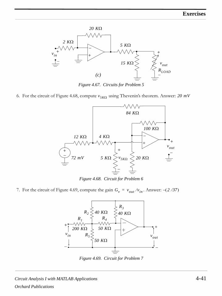
Circuit Analysis I with MATLAB Applications 4-41Orchard Publications
Exercises
Figure 4.67. Circuits for Problem 5
6. For the circuit of Figure 4.68, compute using Thevenin’s theorem. Answer:
Figure 4.68. Circuit for Problem 6
7. For the circuit of Figure 4.69, compute the gain . Answer:
Figure 4.69. Circuit for Problem 7
+
−+
−
−
+
(c)
5 KΩ
vout
2 KΩ
20 KΩ
15 KΩ
RLOAD
vin
v5KΩ 20 mV
+
−
+ −−
+
+
−
vout
72 mV v5KΩ 20 KΩ
12 KΩ
84 KΩ
100 KΩ
5 KΩ
4 KΩ
Gv vout vin⁄= 2 37⁄( ) –
++
−−
voutvin
R2R1
R3
R4
R5
200 KΩ
40 KΩ
50 KΩ
50 KΩ
40 KΩ

Chapter 4 Introduction to Operational Amplifiers
4-42 Circuit Analysis I with MATLAB ApplicationsOrchard Publications
8. For the circuit of Figure 4.70, show that the gain is given by
Figure 4.70. Circuit for Problem 8
Gvvoutvin--------- 1
R1------– R5 R3
R5R4------ 1+⎝ ⎠
⎛ ⎞+= =
++
−−
voutvin
R1
R2
R3 R4R5

Circuit Analysis I with MATLAB Applications 4-43Orchard Publications
Answers to Exercises
4.12 Answers to Exercises
Multiple Choice
1. C For and , the gain must be or . Therefore,
2. A
3. D All current flows through and the voltage drop across it is
4. E All current flows through and the voltage drop across it is . Sincethis circuit is a unity gain amplifier, it follows that also.
5. C . Therefore, .Applying KCL at the plus (+) terminal of we get
6. D The gain of each of the non-inverting op amps is 2. Thus, the output of the first op amp is and the output of the second is .
7. E By superposition, due to acting alone is and due to acting alone is
. Therefore,
8. B We assign node voltage as shown below and we replace the encircled port by its equiva-lent. . Then will be
We now attach the remaining resistors and the entire equivalent circuit is shown below.
vin 2= vout 8= Gv 4= 1 Rf Rin⁄+ 4=
Rf 3 KΩ=
vout Rf Rin⁄ vin×– 9 V–= =
Rf 2 mA 5 KΩ×( )– 10 V–=
R 4 mA 3 KΩ× 12 V=
vout 12 V=
vout 18 12⁄( ) 4×– 6 V–= = iLOAD vout RLOAD⁄ 6 V 6 KΩ⁄– 1 mA–= = =
vout
i 6 V–6 KΩ-------------- 6 V– 4 V–
18 KΩ 12 KΩ+----------------------------------------+ 1– 1
3---–
43--- mA–= = =
2 V 4 V
vout1vin1
2 V– vout2vin2
8 V vout 2– 8+ 6 V= =
vA
vin 30 V= vout
+−
+
−− +vin
10 KΩ
vout
20 KΩ10 KΩ
10 KΩ
10 KΩ vA
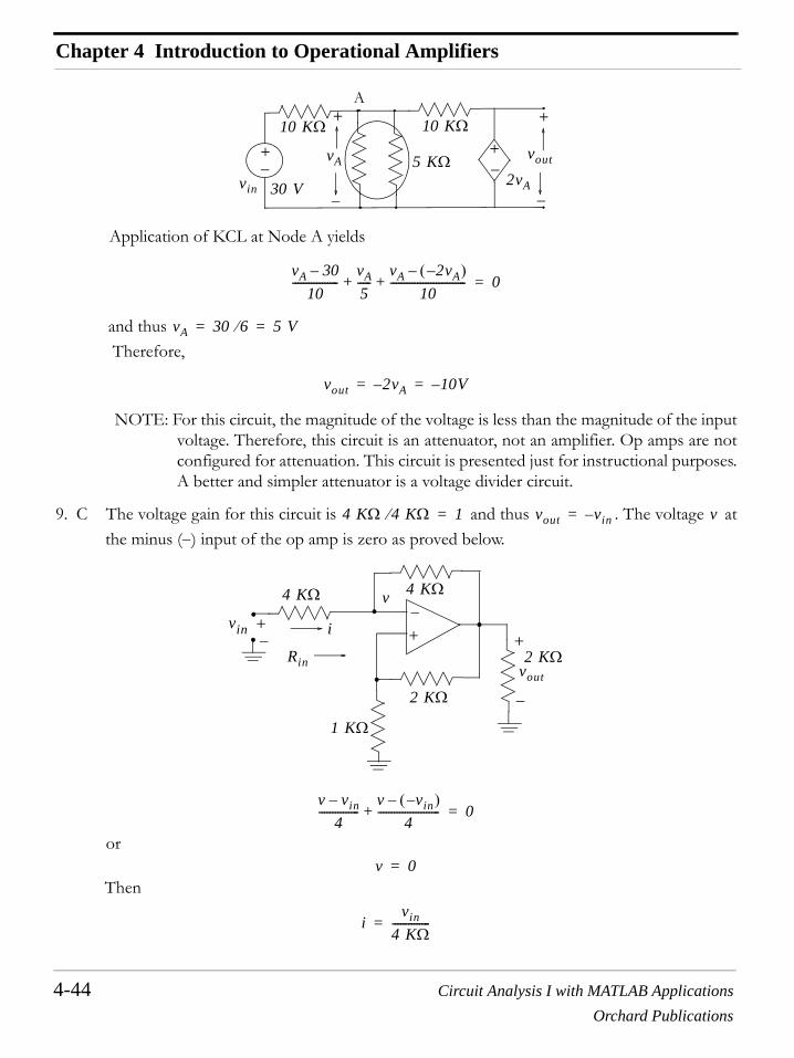
Chapter 4 Introduction to Operational Amplifiers
4-44 Circuit Analysis I with MATLAB ApplicationsOrchard Publications
Application of KCL at Node A yields
and thus Therefore,
NOTE: For this circuit, the magnitude of the voltage is less than the magnitude of the inputvoltage. Therefore, this circuit is an attenuator, not an amplifier. Op amps are notconfigured for attenuation. This circuit is presented just for instructional purposes.A better and simpler attenuator is a voltage divider circuit.
9. C The voltage gain for this circuit is and thus . The voltage atthe minus (−) input of the op amp is zero as proved below.
or
Then
− −+ +
+ +
− −
voutvA
vin 30 V
10 KΩ 10 KΩ
5 KΩ2vA
A
vA 30–
10-----------------
vA5-----
vA 2vA–( )–
10----------------------------+ + 0=
vA 30 6⁄ 5 V= =
vout 2vA– 10V–= =
4 KΩ 4 KΩ⁄ 1= vout vin–= v
+−
+−
vin
4 KΩ
+
−
vout
4 KΩ
2 KΩ
1 KΩ
2 KΩRin
i
v
v vin–
4---------------
v vin–( )–
4-----------------------+ 0=
v 0=
ivin
4 KΩ--------------=

Circuit Analysis I with MATLAB Applications 4-45Orchard Publications
Answers to Exercises
and
10. A For this circuit, and thus . Then,
Problems
1.
and thus
Then
2. We assign , , and as shown below.
and by the voltage division expression
and since this is a unity gain amplifier, we get
Then
Rinvin
vin 4 KΩ⁄------------------------ 4 KΩ= =
vX 10 V–= 40vX 400 V–= i 400 10⁄– 40 A–= =
vout1 27 3⁄( ) 10×– 90 mV–= =
vin2 vout1 90 mV–= =
vout2 1 9010------+⎝ ⎠
⎛ ⎞ 90–( )× 0.9 V–= =
RLOAD v1 vLOAD
+−
60 mV
+
−
3 KΩ
i5KΩ4 KΩ
6 KΩ5 KΩ
v1vLOAD
++
− −
3 KΩ 6 KΩ|| 2 KΩ=
v12 KΩ
4 KΩ 2 KΩ+---------------------------------- 60 mV× 20 mV= =
vLOAD v1 20 mV= =

Chapter 4 Introduction to Operational Amplifiers
4-46 Circuit Analysis I with MATLAB ApplicationsOrchard Publications
3. By superposition
where
We observe that the minus (−) is a virtual ground and thus there is no current flow in and. Also,
and
Then,
4. We assign voltages and as shown below.
i5KΩvLOADRLOAD---------------- 20 mV
5 KΩ---------------- 20 10 3–×
5 103×----------------------- 4 10 6– A× 4 µA= = = = =
vout vout1 vout2 vout3+ +=
vout1 vin2 0=
vin3 0=
RfRin1----------vin1–=
Rin1
Rin2
vout2 vin1 0=
vin3 0=
RfRin2----------vin2–=
vout3 vin1 0=
vin2 0=
RfRin3---------- v– in3( )–=
vout Rfvin3Rin3----------
vin2Rin2----------
vin1Rin1----------––⎝ ⎠
⎛ ⎞=
v− v+
40 mV+−
+
−
+
−
vout
10 KΩ
20 KΩ40 KΩ
50 KΩv−v+

Circuit Analysis I with MATLAB Applications 4-47Orchard Publications
Answers to Exercises
At the minus (−) terminal
or
At the plus (+) terminal
or
or
Since we equate the nodal equations and we get
Multiplication by yields
or
Check with (4.21) using MATLAB:
R1=10000; R2=20000; R3=40000; Rf=50000; Vin=40*10^(−3);Vout=(R1*R3-R2*Rf)*Vin/(R1*(R2+R3))
Vout =
-0.0400
5. We attach the , , and resistors to the equivalent circuit as shown below. ByThevenin’s theorem
v− 40 mV–
10 KΩ----------------------------
v− vout–
50 KΩ---------------------+ 0=
650 103×--------------------v−
150 103×--------------------vout– 4 10 6–×=
v+ 40 mV–
20 KΩ---------------------------
v+40 KΩ-----------------+ 0=
340 10 3×---------------------v+ 2 10 6–×=
v+80 10 3–×
3-----------------------=
v+ v−=
650 103×-------------------- 80 10 3–×
3-----------------------⎝ ⎠
⎛ ⎞ 150 103×--------------------vout– 4 10 6–×=
50 103×
2 80 10 3–×× 50 103××
50 103×----------------------------------------------------------- vout– 4 10 6–× 50 103××=
vout 40 mV–=
5 KΩ 15 KΩ RLOAD

Chapter 4 Introduction to Operational Amplifiers
4-48 Circuit Analysis I with MATLAB ApplicationsOrchard Publications
or
Because the circuit contains a dependent source, we must compute the Thevenin resistance usingthe relation where is found from the circuit below.
We observe that the short circuit shorts out the and thus
Then
and the Thevenin equivalent circuit is shown below.
Therefore, for maximum power transfer we must have
+−+
−2 KΩ
10vinvin
5 KΩ
15 KΩ
×
×
b
a
vTH vOC vab15 KΩ
5 KΩ 15 KΩ+------------------------------------- 10vin–( )= = =
vTH 7.5vin–=
RTH vTH iSC⁄= iSC
+− 10vin
5 KΩ
15 KΩ
×
×
b
a
iSC
15 KΩ
iSC10vin–
5 KΩ---------------- 2 10 3– vin×–= =
RTH7.5vin–
2 10 3– vin×–------------------------------ 3.75 KΩ= =
+−
vTH
RTH 3.75 KΩ=
RLOAD
RLOAD RTH 3.75 KΩ= =
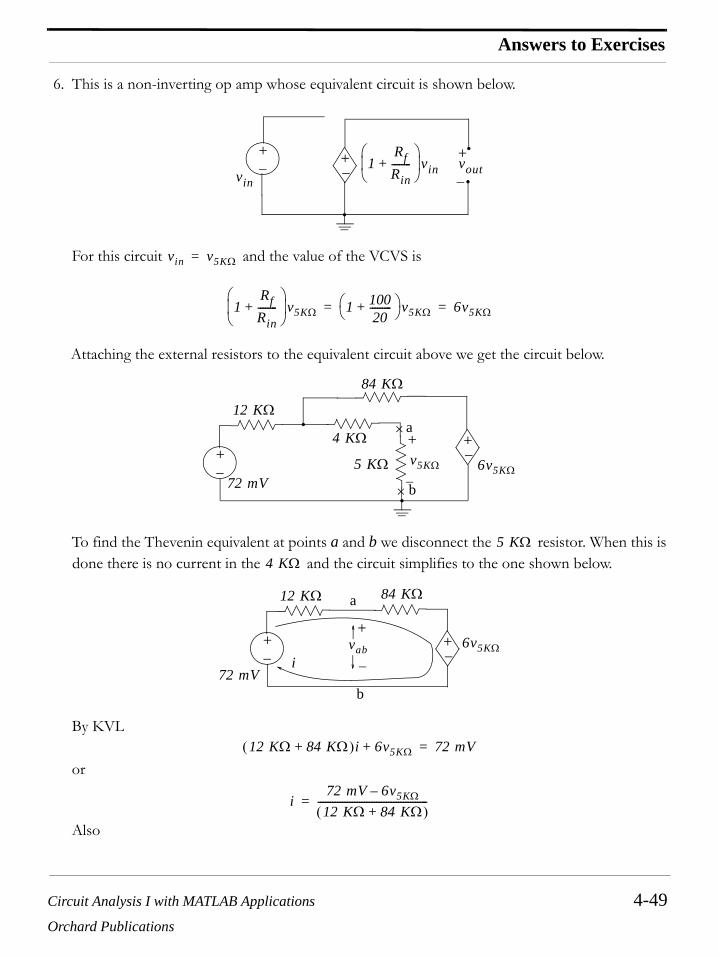
Circuit Analysis I with MATLAB Applications 4-49Orchard Publications
Answers to Exercises
6. This is a non-inverting op amp whose equivalent circuit is shown below.
For this circuit and the value of the VCVS is
Attaching the external resistors to the equivalent circuit above we get the circuit below.
To find the Thevenin equivalent at points a and b we disconnect the resistor. When this isdone there is no current in the and the circuit simplifies to the one shown below.
By KVL
or
Also
+
−−
++−
1RfRin--------+
⎝ ⎠⎜ ⎟⎛ ⎞
vin voutvin
vin v5KΩ=
1RfRin--------+
⎝ ⎠⎜ ⎟⎛ ⎞
v5KΩ 1 10020---------+⎝ ⎠
⎛ ⎞ v5KΩ 6v5KΩ= =
+
−−
+ +−v5KΩ
72 mV
12 KΩ
4 KΩ
84 KΩ
5 KΩ
×
×
a
b
6v5KΩ
5 KΩ4 KΩ
+−
+−
6v5KΩ
72 mV
12 KΩ 84 KΩ
i
a
b
vab
+
−
12 KΩ 84 KΩ+( )i 6v5KΩ+ 72 mV=
i72 mV 6v5KΩ–
12 KΩ 84 KΩ+( )---------------------------------------------=

Chapter 4 Introduction to Operational Amplifiers
4-50 Circuit Analysis I with MATLAB ApplicationsOrchard Publications
or
and thus
The Thevenin resistance is found from where is computed with the termi-nals a and b shorted making and the circuit is as shown on the left below. We also per-form voltage-source to current-source transformation and we get the circuit on the right below.
Now
and by the current division expression
Therefore,
and the Thevenin equivalent circuit with the resistor is shown below.
vTH vab v5KΩ 72 mV 12 KΩ( )i– 72 mV 12 KΩ72 mV 6v5KΩ–
96 KΩ-------------------------------------⎝ ⎠
⎛ ⎞–= = = =
72 mV 9 mV–34---v5KΩ+=
v5KΩ34---v5KΩ– 63 mV=
vTH vab v5KΩ 252 mV= = =
RTH vOC iSC⁄= iSC
v5KΩ 0=
+−72 mV
12 KΩ
84 KΩa
biSC
4 KΩ
6 µA
12 KΩ
84 KΩ a
biSC
4 KΩ
12 KΩ 84 KΩ|| 10.5 KΩ=
iSC iab10.5 KΩ
10.5 KΩ 4 KΩ+------------------------------------------ 6 µA× 126
29--------- µA= = =
RTHvOCiSC--------- 252
126 29⁄------------------- 58 KΩ= = =
5 KΩ
+− 5 KΩ
a
b
RTH 12 KΩ=
vTH 252 mV=

Circuit Analysis I with MATLAB Applications 4-51Orchard Publications
Answers to Exercises
Finally,
7. We assign node voltages and as shown below and we write node equations observing that (virtual ground).
Node 1:
or
Multiplication of each term by and simplification yields
Node 2:
or
Equating the right sides we get
or
v5KΩ5
58 5+--------------- 252× 20 mV= =
v1 v2
v2 0=
++
−−
voutvin
R2R1
R3
R4
R5
200 KΩ
40 KΩ
50 KΩ
50 KΩ
40 KΩv1 v2
v1 vin–
200 KΩ--------------------
v1 vout–
40 KΩ--------------------
v1 0–
50 KΩ-----------------
v150 KΩ-----------------+ + + 0=
1200 KΩ-------------------- 1
40 KΩ----------------- 1
50 KΩ----------------- 1
50 KΩ-----------------+ + +⎝ ⎠
⎛ ⎞ v1vin
200 KΩ--------------------
vout40 KΩ-----------------+=
200 KΩ
v11
14------ vin 5vout+( )=
0 v1–
50 KΩ-----------------
0 vout–
40 KΩ------------------+ 0=
v154---vout–=
114------ vin 5vout+( ) 5
4---vout–=

Chapter 4 Introduction to Operational Amplifiers
4-52 Circuit Analysis I with MATLAB ApplicationsOrchard Publications
Simplifying and dividing both sides by we get
8. We assign node voltages and as shown below and we write node equations observing that (virtual ground).
Node 1:
or
Node 2:
or
or
3728------vout
114------vin–=
vin
Gvvoutvin--------- 2
37------–= =
v1 v2
v1 0=
++
−−
voutvin
R1
R2
R3 R4R5
v1
v2
0 vin–
R1---------------
0 v2–
R3--------------+ 0=
v2R3R1------vin–=
v2 0–
R3--------------
v2R4------
v2 vout–
R5--------------------+ + 0=
1R3------ 1
R4------ 1
R5------+ +⎝ ⎠
⎛ ⎞ v2voutR5
---------=
v21
R5 R3⁄ R5 R4⁄ 1+ +------------------------------------------------vout=

Circuit Analysis I with MATLAB Applications 4-53Orchard Publications
Answers to Exercises
Equating the right sides we get
Simplifying and dividing both sides by we get
1R5 R3⁄ R5 R4⁄ 1+ +------------------------------------------------vout
R3R1------vin–=
vin
Gvvoutvin--------- 1
R1------– R5 R3
R5R4------ 1+⎝ ⎠
⎛ ⎞+= =

Chapter 4 Introduction to Operational Amplifiers
4-54 Circuit Analysis I with MATLAB ApplicationsOrchard Publications
NOTES

Circuit Analysis I with MATLAB Applications 5-1Orchard Publications
Chapter 5
Inductance and Capacitance
his chapter is an introduction to inductance and capacitance, their voltage-current relation-ships, power absorbed, and energy stored in inductors and capacitors. Procedures for analyz-ing circuits with inductors and capacitors are presented along with several examples.
5.1 Energy Storage Devices
In the first four chapters we considered resistive circuits only, that is, circuits with resistors and con-stant voltage and current sources. However, resistance is not the only property that an electric circuitpossesses; in every circuit there are two other properties present and these are the inductance and thecapacitance. We will see through some examples that will be presented later in this chapter, thatinductance and capacitance have an effect on an electric circuit as long as there are changes in thevoltages and currents in the circuit.
The effects of the inductance and capacitance properties can best be stated in simple differentialequations since they involve the changes in voltage or current with time. We will study inductancefirst.
5.2 Inductance
Inductance is associated with the magnetic field which is always present when there is an electric cur-rent. Thus, when current flows in an electric circuit the conductors (wires) connecting the devices inthe circuit are surrounded by a magnetic field. Figure 5.1 shows a simple loop of wire and its mag-netic field represented by the small loops.
Figure 5.1. Magnetic field around a loop of wire
The direction of the magnetic field (not shown) can be determined by the left-hand rule if conven-tional current flow is assumed, or by the right-hand rule if electron current flow is assumed. Themagnetic field loops are circular in form and are referred to as lines of magnetic flux. The unit of mag-netic flux is the weber (Wb).
T

Chapter 5 Inductance and Capacitance
5-2 Circuit Analysis I with MATLAB ApplicationsOrchard Publications
In a loosely wound coil of wire such as the one shown in Figure 5.2, the current through the woundcoil produces a denser magnetic field and many of the magnetic lines link the coil several times.
Figure 5.2. Magnetic field around several loops of wire
The magnetic flux is denoted as and, if there are N turns and we assume that the flux passesthrough each turn, the total flux, denoted as , is called flux linkage. Then,
(5.1)
Now, we define a linear inductor one in which the flux linkage is proportional to the current throughit, that is,
(5.2)
where the constant of proportionality is called inductance in webers per ampere.
We also recall Faraday’s law of electromagnetic induction which states that
(5.3)
and from (5.2) and (5.3),
(5.4)
Alternately, the inductance is defined as the constant which relates the voltage across and the cur-rent through a device called inductor by the relation of (5.4).
The symbol and the voltage-current* designations for the inductor are shown in Figure 5.3.
Figure 5.3. Symbol for inductor
* In the first four chapters we have used the subscript LOAD to denote a voltage across a load, a current througha load, and the resistance of a such load as to avoid confusion with the subscript L which henceforth willdenote inductance. We will continue using the subscript LOAD for any load connected to a circuit.
ϕ ϕλ
λ Nϕ=
λ Li=
L
v dλdt------=
v Ldidt-----=
L
RLOAD
L
+ −vL
iL
Circuit Analysis I with MATLAB Applications 5-3Orchard Publications
Inductance
For an inductor, the voltage-current relationship is
(5.5)
where and have the indicated polarity and direction. Obviously, has a non-zero value onlywhen changes with time.
The unit of inductance is the Henry abbreviated as . Since
(5.6)
we can say that one henry is the inductance in a circuit in which a voltage of one volt is induced by a currentchanging at the rate of one ampere per second.
By separation of the variables we rewrite (5.5) as
(5.7)
and integrating both sides we get:
or
or
(5.8)
where , more often denoted as , is the current flowing through the inductor at some ref-erence time usually taken as , and it is referred to as the initial condition.
We can also express (5.8) as
(5.9)
vL LdiL
dt-------=
vL iL vL
iL
H
LvL
td
diL
------- voltsamperes
ondssec--------------------------------------------= =
diL1L---vLdt=
id Li t0( )
i t( )
∫ 1L--- vLdt
t0
t
∫=
iL t( ) iL t0( )–1L--- vLdt
t0
t
∫=
iL t( )1L--- vLdt
t0
t
∫ iL t0( )+=
iL t0( ) iL 0( )
t 0=
iL t( ) 1L--- vLdt
∞–
t
∫1L--- vLdt
∞–
0
∫1L--- vLdt
0
t
∫+= =

Chapter 5 Inductance and Capacitance
5-4 Circuit Analysis I with MATLAB ApplicationsOrchard Publications
where the first integral on the right side represents the initial condition.
Example 5.1
The current passing through a inductor is shown in Figure 5.4.
a. Compute the flux linkage at
b. Compute and sketch the voltage for the time interval
Figure 5.4. Waveform for Example 5.1
Solution:
a. The flux linkage is directly proportional to the current; then from (5.1) and (5.2)
Therefore, we need to compute the current i at , , , and
For time interval , where is the slope of the straight line segment, andb is the intercept which, by inspection, is . The slope is
and thus
(5.10)
At , (5.10) yields . Then, the flux linkage is
iL t( ) 50 mH
λ t 2 5 9 and 11 ms, , ,=
vL t( ) ∞ t 14 ms< <–
(mA)
0
510
1520
25
−5
−10
−15−20
t (ms)10 126
3 8
14
iL t( )
λ
λ Nϕ Li= =
t 2 ms= t 5 ms= t 9 ms= t 11 ms=
0 t 3 ms< < i mt b+= mi axis– 25 mA m
m 20– 25–3 0–
---------------------- 15–= =
i t 0=3 ms 15– t 25+=
t 2 ms= i 5 mA–=

Circuit Analysis I with MATLAB Applications 5-5Orchard Publications
Inductance
and
(5.11)
For the time interval , where
and thus
To find b we use the fact that at , as seen in Figure 5.4. Then,
from which .
Thus, the straight line equation for the time interval is
(5.12)
and therefore at , , and the flux linkage is
or
(5.13)
Using the same procedure we find that
(5.14)
Also,
(5.15)
and with (5.15),
(5.16)
Likewise,
λ Li 50 10 3–× 5–( )× 10 3–×= =
λ t 2 ms=250 µWb–=
3 t 6 ms< < i mt b+=
m 15 20–( )–3 0–
-------------------------- 353
------= =
i 353
------t b+=
t 3 ms= i 20 mA–=
20–353
------ 3× b+=
b 55–=
3 t 6 ms< <
i t 3 ms=6 ms 35
3------t 55–=
t 5 ms= i 10 3 mA⁄=
λ Li 50 10 3–× 103
------× 10 3–×= =
λ t 5 ms=500
3--------- µWb=
i t 6 ms=8 ms 12.5– t 90+=
i t 8 ms=10 ms 7.5t 70–=
λ t 9 ms= Li 125 µWb–= =

Chapter 5 Inductance and Capacitance
5-6 Circuit Analysis I with MATLAB ApplicationsOrchard Publications
(5.17)
and with (5.17),
(5.18)
b. Since
to compute and sketch the voltage for the time interval , we only need todifferentiate, that is, compute the slope of the straight line segments for this interval. These werefound in part (a) as (5.10), (5.12), (5.14), (5.15), and (5.17). Then,
(5.19)
(5.20)
(5.21)
(5.22)
(5.23)
(5.24)
i t 10 ms=12 ms 2.5– t 30+=
λ t 11 ms= Li 125 µWb= =
vL LdiLdt-------=
vL t( ) ∞ t 14 ms< <–
slope ∞– t 0< < 0=
vL ∞– t 0< <L slope× 0= =
slope 0 t 3 ms< < 15 mA ms⁄– 15 A s⁄–= =
vL 0 t 3 ms< <L slope× 50 10 3–× v
A s⁄---------- 15 A s⁄–( )× 750 mV–= = =
slope 3 t 6 ms< < 35 3⁄ mA ms⁄ 35 3⁄ A s⁄= =
vL 3 t 6 ms< <L slope× 50 10 3–× 35 3⁄( )× 583.3 mV= = =
slope 6 t 8 ms< < 12.5– mA ms⁄ 12.5– A s⁄= =
vL 6 t 8 ms< <L slope× 50 10 3–× 12.5–( )× 625– mV= = =
slope 8 t 10 ms< < 7.5 mA ms⁄ 7.5 A s⁄= =
vL 8 t 10 ms< <L slope× 50 10 3–× 7.5× 375 mV= = =
slope 10 t 12 ms< < 2.5– mA ms⁄ 2.5– A s⁄= =
vL 10 t 12 ms< <L slope× 50 10 3–× 2.5–( )× 125– mV= = =
slope 12 t 14 ms< < 0=

Circuit Analysis I with MATLAB Applications 5-7Orchard Publications
Inductance
(5.25)
We now have all values given by (5.19) through (5.25) to sketch as a function of time. We can do this easily with a spreadsheet such as Excel as shown in Figure 5.5.
Figure 5.5. Voltage waveform for Example 5.1
Example 5.2
The voltage across a inductor is as shown on the waveform of Figure 5.6, and it is given thatthe initial condition is . Compute and sketch the current which flowsthrough this inductor in the interval
Figure 5.6. Waveform for Example 5.2
vL 12 t 14 ms< <L slope× 0= =
vL
t vL(t)-5.000 0-4.950 0-4.900 0-4.850 0-4.800 0-4.750 0-4.700 0-4.650 0-4.600 0-4.550 0-4.500 0
Voltage waveform for Example 5.1
-800
-400
0
400
800
0 2 4 6 8 10 12 14
t (ms)V
olta
ge (m
V)
50 mHiL t0( ) iL 0( ) 25 mA= =
5 t 5 ms< <–
(V)
0
−0.750
t (ms)10 1264 8 14
−0.125
−0.250
−0.375−0.500
−0.625
0.125
0.250 0.375
0.500
0.625
2
vL t( ) 1.75 3⁄
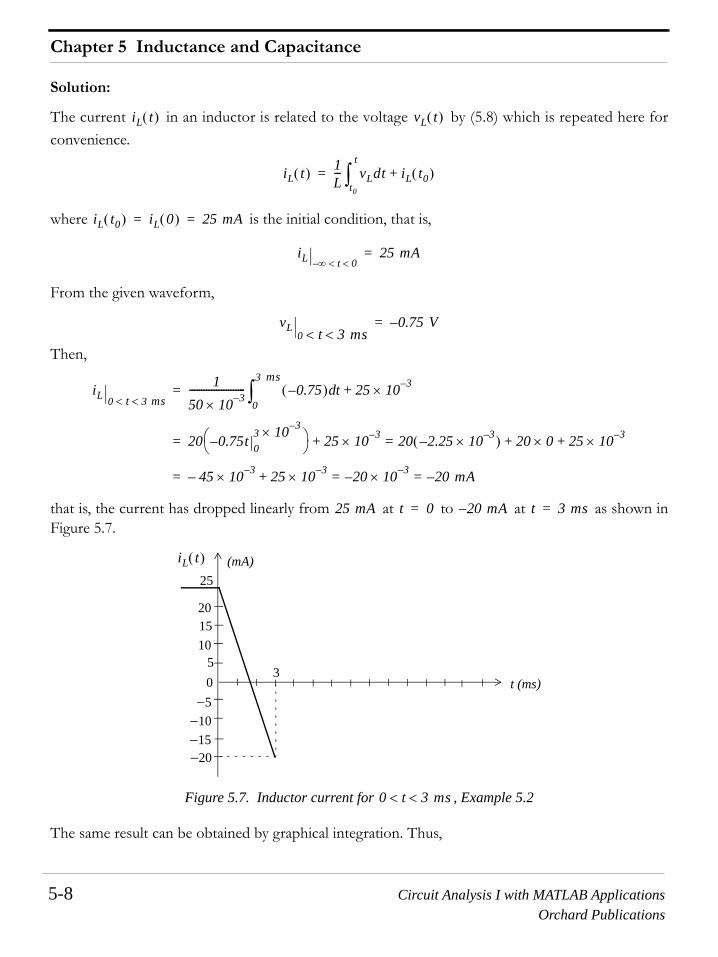
Chapter 5 Inductance and Capacitance
5-8 Circuit Analysis I with MATLAB ApplicationsOrchard Publications
Solution:
The current in an inductor is related to the voltage by (5.8) which is repeated here forconvenience.
where is the initial condition, that is,
From the given waveform,
Then,
that is, the current has dropped linearly from at to at as shown inFigure 5.7.
Figure 5.7. Inductor current for , Example 5.2
The same result can be obtained by graphical integration. Thus,
iL t( ) vL t( )
iL t( ) 1L--- vLdt
t0
t
∫ iL t0( )+=
iL t0( ) iL 0( ) 25 mA= =
iL ∞– t 0< <25 mA=
vL0 t 3 ms< <
0.75 V–=
iL 0 t 3 ms< <
150 10 3–×----------------------- 0.75–( ) td
0
3 ms
∫ 25 10 3–×+=
20 0.75t 03 10 3–×
–⎝ ⎠⎛ ⎞ 25 10 3–×+ 20 2.25 10 3–×–( ) 20 0× 25 10 3–×+ +==
45 10 3–×– 25 10 3–×+ 20– 10 3–× 20 mA–= ==
25 mA t 0= 20 mA– t 3 ms=
(mA)
0
510
1520
25
−5
−10
−15−20
t (ms)3
iL t( )
0 t 3 ms< <

Circuit Analysis I with MATLAB Applications 5-9Orchard Publications
Inductance
and the value of now becomes our initial condition for the time interval
.
Continuing with graphical integration, we get
and now the current has increased linearly from at to at as shown in Figure 5.8.
Figure 5.8. Inductor current for , Example 5.2
For the time interval , we get
Therefore, the current has decreased linearly from at to at asshown in Figure 5.9.
iL t 3 ms=
1L--- Area t 0=
3 ms( ) initial condition+=
20 0.750 3 10 3–××–( ) 25 10 3–×+ 20 mA–==
iL t 3 ms=20 mA–=
3 t 6 ms< <
iL t 6 ms=
1L--- Area t 3=
6 ms( ) initial condition+=
20 1.753
---------- 3 10 3–××⎝ ⎠⎛ ⎞ 20 10 3–×– 15 mA==
20– mA t 3 ms= 15 mA t 6 ms=
(mA)
0
510
1520
25
−5
−10
−15−20
t (ms)6
3
iL t( )
0 t 6 ms<<
6 t 8 ms< <
iL t 8 ms=
1L--- Area t 6=
8 ms( ) initial condition+=
20 0.625– 2 10 3–××( ) 15 10 3–×+ 10– mA==
15 mA t 6 ms= 10– mA t 8 ms=

Chapter 5 Inductance and Capacitance
5-10 Circuit Analysis I with MATLAB ApplicationsOrchard Publications
Figure 5.9. Inductor current for , Example 5.2
For the time interval we get
that is, the current has increased linearly from at to at as shownin Figure 5.10.
Finally, for the time interval we get
that is, the current has decreased linearly from at to at andremains at zero for as shown in Figure 5.11.
(mA)
0
510
1520
25
−5
−10
−15−20
6
3 8t (ms)
iL t( )
0 t 8 ms<<
8 ms t 10 ms<<
iL t 10 ms=
1L--- Area t 8=
10 ms( ) initial condition+=
20 0.375 2 10 3–××( ) 10– 10 3–× 5 mA==
10– mA t 8 ms= 5 mA t 10 ms=
10 ms t 12 ms<<
iL t 12 ms=
1L--- Area t 10=
12 ms( ) initial condition+=
20 0.125– 2 10 3–××( ) 5 10 3–×+ 0==
5 mA t 10 ms= 0 mA t 12 ms=
t 12 ms>
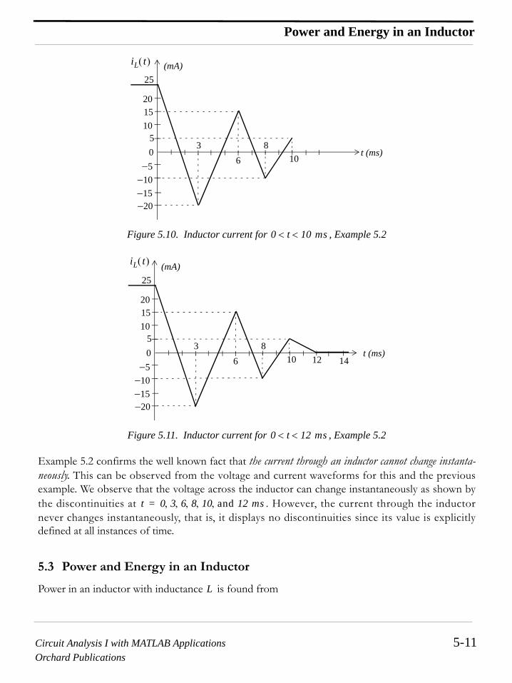
Circuit Analysis I with MATLAB Applications 5-11Orchard Publications
Power and Energy in an Inductor
Figure 5.10. Inductor current for , Example 5.2
Figure 5.11. Inductor current for , Example 5.2
Example 5.2 confirms the well known fact that the current through an inductor cannot change instanta-neously. This can be observed from the voltage and current waveforms for this and the previousexample. We observe that the voltage across the inductor can change instantaneously as shown bythe discontinuities at . However, the current through the inductornever changes instantaneously, that is, it displays no discontinuities since its value is explicitlydefined at all instances of time.
5.3 Power and Energy in an Inductor
Power in an inductor with inductance is found from
(mA)
0
510
1520
25
−5
−10
−15−20
t (ms)106
3 8
iL t( )
0 t 10 ms<<
(mA)
0
510
1520
25
−5
−10
−15−20
t (ms)10 126
3 8
14
iL t( )
0 t 12 ms<<
t 0 3 6 8 10 and 12 ms, , , , ,=
L

Chapter 5 Inductance and Capacitance
5-12 Circuit Analysis I with MATLAB ApplicationsOrchard Publications
(5.26)
and the energy in an inductor, designated as is the integral of the power, that is,
or
or
and letting at , we get the energy stored in an inductor as
(5.27)
Unlike the resistor which dissipates energy (in the form of heat), the (ideal) inductor is a physicaldevice capable of storing energy in analogy to the potential energy of a stretched spring.
Electric circuits that contain inductors can be simplified if the applied voltage and current sourcesare constant as shown by the following example.
Example 5.3
For the circuit shown in Figure 5.12, compute , , and , after steady-state*conditions havebeen reached. Then, compute the power absorbed and the energy consumed by the inductor.
Solution:
Since both the voltage and the current sources are constant, the voltages and the currents in allbranches of the circuit will be constant after steady-state conditions have been reached.
Since
* By steady state conditions we mean the condition (state) where the voltages and currents, after some transient dis-turbances, have subsided. Transients will be in Chapter 10.
pL vLiL L td
diL⎝ ⎠⎛ ⎞ iL LiL td
diL= = =
WL
WL t0
t pL tdt0
t∫ L iL td
diL tdi t0( )
i t( )∫ L iL iLd
i t0( )
i t( )∫= = =
WL t0
t 12---LiL
2
i t0( )
i t( ) 12---L iL
2 t( ) iL2 t0( )–[ ]==
WL t( ) WL t0( )–12---L iL
2 t( ) iL2 t0( )–[ ]=
iL 0= t 0=
WL t( ) 12---LiL
2 t( )=
v1 v2 v3
5 mH
vL LdiL
dt------- L
tdd cons ttan( ) 0= = =

Circuit Analysis I with MATLAB Applications 5-13Orchard Publications
Power and Energy in an Inductor
Figure 5.12. Circuit for Example 5.3
then, all voltages across the inductors will be zero and therefore we can replace all inductors byshort circuits. The given circuit then reduces to the one shown in Figure 5.13 where the and
parallel resistors have been combined into a single resistor.
Figure 5.13. Circuit for Example 5.3 after steady-state conditions have been reached
Now, in Figure 5.13, by inspection, since the resistor was shorted out by the inductor. To find and , let us first find and using nodal analysis.
At Node ,
or
(5.28)
At Node
+−
+ −
+
−
+ −
5 mH
30 mH
40 mH
25 mH
15 mH
20 mH
60 mH
24 V 15 A35 mH
10 Ω
4 Ω 5 Ω
6 Ω3 Ω
8 Ω
12 Ω
v2
v1
v3
9 Ω
3 Ω6 Ω 2 Ω
+−
+ −
+
−
+ −
2 Ω
v1
24 V
4 Ω 9 Ω 5 Ωv2
15 A
v3
8 Ω
vA vB
v1 0= 12 Ω 60 mH
v2 v2 vA vB
vA
vA 24–
4-----------------
vA9-----
vA vB–
5 2+-----------------+ + 0=
14--- 1
9--- 1
7---+ +⎝ ⎠
⎛ ⎞ vA17---vB– 6=
vB
Chapter 5 Inductance and Capacitance
5-14 Circuit Analysis I with MATLAB ApplicationsOrchard Publications
or
(5.29)
We will use the MATLAB code below to find the solution of (5.28) and (5.29).
format rat % Express answers in rational formG=[1/4+1/9+1/7 −1/7; −1/7 1/7+1/8]; I=[6 15]'; V=G\I;disp('vA='); disp(V(1)); disp('vB='); disp(V(2))
vA= 360/11 vB= 808/11
Therefore,
and
that is,
Also,
or
5.4 Combinations of Series and Parallel Inductors
Consider the circuits of figures 5.14 (a) and 5.14 (b) where the source voltage is the same for bothcircuits. We wish to find an expression for the equivalent inductance which we denote as interms of in Figure 5.14 (a) so that the current i will be the same for both circuits.
vB vA–
5 2+----------------- 15–
vB8-----+ 0=
17---vA– 1
7--- 1
8---+⎝ ⎠
⎛ ⎞ vB+ 15=
vA 360 11⁄ V=
vB 808 11⁄ V=
v2 vA v2– 448 11⁄ V–= =
v3 v2 808 11⁄ V= =
p5 mH v5 mH i5 mH× 0 i5 mH× 0= = =
p5 mH 0 watts=
W5 mH12---Li5 mH
2 12---L
v38-----⎝ ⎠
⎛ ⎞2
0.5 5 10 3–×× 808 11⁄8
-------------------⎝ ⎠⎛ ⎞ 2
×= = =
W5 mH 0.211 J=
vS
LSeq
L1 L2 … LN, , ,

Circuit Analysis I with MATLAB Applications 5-15Orchard Publications
Combinations of Series and Parallel Inductors
Figure 5.14. Circuits for derivation of equivalent inductance for inductors in series
From the circuit of Figure 5.14 (a),
or
(5.30)
From the circuit of Figure 5.14 (b),
(5.31)
Equating the left sides of (5.30) and (5.31) we get:
(5.32)
Thus, inductors in series combine as resistors in series do.
Next, we will consider the circuits of Figures 5.15 (a) and 5.15 (b) where the source current is thesame for both circuits. We wish to find an expression for the equivalent inductance which we denoteas in terms of in Figure 5.15 (a) so that the voltage v will be the same for bothcircuits.
Figure 5.15. Circuits for derivation of equivalent inductance for inductors in parallel
From the circuit of Figure 5.15 (a)
+−
+
+
−
++
−
−−
+−ii
(a) (b)
vS L1 L2
LN
vS
LSeq
−
L1didt----- L2
didt----- … LN
didt-----+ + + vS=
L1 L2 … LN+ + +( ) didt----- vS=
LSeqdidt----- vS=
LSeq L1 L2 … LN+ + +=
iS
LPeq L1 L2 … LN, , ,
+
−(a)
+
−(b)
iS
vL1 L2 LN
LPeq
viSi1 iN
i2

Chapter 5 Inductance and Capacitance
5-16 Circuit Analysis I with MATLAB ApplicationsOrchard Publications
or
or
(5.33)
From the circuit of Figure 5.15 (b)
(5.34)
Equating the left sides of (5.33) and (5.34) we get:
(5.35)
and for the special case of two parallel inductors
(5.36)
Thus, inductors in parallel combine as resistors in parallel do.
Example 5.4
For the network of Figure 5.16, replace all inductors by a single equivalent inductor.
Figure 5.16. Network for Example 5.4
i1 i2 … iN+ + + iS=
1L1----- v td
∞–
t∫
1L2----- v td
∞–
t∫ … 1
LN------ v td
∞–
t∫+ + + iS=
1L1----- 1
L2----- … 1
LN------+ + +⎝ ⎠
⎛ ⎞ v td∞–
t∫ iS=
1LPeq----------- v td
∞–
t
∫ iS=
1LPeq----------- 1
L1----- 1
L2----- … 1
LN------+ + +=
LPeq
L1L2
L1 L2+------------------=
120 mH
45 mH
40 mH35 mH
15 mH
30 mH
90 mH
125 mH 60 mHLeq

Circuit Analysis I with MATLAB Applications 5-17Orchard Publications
Capacitance
Solution:
Starting at the right end of the network and moving towards the left end, we find that, , , and a l so
. The network then reduces to that shown in Figure 5.17.
Figure 5.17. First step in combination of inductances
Finally, with reference to Figure 5.17, , and as shown in Figure 5.18.
Figure 5.18. Network showing the equivalent inductance of Figure 5.16
5.5 Capacitance
In Section 5.2 we learned that inductance is associated with a magnetic field which is created when-ever there is current flow. Similarly, capacitance is associated with an electric field. In a simple circuit wecan represent the entire capacitance with a device called capacitor, just as we considered the entireinductance to be concentrated in a single inductor. A capacitor consists of two parallel metal platesseparated by an air space or by a sheet of some type of insulating material called the dielectric.
Now, let us consider the simple series circuit of Figure 5.19 where the device denoted as , is the standard symbol for a capacitor.
Figure 5.19. Simple circuit to illustrate a charged capacitor
60 mH || 120 mH 40 mH= 30 mH || 15 mH 10 mH= 40 mH 35 mH+ 75 mH=
45 mH || 90 mH 30 mH=
30 mH
75 mH
10 mH
125 mH 40 mHLeq
40 mH 35 mH 10 mH+ +( ) || 125 mH 62.5 mH=
Leq 30 mH 62.5 mH+ 92.5 mH= =
92.5 mHLeq
C
+−
C
S
vS
RS

Chapter 5 Inductance and Capacitance
5-18 Circuit Analysis I with MATLAB ApplicationsOrchard Publications
When the switch closes in the circuit of Figure 5.19, the voltage source will force electrons fromits negative terminal through the conductor to the lower plate of the capacitor and it will accumulatenegative charge. At the same time, electrons which were present in the upper plate of the capacitor willmove towards the positive terminal of the voltage source. This action leaves the upper plate of thecapacitor deficient in electrons and thus it becomes positively charged. Therefore, an electric field hasbeen established between the plates of the capacitor.
The distribution of the electric field set up in a capacitor is usually represented by lines of force sim-ilar to the lines of force in a magnetic field. However, in an electric field the lines of force start at thepositive plate and terminate at the negative plate, whereas magnetic lines of force are always com-plete loops.
Figure 5.20 shows the distribution of the electric field between the two plates of a capacitor.
Figure 5.20. Electric field between the plates of a capacitor
We observe that the electric field has an almost uniform density in the area directly between the plates, but it decreases in density beyond the edges of the plates.
The charge on the plates is directly proportional to the voltage between the plates and the capaci-tance is the constant of proportionality. Thus,
(5.37)
and recalling that the current i is the rate of change of the charge q, we have the relation
or
(5.38)
where and in (5.38) obey the passive sign convention.
The unit of capacitance is the Farad abbreviated as F and since
S
+
−
+ ++ ++
− − − − −
qC
q Cv=
i dqdt------
tdd Cv( )= =
iC CdvCdt
---------=
iC vC

Circuit Analysis I with MATLAB Applications 5-19Orchard Publications
Capacitance
(5.39)
we can say that one farad is the capacitance in a circuit in which a current of one ampere flows when the volt-age is changing at the rate of a one volt per second.
By separation of the variables we rewrite (5.38) as
(5.40)
and integrating both sides we get:
or
or
(5.41)
where is the initial condition, that is, the voltage across a capacitor at some reference timeusually taken as , and denoted as .
We can also write (5.41) as
where the initial condition is represented by the first integral on the right side.
Example 5.5
The waveform shown in Figure 5.21 represents the current flowing through a capacitor.Compute and sketch the voltage across this capacitor for the time interval given thatthe initial condition is .
CiC
td
dvC
-------- amperesvolts
ondssec-------------------------------------------= =
dvC1C---- iC dt=
dvCvC t0( )
vC t( )
∫1C---- iCdt
t0
t
∫=
vC t( ) vC t0( )–1C---- iCdt
t0
t
∫=
vC t( ) 1C---- iCdt
t0
t
∫ vC t0( )+=
vC t0( )
t 0= vC 0( )
vC t( ) 1C---- iCdt
∞–
t
∫1C---- iCdt
∞–
0
∫1C---- iCdt
0
t
∫+= =
1 µF0 t 4 ms< <
vC 0( ) 0=

Chapter 5 Inductance and Capacitance
5-20 Circuit Analysis I with MATLAB ApplicationsOrchard Publications
Figure 5.21. Waveform for Example 5.5
Solution:
The initial condition , establishes the first point at the coordinates on the versus time plot of Figure 5.22.
Next,
or
and this value establishes the second point of the straight line segment passing through the origin asshown in Figure 5.22.
Figure 5.22. Straight line segment for of the voltage waveform for Example 5.5
(mA)
0 t (ms)2 3 4
−0.25
−0.50
−0.75−1.00
0.25
0.50 0.75
1.00
1
iC t( )
vC 0( ) 0= 0 0,( ) vC t( )
vC t 1 ms=
1C---- iC td
0
1 10 3–×
∫vC 0( )
0+= ⎧ ⎨ ⎩
vC t 1 ms=
1C---- Area t 0=
1 10 3–×⎝ ⎠⎛ ⎞ 1
1 10 6–×-------------------- 1 10 3–× 1 10 3–××( ) 1 volt= = =
(V)
0t (ms)
2 3 4−0.25
−0.50
−0.75−1.00
0.25 0.50
0.75
1.00
1
vC t( )
0 t 1 ms< <

Circuit Analysis I with MATLAB Applications 5-21Orchard Publications
Capacitance
This value of at becomes our initial condition for the time interval . Con-tinuing, we get
Thus, the capacitor voltage then decreases linearly from at to at as shown in Figure 5.23.
Figure 5.23. Voltage waveform for of Example 5.5
There is no need to calculate the values of the capacitor voltage at and at because the waveform of the current starts repeating itself at , and the initial conditionsand the areas are the same as before. Accordingly, the capacitor voltage waveform of figure (b)starts repeating itself also as shown in Figure 5.24.
Figure 5.24. Voltage waveform for of Example 5.5
1 volt t 1 ms= 1 t 2< <
vC t 2 ms=
1C---- Area t 0=
1 10 3–×⎝ ⎠⎛ ⎞ 1+=
11 10 6–×-------------------- 1– 10 3–× 2 1–( ) 10 3–××( ) 1+ 0 volts==
1 volt t 1 ms= 0 volts t 2 ms=
(V)
0 t (ms)2 3 4−0.25
−0.50
−0.75−1.00
0.25 0.50
0.75
1.00
1
vC t( )
0 t 2 ms< <
vc t 3 ms= t 4 ms=
ic t 2 ms=
vc
(V)
0 t (ms)2 3 4−0.25
−0.50
−0.75−1.00
0.25
0.50 0.75
1.00
1
vC t( )
0 t 4 ms< <

Chapter 5 Inductance and Capacitance
5-22 Circuit Analysis I with MATLAB ApplicationsOrchard Publications
Example 5.5 has illustrated the well known fact that the voltage across a capacitor cannot change instan-taneously. Referring to the current and voltage waveforms for this example, we observe that the cur-rent through the capacitor can change instantaneously as shown by the discontinuities at
in Figure 5.21. However, the voltage across the capacitor never changesinstantaneously, that is, it displays no discontinuities since its value is explicitly defined at all instancesof time as shown in Figure 5.24.
5.6 Power and Energy in a Capacitor
Power in a capacitor with capacitance C is found from
and the energy in a capacitor, denoted as is the integral of the power, that is,
or
and letting at , we get the energy stored in a capacitor as
(5.42)
Like an inductor, a capacitor is a physical device capable of storing energy.
It was stated earlier that the current through an inductor and the voltage across a capacitor cannotchange instantaneously. These facts can also be seen from the expressions of the energy in an induc-tor and in a capacitor, equations (5.27) and (5.42) where we observe that if the current in an inductoror the voltage across a capacitor could change instantaneously, then the energies and wouldalso change instantaneously but this is, of course, a physical impossibility.
Example 5.6
In the circuit of figure 5.25, the voltage and current sources are constant.
t 1 2 3 and 4 ms, , ,=
pC vC iC vC C td
dvC⎝ ⎠⎛ ⎞= =
WC
WC t0
t pC tdt0
t
∫ C vC td
dvC tdv t0( )
v t( )
∫ C vC vcdv t0( )
v t( )
∫= = =
12---Cvc
2
i t0( )
i t( ) 12---C vc
2 t( ) vc2 t0( )–[ ]==
WC t( ) WC t0( )–12---C vc
2 t( ) vc2 t0( )–[ ]=
vC 0= t 0=
WC t( ) 12---CvC
2 t( )=
WL WC

Circuit Analysis I with MATLAB Applications 5-23Orchard Publications
Power and Energy in a Capacitor
a. Compute and
b. Compute the power and energy in the capacitor.
Figure 5.25. Circuit for Example 5.6
Solution:
a. The voltage and current sources are constant; thus, after steady-state conditions have beenreached, the voltages across the inductors will be zero and the currents through the capacitorswill be zero. Therefore, we can replace the inductors by short circuits and the capacitors by opencircuits and the given circuit reduces to that shown in Figure 5.26.
Figure 5.26. First simplification of the circuit of Example 5.6
We can simplify the circuit of figure 5.26 by first exchanging the current source and resistor for a voltage source of in series with as shown in Figure 5.27. We also
combine the series-parallel resistors through . Thus, . But
iL1 vC2
2 µF
+−
+−
30 mH
40 mH
25 mH
20 mH60 mH
24 V
15 AiL1
vC2
10 Ω
4 Ω 2 Ω
5 Ω
7 Ω
6 Ω
8 Ω5 Ω
1 µF3 µF
2 µF
C1
R1
C2
C3
L1
L2
L3
L5L4R5
R6
R8R4
R3
R2 R7
+−
+−24 V
15 AiL1
vC2
10 Ω
4 Ω 2 Ω
5 Ω
7 Ω
6 Ω
8 Ω
R1
R5
R6
R8R4
R3
R2
15 AR8 15 8× 120 V= R8
R1 R4 Req 4 2+( ) || 7 5+( ) 4 Ω= =

Chapter 5 Inductance and Capacitance
5-24 Circuit Analysis I with MATLAB ApplicationsOrchard Publications
now we observe that the branch in which the current flows has disappeared; however, thispresents no problem since we can apply the current division expression once i, shown in Figure5.27, is found. The simplified circuit then is
Figure 5.27. Final simplification of the circuit of Example 5.6
We can apply superposition here. Instead, we will write two mesh equations and we will solve using MATLAB. These in matrix form are
Solution using MATLAB:
format rat; R=[20 −6; −6 14]; V=[24 −120]'; I=R\V; disp(‘i1=’); disp(I(1)); disp(‘i2=’); disp(I(2))
i1= -96/61 i2=
-564/61
Therefore, with reference to the circuit of Figure 5.28
Figure 5.28. Circuit for computation of and for Example 5.6
iL1
+−
+
−24 V
+−
120 V
iReq
4 Ω
R8
8 Ω
6 Ω
R6
R5
10 Ω
i1vC2
i2
20 6–
6– 14i1
i2
24120–
=
+−
+−24 V
15 AiL1
vC2
10 Ω
4 Ω 2 Ω
5 Ω
7 Ω
6 Ω
8 Ω
R1
R5
R6
R8R4
R3
R2
iL1 vC2

Circuit Analysis I with MATLAB Applications 5-25Orchard Publications
Capacitance Combinations
and
b.
and
5.7 Capacitance Combinations
Consider the circuits of figures 5.29 (a) and 5.29 (b) in which the source voltage is the same for both circuits. We want to find an expression for the equivalent capacitance which we denote as in terms of in Figure 5.29 (a) so that the current i will be the same in both circuits.
Figure 5.29. Circuits for derivation of equivalent capacitance for capacitors in series
From the circuit of Figure 5.29 (a),
or
or
(5.43)
From the circuit of Figure 5.29 (b)
iL14 2+( )
4 2+( ) 7 5+( )+---------------------------------------- 96
61------–⎝ ⎠
⎛ ⎞× 3261------– 0.525 A–= = =
vC2 6 9661------– 564
61---------+⎝ ⎠
⎛ ⎞ 280861
------------ 46.03 V= = =
p2 µF v2 µF i2 µF× vC2 0× 0= = =
W2 µF12---Cv2 µF
2 0.5 2 10 6–×× 280861
------------⎝ ⎠⎛ ⎞ 2
× 2 mJ= = =
vS
CSeq
C1 C2 … CN, , ,
+−
+
+
−
+
+−
−−
+−
(a) (b)
vS
i iCSeq
vSC1 C2
CN
vC1 vC2 … vCN+ + + vS=
1C1------ i td
∞–
t
∫1
C2------ i td
∞–
t
∫ … 1CN------- i td
∞–
t
∫+ + + vS=
1C1------ 1
C2------ … 1
CN-------+ + +⎝ ⎠
⎛ ⎞ i td∞–
t
∫ vS=

Chapter 5 Inductance and Capacitance
5-26 Circuit Analysis I with MATLAB ApplicationsOrchard Publications
(5.44)
Equating the left sides of (5.43) and (5.44) we get:
(5.45)
and for the special case of two capacitors in series
(5.46)
Thus capacitors in series combine as resistors in parallel do.
Next, we will consider the circuits of figures 5.30 (a) and 5.30 (b) where the source current is the same for both circuits. We wish to find an expression for the equivalent capacitance which we denote as in terms of in Figure 5.30 (a) so that the voltage will be the same in both circuits.
Figure 5.30. Circuits for derivation of equivalent capacitance for capacitors in parallel
From the circuit of Figure 5.30 (a),
or
or
(5.47)
From the circuit of Figure 5.30 (b),
(5.48)
Equating the left sides of (5.47) and (5.48) we get:
1CSeq----------- i td
∞–
t
∫ vS=
1CSeq----------- 1
C1------ 1
C2------ … 1
CN-------+ + +=
CSeqC1C2
C1 C2+-------------------=
iS
CPeq C1 C2 … CN, , , v
+
−(a)
+
−(b)
iS
vi1 i2 iN
iS
v CPeqCNC2C1
i1 i2 … iN+ + + iS=
C1dvdt------ C2
dvdt------ … CN
dvdt------+ + + iS=
C1 C2 … CN+ + +( ) dvdt------ iS=
CPeqdvdt------ iS=

Circuit Analysis I with MATLAB Applications 5-27Orchard Publications
Capacitance Combinations
(5.49)
Thus, capacitors in parallel combine as resistors in series do.
Example 5.7
For the network of Figure 5.31, replace all capacitors by a single equivalent capacitor.
Figure 5.31. Network for Example 5.7
Solution:
Starting at the right of the network and moving towards the left, we find that ,, , and . The
network then reduces to that shown in Figure 5.32.
Figure 5.32. First step in combination of capacitances
Nex t , t h e s e r i e s comb ina t i on o f y i e l d s and. Finally, the series combination of and yields
as shown in Figure 5.33.
Figure 5.33. Network showing the equivalent inductance of Figure 5.16
CPeq C1 C2 … CN+ + +=
15 µF 30 µF
1 µF 3 µF
8 µF 2 µF
4 µF
56031
--------- µF
12 µF
Ceq
3 µF || 1 µF 4 µF=
2 µF || 4 µF 6 µF= 15 µF in series with 30µF 10µF= 8 µF || 12 µF 20 µF=
10 µF56031
--------- µF6 µF20 µF
4 µF
Ceq
10 4 and 6µF capacitors, , 60 31⁄ µF60 31⁄ µF || 560 31⁄ µF 20 µF= 20 µF 20 µFCeq 10 µF=
20 µFCeq

Chapter 5 Inductance and Capacitance
5-28 Circuit Analysis I with MATLAB ApplicationsOrchard Publications
5.8 Nodal and Mesh Equations in General Terms
In Examples 5.3 and 5.6 the voltage and current sources were constant and therefore, the steady-state circuit analysis could be performed by nodal, mesh or any other method of analysis as welearned in Chapter 3. However, if the voltage and current sources are time-varying quantities wemust apply KCL or KVL in general terms as illustrated by the following example.
Example 5.8
Write nodal and mesh equations for the circuit shown in Figure 5.34.
Figure 5.34. Circuit for Example 5.8
Solution:
Nodal Analysis:
We assign nodes as shown in Figure 5.35. Thus, we need nodal equations.
Figure 5.35. Nodal analysis for the circuit of Example 5.8
At Node 1:
At Node 2:
At Node 3:
+−
+−
CL
vS1 vS2
R1
R2
N 1– 5 1– 4= =
+−
+−
CL
vS1 vS2
R1
R2
v1v2 v3
v0
v4
v1 vS1=
v2 v1–
R1---------------- C d
dt----- v2 v4–( ) 1
L--- v2 v3–( ) td
∞–
t
∫+ + 0=
1L--- v3 v2–( ) td
∞–
t
∫v3R2------+ 0=

Circuit Analysis I with MATLAB Applications 5-29Orchard Publications
Summary
At Node 4:
Mesh Analysis:
We need mesh equations. Thus, we assign currents and asshown in Figure 5.36.
Figure 5.36. Mesh analysis for the circuit of Example 5.8
For Mesh 1:
For Mesh 2:
In both the nodal and mesh equations, the initial conditions are included in the limits of integration.Alternately, we can add the initial condition terms and replace the lower limit of integration withzero in the integrodifferential equations above.
5.9 Summary
• Inductance is associated with a magnetic field which is created whenever there is current flow.
• The magnetic field loops are circular in form and are called lines of magnetic flux. The unit ofmagnetic flux is the weber (Wb).
• The magnetic flux is denoted as and, if there are N turns and we assume that the flux passesthrough each turn, the total flux, denoted as , is called flux linkage. Then,
• For an inductor, the voltage-current relationship is
• The unit of inductance is the Henry abbreviated as H.
• Unlike the resistor which dissipates energy (in the form of heat), the (ideal) inductor is a physicaldevice capable of storing energy in analogy to the potential energy of a stretched spring.
v4 vS2–=
M B 1– 6 5– 1+ 2= = = i1 i2
+−
+−
CL
vS1 vS2
R1
R2i1 i2
R1i11C---- i1 i2–( ) td
∞–
t
∫ vS1 vS2––+ 0=
L ddt-----i2 R2i2 vS2+ +
1C---- i2 i1–( ) td
∞–
t
∫+ 0=
∞–
ϕ ϕ
λ λ Nϕ=
vL L diL dt⁄( )=

Chapter 5 Inductance and Capacitance
5-30 Circuit Analysis I with MATLAB ApplicationsOrchard Publications
• The energy stored in an inductor is
• The current through an inductor cannot change instantaneously.
• In circuits where the applied voltage source or current source are constants, after steady-state con-ditions have been reached, an inductor behaves like a short circuit.
• Inductors in series combine as resistors in series do.
• Inductors in parallel combine as resistors in parallel do.
• Capacitance is associated with an electric field.
• A capacitor consists of two parallel metal plates separated by an air space or by a sheet of sometype of insulating material called the dielectric.
• The charge on the plates of a capacitor is directly proportional to the voltage between the platesand the capacitance is the constant of proportionality. Thus,
• In a capacitor, the voltage-current relationship is
• The unit of capacitance is the Farad abbreviated as F.
• Like an inductor, a capacitor is a physical device capable of storing energy.
• The energy stored in a capacitor is
• The voltage across a capacitor cannot change instantaneously.
• In circuits where the applied voltage source or current source are constants, after steady-state con-ditions have been reached, a capacitor behaves like an open circuit.
• Capacitors in series combine as resistors in parallel do.
• Capacitors in parallel combine as resistors in series do.
• In a circuit that contains inductors and/or capacitors, if the applied voltage and current sourcesare time-varying quantities, the nodal and mesh equations are, in general, integrodifferential equa-tions.
WL t( ) 1 2⁄( )LiL2 t( )=
qC q Cv=
iC C dvC dt⁄( )=
WC t( ) 1 2⁄( )CvC2 t( )=

Circuit Analysis I with MATLAB Applications 5-31Orchard Publications
Exercises
5.10 Exercises
Multiple Choice
1. The unit of inductance is the
A. Farad
B. Ohm
C. mH
D. Weber
E. None of the above
2. The unit of capacitance is the
A.
B. Ohm
C. Farad
D. Coulomb
E. None of the above
3. Faraday’s law of electromagnetic induction states that
A.
B.
C.
D.
E. None of the above
4. In an electric field of a capacitor, the lines of force
A. are complete loops
B. start at the positive plate and end at the negative plate
C. start at the negative plate and end at the positive plate
D. are unpredictable
E. None of the above
µF
λ Nϕ=
λ Li=
v L di dt⁄( )=
v dλ dt⁄=
Chapter 5 Inductance and Capacitance
5-32 Circuit Analysis I with MATLAB ApplicationsOrchard Publications
5. The energy in an inductor is
A.
B.
C.
D. dissipated in the form of heat
E. None of the above
6. The energy in a capacitor is
A.
B.
C.
D. dissipated in the form of heat
E. None of the above
7. In an inductor
A. the voltage cannot change instantaneously
B. the current cannot change instantaneously
C. neither the voltage nor the current can change instantaneously
D. both the voltage and the current can change instantaneously
E. None of the above
8. In a capacitor
A. the voltage cannot change instantaneously
B. the current cannot change instantaneously
C. neither the voltage nor the current can change instantaneously
D. both the voltage and the current can change instantaneously
E. None of the above
9. In the circuit of Figure 5.37 after steady-state conditions have been established, the current through the inductor will be
1 2⁄( ) Li2( )
1 2⁄( ) Lv2( )
vLiL
1 2⁄( ) Ci2( )
1 2⁄( ) Cv2( )
vCiC
iL

Circuit Analysis I with MATLAB Applications 5-33Orchard Publications
Exercises
Figure 5.37. Circuit for Question 9
A.
B.
C.
D.
E. None of the above
10. In the circuit of Figure 5.38 after steady-state conditions have been established, the voltage across the capacitor will be
Figure 5.38. Circuit for Question 10
A.
B.
C.
D.
E. None of the above
Problems
1. The current flowing through a 10 mH inductor is shown by the waveform of Figure 5.39. a. Compute and sketch the voltage across this inductor for b. Compute the first time after when the power absorbed by this inductor is
Answer:
iS
iL
5 A
5 Ω5 mH
0 A
∞ A
2.5 A
5 A
vC
+−
+ −
C
vS
R
10 V
5 Ω2 µF
0 V
∞ V
10– V
10 V
iL
vL t 0>
t 0= pL
pL 50 µw= t 5 ms=

Chapter 5 Inductance and Capacitance
5-34 Circuit Analysis I with MATLAB ApplicationsOrchard Publications
c. Compute the first time after when the power absorbed by this inductor is Answer:
Figure 5.39. Waveform for Problem 1
2. The current flowing through a capacitor is given as , and it isknown that
a. Compute and sketch the voltage across this capacitor for b. Compute the first time after when the power absorbed by this capacitor is
. Answer: c. Compute the first time after when the power absorbed by this capacitor is
. Answer:
3. For the network of Figure 5.40, compute the total energy stored in the series combination of theresistor, capacitor, and inductor at if:
a. and it is known that . Answer:
b. and it is known that . Answer:
Figure 5.40. Network for Problem 3
4. For the circuit of Figure 5.41, compute the energy stored in the inductor at giventhat . Answer:
t 0= pL
pL 50– µw= t 25 ms=
60
50
302010
−10
10
040
(mA)
t (ms)
iL
iC 1 µF iC t( ) 100t mAcos=
vC 0( ) 0=
vC t 0>
t 0= pC
pC 5 mw= 7.85 ms
t 0= pC
pC 5– mw= 23.56 ms
t 10 ms=
i t( ) 0.1e 100t– mA= vC 0( ) 10 V–= 3.4 mJ
i t( ) 0.5 5t cos mA= vC 0( ) 0= 50 µJ
R CL
Rest of the Network
5 Ω 0.4 mH 100 µF
+ −
i t( )
vC t( )
5 mH t 1 s=
i 0( ) 0= 1 mJ

Circuit Analysis I with MATLAB Applications 5-35Orchard Publications
Exercises
Figure 5.41. Circuit for Problem 4
5. For the circuit of Figure 5.42, replace all capacitors with an equivalent capacitance and thencompute the energy stored in at given that in all capacitors.Answer:
Figure 5.42. Circuit for Problem 5
6. Write nodal equations for the circuit of Figure 5.43.
Figure 5.43. Circuit for Problem 6
7. Write mesh equations for the circuit of Figure 5.44.
Figure 5.44. Circuit for Problem 7
+−
5 mH
10 mH 7 mH
3 mH
vS t( )
i t( )
10e t– mV
Ceq
Ceq t 1 ms= vC 0( ) 0=
10 pJ
6 µF
3 µF
8 µF
10 µF
10 µAiS t( )
+−
R1
C1
L
R2
C2vS t( )
+−
R1
L2
R2
L1C1
C2
vS t( )

Chapter 5 Inductance and Capacitance
5-36 Circuit Analysis I with MATLAB ApplicationsOrchard Publications
5.11 Answers to Exercises
Multiple Choice
1. E Henry
2. C
3. D
4. B
5. A
6. B
7. B
8. A
9. E
10. D
Problems
1. a. In an inductor the voltage and current are related by . Thus, we
need to compute the slope of each segment of the given waveform and multiply it by .
Likewise,
The current, voltage, and power waveforms are shown below.
5 A–
vL L diL dt⁄( ) L slope×= =
L
vL 0
10 ms L slope× L∆iL∆t-------- 10 10 3–× 10 10 3– A×
10 10 3– s×----------------------------× 10 mV= = = =
vL 10
20 ms L slope× L 0× 0 mV= = =
vL 20
40 ms L slope× 10 10 3–× 10– 10( )–[ ] 10 3– A×
40 20–( ) 10 3– s×---------------------------------------------------× 10– mV= = =
vL 4050 ms L slope× L 0× 0 mV= = =
vL 010 ms L slope× 10 10 3–× 0 10–( )–[ ] 10 3– A×
60 50–( ) 10 3– s×--------------------------------------------------× 10 mV= = =

Circuit Analysis I with MATLAB Applications 5-37Orchard Publications
Answers to Exercises
b. From the power waveform above, we observe that occurs for the firsttime at point A where
c. From the power waveform above, we observe that occurs for the firsttime at point A where
2. a. For this problem and the current is a sinusoid given as as shown below. The voltage across this capacitor is found from
60
50
302010
−10
10
040
(mA)
t (ms)
iL
10 mH
iL t( )
+ −
vL t( ) 6050302010
−10
10
0 40
(mV)
t (ms)
vL
60503020
10
−100
100
0 40 t (ms)
pL µ w( )
pL vLiL=
A
B
pL vLiL 50 µw= =
t 5 ms=
pL vLiL 50– µw= =
t 25 ms=
C 1 µF 10 6– F= = iC
iC t( ) 100t mAcos= vC t( )
vC t( ) 1C---- iC τd
0
t
∫ vC 0( )+ 106 10 3–( ) 100τcos τ 0+d0
t
∫= =
103 100τcos τd0
t
∫103
100--------- 100τsin
0
t
10 100tsin= ==

Chapter 5 Inductance and Capacitance
5-38 Circuit Analysis I with MATLAB ApplicationsOrchard Publications
and the waveform of is shown below.
Now, or . Then, or and
or
b. Since is a sine function and a cosine function, the first time after zero that theirproduct will be positive is in the interval where we want or
or
Recalling that
iC t( )
t s( )
mA( ) 100tcos
vC t( )
10 100tsin10
10–
vC t( )V( )
π50------π
100---------
T
ωT 2π= ω 2π T⁄= 10 2πT
------tsin 10 100tsin= 2π T⁄ 100=
T 2π 100⁄= T π 50⁄=
vC t( ) iC t( )
0 t π 200⁄< < pC vCiC 5 mw= =
pC 10 100tsin( ) 10 3– 100tcos( ) 5 10 3– w×= =
pC 10 100tsin( ) 100tcos( ) 5 w= =

Circuit Analysis I with MATLAB Applications 5-39Orchard Publications
Answers to Exercises
it follows that
or
or
c. The time where will occur for the first time is after orafter . Therefore, will occur for the first time at
3. a. There is no energy stored in the resistor; it is dissipated in the form of heat. Thus, the totalenergy is stored in the capacitor and the inductor, that is,
where
and
or
Then,
We’ve used MATLAB as a calculator to obtain the answer, that is,
WT=2.5*10^(−4)*((0.1*exp(−1))^2+((−10)*exp(−1))^2);fprintf(' \n'); fprintf('WT=%7.4f J',WT); fprintf(' \n')
WT= 0.0034 J
b. For this part
2xsin 2 x xcossin=
pC 5 200tsin 5 w= =
200tsin 1=
t 11–sin200
--------------- π 2⁄200---------- π
400--------- 0.00785 s 7.85 ms= = = = =
pC 5 mw–= 7.85 ms t π 200⁄ s=
t 1000π 200⁄ ms 5π ms= = pC 5 mw–=
t 7.85 5π+ 7.85 15.71+ 23.56 ms= = =
WT WL WC+12---LiL
2 12---CvC
2+= =
iL i t( ) 0.1e 100t–= =
vC t( ) 1C---- iC τd
0
t
∫ vC 0( )+ 104 0.1e 100τ– τ 10–d0
t
∫= =
104 0.1×100–
----------------------e 100τ–
0
t
10– 10e 100τ–t
010 10e 100t–– 10–= ==
vC t( ) 10e 100t––=
WT t 10 ms=
12--- 0.4 10 3–×× 0.1e 100t–( )
2× 1
2--- 10 4–× 10e 100t––( )
2×+=
2.5 10 4– 0.1e 1–( )2
10e 1––( )2
+[ ]× 3.4 mJ==
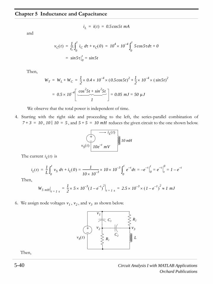
Chapter 5 Inductance and Capacitance
5-40 Circuit Analysis I with MATLAB ApplicationsOrchard Publications
and
Then,
We observe that the total power is independent of time.
4. Starting with the right side and proceeding to the left, the series-parallel combination of, , and reduces the given circuit to the one shown below.
The current is
Then,
6. We assign node voltages , , and as shown below.
Then,
iL i t( ) 0.5 5t mAcos= =
vC t( ) 1C---- iC τd
0
t
∫ vC 0( )+ 104 10 4–× 5 5τ τ 0+dcos0
t
∫= =
5τsin 0t 5tsin==
WT WL WC+12--- 0.4 10 4–×× 0.5 5tcos( )2× 1
2--- 10 4–× 5tsin( )2×+= =
0.5 10 4– 52cos t 52 tsin+
1× 0.05 mJ 50 µJ= == ⎧ ⎪ ⎪ ⎨ ⎪ ⎪ ⎩
7 3+ 10= 10 10|| 5= 5 5+ 10 mH=
+− 10 mH
vS t( )
iL t( )
10e t– mV
iL t( )
iL t( )1L--- vS τd
0
t
∫ iL 0( )+1
10 10 3–×----------------------- 10 10 3–×× e τ– τd
0
t
∫ e τ–– 0
te τ–
t
01 e t––= = = ==
W5 mH t 1 s=
12--- 5 10 3–×× 1 e t––( )
2t 1 s=
2.5 10 3– 1 e 1––( )2
×× 1 mJ≈= =
v1 v2 v3
+−
R1
C1
L
R2
C2vS t( )
v1
v2 v3

Circuit Analysis I with MATLAB Applications 5-41Orchard Publications
Answers to Exercises
7. We assign mesh currents , , and as shown below.
Then,
v1 vS=
C1ddt----- v2 v1–( ) C2
ddt----- v2 v3–( )
v2R1------+ + 0=
v3 v1–
R2---------------- C2
ddt----- v3 v2–( ) 1
L--- v3 τd
∞–
t
∫+ + 0=
i1 i2 i3
+−
R1
L2
R2
L1
C1
C2
vS t( ) i1
i2
i3
1C1------ i1 τd
∞–
t
∫ R1 i1 i2–( ) 1C2------ i1 i3–( ) τd
∞–
t
∫+ + vS=
R1 i2 i1–( ) L1di2dt------- L2
ddt----- i2 i3–( )+ + 0=
1C2------ i3 i1–( ) τd
∞–
t
∫ L2ddt----- i3 i2–( ) R2i3+ + 0=
Chapter 5 Inductance and Capacitance
5-42 Circuit Analysis I with MATLAB ApplicationsOrchard Publications
NOTES

Circuit Analysis I with MATLAB Applications 6-1Orchard Publications
Chapter 6
Sinusoidal Circuit Analysis
his chapter is an introduction to circuits in which the applied voltage or current are sinusoidal.The time and frequency domains are defined and phasor relationships are developed for resis-tive, inductive and capacitive circuits. Reactance, susceptance, impedance and admittance are
also defined. It is assumed that the reader is familiar with sinusoids and complex numbers. If not, itis strongly recommended that Appendix B is reviewed thoroughly before reading this chapter.
6.1 Excitation Functions
The applied voltages and currents in electric circuits are generally referred to as excitations or drivingfunctions, that is, we say that a circuit is “excited” or “driven” by a constant, or a sinusoidal, or anexponential function of time. Another term used in circuit analysis is the word response; this may bethe voltage or current in the “load” part of the circuit or any other part of it. Thus the response maybe anything we define it as a response. Generally, the response is the voltage or current at the outputof a circuit, but we need to specify what the output of a circuit is.
In Chapters 1 through 4 we considered circuits that consisted of excitations (active sources) andresistors only as the passive devices. We used various methods such as nodal and mesh analyses,superposition, Thevenin’s and Norton’s theorems to find the desired response such as the voltageand/or current in any particular branch. The circuit analysis procedure for these circuits is the samefor DC and AC circuits. Thus, if the excitation is a constant voltage or current, the response will alsobe some constant value; if the excitation is a sinusoidal voltage or current, the response will also besinusoidal with the same frequency but different amplitude and phase.
In Chapter 5 we learned that when the excitation is a constant and steady-state conditions arereached, an inductor behaves like a short circuit and a capacitor behaves like an open circuit. How-ever, when the excitation is a time-varying function such as a sinusoid, inductors and capacitorsbehave entirely different as we will see in our subsequent discussion.
6.2 Circuit Response to Sinusoidal Inputs
We can apply the circuit analysis methods which we have learned in previous chapters to circuitswhere the voltage or current sources are sinusoidal. To find out how easy (or how difficult) the pro-cedure becomes, we will consider the simple series circuit of Example 6.1.
Example 6.1
For the circuit shown in Figure 6.1, derive an expression for in terms of , , , and where the subscript p is used to denote the peak or maximum value of a time varying function, and the
T
vC t( ) Vp R C ω

Chapter 6 Sinusoidal Circuit Analysis
6-2 Circuit Analysis I with MATLAB ApplicationsOrchard Publications
sine symbol inside the circle denotes that the excitation is a sinusoidal function.
Figure 6.1. Circuit for Example 6.1
Solution:
By KVL,
(6.1)
where
and
Then,
and by substitution into (6.1) we get
(6.2)
As we know, differentiation (and integration) of a sinusoid of radian frequency results in anothersinusoid of the same frequency . Accordingly, the solution of (6.2) must have the form
(6.3)
where the amplitude and phase angle are constants to be determined from the circuit parame-ters of , , , and . Substitution of (6.3) into (6.2) yields
(6.4)
and recalling that
and
C
R
+−
vS Vp ωtcos=vC t( )i t( )
vR vC+ vS=
vR Ri RiC= =
iC CdvCdt
---------=
vR RCdvCdt
---------=
RCdvCdt
--------- vC+ vS= Vp ωtcos=
ωω
vC t( ) A ωt θ+( )cos=
A θVp R C ω
AωRC ωt θ+( ) A ωt θ+( )cos+sin– Vp ωtcos=
x y+( )sin x ycossin x ysincos+=
x y+( )cos x ycoscos x ysinsin–=
Circuit Analysis I with MATLAB Applications 6-3Orchard Publications
The Complex Excitation Function
we rewrite (6.4) as
Collecting sine and cosine terms, equating like terms and, after some more tedious work, solving foramplitude and phase angle we get:
(6.5)
Obviously, analyzing circuits with sinusoidal excitations when they contain capacitors and/or induc-tors, using the above procedure is impractical. We will see on the next section that the complex excita-tion function greatly simplifies the procedure of analyzing such circuits. Complex numbers are dis-cussed in Appendix B.
The complex excitation function does not imply complexity of a circuit; it just entails the use ofcomplex numbers. We should remember also that when we say that the imaginary part of a complexnumber is some value, there is nothing “imaginary” about this value. In other words, the imaginarypart is just as “real” as the real part of the complex number but it is defined on a different axis. Thuswe display the real part of a complex function on the axis of the reals (usually the x-axis), and theimaginary part on the imaginary axis or the y-axis.
6.3 The Complex Excitation Function
We recall that the derivatives and integrals of sinusoids always produce sinusoids of the same frequencybut different amplitude and phase since the cosine and sine functions are 90 degrees out-of-phase.Thus, if
then
and if
then
Let us consider the network of Figure 6.2 which consists of resistors, inductors and capacitors, andit is driven (excited) by a sinusoidal voltage source .
AωRC ωt θcossin– AωRC ωt θsincos– A ωt θcoscos A ωt θsinsin–+ Vp ωtcos=
A θ
vC t( )Vp
1 ωRC( )2+--------------------------------- ωt tan 1– ωRC( )–( )cos=
v t( ) A ωt θ+( )cos=
tddv ωA ωt θ+( )sin–=
i t( ) B ωt φ+( )sin=
tddi ωB ωt φ+( )cos=
vS t( )

Chapter 6 Sinusoidal Circuit Analysis
6-4 Circuit Analysis I with MATLAB ApplicationsOrchard Publications
Figure 6.2. General presentation of a network showing excitation and load
Let us also define the voltage across the load as * as the response. As we know from Chap-ter 5, the nodal and mesh equations for such circuits are integrodifferential equations, and it is shownin differential equations textbooks† that the forced response or particular solution of these circuits have theform
We also know from Euler’s identity that
(6.6)
and therefore, the real component is the response due to and the imaginary component is theresponse to We will use Example 6.2 to illustrate the ease by which we can obtain theresponse of a circuit, which is excited by a sinusoidal source, using the complex function
approach. In this text, we will represent all sinusoidal variations in terms of the cosine func-tion.
Example 6.2
Repeat Example 6.1, that is, find the capacitor voltage for the circuit of Figure 6.3 using thecomplex excitation method.
Figure 6.3. Circuit for Example 6.2
* Some textbooks denote the voltage across and the current through the load as and respectively. As we statedpreviously, in this text, we use the and notations to avoid confusion with the voltage across andthe current through an inductor.
† This topic is also discussed in Circuit Analysis II with MATLAB® Applications by this author
+
−
LO
AD
Linear NetworkConsisting of
Resistors,Inductors and
Capacitors
Excitation
vS t( )vLOAD t( )
iLOAD t( )
vLOAD t( )
vL iLvLOAD iLOAD vL
iL
vLD t( ) A ωt( )cos B ωt( )sin+=
A ωtcos jA ωtsin+ Ae jωt=
ωtcosωtsin
Ae jωt
vC t( )
C
R
+−
vS Vp ωtcos=vC t( )i t( )
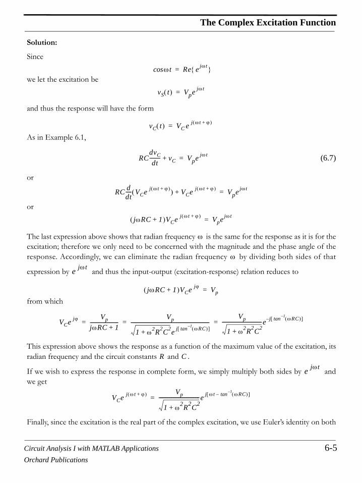
Circuit Analysis I with MATLAB Applications 6-5Orchard Publications
The Complex Excitation Function
Solution:
Since
we let the excitation be
and thus the response will have the form
As in Example 6.1,
(6.7)
or
or
The last expression above shows that radian frequency is the same for the response as it is for theexcitation; therefore we only need to be concerned with the magnitude and the phase angle of theresponse. Accordingly, we can eliminate the radian frequency by dividing both sides of that
expression by and thus the input-output (excitation-response) relation reduces to
from which
This expression above shows the response as a function of the maximum value of the excitation, itsradian frequency and the circuit constants and .
If we wish to express the response in complete form, we simply multiply both sides by andwe get
Finally, since the excitation is the real part of the complex excitation, we use Euler’s identity on both
ωtcos Re e jωt =
vS t( ) Vpe jωt=
vC t( ) VC e j ωt ϕ+( )=
RCdvCdt
--------- vC+ Vpe jωt=
RC ddt----- VCe j ωt ϕ+( )( ) VCe j ωt ϕ+( )+ Vpe jωt=
jωRC 1+( )VCe j ωt ϕ+( ) Vpe jωt=
ω
ω
e jωt
jωRC 1+( )VCe jϕ Vp=
VCe jϕ VpjωRC 1+-----------------------
Vp
1 ω2+ R2C2e j ωRC( )1–tan[ ]----------------------------------------------------------------
Vp
1 ω2+ R2C2--------------------------------e j– ωRC( )1–tan[ ]= = =
R C
e jωt
VCe j ωt ϕ+( ) Vp
1 ω2+ R2C2---------------------------------e j ωt ωRC( )1–tan–[ ]=

Chapter 6 Sinusoidal Circuit Analysis
6-6 Circuit Analysis I with MATLAB ApplicationsOrchard Publications
sides and equating reals parts, we get
The first part of the above procedure where the excitation-response relation is simplified to ampli-tude and phase relationship is known as time-domain to frequency-domain transformation; the second partwhere the excitation-response is put back to its sinusoidal form is known as frequency-domain to time-domain transformation. For brevity, we will denote the time domain as the , and the fre-quency domain as the .
If a sinusoid is given in terms of the sine function, we must first convert it to a cosine function.Thus,
(6.8)
and in the it is expressed as
(6.9)
where represents a phasor (rotating vector) voltage or current .
In summary, the , to transformation procedure is as follows:
1. Express the given sinusoid as a cosine function
2. Express the cosine function as the real part of the complex excitation using Euler’s identity
3. Extract the magnitude and phase angle from it.
Example 6.3
Transform the sinusoid to its equivalent expression.
Solution:
For this example, we have
or
vC t( ) VC ωt φ+( )cosVp
1 ω2+ R2C2
-------------------------------- ωt ωRC( )1–tan–[ ]cos= =
t domain–
jω domain–
m t( ) A ωt θ+( )sin A ωt θ 90°–+( )cos= =
jω domain–
M Ae j θ 90°–( ) A θ 90°–( )∠= =
M V I∗
t domain– jω domain–
v t( ) 10 100t 60°–( )sin= jω domain–
v t( ) 10 100t 60°–( )sin 10 100t 60°– 90°–( )cos= =
v t( ) 10 100t 150°–( )cos= Re 10e j 100t 150°–( )
⎩ ⎭⎨ ⎬⎧ ⎫
=

Circuit Analysis I with MATLAB Applications 6-7Orchard Publications
The Complex Excitation Function
Since the contains only the amplitude and phase, we extract these from the bracketedterm on the right side of the above expression, and we get the phasor as
The to transformation procedure is as follows:
1. Convert the given phasor from polar to exponential form
2. Add the radian frequency multiplied by to the exponential form
3. Extract the real part from it.
Example 6.4
Transform the phasor to its equivalent time-domain expression.
Solution:
First, we express the given phasor in exponential form, that is,
Next, adding the radian frequency multiplied by to the exponent of the above expression weget
and finally we extract the real part from it. Then,
We can add, subtract, multiply and divide sinusoids of the same frequency using phasors as illus-trated by the following example.
Example 6.5
It is given that and . Compute the sum.
jω domain–
V
V 10e j150–°
10 150°–∠= =
jω domain– t domain–
ω t
I 120 90°–∠=
I 120 90°–∠ 120e j90–°
= =
ω t
i t( ) 120e j ωt 90°–( )
=
i t( ) Re 120e j ωt 90°–( )
⎩ ⎭⎨ ⎬⎧ ⎫
120 ωt 90°–( )cos 120 ωtsin= = =
i1 t( ) 10 120πt 45°+( )cos= i2 t( ) 5 120πt 45– °( )sin=
i t( ) i1 t( ) i2 t( )+=

Chapter 6 Sinusoidal Circuit Analysis
6-8 Circuit Analysis I with MATLAB ApplicationsOrchard Publications
Solution:
As a first step, we express as a cosine function, that is,
Next, we perform the to transformation and we obtain the phasors
and by addition,
or
and finally transforming the phasor I into the , we get
Also, for brevity, in our subsequent discussion we will designate resistive, inductive and capacitivecircuits as , , and respectively.
6.4 Phasors in R, L, and C Circuits
The circuit analysis of circuits containing , , and devices, and which are excited by sinusoidalsources, is considerably simplified with the use of phasor voltages and phasor currents which we willrepresent by the boldface capital letters and respectively. We will now derive and phasorrelationships in the . We must always remember that phasor quantities exist onlyin the .
1. and phasor relationship in branches
Consider circuit 6.4 (a) below where the load is purely resistive. We know from Ohm’s law that where the resistance R is a constant. We will show that this relationship also holds
for the phasors and shown in circuit 6.4 (b), that is, we will prove that
Proof:
In circuit 6.4 (a) we let be a complex voltage, that is,
i2 t( )
i2 t( ) 5 120πt 45– °( )sin 5 120πt 45– ° 90°–( )cos 5 120πt 135– °( )cos= = =
t domain– jω domain–
I1 10 45°∠= and I2 5 135– °∠=
I I1 I2+ 10 45°∠ 5 135– °∠+ 10 22
------- j 22
-------+⎝ ⎠⎛ ⎞ 5 2
2-------– j 2
2-------–⎝ ⎠
⎛ ⎞+= = =
I 5 22
------- j 22
-------+⎝ ⎠⎛ ⎞ 5 45°∠= =
t domain–
i t( ) 5 120πt 45°+( )cos=
R L C
R L C
V I V Ijω domain–
jω domain–
V I R
vR t( ) RiR t( )=
VR IR
VR RIR=
vR t( )

Circuit Analysis I with MATLAB Applications 6-9Orchard Publications
Phasors in R, L, and C Circuits
Figure 6.4. Voltage across a resistive load in and
(6.10)
and since is a constant, it will produce a current of the same frequency and the same phase *
whose form will be
and by Ohm’s law,
(6.11)
Transforming (6.11) to the , we obtain the phasor relationship
Since the phasor current is in-phase with the voltage (both and have the same phase ), welet
and it follows that
(6.12)
Therefore, the phasor and relationship in resistors, obeys Ohm’s law also, and the currentthrough a resistor is always in−phase with the voltage across that resistor.
Example 6.6
For the network of Figure 6.5, find when .
* The phase will be the same since neither differentiation nor integration is performed here.
+
−
+
−
vS t( )vR t( )
vR t( ) RiR t( ) Vp ωt θ+( )cos= =
iR t( )
a( ) t domain network– b( ) jω domain phasor( ) network–
VR RIR=
VS
VRIR
t domain– jω domain–
Vpe j ωt φ+( ) Vp ωt φ+( )cos jVp ωt φ+( )sin+=
R ω φ
Ipe j ωt φ+( ) Ip ωt φ+( )cos jIp ωt φ+( )sin+=
Vpe j ωt φ+( ) RIpe j ωt φ+( )=
jω domain–
Vpe jφ RIpe jφ= or Vp φ∠ RIp φ∠=
I V I V φ
Vp φ∠ VR= and Ip φ∠ IR=
VR RIR=
V I
iR t( ) vR t( ) 40 377t 75°–( )sin=
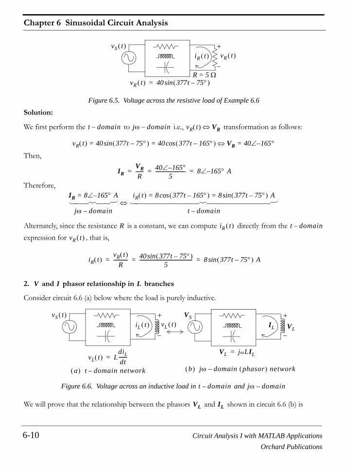
Chapter 6 Sinusoidal Circuit Analysis
6-10 Circuit Analysis I with MATLAB ApplicationsOrchard Publications
Figure 6.5. Voltage across the resistive load of Example 6.6
Solution:
We first perform the to i.e., transformation as follows:
Then,
Therefore,
Alternately, since the resistance is a constant, we can compute directly from the expression for , that is,
2. and phasor relationship in branches
Consider circuit 6.6 (a) below where the load is purely inductive.
Figure 6.6. Voltage across an inductive load in and
We will prove that the relationship between the phasors and shown in circuit 6.6 (b) is
+
−
vS t( )vR t( )
vR t( ) 40 377t 75°–( )sin=
iR t( )
R = 5 Ω
t domain– jω domain– vR t( ) VR⇔
vR t( ) 40 377t 75°–( )sin 40 377t 165°–( )cos= = VR 40 165°–∠=⇔
IRVRR
------- 40 165°–∠5
------------------------- 8 165° A–∠= = =
IR 8 165° A–∠=
jω domain–
iR t( ) 8 377t 165°–( )cos 8 377t 75°–( ) Asin= =
t domain–⇔⎧ ⎪ ⎪ ⎨ ⎪ ⎪ ⎩ ⎧ ⎪ ⎪ ⎪ ⎪ ⎪ ⎪ ⎪ ⎪ ⎪ ⎨ ⎪ ⎪ ⎪ ⎪ ⎪ ⎪ ⎪ ⎪ ⎪ ⎩
R iR t( ) t domain–
vR t( )
iR t( )vR t( )
R------------ 40 377t 75°–( )sin
5-------------------------------------------- 8 377t 75°–( ) Asin= = =
V I L
+
−
+
−
vS t( )vL t( )iL t( )
a( ) t domain network– b( ) jω domain phasor( ) network–
VL jωLIL=
VS
VLIL
vL t( ) LdiLdt-------=
t domain– jω domain–
VL IL

Circuit Analysis I with MATLAB Applications 6-11Orchard Publications
Phasors in R, L, and C Circuits
(6.13)
Proof:
In circuit 6.6 (a) we let be a complex voltage, that is,
(6.14)
and recalling that if , that is, differentiation (or inte-gration) does not change the radian frequency or the phase angle , the current through theinductor will have the form
(6.15)
and since
then,
(6.16)
Next, transforming (6.16) to the , we obtain the phasor relationship
and letting
we get
(6.17)
The presence of the operator in (6.17) indicates that the voltage across an inductor leads the cur-rent through it by .
Example 6.7
For the network of Figure 6.7, find when .
Solution:
We first perform the to i.e., transformation as follows:
VL jωLIL=
vL t( )
Vpe j ωt φ+( ) Vp ωt φ+( )cos jVp ωt φ+( )sin+=
x t( ) ωt φ+( )sin= then dx dt⁄ ω ωt φ+( )cos=
ω φ
Ipe j ωt φ+( ) Ip ωt φ+( )cos jIp ωt φ+( )sin+=
vL t( ) LdiLdt-------=
Vpe j ωt φ+( ) L ddt----- Ipe j ωt φ+( )( ) jωLIpe j ωt φ+( )
= =
jω domain–
Vpe jφ jωLIpe jφ= or Vp φ∠ jωLIp φ∠=
Vp φ∠ VL= and Ip φ∠ IL=
VL jωLIL=
j90°
iL t( ) vL t( ) 40 2t 75°–( )sin=
t domain– jω domain– vL t( ) VL⇔

Chapter 6 Sinusoidal Circuit Analysis
6-12 Circuit Analysis I with MATLAB ApplicationsOrchard Publications
Figure 6.7. Voltage across the inductive load of Example 6.7
and
Therefore,
3. and phasor relationship in branches
Consider circuit 6.8 (a) below where the load is purely capacitive.
Figure 6.8. Voltage across a capacitive load in and
We will prove that the relationship between the phasors and shown in the network of Figure6.8 (b) is
(6.18)
Proof:
In circuit 6.8 (a) we let be a complex voltage, that is,
+
−
vS t( )vL t( )iL t( )
vL t( ) 40 2t 75°–( )sin=
L = 5 mH
vL t( ) 40 2t 75°–( )sin 40 2t 165°–( )cos= = VL 40 165° mV–∠=⇔
ILVL
jωL--------- 40 165°–∠( ) 10 3–×
j10 10 3–×------------------------------------------------ 40 165°–∠
10 90°∠------------------------- 4 255°–∠ 4 105° A∠= = = = =
IL 4 105° A∠=
jω domain–
iL t( ) 4 2t 105°+( )cos 4 2t 165°–( ) Asin= =
t domain–⇔⎧ ⎪ ⎪ ⎨ ⎪ ⎪ ⎩ ⎧ ⎪ ⎪ ⎪ ⎪ ⎪ ⎪ ⎪ ⎪ ⎨ ⎪ ⎪ ⎪ ⎪ ⎪ ⎪ ⎪ ⎪ ⎩
V I C
+
−
+
−
vS t( )vC t( )iC t( )
a( ) t domain network– b( ) jω domain phasor( ) network–
IC jωCVC=
VS
VCIC
iC t( ) CdvCdt
---------=
t domain– jω domain–
VC IC
IC jωCVC=
vC t( )

Circuit Analysis I with MATLAB Applications 6-13Orchard Publications
Phasors in R, L, and C Circuits
then the current through the capacitor will have the form
and since
then
(6.19)
Next, transforming (6.19) to the , we obtain the phasor relationship
and letting
we get
(6.20)
The presence of the operator in (6.26) indicates that the current through a capacitor leads the volt-age across it by .
Example 6.8
For the circuit shown below, find when .
Figure 6.9. Voltage across the capacitive load of Example 6.8
Solution:
We first perform the to i.e., transformation as follows:
Vpe j ωt φ+( ) Vp ωt φ+( )cos jVp ωt φ+( )sin+=
Ipe j ωt φ+( ) Ip ωt φ+( )cos jIp ωt φ+( )sin+=
iC t( )dvCdt
---------=
Ipe j ωt φ+( ) C ddt----- Vpe j ωt φ+( )( ) jωCVpe j ωt φ+( )
= =
jω domain–
Ipe jφ jωCVpe jφ= or Ip φ∠ jωCVp φ∠=
Ip φ∠ IC= and Vp φ∠ VC=
IC jωCVC=
j90°
iC t( ) vC t( ) 170 60πt 45°–( )cos=
+
−
vS t( )vC t( )iC t( )
vC t( ) 170 60πt 45°–( )cos=
C=106 nF
t domain– jω domain– vC t( ) VC⇔

Chapter 6 Sinusoidal Circuit Analysis
6-14 Circuit Analysis I with MATLAB ApplicationsOrchard Publications
Then,
Therefore,
6.5 Impedance
Consider the circuit in Figure 6.10 (a) and its equivalent phasor circuit shown in Figure6.10 (b).
Figure 6.10. The and relationships in a series RLC circuit
The last equation of the phasor circuit may be written as
vC t( ) 170 60πt 45°–( )cos= VC 170 45°–∠=⇔
IC jωCVC j 60π 106 10 9–××× 170 45°–∠× 1 90°∠ 3.4 10 3–×× 1 45°–∠×= ==
3.4 10 3–× 45°∠ 3.4 45° mA∠==
IC 3.4 45° mA∠=
jω domain–
iC t( ) 3.4 60π 45°+( ) mAcos=
t domain–⇔⎧ ⎪ ⎪ ⎪ ⎨ ⎪ ⎪ ⎪ ⎩ ⎧ ⎪ ⎪ ⎪ ⎪ ⎪ ⎨ ⎪ ⎪ ⎪ ⎪ ⎪ ⎩
t domain–
+ −VR
R L
C ++ −
−
+ −R L
C ++ −
−I
VL
vR t( ) RiR t( )=
vL t( ) Ldidt-----=
vC t( ) 1C---- i td
∞–
t∫=
VR IR=
VL jωLI=
VC1
jωC----------I=
vR t( ) vL t( ) vC t( )+ + vS t( )= VR VL VC+ + VS=
Ri t( ) Ldidt----- 1
C---- i td
∞–
t∫+ + vS t( )=
Integrodifferential EquationVery difficult to work with( )
⎧ ⎪ ⎪ ⎪ ⎪ ⎪ ⎨ ⎪ ⎪ ⎪ ⎪ ⎪ ⎩
RI jωLI 1jωC----------I+ + VS=
Algebraic EquationMuch easier to work with( )
⎧ ⎪ ⎪ ⎪ ⎪ ⎨ ⎪ ⎪ ⎪ ⎪ ⎩
vS t( )
i t( )vC t( )
VSVC
a( ) t domain network– b( ) jω domain phasor( ) network–
vR t( ) vL t( )
t domain– jω domain–
R jωL 1jωC----------+ +⎝ ⎠
⎛ ⎞ I VS=
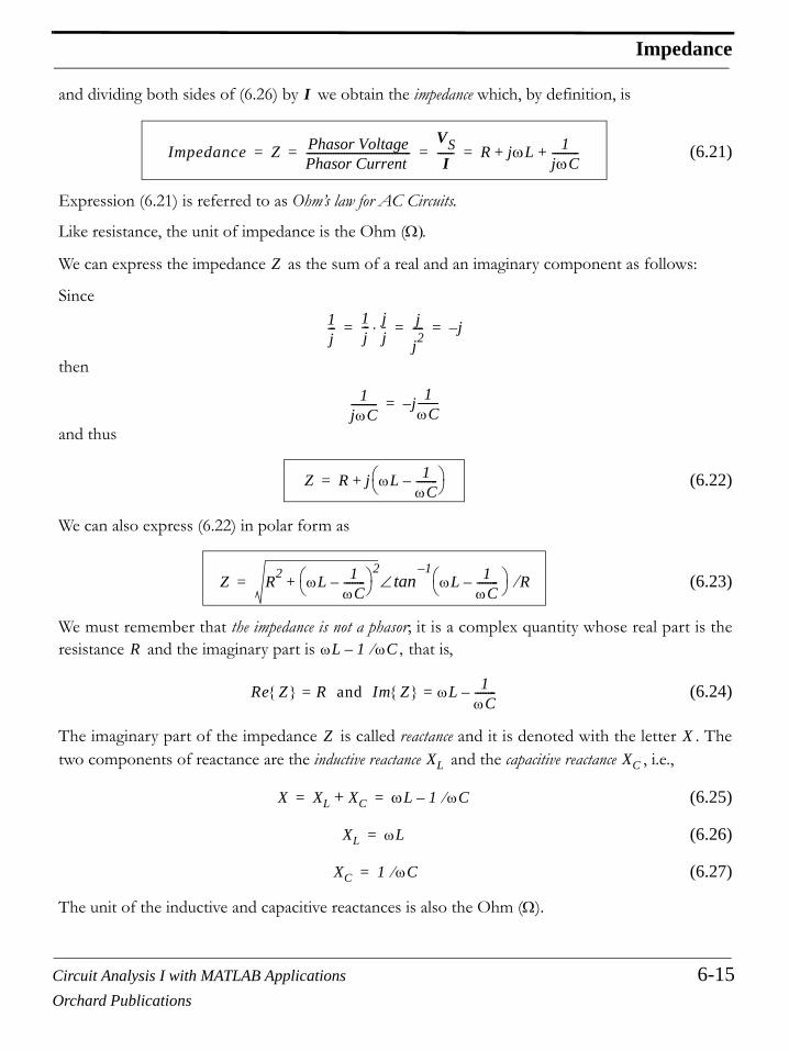
Circuit Analysis I with MATLAB Applications 6-15Orchard Publications
Impedance
and dividing both sides of (6.26) by we obtain the impedance which, by definition, is
(6.21)
Expression (6.21) is referred to as Ohm’s law for AC Circuits.
Like resistance, the unit of impedance is the Ohm (Ω).
We can express the impedance as the sum of a real and an imaginary component as follows:
Since
then
and thus
(6.22)
We can also express (6.22) in polar form as
(6.23)
We must remember that the impedance is not a phasor; it is a complex quantity whose real part is theresistance and the imaginary part is , that is,
(6.24)
The imaginary part of the impedance is called reactance and it is denoted with the letter . Thetwo components of reactance are the inductive reactance and the capacitive reactance , i.e.,
(6.25)
(6.26)
(6.27)
The unit of the inductive and capacitive reactances is also the Ohm (Ω).
I
Impedance Z Phasor VoltagePhasor Current ---------------------------------------
VSI
------ R jωL 1jωC----------+ += = = =
Z
1j--- 1
j--- j
j-⋅ j
j2---- j–= = =
1jωC---------- j 1
ωC--------–=
Z R j ωL 1ωC--------–⎝ ⎠
⎛ ⎞+=
Z R2ωL 1
ωC--------–⎝ ⎠
⎛ ⎞ 2+ ωL 1
ωC--------–⎝ ⎠
⎛ ⎞ R⁄1–
tan∠=
R ωL 1 ωC⁄–
Re Z R= and Im Z ωL 1ωC--------–=
Z XXL XC
X XL XC+ ωL 1 ωC⁄–= =
XL ωL=
XC 1 ωC⁄=

Chapter 6 Sinusoidal Circuit Analysis
6-16 Circuit Analysis I with MATLAB ApplicationsOrchard Publications
In terms of reactances, the impedance can be expressed as
(6.28)
By a procedure similar to that of Chapter 2, we can show that impedances combine as resistances do.
Example 6.9
For the circuit below, find the current given that .
Figure 6.11. Circuit for Example 6.9
Solution:
If we attempt to solve this problem in the time-domain directly, we will need to solve an integrodif-ferential equation. But as we now know, a much easier solution is with the transformation of thegiven circuit to a phasor circuit. Here, and thus
and
Also,
and the phasor circuit is as shown in Figure 6.12.
Figure 6.12. Phasor circuit for Example 6.9
From the phasor circuit of Figure 6.12
Z R jX+ R j XL XC–( )+ R2 XL XC–( )2+ XL XC–( ) R⁄[ ]1–tan∠= = =
i t( ) vS t( ) 100 100t 30°–( )cos=
+ −R L
C ++ −
−
vS t( )
i t( )
5 Ω 100 mH
100 µF
vS t( ) 100 100t 30°–( )cos=
ω 100 rad s⁄=
jωL jXL j100 0.1× j10 Ω= ==
1jωC---------- j 1
ωC--------– jXC– j 1
10 2 10 2× 10 6–×-----------------------------------------– j100–= = = =
VS 100 30°–∠=
+ −C +
+ −
−5 Ω
VS ZIS=
I −j100 Ω
j10 ΩVS
−
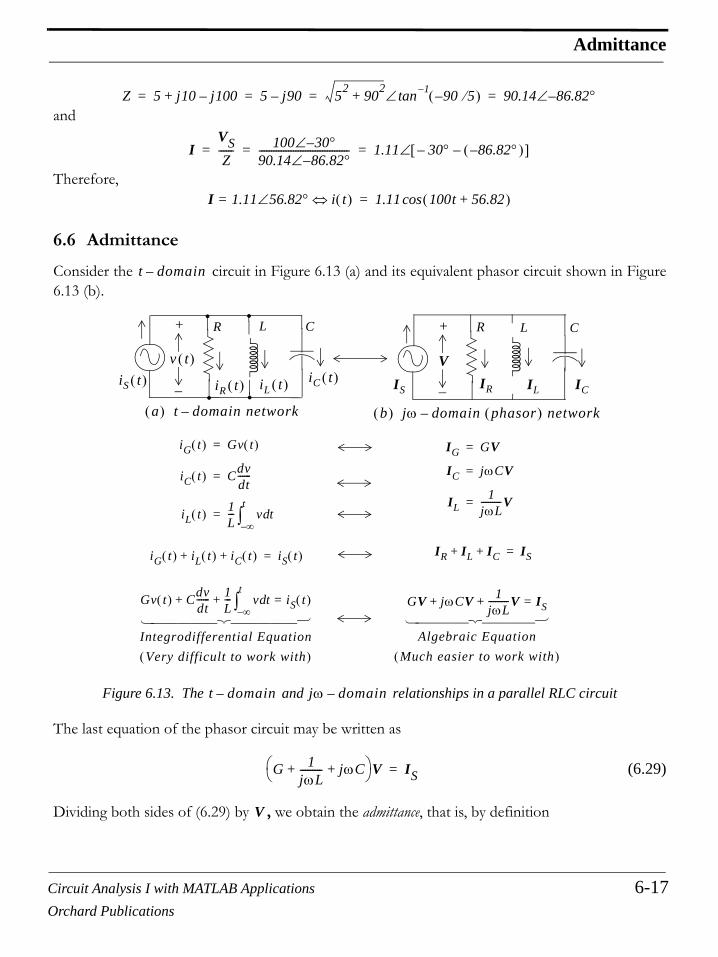
Circuit Analysis I with MATLAB Applications 6-17Orchard Publications
Admittance
and
Therefore,
6.6 Admittance
Consider the circuit in Figure 6.13 (a) and its equivalent phasor circuit shown in Figure6.13 (b).
Figure 6.13. The and relationships in a parallel RLC circuit
The last equation of the phasor circuit may be written as
(6.29)
Dividing both sides of (6.29) by , we obtain the admittance, that is, by definition
Z 5 j10 j100–+ 5 j90– 52 902+ 90– 5⁄( )1–tan∠ 90.14 86.82°–∠= = = =
IVSZ
------ 100 30°–∠90.14 86.82°–∠------------------------------------- 1.11 30°– 86.82°–( )–[ ]∠= = =
I 1.11 56.82°∠= i t( )⇔ 1.11 100t 56.82+( )cos=
t domain–
iG t( ) Gv t( )=
iC t( ) Cdvdt------=
iL t( ) 1L--- v td
∞–
t∫=
IG GV=
IC jωCV=
IL1
jωL---------V=
iG t( ) iL t( ) iC t( )+ + iS t( )= IR IL IC+ + IS=
Gv t( ) Cdvdt------ 1
L--- v td
∞–
t∫+ + iS t( )=
Integrodifferential EquationVery difficult to work with( )
⎧ ⎪ ⎪ ⎪ ⎪ ⎪ ⎨ ⎪ ⎪ ⎪ ⎪ ⎪ ⎩
GV jωCV 1jωL---------V+ + IS=
Algebraic EquationMuch easier to work with( )
⎧ ⎪ ⎪ ⎪ ⎪ ⎨ ⎪ ⎪ ⎪ ⎪ ⎩
a( ) t domain network– b( ) jω domain phasor( ) network–
+
−
V
+
−
CLR R LC
iR t( ) iL t( ) iC t( )iS t( )v t( )
IS ICIR IL
t domain– jω domain–
G 1jωL--------- jωC+ +⎝ ⎠
⎛ ⎞ V IS=
V

Chapter 6 Sinusoidal Circuit Analysis
6-18 Circuit Analysis I with MATLAB ApplicationsOrchard Publications
(6.30)
Here we observe that the admittance is the reciprocal of the impedance as conductance isthe reciprocal of the resistance .
Like conductance, the unit of admittance is the siemens or mho .
As with the impedance , we can express the admittance as the sum of a real component and animaginary component as follows:
(6.31)
and in polar form
(6.32)
Like the impedance , the admittance it is not a phasor; it is a complex quantity whose real part is the
conductance and the imaginary part is , that is,
(6.33)
The imaginary part of the admittance is called susceptance and it is denoted with the letter . Thetwo components of susceptance are the capacitive susceptance and the inductive susceptance , that is,
(6.34)
(6.35)
(6.36)
The unit of the susceptances and is also the siemens .
In terms of susceptances, the admittance can be expressed as
(6.37)
By a procedure similar to that of Chapter 2, we can show that admittances combine as conductancesdo.
Admit cetan Y Phasor CurrentPhasor Voltage ---------------------------------------
ISV----- G 1
jωL--------- jωC+ + 1
Z---= = = = =
Y Z GR
Ω 1–( )
Z Y
Y G j ωC 1ωL-------–⎝ ⎠
⎛ ⎞+=
Y G 2ωC 1
ωL-------–⎝ ⎠
⎛ ⎞ 2+ ωC 1
ωL-------–⎝ ⎠
⎛ ⎞ G⁄1–
tan∠=
Z Y
G ωC 1ωL-------–
Re Y G= and Im Y ωC 1ωL-------–=
Y BBC BL
B BC BL+ ωC 1 ωL⁄–= =
BC ωC=
BL 1 ωL⁄=
BC BL Ω 1–( )
Y
Y G jB+ G j BC BL–( )+ G 2 BC BL–( )2+ BC BL–( ) G⁄[ ]1–tan∠= = =

Circuit Analysis I with MATLAB Applications 6-19Orchard Publications
Admittance
Duality is a term meaning that there is a similarity in which some quantities are related to others.The dual quantities we have encountered thus far are listed in Table 6.1.
Example 6.10
Consider the series and parallel networks shown in Figure 6.14. How should their real and imaginaryterms be related so that they will be equivalent?
Figure 6.14. Networks for Example 6.10
Solution:
For these circuits to be equivalent, their impedances or admittances must be equal. Therefore,
and equating reals and imaginaries we get
(6.38)
Relation (6.38) is worth memorizing.
Example 6.11
Compute and for the network of Figure 6.15.
TABLE 6.1 Dual quantities
Series ParallelVoltage CurrentResistance ConductanceThevenin NortonInductance CapacitanceReactance SusceptanceImpedance Admittance
C
LRG LC
YZ
Z Y
Y 1Z--- 1
R jX+--------------- G jB+
1R jX+--------------- R jX–
R jX–---------------⋅ R jX–
R2 X2+
------------------- R
R2 X2+
------------------- j X
R2 X2+
-------------------–= = = = = =
G R
R2 X2+
-------------------= and B X–
R2 X2+
-------------------=
Z Y

Chapter 6 Sinusoidal Circuit Analysis
6-20 Circuit Analysis I with MATLAB ApplicationsOrchard Publications
Figure 6.15. Network for Example 6.11
Solution:
Since this is a parallel network, it is easier to compute the admittance first. Thus,
Since the impedance is the reciprocal of admittance, it follows that
Example 6.12
Compute and for the circuit shown below. Verify your answers with MATLAB.
Figure 6.16. Network for Example 6.12
Solution:
Let the given network be represented as shown in Figure 6.17 where ,, and
Then,
CG LZ, Y
j5 Ω 1–4 Ω 1– j2– Ω 1–
Y
Y G 1jωL--------- jωC+ + 4 j2– j5+ 4 j3+ 5 36.9°∠= = = =
Z 1Y--- 1
5 36.9°∠--------------------- 0.2 36.9– °∠ 0.16 j0.12–= = = =
Z Y
C1
Z, Y
20 Ω
−j16 Ω
j13 Ω
R2R1
L1
L2C2
10 Ω
j5 Ω
−j8 Ω
Z1 j13 j8– j5= =
Z2 10 j5+= Z3 20 j16–=
Z Z1Z2Z3
Z2 Z3+-----------------+ j5 10 j5+( ) 20 j16–( )
10 j5 20 j16–+ +-----------------------------------------------+ j5 11.18 26.6°∠( ) 25.61 38.7°–∠( )
31.95 20.1°–∠----------------------------------------------------------------------------+= = =
j5 8.96 8°∠+ j5 8.87 j1.25+ + 8.87 j6.25+ 10.85 35.2°∠= ===
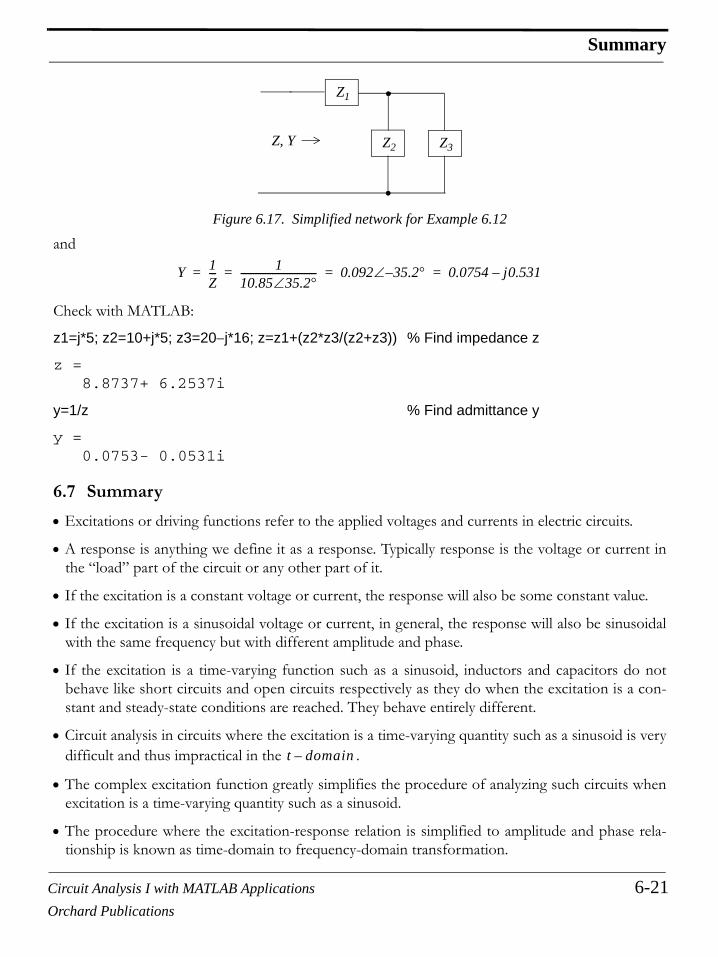
Circuit Analysis I with MATLAB Applications 6-21Orchard Publications
Summary
Figure 6.17. Simplified network for Example 6.12
and
Check with MATLAB:
z1=j*5; z2=10+j*5; z3=20−j*16; z=z1+(z2*z3/(z2+z3)) % Find impedance z
z = 8.8737+ 6.2537i
y=1/z % Find admittance y
y = 0.0753- 0.0531i
6.7 Summary
• Excitations or driving functions refer to the applied voltages and currents in electric circuits.
• A response is anything we define it as a response. Typically response is the voltage or current inthe “load” part of the circuit or any other part of it.
• If the excitation is a constant voltage or current, the response will also be some constant value.
• If the excitation is a sinusoidal voltage or current, in general, the response will also be sinusoidalwith the same frequency but with different amplitude and phase.
• If the excitation is a time-varying function such as a sinusoid, inductors and capacitors do notbehave like short circuits and open circuits respectively as they do when the excitation is a con-stant and steady-state conditions are reached. They behave entirely different.
• Circuit analysis in circuits where the excitation is a time-varying quantity such as a sinusoid is verydifficult and thus impractical in the .
• The complex excitation function greatly simplifies the procedure of analyzing such circuits whenexcitation is a time-varying quantity such as a sinusoid.
• The procedure where the excitation-response relation is simplified to amplitude and phase rela-tionship is known as time-domain to frequency-domain transformation.
Z, Y
Z1
Z2 Z3
Y 1Z--- 1
10.85 35.2°∠------------------------------- 0.092 35.2°–∠ 0.0754 j0.531–= = = =
t domain–

Chapter 6 Sinusoidal Circuit Analysis
6-22 Circuit Analysis I with MATLAB ApplicationsOrchard Publications
• The procedure where the excitation-response is put back to its sinusoidal form is known as fre-quency-domain to time-domain transformation.
• For brevity, we denote the time domain as the , and the frequency domain as the.
• If a sinusoid is given in terms of the sine function, it is convenient to convert it to a cosine functionusing the identity before converting it to the
.
• The to transformation procedure is as follows:
1. Express the given sinusoid as a cosine function
2. Express the cosine function as the real part of the complex excitation using Euler’s identity
3. Extract the magnitude and phase angle from it.
• The to transformation procedure is as follows:
1. Convert the given phasor from polar to exponential form
2. Add the radian frequency multiplied by to the exponential form
3. Extract the real part from it.
• The circuit analysis of circuits containing , , and devices, and which are excited by sinusoidalsources, is considerably simplified with the use of phasor voltages and phasor currents which werepresent by the boldface capital letters and respectively.
• Phasor quantities exist only in the
• In the the current through a resistor is always in−phase with the voltage across thatresistor
• In the the current through an inductor lags the voltage across that inductor by 90°
• In the the current through a capacitor leads the voltage across that capacitor by 90°
• In the the impedance is defined as
• Like resistance, the unit of impedance is the Ohm (Ω).
• Impedance is a complex quantity whose real part is the resistance , and the imaginary part is, that is,
t domain–
jω domain–
m t( ) A ωt θ+( )sin A ωt θ 90°–+( )cos= =jω domain–
t domain– jω domain–
jω domain– t domain–
ω t
R L C
V I
jω domain–
jω domain–
jω domain–
jω domain–
jω domain– Z
Impedance Z Phasor VoltagePhasor Current ---------------------------------------
VSI
------ R jωL 1jωC----------+ += = = =
RωL 1 ωC⁄–

Circuit Analysis I with MATLAB Applications 6-23Orchard Publications
Summary
• In polar form the impedance is expressed as
• The imaginary part of the impedance is called reactance and it is denoted with the letter . Thetwo components of reactance are the inductive reactance and the capacitive reactance , i.e.,
• The unit of the inductive and capacitive reactances is also the Ohm (Ω).
• In the the admittance is defined as
• The admittance is the reciprocal of the impedance as conductance is the reciprocal of theresistance .
• The unit of admittance is the siemens or mho .
• The admittance is a complex quantity whose real part is the conductance and the imaginary
part is , that is,
• The imaginary part of the admittance is called susceptance and it is denoted with the letter .The two components of susceptance are the capacitive susceptance and the inductive suscep-tance , that is,
• In polar form the admittance is expressed as
• The unit of the susceptances and is also the siemens .
Re Z R= and Im Z ωL 1ωC--------–=
Z R2ωL 1
ωC--------–⎝ ⎠
⎛ ⎞ 2+ ωL 1
ωC--------–⎝ ⎠
⎛ ⎞ R⁄1–
tan∠=
Z XXL XC
X XL XC– ωL 1ωC--------–= =
jω domain– Y
Admit cetan Y Phasor CurrentPhasor Voltage ---------------------------------------
ISV----- G 1
jωL--------- jωC+ + 1
Z---= = = = =
Y Z GR
Ω 1–( )
Y G
ωC 1ωL-------–
Re Y G= and Im Y ωC 1ωL-------–=
Y BBC
BL
B BC BL– ωC 1ωL-------–= =
Y G 2ωC 1
ωL-------–⎝ ⎠
⎛ ⎞ 2+ ωC 1
ωL-------–⎝ ⎠
⎛ ⎞ G⁄1–
tan∠=
BC BL Ω 1–( )

Chapter 6 Sinusoidal Circuit Analysis
6-24 Circuit Analysis I with MATLAB ApplicationsOrchard Publications
• Admittances combine as conductances do.
• In phasor circuit analysis, conductance is not necessarily the reciprocal of resistance, and suscep-tance is not the negative reciprocal of reactance. Whenever we deal with resistance and reactancewe must think of devices in series, and when we deal with conductance and susceptance we mustthink of devices in parallel. However, the admittance is always the reciprocal of the impedance
• The ratio of the phasor voltage to the phasor current exists only in the and it isnot the ratio in the . Although the ratio could yield some value, thisvalue is not impedance. Similarly, the ratio is not admittance.
• Duality is a term meaning that there is a similarity in which some quantities are related to others.
V I⁄ jω domain–
v t( ) i t( )⁄ t domain– v t( ) i t( )⁄i t( ) v t( )⁄
Circuit Analysis I with MATLAB Applications 6-25Orchard Publications
Exercises
6.8 Exercises
Multiple Choice
1. Phasor voltages and phasor currents can be used in the if a circuit contains
A. independent and dependent sources with resistors only
B. independent and dependent sources with resistors and inductors only
C. independent and dependent sources with resistors and capacitors only
D. independent and dependent sources with resistors, inductors, and capacitors
E. none of the above
2. If the excitation in a circuit is a single sinusoidal source with amplitude , radian frequency ,and phase angle , and the circuit contains resistors, inductors, and capacitors, all voltages and allcurrents in that circuit will be of the same
A. amplitude but different radian frequency and different phase angle
B. radian frequency but different amplitude and different phase angle
C. phase angle but different amplitude and different radian frequency
D. amplitude same radian frequency and same phase angle
E. none of the above
3. The sinusoid in the is expressed as
A.
B.
C.
D.
E. none of the above
4. A series RLC circuit contains two voltage sources with values and. We can transform this circuit to a phasor equivalent to find the cur-
rent by first replacing these with a single voltage source whose value is
A.
B.
t domain–
A ωθ
A ω θ
ω A θ
θ A ω
A ω θ
v t( ) 120 ωt 90°+( )sin= jω domain–
V 120e j ωt 90°+( )=
V 120e jωt=
V 120e j90°=
V 120e j0°=
v1 t( ) 100 10t 45°+( )cos=
v2 t( ) 200 5t 60– °( )sin=
v t( ) v1 t( ) v2 t( )+=
v t( ) 300 15t 15– °( )cos=
v t( ) 100 5t 105°+( )cos=

Chapter 6 Sinusoidal Circuit Analysis
6-26 Circuit Analysis I with MATLAB ApplicationsOrchard Publications
C.
D.
E. none of the above
5. The equivalent impedance of the network of Figure 6.18 is
A.
B.
C.
D.
E. none of the above
Figure 6.18. Network for Questions 5 and 6
6. The equivalent admittance of the network of Figure 6.18 isA.
B.
C.
D.
E. none of the above
7. The resistance of a coil is and the inductance of that coil is . If a currentof flows through that coil and operates at the frequency of , the pha-sor voltage across that coil is
A.
v t( ) 150 7.5t 15– °( )cos=
v t( ) 150 7.5t 15°+( )cos=
Zeq
1 j1+
1 j1–
j1–
2 j0+
−j2 Ω
j0.5 Ω
2 Ω
2 Ω
Zeq
Yeq
4 j– 1.5
1673------ j 6
73------+
1237------ j 2
37------+
2 j2–
R 1.5 Ω= L 5.3 mH=
i t( ) 4 ωt Acos= f 60Hz=
V
10 53.1° V∠
Circuit Analysis I with MATLAB Applications 6-27Orchard Publications
Exercises
B.
C.
D.
E. none of the above
8. A resistor with value is in series with a capacitor whose capacitive reactance at someparticular frequency is . A phasor current with value is flowingthrough this series combination. The voltage across this series combination is
A.
B.
C.
D.
E. none of the above
9. A conductance with value is in parallel with a capacitor whose capacitive suscep-
tance at some particular frequency is . A phasor voltage with value is applied across this parallel combination. The total current through
this parallel combination is
A.
B.
C.
D.
E. none of the above
10. If the phasor , then in the is
A.
B.
C.
D.
E. none of the above
6 0° V∠
5.3 10 3–× 90° V∠
6.8 45° V∠
R 5 Ω=
ω jXC– 5– Ω= I 8 0° A∠=
t domain–
80 ωtcos
80 ωtsin
56.6 ωt 45°–( )cos
56.6 ωt 45°+( )cos
G 0.3 Ω 1–=
ω jBC j0.3 Ω 1–=
V 10 0°∠= t domain–
3 ωt j3 ωtsin+cos
3 ωt j– 3 ωtsincos
5 ωt 53.2°+( )sin
5 ωt 53.2°+( )cos
I je j π 2⁄( )= t domain– i t( )
ωt π 2⁄+( )cos
ωt π 2⁄+( )sin
ωtcos–
ωtsin–

Chapter 6 Sinusoidal Circuit Analysis
6-28 Circuit Analysis I with MATLAB ApplicationsOrchard Publications
Problems
1. Express the sinusoidal voltage waveform of Figure 6.18 as , that is, find ,, and . Answer:
Figure 6.19. Circuit for Problem 1
2. The current through a device decays exponentially as shown by the waveform of Figure 6.20,and two values are known as indicated. Compute , that is, the current at
Answers: ,
Figure 6.20. Circuit for Problem 2
3. At what frequency is the network of Figure 6.21 operating if it is known that and ? Answer:
Figure 6.21. Circuit for Problem 3
v t( ) A ωt θ+( )cos= Aω θ v t( ) 2 1000t 36.1°+( )cos=
−2.2 ms 0.94 ms
1.62 V
0 t (ms)
v (V)
i t( )i 1( ) t 1 ms=
i t( ) 50e 750t– mA= 23.62 mA
0 1 2 3 4 5 6
i = 15.00 mA at 1.605 ms
I = 5.27 mA at 3.000 ms
I
t (ms)
i (mA)
fvS 120 ωt Vcos= i 12 ωt 36.9°–( ) Acos= f 5.533 KHz=
R L
C8 Ω
1 µF
1 mH
vSi

Circuit Analysis I with MATLAB Applications 6-29Orchard Publications
Exercises
4. In the circuit of Figure 6.22, and the symbols V and A inside the cir-
cles denote an AC voltmeter* and ammeter respectively. Assume that the ammeter has negligibleinternal resistance. The variable capacitor C is adjusted until the voltmeter reads 25 V and theammeter 5 A. Find the value of the capacitor. Answer:
Figure 6.22. Network for Problem 4
5. For the circuit shown on Figure 6.23, is it possible to adjust the variable resistor and the vari-able capacitor so that and have the same numerical value regardless of the operatingfrequency? If so, what are these values? Answer: Yes, if and
Figure 6.23. Network for Problem 5
* Voltmeters and Ammeters are discussed in Chapter 8. For this exercise, it will suffice to say that theseinstruments indicate the magnitude (absolute) values of voltage and current.
vS V 2000t θ+( ) Vcos=
C 89.6 µF=
R
L
C
2 Ω
0.5 mHV
A
Other Partof the
Network
vS
R1
C ZIN YIN
C 1 F= R1 1 Ω=
1 Ω
1 HOther Part
of theNetwork
R1 R2
ZIN
YIN
L CvS

Chapter 6 Sinusoidal Circuit Analysis
6-30 Circuit Analysis I with MATLAB ApplicationsOrchard Publications
6.9 Answers to Exercises
Multiple Choice
1.E Phasors exist in the only
2. B
3. D
4. E The voltage sources and operate at different frequencies. Therefore, to find thecurrent we must apply superposition.
5. E This value is obtained with the MATLAB code z1=2+0.5j; z2=2*(−2j)/(2−2j);z=z1+z2
z = 3.0000-0.5000i
6. C7. A ,
,
8. C
9. D
10. C
Problems
1. The crossings define half of the period T. Thus, , and one
period is . The frequency is . Then, or
Next, we find the phase angle from the figure above observing that
or
jω domain–
v1 t( ) v1 t( )
3 j0.5–
ω 2πf 2π 60× 377 r s⁄= = = jXL jωL j 377 5.3 10 3–××× j2 Ω= = =
Z 1.5 j2+ 2.5 53.13°∠= = V ZI 2.5 53.13°∠ 4 0°∠× 10 53.13°∠= = =
t axis– T 2⁄ 2.2 0.94+ 3.14 ms= =
T 6.28 ms= f 1 T⁄ 103 6.28⁄ 103 2π⁄= = = ω 2πf=
ω 2π 103 2π⁄× 1000 r s⁄==
θ π 2⁄ θ+ 2.2 ms=
−2.2 ms 0.94 ms
1.62 V
0 t (ms)
v (V)
θ

Circuit Analysis I with MATLAB Applications 6-31Orchard Publications
Answers to Exercises
Finally, we find the amplitude by observing that at , , that is,
or
Therefore,
2. The decaying exponential has the form where the time is in and thus forthis problem we need to compute the values of and using the given values. Then,
and
Division of the first equation by the second yields
or
or
or
or
and thus
θ 2.2ms π2---– 2.2 10 3– s× 2π rad
6.28 10 3– s×-------------------------------- 180°
π rad--------------×× π
2---–= =
2.2 2 180°××6.28
---------------------------------- π2---– 126.1° 90°– 36.1°= ==
A t 0= v 1.62 V=
v 0( ) 1.62 A 0 36.1°+( )cos= =
A 1.6236.1°cos
---------------------- 2 V= =
v t( ) 2 1000t 36.1°+( )cos=
i t( ) Ae αt– mA= msA α
i t 1.605 ms=15 mA Ae 1.605 10 3–×( )α–= =
i t 3.000 ms=5.27 mA Ae 3.000 10 3–×( )α–= =
Ae 1.605 10 3–×( )α–
Ae 3.000 10 3–×( )α–-------------------------------------- 15 mA
5.27 mA---------------------=
e 1.605 10 3–×( )α– 3.000 10 3–×( )α+ 155.27----------=
e1.395 10 3– α× 155.27----------=
155.27----------⎝ ⎠
⎛ ⎞ln 1.395 10 3– α×=
α 15 5.27⁄( )ln 103×1.395
--------------------------------------------- 750= =
i t( ) Ae 750t– mA=
Chapter 6 Sinusoidal Circuit Analysis
6-32 Circuit Analysis I with MATLAB ApplicationsOrchard Publications
To find the value of we make use of the fact that . Then,
or
or
Therefore,
and
3. The equivalent phasor circuit is shown below.
In the , , , and Then,
and
or
or
or
or
or
A i t 3 ms=5.27 mA=
5.27 Ae 750 3 10 3–××–=
A 5.27 10 3–×
e 2.25–---------------------------=
A 0.050 A 50mA= =
i t( ) 50e 750t– mA=
i t 1 ms=50e 750 10 3–×– 23.62 mA= =
R L
C8 Ω
1 µFvS
I
jωLj
ωC--------–
jω domain– VS 120 0° V∠= I 12 36.9° A–∠= jωL j10 3– ω= j ωC⁄– j106– ω⁄=
ZVSI
------ 120 0° V∠12 36.9° A–∠--------------------------------- 10 36.9°∠= = =
Z 10 R 2 ωL 1 ωC⁄–( )2+= =
R 2 ωL 1 ωC⁄–( )2+ 100=
8 2 ωL 1 ωC⁄–( )2+ 100=
ωL 1 ωC⁄–( )2 36=
ωL 1 ωC⁄– 6=

Circuit Analysis I with MATLAB Applications 6-33Orchard Publications
Answers to Exercises
or
Solving for and ignoring the negative value, we get
and
Check: ,
and
4. Since the instruments read absolute values, we are only need to be concerned the magnitudes ofthe phasor voltage, phasor current, and impedance. Thus,
or
and after simplification we get
Using MATLAB, we get
p=[500 250*10^(−4) −625*10^(−8)]; r=roots(p)
and this yields
The second root of this polynomial is negative and thus it is discarded.
5. We group the series devices as shown below.
ω2 6L---ω– 1
LC-------– 0=
ω2 6 10 3× ω– 10 9– 0=
ω
ω 6 103× 36 106× 4 109×++2
------------------------------------------------------------------------- 34 765 r s⁄,= =
f ω2π------ 34 765 r s⁄,
2π---------------------------- 5 533 Hz, 5.533 KHz= = = =
jωL j34.765= j– ωC⁄ j28.765–=
Z R j ωL 1 ωC( )⁄–( )+ 8 j 34.765 28.765–( )+ 8 j6+ 10 36.9°∠= = = =
I 120 0°∠10 36.9°∠------------------------ 12 36.9°–∠= =
V Z I 25 R 2 ωL 1 ωC⁄–( )2+ 5×= = =
V 2 252 R 2 ωL 1 ωC⁄–( )2+[ ] 25× 4 1 5 10 4–×C
--------------------–⎝ ⎠⎛ ⎞
2+ 25×= = =
100 25 250 10 4–×C
--------------------------– 625 10 8–×
C 2--------------------------+ + 625==
500C 2 250 10 4– C× 625 10 8–×–+ 0=
C 89.6 µF=

Chapter 6 Sinusoidal Circuit Analysis
6-34 Circuit Analysis I with MATLAB ApplicationsOrchard Publications
Thus , , and
and at any frequency
Therefore, if the condition is to hold for all frequencies, the right sides of and must be equal, that is,
Equating reals and imaginaries we get
From the first equation above we get and by substitution of this value into the secondequation we get
1 Ω
1 H
R1 R2
ZIN
YIN
L C
Z1 Z2
Z1 R1 jω+= Z2 1 j ωC( )⁄–=
ZINZ1 Z2⋅Z1 Z2+-----------------
R1 jω+( ) 1 j ωC⁄–( )R1 jω 1 j ωC⁄–+ +
---------------------------------------------------= =
ω
YIN1
ZIN--------
R1 jω 1 j ωC⁄–+ +
R1 jω+( ) 1 j ωC⁄–( )---------------------------------------------------= =
YIN ZIN= ZIN
YIN
R1 jω+( ) 1 j ωC⁄–( )R1 jω 1 j ωC⁄–+ +
---------------------------------------------------R1 jω 1 j ωC⁄–+ +
R1 jω+( ) 1 j ωC⁄–( )---------------------------------------------------=
R1 jω+( ) 1 j ωC⁄–( )[ ] 2 R1 jω 1 j ωC⁄–+ +[ ] 2=
R1 jω+( ) 1 j ωC⁄–( ) R1 jω 1 j ωC⁄–+ +=
R1 jR1ωC--------– jω 1
C----+ + R1 1 j ω 1
ωC--------–⎝ ⎠
⎛ ⎞+ +=
R11C----+⎝ ⎠
⎛ ⎞ j ωR1ωC--------–⎝ ⎠
⎛ ⎞ jω+ + R1 1+( ) j ω 1ωC--------–⎝ ⎠
⎛ ⎞+=
R11C----+ R1 1+= ω
R1ωC--------– ω 1
ωC--------–=
C 1 F=
R1 1 Ω=

Circuit Analysis I with MATLAB Applications 7-1Orchard Publications
Chapter 7
Phasor Circuit Analysis
his chapter begins with the application of nodal analysis, mesh analysis, superposition, andThevenin’s and Norton’s theorems in phasor circuits. Then, phasor diagrams are introduced,and the input-output relationships for an RC low-pass filter and an RC high-pass filter are
developed.
7.1 Nodal Analysis
The procedure of analyzing a phasor* circuit is the same as in Chapter 3, except that in this chapterwe will be using phasor quantities. The following example illustrates the procedure.
Example 7.1
Use nodal analysis to compute the phasor voltage for the circuit of Figure 7.1.
Figure 7.1. Circuit for Example 7.1
Solution:
As before, we choose a reference node as shown in Figure 7.2, and we write nodal equations at theother two nodes and . Also, for convenience, we designate the devices in series as
as shown, and then we write the nodal equations in terms of these impedances.
* A phasor is a rotating vector
T
VAB VA VB–=
10 0° A∠5 0° A∠
VBVA
4 Ω
j– 6 Ω
2 Ω8 Ω
j3 Ω
j– 3 Ω
A BZ1 Z2 and Z3, ,
Z1 4 j6– 7.211 56.3°–∠= =
Z2 2 j3+ 3.606 56.3°∠= =
Z3 8 j3– 8.544 20.6°–∠= =

Chapter 7 Phasor Circuit Analysis
7-2 Circuit Analysis I with MATLAB ApplicationsOrchard Publications
Figure 7.2. Nodal analysis for the circuit for Example 7.1
By application of KCL at ,
or
(7.1)
or
and by substitution for we get
(7.2)
Next, at :
or
10 0° A∠5 0° A∠
VBVA
4 Ω
j– 6 Ω
2 Ω8 Ω
j3 Ω
j– 3 ΩZ1 Z3
Z2
VA
VAZ1------
VA VB–
Z2-------------------+ 5 0°∠=
1Z1----- 1
Z2-----+⎝ ⎠
⎛ ⎞ VA1Z2-----VB– 5 0°∠=
Z1 Z2+
Z1Z2-----------------⎝ ⎠
⎛ ⎞ VA1
Z2------VB– 5 0°∠=
Z1 and Z2
4 j6– 2 j3+ +7.211 56.3–∠( ) 3.606 56.3°∠( )
--------------------------------------------------------------------------VA1
3.606 56.3°∠-------------------------------VB– 5 0°∠=
6 j3–26.0 0°∠---------------------VA 0.277 56.3°–∠( )VB– 5 0°∠=
6.708 26.6°–∠26 0°∠
----------------------------------VA 0.277 56.3°–∠( )VB– 5 0°∠=
0.258 26.6°–∠( )VA 0.277 56.3°–∠( )VB– 5 0°∠=
VB
VB VA–
Z2-------------------
VBZ3------+ 10– 0°∠=

Circuit Analysis I with MATLAB Applications 7-3Orchard Publications
Nodal Analysis
(7.3)
In matrix form (7.1) and (7.3) are
(7.4)
We will follow a step-by-step procedure to solve these equations using Cramer’s rule, and we willuse MATLAB®* to verify the results.
We rewrite (7.3) as
(7.5)
and thus with (7.2) and (7.5) the system of equations is
(7.6)
We find and from
(7.7)
and
(7.8)
The determinant is
* If unfamiliar with MATLAB, please refer to Appendix A
1Z2-----VA– 1
Z2----- 1
Z3-----+⎝ ⎠
⎛ ⎞ VB+ 10– 0°∠=
1Z1----- 1
Z2-----+⎝ ⎠
⎛ ⎞ 1Z2-----–
1Z2-----– 1
Z2----- 1
Z3-----+⎝ ⎠
⎛ ⎞
VA
VB
510–
=
1Z2-----VA–
Z2 Z3+
Z2Z3-----------------⎝ ⎠
⎛ ⎞ VB+ 10 180°∠=
13.606 56.3°∠-------------------------------VA–
2 j3 8 j3–+ +3.606 56.3°∠( ) 8.544 20.6°–∠( )
----------------------------------------------------------------------------VB+ 10 180°∠=
0.277 56.3°–∠( )VA–10
30.810 35.7°∠----------------------------------VB+ 10 180°∠=
0.277 56.3°–∠( )VA– 0.325 35.7°–∠( )VB+ 10 180°∠=
0.258 26.6°–∠( )VA 0.277 56.3°–∠( )VB– 5 0°∠=
0.277 56.3°–∠( )VA– 0.325 35.7°–∠( )VB+ 10 180°∠=
VA VB
VAD1
∆------=
VBD2
∆------=
∆

Chapter 7 Phasor Circuit Analysis
7-4 Circuit Analysis I with MATLAB ApplicationsOrchard Publications
Also,
and
Therefore, by substitution into (7.7) and (7.8), we get
and
Finally,
Check with MATLAB:
z1=4−j*6; z2=2+j*3; z3=8−j*3; % Define z1, z2 and z3Z=[1/z1+1/z2 −1/z2; −1/z2 1/z2+1/z3]; % Elements of matrix ZI=[5 −10]'; % Column vector IV=Z\I; Va=V(1,1); Vb=V(2,1); Vab=Va−Vb; % Va = V(1), Vb = V(2) are also acceptable% With fprintf only the real part of each parameter is processed so we will use dispfprintf(' \n'); disp('Va = '); disp(Va); disp('Vb = '); disp(Vb); disp('Vab = '); disp(Vab);fprintf(' \n');
∆ 0.258 26.6°–∠( ) 0.277 56.3°–∠( )–
0.277 56.3°–∠( )– 0.325 35.7°–∠( )=
0.258 26.6°–∠( ) 0.325 35.7°–∠( )⋅ 0.277 56.3°–∠( ) 0.277– 56.3–∠( )⋅–=
0.084 62.3°–∠( ) 0.077 112.6–∠( )– 0.039 j0.074–( ) 0.023– j0.071–( )––=
0.062 j0.003– 0.062 2.8°–∠=( )=
D15 0°∠ 0.277 56.3°–∠( )–
10 180°∠ 0.325 35.7°–∠( )=
5 0°∠( ) 0.325 35.7°–∠( ) 10 180°∠( ) 0.277 56.3°–∠( )–[ ]–=
1.625 35.7°–∠ 2.770 123.7°∠+( ) 1.320 j0.948– 1.537– j2.305+( )+==
0.217– j1.357+ 1.374 99.1°∠==
D20.258 26.6°–∠( ) 5 0°∠0.277 56.3°–∠( )– 10 180°∠
=
0.258 26.6°–∠( ) 10 180°∠( ) 0.277– 56.3°–∠( ) 5 0°∠( )–=
2.580 153.4°∠ 1.385 56.3°–∠+ 2.307– j1.155 0.769 j1.152–+ +( )==
1.358– j0.003+ 1.358 179.9°∠==
VAD1
∆------ 1.374 99.1°∠
0.062 2.8°–∠------------------------------- 22.161 101.9°∠ 4.570– j21.685+= = = =
VBD2
∆------ 1.358 179.9°∠
0.062 2.8°–∠---------------------------------- 24.807 177.3°–∠ 24.780– j1.169–= = = =
VAB VA VB– 4.570– j21.685 24.780– j1.169–( )–+= =
20.21 j22.85+ 30.5 48.5°∠==

Circuit Analysis I with MATLAB Applications 7-5Orchard Publications
Mesh Analysis
Va = -4.1379 + 19.6552i
Vb = -22.4138 - 1.0345i
Vab = 18.2759 + 20.6897i
These values differ by about 10% from the values we obtained with Cramer’s rule where werounded the values to three decimal places. MATLAB performs calculations with accuracy of 15decimal places, although it only displays four decimal places in the short (default) number displayformat. Accordingly, we should accept the MATLAB values as more accurate.
7.2 Mesh Analysis
Again, the procedure of analyzing a phasor circuit is the same as in Chapter 3 except that in thischapter we will be using phasor quantities. The following example illustrates the procedure.
Example 7.2
For the circuit of Figure 7.3, use mesh analysis to find the voltage , that is, the voltage acrossthe current source.
Figure 7.3. Circuit for Example 7.2
Solution:
As in the previous example, for convenience, we denote the passive devices in series as, and we write mesh equations in terms of these impedances. The circuit then is as
shown in Figure 7.4 with the mesh currents assigned in a clockwise direction.
We observe that the voltage across the current source is the same as the voltage across the and series combination.
By inspection, for Mesh 1,
(7.9)
V10A
10 0°∠
10 0° A∠5 0° A∠
4 Ω
j– 6 Ω
2 Ω
8 Ω
j3 Ω
j– 3 Ω
V10A
+
−
Z1 Z2 and Z3, ,
10 0°∠8 Ω j– 3 Ω
I1 5 0°∠=
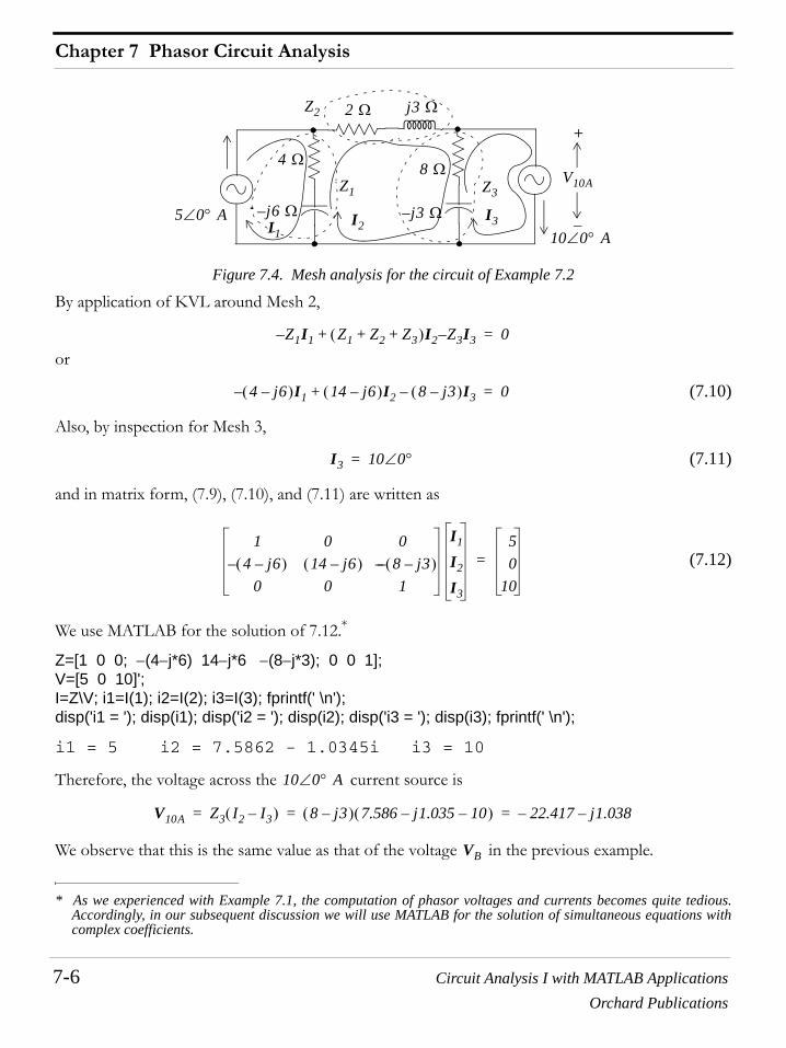
Chapter 7 Phasor Circuit Analysis
7-6 Circuit Analysis I with MATLAB ApplicationsOrchard Publications
Figure 7.4. Mesh analysis for the circuit of Example 7.2
By application of KVL around Mesh 2,
or
(7.10)
Also, by inspection for Mesh 3,
(7.11)
and in matrix form, (7.9), (7.10), and (7.11) are written as
(7.12)
We use MATLAB for the solution of 7.12.*
Z=[1 0 0; −(4−j*6) 14−j*6 −(8−j*3); 0 0 1];V=[5 0 10]';I=Z\V; i1=I(1); i2=I(2); i3=I(3); fprintf(' \n');disp('i1 = '); disp(i1); disp('i2 = '); disp(i2); disp('i3 = '); disp(i3); fprintf(' \n');
i1 = 5 i2 = 7.5862 - 1.0345i i3 = 10
Therefore, the voltage across the current source is
We observe that this is the same value as that of the voltage in the previous example.
* As we experienced with Example 7.1, the computation of phasor voltages and currents becomes quite tedious.Accordingly, in our subsequent discussion we will use MATLAB for the solution of simultaneous equations withcomplex coefficients.
10 0° A∠5 0° A∠
4 Ω
j– 6 Ω
2 Ω
8 Ω
j3 Ω
j– 3 Ω
V10A
+
−
Z2
Z1 Z3
I2I1I3
Z1I1 Z1 Z2 Z3+ +( )I2 Z3I3–+– 0=
4 j6–( )– I1 14 j6–( )I2 8 j3–( )I3–+ 0=
I3 10 0°∠=
1 0 04 j6–( )– 14 j6–( ) 8 j3–( )––
0 0 1
I1
I2
I3
50
10
=
10 0° A∠
V10A Z3 I2 I3–( ) 8 j3–( ) 7.586 j1.035– 10–( ) 22.417– j1.038–= = =
VB

Circuit Analysis I with MATLAB Applications 7-7Orchard Publications
Application of Superposition Principle
7.3 Application of Superposition Principle
As we know from Chapter 3, the superposition principle is most useful when a circuit contains twoor more independent voltage or current sources. The following example illustrates the applicationof the superposition principle in phasor circuits.
Example 7.3
Use the superposition principle to find the phasor voltage across capacitor in the circuit of Fig-ure 7.5.
Figure 7.5. Circuit for Example 7.3
Solution:
Let the phasor voltage across due to the current source acting alone be denoted as, and that due to the current source as . Then,
With the current source acting alone, the circuit reduces to that shown in Figure 7.6.
Figure 7.6. Circuit for Example 7.3 with the current source acting alone
By application of the current division expression, the current through is
The voltage across with the current source acting alone is
C2
10 0° A∠5 0° A∠
4 Ω
j– 6 Ω
2 Ω8 Ω
j3 Ω
j– 3 ΩC2
C2 5 0° A∠
V 'C2 10 0° A∠ V ''C2
VC2 V 'C2 V ''C2+=
5 0° A∠
5 0° A∠
4 Ω
j– 6 Ω
2 Ω8 Ω
j3 Ω
j– 3 ΩC2
V 'C2
5 0° A∠
I 'C2 C2
I 'C24 j6–
4 j6– 2 j3 8 j3–+ + +-------------------------------------------------------5 0°∠ 7.211 56.3°–∠
15.232 23.2°–∠-------------------------------------5 0°∠ 2.367 33.1°–∠= = =
C2 5 0°∠

Chapter 7 Phasor Circuit Analysis
7-8 Circuit Analysis I with MATLAB ApplicationsOrchard Publications
(7.13)
Next, with the current source acting alone, the circuit reduces to that shown in Figure 7.7.
Figure 7.7. Circuit for Example 7.3 with the current source acting alone
and by application of the current division expression, the current through is
The voltage across with the current source acting alone is
(7.14)
Addition of (7.13) with (7.14) yields
or
(7.15)
7.4 Thevenin’s and Norton’s Theorems
These two theorems also offer a very convenient method in analyzing phasor circuits as illustrated bythe following example.
Example 7.4
For the circuit of Figure 7.8, apply Thevenin’s theorem to compute and then draw Norton’sequivalent circuit.
V 'C2 j3–( ) 2.367 33.1°–∠( ) 3 90°–∠( ) 2.367 33.1°–∠( )= =
7.102 123.1°–∠ 3.878– j5.949–==
10 0° A∠
10 0° A∠
4 Ω
j– 6 Ω
2 Ω8 Ω
j3 Ω
j– 3 ΩC2
V ''C2
10 0° A∠
I ''C2 C2
I ''C24 j6– 2 j3+ +
4 j6– 2 j3 8 j3–+ + +------------------------------------------------------- 10– 0°∠( )=
6.708 26.6°–∠15.232 23.2°–∠-------------------------------------10 180°∠ 4.404 176.6°∠==
C2 10 0°∠
V ''C2 j3–( ) 4.404 176.6°∠( ) 3 90°–∠( ) 4.404 176.6°∠( )= =
13.213 86.6∠ 0.784 j13.189+=( )=
VC2 V 'C2 V ''C2+ 3.878– j5.949– 0.784 j13.189+ += =
VC2 3.094– j7.240+ 7.873 113.1°∠= =
IX

Circuit Analysis I with MATLAB Applications 7-9Orchard Publications
Thevenin’s and Norton’s Theorems
Figure 7.8. Circuit for Example 7.4
Solution:
With the resistor disconnected, the circuit reduces to that shown in Figure 7.9.
Figure 7.9. Circuit for Example 7.4 with the resistor disconnected
By application of the voltage division expression,
(7.16)
and
(7.17)
Then, from (7.16) and (7.17),
or
(7.18)
Next, we find the Thevenin equivalent impedance by shorting the voltage source.The circuit then reduces to that shown in Figure 7.10.
170 0° V∠
j100– Ω85 Ω
50 Ω100 Ω
j200 Ω
IX
100 Ω
170 0° V∠
j100– Ω85 Ω
50 Ωj200 Ω
V1 V2
100 Ω
V1j200
85 j200+-----------------------170 0°∠ 200 90°∠
217.31 67°∠------------------------------170 0°∠ 156.46 23°∠ 144 j61.13+= = = =
V250
50 j100–-----------------------170 0°∠ 50
111.8 63.4–( )°∠---------------------------------------170 0°∠ 76 63.4°∠ 34 j68+= = = =
VTH VOC V12 V1 V2– 144 j61.13 34 j68+( )–+= = = =
VTH 110 j6.87– 110.21 3.6– °∠= =
ZTH 170 0° V∠

Chapter 7 Phasor Circuit Analysis
7-10 Circuit Analysis I with MATLAB ApplicationsOrchard Publications
Figure 7.10. Circuit for Example 7.4 with the voltage source shorted
We observe that the parallel combinations and are in series as shown in Figure7.11.
Figure 7.11. Network for the computation of for Example 7.4
From Figure 7.11,
and with MATLAB,
Zth=85*200j/(85+200j) + 50*(−100j)/(50−100j)
Zth = 1.1200e+002 + 1.0598e+001i
or
The Thevenin equivalent circuit is shown in Figure 7.12.
j100– Ω85 Ω
50 Ωj200 Ω
X Y
j100– Ω85 Ω
50 Ωj200 Ω
X Y
j100– Ω85 Ω
50 Ωj200 Ω
X Y
j100– Ω85 Ω
50 Ωj200 Ω
X Y
j100– Ω85 Ω
50 Ωj200 Ω
X Y ZTH
85 Ω
50 Ω
j200 Ω
X
Yj100– Ω
j200 || 85 50 || j100
85 Ωj200 Ω
−j100 Ω50 Ω
Y
X
ZTH
ZTH
ZTH85 j200×85 j200+----------------------- 50 j100–( )×
50 j100–-------------------------------+=
ZTH 112.0 j10.6+ 112.5 5.4° Ω∠= =

Circuit Analysis I with MATLAB Applications 7-11Orchard Publications
Thevenin’s and Norton’s Theorems
Figure 7.12. Thevenin equivalent circuit for Example 7.4
With the resistor connected at X-Y, the circuit becomes as shown in Figure 7.13.
Figure 7.13. Simplified circuit for computation of in Example 7.4
We find using MATLAB:
Vth=110−6.87j; Zth=112+10.6j; Ix=Vth/(Zth+100);fprintf(' \n'); disp('Ix = '); disp(Ix); fprintf(' \n');
Ix = 0.5160 - 0.0582i
that is,
(7.19)
The same answer is found in Example C.18 of Appendix where we applied nodal analysis to find.
Norton’s equivalent is obtained from Thevenin’s circuit by exchanging and its series with in parallel with as shown in Figure 7.14. Thus,
and
VTH = 110.21∠−3.6°
112 Ω j10.6 ΩX
Y
ZTH
= 110−j6.87
100 Ω
VTH = 110−j6.87 100 Ω
j10.6 Ω
X
Y
112 ΩIX
IX
IX
IXVTH
ZTH 100 Ω+--------------------------------- 0.516 j0.058– 0.519 6.4° A–∠= = =
CIX
VTH ZTH
IN ZN
INVTHZTH---------- 110.21 3.6°–∠
112.5 5.4°∠---------------------------------- 0.98 9° A–∠= = =
ZN ZTH 112.5 5.4° Ω∠= =

Chapter 7 Phasor Circuit Analysis
7-12 Circuit Analysis I with MATLAB ApplicationsOrchard Publications
Figure 7.14. Norton equivalent circuit for Example 7.4
7.5 Phasor Analysis in Amplifier Circuits
Other circuits such as those who contain op amps and op amp equivalent circuits can be analyzedusing any of the above methods.
Example 7.5
Compute for the circuit below where .
Figure 7.15. Circuit for Example 7.5
Solution:
As a first step, we perform the , to transformation. Thus,
and
Also,
and the phasor circuit is shown in Figure 5.16.
IN
ZN
iX t( ) vin t( ) 2 30000ωt( ) Vcos=
+
−
+
−0.2 mH
8 Ω
2 Ω
10 Ω
50 Ω
4 Ω
iX t( )
vC t( )vin t( )
5vC t( )10 3⁄ µF
t domain– jω domain–
jXL jωL j0.2 10 3– 30 103××× j6= = =
jXC– j–1
ωC-------- j–
1
30 103× 103
------ 10 6–××-------------------------------------------------- j10–= = =
VIN 2 0°∠=

Circuit Analysis I with MATLAB Applications 7-13Orchard Publications
Phasor Analysis in Amplifier Circuits
Figure 7.16. Phasor circuit for Example 7.5
At Node :
(7.20)
and since
the nodal equation of (7.20) simplifies to
(7.21)
At Node :
or
(7.22)
At Node :
We use MATLAB to solve (7.21) and (7.22).
G=[35/50 −j*3/50; −1/5 1/10+j*1/10]; I=[1 0]'; V=G\I;Ix=5*V(2,1)/4; % Multiply Vc by 5 and divide by 4 to get current IxmagIx=abs(Ix); theta=angle(Ix)*180/pi; % Convert current Ix to polar formfprintf(' \n'); disp(' Ix = ' ); disp(Ix);...fprintf('magIx = %4.2f A \t', magIx); fprintf('theta = %4.2f deg \t', theta);...fprintf(' \n'); fprintf(' \n');
Ix = 2.1176 - 1.7546i magIx = 2.75 A theta = -39.64 deg
+
−
+
−−j10 Ω
8 Ω2 Ω 10 Ω
50 Ω
4 Ω
2 0°∠
+
−
IX
VIN
V1
5VC
VC
V2 V3
j6 Ω
V1 2 0°∠–
2--------------------------
V18 j6+--------------
V1 VC–
10-------------------
V1 5VC–
50----------------------+ + + 0=
18 j6+-------------- 1
8 j6+-------------- 8 j– 6
8 j– 6-----------⋅ 8 j– 6
100----------- 4
50------ j 3
50------–= = =
3550------ j 3
50------–⎝ ⎠
⎛ ⎞ V115---VC– 1 0°∠=
VC V1–
10-------------------
VCj10–
-----------+ 0=
110------V1– 1
10------ j 1
10------+⎝ ⎠
⎛ ⎞ VC+ 0=
V3 5VC=

Chapter 7 Phasor Circuit Analysis
7-14 Circuit Analysis I with MATLAB ApplicationsOrchard Publications
Therefore,
Example 7.6
Compute the phasor for the op amp circuit of Figure 7.17.
Figure 7.17. Circuit for Example 7.6
Solution:
We assign phasor voltages and as shown in Figure 7.18, and we apply KCL at these nodes,
while observing that
Figure 7.18. Application of KCL for the circuit of Example 7.6
At Node :
or
(7.23)
At Node ,
I 2.75 39.6°–∠= i t( ) 2.75 30000t 39.6°–( )cos=⇔
Vout
4 Ω
−j5 Ω
−j10 Ω
5 Ω
10 ΩVout
Vin 4 0° V∠=
V1 V +
Vout V +=
4 Ω
−j10 Ω
5 Ω
10 Ω
V1
V +
Vin 4 0° V∠= Vout
V1 4 0°∠–
4--------------------------
V1 Vout–
j5–-----------------------
V1 Vout–
5-----------------------
V1j10–
-----------+ + + 0=
920------ j 3
10------+⎝ ⎠
⎛ ⎞ V115--- j15
---+⎝ ⎠⎛ ⎞ Vout– 1 0°∠=
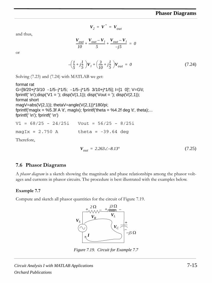
Circuit Analysis I with MATLAB Applications 7-15Orchard Publications
Phasor Diagrams
and thus,
or
(7.24)
Solving (7.23) and (7.24) with MATLAB we get:
format ratG=[9/20+j*3/10 −1/5−j*1/5; −1/5−j*1/5 3/10+j*1/5]; I=[1 0]'; V=G\I;fprintf(' \n');disp(‘V1 = ’); disp(V(1,1)); disp(‘Vout = ’); disp(V(2,1));format shortmagV=abs(V(2,1)); thetaV=angle(V(2,1))*180/pi; fprintf('magIx = %5.3f A \t', magIx); fprintf('theta = %4.2f deg \t', theta);...fprintf(' \n'); fprintf(' \n')
V1 = 68/25 - 24/25i Vout = 56/25 - 8/25i
magIx = 2.750 A theta = -39.64 deg
Therefore,
(7.25)
7.6 Phasor Diagrams
A phasor diagram is a sketch showing the magnitude and phase relationships among the phasor volt-ages and currents in phasor circuits. The procedure is best illustrated with the examples below.
Example 7.7
Compute and sketch all phasor quantities for the circuit of Figure 7.19.
Figure 7.19. Circuit for Example 7.7
V2 V + Vout= =
Vout10
-----------Vout V1–
5-----------------------
Vout V1–
j5–-----------------------+ + 0=
15--- j15
---+⎝ ⎠⎛ ⎞– V1
310------ j15
---+⎝ ⎠⎛ ⎞ Vout+ 0=
Vout 2.263 8.13°–∠=
VS
VC +
−
j3 Ω
−j5 Ω
2 Ω
I
VL VR
++ −−

Chapter 7 Phasor Circuit Analysis
7-16 Circuit Analysis I with MATLAB ApplicationsOrchard Publications
Solution:
Since this is a series circuit, the phasor current I is common to all circuit devices. Therefore, weassign to this phasor current the value and use it as our reference as shown in the phasordiagram of Figure 7.20. Then,
Figure 7.20. Phasor diagram for the circuit of Example 7.7
Example 7.8
Compute and sketch all phasor quantities for the circuit of Figure 7.21.
Figure 7.21. Circuit for Example 7.8
Solution:
Since this is a parallel circuit, the phasor voltage V is common to all circuit devices. Therefore let usassign this phasor voltage the value and use it as our reference phasor as shown in thephasor diagram of Figure 7.22. Then,
I 1 0°∠=
VR 2 Ω( ) 1 0°∠( ) 2 0° V∠= =
VL j3 Ω( ) 1 0°∠( ) j3 3 90° V∠= = =
VC j– 5 Ω( ) 1 0°∠( ) j5– 5 90– ° V∠= = =
VS VR VL VC+( )+ 2 j2– 2 2 45°–∠= = =
I = 1∠0°VR
VL
VC
VL+VCVS=VR+(VL+VC)
IS
IC
j20 Ω −j10 Ω10 ΩV
IL IR +
−
V 1 0°∠=

Circuit Analysis I with MATLAB Applications 7-17Orchard Publications
Phasor Diagrams
Figure 7.22. Phasor diagram for Example 7.8
We can draw a phasor diagram for other circuits that are neither series nor parallel by assigning anyphasor quantity as a reference.
Example 7.9
Compute and sketch all phasor voltages for the circuit of Figure 7.23. Then, use MATLAB to plotthese quantities in the .
Figure 7.23. Circuit for Example 7.9
Solution:
We will begin by selecting as our reference as shown on the phasor diagram of Fig-ure 7.24. Then,
IR 1 0°∠ 10⁄ 100 0° mA∠= =
IL 1 0°∠ j20⁄ 1 0°∠ 20 90°∠⁄ 50 90– ° m∠= = =
IC 1 0°∠ j– 10( )⁄ 1 0°∠ 10 90– °∠⁄ 100 90° mA∠= = =
IC IL+ 50 90° mA∠=
IS IR IC IL+( )+ 100 j50+ 111.8 26.6°∠= = =
V = 1∠0°
IR
IC
IL
IC+ILIS=IR+(IC+IL)
t domain–
VS VC
+
−
j3 Ω
−j5 Ω
2 Ω
VL VR1 ++ −−
5 Ω+
−
VR2
IR2
IR2 1 0° A∠=
VR2 5 Ω IR2× 5 1 0°∠×= 5 0°∠= =
VL j3 Ω IR2× 3 90°∠ 1 0°∠×= 3 90°∠= =
VC VL VR2+ 5 0°∠ 3 90°∠+ 5 j3+= 5.83 31°∠= = =

Chapter 7 Phasor Circuit Analysis
7-18 Circuit Analysis I with MATLAB ApplicationsOrchard Publications
and
Figure 7.24. Phasor diagram for Example 7.9
Now, we can transform these phasors into time-domain quantities and use MATLAB to plot them.We will use the voltage source as a reference with the value , and we will apply nodalanalysis with node voltages V1, V2, and V3 assigned as shown in Figure 7.25.
Figure 7.25. Circuit for Example 7.9 with the voltage source taken as reference
The node equations are shown below in matrix form.
The MATLAB code is as follows:
VR1 2 Ω IR1× 2 IC IR2+( ) 2VCj5–
-------- IR2+⎝ ⎠⎛ ⎞ 2 5.83 31°∠
5 90°–∠------------------------ 5 0° ∠+⎝ ⎠
⎛ ⎞== = =
2.33 121° 10 0° ∠+∠ 1.2– j2+ 10+ 8.8 j2+ 9 12.8°∠= = ==
VS VR1 VC+ 8.8 j2 5 j3+ + + 13.8 j5+ 14.7 20°∠= = = =
IR2 1 0° A∠=VR2 5 0°∠=
VL 3 90°∠=
VC 5.83 31°∠=
VR1 9 12.8°∠=
VS 14.7 20°∠=
VS 1 0°∠=
VS VC
+
−
j3 Ω
−j5 Ω
2 Ω
VL VR1 ++ −−
5 Ω+
−VR2
IR2
V3 V1 V2
1 0° V∠
1 0 012---– 1
2--- 1
j5–-------- 1
j3-----+ +⎝ ⎠
⎛ ⎞ 1j3-----–
0 1j3-----– 1
j3----- 1
5---+⎝ ⎠
⎛ ⎞
G
V1
V2
V3
V
100
I
=
⎧ ⎪ ⎪ ⎪ ⎪ ⎪ ⎪ ⎨ ⎪ ⎪ ⎪ ⎪ ⎪ ⎪ ⎩⎧ ⎨ ⎩ ⎧ ⎨ ⎩

Circuit Analysis I with MATLAB Applications 7-19Orchard Publications
Phasor Diagrams
% Enter the non-zero values of the G matrixG(1,1)=1;G(2,1)=−1/2;G(2,2)=1/2−1/5j+1/3j;G(2,3)=−1/3j;G(3,2)=−1/3j;G(3,3)=1/3j+1/5;%% Enter all values of the I matrixI=[1 0 0]';%% Compute node voltagesV=G\I;%VR1=V(1)−V(2);VL=V(2)−V(3);% Compute magnitudes and phase angles of voltagesmagV1=abs(V(1)); magV2=abs(V(2)); magV3=abs(V(3));phaseV1=angle(V(1))*180/pi; phaseV2=angle(V(2))*180/pi; phaseV3=angle(V(3))*180/pi;magVR1=abs(VR1); phaseVR1=angle(VR1)*180/pi; magVL=abs(VL); phaseVL=angle(VL)*180/pi;%% Denote radian frequency as w and plot wt for 0 to 2*pi rangewt=linspace(0,2*pi);V1=magV(1)*cos(wt-phaseV(1));V2=magV(2)*cos(wt-phaseV(2));V3=magV(3)*cos(wt-phaseV(3));VR1t=magVR1*cos(wt-phaseVR1);VLt=magVL*cos(wt-phaseVL);%% Convert wt to degreesdeg=wt*180/pi;%% Print phasor voltages, magnitudes, and phase anglesfprintf(' \n');% With fprintf only the real part of each parameter is processed so we will use dispdisp('V1 = '); disp(V(1)); disp('V2 = '); disp(V(2)); disp('V3 = '); disp(V(3));disp('VR1 = '); disp(VR1); disp('VL = '); disp(VL);fprintf('magV1 = %4.2f V \t', magV1); fprintf('magV2 = %4.2f V \t', magV2);fprintf('magV3 = %4.2f V', magV3); fprintf(' \n'); fprintf(' \n'); fprintf('phaseV1 = %4.2f deg \t', phaseV1);fprintf('phaseV2 = %4.2f deg \t', phaseV2); fprintf('phaseV3 = %4.2f deg', phaseV3); fprintf(' \n'); fprintf(' \n'); fprintf('magVR1 = %4.2f V \t', magVR1); fprintf('phaseVR1 = %4.2f deg ', phaseVR1);fprintf(' \n'); fprintf(' \n'); fprintf('magVL = %4.2f V \t', abs(VL)); fprintf('phaseVL = %4.2f deg ', phaseVL);fprintf(' \n');%plot(deg,V1,deg,V2,deg,V3,deg,VR1t,deg,VLt)fprintf(' \n');
V1 = 1
V2 = 0.7503 - 0.1296i

Chapter 7 Phasor Circuit Analysis
7-20 Circuit Analysis I with MATLAB ApplicationsOrchard Publications
V3 = 0.4945 - 0.4263i
VR1 = 0.2497 + 0.1296i
VL = 0.2558 + 0.2967i
magV1 = 1.00 V magV2 = 0.76 V magV3 = 0.65 V
phaseV1 = 0.00 deg phaseV2 = -9.80 deg phaseV3 = -40.76 deg
magVR1 = 0.28 V phaseVR1 = 27.43 deg
magVL = 0.39 V phaseVL = 49.24 deg
and with these values we have
These are plotted with MATLAB as shown in Figure 7.26.
Figure 7.26. The plots for Example 7.9
7.7 Electric Filters
The characteristics of electric filters were introduced in Chapter 4 but are repeated below for conve-nience.
Analog filters are defined over a continuous range of frequencies. They are classified as low-pass, high-pass, band-pass and band-elimination (stop-band). Another, less frequently mentioned filter, is the all-pass
vS t( ) v1 t( ) ωtcos= = v2 t( ) 0.76 ωt 9.8°–( )cos= v3 t( ) 0.65 ωt 40.8°–( )cos=
vR1 t( ) 0.28 ωt 27.4°+( )cos= vL t( ) 0.39 ωt 49.2°+( )cos=
0 50 1 00 15 0 2 00 25 0 3 00 3 5 0 4 00-1
-0 .8
-0 .6
-0 .4
-0 .2
0
0 .2
0 .4
0 .6
0 .8
1
v1 t( ) vS t( )=
v2 t( )v3 t( )
vR1 t( )
vL t( )
t domain–
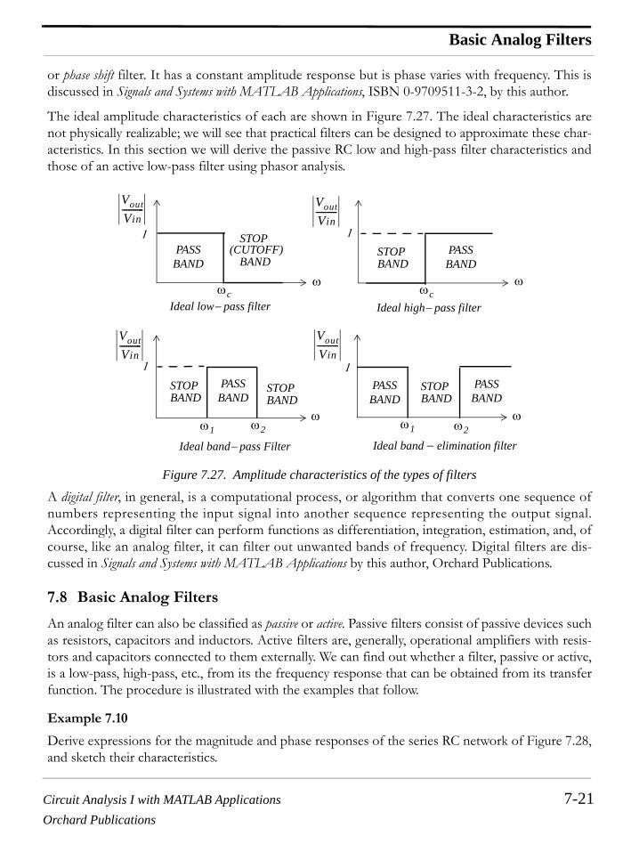
Circuit Analysis I with MATLAB Applications 7-21Orchard Publications
Basic Analog Filters
or phase shift filter. It has a constant amplitude response but is phase varies with frequency. This isdiscussed in Signals and Systems with MATLAB Applications, ISBN 0-9709511-3-2, by this author.
The ideal amplitude characteristics of each are shown in Figure 7.27. The ideal characteristics arenot physically realizable; we will see that practical filters can be designed to approximate these char-acteristics. In this section we will derive the passive RC low and high-pass filter characteristics andthose of an active low-pass filter using phasor analysis.
Figure 7.27. Amplitude characteristics of the types of filters
A digital filter, in general, is a computational process, or algorithm that converts one sequence ofnumbers representing the input signal into another sequence representing the output signal.Accordingly, a digital filter can perform functions as differentiation, integration, estimation, and, ofcourse, like an analog filter, it can filter out unwanted bands of frequency. Digital filters are dis-cussed in Signals and Systems with MATLAB Applications by this author, Orchard Publications.
7.8 Basic Analog Filters
An analog filter can also be classified as passive or active. Passive filters consist of passive devices suchas resistors, capacitors and inductors. Active filters are, generally, operational amplifiers with resis-tors and capacitors connected to them externally. We can find out whether a filter, passive or active,is a low-pass, high-pass, etc., from its the frequency response that can be obtained from its transferfunction. The procedure is illustrated with the examples that follow.
Example 7.10
Derive expressions for the magnitude and phase responses of the series RC network of Figure 7.28,and sketch their characteristics.
PASSBAND
STOP
BAND
Ideal low− pass filter Ideal high− pass filter
(CUTOFF)
BAND STOP
PASSBAND
PASSBAND
Ideal band− pass Filter Ideal band − elimination filter
BAND STOP
BAND STOP
PASSBAND
PASSBAND BAND
STOP
1
11
1
VoutVin---------- Vout
Vin----------
VoutVin----------
VoutVin----------
ωcω ω
ω ω
ωc
ω1 ω1ω2 ω2
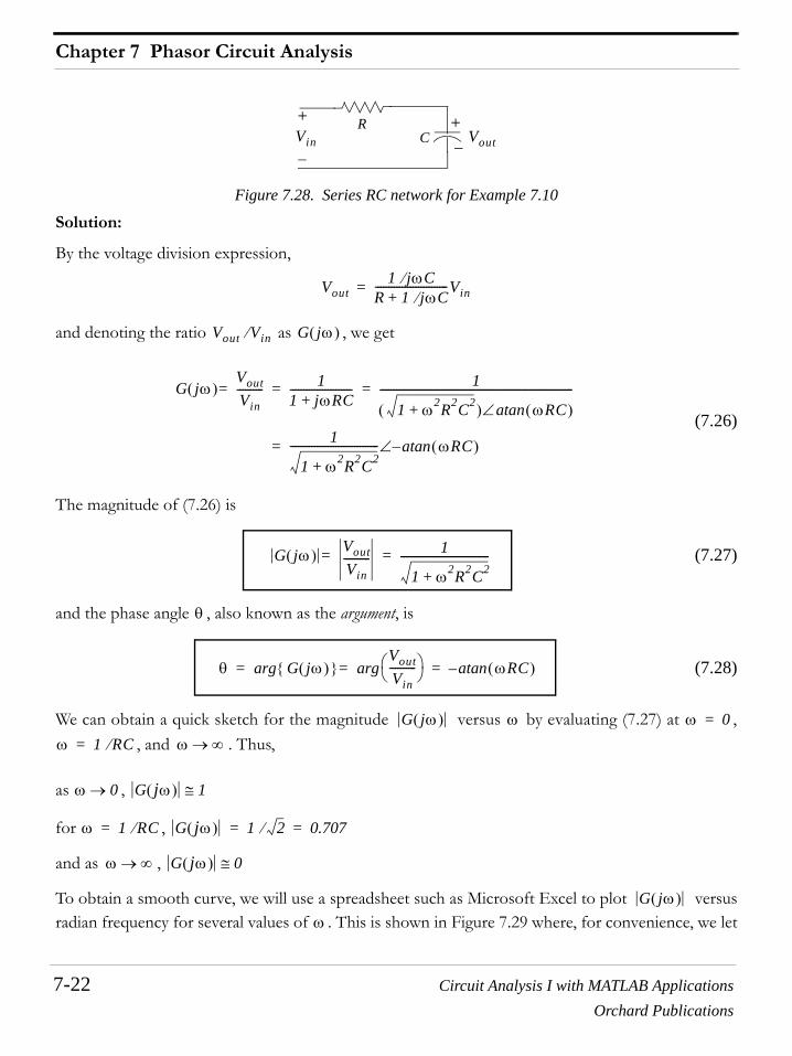
Chapter 7 Phasor Circuit Analysis
7-22 Circuit Analysis I with MATLAB ApplicationsOrchard Publications
Figure 7.28. Series RC network for Example 7.10
Solution:
By the voltage division expression,
and denoting the ratio as , we get
(7.26)
The magnitude of (7.26) is
(7.27)
and the phase angle , also known as the argument, is
(7.28)
We can obtain a quick sketch for the magnitude versus by evaluating (7.27) at ,, and . Thus,
as ,
for ,
and as ,
To obtain a smooth curve, we will use a spreadsheet such as Microsoft Excel to plot versusradian frequency for several values of . This is shown in Figure 7.29 where, for convenience, we let
+
−
RCVin Vout
+−
Vout1 jωC⁄
R 1 jωC⁄+---------------------------Vin=
Vout Vin⁄ G jω( )
G jω( )VoutVin----------= 1
1 jωRC+----------------------- 1
1 ω2R2C2+( ) ωRC( )atan∠------------------------------------------------------------------------= =
1
1 ω2R2C2+--------------------------------- ωRC( )atan–∠=
G jω( ) VoutVin----------= 1
1 ω2R2C2+---------------------------------=
θ
θ G jω( ) VoutVin----------⎝ ⎠
⎛ ⎞arg=arg ωRC( )atan–= =
G jω( ) ω ω 0=
ω 1 RC⁄= ω ∞→
ω 0→ G jω( ) 1≅
ω 1 RC⁄= G jω( ) 1 2⁄ 0.707= =
ω ∞→ G jω( ) 0≅
G jω( )ω

Circuit Analysis I with MATLAB Applications 7-23Orchard Publications
Basic Analog Filters
. The plot shows that this circuit is an approximation, although not a good one, to theamplitude characteristics of a low-pass filter.
Figure 7.29. Amplitude characteristics of a series RC low-pass filter
We can also obtain a quick sketch for the phase angle, i.e., versus by evaluating
of (11.3) at , , , and . Thus,
as ,
for ,
for ,
as ,
and as ,
We use Excel to plot versus radian frequency for several values of . This is shown in Figure7.31 where, again for convenience, we let
Example 7.11
The network of Figure 7.30 is also a series RC circuit, where the positions of the resistor and capac-itor have been interchanged. Derive expressions for the magnitude and phase responses, and sketchtheir characteristics.
Figure 7.30. RC network for Example 7.11
RC 1=
ω |G(jω)|0.000 10.020 0.99980.040 0.99920.060 0.99820.080 0.996820.100 0.995040.120 0.992880.140 0.990340.160 0.987440.180 0.984180.200 0.980580.220 0.97664
Series RC Low-pass Filter Frequency Response
0
0.2
0.4
0.6
0.8
1
Radian Frequency (ω)
|G(j ω
)|
Half-power point
1/RC
(|G(jω)|=0.707)
RC=1
θ G jω( ) arg= ω
ω 0= ω 1 RC⁄= ω 1– RC⁄= ω ∞–→ ω ∞→
ω 0→ θ 0atan– 0°≅ ≅
ω 1 RC⁄= θ 1atan– 45°–= =
ω 1– RC⁄= θ 1–( )atan– 45°= =
ω ∞–→ θ ∞–( )atan– 90°= =
ω ∞→ θ ∞( )atan– 90– °= =
θ ωRC 1=
+
−R
CVin
Vout
+
−
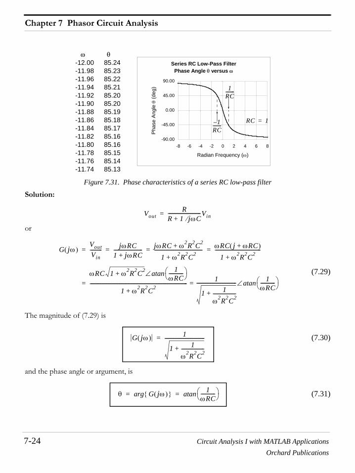
Chapter 7 Phasor Circuit Analysis
7-24 Circuit Analysis I with MATLAB ApplicationsOrchard Publications
Figure 7.31. Phase characteristics of a series RC low-pass filter
Solution:
or
(7.29)
The magnitude of (7.29) is
(7.30)
and the phase angle or argument, is
(7.31)
ω θ-12.00 85.24-11.98 85.23-11.96 85.22-11.94 85.21-11.92 85.20-11.90 85.20-11.88 85.19-11.86 85.18-11.84 85.17-11.82 85.16-11.80 85.16-11.78 85.15-11.76 85.14-11.74 85.13
Series RC Low-Pass Filter Phase Angle θ versus ω
-90.00
-45.00
0.00
45.00
90.00
-8 -6 -4 -2 0 2 4 6 8
Radian Frequency (ω)P
hase
Ang
le θ
(deg
)
RC 1=
1RC--------
1–RC--------
VoutR
R 1 jωC⁄+---------------------------Vin=
G jω( )VoutVin---------- jωRC
1 jωRC+------------------------ jωRC ω2R2C2+
1 ω2R2C2+---------------------------------------- ωRC j ωRC+( )
1 ω2R2C2+--------------------------------------= = = =
ωRC 1 ω2R2C2+1
ωRC------------⎝ ⎠
⎛ ⎞atan∠
1 ω2R2C2+--------------------------------------------------------------------------------- 1
1 1ω2R2C2-------------------+
--------------------------------- 1ωRC------------⎝ ⎠
⎛ ⎞atan∠==
G jω( ) 1
1 1ω2R2C2-------------------+
---------------------------------=
θ G jω( ) arg 1ωRC------------⎝ ⎠
⎛ ⎞atan= =

Circuit Analysis I with MATLAB Applications 7-25Orchard Publications
Basic Analog Filters
We can obtain a quick sketch for the magnitude versus by evaluating (7.30) at ,, and . Thus,
as ,
for ,
and as ,
Figure 7.32 shows versus radian frequency for several values of where . Theplot shows that this circuit is an approximation, although not a good one, to the amplitude charac-teristics of a high-pass filter.
Figure 7.32. Amplitude characteristics of a series RC high-pass filter
We can also obtain a quick sketch for the phase angle, i.e., versus , by evaluat-ing (7.31) at , , , , and . Thus,
as ,
for , for ,
as ,
and as ,
Figure 7.33 shows the phase angle versus radian frequency for several values of , where
G jω( ) ω ω 0=
ω 1 RC⁄= ω ∞→
ω 0→ G jω( ) 0≅
ω 1 RC⁄= G jω( ) 1 2⁄ 0.707= =
ω ∞→ G jω( ) 1≅
G jω( ) ω RC 1=
ω |G(jω)|0.000 1E-070.020 0.020.040 0.039970.060 0.059890.080 0.079750.100 0.09950.120 0.119150.140 0.138650.160 0.157990.180 0.177150.200 0.196120.220 0.21486
Series RC High-Pass Filter |G(jω)| versus ω
0
0.2
0.4
0.6
0.8
1
Radian Frequency (ω)
|G(j ω
)|
Half-power point
1/RC
(|G(jω)|=0.707)
RC=1
θ G jω( ) arg= ω
ω 0= ω 1 RC⁄= ω 1– RC⁄= ω ∞–→ ω ∞→
ω 0→ θ 0atan– 0°≅ ≅
ω 1 RC⁄= θ 1atan– 45°–= =
ω 1– RC⁄= θ 1–( )atan– 45°= =
ω ∞–→ θ ∞–( )atan– 90°= =
ω ∞→ θ ∞( )atan– 90– °= =
θ ωRC 1=

Chapter 7 Phasor Circuit Analysis
7-26 Circuit Analysis I with MATLAB ApplicationsOrchard Publications
Figure 7.33. Phase characteristics of an RC high-pass filter
7.9 Active Filter Analysis
We can analyze active filters, such as those we discussed in Chapter 4, using phasor circuit analysis.
Example 7.12
Compute the approximate cut-off frequency of the circuit of Figure 7.34 which is known as a Multi-ple Feed Back (MFB) active low-pass filter.
Figure 7.34. Low-pass filter for Example 7.12
Solution:
We write the phasor circuit nodal equations as follows:
At Node :
(7.32)
ω θ-12.000 -4.7636417-11.980 -4.7715577-11.960 -4.7794999-11.940 -4.7874686-11.920 -4.7954638-11.900 -4.8034858-11.880 -4.8115345-11.860 -4.8196102-11.840 -4.827713-11.820 -4.835843-11.800 -4.8440004-11.780 -4.8521853-11.760 -4.8603978-11.740 -4.8686381
Series RC High-pass Filter Phase Angle θ versus ω
-90
-45
0
45
90
-8 -6 -4 -2 0 2 4 6 8
Radian Frequency (ω)P
hase
Ang
le θ
(deg
)
RC=1
25 nF
10 nF
vin vout
v1 v2
50 kΩ
R1
R2
R3
C2
C1
40 kΩ
200 kΩ
v1 vin–
R1------------------
v11 jωC1( )⁄------------------------
v1 vout–
R2---------------------
v1 v2–
R3----------------+ + + 0=

Circuit Analysis I with MATLAB Applications 7-27Orchard Publications
Active Filter Analysis
At node :
(7.33)
and since (virtual ground), relation (7.33) reduces to
(7.34)
and by substitution of (7.34) into (7.32), rearranging, and collecting like terms, we get:
(7.35)
or
(7.36)
By substitution of given values of resistors and capacitors, we get
or
(7.37)
and now we can use MATLAB to find and plot the magnitude of (7.37) with the following code.
w=1:10:10000; Gjw=−1./(2.5.*10.^(−6).*w.^2−5.*j.*10.^(−3).*w+5);semilogx(w,abs(Gjw)); grid; hold onxlabel('Radian Frequency w'); ylabel('|Vout/Vin|');title('Magnitude Vout/Vin vs. Radian Frequency')
The plot is shown in Figure 7.35 where we see that the cutoff frequency occurs at about. We observe that the half-power point for this plot is .
v2 v1–
R3----------------
C21 jωC2( )⁄------------------------=
v2 0=
v1 jωR– 3C2( )vout=
1R1------ 1
R2------ 1
R3------ jωC1+ + +⎝ ⎠
⎛ ⎞ jωR– 3C2( ) 1R2------– vout
1R1------vin=
voutvin---------- 1
R11
R1------ 1
R2------ 1
R3------ jωC1+ + +⎝ ⎠
⎛ ⎞ jωR– 3C2( ) 1R2------–
----------------------------------------------------------------------------------------------------------------=
voutvin---------- 1
2 10 5× 120 10 3×--------------------- j2.5 10 8–× ω+⎝ ⎠
⎛ ⎞ j5 10 4× 10 8–× ω–( ) 14 10 4×------------------–
-----------------------------------------------------------------------------------------------------------------------------------------------------------------------=
G jω( )voutvin---------- 1–
2.5 10 6–× ω2 j5 10 3–× ω 5+–-------------------------------------------------------------------------==
700 rad s⁄ 0.2 0.707× 0.141=

Chapter 7 Phasor Circuit Analysis
7-28 Circuit Analysis I with MATLAB ApplicationsOrchard Publications
Figure 7.35. Plot for the magnitude of the low-pass filter circuit of Example 7.12
7.10 Summary
• In Chapter 3 we were concerned with constant voltage and constant current sources, resistancesand conductances. In this chapter we were concerned with alternating voltage and alternating cur-rent sources, impedances, and admittances.
• Nodal analysis, mesh analysis, the principle of superposition, Thevenin’s theorem, and Norton’stheorem can also be applied to phasor circuits.
• The use of complex numbers make the phasor circuit analysis much easier.
• MATLAB can be used very effectively to perform the computations since it does not require anyspecial procedures for manipulation of complex numbers.
• Whenever a branch in a circuit contains two or more devices in series or two or more devices inparallel, it is highly recommended that they are grouped and denoted as , , and so on beforewriting nodal or mesh equations.
• Phasor diagrams are sketches that show the magnitude and phase relationships among several pha-sor voltages and currents. When constructing a phasor diagram, the first step is to select one pha-sor as a reference, usually with zero phase angle, and all other phasors must be drawn with the cor-rect relative angles.
• The RC low-pass and RC high-pass filters are rudimentary types of filters and are not used in prac-tice. They serve as a good introduction to electric filters.
100
101
102
103
104
0
0.02
0.04
0.06
0.08
0.1
0.12
0.14
0.16
0.18
0.2Magnitude Vout/Vin vs. Radian Frequency
|Vou
t/V
in|
Radian Frequency w
z1 z2

Circuit Analysis I with MATLAB Applications 7-29Orchard Publications
Exercises
7.11 Exercises
Multiple Choice
1. In the circuit of Figure 7.36 the phasor voltage is
A.
B.
C.
D.
E. none of the above
Figure 7.36. Circuit for Question 1
2. In the circuit of Figure 7.37 the phasor current is
A.
B.
C.
D.
E. none of the above
Figure 7.37. Circuit for Question 2
3. In the circuit of Figure 7.38 the voltage across the capacitor is
A.
B.
V
2 j0 V+
1 j0 V+
1 j– 0 V
1 j V+
IS +
−
−j ΩV
1 0° A∠
1 Ω
j0.5 Ω
I
0 j2 A+
0 j2 A–
1 j0 A+
2 j2 A+
VS
−j1 Ω2 0° V∠
1 Ω
j1 Ω
1 Ω1 ΩI
C2
8 10 4– 2000t 90°+( ) Vsin×
50 2000t 45°–( ) Vcos

Chapter 7 Phasor Circuit Analysis
7-30 Circuit Analysis I with MATLAB ApplicationsOrchard Publications
C.
D.
E. none of the above
Figure 7.38. Circuit for Question 3
4. In the circuit of Figure 7.39 the current through the capacitor is
A.
B.
C.
D.
E. none of the above
Figure 7.39. Circuit for Question 4
5. The Thevenin equivalent voltage at terminals A and B in the circuit of Figure 7.40 is
A.
B.
C.
D.
E. none of the above
50 2000t 45°+( ) Vcos
50 2000t 90°+( ) Vcos
4 Ω
8 2000t 90°+( )sin
vS t( )
L1
C2
C1
L23 mH2 mH500 µF
100 µF
iC t( )
4 2000tsin
4 2000t 180°+( )sin
32 2000t 45°–( )cos
32 2000t 90°+( )cos
1 Ω
iC
iS t( ) 4 2000tcos=
0.5 mH500 µF
iS t( )
VTH
10 90° V–∠
10 53.13° V–∠
10 53.13° V∠
10 45° V–∠

Circuit Analysis I with MATLAB Applications 7-31Orchard Publications
Exercises
Figure 7.40. Circuit for Questions 5 and 6
6. The Thevenin equivalent impedance at terminals A and B in the circuit of Figure 7.40 is
A.
B.
C.
D.
E. none of the above
7. In the circuit of Figure 7.41 the phasor voltage is
A.
B.
C.
D.
E. none of the above
Figure 7.41. Circuit for Question 7
8. In the circuit of Figure 7.42 the phasor voltage is
A.
B.
VS
−j5 Ω10 0° V∠
4 Ω j2 ΩA
B
ZTH
2 j4 Ω+
4 j2 Ω+
4 j– 2 Ω
j– 5 Ω
VC
5 90° –∠ V
5 45° –∠ V
4 53.1° –∠ V
4 53.1° ∠ V
VS
− −j4 Ω20 0° V∠ j3 Ω
+ +−
4 ΩIX IX
4IX V
VR5 Ω
20 j0 V+
0 j20 V+

Chapter 7 Phasor Circuit Analysis
7-32 Circuit Analysis I with MATLAB ApplicationsOrchard Publications
C.
D.
E. none of the above
Figure 7.42. Circuit for Question 8
9. In the circuit of Figure 7.43 the phasor voltage is
A.
B.
C.
D.
E. none of the above
Figure 7.43. Circuit for Question 9
10. In the circuit of Figure 7.44 the voltage is
A.
B.
C.
D.
20 j20 V+
80 j80– V
IS
−4 0° A∠
j4 Ω
+
4 Ω
2VX A
VX 5 Ω
+
−VR5 Ω
VOUT 2
2 j0 V+
4 j0 V+
4 j– 0 V
1 j1 V+
10 Ω
−
10 Ω
VOUT 1
VIN
1 0°∠VOUT 2
j5 Ωj– 5 Ω
t domain– vAB t( )
1.89 ωt 45°+( ) Vcos
0.53 ωt 45– °( ) Vcos
2 ωt Vcos
0.5 ωt 53.1°+( ) Vcos

Circuit Analysis I with MATLAB Applications 7-33Orchard Publications
Exercises
E. none of the above
Figure 7.44. Circuit for Question 10
Problems
1. For the circuit of Figure 7.45, . Compute and .
Figure 7.45. Circuit for Problem 1
2. Write nodal equations and use MATLAB to compute for the circuit of Figure 7.46 giventhat .
Figure 7.46. Circuit for Problem 2
3. Write mesh equations and use MATLAB to compute for the circuit of Figure 7.47 giventhat .
VS j2 Ω
−j Ω
2 Ω
2 0° V∠
2 Ω
A
B
iS t( ) 2 1000t Acos= vAB t( ) iC t( )
8 Ω
A
6 Ω
5 Ω
7 Ω
20 mH
2 Ω
B
iC t( )
iS t( )
1000 6⁄ µF
iC t( )
vS t( ) 12 1000t 45°+( ) Vcos=
4 Ω10 Ω 5 Ω
20 Ω 5 mH
2 Ω
100 µF
+
−
vS t( )
iC t( )
iL t( )
vS t( ) 100 10000t 60°+( ) Vcos=

Chapter 7 Phasor Circuit Analysis
7-34 Circuit Analysis I with MATLAB ApplicationsOrchard Publications
Figure 7.47. Circuit for Problem 3
4. For the circuit of Figure 7.48, it is given that and. Use superposition to find .
Figure 7.48. Circuit for Problem 4
5. For the circuit of Figure 7.49, find if , , and. Plot using MATLAB or Excel.
Figure 7.49. Circuit for Problem 5
6. For the circuit of Figure 7.50, find the value of which will receive maximum power.
4 Ω10 Ω 5 Ω
20 Ω2 mH
2 Ω
10 µF
+
− vS t( )iL t( )
vS1 t( ) 40 5000t 60°+( ) Vcos=
vS2 t( ) 60 5000t 60°+( ) Vsin= vC t( )
+
−
25 Ω10 Ω+
−
+
−20 µF
5 mH2 mH
vC t( )
vS1 t( )vS2 t( )
R2R1 L2L1
vC t( ) vS1 15 V= vS2 t( ) 20 1000t Vcos=
iS t( ) 4 2000t Acos= vC t( )
+
− 5 Ω
10 Ω
+− 500 µF
2 mH1 mH
+
−
vC t( )
vS2 t( )
iS t( )
vS1
ZLD
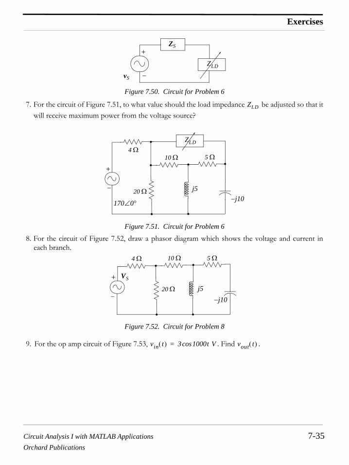
Circuit Analysis I with MATLAB Applications 7-35Orchard Publications
Exercises
Figure 7.50. Circuit for Problem 6
7. For the circuit of Figure 7.51, to what value should the load impedance be adjusted so that itwill receive maximum power from the voltage source?
Figure 7.51. Circuit for Problem 6
8. For the circuit of Figure 7.52, draw a phasor diagram which shows the voltage and current ineach branch.
Figure 7.52. Circuit for Problem 8
9. For the op amp circuit of Figure 7.53, . Find .
vS
+
−
ZS
ZLD
ZLD
4 Ω10 Ω 5 Ω
20 Ω
+
− j5
−j10170 0°∠
ZLD
4 Ω 10 Ω 5 Ω
20 Ω
+
−j5
−j10
VS
vin t( ) 3 1000t Vcos= vout t( )
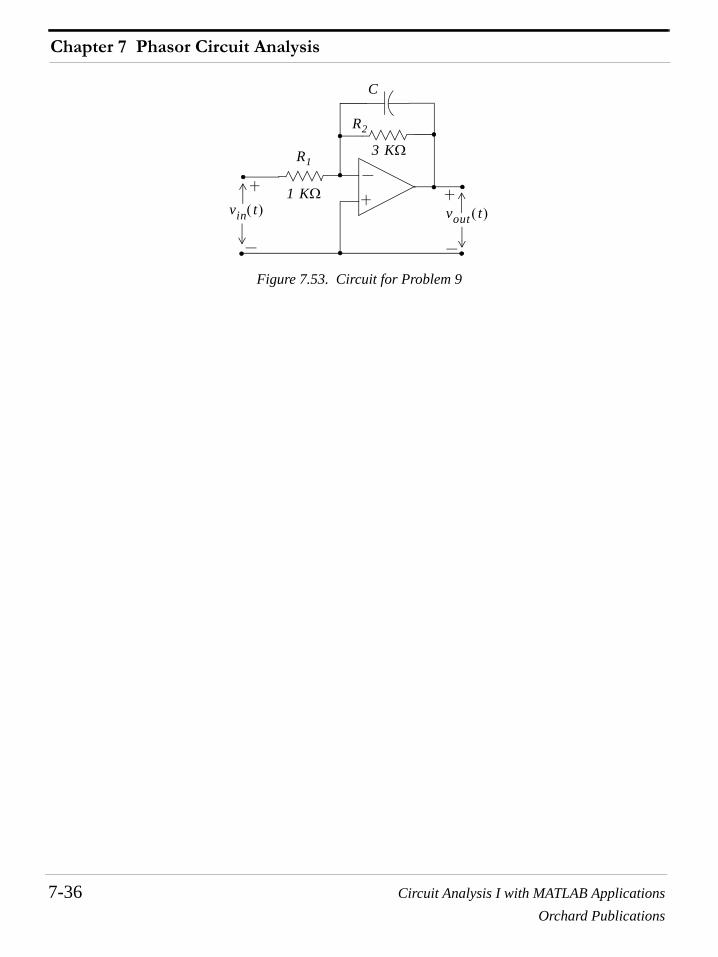
Chapter 7 Phasor Circuit Analysis
7-36 Circuit Analysis I with MATLAB ApplicationsOrchard Publications
Figure 7.53. Circuit for Problem 9
vout t( )vin t( )1 KΩ
R2
R1
C
3 KΩ

Circuit Analysis I with MATLAB Applications 7-37Orchard Publications
Answers to Exercises
7.12 Answers to Exercises
Multiple Choice
1. E where and is found from the nodal equa-
tion or or . Therefore,
2. C Denoting the resistor in series with the voltage source as , the resistor in series with thecapacitor as , and the resistor in series with the capacitor as , the equivalent impedance is
and
3. B , , , , and the phasor equivalent circuit is shown below.
, ,
and thus
4. D , , , , and the pha-sor equivalent circuit is shown below.
V VL VC+= VL 1 0°∠ j1 2⁄× j1 2⁄ V= = VC
VC1
-------VC
j–-------+ 1 j0+= 1 j+( )VC 1= VC
11 j+----------- 1 j–
1 j–----------× 1 j–
2---------- 1
2--- j12
--- V–= ==
V j1 2⁄ 1 2⁄ j1 2⁄–+ 1 2⁄ j0 V+= =
z1
z2 z3
Zeq z1z2 z3⋅z2 z3+---------------+ 1 1 j1–( ) 1 j1+( )
1 j1– 1 j1+ +--------------------------------------+ 1 2
2---+ 2 j0+= = = =
IVSZ
------ 2 j0+2 j0+-------------- 1 j0 A+= = =
8 2000t 90°+( )sin 8 2000t 8 0° V∠⇔cos= jωL1 j6= jωL2 j4= j– ωC1⁄ j1–=
j– ωC1⁄ j1–=
VS
−j5 Ω8 0° V∠
4 Ω j6 Ω
L1
C2
C1
L2
j4 Ω−j1 Ω
I
+
−
Z 4 j6 j1– j4 j5–+ + 4 j4+= = IVSZ
------ 8 j0+4 j4+-------------- 8 j0+
4 j4+-------------- 4 j4–
4 j4–--------------⋅ 32 j32–
32-------------------- 1 j1–= = = = =
VC2j5– 1 j–( )× 5 j5– 50 45°–∠ 50 2000t 45°–( ) Vcos⇔= = =
4 2000t 4 0°∠⇔cos G 1 R⁄ 1 Ω 1–= = jωC j1 Ω 1–= j– ωL⁄ j1 Ω 1––=
IS
4 0° A∠
IC 1 Ω 1–
j1 Ω 1––
j1 Ω 1–

Chapter 7 Phasor Circuit Analysis
7-38 Circuit Analysis I with MATLAB ApplicationsOrchard Publications
Denoting the parallel combination of the conductance and inductance as andusing the current division expression for admittances we get
and thus
5. B By the voltage division expression
6. C We short the voltage source and looking to the left of points A and B we observe that thecapacitor is in parallel with the series combination of the resistance and inductance. Thus,
7. D ,
and
8. E
and
9. B
and
10. A We write the nodal equation at Node A for as
Y1 1 j1–=
ICjωC
jωC Y1+---------------------- IS⋅ j1
j1 1 j1–+------------------------- j1 4 0°∠× 1 90°∠ 4 0°∠× 4 90° A∠= = = = =
iS t( ) 4 2000t 90°+( ) Acos=
VTH VABj5–
4 j2 j5–+------------------------- 10 0°∠⋅ 5 90°–∠ 10 0°∠×
4 j3–------------------------------------------ 50 90°–∠
5 36.9°–∠------------------------ 10 53.1° V–∠= = = = =
ZTHj5–( ) 4 j2+( )
4 j2 j5–+-------------------------------- 10 j20–
4 j3–-------------------- 10 j20–
4 j3–-------------------- 4 j3+
4 j3+--------------⋅ 100 j50–
25----------------------- 4 j2–= = = = =
IX20 0°∠4 j3+---------------- 20 0°∠
5 36.9°∠--------------------- 4 36.9°–∠= = = 4IX 16 36.9°–∠=
IC4IX
j4–-------- 16 36.9°–∠
4 90°–∠--------------------------- 4 53.1°∠= = =
VX4
4 j4+-------------- 4 0°∠× j4× 64 90°∠
32 45°∠----------------------- 64 32×
32---------------------- 45° 2 32 45°∠=∠= = =
VR5 Ω2VX 5× 20 32 45°∠× 20 32 2
2------- j 2
2-------+⎝ ⎠
⎛ ⎞ 80 j80+= = = =
VOUT 110j5------ 1 0°∠×– j2 1 0°∠× 2 90°∠ 1 0°∠× 2 90°∠= = = =
VOUT 210j– 5
-------- VOUT 1×– j– 2 2 0°∠× 2 90– °∠ 2 90°∠× 4 0°∠ 4 j0+= = = = =
VAB

Circuit Analysis I with MATLAB Applications 7-39Orchard Publications
Answers to Exercises
or and in the
Problems
1. We transform the current source and its parallel resistance to a voltage source series resistance,we combine the series resistors, and we draw the phasor circuit below.
For this phasor circuit, , and
, , , and
We observe that and . At Node A,
and
VAB 2 0°∠–
j–-----------------------------
VAB2
---------VAB
2 j2+--------------+ + 0=
12--- j 1
2 j2+--------------+ +⎝ ⎠
⎛ ⎞ VAB 2 90°∠=
VAB2 90°∠
1 2⁄ j 1 4⁄ j 4⁄–+ +------------------------------------------------- 2 90°∠
3 4⁄ j3 4⁄+---------------------------- 2 90°∠
1.06 45°∠------------------------= = =
VAB 1.89 45°∠= t domain– vAB t( ) 1.89 ωt 45°+( )cos=
8 Ω
A
6 Ω
5 Ω
15 Ω8 Ω
B
+
−
VS
j6 Ω–
IC
j20 Ω
10 0° V∠
C
z1z2 z3
VS 2 0°∠ 5× 10 0° V∠= = jωL j103 20 10 3–×× j20 Ω= =
j– ωC⁄ j 103 103 6⁄× 10 6–×( )⁄– j6–= = z1 5 Ω= z2 15 j20+( ) Ω= z3 8 j– 6( ) Ω=
VA VAB VAC VCB+ VAC 10 0° V∠+= = = VB 0=
VA VB–
z2-------------------
VA 10 0°∠–
z1-----------------------------
VA VB–
z3-------------------+ + 0=
1z1---- 1
z2---- 1
z3----+ +⎝ ⎠
⎛ ⎞ VA10 0°∠
z1----------------=
15--- 1
15 j20+-------------------- 1
8 j– 6-----------+ +⎝ ⎠
⎛ ⎞ VA10 0°∠
5---------------- 2 0°∠= =
Chapter 7 Phasor Circuit Analysis
7-40 Circuit Analysis I with MATLAB ApplicationsOrchard Publications
Then, in the .
Also,
and
Check with MATLAB:
z1=5; z2=15+20j; z3=8−6j; VA=(10+0j)/(z1*(1/z1+1/z2+1/z3)); fprintf(' \n');...fprintf('magVA = %5.2f V \t',abs(VA));...fprintf('phaseVA = %5.2f deg \t',angle(VA)*180/pi); fprintf(' \n'); fprintf(' \n');
magVA = 6.55 V phaseVA = -5.26 deg
2. The equivalent phasor circuit is shown below where and
Node :
VA2 0°∠
0.2 125 53.1°∠------------------------ 1
10 36.9°–∠---------------------------+ +
------------------------------------------------------------------------ 2 0°∠0.2 0.04 53.1– °∠ 0.1 36.9°∠+ +------------------------------------------------------------------------------= =
2 0°∠0.2 0.04 53.1° j0.04 53.1° 0.1 36.9° j0.1 36.9°sin+cos+sin–cos+-----------------------------------------------------------------------------------------------------------------------------------------------------------------=
2 0°∠0.2 0.04 0.6× j0.04 0.8×– 0.1 0.8 j0.1 0.6×+×++------------------------------------------------------------------------------------------------------------------------------ 2 0°∠
0.304 j0.028+-----------------------------------==
2 0°∠0.305 5.26°∠------------------------------- 6.55 5.26°–∠==
t domain– vAB t( ) 6.55 1000 5.26°+( )cos=
ICVAz3------ 6.55 5.26°–∠
10 36.9°–∠------------------------------- 0.655 31.7°∠= = =
iC t( ) 0.655 1000 31.7°+( )cos=
jωL j103 5 10 3–×× j5= =
j– ωC⁄ j 103 10 4–×( )⁄– j10–= =
4 Ω
10 Ω 5 Ω
20 Ω
2 Ω
+
−
V2V1 V3VS
12 45°∠
z1
z2
z3
z4
z5
z6
IC
z7
j5 Ωj– 10 Ω
V1
V1 VS–
z1------------------
V1 V2–
z3------------------
V1z2------
V1 V3–
z7------------------+ + +

Circuit Analysis I with MATLAB Applications 7-41Orchard Publications
Answers to Exercises
or
Node :
or
Node :
or
and in matrix form
Shown below is the MATLAB code to solve this system of equations.
Vs=12*(cos(pi/4)+j*sin(pi/4)); % Express Vs in rectangular formz1=4; z2=20; z3=10; z4=5j; z5=5; z6=−10j; z7=2;...Y=[1/z1+1/z2+1/z3+1/z7 −1/z3 −1/z7;...−1/z3 1/z3+1/z4+1/z5 −1/z5;...−1/z7 −1/z5 1/z5+1/z6+1/z7];...I=[Vs/z1 0 0]'; V=Y\I; Ic=V(3)/z6;...magIc=abs(Ic); phaseIc=angle(Ic)*180/pi;...disp('V1='); disp(V(1)); disp('V2='); disp(V(2));...disp('V3='); disp(V(3)); disp('Ic='); disp(Ic);...format bank % Display magnitude and angle values with two decimal placesdisp('magIc='); disp(magIc); disp('phaseIc='); disp(phaseIc);...fprintf(' \n');
V1 = 5.9950 - 4.8789i
1z1---- 1
z2---- 1
z3---- 1
z7----+ + +⎝ ⎠
⎛ ⎞ V11z3----V2–
1z7----V3–
1z1----VS=
V2
V2 V1–
z3------------------
V2z4------
V2 V3–
z5------------------+ + 0=
1z3----V1
1z3---- 1
z4---- 1
z5----+ +⎝ ⎠
⎛ ⎞ V2+–1z5----V3– 0=
V3
V3 V2–
z5------------------
V3 V1–
z7------------------
V2 V3–
z6------------------+ + 0=
1z7----V1
1z5----V2– 1
z5---- 1
z6---- 1
z7----+ +⎝ ⎠
⎛ ⎞ V3+– 0=
1z1---- 1
z2---- 1
z3---- 1
z7----+ + +⎝ ⎠
⎛ ⎞ 1z3----– 1
z7----–
1z3----– 1
z3---- 1
z4---- 1
z5----+ +⎝ ⎠
⎛ ⎞ 1z5----–
1z7----– 1
z5----– 1
z5---- 1
z6---- 1
z7----+ +⎝ ⎠
⎛ ⎞
V1
V2
V3
⋅
1z1----VS
00
=

Chapter 7 Phasor Circuit Analysis
7-42 Circuit Analysis I with MATLAB ApplicationsOrchard Publications
V2 = 5.9658 - 0.5960i
V3 = 5.3552 - 4.4203i
Ic = 0.4420 + 0.5355i
magIc = 0.69
phaseIc = 50.46
Therefore,
3. The equivalent phasor circuit is shown below where and
Mesh :
Mesh :
Mesh :
Mesh :
and in matrix form
IC 0.69 50.46° iC t( )⇔∠ 0.69 1000t 50.46°+( ) Acos= =
jωL j104 2 10 3–×× j20= =
j– ωC⁄ j 104 10× 10 6–×( )⁄– j10–= =
4 Ω
10 Ω 5 Ω
20 Ω
2 Ω
+
−
j10 Ω–
j20 Ω
VS 100 60°∠=
IL
z7
z2
z1
z3
z4
z6
z5
I1
I2
I3
I4
I1
z1 z2+( )I1 z2I3– VS=
I2
z1 z2 z7+ +( )I2 z3I3 z5I4–– 0=
I3
z2I1 z3I2–– z2 z3 z4+ +( )I3 z4I4–+ 0=
I4
z5I2 z4I3–– z4 z5 z6+ +( )I4+ 0=
Circuit Analysis I with MATLAB Applications 7-43Orchard Publications
Answers to Exercises
Shown below is the MATLAB code to solve this system of equations.
Vs=100*(cos(pi/3)+j*sin(pi/3)); % Express Vs in rectangular formz1=4; z2=20; z3=10; z4=20j; z5=5; z6=−10j; z7=2;...Z=[z1+z2 0 −z2 0;...0 z3+z5+z7 −z3 −z5;...−z2 −z3 z2+z3+z4 −z4;...0 −z5 −z4 z4+z5+z6];...V=[Vs 0 0 0]'; I=Z\V; IL=I(3)−I(4);...magIL=abs(IL); phaseIL=angle(IL)*180/pi;...disp('I1='); disp(I(1)); disp('I2='); disp(I(2));...disp('I3='); disp(I(3)); disp('I4='); disp(I(4));...disp('IL='); disp(IL);...format bank % Display magnitude and angle values with two decimal placesdisp('magIL='); disp(magIL); disp('phaseIL='); disp(phaseIL);...fprintf(' \n');
I1 = 5.4345 - 3.4110i
I2 = 4.5527 + 0.7028i
I3 = 4.0214 + 0.2369i
I4 = 7.4364 + 1.9157i
IL= -3.4150- 1.6787i
magIL = 3.81
phaseIL = -153.82
Therefore,
4. The equivalent phasor circuit is shown below where
z1 z2+ 0 z2– 00 z1 z2 z7+ + z3– z5–
z2– z3– z2 z3 z4+ + z4–
0 z5– z4– z4 z5 z6+ +
I1
I2
I3
I4
⋅
VS
000
=
IL 3.81 153.82°–∠= iL t( )⇔ 3.81 104t 153.82°––( )cos=
jωL1 j5 103× 2 10 3–×× j10= =
jωL2 j5 103× 5 10 3–×× j25= =
j– ωC⁄ j 5 103× 20× 10 6–×( )⁄– j10–= =
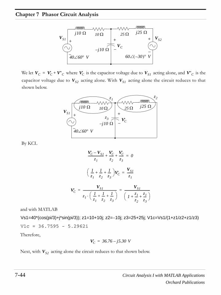
Chapter 7 Phasor Circuit Analysis
7-44 Circuit Analysis I with MATLAB ApplicationsOrchard Publications
We let where is the capacitor voltage due to acting alone, and is thecapacitor voltage due to acting alone. With acting alone the circuit reduces to thatshown below.
By KCL
and with MATLAB
Vs1=40*(cos(pi/3)+j*sin(pi/3)); z1=10+10j; z2=−10j; z3=25+25j; V1c=Vs1/(1+z1/z2+z1/z3)
V1c = 36.7595 - 5.2962i
Therefore,
Next, with acting alone the circuit reduces to that shown below.
+
−
25 Ω10 Ω+
−
+
−
VC
j10 Ω j25 Ω
j– 10 Ω
VS1 VS2
40 60° ∠ V 60 30–( )° ∠ V
VC V'C V''C+= V'C VS1 V''CVS2 VS1
+
−
25 Ω10 Ω
+
−
V'C
j10 Ω j25 Ω
j– 10 Ω
VS1
40 60° ∠ V
z1z2
z3
V'C VS1–
z1---------------------
V'Cz2------
V'Cz3------+ + 0=
1z1---- 1
z2---- 1
z3----+ +⎝ ⎠
⎛ ⎞ V'CVS1z1
--------=
V'CVS1
z11z1---- 1
z2---- 1
z3----+ +⎝ ⎠
⎛ ⎞⋅---------------------------------------------
VS1
1z1z2----
z1z3----+ +⎝ ⎠
⎛ ⎞----------------------------------= =
V'C 36.76 j5.30 V–=
VS2

Circuit Analysis I with MATLAB Applications 7-45Orchard Publications
Answers to Exercises
By KCL
and with MATLAB
Vs2=60*(cos(pi/6)−j*sin(pi/6));...z1=10+10j; z2=−10j; z3=25+25j; V1c=36.7595−5.2962j;...V2c=Vs2/(z3/z1+z3/z2+1); Vc=V1c+V2c; fprintf(' \n');...disp('V1c = '); disp(V1c); disp('V2c = '); disp(V2c);...disp('Vc=V1c+V2c'); fprintf(' \n'); disp('Vc = '); disp(Vc);...fprintf('magVc = %4.2f V \t',abs(Vc));...fprintf('phaseVc = %4.2f deg \t',angle(Vc)*180/pi);...fprintf(' \n'); fprintf(' \n');
V1c = 36.7595 - 5.2962i
V2c = -3.1777 - 22.0557i
Vc = V1c+V2c
Vc = 33.5818 - 27.3519i
magVc = 43.31 V phaseVc = -39.16 deg
Then,
and
+
−
25 Ω10 Ω+
−V''C
j10 Ω j25 Ω
j– 10 Ω
VS2
60 30–( )° ∠ V
z1 z2
z3
V''Cz1-------
V''Cz2-------
V''C VS2–
z3----------------------+ + 0=
1z1---- 1
z2---- 1
z3----+ +⎝ ⎠
⎛ ⎞ V''CVS2z3
--------=
V''CVS2
z31z1---- 1
z2---- 1
z3----+ +⎝ ⎠
⎛ ⎞⋅---------------------------------------------
VS2z3z1----
z3z2---- 1+ +⎝ ⎠
⎛ ⎞----------------------------------= =
VC V'C V''C+ 33.58 j27.35– 43.31 27.35°∠= = =
vC t( ) 43.31 5000t 27.35°–( )cos=

Chapter 7 Phasor Circuit Analysis
7-46 Circuit Analysis I with MATLAB ApplicationsOrchard Publications
5. This circuit is excited by a DC (constant) voltage source, an AC (sinusoidal) voltage source, andan AC current source of different frequency. Therefore, we will apply the superposition principle.
Let be the capacitor voltage due to acting alone, the capacitor voltage due to acting alone, and the capacitor voltage due to acting alone. Then, the capacitor voltagedue to all three sources acting simultaneously will be
With the DC voltage source acting alone, after steady-state conditions have been reached theinductors behave like short circuits and the capacitor as an open circuit and thus the circuit is sim-plified as shown below.
By the voltage division expression
and
Next, with the sinusoidal voltage source acting alone the reactances are
and the equivalent phasor circuit is as shown below.
V'C vS1 V''C vS2 t( )
V'''C iS t( )
VC V'C V''C V'''C+ +=
+
−5 Ω
10 Ω
+−
15 V
+
−
V'C VR5 Ω
V'C VR5 Ω5
10 5+--------------- 15⋅ 5 V DC= = =
v'C t( ) 5 V DC=
vS2 t( )
jω1L1 j103 1 10 3–×× j1 Ω= =
jω1L2 j103 2 10 3–×× j2 Ω= =
j– ω1C⁄ j– 103 5 10 4–××( )⁄ j– 2 Ω= =

Circuit Analysis I with MATLAB Applications 7-47Orchard Publications
Answers to Exercises
By KCL
and with MATLAB
Vs2=20+0j; z1=10+j; z2=−2j; z3=5+2j; V2c=Vs2/(1+z1/z2+z1/z3); fprintf(' \n');...disp('V2c = '); disp(V2c); fprintf('magV2c = %4.2f V \t',abs(V2c));...fprintf('phaseV2c = %4.2f deg \t',angle(V2c)*180/pi); fprintf(' \n'); fprintf(' \n');
V2c = 1.8089 - 3.5362i
magV2c = 3.97 V phaseV2c = -62.91 deg
Then,
and
Finally, with the sinusoidal current source acting alone the reactances are
+
−
25 Ω10 Ω
+
−
V''C
j1 Ω j2 Ω
j– 10 Ω
VS2
20 0° ∠ V
z1z3
z2
V''C VS2–
z1----------------------
V''Cz2-------
V''Cz3-------+ + 0=
1z1---- 1
z2---- 1
z3----+ +⎝ ⎠
⎛ ⎞ V''CVS2z1
--------=
V''CVS2
z11z1---- 1
z2---- 1
z3----+ +⎝ ⎠
⎛ ⎞⋅---------------------------------------------
VS2
1z1z2----
z1z3----+ +⎝ ⎠
⎛ ⎞-----------------------------------= =
V''C 1.81 j3.54– 3.97 62.9– °∠= =
v''C t( ) 3.97 1000t 62.9°–( )cos=
iS t( )
jω2L1 j2 103× 1 10 3–×× j2 Ω= =
jω2L2 j2 103× 2 10 3–×× j4 Ω= =
j– ω2C⁄ j– 2 103× 5 10 4–××( )⁄ j– 1 Ω= =

Chapter 7 Phasor Circuit Analysis
7-48 Circuit Analysis I with MATLAB ApplicationsOrchard Publications
and the equivalent phasor circuit is as shown below where the current source and its parallel resis-tance have been replaced with a voltage source with a series resistor.
By KCL
and with MATLAB
Vs3=20+0j; z1=10+2j; z2=−j; z3=5+4j; V3c=Vs3/(z3/z1+z3/z2+1); fprintf(' \n');...disp('V3c = '); disp(V3c); fprintf('magV3c = %4.2f V \t',abs(V3c));...fprintf('phaseV3c = %4.2f deg \t',angle(V3c)*180/pi); fprintf(' \n'); fprintf(' \n');
V3c = -1.4395 - 3.1170i
magV3c = 3.43 V phaseV3c = -114.79 deg
Then,
or
and
These waveforms are plotted below using the following MATLAB code:
wt=linspace(0,2*2*pi); deg=wt*180/pi; V1c=5;V2c=3.97.*cos(wt−62.9.*pi./180);
+
−
5 Ω10 Ω+
−V'''C
j2 Ω j4 Ω
j– 1 Ω
VS3
20 0° ∠ V
z1z3
z2
V'''Cz1
--------V'''Cz2
--------V'''C VS3–
z3-----------------------+ + 0=
1z1---- 1
z2---- 1
z3----+ +⎝ ⎠
⎛ ⎞ V'''CVS3z3
--------=
V'''CVS3
z31z1---- 1
z2---- 1
z3----+ +⎝ ⎠
⎛ ⎞⋅---------------------------------------------
VS3z3z1----
z3z2---- 1+ +⎝ ⎠
⎛ ⎞----------------------------------= =
V'''C 1.44– j3.12– 3.43 114.8– °∠= =
v'''C t( ) 3.43 2000t 114.8°–( )cos=
vC t( ) v'C v''C t( ) v'''C t( )+ + 5 3.97 1000t 62.9°–( )cos 3.43 2000t 114.8°–( )cos+ += =

Circuit Analysis I with MATLAB Applications 7-49Orchard Publications
Answers to Exercises
V3c=3.43.*cos(2.*wt−114.8.*pi./180); plot(deg,V1c,deg,V2c,deg,V3c, deg,V1c+V2c+V3c)
6. Since and are complex quantities, we will express them as and where and denote the real and imaginary com-ponents respectively.
We want to maximize
The only that can vary are and and we must consider them indepen-dently from each other.
From the above expression we observe that will be maximum when the denominator isminimum and this will occur when , that is, when the imaginary parts of
and cancel each other. Under this condition, simplifies to
0 1 0 0 2 0 0 3 0 0 4 0 0 5 0 0 6 0 0 7 0 0 8 0 0-4
-2
0
2
4
6
8
1 0
1 2
1 4
v'C 5 V DC=
vC t( )
v'''C t( ) v''C t( )
ZS ZLOAD ZS Re ZS jIm ZS +=
ZLOAD Re ZLOAD jIm ZLOAD += Re Im
pLOAD i2LOAD ZLOAD⋅
vS2
ZS ZLOAD+( )2----------------------------------- ZLOAD⋅= =
vS2 ZLOAD⋅
Re ZS jIm ZS j Re ZLOAD jIm ZLOAD +( )+ +[ ]2---------------------------------------------------------------------------------------------------------------------------------------=
Re ZLOAD Im ZLOAD
pLOAD
Im ZLOAD Im ZS –=
ZLOAD ZS pLOAD
pLOADvS
2 RLOAD⋅
RS RLOAD+( )2------------------------------------=
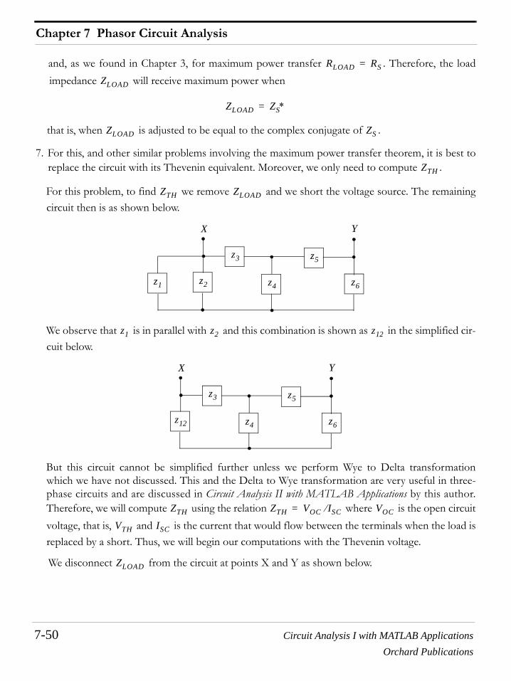
Chapter 7 Phasor Circuit Analysis
7-50 Circuit Analysis I with MATLAB ApplicationsOrchard Publications
and, as we found in Chapter 3, for maximum power transfer . Therefore, the loadimpedance will receive maximum power when
that is, when is adjusted to be equal to the complex conjugate of .
7. For this, and other similar problems involving the maximum power transfer theorem, it is best toreplace the circuit with its Thevenin equivalent. Moreover, we only need to compute .
For this problem, to find we remove and we short the voltage source. The remainingcircuit then is as shown below.
We observe that is in parallel with and this combination is shown as in the simplified cir-cuit below.
But this circuit cannot be simplified further unless we perform Wye to Delta transformationwhich we have not discussed. This and the Delta to Wye transformation are very useful in three-phase circuits and are discussed in Circuit Analysis II with MATLAB Applications by this author.Therefore, we will compute using the relation where is the open circuitvoltage, that is, and is the current that would flow between the terminals when the load isreplaced by a short. Thus, we will begin our computations with the Thevenin voltage.
We disconnect from the circuit at points X and Y as shown below.
RLOAD RS=
ZLOAD
ZLOAD ZS∗=
ZLOAD ZS
ZTH
ZTH ZLOAD
z1
X Y
z2
z3
z4
z5
z6
z1 z2 z12
X Y
z12
z3
z4
z5
z6
ZTH ZTH VOC ISC⁄= VOC
VTH ISC
ZLOAD

Circuit Analysis I with MATLAB Applications 7-51Orchard Publications
Answers to Exercises
We will replace the remaining circuit with its Thevenin equivalent. Thus, with discon-nected the circuit simplifies to that shown below.
Now, we will find
At Node 1:
At Node 2:
and with MATLAB
Vs=170; z1=4; z2=20; z3=10; z4=5j; z5=5−10j;...
4 Ω10 Ω 5 Ω
20 Ω
+
− j5
−j10170 0°∠
ZLDX Y
ZLOAD
4 Ω 5 Ω
20 Ω+
−170 0°∠
X Y10 Ω
j5 Ω
j– 10 Ω
1 2V1 V2 VYz1
z2
z3
z4
z5VS
VTH VXY VX VY– V1 V2 VR5 Ω–( )–= = =
V1 VS–
z1------------------
V1z2------
V1 V2–
z3------------------+ + 0=
1z1---- 1
z2---- 1
z3----+ +⎝ ⎠
⎛ ⎞ V11z3----V2–
VSz1------=
V2 V1–
z3------------------
V2z4------
V2z5------+ + 0=
1z3----V1– 1
z3---- 1
z4---- 1
z5----+ +⎝ ⎠
⎛ ⎞ V2+

Chapter 7 Phasor Circuit Analysis
7-52 Circuit Analysis I with MATLAB ApplicationsOrchard Publications
Y=[1/z1+1/z2+1/z3 −1/z3; −1/z3 1/z3+1/z4+1/z5]; I=[Vs/z1 0]'; V=Y\I; V1=V(1); V2=V(2);... VX=V1; VY=(5/z5)*V2; VTH=VX−VY; fprintf(' \n');...disp('V1 = '); disp(V1); disp('V2 = '); disp(V2);...disp('VTH = '); disp(VTH); fprintf('magVTH = %4.2f V ',abs(VTH));...fprintf('phaseVTH = %4.2f deg ',angle(VTH)*180/pi); fprintf(' \n'); fprintf(' \n');
V1 = 1.1731e+002 + 1.1538e+001i
V2 = 44.2308+46.1538i
VTH = 1.2692e+002 - 1.5385e+001i
magVTH = 127.85 V phaseVTH = -6.91 deg
Thus,
Next, we must find from the circuit shown below.
We will write four mesh equations as shown above but we only are interested in phasor current .Observing that a and b are the same point the mesh equations are
and in matrix form
VTH 127.85 6.91°–∠=
ISC
4 Ω10 Ω 5 Ω
20 Ω
+
− j5
−j10170 0°∠
X Y
VS
ISCz1
z2
z3
z4
z5
z6I1
I2 I3
I4
b
a
I4
z1 z2+( ) I1 z2 I2– VS=
z2 I1– z2 z3 z4+ +( ) I2 z4 I3– z3 I4–+ 0=
z4 I2– z4 z5 z6+ +( ) I3 z5 I4–+ 0=
z3 I2– z5 I3– z3 z5+( ) I4+ 0=
z1 z2+ z2– 0 0z2– z2 z3 z4+ + z4– z3–
0 z4– z4 z5 z6+ + z5–
z3– z5– z3 z5+
I1
I2
I3
I4
⋅
VS
000
=

Circuit Analysis I with MATLAB Applications 7-53Orchard Publications
Answers to Exercises
With MATLAB
Vs=170; VTH=126.92−15.39j; z1=4; z2=20; z3=10; z4=5j; z5=5; z6=−10j;... Z=[z1+z2 −z2 0 0; −z2 z2+z3+z4 −z4 −z3; 0 −z4 z4+z5+z6 −z5; 0 −z3 −z5 z3+z5];...V=[Vs 0 0 0]'; I=Z\V; I1=I(1); I2=I(2); I3=I(3); I4=I(4);... ZTH=VTH/I4; fprintf(' \n'); disp('I1 = '); disp(I1); disp('I2 = '); disp(I2);...disp('I3 = '); disp(I3); disp('I4 ='); disp(I4); disp('ZTH ='); disp(ZTH); fprintf(' \n');
I1 = 15.6745 - 2.6300i
I2 = 10.3094 - 3.1559i
I3 = -1.0520 + 10.7302i
I4 = 6.5223 + 1.4728i
ZTH = 18.0084 - 6.4260i
Thus, and by Problem 6, for maximum power transfer there must be
or
8. We assign phasor currents as shown below.
We choose as a reference, that is, we let
Then,
and since
Next,
and
ZTH 18.09 j6.43 Ω–=
ZLOAD Z∗TH=
ZLOAD 18.09 j6.43 Ω+=
4 Ω 10 Ω 5 Ω
20 Ω
+
−j5
−j10
VS I4
I20
I10
IL
IC
I5
I5
I5 1 0° A∠=
V5 5 0° V∠=
IC I5=
VC IC j10–( )⁄ 1 0°∠ 10 90°–∠⋅ 10 90°– V∠= = =
VL V5 VC+ 5 0° 10 90°–∠+∠ 5 j10–( )+ 5 j10– 11.18 63.4° V–∠= = = = =

Chapter 7 Phasor Circuit Analysis
7-54 Circuit Analysis I with MATLAB ApplicationsOrchard Publications
Now
and
Continuing we find
and
Also,
and
Finally,
The magnitudes (not to scale) and the phase angles are shown below.
The phasor diagram above is acceptable. However, it would be more practical if we rotate it by to show the voltage source as reference at as shown below.
IL VL j5⁄ 11.18 63.4°–∠( ) 5 90°∠( )⁄ 2.24 153.4°–∠ 2– j A–= = = =
I10 IL I5+ 2– j– 1+ 1– j– 2 135° A–∠= = = =
V10 10 2 135°–∠× 10 1– j–( )× 10– j10 V–= = =
V20 V10 VL+ 10– j10– 5 j10–+ 5– j20 V–= = =
I20 V20 20⁄ 5– j20–( ) 20⁄ 0.25– j A–= = =
I4 I20 I10+ 0.25– j– 1– j– 1.25– j2 A–= = =
V4 4I4 4 1.25– j2–( )× 5– j8 V–= = =
VS V4 V20+ 5– j8 5– j20–– 10– j28– 29.73 109.7° V–∠= = = =
IL
VL
I5 IC=
VCVS
V10
V20
V4
I10I4I20
109.7° VS 0°
VS
V20
VC
VLI5 IC=
V4
V10IL
I4I10
I20

Circuit Analysis I with MATLAB Applications 7-55Orchard Publications
Answers to Exercises
9. The equivalent phasor circuit is shown below where , , and
Application of KCL yields
and since the above relation reduces to
or
and with MATLAB
Vin=3; z1=1000; z2=3000; z3=−4000j; Vout=−Vin/(z1/z2+z1/z3);...fprintf(' \n'); disp('Vout = '); disp(Vout); fprintf('magVout = %5.2f V \t',abs(Vout));...fprintf('phaseVout = %5.2f deg \t',angle(Vout)*180/pi); fprintf(' \n'); fprintf(' \n');
Vout = -5.7600 + 4.3200i
magVout = 7.20 V phaseVout = 143.13 deg
Thus,
and
z1 R1 1 KΩ= = z2 R2 3 KΩ= =
z3 j– ωC⁄ j– 10 3 0.25 10 6–××( )⁄ j4 KΩ–= = =
VIN 3 0° V∠=
1 KΩ3 KΩ
z1
z3
z2
VOUT
V
V VIN–
z1------------------
V VOUT–
z2-----------------------
V VOUT–
z3-----------------------+ + 0=
V 0=
1z2---- 1
z3----+⎝ ⎠
⎛ ⎞ VOUTVIN–
z1------------=
VOUTVIN–
z11z2---- 1
z3----+⎝ ⎠
⎛ ⎞⋅----------------------------------
VIN–
z1z2----
z1z3----+⎝ ⎠
⎛ ⎞-------------------------= =
VOUT 5.76– j4.32+ 7.2 143.13° V∠= =
vout t( ) 7.2 1000t 143.13°+( ) Vcos=

Chapter 7 Phasor Circuit Analysis
7-56 Circuit Analysis I with MATLAB ApplicationsOrchard Publications
NOTES

Circuit Analysis I with MATLAB Applications 8-1Orchard Publications
Chapter 8
Average and RMS Values, Complex Power, and Instruments
his chapter defines average and effective values of voltages and currents, instantaneous andaverage power, power factor, the power triangle, and complex power. It also discusses electri-cal instruments that are used to measure current, voltage, resistance, power, and energy.
8.1 Periodic Time Functions
A periodic time function satisfies the expression
(8.1)
where is a positive integer and is the period of the periodic time function. The sinusoidal andsawtooth waveforms of Figure 8.1 are examples of periodic functions of time.
Figure 8.1. Examples of periodic functions of time
Other periodic functions of interest are the square and the triangular waveforms.
T
f t( ) f t nT+( )=
n T
T T
cosωt
T T
cos(ωt+θ)
θ
T T T T
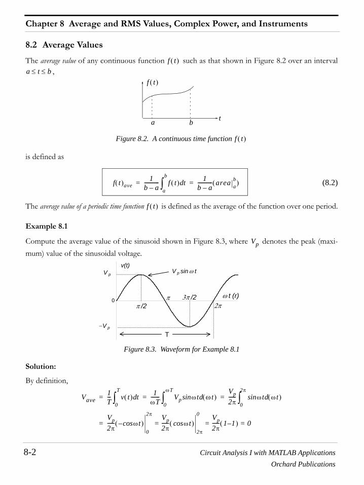
Chapter 8 Average and RMS Values, Complex Power, and Instruments
8-2 Circuit Analysis I with MATLAB ApplicationsOrchard Publications
8.2 Average Values
The average value of any continuous function such as that shown in Figure 8.2 over an interval,
Figure 8.2. A continuous time function
is defined as
(8.2)
The average value of a periodic time function is defined as the average of the function over one period.
Example 8.1
Compute the average value of the sinusoid shown in Figure 8.3, where denotes the peak (maxi-mum) value of the sinusoidal voltage.
Figure 8.3. Waveform for Example 8.1
Solution:
By definition,
f t( )a t b≤ ≤
a bt
f t( )
f t( )
f t( )ave1
b a–------------ f t( ) td
a
b
∫1
b a–------------ area a
b( )= =
f t( )
Vp
0
V p
π /2π 3π /2
2π
−V p
V p sin ω t
ω t (r)
v(t)
T
Vave1T--- v t( ) td
0
T
∫1
ωT------- Vp ωt ωt( )dsin
0
ωT
∫Vp2π------ ωt ωt( )dsin
0
2π
∫= = =
Vp2π------ ωtcos–( )
0
2π Vp2π------ ωtcos( )
2π
0 Vp2π------ 1 1–( ) 0= = ==

Circuit Analysis I with MATLAB Applications 8-3Orchard Publications
Effective Values
as expected since the net area of the positive and negative half cycles is zero.
Example 8.2
Compute the average value of the half-wave rectification waveform shown in Figure 8.4.
Figure 8.4. Waveform for Example 8.2
Solution:
This waveform is defined as
(8.3)
Then, its average value is found from
(8.4)
In other words, the average value of the half-wave rectification waveform is equal to its peak valuedivided by .
8.3 Effective Values
The effective current of a periodic current waveform is defined as the current which producesheat in a given resistance R at the same average rate as a direct (constant) current , that is,
(8.5)
Also, in a periodic current waveform , the instantaneous power is
Half-Wave Rectifier Waveform
Radians
Cur
rent
(I) I p sin ω t
T
π 2π
i t( )Ip ωt sin 0 ωt π< <
0 π ωt 2π< <⎩⎨⎧
=
Iave1
2π------ Ip ωtsin ωt( )d
0
2π
∫1
2π------ Ip ωtsin ωt( ) 0 ωt( )d
π
2π
∫+d0
π
∫= =
Ip2π------ ωt 0
πcos–( )Ip2π------ ωt π
0cosIp2π------ 1 1–( )–[ ]
Ipπ----= = ==
π
Ieff i t( )
Idc
Average Power Pave RIeff2 RIdc
2= = =
i t( )

Chapter 8 Average and RMS Values, Complex Power, and Instruments
8-4 Circuit Analysis I with MATLAB ApplicationsOrchard Publications
(8.6)
and
(8.7)
Equating (8.5) with (8.7) we get
or
or
(8.8)
Caution 1: In general, since the expression implies that the function imust first be squared and the average of the squared value is then to be found. On theother hand, implies that the average value of the function must first be foundand then the average must be squared. The waveform of Figure 8.5 illustrates this point.
Figure 8.5. Waveforms to illustrate that
Caution 2: In general, . For example, if and, then , and also . Thus, . However,
p t( ) R i2 t( )=
Pave1T--- p t( ) td
0
T
∫ 1T--- Ri2 td
0
T
∫ RT--- i2 td
0
T
∫= = =
RIeff2 R
T--- i2 td
0
T
∫=
Ieff2 1
T--- i 2 td
0
T
∫=
Ieff1T--- i 2 td
0
T
∫ IRoot Mean Square IRMS Ave i2( )= = = =
ave i2( ) iave( )2≠ ave i2( )
iave( )2
i 2
i
ave(i2) ≠ 0
0
sqrt(ave(i2)) ≠ 0
iave = 0, i2ave = 0 and sqrt(i2ave) = 0
ave i2( ) iave( )2≠
Pave Vave Iave×≠ v t( ) Vp ωtcos=
i t( ) Ip ωt ϕ+( )cos= Vave 0= Iave 0= Pave 0=
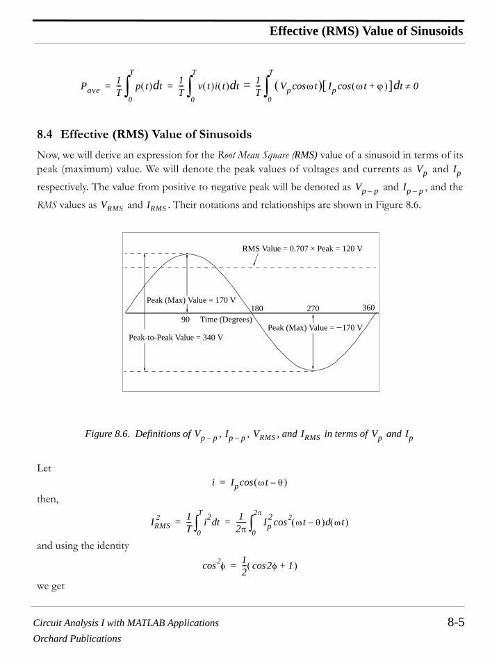
Circuit Analysis I with MATLAB Applications 8-5Orchard Publications
Effective (RMS) Value of Sinusoids
8.4 Effective (RMS) Value of Sinusoids
Now, we will derive an expression for the Root Mean Square (RMS) value of a sinusoid in terms of itspeak (maximum) value. We will denote the peak values of voltages and currents as and respectively. The value from positive to negative peak will be denoted as and , and theRMS values as and . Their notations and relationships are shown in Figure 8.6.
Figure 8.6. Definitions of , , , and in terms of and
Let
then,
and using the identity
we get
Pave1T--- p t( ) td
0
T
∫ 1T--- v t( )i t( ) td
0
T
∫ 1T--- Vp ωtcos( ) Ip ωt ϕ+( )cos[ ] td
0
T
∫= 0≠= =
Vp Ip
Vp p– Ip p–
VRMS IRMS
Peak (Max) Value = 170 V
Peak (Max) Value = −170 V90
180 270 360Time (Degrees)
Peak-to-Peak Value = 340 V
RMS Value = 0.707 × Peak = 120 V
Vp p– Ip p– VRMS IRMS Vp Ip
i Ip ωt θ–( )cos=
IRMS2 1
T--- i2 td
0
T
∫1
2π------ Ip
2ωt θ–( )2cos ωt( )d
0
2π
∫= =
φ2cos 12--- 2φ 1+cos( )=

Chapter 8 Average and RMS Values, Complex Power, and Instruments
8-6 Circuit Analysis I with MATLAB ApplicationsOrchard Publications
(8.9)
Using the trigonometric identities
and
by substitution into (8.9), we get
and therefore,
(8.10)
We observe that the value of a sinusoid is independent of the frequency and phase angle, inother words, it is dependent on the amplitude of the sinusoid only.
Example 8.3
Compute the and for the sawtooth waveform shown in Figure 8.7.
Figure 8.7. Waveform for Example 8.3
Solution:
By inspection, the period is as shown in Figure 8.8.
IRMS2 Ip
2
4π------ 2ωt θ–( )cos ωt( )d ωt( )d
0
2π
∫+0
2π
∫=
Ip2
4π------ 2ωt θ–( )sin
2------------------------------
0
2πωt 0
2π( )+Ip
2
4π------ 4π θ–( ) θ–( )sin–sin
2---------------------------------------------------- 2π+==
x y–( )sin x y x ysincos–cossin=
α–( )sin– αsin=
IRMS2 Ip
2
4π------ 4π θcos 4πcos θ θsin+sin–sin
2---------------------------------------------------------------------------- 2π+
Ip2
4π------ 2π( )
Ip2
2-----= = =
0 1
IRMSIp
2------- 0.707Ip = =
FOR SINUSOIDS ONLY
RMS
Iave IRMS
10 A
t
i t( )
T

Circuit Analysis I with MATLAB Applications 8-7Orchard Publications
RMS Values of Sinusoids with Different Frequencies
Figure 8.8. Defining the period for the waveform of Example 8.3
The average value is
To find we cannot use (8.10); this is for sinusoids only. Accordingly, we must use the definitionof the value as derived in (8.8). Then,
or
8.5 RMS Values of Sinusoids with Different Frequencies
The value of a waveform which consists of a sum of sinusoids of different frequencies, isequal to the square root of the sum of the squares of the values of each sinusoid. Thus, if
(8.11)
where represents a constant current, and represent the amplitudes of the sinusoids.Then, the value of i is found from
(8.12)
or
(8.13)
T
10 A
t
i t( )
IaveArea
Period------------------ 1 2⁄( ) 10 T××
T------------------------------------ 5 A= = =
IRMS
RMS
IRMS2 1
T--- i2 t( ) td
0
T
∫1T--- 10
T------t⎝ ⎠
⎛ ⎞ 2td
0
T
∫1T--- 100
T2--------- t 3
3----⋅
⎝ ⎠⎜ ⎟⎛ ⎞
0
T1T--- 100
T2--------- T 3
3------⋅
⎝ ⎠⎜ ⎟⎛ ⎞ 100
3---------= = = = =
IRMS1003
--------- 103
------- 5.77 A= = =
RMSRMS
i I0 I1 ω1t θ1±( )cos I2 ω2t θ2±( )cos … IN ωN t θN±( )cos+ + + +=
I0 I1 I2… IN, ,
RMS
IRMS I0 2 I1 RMS
2 I2 RMS2 … IN RMS
2+ + + +=
IRMS I0 2 1
2---I
1 p
2 12---I
2 p
2… 1
2---I
N p
2+ + + +=

Chapter 8 Average and RMS Values, Complex Power, and Instruments
8-8 Circuit Analysis I with MATLAB ApplicationsOrchard Publications
Example 8.4
Find the value of the square waveform of Figure 8.9 by application of (8.12)
Figure 8.9. Waveform for Example 8.4
Solution:
By inspection, the period is as shown in Figure 8.9.
Figure 8.10. Determination of the period to the waveform of Example 8.4
Then,a.
or
(8.14)
b. Fourier series analysis textbooks* show that the square waveform above can be expressed as
(8.15)
* Such a textbook is Signals and Systems with MATLAB Applications, ISBN 0-9709511-3-2 by this author.
IRMS
1
−1
ωt
T 2π=
1
−1
ωtπ 2π
IRMS2 1
T--- i 2 td
0
T
∫1
2π------ i 2
ωt( )d0
2π
∫1
2π------ 1 2
ωt( )d0
π
∫ 1–( ) 2ωt( )d
π
2π
∫+= = =
12π------ ωt 0
πωt π
2π+[ ] 12π------ π 2π π–+[ ] 1= ==
IRMS 1=
i t( ) 4π--- ωtsin 1
3--- 3ωtsin 1
5--- 5ωtsin …+ + +⎝ ⎠
⎛ ⎞=

Circuit Analysis I with MATLAB Applications 8-9Orchard Publications
Average Power and Power Factor
and as we know, the value of a sinusoid is a real number independent of the frequencyand the phase angle, and it is equal to times its peak value, that is, .Then from (8.12) and (8.15),
(8.16)
The numerical accuracy of (8.16) is good considering that higher harmonics have beenneglected.
8.6 Average Power and Power Factor
Consider the network shown in Figure 8.11.
Figure 8.11. Network where it is assumed that and are out-of-phase
We will assume that the load current is degrees out-of-phase with the voltage ,i.e., if , then . We want to find an expression for theaverage power absorbed by the load.
As we know
that is,
and the instantaneous power absorbed by the load is
(8.17)
Using the trigonometric identity
we express (8.17) as
RMS0.707 IRMS 0.707 Ip×=
IRMS4π--- 0 1
2--- 1( )2 1
2--- 1
3---⎝ ⎠
⎛ ⎞ 2 12--- 1
5---⎝ ⎠
⎛ ⎞ 2…+ + + + 0.97= =
R +
−
Rest ofthe Circuit Load
vS t( )
iLOAD t( )
vLOAD t( )
iLOAD t( ) vLOAD t( )
iLOAD t( ) θ vLOAD t( )
vLOAD t( ) Vp ωtcos= iLOAD t( ) Ip ωt θ+( )cos=
p vi=
ins eous powertantan ins eous voltage ins eous currenttantan×tantan=
pLOAD t( )
pLOAD t( ) vLOAD t( ) iLOAD t( )× VpIp ωtcos ωt θ+( )cos×= =
x ycoscos 12--- x y+( ) x y–( )cos+cos[ ]=

Chapter 8 Average and RMS Values, Complex Power, and Instruments
8-10 Circuit Analysis I with MATLAB ApplicationsOrchard Publications
(8.18)
and the average power is
(8.19)
We observe that the first integral on the right side of (8.19) is zero, and the second integral, being aconstant, has an average value of that constant. Then,
(8.20)
and using the relations
and
we can express (8.19) as
(8.21)
and it is imperative that we remember that these relations are valid for circuits with sinusoidal excitations.
The term in (8.20) and (8.21) is known as the power factor and thus
(8.22)
8.7 Average Power in a Resistive Load
The voltage and current in a resistive branch of a circuit are always in phase, that is, the phase angle. Therefore, denoting that resistive branch with the subscript we have:
pLOAD t( )VpIp
2----------- 2ωt θ+( ) θcos+cos[ ]=
Pave LOAD1T--- pLD td
0
T
∫1T---
VpIp2
----------- 2ωt θ+( ) θcos+cos[ ]⎝ ⎠⎛ ⎞ td
0
T
∫= =
VpIp2T
----------- 2ωt θ+( )cos[ ]( ) td0
T
∫VpIp2T
----------- θcos td0
T
∫+=
Pave LOAD
VpIp2
---------- θcos=
VRMSVp
2-------=
IRMSIp
2-------=
Pave LOADVRMS LOAD IRMS LOAD θcos=
θcos
Power FactorLOAD PFLOAD θLOADcosPave LOAD
VRMS LOAD IRMS LOAD------------------------------------------------------= = =
θ 0°= R

Circuit Analysis I with MATLAB Applications 8-11Orchard Publications
Average Power in Inductive and Capacitive Loads
(8.23)
or
(8.24)
8.8 Average Power in Inductive and Capacitive Loads
With inductors and capacitors there is a phase difference between the voltage and current, that
is, and therefore, denoting that inductive or capacitive branch with the subscript we get:
Of course, the instantaneous power is zero only at specific instants.
Obviously, if the load of a circuit contains resistors, inductors and capacitors, the phase angle between and will be within , and the power factor will bewithin .
Example 8.5
For the circuit of Figure 8.11, find the average power supplied by the voltage source, the averagepower absorbed by the resistor, the inductor, and the capacitor.
Figure 8.12. Circuit for Example 8.5
Solution:
Since this is a series circuit, we need to find the current I and its phase relation to the source voltage. Then,
(8.25)
Pave R VRMS R IRMS R 0° VRMS R IRMS R=cos=
Pave RVRMS R
2
R----------------- IRMS R
2 R 12---
Vm R2
R----------- 1
2---Ip R
2 R= = = =
90°
θ 90°= X
Pave X VRMS X IRMS X 90° 0=cos=
θ
VRMS LOAD IRMS LOAD 0 θ 90°≤ ≤ θcos
0 θcos 1≤ ≤
I
VS 170 0°∠= j– 10 Ω
10 Ω j20 Ω
VS
IVSZ------ 170 0°∠
10 j20 j10–+---------------------------------- 170 0°∠
10 j10+-------------------- 170 0°∠
10 2 45°∠--------------------------- 12 45°–∠= = = = =
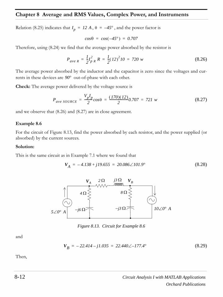
Chapter 8 Average and RMS Values, Complex Power, and Instruments
8-12 Circuit Analysis I with MATLAB ApplicationsOrchard Publications
Relation (8.25) indicates that , , and the power factor is
Therefore, using (8.24) we find that the average power absorbed by the resistor is
(8.26)
The average power absorbed by the inductor and the capacitor is zero since the voltages and cur-rents in these devices are out-of-phase with each other.
Check: The average power delivered by the voltage source is
(8.27)
and we observe that (8.26) and (8.27) are in close agreement.
Example 8.6
For the circuit of Figure 8.13, find the power absorbed by each resistor, and the power supplied (orabsorbed) by the current sources.
Solution:
This is the same circuit as in Example 7.1 where we found that
(8.28)
Figure 8.13. Circuit for Example 8.6
and
(8.29)
Then,
Ip 12 A= θ 45°–=
θcos 45°–( )cos 0.707= =
Pave R12---Ip R
2 R 12--- 12( )210 720 w= = =
90°
Pave SOURCE
VpIp2
----------- θcos 170( ) 12( )2
-------------------------0.707 721 w= = =
VA 4.138– j19.655+ 20.086 101.9°∠= =
8 Ω
2 Ω
4 Ω
j3 Ω
−j6 Ω −j3 Ω5 0° A∠
10 0° A∠
VBVA
VB 22.414– j1.035– 22.440 177.4– °∠= =
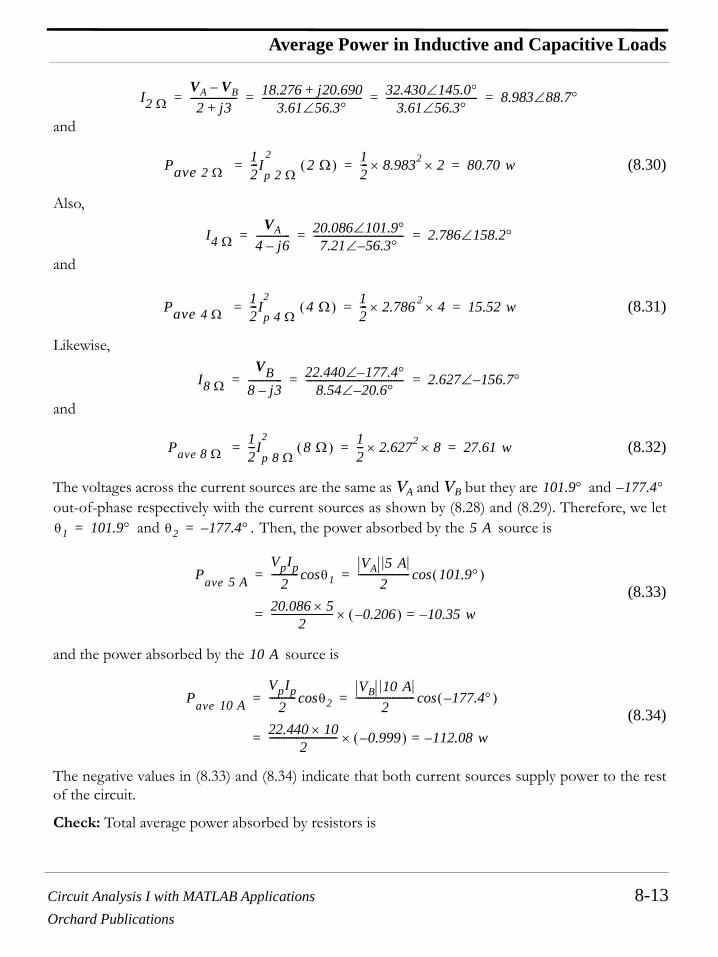
Circuit Analysis I with MATLAB Applications 8-13Orchard Publications
Average Power in Inductive and Capacitive Loads
and
(8.30)
Also,
and
(8.31)
Likewise,
and
(8.32)
The voltages across the current sources are the same as VA and VB but they are and out-of-phase respectively with the current sources as shown by (8.28) and (8.29). Therefore, we let
and . Then, the power absorbed by the source is
(8.33)
and the power absorbed by the source is
(8.34)
The negative values in (8.33) and (8.34) indicate that both current sources supply power to the restof the circuit.
Check: Total average power absorbed by resistors is
I2 ΩVA VB–
2 j3+------------------- 18.276 j20.690+
3.61 56.3°∠----------------------------------------- 32.430 145.0°∠
3.61 56.3°∠------------------------------------- 8.983 88.7°∠= = = =
Pave 2 Ω 12---I
p 2 Ω 2
2 Ω( ) 12--- 8.9832× 2× 80.70 w= = =
I4 ΩVA
4 j6–-------------- 20.086 101.9°∠
7.21 56.3°–∠------------------------------------- 2.786 158.2°∠= = =
Pave 4 Ω 12---I
p 4 Ω 2
4 Ω( ) 12--- 2.786 2× 4× 15.52 w= = =
I8 ΩVB
8 j3–-------------- 22.440 177.4– °∠
8.54 20.6°–∠---------------------------------------- 2.627 156.7– °∠= = =
Pave 8 Ω 12---I
p 8 Ω
28 Ω( ) 1
2--- 2.6272× 8× 27.61 w= = =
101.9° 177.4°–
θ1 101.9°= θ2 177.4– °= 5 A
Pave 5 AVpIp
2----------- θcos 1
VA 5 A2
--------------------- 101.9°( )cos= =
20.086 5×2
------------------------- 0.206–( )× 10.35 w–==
10 A
Pave 10 AVpIp
2----------- θcos 2
VB 10 A2
------------------------ 177.4– °( )cos= =
22.440 10×2
---------------------------- 0.999–( )× 112.08 w–==

Chapter 8 Average and RMS Values, Complex Power, and Instruments
8-14 Circuit Analysis I with MATLAB ApplicationsOrchard Publications
and the total average power supplied by current sources is
Thus, the total average power supplied by the current sources is equal to the total average powerabsorbed by the resistors. The small difference is due to rounding of fractional numbers.
8.9 Average Power in Non-Sinusoidal Waveforms
If the excitation in a circuit is non-sinusoidal, we can compute the average power absorbed by aresistor from the relations
(8.35)
Example 8.7
Compute the average power absorbed by a resistor when the voltage across it is the half-waverectification waveform shown in Figure 8.14.
Figure 8.14. Waveform for Example 8.7
Solution:
We first need to find the numerical value of . It is found as follows:
and thus
Then,
80.70 15.52 27.61+ + 123.83 w=
112.08 10.35+ 122.43 w=
Pave1T--- p td
0
T
∫1T--- v 2
R------ td
0
T
∫1T--- i2R td
0
T
∫= = =
5 Ω
Half-Wave Rectifier Waveform
t (ms)
Vol
tage
(V)
10sinωt
1 2
ω
T 2 ms 2 10 3–× s ωT 2π ω2πT
------ 103π= = = = =
10 ωtsin 10 103πsin=
Pave1T--- v 2
R------ td
0
T
∫1
2 10 3–×-------------------- 10 2 10 3
πt2sin5
----------------------------------0
10 3–
∫ 010 3–
2 10 3–×
∫+ dt= =
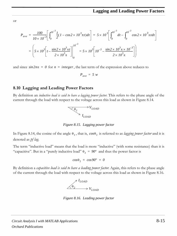
Circuit Analysis I with MATLAB Applications 8-15Orchard Publications
Lagging and Leading Power Factors
or
and since for , the last term of the expression above reduces to
8.10 Lagging and Leading Power Factors
By definition an inductive load is said to have a lagging power factor. This refers to the phase angle of thecurrent through the load with respect to the voltage across this load as shown in Figure 8.14.
Figure 8.15. Lagging power factor
In Figure 8.14, the cosine of the angle , that is, is referred to as lagging power factor and it isdenoted as pf lag.
The term “inductive load” means that the load is more “inductive” (with some resistance) than it is“capacitive”. But in a “purely inductive load” and thus the power factor is
By definition a capacitive load is said to have a leading power factor. Again, this refers to the phase angleof the current through the load with respect to the voltage across this load as shown in Figure 8.16.
Figure 8.16. Leading power factor
Pave100
10 10 3–×----------------------- 1
2--- 1 2 10 3πt×cos–( )dt
0
10 3–
∫ 5 10 3 dt0
10 3–
∫ 2 10 3πt×cos dt
0
10 3–
∫–×= =
5 103 t 2 103πt×sin
2 103π×
-------------------------------–
0
10 3–
× 5 103 10 3– 2 103π 10 3–××sin
2 103π×
----------------------------------------------–×=⎝ ⎠⎜ ⎟⎜ ⎟⎛ ⎞
=
2nπsin 0= n integer=
Pave 5 w=
VLOAD
ILOAD
θ1
θ1 θ1cos
θ1 90°=
θ1cos 90°cos 0= =
VLOAD
ILOAD
θ2
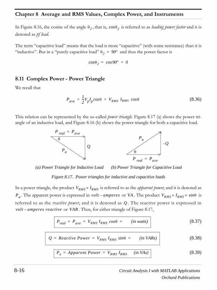
Chapter 8 Average and RMS Values, Complex Power, and Instruments
8-16 Circuit Analysis I with MATLAB ApplicationsOrchard Publications
In Figure 8.16, the cosine of the angle , that is, is referred to as leading power factor and it isdenoted as pf lead.
The term “capacitive load” means that the load is more “capacitive” (with some resistance) than it is“inductive”. But in a “purely capacitive load” and thus the power factor is
8.11 Complex Power - Power Triangle
We recall that
(8.36)
This relation can be represented by the so-called power triangle. Figure 8.17 (a) shows the power tri-angle of an inductive load, and Figure 8.16 (b) shows the power triangle for both a capacitive load.
Figure 8.17. Power triangles for inductive and capacitive loads
In a power triangle, the product is referred to as the apparent power, and it is denoted as. The apparent power is expressed in or . The product is
referred to as the reactive power, and it is denoted as . The reactive power is expressed in or . Thus, for either triangle of Figure 8.17,
(8.37)
(8.38)
(8.39)
θ2 θ2cos
θ2 90°=
θ2cos 90°cos 0= =
Pave12---VpIp θcos VRMS IRMS θcos= =
(a) Power Triangle for Inductive Load (b) Power Triangle for Capacitive Load
Q−Q
P real Pave=
P real Pave=
θ
θ Pa
Pa
VRMS IRMS×
Pa volt amperes– VA VRMS IRMS× θsin×
Qvolt amperes reactive– VAR
Preal Pave VRMS IRMS θcos (in watts)= = =
Q Reactive Power VRMS IRMS θsin (in VARs)= = =
Pa Apparent Power VRMS IRMS (in VAs)= =
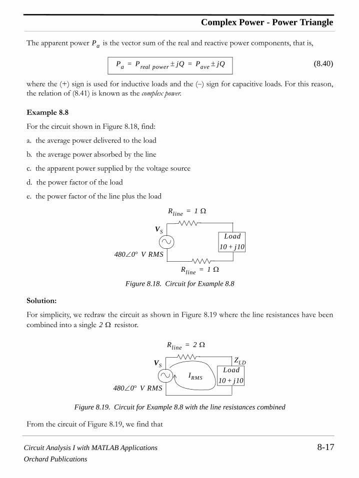
Circuit Analysis I with MATLAB Applications 8-17Orchard Publications
Complex Power - Power Triangle
The apparent power is the vector sum of the real and reactive power components, that is,
(8.40)
where the (+) sign is used for inductive loads and the (−) sign for capacitive loads. For this reason,the relation of (8.41) is known as the complex power.
Example 8.8
For the circuit shown in Figure 8.18, find:
a. the average power delivered to the load
b. the average power absorbed by the line
c. the apparent power supplied by the voltage source
d. the power factor of the load
e. the power factor of the line plus the load
Figure 8.18. Circuit for Example 8.8
Solution:
For simplicity, we redraw the circuit as shown in Figure 8.19 where the line resistances have beencombined into a single resistor.
Figure 8.19. Circuit for Example 8.8 with the line resistances combined
From the circuit of Figure 8.19, we find that
Pa
Pa P powerreal jQ± Pave jQ±= =
Rline 1 Ω=
Rline 1 Ω=
VS
480 0° V RMS∠
Load10 j10+
2 Ω
Rline 2 Ω=
VS
480 0° V RMS∠
Load10 j10+
IRMS
ZLD

Chapter 8 Average and RMS Values, Complex Power, and Instruments
8-18 Circuit Analysis I with MATLAB ApplicationsOrchard Publications
and therefore, the current lags the voltage as shown on the phasor diagram of Figure 8.20.
Figure 8.20. Phasor diagram for the circuit of Example 8.8
Then,
a. The average power delivered to the load is
b. The average power absorbed by the line is
c. The apparent power supplied by the voltage source is
d. The power factor of the load is
e. The power factor of the line plus the load is
8.12 Power Factor Correction
The consumer pays the electric utility company for the average or real power, not the apparentpower and, as we have seen, a low power factor (larger angle ) demands more current. This addi-tional current must be furnished by the utility company which must provide larger current-carryingcapacity if the voltage must remain constant. Moreover, this additional current creates larger
IRMSVS RMS
Rline ZLD+---------------------------- 480 0°∠
2 10 j10+ +----------------------------- 480 0°∠
15.62 39.8°∠------------------------------- 30.73 39.8°–∠= = = =
I
VS39.8°–
Pave LOAD IRMS2 Re ZLOAD 30.73( )2 10× 9443 w 9.443 Kw= = = =
Pave line IRMS2 Rline 30.73( )2 2× 1889 w 1.889 Kw= = = =
Pa source VS RMS IRMS 480 30.73× 14750 w 14.750 Kw= = = =
pfLOAD θLOADcosPave LOADPa LOAD
------------------------ 9443VRMS LOAD IRMS--------------------------------------------= = =
9443480 0°∠ 2 30.73 39.8°–∠( )–( ) 30.73×
------------------------------------------------------------------------------------------------ 9443434.56( ) 30.73( )
---------------------------------------- 944313354--------------- 0.707= = ==
pf line LOAD+( ) θcos line LOAD+( )
Pave totalPa source----------------------
Pave line Pave LOAD+
Pa source----------------------------------------------------- 1889 9443+
14750------------------------------ 0.77= = = = =
θ
i2R

Circuit Analysis I with MATLAB Applications 8-19Orchard Publications
Power Factor Correction
losses in the utility’s transmission and distribution system. For this reason, electric utility companiesimpose a penalty on industrial facility customers who operate at a low power factor, typically lowerthan . Accordingly, facility engineers must install the appropriate equipment to raise the powerfactor.
The power factor correction procedure is illustrated with the following example.
Example 8.9
In the circuit shown in Figure 8.21, the resistance of the lines between the voltage source and theload and the internal resistance of the source are considered small, and thus can be neglected.
Figure 8.21. Circuit for Example 8.9
It is desired to “raise” the power factor of the load to 0.95 lagging. Compute the size and the ratingof a capacitor which, when added across the load, will accomplish this.
Solution:
The power triangles for the existing and desired power factors are shown in Figure 8.22.
Figure 8.22. Power triangles for existing and desired power factors
Since the voltage across the given load must not change (otherwise it will affect the operation of it),it is evident that a load, say , in opposite direction of must be added, and must be connectedin parallel with the existing load. Obviously, the load must be capacitive. Accordingly, the circuitof Figure 8.21 must be modified as shown in Figure 8.23.
0.85
1 Kw Load@ pf =0.8 lag
480 0° V RMS∠
VS
60 Hz
1 Kw 1 Kw
This is what we have This is what we want
θ1θ2
θ1 0.81–cos 36.9°= = θ2 0.951–cos 18.2°= =
Q2Q1
Q3 Q1
Q3

Chapter 8 Average and RMS Values, Complex Power, and Instruments
8-20 Circuit Analysis I with MATLAB ApplicationsOrchard Publications
Figure 8.23. Circuit for power factor correction
For the existing load,
and for the desired , the VAR value of must be reduced to
Therefore, the added capacitive load must be a vector such that
The current through the capacitive load is found from
Then,
and
Therefore, the capacitive load must consist of a capacitor with the value
However, not any capacitor will do; the capacitor must be capable of withstanding a maxi-mum voltage of
and for all practical purposes, we can choose a capacitor rated at 700 volts or higher.
1 Kw Load@ pf =0.8 lag
CapacitiveLoad withLeading pf
480 0° V RMS∠ 60 Hz
VSIC
Q1 1 Kw( ) 36.9°tan 750 VAR= =
pf θ2cos 0.95= = Q2
Q2 1 Kw( ) 18.2°tan 329 VAR= =
Q3
Q3 Q1 Q2– 750 329– 421 VAR= = =
IC
Q3 ICVC ICVS= =
ICQ3
VS RMS----------------- 421
480--------- 0.88 A= = =
XCVCIC------ 480
0.88---------- 547 Ω= = =
C 1ωXC---------- 1
2πf XC---------------- 1
2π 60( ) 547( )------------------------------- 4.85 µF= = = =
4.85 µF
VC max 2 480× 679 V= =
5 µF

Circuit Analysis I with MATLAB Applications 8-21Orchard Publications
Instruments
8.13 Instruments
Ammeters are electrical instruments used to measure current in electric circuits, voltmeters measurevoltage, ohmmeters measure resistance, wattmeters measure power, and watt-hour meters measure elec-tric energy. Voltmeters, Ohmmeters, and Milliammeters (ammeters which measure current in milli-amperes) are normally combined into one instrument called VOM. Figure 8.24 shows a typical ana-log type VOM, and Figure 8.25 shows a typical digital type VOM. We will see how a digital VOMcan be constructed from an analog VOM equivalent at the end of this section. An oscilloscope is anelectronic instrument that produces an instantaneous trace on the screen of a cathode-ray tube cor-responding to oscillations of voltage and current. A typical oscilloscope is shown in Figure 8.26.
DC ammeters and voltmeters read average values whereas AC ammeters and voltmeters read RMS values.
The basic meter movement consists of a permanent horse shoe magnet, an electromagnet whichtypically is a metal cylinder with very thin wire wound around it which is referred to as the coil, anda control spring. The coil is free to move on pivots, and when there is current in the coil, a torque isproduced that tends to rotate the coil. Rotation of the coil is restrained by a helical spring so that themotion of the coil and the pointer which is attached to it, is proportional to the current in the coil.
Figure 8.24. A typical analog VOM
An ammeter measures current in amperes. For currents less than one ampere, a milliammeter ormicroammeter may be used where the former measures current in milliamperes and the latter inmicroamperes.
Ammeters, milliammeters, and microammeters must always be connected in series with the circuits in whichthey are used.
Often, the electric current to be measured, exceeds the range of the instrument. For example, wecannot directly measure a current of to milliamperes with a milliammeter whose range is to
milliampere. In such a case, we can use a low range milliammeter with a shunt (parallel) resistor as5 10 0
1

Chapter 8 Average and RMS Values, Complex Power, and Instruments
8-22 Circuit Analysis I with MATLAB ApplicationsOrchard Publications
shown in Figure 8.27, where the circle with represents an ideal milliammeter (a milliammeterwith zero resistance). In Figure 8.27 is the total current to be measured, is the current throughthe meter, is the current through the shunt resistor, is the milliammeter internal resistance,and is the shunt resistance.
Figure 8.25. A typical digital VOM
Figure 8.26. A typical oscilloscope
mAIT IM
IS RM
RS

Circuit Analysis I with MATLAB Applications 8-23Orchard Publications
Instruments
Figure 8.27. Milliammeter with shunt resistor
From the circuit of Figure 8.27, we observe that the sum of the current flowing through the mil-liammeter and the current through the shunt resistor is equal to the total current , that is,
(8.41)
Also, the shunt resistor is in parallel with the milliammeter branch; therefore, the voltages acrossthese parallel branches are equal, that is,
and since we normally need to calculate the shunt resistor, then
(8.42)
Example 8.10
In the circuit of Figure 8.28, the total current entering the circuit is and the milliammeterrange is to milliampere, that is, the milliammeter has a full-scale current of , and itsinternal resistance is . Compute the value of the shunt resistor .
Figure 8.28. Circuit for Example 8.10
mAIT IM
IT
RM
RS
IS
RS
IM IS IS
IT IM IS+=
RS
RM IM RS IS=
RSIMIS-----RM=
5 mA0 1 Ifs 1 mA
40 Ω RS
40 ΩmA
IT IMIT
RM
RS
=Maximum allowable current IM through the milliammeter
Ifs 1 mA=
IS
Chapter 8 Average and RMS Values, Complex Power, and Instruments
8-24 Circuit Analysis I with MATLAB ApplicationsOrchard Publications
Solution:
The maximum current that the milliammeter can allow to flow through it is and since the totalcurrent is milliamperes, the remaining milliamperes must flow through the shunt resistor, thatis,
The required value of the shunt resistor is found from (8.42), i.e.,
Check: The calculated value of the shunt resistor is ; this is one-fourth the value of the mil-liammeter internal resistor of . Therefore, the resistor will allow four times asmuch current as the milliammeter to flow through it.
A multi-range ammeter/milliammeter is an instrument with two or more scales. Figure 8.29 shows thecircuit of a typical multi-range ammeter/milliammeter.
Figure 8.29. Circuit for a multi-range ammeter/milliammeter
A voltmeter, as stated earlier, measures voltage in volts. Typically, a voltmeter is a modified milliam-meter where an external resistor is connected in series with the milliammeter as shown in Figure8.30 where
1 mA5 4
IS IT IM– 5 1– 4 mA= = =
RSIMIS-----RM
14--- 40× 10 Ω= = =
10 Ω40 Ω 10 Ω
AIT
IM
IT
RMRS
IS
+
−
RV
I current through circuit=
RM internal resis cetan of milliameter=
RV external resistor in series with RM =
VM voltmeter full scale reading=

Circuit Analysis I with MATLAB Applications 8-25Orchard Publications
Instruments
Figure 8.30. Typical voltmeter circuit
For the circuit of Figure 8.30,
or
(8.43)
Voltmeters must always be connected in parallel with those devices of the circuit whose voltage is to be mea-sured.
Example 8.11
Design a voltmeter which will have a volt full-scale using a milliammeter with milliampere full-scale and internal resistance .
Solution:
The voltmeter circuit consists of the milliammeter circuit and the external resistance as shown inFigure 8.31.
Figure 8.31. Circuit for Example 8.11
Here, we only need to compute the value of the external resistor so that the voltage across theseries combination will be full scale. Then, from (8.43),
mAIM
RM RV
VM
= Voltmeter internal resistanceRV
= Voltmeter rangeVM
−+
IM RM RV+( ) VM=
RVVMIM------- RM–=
1 1100 Ω
RV
mAIM
RM RV
VM−+
100 Ω
RV
1 volt

Chapter 8 Average and RMS Values, Complex Power, and Instruments
8-26 Circuit Analysis I with MATLAB ApplicationsOrchard Publications
(8.44)
Therefore, to convert a 1 milliampere full-scale milliammeter with an internal resistance of toa full-scale voltmeter, we only need to attach a resistor in series with that milliamme-ter.
Figure 8.32 shows a typical multi-range voltmeter.
Figure 8.32. Circuit for a multi-range voltmeter
An Ohmmeter measures resistance in Ohms. In the series type Ohmmeter, the resistor whoseresistance is to be measured, is connected in series with the Ohmmeter circuit shown in Figure 8.33.
Figure 8.33. Circuit for a series type Ohmmeter
We observe from Figure 8.33 that for the series type Ohmmeter, the current is maximum whenthe resistor is zero (short circuit), and the current is zero when is infinite (open circuit). Forthis reason, the (zero) point appears on the right-most point of the Ohmmeter scale, and theinfinity symbol appears on the left-most point of the scale.
Figure 8.34 shows the circuit of a shunt (parallel) type Ohmmeter where the resistor whose valueis to be measured, is in parallel with the Ohmmeter circuit.
RVVMIM------- RM– 1
10 3–---------- 100– 1000 100– 900 Ω= = = =
100 Ω1 volt 900 Ω
mARM
VM+ −
900 Ω
9.9 kΩ
99.9 kΩ
100 Ω
IM = 1 mA fs
100 V
10 V
1 V
I
RX
∞ 0mA
I
RM ZeroAdjust−
+VS
RX
IRX RX
0
RX

Circuit Analysis I with MATLAB Applications 8-27Orchard Publications
Instruments
Figure 8.34. Circuit for a parallel type Ohmmeter
From Figure 8.34 we see that, for the shunt type Ohmmeter, the current through the milliammetercircuit is zero when the resistor is zero (short circuit) since all current flows through that short.However, when is infinite (open circuit), the current through the milliammeter branch is maxi-mum. For this reason, the (zero) point appears on the left-most point of the Ohmmeter scale, andthe infinity symbol appears on the right-most point of the scale.
An instrument which can measure unknown resistance values very accurately is the Wheatstone Bridgeshown in Figure 8.35.
Figure 8.35. Wheatstone Bridge Circuit
One of the resistors, say , is the unknown resistor whose value is to be measured, and anotherresistor, say is adjusted until the bridge is balanced, that is, until there is no current flow throughthe meter of this circuit. This balance occurs when
from which the value of the unknown resistor is found from
(8.45)
mAI
RM
ZeroAdjust−
+VS
RX
∞0
RX
RX
0
+−
0
+−VA VB
R3
R4R2
R1VS µA
µA
R4
R3
R1R2------
R3R4------=
R4R2R1------R3=

Chapter 8 Average and RMS Values, Complex Power, and Instruments
8-28 Circuit Analysis I with MATLAB ApplicationsOrchard Publications
Example 8.12
In the Wheatstone Bridge circuit of Figure 8.36, resistor is adjusted until the meter reads zero,and when this occurs, its value is . Compute the value of the unknown resistor .
Figure 8.36. Circuit for Example 8.12
Solution:
When the bridge is balanced, that is, when the current through the meter is zero, relation (8.45)holds. Then,
When measuring resistance values, the voltage sources in the circuit to which the unknown resistance is con-nected must be turned off, and one end of the resistor whose value is to be measured must be disconnected fromthe circuit.
Because of their great accuracy, Wheatstone Bridges are also used to accept or reject resistors whosevalues exceed a given tolerance.
A wattmeter is an instrument which measures power in watts or kilowatts. It is constructed with twosets of coils, a current coil and a voltage coil where the interacting magnetic fields of these coils pro-duce a torque which is proportional to the product.
A watt-hour meter is an instrument which measures electric energy , where is the product of theaverage power in watts and time in hours, that is, in watt-hours. Electric utility compa-nies use kilowatt-hour meters to bill their customers for the use of electricity.
Digital meters include an additional circuit called analog-to-digital converter (ADC).
There are different types of analog-to-digital converters such as the flash converter, the time-windowconverter, slope converter and tracking converter. We will discuss the flash converter only because of itssimplicity. This and the other types are discussed in digital circuits textbooks.
As shown in Figure 8.37, the flash type ADC consists of a resistive network, comparators (denoted as tri-angles), and an eight-to-three line encoder.
R3
120 Ω R4
600 Ω
200 Ω
+−
0
+−120 Ω
VA VB
R3
R4
R2
R1
VS µA
µA
R4R2R1------R3
200600--------- 120× 40 Ω= = =
V I×
W WP t W Pt=

Circuit Analysis I with MATLAB Applications 8-29Orchard Publications
Instruments
Figure 8.37. Typical analog-to-digital converter
† Underflow‡ Overflow
A digital-to-analog converter (DAC) performs the inverse operation, that is, it converts digital values toequivalent analog values.
Figure 8.38 shows a four-bit R-2R ladder network and an op-amp connected to form a DAC.
Analog Input A8 A7 A6 A5 A4 A3 A2 A1 A0 B2 B1 B0
Less than 0 V 0 0 0 0 0 0 0 0 0 x x x†0 to less than 1.5 V 0 0 0 0 0 0 0 0 1 0 0 01.5 to less than 3.0 V 0 0 0 0 0 0 0 1 1 0 0 13.0 to less than 4.5 V 0 0 0 0 0 0 1 1 1 0 1 04.5 to less than 6.0 V 0 0 0 0 0 1 1 1 1 0 1 16.0 to less than 7.5 V 0 0 0 0 1 1 1 1 1 1 0 07.5 to less than 9.0 V 0 0 0 1 1 1 1 1 1 1 0 19.0 to less than 10.5 V 0 0 1 1 1 1 1 1 1 1 1 010.5 to 12 V 0 1 1 1 1 1 1 1 1 1 1 1Greater than 12 V 1 1 1 1 1 1 1 1 1 x x x‡
ANALOG-TO-DIGITAL CONVERTER12 V Supply
−+
−+
Overflow
−+
−+
−+
−+
−+
−+
−+
Analog Input
12 V
10.5 V
9 V
7.5 V
3 V
4.5 V
6 V
1.5 V
0 V
8-to-3
Encoder
B2
B1
B0
A8
A7
A6
A5
A4
A3
A2
A1
A0
−+
VX
VYAi
Inputs Output
Comparator
VX < VY
VX > VY Ai = 0Ai = 1
For Example, if Analog Input = 5.2 V, then A0 = A1 = A2 = A3 = 1and A4 = A5 = A6 = A7 = A8 = 0
VX = VY Previous Value
Chapter 8 Average and RMS Values, Complex Power, and Instruments
8-30 Circuit Analysis I with MATLAB ApplicationsOrchard Publications
Figure 8.38. A typical digital-to-analog converter
8.14 Summary
• A periodic time function is one which satisfies the relation where n is a positiveinteger and T is the period of the periodic time function.
• The average value of any continuous function over an interval ,is defined as
• The average value of a periodic time function is defined as the average of the function overone period.
• A half-wave rectification waveform is defined as
DIGITAL-TO-ANALOG CONVERTER
Negative reference voltage is used so that the
− 1 Volt
B3B2B1B0
−+
Switch Settings: For Logic “0” (ground) positioned to the right
R R R2R
2R 2R 2R 2R
2R
+
−(lsb) (msb)
For Logic “1” (+5 V) positioned to the left
With the switches positioned as shown, B3 B2 B1 B0 = 0100
inverting op amp’s output will be positive.
Vout
lsb = least significant bitmsb = most significant bit
f t( ) f t nT+( )=
f t( ) a t b≤ ≤
f t( )ave1
b a–------------ f t( ) td
a
b
∫1
b a–------------ area a
b( )= =
f t( )
f t( )A ωt sin 0 ωt π< <
0 π ωt 2π< <⎩⎨⎧
=
Circuit Analysis I with MATLAB Applications 8-31Orchard Publications
Summary
• The effective current of a periodic current waveform is defined as
• For sinusoids only,
• For sinusoids of different frequencies,
• For circuits with sinusoidal excitations the average power delivered to a load is
where is the phase angle between and and it is within the range , and is known as the power factor defined within the range .
• The average power in a resistive load is
• The average power in inductive and capacitive loads is
• If the excitation in a circuit is non-sinusoidal, we can compute the average power absorbed by aresistor from the relations
• An inductive load is said to have a lagging power factor and a capacitive load is said to have aleading power factor.
• In a power triangle
Ieff i t( )
Ieff1T--- i 2 td
0
T
∫ IRoot Mean Square IRMS Ave i2( )= = = =
IRMS Ip 2⁄ 0.707Ip= =
IRMS I0 2 I1 RMS
2 I2 RMS2 … IN RMS
2+ + + +=
Pave LOAD
VpIp2
---------- θcos VRMS LOAD IRMS LOAD θcos= =
θ VLOAD ILOAD 0 θ 90°≤ ≤
θcos 0 θcos 1≤ ≤
Pave RVRMS R
2
R----------------- IRMS R
2 R= =
Pave X VRMS X IRMS X 90° 0=cos=
Pave1T--- p td
0
T
∫1T--- v 2
R------ td
0
T
∫1T--- i2R td
0
T
∫= = =
Preal Pave VRMS IRMS θcos (in watts)= =
Q Reactive Power VRMS IRMS θsin (in VARs)= =
Pa Apparent Power VRMS IRMS (in VAs)= =

Chapter 8 Average and RMS Values, Complex Power, and Instruments
8-32 Circuit Analysis I with MATLAB ApplicationsOrchard Publications
• The apparent power , also known as complex power, is the vector sum of the real and reactivepower components, that is,
where the (+) sign is used for inductive loads and the (−) sign for capacitive loads.
• A power factor can be corrected by placing a capacitive load in parallel with the load of the cir-cuit.
• Ammeters are instruments used to measure current in electric circuits. Ammeters, milliammeters,and microammeters must always be connected in series with the circuits in which they are used.
• Voltmeters are instruments used to measure voltage. Voltmeters must always be connected in par-allel with those devices of the circuit whose voltage is to be measured.
• Ohmmeters are instruments used to measure resistance. When measuring resistance values, thevoltage sources in the circuit to which the unknown resistance is connected must be turned off,and one end of the resistor whose value is to be measured must be disconnected from the circuit.
• A Wheatstone Bridge is an instrument which can measure unknown resistance values very accu-rately.
• Voltmeters, Ohmmeters, and Milliammeters (ammeters which measure current in milliamperes)are normally combined into one instrument called VOM.
• Wattmeters are instruments used to measure power.
• Watt-Hour meters are instruments used to measure energy.
• An oscilloscope is an electronic instrument that produces an instantaneous trace on the screen ofa cathode-ray tube corresponding to oscillations of voltage and current.
• DC ammeters and DC voltmeters read average values
• AC ammeters and AC voltmeters read RMS values.
• Digital meters include an additional circuit called analog-to-digital converter (ADC).
Pa
Pa P powerreal jQ± Pave jQ±= =

Circuit Analysis I with MATLAB Applications 8-33Orchard Publications
Exercises
8.15 Exercises
Multiple Choice
1. The average value of a constant (DC) voltage of 12 V is
A.
B.
C.
D.
E. none of the above
2. The average value of is
A.
B.
C.
D.
E. none of the above
3. The RMS value of a constant (DC) voltage of is
A.
B.
C.
D.
E. none of the above
4. The RMS value of is
A.
B.
C.
D.
6 V
12 V
12 2⁄ V
12 2× V
i 5 100t Acos+=
5 2 2⁄ A+
5 2 × A
5 2⁄ A
5 A
12 V
12 2⁄ V
6 2 2⁄× V
12 V
12 2× V
i 5 100t Acos+=
5 2 2⁄ A+
5 2 × A
5 2⁄ A
5 A

Chapter 8 Average and RMS Values, Complex Power, and Instruments
8-34 Circuit Analysis I with MATLAB ApplicationsOrchard Publications
E. none of the above
5. The voltage across a load whose impedance is is 115 V RMS. The average powerabsorbed by that load is
A.
B.
C.
D.
E. none of the above
6. The average value of the waveform of Figure 8.39 is
Figure 8.39. Waveform for Question 6
A.
B.
C.
D.
E. none of the above
7. The RMS value of the waveform of Figure 8.40 is
Figure 8.40. Waveform for Question 7
A.
Z 75 j38 Ω+=
176.33 w
157.44 w
71.3 w
352.67 w
24
4 8 12
v V( )
24 V
16 V
12 V
6 V
10
1 3
i A( )
t s( )
10 2⁄ V

Circuit Analysis I with MATLAB Applications 8-35Orchard Publications
Exercises
B.
C.
D.
E. none of the above
8. A current with a value of is flowing through a load that consists of the seriescombination of , , and . The average power absorbed by thisload is
A.
B.
C.
D.
E. none of the above
9. If the average power absorbed by a load is and the reactive power is , theapparent power is
A.
B.
C.
D.
E. none of the above
10. A load with a leading power factor of can be corrected to a lagging power factor of by adding
A. a capacitor in parallel with the load
B. an inductor in parallel with the load
C. an inductor is series with the load
D. a capacitor in series with the load
E. none of the above
10 2× V
10 3⁄ V
10 3× V
i 5 10000t Acos=
R 2 Ω= L 1 mH= C 10 µF=
25 w
10 w
5 w
0 w
500 watts 500 VAR
0 VA
500 VA
250 VA
500 2× VA
0.60 0.85
Chapter 8 Average and RMS Values, Complex Power, and Instruments
8-36 Circuit Analysis I with MATLAB ApplicationsOrchard Publications
Problems
1. The current through a inductor is given as . Compute:
a. The average values of the current, voltage and power for this inductor.
b. The values of the current and voltage.
2. Compute the average and values of the voltage waveform of Figure 8.41.
Figure 8.41. Waveform for Problem 2
3. Compute the value of the voltage waveform of Figure 8.42.
Figure 8.42. Waveform for Problem 3
4. Compute the value of
5. A radar transmitter sends out periodic pulses. It transmits for and then rests. It sends outone of these pulses every . The average output power of this transmitter is . Com-pute:
a. The energy transmitted in each pulse.
b. The power output during the transmission of a pulse.
iL t( ) 0.5 H iL t( ) 5 10 t Asin+=
RMS
RMS
0
5
15
Vv t( )
t s( )
RMS
0
A
Vv t( )
t s( )
RMS i t( ) 10 2 100t 5 200tsin+cos+=
5 µs1 ms 750 w

Circuit Analysis I with MATLAB Applications 8-37Orchard Publications
Exercises
6. For the circuit of Figure 8.43, Compute the average power delivered (orabsorbed) by each device.
Figure 8.43. Circuit for Problem 6
7. For the circuit of Figure 8.44, the input impedance of the PCB (Printed Circuit Board) is and the board must not absorb more that of power; otherwise it
will be damaged. Compute the largest RMS value that the variable voltage source can beadjusted to.
Figure 8.44. Network for Problem 7
8. For the multi-range ammeter/milliammeter shown in Figure 8.45, the meter full scale is .Compute the values of so that the instrument will display the indicated values.
Figure 8.45. Multi-range ammeter for Problem 8
vs t( ) 100 1000t V.cos=
2 Ω
5 Ω
200 µF
3 mHvS t( )
ZIN 100 j100 Ω–= 200 mw
VS
VS
PCBZIN
1 mAR1 R2 R3 and R4, , ,
mAIT
IM
IT
R1
+
−
R2
R3
980 Ω
RM =20 Ω
1 A
100 mA
10 mA

Chapter 8 Average and RMS Values, Complex Power, and Instruments
8-38 Circuit Analysis I with MATLAB ApplicationsOrchard Publications
9. The circuit of Figure 8.46 is known as full-wave rectifier. The input and output voltage waveformsare shown in Figure 8.47. During the positive input half cycle, current flows from point topoint , through to point , through the resistor to point , through diode to point
, and returns to the other terminal point of the input voltage source. During the negativeinput half cycle, current flows from point F to point E, through diode to point , through theresistor to point , through the diode to point , and returns to the other terminal point
of the input voltage source. There is a small voltage drop across each diode* but it can beneglected if . Compute the value indicated by the DC voltmeter.
Figure 8.46. Network for Problem 9
Figure 8.47. Input and output waveforms for the network of Problem 9
* For silicon type diodes, the voltage drop is approximately 0.7 volt.
AB D2 C R D D3
E FD4 C
R D D1 B
A vD
vin vD»
IDiode − Allows current to flow in the indicated direction only
A
B
C
D
E
F
V
+−
DC Voltmeter
vIN
vOUT
RD4D3
D2D1
0
V p V p sin ω t
ω t (r)
v in (t)
Full Rectified WaveformVpsinωt
Vp
Circuit Analysis I with MATLAB Applications 8-39Orchard Publications
Answers to Exercises
8.16 Answers to Exercises
Multiple Choice
1. B
2. D
3. C
4. A
5. E , and thus
6. B
7. C
8. A
9. D
10. B
Problems
1. ,
a.
and since , it follows that
. Likewise, . Also,
and using it follows that and thus
Z 75 j38+ 84.08 26.87°∠= = IRMS 115 0°∠ 84.08 26.87°∠⁄ 1.37 26.87°–∠= =
Pave VRMS IRMS θcos⋅ 115 1.37 26.87°–( )cos×× 140.54 w= = =
iL 5 10 tsin+= vL LdiLdt------- 0.5 d
dt----- 5 10 tsin+( ) 5 tcos= = =
iL ave1T--- iL td
0
T∫
1T--- 5 10 tsin+( ) td
0
T∫= =
1T--- 10 tsin td
0
T∫ 0=
1T--- 5 td
0
T∫
1T--- 5T 5 A= = vL ave
1T--- 5 t tdcos
0
T∫ 0= =
pL ave1T--- pL td
0
T
∫1T--- vLiL td
0
T
∫1T--- 5 t 5 10 tsin+( )cos td
0
T
∫1T--- 25 t 50 t tcossin+cos( ) td
0
T∫= = = =
2xsin 2 x xcossin= 50 t tcossin 25 2tsin=
pL ave1T--- 25 t 25 2tsin+cos( ) td
0
T∫ 0= =

Chapter 8 Average and RMS Values, Complex Power, and Instruments
8-40 Circuit Analysis I with MATLAB ApplicationsOrchard Publications
b.
Using and observing that and we get
and
For sinusoids and since it follows that
2. From the waveform below we observe that and since
Also,
and thus
3. We choose the period as shown below.
IL RMS2 1
T--- iL
2 td0
T∫
1T--- 5 10 tsin+( )2 td
0
T∫= =
1T--- 5 1 2 tsin+( )[ ]2 td
0
T∫
25T------ 1 4 tsin 4 t2sin+ +( ) td
0
T∫==
x2sin 1 2xcos–2
-----------------------=1T--- 4 t tdsin
0
T
∫ 0=1T--- 2tcos td
0
T
∫ 0=
IL RMS2 25
T------ t 0
T 42---t 0
T+⎝ ⎠⎛ ⎞ 25
T------ T 2T+( ) 75= = = IL RMS 75 8.66 A= =
VRMS Vp 2( )⁄ 0.707Vp= = Vp 5=
VRMS 0.707 5× 3.54 V= =
Period T= 5τ=
Vave Area Period⁄ 15τ 20τ+( ) 5τ⁄ 7 V= = =
0
5
15
Vv t( )
t s( )
4ττ
T
VRMS2 1
T--- v2 td
0
T∫
15τ----- 15( )2 td
0
τ
∫ 5( )2 tdτ
5τ
∫+1
5τ----- 225τ 125τ 25τ–+( ) 65= = = =
VRMS 65 8.06 V= =
T

Circuit Analysis I with MATLAB Applications 8-41Orchard Publications
Answers to Exercises
Using the straight line equation we find that for , . Then,
and
4. The effective (RMS) value of a sinusoid is a real number that is independent of frequency andphase angle and for current it is equal to . The RMS value of sinusoids with differ-ent frequencies is given by (8.13). For this problem
5. The waveform representing the transmitter output pulses is shown below.
For this problem we do no know the amplitude of each pulse but we know the averagepower of one period . Since
0
A
Vv t( )
t s( )
T
v t( ) 2AT
-------=
y mx b+= 0 t T 2⁄< < v t( ) 2AT
-------t=
VRMS2 1
T--- v2 td
0
T
∫1T--- 2A
T-------t⎝ ⎠
⎛ ⎞ 2td
0
T 2⁄
∫1T--- 0 td⋅
T 2⁄
T
∫+4A2
T 3--------- t2 td
0
T 2⁄
∫= = =
4A2
3T3---------t3
0
T 2⁄4A2
24--------- A2 6⁄= ==
VRMS A2 6⁄ 66
-------A 0.41A= = =
IRMS Ip 2⁄=
IRMS 102 12---22 1
2---52+ + 100 2 12.5+ + 10.7 A= = =
5 µs
t s( )
A
1 2
A 5 µsT 1 s=
Pave 750 w AreaPeriod------------------ Area
1 s------------= = =

Chapter 8 Average and RMS Values, Complex Power, and Instruments
8-42 Circuit Analysis I with MATLAB ApplicationsOrchard Publications
it follows that
a. Energy transmitted during each pulse is
b. The power during the transmission of a pulse is
6. The phasor equivalent circuit is shown below where and
By application of KCL
or
or
Also,
and with MATLAB
Vs=100; z1=2; z2=−5j; z3=5+3j;...Vc=Vs/(1+z1/z2+z1/z3); I2=(Vs−Vc)/z1; Ic=Vc/z2; IL=Vc/z3; fprintf(' \n');...disp('Vc = '); disp(Vc); disp('magVc = '); disp(abs(Vc));...disp('phaseVc = '); disp(angle(Vc)*180/pi);...disp('I2 = '); disp(I2); disp('magI2 = '); disp(abs(I2));...disp('phaseI2 = '); disp(angle(I2)*180/pi);...
Area of each pulse 750 w s⋅=
P W t⁄ 750 w s⋅ 5 µs⁄ 750 w s⋅ 5 10 6–×⁄ 150 106 w× 150 Mw= = = = =
jωL j103 3 10 3–×× j3 Ω= =
j– ωC⁄ j– 103 2 10 4–××⁄ j5 Ω–= =
2 Ω
5 ΩVS
100 0°∠
j3 Ω
j5 Ω–
z1z3
z2
I2 ΩIC
IL
VC
VC VS–
z1-------------------
VCz2-------
VCz2-------+ + 0=
1z1---- 1
z2---- 1
z3----+ +⎝ ⎠
⎛ ⎞ VCVSz1------=
VCVS
1z1z2----
z1z3----+ +⎝ ⎠
⎛ ⎞--------------------------------=
I2 ΩVS VC–
z1-------------------= IC
VCz1-------= IL
VCz3-------=

Circuit Analysis I with MATLAB Applications 8-43Orchard Publications
Answers to Exercises
disp('Ic = '); disp(Ic); disp('magIc = '); disp(abs(Ic));...disp('phaseIc = '); disp(angle(Ic)*180/pi);...disp('IL = '); disp(IL); disp('magIL = '); disp(abs(IL));...disp('phaseIL = '); disp(angle(IL)*180/pi);
Vc = 75.0341-12.9604i
magVc = 76.1452
phaseVc = -9.7998
I2 = 12.4829 + 6.4802i
magI2 = 14.0647
phaseI2 = 27.4350
Ic = 2.5921 + 15.0068i
magIc = 15.2290
phaseIc = 80.2002
IL = 9.8909 - 8.5266imagIL = 13.0588
phaseIL = -40.7636
The average power delivered by the voltage source is computed from the relation
where as shown by the phasor diagram below.
Therefore,
Also,
and
VS
Pave VRMSIRMS θcos 12---VpIp θcos= =
θ 27.43°=
VS
I2 Ω
θ 27.43°=
PS ave12--- VS I2 Ω×× θcos 0.5 100 14.07 27.43°cos××× 624.4 w= = =
P2 Ω ave12---Ip
2R2 Ω 0.5 14.07( )2× 2× 197.97 w= = =

Chapter 8 Average and RMS Values, Complex Power, and Instruments
8-44 Circuit Analysis I with MATLAB ApplicationsOrchard Publications
Check:
The average power in the capacitor and the inductor is zero since and
7. Let us consider the network below.
Let
and
Then,
and using
we get
We require that the power does not exceed or , that is, we must satisfy the con-dition
and therefore we must find the phase angle . Since appears also in the , we canfind its value from the given input impedance, that is, or
P5 Ω ave12---IL
2R5 Ω 0.5 13.06( )2× 5× 426.41 w= = =
P2 Ω ave P5 Ω ave+ 197.97 426.41+ PS ave 624.4 w= = =
θ 90°= θcos 0=
t domain–
PCBZIN
vS t( )
i t( )
vS Vp ωtcos=
i Ip ωt θ+( )cos=
p vSi VpIp ωt ωt θ+( )cos⋅cos= =
x ycos⋅cos 12--- x y+( )cos x y–( )cos+[ ]=
pVpIp
2---------- 2ωt θ+( ) θcos+cos[ ]=
p 200 mw 0.2 w
pVpIp
2---------- 2ωt θ+( ) θcos+cos[ ]= 0.2 w≤
θ θ jω domain–
ZIN 100 j100 Ω–=
ZIN ZIN θ∠ 100 2 100 2+ 100–( )1–
100---------------------tan∠ 100 2 45°–∠= = =
Circuit Analysis I with MATLAB Applications 8-45Orchard Publications
Answers to Exercises
and in the
The maximum power occurs when , that is,
Then,
and now we can express in terms of using the relation and and by substitution
or
and
8. With the switch at the position, the circuit is as shown below.
Then,
or
(1)
t domain–
pVpIp
2---------- 2ωt 45°–( ) 45°–( )cos+cos[ ]=
p 2ωt 45°–( )cos 1=
pmaxVpIp
2---------- 1 2
2-------+⎝ ⎠
⎛ ⎞ 0.2 w= =
VpIp 0.4 1.707⁄=
Ip Vp ZIN 100 2= Ip Vp ZIN⁄=
Vp2 0.4 100 2×
1.707------------------------------ 33.14= =
Vp 33.14 5.76= =
VRMSVp
2------- 5.76
1.414------------- 4.07 V= = =
10 mA
mAR1
+
−
R2
R3
980 Ω
20 Ω
10 mA
10 mA
9 mA
1 mA
9 10 3– R1 R2 R3+ +( )× 980 20+( ) 10 3–×=
R1 R2 R3+ + 10009
------------=

Chapter 8 Average and RMS Values, Complex Power, and Instruments
8-46 Circuit Analysis I with MATLAB ApplicationsOrchard Publications
With the switch at the position, the circuit is as shown below.
Then,
or (2)
With the switch at the position, the circuit is as shown below.
Then,
or (3)
Addition of (1) and (3) yields
or
100 mA
mAR1
+
−
R2
R3
980 Ω
20 Ω
100 mA
10 mA
99 mA
1 mA1 mA
99 10 3– R2 R3+( )× R1 980 20+ +( ) 10 3–×=
R1– 99R2 99R3+ + 1000=
1 A
mAR1
+
−
R2
R3
980 Ω
20 Ω
1 A
1 A 999 mA
1 mA1 mA
999 10 3– R3× R1 R2 980 20+ + +( ) 10 3–×=
R1– R2– 999R3+ 1000=
1000R31000
9------------ 1000+ 10000
9---------------= =

Circuit Analysis I with MATLAB Applications 8-47Orchard Publications
Answers to Exercises
(4)
Addition of (1) and (2) yields
or
(5)
Substitution of (4) into (5) yields (6)
and substitution of (4) and (6) into (1) yields
(7)
9. DC instruments indicate average values. Therefore, the DC voltmeter will read the average valueof the voltage across the resistor. The period of the full-wave rectifier waveform is taken as
.
Then,
As expected, this average is twice the average value of the half-wave rectifier waveform of Exam-ple 8.2.
R3109
------ Ω=
100R2 100R3+ 10009
------------ 1000+ 100009
---------------= =
R2 R3+ 1009
---------=
R2 10 Ω=
R1 100 Ω=
vOUT
π
Full Rectified WaveformVpsinωt
Vp
π 2π
vOUT ave1π--- Vp ωtsin ωt( )d
0
π
∫Vpπ------ ωtcos–( )
ωt 0=
π
= =
Vpπ------ ωtcos
π
0 Vpπ------ 1 1+( )
2Vpπ
---------= ==

Chapter 8 Average and RMS Values, Complex Power, and Instruments
8-48 Circuit Analysis I with MATLAB ApplicationsOrchard Publications
NOTES
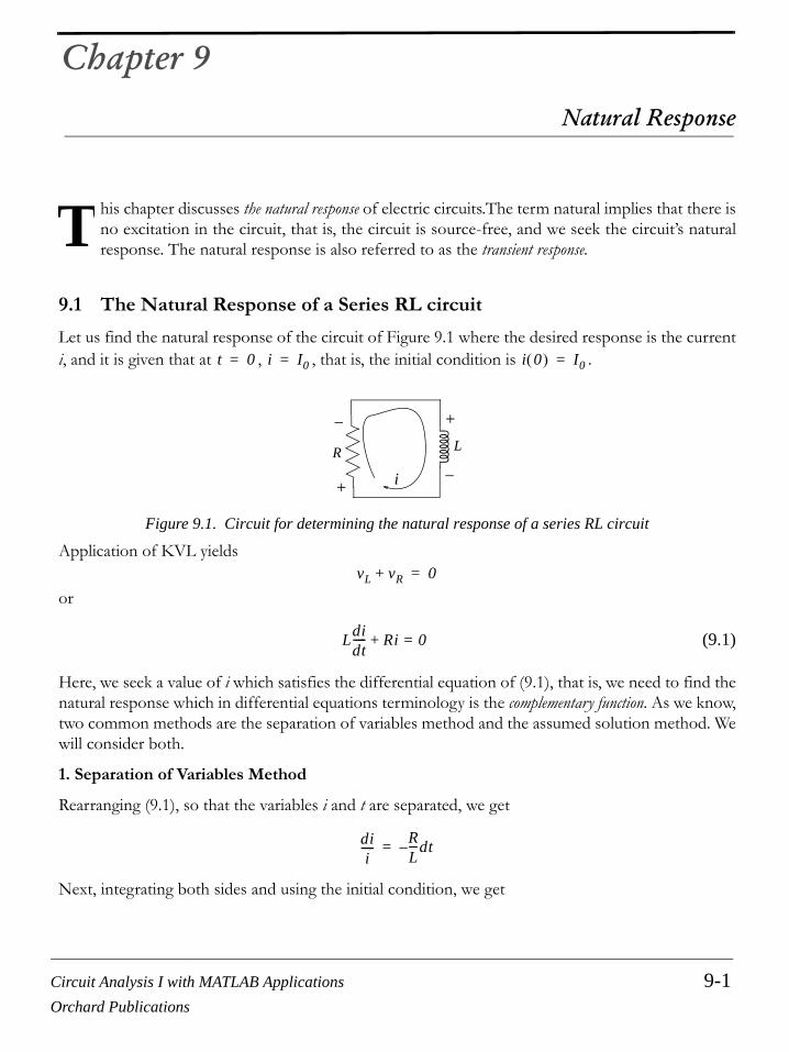
Circuit Analysis I with MATLAB Applications 9-1Orchard Publications
Chapter 9
Natural Response
his chapter discusses the natural response of electric circuits.The term natural implies that there isno excitation in the circuit, that is, the circuit is source-free, and we seek the circuit’s naturalresponse. The natural response is also referred to as the transient response.
9.1 The Natural Response of a Series RL circuit
Let us find the natural response of the circuit of Figure 9.1 where the desired response is the currenti, and it is given that at , , that is, the initial condition is .
Figure 9.1. Circuit for determining the natural response of a series RL circuit
Application of KVL yields
or
(9.1)
Here, we seek a value of i which satisfies the differential equation of (9.1), that is, we need to find thenatural response which in differential equations terminology is the complementary function. As we know,two common methods are the separation of variables method and the assumed solution method. Wewill consider both.
1. Separation of Variables Method
Rearranging (9.1), so that the variables i and t are separated, we get
Next, integrating both sides and using the initial condition, we get
T
t 0= i I0= i 0( ) I0=
+
+
R L
i −
−
vL vR+ 0=
Ldidt----- Ri+ 0=
dii
----- RL---dt–=

Chapter 9 Natural Response
9-2 Circuit Analysis I with MATLAB ApplicationsOrchard Publications
where is a dummy variable. Integration yields
or
or
Recalling that implies , we get
(9.2)
Substitution of (9.2) into (9.1) yields and that at , . Thus, both the differentialequation and the initial condition are satisfied.
2. Assumed Solution Method
Relation (9.1) indicates that the solution must be a function which, when added to its first derivativewill become zero. An exponential function will accomplish that and therefore, we assume a solutionof the form
(9.3)
where and are constants to be determined. Now, if (9.3) is a solution, it must satisfy the differen-tial equation (9.1). Then, by substitution, we get:
or
The left side of the last expression above will be zero if , or if , or if . But,if or , then every response is zero and this represents a trivial solution. Therefore,
is the only logical solution, and by substitution into (9.3) we get
1i--- id
I0
i∫
RL--- σd
0
t∫–=
σ
iln I0
i RL---σ 0
t–=
iln I0ln–RL---t–=
iI0----ln R
L---t–=
x yln= y ex=
i t( ) I0 e R L⁄( )t–=
0 0= t 0= i 0( ) I0=
i t( ) Aest=
A s
RAest sLAest+ 0=
s RL---+⎝ ⎠
⎛ ⎞ Aest 0=
A 0= s ∞–= s R L⁄–=
A 0= s ∞–=
s R L⁄–=
i t( ) Ae R L⁄( )t–=

Circuit Analysis I with MATLAB Applications 9-3Orchard Publications
The Natural Response of a Series RL circuit
We must now evaluate the constant . This is done with the use of the initial condition .
Thus, or and therefore,
as before. Next, we rewrite it as
(9.4)
and sketch it as shown in Figure 9.2.
Figure 9.2. Plot for in a series RL circuit
From Figure 9.2 we observe that at , , and as .
The initial rate (slope) of decay is found from the derivative of evaluated at , that is,
and thus the slope of the initial rate of decay is
Next, we define the time constant as the time required for to drop from unity to zero assum-ing that the initial rate of decay remains constant. This constant rate of decay is represented by thestraight line equation
and at , . Then,
A i 0( ) I0=
I0 Ae0= A I0=
i t( ) I0e R L⁄( )t–=
i t( )I0
-------- e R L⁄( )t–=
0.00.10.20.30.40.50.60.70.80.91.0
0 1 2 3 4 5Time Constants
Per
cent
i(t)
/ I 0 e−(R/L) t
5%
i(t) / I 0 = −(R / L) t +1
36.8%
13.5%
i t( ) I0⁄
t 0= i I0⁄ 1= i 0→ t ∞→
i I0⁄ t 0=
ddt----- i
I0----⎝ ⎠
⎛ ⎞
t 0=
RL---– e R L⁄( )t–
t 0=
RL---–= =
R L⁄–
τ i I0⁄
i t( )I0
-------- RL---t– 1+=
t τ= i I0⁄ 0=

Chapter 9 Natural Response
9-4 Circuit Analysis I with MATLAB ApplicationsOrchard Publications
or
(9.5)
Evaluating (9.4) at , we get
or
(9.6)
Therefore, in one time constant, the response has dropped to approximately 36.8% of its initial value.
If we express the rate of decay in time constant intervals as shown in Figure 9.2, we find that after , that is, it reaches its final value after five time constants.
Example 9.1
For the circuit shown in Figure 9.3, in how many seconds after has the
a. current has reached ½ of its initial value?
b. energy stored in has reached ¼ of its initial value?
c. power dissipated in has reached ¾ of its initial value?
Figure 9.3. Circuit for Example 9.1
Solution:
From (9.2),
where . Then,
0 RL---τ– 1+=
τ LR---=
Time Cons t for RL Circuittan
t τ L R⁄= =
i τ( )I0
--------- e R L⁄( )τ– e R L⁄( ) L R⁄( )– e 1– 0.368= = = =
i τ( ) 0.368I0=
i t( ) I0⁄ 0≈ t 5τ=
t 0=
i t( )
L
R
+
+
R
i −
−
10 ΩL
10 mH
i t( ) I0 e R L⁄( )t–=
I0 iL 0( )=

Circuit Analysis I with MATLAB Applications 9-5Orchard Publications
The Natural Response of a Series RL circuit
a. The current will have reached ½ of its initial value when
or
or
and therefore,
b. To find the energy stored in which reaches ¼ of its initial value, we start with
and at , . Then,
and
Therefore,
or
and
This is the same answer as in part (a) since the energy is proportional to the square of the current.
c. To find the power dissipated in when it reaches ¾ of its initial value, we start with the fact that
the instantaneous power absorbed by the resistor is , and since for the given circuit
then,
i t( )
0.5I0 I0e10 10 10 3–
×⁄( )t–I0e 1000t–
= =
e 1000t– 0.5=
1000t– 0.5( )ln 0.693–= =
t 693 µs=
L
WL t( ) 12---Li2 t( )=
t 0= I0 iL 0( )=
WL 0( ) 12---LI0
2=
14---WL 0( ) 1
4--- 1
2---LI0
2⎝ ⎠⎛ ⎞=
14---WL t( ) 1
2---Li2 t( ) 1
2---L I0 e R L⁄( )t–( )
2 14--- 1
2---LI0
2⎝ ⎠⎛ ⎞= = =
e 2 R L⁄( )t– 1 4⁄=
e 2000t– 1 4⁄=
2000t– 0.25( )ln 1.386–= =
t 693 µs=
R
pR iR2 R=
i t( ) iR t( ) I0 e R L⁄( )t–= =

Chapter 9 Natural Response
9-6 Circuit Analysis I with MATLAB ApplicationsOrchard Publications
and the energy dissipated (in the form of heat) in the resistor is
Also, from part (b) above,
and thus
or
and
In some examples and exercises that follow, the initial condition may not be given directly but it canbe found from the fact that the current through an inductor cannot change instantaneously andtherefore,
(9.7)
where will be used to denote the time just before a switch is opened or closed, and willbe used to denote the time just after the change has occurred.
Also, in our subsequent discussion, the expression “long time” will mean that sufficient time haselapsed so that the circuit has reached its steady-state conditions. As we know from Chapter 5, whenthe excitations are constant, at steady state conditions the inductor behaves as a short circuit, and thecapacitor behaves as an open circuit.
Example 9.2
In the circuit of Figure 9.4, the switch has been in the closed position for a long time and opens at
. Find for , , and
pR I02Re 2 R L⁄( )t–
=
WR pR td0
∞
∫ I02R e 2 R L⁄( )t– td
0
∞
∫ I02R L
2R-------–⎝ ⎠
⎛ ⎞ e 2 R L⁄( )t–
0
∞12---LI0
2= = = =
WL 0( ) 12---LI0
2=
34---WR
34---WL 0( ) 1
2---Li2 t( ) 1
2---L I0e R L⁄( )t–( )
2 34--- 1
2---LI0
2⎝ ⎠⎛ ⎞= = = =
e 2 R L⁄( )t– 3 4⁄=
e 2000t– 3 4⁄=
2000t– 0.75( )ln 0.288–= =
t 144 µs=
iL 0−( ) iL 0( ) iL 0+( )= =
iL 0−( ) iL 0+( )
S
t 0= iL t( ) t 0> vR 0−( ) vR 0+( )
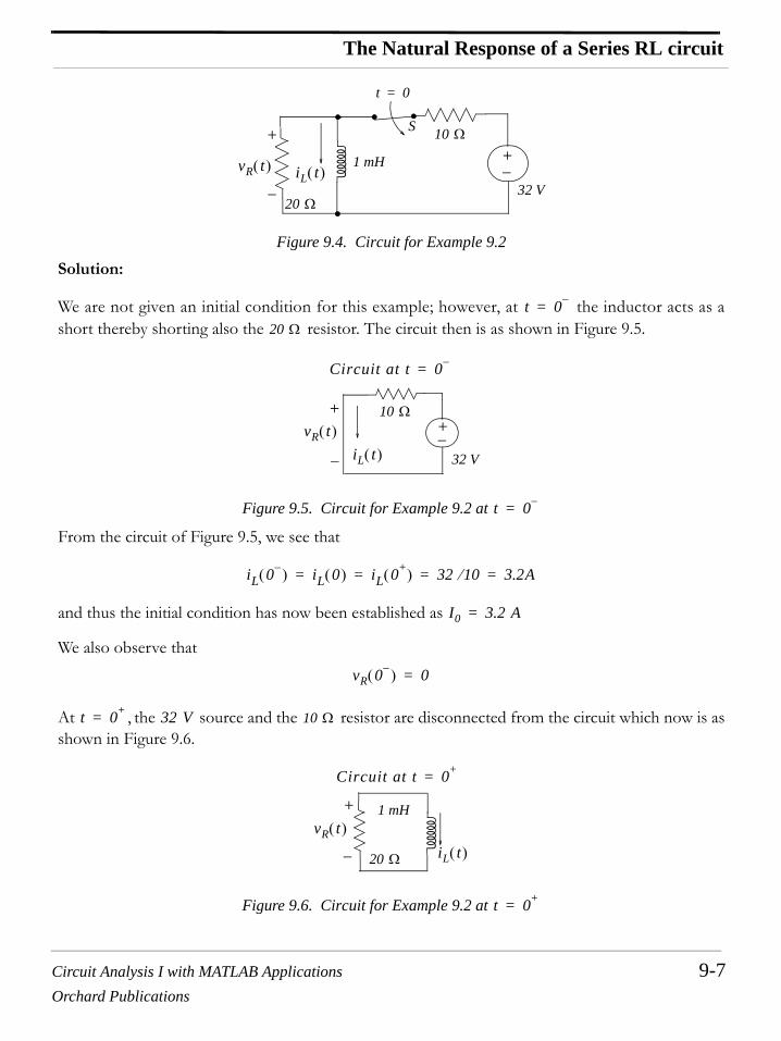
Circuit Analysis I with MATLAB Applications 9-7Orchard Publications
The Natural Response of a Series RL circuit
Figure 9.4. Circuit for Example 9.2
Solution:
We are not given an initial condition for this example; however, at the inductor acts as ashort thereby shorting also the resistor. The circuit then is as shown in Figure 9.5.
Figure 9.5. Circuit for Example 9.2 at
From the circuit of Figure 9.5, we see that
and thus the initial condition has now been established as
We also observe that
At , the source and the resistor are disconnected from the circuit which now is asshown in Figure 9.6.
Figure 9.6. Circuit for Example 9.2 at
32 V
+−
+
−
1 mH
S
20 Ω
iL t( )
10 Ω
vR t( )
t 0=
t 0−=20 Ω
32 V
+−
+
−
Circuit at t 0−=
vR t( )iL t( )
10 Ω
t 0−=
iL 0−( ) iL 0( ) iL 0+( ) 32 10⁄ 3.2A= = = =
I0 3.2 A=
vR 0−( ) 0=
t 0+= 32 V 10 Ω
+
−
1 mH
Circuit at t 0+=
20 Ω iL t( )vR t( )
t 0+=

Chapter 9 Natural Response
9-8 Circuit Analysis I with MATLAB ApplicationsOrchard Publications
For the circuit of Figure 9.6,
or
and
or
We observe that
Example 9.3
In the circuit shown in Figure 9.7, the switch has been closed for a long time and opens at .
Find:
a. for
b. at
c. at
Figure 9.7. Circuit for Example 9.3
Solution:
a. At the inductor acts as a short thereby shorting also the and resistors. The cir-cuit then is as shown in Figure 9.8. Then,
iL t( ) I0e R L⁄( )t– 3.2e20 10 3–⁄( )t–
= =
iL t( ) 3.2e 20000t–=
vR 0+( ) 20 I0–( ) 20 3.2–( )= =
vR 0+( ) 64 V–=
vR 0+( ) vR 0−( )≠
S t 0=
iL t( ) t 0>
i60 t( ) t 100 µs=
i48 t( ) t 200 µs=
72 V
+−
1 mH
S
t 0=
48 Ω
4 Ω 30 Ω
60 Ω
24 Ω
i60 t( )iL t( )
i48 t( )
t 0−= 24 Ω 48 Ω
iT 0−( ) 72 V4 60 || 30 +---------------------------- 72 V
4 20+--------------- 3 A= = =

Circuit Analysis I with MATLAB Applications 9-9Orchard Publications
The Natural Response of a Series RL circuit
Figure 9.8. Circuit for Example 9.3 at
and by the current division expression,
and thus the initial condition has been established as
At , the source and the resistor are disconnected from the circuit which now isas shown in Figure 9.9.
Figure 9.9. Circuit for Example 9.3 at
From (9.2),
where
and thus
or
72 V
+−
Circuit at t 0−=
30 Ω4 Ω
60 ΩiL 0−( )
iT 0−( )
t 0−=
iL 0−( ) 6030 60+------------------ iT 0−( )⋅ 6
9--- 3× 2 A= = =
I0 2 A=
t 0+= 72 V 4 Ω
1 mH
Circuit at t 0+=
iL t( )
48 Ω
i60 t( ) i48 t( )
60 Ω
30 Ω 24 Ω
t 0+=
iL t( ) I0eReq L⁄( )t–
=
Req 60 30+( ) || (24+48) 40 Ω= =
iL t( ) 2e 40 10 3–⁄( )t–=
iL t( ) 2e 40000t–=

Chapter 9 Natural Response
9-10 Circuit Analysis I with MATLAB ApplicationsOrchard Publications
Also,
or
and
or
9.2 The Natural Response of a Series RC Circuit
In this section, we will find the natural response of the circuit shown in Figure 9.10 where thedesired response is the capacitor voltage , and it is given that at , , that is, the initialcondition is .
Figure 9.10. Circuit for determining the natural response of a series RC circuit
By KCL,
(9.8)
and with
and
by substitution into (9.8), we obtain the differential equation
i60 t( )t 100 µs=
24 48+( )30 60+( ) 24 48+( )+
---------------------------------------------------- iL t( )–[ ]t 100 µs=
=
i60 t( )t 100 µs=
1227------ 2e 40000t––( )
t 100 µs=
89---e 4–– 16.3– mA= = =
i48 t( )t 200 µs=
30 60+( )30 60+( ) 24 48+( )+
---------------------------------------------------- iL t( )–[ ]t 200 µs=
=
i48 t( )t 200 µs=
1527------ 2e 40000t––( )
t 200 µs=
109
------e 8–– 0.373– mA= = =
RCvC t 0= vC V0=
v 0( ) V0=
R+
−C
iC
vC t( )
iR
iC iR+ 0=
iC CdvCdt
---------=
iRvCR-----=
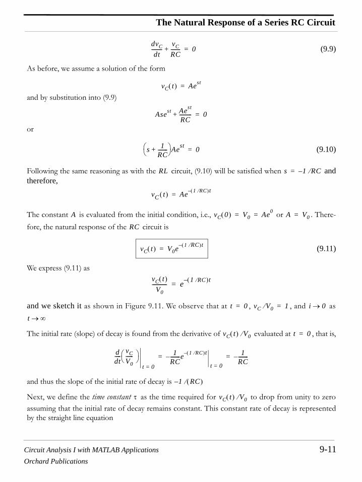
Circuit Analysis I with MATLAB Applications 9-11Orchard Publications
The Natural Response of a Series RC Circuit
(9.9)
As before, we assume a solution of the form
and by substitution into (9.9)
or
(9.10)
Following the same reasoning as with the circuit, (9.10) will be satisfied when andtherefore,
The constant is evaluated from the initial condition, i.e., or . There-fore, the natural response of the circuit is
(9.11)
We express (9.11) as
and we sketch it as shown in Figure 9.11. We observe that at , , and as
The initial rate (slope) of decay is found from the derivative of evaluated at , that is,
and thus the slope of the initial rate of decay is
Next, we define the time constant as the time required for to drop from unity to zeroassuming that the initial rate of decay remains constant. This constant rate of decay is representedby the straight line equation
dvCdt
---------vCRC--------+ 0=
vC t( ) Aest=
Asest Aest
RC----------+ 0=
s 1RC--------+⎝ ⎠
⎛ ⎞ Aest 0=
RL s 1 RC⁄–=
vC t( ) Ae 1 RC⁄( )t–=
A vC 0( ) V0 Ae0= = A V0=
RC
vC t( ) V0e 1 RC⁄( )t–=
vC t( )V0
------------ e 1 RC⁄( )t–=
t 0= vC V0⁄ 1= i 0→
t ∞→
vC t( ) V0⁄ t 0=
ddt-----
vCV0------⎝ ⎠
⎛ ⎞
t 0=
1RC--------– e 1 RC⁄( )t–
t 0=
1RC--------–= =
1 RC( )⁄–
τ vC t( ) V0⁄

Chapter 9 Natural Response
9-12 Circuit Analysis I with MATLAB ApplicationsOrchard Publications
Figure 9.11. Circuit for determining the natural response of a series RC circuit
(9.12)
and at , . Then,
or
(9.13)
Evaluating (9.11) at , we get
or
(9.14)
Therefore, in one time constant, the response has dropped to approximately 36.8% of its initial value.
If we express the rate of decay in time constant intervals as shown in Figure 9.11, we find that after , that is, it reaches its final value after five time constants.
In the examples that follow, we will make use of the fact that
(9.15)
0.00.10.20.30.40.50.60.70.80.91.0
0 1 2 3 4 5Time Constants
Per
cent
vc(t
) / V
0
e−(1/RC) t
5%
vc(t) / V0 = −(1/RC) t +1
36.8%
13.5%
vC t( )V0
------------- 1RC--------t– 1+=
t τ= vC t( ) V0⁄ 0=
0 1RC--------τ– 1+=
τ RC=
Time Cons t for RC Circuittan
t τ RC= =
vC τ( )V0
------------- e τ RC⁄– e RC RC⁄– e 1– 0.368= = = =
vC τ( ) 0.368V0=
vC t( ) V0⁄ 0≈ t 5τ=
vC 0−( ) vC 0( ) vC 0+( )= =
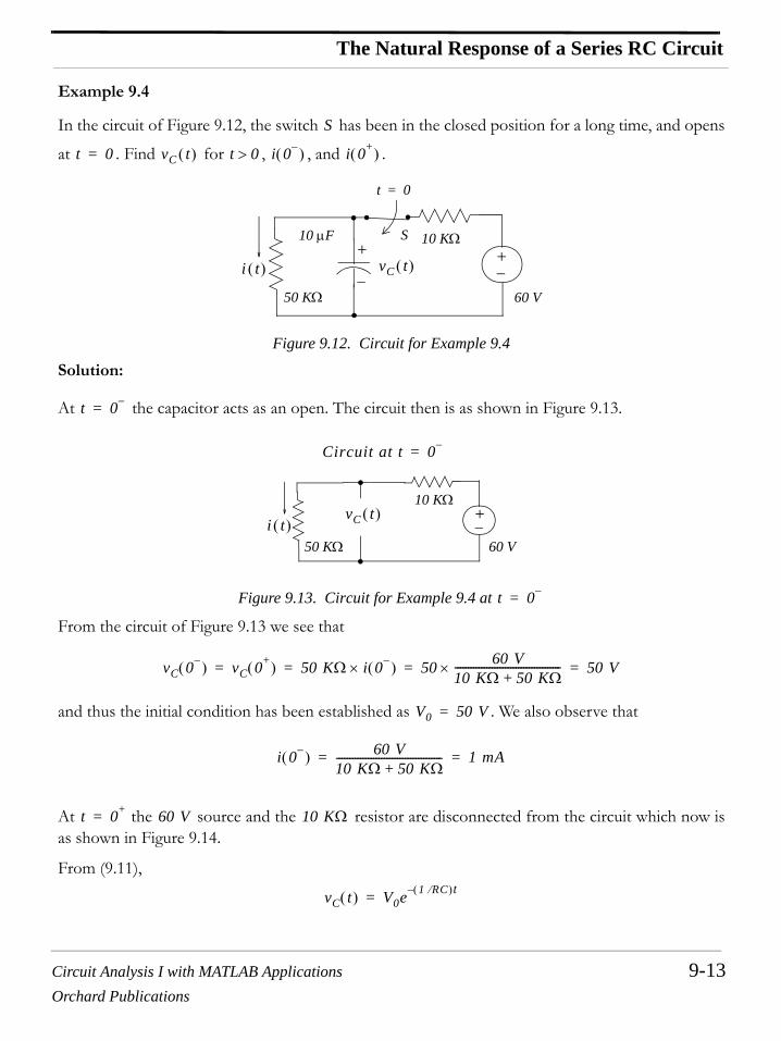
Circuit Analysis I with MATLAB Applications 9-13Orchard Publications
The Natural Response of a Series RC Circuit
Example 9.4
In the circuit of Figure 9.12, the switch has been in the closed position for a long time, and opens
at . Find for , , and .
Figure 9.12. Circuit for Example 9.4
Solution:
At the capacitor acts as an open. The circuit then is as shown in Figure 9.13.
Figure 9.13. Circuit for Example 9.4 at
From the circuit of Figure 9.13 we see that
and thus the initial condition has been established as . We also observe that
At the source and the resistor are disconnected from the circuit which now isas shown in Figure 9.14.
From (9.11),
S
t 0= vC t( ) t 0> i 0−( ) i 0+( )
60 V
10 KΩ
50 KΩ
+−
+
−
S10 µF
i t( ) vC t( )
t 0=
t 0−=
60 V
10 KΩ
50 KΩ
+−
Circuit at t 0−=
i t( )vC t( )
t 0−=
vC 0−( ) vC 0+( ) 50 KΩ i 0−( )× 50 60 V10 KΩ 50 KΩ+----------------------------------------× 50 V= = = =
V0 50 V=
i 0−( ) 60 V10 KΩ 50 KΩ+---------------------------------------- 1 mA= =
t 0+= 60 V 10 KΩ
vC t( ) V0e 1 RC⁄( )t–=
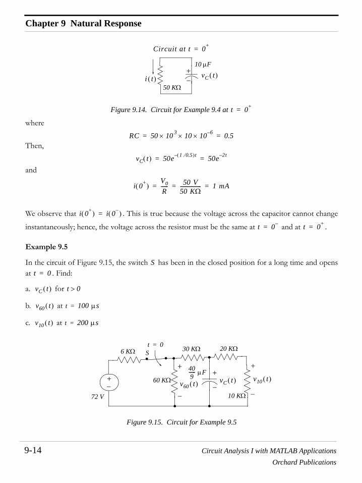
Chapter 9 Natural Response
9-14 Circuit Analysis I with MATLAB ApplicationsOrchard Publications
Figure 9.14. Circuit for Example 9.4 at
where
Then,
and
We observe that . This is true because the voltage across the capacitor cannot change
instantaneously; hence, the voltage across the resistor must be the same at and at .
Example 9.5
In the circuit of Figure 9.15, the switch has been in the closed position for a long time and opensat . Find:
a. for
b. at
c. at
Figure 9.15. Circuit for Example 9.5
50 KΩ
+−
10 µF
Circuit at t 0+=
i t( ) vC t( )
t 0+=
RC 50 10 3× 10 10 6–×× 0.5= =
vC t( ) 50e 1 0.5⁄( )t– 50e 2t–= =
i 0+( )V0R------ 50 V
50 KΩ----------------- 1 mA= = =
i 0+( ) i 0−( )=
t 0−= t 0+=
St 0=
vC t( ) t 0>
v60 t( ) t 100 µs=
v10 t( ) t 200 µs=
72 V
30 KΩ
60 KΩ+−
6 KΩ
10 KΩ
20 KΩS
+
−−
−
+ +
t 0=
v60 t( ) vC t( ) v10 t( )409
------ µF

Circuit Analysis I with MATLAB Applications 9-15Orchard Publications
The Natural Response of a Series RC Circuit
Solution:
a. At the capacitor acts as an open and the circuit then is as shown in Figure 9.16.
Figure 9.16. Circuit for Example 9.5 at
From the circuit of Figure 9.16,
and using the current division expression, we get
Then,
and thus the initial condition has been established as
At , the source and the resistor are disconnected from the circuit which nowis as shown in Figure 9.17.
Figure 9.17. Circuit for Example 9.5 at
t 0−=
72 V
30 KΩ
60 KΩ+−
6 KΩ
10 KΩ
20 KΩ
+
−−
−
+ +
Circuit at t 0−=
v60 t( ) vC t( ) v10 t( )
i10 t( )iT t( )
t 0−=
iT 0−( ) 72 V6 KΩ 60 KΩ 60 KΩ||+------------------------------------------------------------ 72 V
6 KΩ 30 KΩ+------------------------------------- 2 mA= = =
i10 0−( ) 60 KΩ60 KΩ 60 KΩ+---------------------------------------- iT 0−( )⋅ 1
2--- 2× 1 mA= = =
vC 0−( ) 20 KΩ 10 KΩ+( ) i10 0−( )⋅ 30 V= =
V0 30 V=
t 0+= 72 V 6 KΩ
30 KΩ
60 KΩ 10 KΩ
20 KΩ
+
−−
−
+ +
Circuit at t 0+=
vC t( )
409
------ µFv60 t( ) v10 t( )
t 0+=
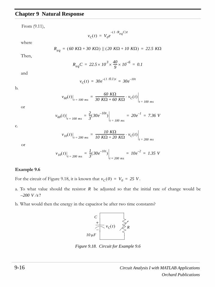
Chapter 9 Natural Response
9-16 Circuit Analysis I with MATLAB ApplicationsOrchard Publications
From (9.11),
where
Then,
and
b.
or
c.
or
Example 9.6
For the circuit of Figure 9.18, it is known that .
a. To what value should the resistor be adjusted so that the initial rate of change would be?
b. What would then the energy in the capacitor be after two time constants?
Figure 9.18. Circuit for Example 9.6
vC t( ) V0e1 ReqC⁄( )t–
=
Req 60 KΩ 30 KΩ+( ) || 20 KΩ 10 KΩ+( ) 22.5 KΩ= =
ReqC 22.5 10 3× 409
------ 10 6–×× 0.1= =
vC t( ) 30e 1 0.1⁄( )t– 30e 10t–= =
v60 t( )t 100 ms=
60 KΩ30 KΩ 60 KΩ+---------------------------------------- vC t( )⋅
t 100 ms=
=
v60 t( )t 100 ms=
23--- 30e 10t–( )
t 100 ms=
20e 1– 7.36 V= = =
v10 t( )t 200 ms=
10 KΩ10 KΩ 20 KΩ+---------------------------------------- vC t( )⋅
t 200 ms=
=
v10 t( )t 200 ms=
13--- 30e 10t–( )
t 200 ms=
10e 2– 1.35 V= = =
vC 0( ) V0 25 V= =
R200 V s⁄–
C
+−
10 µF
RvC t( )
Circuit Analysis I with MATLAB Applications 9-17Orchard Publications
Summary
Solution:
a. The capacitor voltage decays exponentially as
and with the given values,
Now, if the initial rate (slope) is to be , then
and solving for we get
b. After two time constants the capacitor voltage will drop to the value of
Therefore, the energy after two time constants will be
9.3 Summary
• The natural response of the inductor current in a simple circuit has the form
where denotes the value of the current in the inductor at
• In a simple circuit the time constant is the time required for to drop from unity tozero assuming that the initial rate of decay remains constant, and its value is
• In one time constant the natural response of the inductor current in a simple circuit hasdropped to approximately of its initial value.
• The natural response of the inductor current in a simple circuit reaches its final value, that is,it decays to zero, after approximately time constants.
• The initial condition can be established from the fact that the current through an inductor
cannot change instantaneously and thus
vC t( ) V0e 1 RC⁄( )t–=
vC t( ) 25e 100000 R⁄( )t–=
200 V s⁄–
dvCdt
---------t 0=
100000R
------------------–⎝ ⎠⎛ ⎞ 25e 100000 R⁄( )t–
t 0=
2.5 106×R
----------------------– 200–= = =
R R 12.5 KΩ=
vC 2τ( ) 25e 1 RC⁄( )2τ– 25e 2RC RC⁄( )– 25e 2– 3.38 V= = = =
WC t 2τ=
12---CvC
2 5 10 6–× 3.382× 57.2 µJ= = =
iL t( ) RL
iL t( ) I0 e R L⁄( )t–= I0 t 0=
RL τ iL t( ) I0⁄
τ L R⁄=
RL36.8%
RL5
I0
iL 0−( ) iL 0( ) iL 0+( )= =

Chapter 9 Natural Response
9-18 Circuit Analysis I with MATLAB ApplicationsOrchard Publications
• The natural response of the capacitor voltage in a simple circuit has the form
where denotes the value of the voltage across the capacitor at
• In a simple circuit the time constant is the time required for to drop from unity tozero assuming that the initial rate of decay remains constant, and its value is
• In one time constant the natural response of the capacitor voltage in a simple circuit hasdropped to approximately of its initial value.
• The natural response of capacitor voltage in a simple circuit reaches its final value, that is, itdecays to zero after approximately time constants.
• The initial condition can be established from the fact that the voltage across a capacitor cannot
change instantaneously and thus
vC t( ) RC
vC t( ) V0 e 1 RC⁄( )t–= V0 t 0=
RC τ vC t( ) V0⁄
τ RC=
RC36.8%
RC5
V0
vC 0−( ) vC 0( ) vC 0+( )= =

Circuit Analysis I with MATLAB Applications 9-19Orchard Publications
Exercises
9.4 Exercises
Multiple Choice
1. In a simple circuit the unit of the time constant is
A. dimensionless
B. the millisecond
C. the microsecondD. the reciprocal of second, i.e.,
E. none of the above
2. In a simple circuit the unit of the term is
A. the secondB. the reciprocal of second, i.e.,
C. the millisecond
D. the microsecond
E. none of the above
3. In the circuit of Figure 9.19 Switch has been closed for a long time while Switch has beenopen for a long time. At . Switch opens and Switch closes. The current for all
is
A.
B.
C.
D.
E. none of the above
Figure 9.19. Circuit for Question 3
RL τ
s 1–
RC 1 RC⁄
s 1–
S1 S2
t 0= S1 S2 iL t( )
t 0>
2 A
2e 100t– A
2e 50t– A
e 50t– A
t 0=
t 0=S1
S2
iL t( )
5 Ω
5 Ω2 A
100 mH

Chapter 9 Natural Response
9-20 Circuit Analysis I with MATLAB ApplicationsOrchard Publications
4. In the circuit of Figure 9.20 Switch has been closed for a long time while Switch has beenopen for a long time. At . Switch opens and Switch closes. The voltage for all
is
A.
B.
C.
D.
E. none of the above
Figure 9.20. Circuit for Question 4
5. In the circuit of Figure 9.21 Switch has been closed for a long time while Switch has beenopen for a long time. At . Switch opens and Switch closes. The power absorbed bythe inductor at will be
A.
B.
C.
D.
E. none of the above
Figure 9.21. Circuit for Question 5
S1 S2
t 0= S1 S2 vC t( )
t 0>
10 V
10e 10t– V
10e t– V
10e 0.1t– V
t 0=
t 0=S1
S2 vC t( )
50 KΩ 50 KΩ
10 V 20 µF
+ +−−
S1 S2
t 0= S1 S2
t +∞=
0 w
1 w
2 w
0.2 w
t 0=
t 0=S1
S2
iL t( )
5 Ω
5 Ω2 A
100 mH
Circuit Analysis I with MATLAB Applications 9-21Orchard Publications
Exercises
6. In the circuit of Figure 9.22 Switch has been closed for a long time while Switch has beenopen for a long time. At . Switch opens and Switch closes. The power absorbed bythe capacitor at will be
A.
B.
C.
D.
E. none of the above
Figure 9.22. Circuit for Question 6
7. In a simple circuit where and the time constant is
A.
B.
C.
D.
E. none of the above
8. In a simple circuit where and the time constant is
A.
B.
C.
D.
E. none of the above
9. In a simple circuit the condition(s) ___ are always true
S1 S2
t 0= S1 S2
t +∞=
0 w
10 w
5 w
10 mw
t 0=
t 0=S1
S2 vC t( )
50 KΩ 50 KΩ
10 V 20 µF
+ +−−
RL R 10 MΩ= L 10 µH= τ
1 s
100 s
1012 s
10 12– s
RC R 10 MΩ= C 10 µF= τ
100 s
0.01 s
100 µs
0.01 µs
RL

Chapter 9 Natural Response
9-22 Circuit Analysis I with MATLAB ApplicationsOrchard Publications
A. and
B. and
C. and
D.
E. none of the above.
10. In a simple circuit the condition(s) ___ are always true
A. and
B. and
C.
D. and
E. none of the above.
Problems
1. In the circuit of Figure 9.23, switch has been closed for a long time and switch has beenopen for a long time. Then, at switch opens while closes. Compute the current
through switch for
Figure 9.23. Circuit for Problem 1
2. In the circuit of Figure 9.24, both switches and have been closed for a long time and bothare opened at . Compute and sketch the current for the time interval
iL 0−( ) iL 0( ) iL 0+( )= = vL 0−( ) vL 0( ) vL 0+( )= =
iL 0−( ) iL 0( ) iL 0+( )= = iR 0−( ) iR 0( ) iR 0+( )= =
iL 0−( ) iL 0( ) iL 0+( )= = vR 0−( ) vR 0( ) vR 0+( )= =
iL 0−( ) iL 0( ) iL 0+( )= =
RC
vC 0−( ) vC 0( ) vC 0+( )= = iC 0−( ) iC 0( ) iC 0+( )= =
vC 0−( ) vC 0( ) vC 0+( )= = vR 0−( ) vR 0( ) vR 0+( )= =
vC 0−( ) vC 0( ) vC 0+( )= =
vC 0−( ) vC 0( ) vC 0+( )= = iR 0−( ) iR 0( ) iR 0+( )= =
S1 S2
t 0= S1 S2
iS2 t( ) S2 t 0>
15 V
8 Ω
6 Ω+−
2.5 mH
3 Ω
10 Ω
5 Ω
iS2 t( )
t 0=
t 0=
S2
S1
S1 S2
t 0= iL t( ) 0 t 1 ms≤ ≤

Circuit Analysis I with MATLAB Applications 9-23Orchard Publications
Exercises
Figure 9.24. Circuit for Problem 2
3. In a series circuit, the voltage across the inductor is and the current at is . Compute the values of and for that circuit.
4. In the circuit of Figure 9.25, both switches and have been closed for a long time, whileswitch has been open for a long time. At and are opened and is closed.Compute the current for .
Figure 9.25. Circuit for Problem 4
5. In the circuit of Figure 9.26, switch has been closed and has been open for a long time. At switch is opened and is closed. Compute the voltage for .
24 V
8 Ω16 Ω
+− 4 Ω
10 Ω
12 Ω
+ −
12 V
6 Ω
iL t( )t 0=
t 0=S1
S2
10 3 mH⁄
2 Ω
RL vL vL 0.2e 2000t– V= iL
t 0= iL 0( ) 10 mA= R L
S1 S2
S3 t 0= S1 S2 S3
iL t( ) t 0>
+
−
+
−
+
−+
−10 mV
1 KΩ
2 KΩ
20 mV
3 mH
10 KΩ
10 KΩ5 KΩ
iL t( )
vin1
vout
t 0= t 0=
t 0= S3
S1
S2
vin2
S1 S2
t 0= S1 S2 vC2 t( ) t 0>

Chapter 9 Natural Response
9-24 Circuit Analysis I with MATLAB ApplicationsOrchard Publications
Figure 9.26. Circuit for Problem 5
6. In the circuit of Figure 9.27, switch has been in the position for a long time and at isthrown in the position. Compute the voltage across the capacitor for , and theenergy stored in the capacitor at .
Figure 9.27. Circuit for Problem 6
7. In the circuit of Figure 9.28, switch has been open for a long time and closes at . Compute for
Figure 9.28. Circuit for Problem 7
12 V
10 KΩ 50 KΩ
+−
+−
6 µF
10 KΩ
3 µF
+
−
t 0=t 0=
vC2 t( )vC1 t( )
S1 S2
S A t 0=
B vC t( ) t 0>
t 1 ms=
24 V
16 KΩ4 KΩ
+−
+
−
S
5 µF
2 KΩ A
B
8 KΩ 6 KΩ
t 0=
vC t( )
S t 0=
iSW t( ) t 0>
36 V
S
100 Ω
3 Ω
6 Ω
10 µF6 mH
+−
iSW t( )t 0=

Circuit Analysis I with MATLAB Applications 9-25Orchard Publications
Answers to Exercises
9.5 Answers to Exercises
Multiple Choice
1. E
2. B
3. D
4. C
5. A
6. A
7. D
8. B
9. D
10. C
Problems
1. The circuit at is as shown below.
Replacing the circuit above with its Thevenin equivalent to the left of points and we find
that and and attaching the rest of the circuit
to it we get the circuit below.
By voltage-source to current-source transformation we get the circuit below.
τ L R⁄ volt ampere ondsec⁄( )⁄[ ] volt ampere⁄[ ]⁄ ond s( )sec= = =
t 0−=
15 V
8 Ω
6 Ω+−
3 Ω
10 Ω
5 Ω
×
×x
yiL 0−( )
x y
vTH6
3 6+------------ 15⋅ 10 V= = RTH
3 6×3 6+------------ 8+ 10 Ω= =
10 V
10 Ω+−
10 Ω
vTHRTH
5 Ω
iL 0−( )

Chapter 9 Natural Response
9-26 Circuit Analysis I with MATLAB ApplicationsOrchard Publications
and by inspection, , that is, the initial condition has been established as
The circuit at is as shown below.
We observe that the closed shorts out the and resistors and the circuit simplifies to thatshown below.
Thus for ,
2. The circuit at is as shown below and the mesh equations are
Then,
10 Ω
5 ΩiL 0−( )
5 Ω
10 Ω
1 A
iL 0−( ) 0.5 A=
iL 0−( ) iL 0( ) iL 0+( ) I0 0.5 A= = = =
t 0+=
8 Ω
6 Ω
2.5 mH
5 Ω
iS2 t( )
ClosedSwitch
iL 0+( ) 0.5 A=
6 Ω 8 Ω
2.5 mH
5 Ω
iS2 t( )iL 0+( ) I0 0.5 A= =
t 0> iS2 t( ) iL t( )– I0e R L⁄( )t–– 0.5e 5 2.5 10 3–×⁄( )t–– 0.5e 2000t– A–= = = =
t 0−=
20i1 4i3 – 24=
16i2 6i3– 8i4– 12–=
4i1– 6i2– 20i3 10i4–+ 0=
8i2 10i3– 30i4+ 0=
iL 0−( ) i3 i4–=

Circuit Analysis I with MATLAB Applications 9-27Orchard Publications
Answers to Exercises
and with MATLAB
R=[20 0 −4 0; 0 16 −6 −8; −4 −6 20 −10; 0 −8 −10 30];...V=[24 −12 0 0]'; I=R\V; iL0=I(3)-I(4); fprintf(' \n');...fprintf('i1 = %4.2f A \t', I(1)); fprintf('i2 = %4.2f A \t', I(2));...fprintf('i3 = %4.2f A \t', I(3)); fprintf('i4 = %4.2f A \t', I(4));...fprintf('iL0 = %4.2f A \t', I(3)−I(4)); fprintf(' \n'); fprintf(' \n');
i1 = 1.15 A i2 = -1.03 A i3 = -0.26 A i4 = -0.36 A iL0 = 0.10 A
Therefore,
Shown below is the circuit at and the steps of simplification.
Thus for ,
and
24 V
8 Ω
16 Ω
+− 4 Ω
10 Ω
12 Ω
+ −
12 V
6 ΩiL 0−( )
2 Ω
i4
i3
i2
i1
iL 0−( ) iL 0( ) iL 0+( ) I0 0.1 A= = = =
t 0+=
6 Ω
4 Ω
8 Ω
iL 0+( ) 103 ------mH
10 Ω12 Ω
10 Ω 20 Ω10 Ω
103 ------mH
iL 0+( )
20/3 Ω
20/3 Ω
iL 0+( )
103 ------mH
t 0>
iL t( ) I0e R L⁄( )t– 0.1e 5000t– A= =
iL t 0.4 ms=0.1e 2– 0.0137 A 13.7 mA= = =

Chapter 9 Natural Response
9-28 Circuit Analysis I with MATLAB ApplicationsOrchard Publications
To compute and sketch the current for the time interval we use MATLAB asshown below.
t=(0: 0.01: 1)*10^(−3);...iLt=0.1.*10.^(−3).*exp(−5000.*t);...plot(t,iLt); grid
3. From the figure below for
and with , by substitution
or Also, from ,
4. The circuit at is as shown below and using the relation
that was developed in Example 4.11 we have
iL t( ) 0 t 1 ms≤ ≤
0 0.1 0.2 0.3 0.4 0.5 0.6 0.7 0.8 0.9 1
x 10-3
0
0.2
0.4
0.6
0.8
1x 10
-4
vL RiL 0.2e 2000t–= = t 0>
iL
vL
++
− −
R L
iL 0( ) 10 mA= R 10 10 3–×( ) 0.2e 0– 0.2= =
R 0.2 10 2–⁄ 20 Ω= = R L⁄ 2000= L 20 2000⁄ 0.01 10 mH= = =
t 0−=
vout Rfvin1Rin1----------
vin2Rin2----------+
⎝ ⎠⎜ ⎟⎛ ⎞
–=

Circuit Analysis I with MATLAB Applications 9-29Orchard Publications
Answers to Exercises
and
The circuit at is as shown below where with the direction shown.
Then for
with the direction shown.
5. The circuit at is as shown below. As we’ve learned in Chapter 5, when a circuit is excitedby a constant (DC) source, after sufficient time has elapsed the capacitor behaves as an open andthus the voltage across the capacitor is as shown.
+
−
+
−
+
−+
−10 mV
1 KΩ
2 KΩ
20 mV
10 KΩ
5 KΩ
iL
vin2vout
vin1
vout 10 KΩ 10 2–
1 KΩ-------------- 2 10 2–×
2 KΩ--------------------+⎝ ⎠
⎛ ⎞– 10 2 10 2–××– 0.2 V–= = =
iL 0−( ) I0 i5 KΩ0.2 V–
5 KΩ---------------- 40 10 6–× A– 40 µA–= = = = =
t 0+= iL 0+( ) 40 µA=
10 KΩ
3 mH
5 KΩ
iL 0+( )
+
+
−
−
0.2V
3 mH
15 KΩiL 0+( ) ++
−−
t 0>
iL t( ) I0e R L⁄( )t 40 10 6–× e 15 103× 3 10 3–×⁄( )t 40e 5 106t×– µA= = =
t 0−=
C1 12 V

Chapter 9 Natural Response
9-30 Circuit Analysis I with MATLAB ApplicationsOrchard Publications
The circuit at is as shown below where the represents the voltage across capacitor.
Now, where and
Then, and thus
6. The circuit at is as shown below.
Then,
The circuit at is as shown below where .
12 V
10 KΩ
+− 6 µF
10 KΩ
+
−vC1 0−( ) 12V=
C1
t 0+= 12 VC1
12 V
50 KΩ
+− +
−6 µF
3 µF+
−
vC2 t( )C1
C2
vC1
vC2 t( ) vC1e1 RCeq⁄( )–
= vC1 12 V= CeqC1 C2⋅C1 C2+------------------ 6 3×
6 3+------------ 2 µF= = =
1 RCeq⁄ 1 5 104× 2 10 6–××( )⁄ 10= = vC2 t( ) 12e 10t–=
t 0−=
24 V
16 KΩ4 KΩ
+−
+
−
5 µF
2 KΩ
6 KΩ vC 0−( )
vC 0−( ) V0 v6KΩ6 KΩ
6 KΩ 6 KΩ+---------------------------------- 24× 12 V= = = =
t 0+= vC 0+( ) 12 V=

Circuit Analysis I with MATLAB Applications 9-31Orchard Publications
Answers to Exercises
Series and parallel resistances reduction yields
and the circuit for reduces to the one shown below.
Now, , and . Also,
7. The circuit at is as shown below.
Then, and
16 KΩ4 KΩ
+
−
5 µF
8 KΩ 6 KΩvC 0+( )
Req 8 KΩ 4 KΩ+( ) 6 KΩ||[ ] 16 KΩ+ 12 6×12 6+--------------- 16+ 4 16+ 20 KΩ= = = =
t 0>
+
−
5 µF
20 KΩvC t( )
ReqC 2 104× 5 10 6–×× 0.1= = 1 ReqC⁄ 10= vC t( ) V0e 10t– 12e 10t–= =
WC 1 ms
12---CvC
2 t( )1 ms
0.5 5 10 6–×× 144e 20t–× t 1 ms== =
360 10 6–× e 20t–t 1 ms=
0.35 mJ==
t 0−=
36 V
100 Ω
3 Ω
6 Ω
+−
iL 0−( )
+
−
vC 0−( )
iL 0−( ) 36 V6 3+( ) Ω
------------------------ 4 A= = vC 0−( ) 3 iL 0−( )× 3 4× 12 V= = =

Chapter 9 Natural Response
9-32 Circuit Analysis I with MATLAB ApplicationsOrchard Publications
The circuit at is as shown below and the current through the switch is the sum of
the currents due to the voltage source, due to , and due to .
We will apply superposition three times. Thus for :
I. With the voltage source acting alone where (open) and (shorted), the cir-cuit is as shown below.
Since the is shorted out, we have
II. With the current source acting alone the circuit is as shown below where weobserve that the and resistors are shorted out and thus where
, , , , and thus
t 0+= iSW t( )
36 V iL 0+( ) 4 A= vC 0+( ) 12 V=
36 V
100 Ω
3 Ω
6 Ω
10 µF6 mH+
− iSW t( ) vC 0+( ) 12 V=−
+iL 0+( ) 4 A=
t 0>
36 V iL 0= vC 0=
36 V
100 Ω
3 Ω
6 Ω
6 mH+− i'SW t( )
vC t( ) 0=
iL t( ) 0=
100 Ω
i'SW t( ) 36 6⁄ 6 A= =
iL 0+( ) 4 A=
6 Ω 100 Ω i''SW t( ) iL t( )–=
iL t( ) I0e R L⁄( )t–= I0 4 A= R 3 Ω= L 6 mH= R L⁄ 3 6 10 3–×( )⁄ 500= =
i''SW t( ) iL t( )– 4e 500t––= =
Circuit Analysis I with MATLAB Applications 9-33Orchard Publications
Answers to Exercises
III. With the voltage source acting alone the circuit is as shown belowwhere we observe that the resistor is shorted out.
and thus
. Then,
Therefore, the total current through the closed switch for is
100 Ω
3 Ω
6 Ω
6 mH iSW t( )
vC t( ) 0 V=
iL 0+( ) 4 A=
vC 0+( ) V0= 12 V=
6 Ω
100 Ω
3 Ω
6 Ω
6 mH i'''SW t( )
vC 0+( ) 12 V=
iL t( ) 0=
vC t( ) V0e 1 RC⁄( )t– 12e 1 100 10 5–×( )⁄[ ]t– 12e 1000t–= = =
i'''SW t( ) vC t( ) 100 Ω⁄ 0.12e 1000t–= =
t 0>
iSW t( ) i'SW t( ) i''SW t( ) i'''SW t( )+ + 6 4e 500t–– 0.12e 1000t– A+= =

Chapter 9 Natural Response
9-34 Circuit Analysis I with MATLAB ApplicationsOrchard Publications
NOTES

Circuit Analysis I with MATLAB Applications 10-1Orchard Publications
Chapter 10
Forced and Total Response in RL and RC Circuits
his chapter discusses the forced response of electric circuits.The term “forced” here impliesthat the circuit is excited by a voltage or current source, and its response to that excitation isanalyzed. Then, the forced response is added to the natural response to form the total
response.
10.1 The Unit Step Function
A function is said to be discontinuous if it exhibits points of discontinuity, that is, if the function jumpsfrom one value to another without taking on any intermediate values.
A well-known discontinuous function is the unit step function * that is defined as
(10.1)
It is also represented by the waveform of Figure 10.1.
Figure 10.1. Waveform for
In the waveform of Figure 10.1, the unit step function changes abruptly from 0 to 1 at .But if it changes at instead, its waveform and definition are as shown in Figure 10.2.
Figure 10.2. Waveform and definition of
* In some books, the unit step function is denoted as ,that is, without the subscript 0. In this text we will reservethis designation for any input.
Tu0 t( )
u0 t( )
u t( )
u0 t( )0 t 0<1 t 0>⎩
⎨⎧
=
1
0
u0 t( )
u0 t( )
u0 t( ) t 0=
t t0=
u0 t t0–( )0 t t0<
1 t t0>⎩⎨⎧
=1
t0 t
0
u0 t t0–( )
u0 t t0–( )

Chapter 10 Forced and Total Response in RL and RC Circuits
10-2 Circuit Analysis I with MATLAB ApplicationsOrchard Publications
Likewise, if the unit step function changes from to at as shown in Figure 10.3, it isdenoted as
Figure 10.3. Waveform and definition of
Other forms of the unit step function are shown in Figure 10.4.
Figure 10.4. Other forms of the unit step function
Unit step functions can be used to represent other time-varying functions such as the rectangularpulse shown in Figure 10.5. This pulse is represented as .
Figure 10.5. A rectangular pulse expressed as the sum of two unit step functions
0 1 t t0–=
u0 t t0+( )
u0 t t0+( )0 t t0–<
1 t t0–>⎩⎨⎧
=t−t0 0
1 u0 t t0+( )
u0 t t0+( )
0t
t
t tΤ −Τ
0
00
0 Τ
0
0
t
tt
0 0t t
−Τ
−ΤΤ
(a) (b) (c)
(d) (e) (f)
(g) (h) (i)
−A −A −A
−A −A −A
A A AAu0 t–( )
A– u0 t( ) A– u0 t T–( ) A– u0 t T+( )
Au0 t– T+( ) Au0 t– T–( )
A– u0 t–( ) A– u0 t– T+( ) A– u0 t– T–( )
u0 t( ) u0 t 1–( )–
0 0 0t t t
1
1
1u0 t( )
u0 t 1–( )–
u0 t( ) u0 t 1–( )–

Circuit Analysis I with MATLAB Applications 10- 3Orchard Publications
The Unit Step Function
The unit step function offers a convenient method of describing the sudden application of a voltageor current source. For example, a constant voltage source of applied at , can be denotedas . Likewise, a sinusoidal voltage source that is applied to a circuit at
, can be described as . Also, if the excitation in a circuit is arectangular, or triangular, or sawtooth, or any other recurring pulse, it can be represented as a sum(difference) of unit step functions.
Example 10.1
Express the square waveform of Figure 10.6 as a sum of unit step functions. The vertical dottedlines indicate the discontinuities at , and so on.
Figure 10.6. Square waveform for Example 10.1
Solution:
The line segment has height , starts at , and terminates at on the time axis. Then,as in Figure 10.5, this segment can be expressed as
(10.2)
The line segment has height , starts at , on the time axis, and terminates at . Thissegment can be expressed as
(10.3)
Line segment has height , starts at , and terminates at . This segment can beexpressed as
(10.4)
Line segment has height , starts at , and terminates at . This segment can beexpressed as
(10.5)
Thus, the square waveform of Figure 10.6 can be expressed as the summation of (10.2) through(10.5), that is,
24 V t 0=
24u0 t( ) V v t( ) Vm ωt Vcos=
t t0= v t( ) Vm ωtcos( )u0 t t0–( ) V=
T 2T 3T,,
A
−A
tT 3T2T0
v t( )
A t 0= t T=
v1 t( ) A u0 t( ) u0 t T–( )–[ ]=
A– t T= t 2T=
v2 t( ) A– u0 t T–( ) u0 t 2T–( )–[ ]=
A t 2T= t 3T=
v3 t( ) A u0 t 2T–( ) u0 t 3T–( )–[ ]=
A– t 3T= t 4T=
v4 t( ) A– u0 t 3T–( ) u0 t 4T–( )–[ ]=

Chapter 10 Forced and Total Response in RL and RC Circuits
10-4 Circuit Analysis I with MATLAB ApplicationsOrchard Publications
(10.6)
Combining like terms, we get
(10.7)
Example 10.2
Express the symmetric rectangular pulse of Figure 10.7 as a sum of unit step functions.
Figure 10.7. Symmetric rectangular pulse for Example 10.2
Solution:
This pulse has height , it starts at , and terminates at . Therefore, with referenceto Figures 10.3 and 10.4 (b), we get
(10.8)
Example 10.3
Express the symmetric triangular waveform shown in Figure 10.8 as a sum of unit step functions.
Figure 10.8. Symmetric triangular waveform for Example 10.3
Solution:
As a first step, we derive the equations of the linear segments and shown in Figure 10.9.
v t( ) v1 t( ) v2 t( ) v3 t( ) v4 t( )+ + +=
A u0 t( ) u0 t T–( )–[ ] A– u0 t T–( ) u0 t 2T–( )–[ ]=
+A u0 t 2T–( ) u0 t 3T–( )–[ ] A– u0 t 3T–( ) u0 t 4T–( )–[ ]
v t( ) A u0 t( ) 2u0 t T–( )– 2u0 t 2T–( ) 2u0 t 3T–( )– …+ +[ ]=
A
−T/2t
0 T/2
i t( )
A t T 2⁄–= t T 2⁄=
i t( ) Au0 t T2---+⎝ ⎠
⎛ ⎞ Au0 t T2---–⎝ ⎠
⎛ ⎞– A u0 t T2---+⎝ ⎠
⎛ ⎞ u0 t T2---–⎝ ⎠
⎛ ⎞–= =
1
−T/2t
0 T/2
v t( )

Circuit Analysis I with MATLAB Applications 10- 5Orchard Publications
The Unit Step Function
Figure 10.9. Equations for the linear segments of Figure 10.8
For line segment ,
(10.9)
and for line segment ,
(10.10)
Combining (10.9) and (10.10), we get
(10.11)
Example 10.4
Express the waveform shown in Figure 10.10 as a sum of unit step functions.
Figure 10.10. Waveform for Example 10.4
Solution:
As in the previous example, we first find the equations of the linear segments and shown inFigure 10.11.
1
−T/2t
0 T/2
2T--- t 1+
2T---– t 1+
v t( )
v1 t( ) 2T--- t 1+⎝ ⎠
⎛ ⎞ u0 t T2---+⎝ ⎠
⎛ ⎞ u0 t( )–=
v2 t( ) 2T---– t 1+⎝ ⎠
⎛ ⎞ u0 t( ) u0 t T2---–⎝ ⎠
⎛ ⎞–=
v t( ) v1 t( ) v2 t( )+=
2T--- t 1+⎝ ⎠
⎛ ⎞ u0 t T2---+⎝ ⎠
⎛ ⎞ u0 t( )– 2T---– t 1+⎝ ⎠
⎛ ⎞ u0 t( ) u0 t T2---–⎝ ⎠
⎛ ⎞–+=
t
1
2
3
1 2 30
v t( )

Chapter 10 Forced and Total Response in RL and RC Circuits
10-6 Circuit Analysis I with MATLAB ApplicationsOrchard Publications
Figure 10.11. Equations for the linear segments of Figure 10.10
Following the same procedure as in the previous examples, we get
Multiplying the values in parentheses by the values in the brackets, we get
or
and combining terms inside the brackets, we get
(10.12)
Two other functions of interest are the unit ramp function and the unit impulse or delta function. Wewill discuss the unit ramp function first.
10.2 The Unit Ramp Function
The unit ramp function, denoted as , is defined as
(10.13)
where τ is a dummy variable.
t
1
2
3
1 2 30
v t( )
2t 1+ t– 3+
v t( ) 2t 1+( ) u0 t( ) u0 t 1–( )–[ ] 3 u0 t 1–( ) u0 t 2–( )–[ ]+=
+ t– 3+( ) u0 t 2–( ) u0 t 3–( )–[ ]
v t( ) 2t 1+( )u0 t( ) 2t 1+( )u0 t 1–( )– 3u0 t 1–( )+=
3u0 t 2–( )– t– 3+( )u0 t 2–( ) t– 3+( )u0 t 3–( )–+
v t( ) 2t 1+( )u0 t( ) 2t 1+( )– 3+[ ]u0 t 1–( )+=
+ 3– t– 3+( )+[ ]u0 t 2–( ) t– 3+( )u0 t 3–( )–
v t( ) 2t 1+( )u0 t( ) 2 t 1–( )u0 t 1–( )– t– u0 t 2–( ) t 3–( )u0 t 3–( )+=
u1 t( )
u1 t( )
u1 t( ) u0 τ( ) τd∞–
t
∫=

Circuit Analysis I with MATLAB Applications 10- 7Orchard Publications
The Unit Ramp Function
We can evaluate the integral of (10.13) by considering the area under the unit step function from to as shown in Figure 10.12.
Figure 10.12. Area under the unit step function from to
Therefore,
(10.14)
and since is the integral of , then must be the derivative of , i.e.,
(10.15)
Higher order functions of can be generated by repeated integration of the unit step function. Forexample, integrating twice and multiplying by , we define as
(10.16)
Similarly,
(10.17)
and in general,
(10.18)
Also,
(10.19)
u0 t( )
∞– t
tτ
1Area 1τ τ t= = =
∞– t
u1 t( )0 t 0<t t 0≥⎩
⎨⎧
=
u1 t( ) u0 t( ) u0 t( ) u1 t( )
ddt-----u1 t( ) u0 t( )=
tu0 t( ) 2 u2 t( )
u2 t( )0 t 0<
t2 t 0≥⎩⎨⎧
= or u2 t( ) 2 u1 τ( ) τd∞–
t
∫=
u3 t( )0 t 0<
t3 t 0≥⎩⎨⎧
= or u3 t( ) 3 u2 τ( ) τd∞–
t
∫=
un t( )0 t 0<
t n t 0≥⎩⎨⎧
= or un t( ) 3 un 1– τ( ) τd∞–
t
∫=
un 1– t( ) 1n--- d
dt-----un t( )=
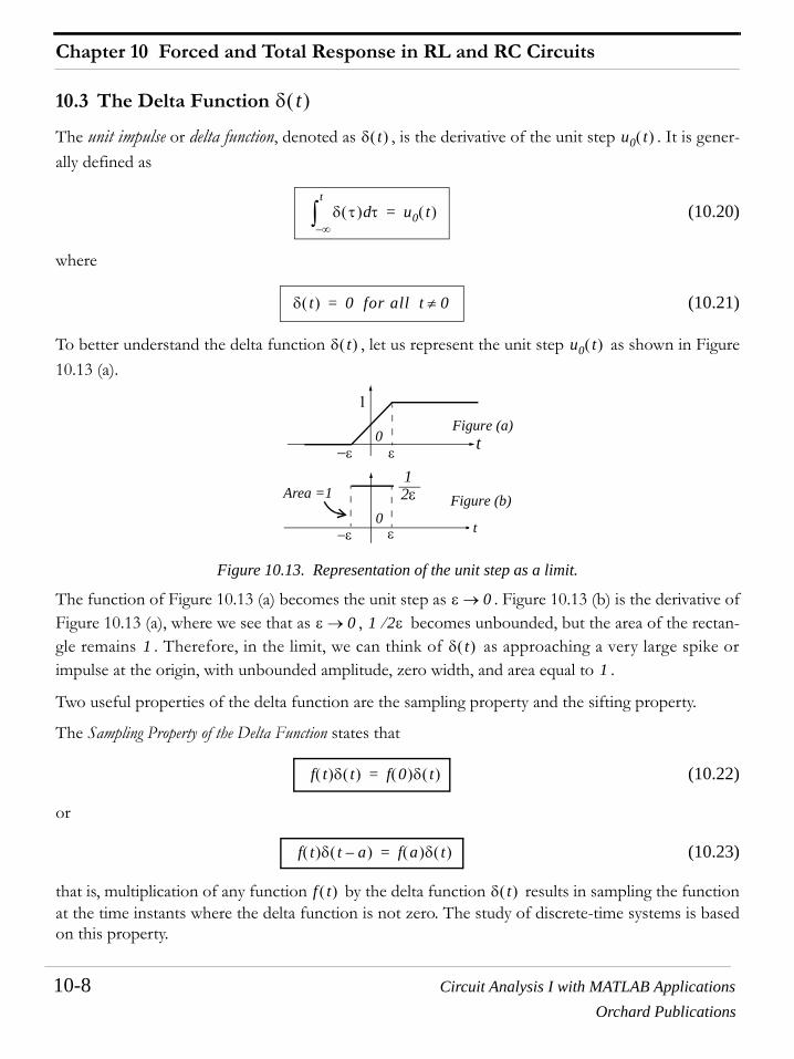
Chapter 10 Forced and Total Response in RL and RC Circuits
10-8 Circuit Analysis I with MATLAB ApplicationsOrchard Publications
10.3 The Delta Function
The unit impulse or delta function, denoted as , is the derivative of the unit step . It is gener-ally defined as
(10.20)
where
(10.21)
To better understand the delta function , let us represent the unit step as shown in Figure10.13 (a).
Figure 10.13. Representation of the unit step as a limit.
The function of Figure 10.13 (a) becomes the unit step as . Figure 10.13 (b) is the derivative ofFigure 10.13 (a), where we see that as , becomes unbounded, but the area of the rectan-gle remains . Therefore, in the limit, we can think of as approaching a very large spike orimpulse at the origin, with unbounded amplitude, zero width, and area equal to .
Two useful properties of the delta function are the sampling property and the sifting property.
The Sampling Property of the Delta Function states that
(10.22)
or
(10.23)
that is, multiplication of any function by the delta function results in sampling the functionat the time instants where the delta function is not zero. The study of discrete-time systems is basedon this property.
δ t( )
δ t( ) u0 t( )
δ τ( ) τd∞–
t
∫ u0 t( )=
δ t( ) 0 for all t 0≠=
δ t( ) u0 t( )
−ε ε
12ε
Figure (a)
Figure (b)Area =1
ε−ε
1
t
t0
0
ε 0→ε 0→ 1 2⁄ ε
1 δ t( )1
f t( )δ t( ) f 0( )δ t( )=
f t( )δ t a–( ) f a( )δ t( )=
f t( ) δ t( )

Circuit Analysis I with MATLAB Applications 10- 9Orchard Publications
The Delta Function
The Sifting Property of the Delta Function states that
(10.24)
that is, if we multiply any function by and integrate from −∞ to +∞, we will obtain thevalue of evaluated at .
The proofs of (10.22) through (10.24) and additional properties of the delta function are beyond thescope of this book. They are provided in Signals and Systems with MATLAB Applications, ISBN 0-9709511-3-2 by this author, Orchard Publications 2001.
MATLAB has two built-in functions for the unit step and the delta functions. These are designatedby the names of the mathematicians who used them in their work. The unit step is calledHeavyside(t) and the delta function is called Dirac(t). Shown below are examples of how theyare being used.
syms k a tu=k*sym('Heaviside(t-a)') % Create unit step function at t=a
u =k*Heaviside(t-a)
d=diff(u) % Compute the derivative of the unit step function
d =k*Dirac(t-a)
int(d) % Integrate the delta function
ans =Heaviside(t-a)*k
Example 10.5
For the circuit shown in Figure 10.14, the inputs are applied at different times as indicated. Com-pute at:
a.
b.
c.
f t( )δ t α–( ) td∞–
∞
∫ f α( )=
f t( ) δ t α–( )f t( ) t α–
u0 t( )
δ t( )
vout
t 0.5 s–=
t 1.5 s=
t 5 s=
Chapter 10 Forced and Total Response in RL and RC Circuits
10-10 Circuit Analysis I with MATLAB ApplicationsOrchard Publications
Figure 10.14. Circuit for Example 10.5
Solution:
Let us first sketch the step functions for each of the inputs.
a. At only the signal due to is active; therefore, exchanging the current source and itsparallel resistance with an equivalent voltage source with a series resistance, the input circuitbecomes as shown in Figure 10.15.
+−
+−
+
−
3 KΩ
+−
6 KΩ5 KΩ
50 KΩ
vin1 0.8u0 t 3–( ) V=
vin2 0.5u0 t 1–( ) V=
iin 0.14 u0 t 1+( ) u0 t 2–( )+[ ] mA=
vin1vin2
iin
vout
R f
1 2 3t(s)
0
t(s)
t(s)
−1
1
1 2
0
0
vin1 0.8u0 t 3–( ) V=u0 t 3–( )
vin2 0.5u0 t 1–( ) V=u0 t 1–( )
iin 0.14 u0 t 1+( ) u0 t 2–( )+[ ] mA=
u0 t 1+( ) u0 t 2–( )+[ ]
t 0.5 s–= iin

Circuit Analysis I with MATLAB Applications 10- 11Orchard Publications
The Delta Function
Figure 10.15. Input to the circuit of Example 10.5 when is acting alone
Replacing the circuit of Figure 10.15 with its Thevenin equivalent, we get the network of Figure10.16.
Figure 10.16. Simplified input to the circuit of Example 10.5 when is acting alone
Now, we can compute with the circuit of Figure 10.17.
Figure 10.17. Circuit for computation of
(10.25)
b. At the active inputs are
and
−0.7 V
+−
3 KΩ
To op amp’s inverting input
6 KΩ5 KΩ
iin
−0.7 V
+−
vTH1 V2 KΩ2 KΩ
2 KΩ 5 KΩ+----------------------------------- 0.7–( ) 0.2 V–= = =
3 KΩ 6 KΩ 2 KΩ=
RTH12 KΩ 5 KΩ×
7 KΩ----------------------------------- 10 7 KΩ⁄= =
2 KΩ
5 KΩ
−0.2 V
+−
10 7 KΩ⁄
vTH1
iin
vout1
+−
+
−−0.2 V
+−
vout1vTH1
10 7 KΩ⁄ 50 KΩR f
vout1
vout150
10 7⁄-------------⎝ ⎠
⎛ ⎞ vTH1– 35 0.2 mV–( )×– 7 V= = =
t 1.5 s=
iin 0.14 u0 t 1+( ) u0 t 2–( )+[ ] mA=

Chapter 10 Forced and Total Response in RL and RC Circuits
10-12 Circuit Analysis I with MATLAB ApplicationsOrchard Publications
Since we already know the output due to acting alone, we will find the output due to act-ing alone and then apply superposition to find the output when both of these inputs are present.Thus, with the input acting alone, the input circuit is as shown in Figure 10.18.
Figure 10.18. Input to the circuit of Example 10.5 when is acting alone
Replacing this circuit of Figure 10.18 with its Thevenin equivalent, we get the network of Figure10.19.
Figure 10.19. Simplified input to the circuit of Example 10.5 when is acting alone
Now, we can compute with the circuit of Figure 10.20.
Figure 10.20. Circuit for computation of
vin2 0.5u0 t 1–( ) V=
iin vin2
vin2
0.5 V
+−
3 KΩ
To op amp’s inverting input
5 KΩ6 KΩ
vin2
0.5 V
+−
15/8 KΩvTH2 v 15 8⁄( ) KΩ15 8⁄
15 8⁄ 6+---------------------- 0.5( ) 5
42------ V= = =
3 KΩ 5 KΩ 15 8⁄ KΩ=
RTH2 RTH1 10 7⁄ KΩ= =
6 KΩ
+− 5
42------ V
10 7⁄ KΩ
vin2
vout2
+−
+
−+−
50 KΩR f
vTH25
42------ V
10 7⁄ KΩ
vout2
vout2

Circuit Analysis I with MATLAB Applications 10- 13Orchard Publications
The Delta Function
(10.26)
Therefore, from (10.25) and (10.26) the op amp’s output voltage at is
(10.27)
c. At the active inputs are
and
Since we already know the output due to acting alone, we will find the output due to acting alone and then apply superposition to find the output when both of these inputs arepresent. Thus, with the input acting alone, the input circuit is as shown in Figure 10.21.
Figure 10.21. Input to the circuit of Example 10.5 when is acting alone
Replacing this circuit of Figure 10.21 with its Thevenin equivalent, we get the network of Figure10.22.
Figure 10.22. Simplified input to the circuit of Example 10.5 when is acting alone
Now, we can compute with the circuit of Figure 10.23.
vout250
10 7⁄-------------⎝ ⎠
⎛ ⎞ vTH2– 35 542------⎝ ⎠
⎛ ⎞×– 256------– V= = =
t 1.5 s=
vout1 vout2+ 7 256
------–176
------ V= =
t 5 s=
vin1 0.8u0 t 3–( ) V=
vin2 0.5u0 t 1–( ) V=
vin2 vin1
vin1
0.8 V
+−
6 KΩ
To op amp’s inverting input
5 KΩ
3 KΩ
vin1
0.8 V
+−
30 /11 KΩvTH3 v 30 11⁄( ) KΩ
30 11⁄30 11⁄ 3+------------------------- 0.8( ) 10
21------ V= = =
6 KΩ 5 KΩ 30 11⁄ kΩ=
RTH3 RTH2 RTH1 10 7⁄ KΩ= = =
3 KΩ
+− 10
21------ V
10 7⁄ KΩ
vin1
vout3

Chapter 10 Forced and Total Response in RL and RC Circuits
10-14 Circuit Analysis I with MATLAB ApplicationsOrchard Publications
Figure 10.23. Circuit for computation of
(10.28)
Therefore, from (10.26) and (10.28) the op amp’s output voltage at is
(10.29)
10.4 The Forced and Total Response in an RL Circuit
For the circuit shown in Figure 10.24 (a), is constant. We will derive an expression for the induc-
tor current for given that the initial condition is . Here, the inductorcurrent will be referred to as the total response.
The switch in Figure 10.24 (a) can be omitted if we multiply the excitation by the unit step func-tion as shown in Figure 10.24 (b).
Figure 10.24. Circuits for derivation of the total response
We start by applying KVL, that is,
(10.30)
+−
+
−+−
50 KΩR f
vTH31021------ V
10 7⁄ KΩ
vout3
vout3
vout350
10 7⁄-------------⎝ ⎠
⎛ ⎞ vTH3– 35 1021------⎝ ⎠
⎛ ⎞×– 503
------– V= = =
t 5 s=
vout2 vout3+ 256
------– 503
------– 1256
---------– V= =
VS
iL t( ) i t( )= t 0> iL 0−( ) 0=
iL t( )
VS
u0 t( )
+−
R
L +−
R
L
t 0=
VS VS u0 t( )i t( )i t( )
(a) (b)
iL t( ) i t( )=
Ldidt----- Ri+ VS u0 t( )=

Circuit Analysis I with MATLAB Applications 10- 15Orchard Publications
The Forced and Total Response in an RL Circuit
The initial condition states that ; thus for , For , we must solve the differential equation
(10.31)
It is shown in differential equations textbooks that a differential equation such as the above, can besolved by the method of separation of the variables. Thus, rearranging (10.32), separating the vari-ables, and integrating we get:
or
or
and referring to a table of integrals, we get
(10.32)
The constant in (10.32) represents the constant of integration of both sides and it can be evalu-ated from the initial condition, and as we stated in the previous chapter
(10.33)
Therefore, at
or
and by substitution into (10.32), we get
or
or
iL 0−( ) 0= t 0< i t( ) 0=
t 0>
Ldidt----- Ri+ VS=
Ldidt----- VS Ri–=
Ldi VS Ri–----------------- dt=
Ldi VS Ri–-----------------∫ dt∫=
LR--- VS Ri–( )ln t k+=–
k
iL 0−( ) iL 0( ) iL 0+( )= =
t 0+=
LR--- VS 0–( )ln– 0 k +=
k LR---– VSln=
LR--- VS Ri–( )ln– t L
R---– VSln=
LR--- VS Ri–( )ln VSln–[ ]– t=
Chapter 10 Forced and Total Response in RL and RC Circuits
10-16 Circuit Analysis I with MATLAB ApplicationsOrchard Publications
or
or
or
or
The general expression for all t is
(10.34)
We observe that the right side of (10.34) consists of two terms, which is constant called the
forced response, and the exponential term that has the same form as that of the previous
chapter which we call the natural response.
The forced response is a result of the application of the excitation (forcing) function applied to the circuit. This value represents the steady-state condition reached as since theinductor at this state behaves as a short circuit.
The amplitude of the natural response is and depends on the values of and .
The summation of the forced response and the natural response constitutes the total response or com-plete response, that is,
or
(10.35)
Now, let us return to the circuit of Figure 10.24 to find the complete (total) response bythe summation of the forced and the natural responses as indicated in (10.35).
LR--- VS Ri–
VS-----------------ln– t=
VS Ri–
VS-----------------ln R
L--- t–=
VS Ri–
VS------------------ e R L⁄( ) t–
=
Ri VS VSe R L⁄( ) t––=
i t( )VSR------
VSR------e R L⁄( ) t–
–=
i t( )VSR------
VSR------e R L⁄( ) t–
–⎝ ⎠⎛ ⎞ u0 t( )=
VS R⁄
VSR------e R L⁄( )t––
VS R⁄ VS u0 t( )
RL t ∞→L
VS R⁄– VS R
i t( )total i t( ) forced response i t( ) natural response+=
itotal if in+=
RL itotal

Circuit Analysis I with MATLAB Applications 10- 17Orchard Publications
The Forced and Total Response in an RL Circuit
The forced response is found from the circuit of Figure 10.25 where we let
Figure 10.25. Circuit for derivation of the forced response
Then, from the circuit of Figure 10.25,
(10.36)
Next, we need to find the natural response. This is found by letting the excitation (forcing function) go to zero as shown in the circuit of Figure 10.26.
Figure 10.26. Circuit for derivation of the natural response
We found in Chapter 9 that the natural response has the exponential form
(10.37)
Therefore, the total response is
(10.38)
where the constant is evaluated from the initial condition
Substitution of the initial condition into (10.38) yields
or
if t ∞→
+−
RL
ShortCircuitas t → ∞ VS u0 t( )
if
if
ifVSR------=
VS u0 t( )
R
LVS u0 t( ) 0= in
in
in
in Ae R L⁄( )t–=
itotal if in+VSR------ Ae R L⁄( )t–
+= =
A iL 0−( ) iL 0( ) iL 0+( )= =
i 0( ) 0VSR------ Ae0+= =
AVSR------–=

Chapter 10 Forced and Total Response in RL and RC Circuits
10-18 Circuit Analysis I with MATLAB ApplicationsOrchard Publications
and with this substitution (10.38) is rewritten as
(10.39)
and this is the same as (10.34).
We can sketch easily if we sketch and separately and then add these. This is
done with Excel and the plots are shown in Figure 10.27.
Figure 10.27. Curves for forced, natural, and total responses in a series RL circuit
The time constant is defined as before, and its numerical value can be found from the circuit con-stants and as follows:
The equation of the straight line with is found from
Assuming constant rate of change as shown in Figure 10.27, at ,
and thus
or
itotalVSR------
VSR------– e R L⁄( )t–
⎝ ⎠⎛ ⎞ u0 t( )=
itotalVSR------
VSR------e R L⁄( )t–
–
Exponential Rise in RL Circuit
-1.0
-0.8
-0.6
-0.4
-0.2
0.0
0.2
0.4
0.6
0.8
1.0
Per
cent
VS
/ R
Time Constantsτ
i(t) = (VS / L) t
VS / R
0.632VS / Ri(t) = VS / R −(VS/ R) e−Rt / L
−(VS / R) e−Rt / L
τ
R L
slope VS L⁄=
ddt----- itotal( )
t 0=
RL---
VSR------e R L⁄( )t–⋅
t 0=
VSL------= =
t τ=
i t( )VSR------=
VSR------
VSL------τ=
τ LR---=

Circuit Analysis I with MATLAB Applications 10- 19Orchard Publications
The Forced and Total Response in an RL Circuit
as before. Also, from (10.39)
or
(10.40)
Therefore, the current in a series circuit which has been excited by a constant source, in onetime constant has reached of its final value.
Example 10.6
For the circuit of Figure 10.28, compute the energy stored in the inductor at .
Figure 10.28. Circuit for Example 10.6
Solution:
For , the circuit is as shown in Figure 10.29 where the resistor is shorted out by the induc-tor.
Figure 10.29. Circuit of Example 10.6 for
From the circuit of Figure 10.29,
and this value establishes our initial condition as
(10.41)
i τ( )VSR------ VS
R------– e R L⁄( ) L R⁄( )– VS
R------ 1 e 1–
–( )VSR------ 1 0.368–( )= = =
i τ( ) 0.632VSR------=
RL63.2%
10 mH t 100 ms=
+−3 Ω
6 Ω
12 V 10 mH
5u0 t( ) A
iL t( )
t 0< 3 Ω
+−12 V
6 Ω
iL t( )
t 0<
iL 0−( ) 126
------ 2 A= =
iL 0+( ) 2 A=

Chapter 10 Forced and Total Response in RL and RC Circuits
10-20 Circuit Analysis I with MATLAB ApplicationsOrchard Publications
For , the circuit is as shown in Figure 10.30.
Figure 10.30. Circuit of Example 10.6 for
We will find from the relation
The forced component is found from the circuit at steady state conditions. It is shown in Figure10.31 where the voltage source and its series resistance have been exchanged for an equivalent cur-rent source with a parallel resistor. The resistors have been shorted out by the inductor.
Figure 10.31. Circuit of Example 10.6 under steady-state conditions
By inspection, or
(10.42)
To find we short the voltage source and open the current source. The circuit then reduces to thatshown in Figure 10.32.
Figure 10.32. Circuit of Example 10.6 for determining the natural response
The natural response of circuit of Figure 10.32 is
t 0>
+−3 Ω
6 Ω
12 V 10 mH
5 A
iL t( )
t 0>
iL t( )
iL t( ) if= in+
if
2 A 5 A 10 mH if
if 2 5–=
if 3 A–=
in
2 Ω10 mH
3 Ω
6 Ω
10 mH
3 Ω || 6 Ω = 2 Ω
inin
RL
in Ae R L⁄( )t– Ae 2 10 10 3–×⁄( )t–= =

Circuit Analysis I with MATLAB Applications 10- 21Orchard Publications
The Forced and Total Response in an RC Circuit
or
(10.43)
The total response is the summation of (10.42) and (10.43), that is,
(10.44)
Using the initial condition of (10.42), we get
or
Finally, by substitution into (10.44) we get
(10.45)
and the energy stored in the inductor at is
(10.46)
10.5 The Forced and Total Response in an RC Circuit
For the circuit shown in Figure 10.33 (a), is constant. We will derive an expression for the capac-
itor voltage for given that the initial condition is . Here, the capacitor volt-age will be referred to as the total response.
Figure 10.33. Circuits for derivation of the total response
in Ae 200t–=
itotal if in+ 3– Ae 200t–+= =
iL 0+( ) 2 3– Ae 0–+= =
A 5=
itotal 3– 5e 200t–+( )u0 t( )=
t 100 ms=
WL t 100 ms=
12---LiL
2
t 100 ms=
12---10 10 3–× 3– 5e 200 100 10 3–
××–+⎝ ⎠
⎛ ⎞2
= =
5 10 3–× 3– 5e 20–+( )
245 mJ==
VS
vC t( ) t 0> vC 0−( ) 0=
vC t( )
+−
R
+−
R
+
−
C C +
−
+ −
VS u0 t( )
VS
t 0=
vC t( ) vC t( )
vR t( )
(a) (b)
vC t( )
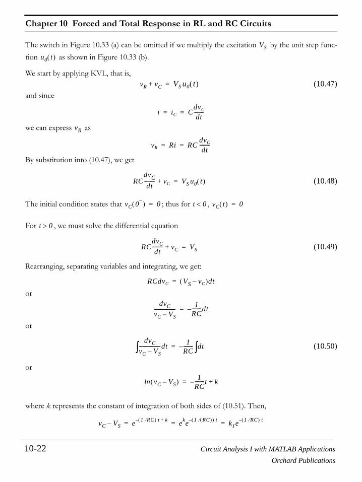
Chapter 10 Forced and Total Response in RL and RC Circuits
10-22 Circuit Analysis I with MATLAB ApplicationsOrchard Publications
The switch in Figure 10.33 (a) can be omitted if we multiply the excitation by the unit step func-tion as shown in Figure 10.33 (b).
We start by applying KVL, that is,(10.47)
and since
we can express as
By substitution into (10.47), we get
(10.48)
The initial condition states that ; thus for , For , we must solve the differential equation
(10.49)
Rearranging, separating variables and integrating, we get:
or
or
(10.50)
or
where k represents the constant of integration of both sides of (10.51). Then,
VS
u0 t( )
vR vC+ VS u0 t( )=
i iC CdvC
dt--------= =
vR
vR Ri RCdvC
dt--------= =
RCdvCdt
--------- vC+ VS u0 t( )=
vC 0−( ) 0= t 0< vC t( ) 0=
t 0>
RCdvCdt
--------- vC+ VS=
RCdvC VS vC–( )dt=
dvCvC VS–----------------- 1
RC--------dt–=
dvCvC VS–-----------------dt∫
1RC-------- dt∫–=
vC VS–( )ln 1RC--------t k+–=
vC VS– e 1 RC⁄( ) t k+– eke 1 RC( )⁄( ) t– k1e 1 RC⁄( ) t–= = =

Circuit Analysis I with MATLAB Applications 10- 23Orchard Publications
The Forced and Total Response in an RC Circuit
or
(10.51)
The constant can be evaluated from the initial condition where by substi-tution into (10.51) we get
or
Therefore, the solution of (10.49) is
(10.52)
As with the circuit of the previous section, we observe that the solution consists of a forcedresponse and a natural response. The constant term is the voltage attained across the capacitor as
and represents the steady-state condition since the capacitor at this state behaves as anopen circuit.
The amplitude of the exponential term natural response is .
The summation of the forced response and the natural response constitutes the total response, i.e.,
or
(10.53)
Now, let us return to the circuit of Figure 10.33 to find the complete (total) response by sum-ming the forced and the natural responses indicated in (10.53).
The forced response is found from the circuit of Figure 10.34 where we let
Figure 10.34. Circuit for derivation of the forced response
Then, from the circuit of Figure 10.34,
vC VS k1e 1 RC⁄( ) t––=
k1 vC 0+( ) vC 0−( ) 0= =
vC 0+( ) 0 VS k1e0–= =
k1 VS=
vC t( ) VS VS e 1 RC⁄( )t––( )u0 t( )=
RLVS
t ∞→ C
VS–
vC t( ) complete response vC t( ) forced response vC t( ) natural response+=
vCtotal vCf vCn+=
RC
vCf t ∞→
+−
R OpenCircuitas t → ∞ VS u0 t( )
vCf
vCf

Chapter 10 Forced and Total Response in RL and RC Circuits
10-24 Circuit Analysis I with MATLAB ApplicationsOrchard Publications
(10.54)
Next, we need to find the natural response and this is found by letting the excitation (forcing func-tion) go to zero as shown in Figure 10.35.
Figure 10.35. Circuit for derivation of the natural response
We found in Chapter 9 that the natural response has the exponential form
and thus the total response is
(10.55)
where the constant is evaluated from the initial condition
Substitution of the initial condition into (10.55) yields
or
With this substitution (10.55) is rewritten as
(10.56)
and this is the same as (10.52).
We can sketch easily if we sketch and separately and then add these. This isdone with Excel and the plots are shown in Figure 10.36.
The time constant is defined as before, and its numerical value can be found from the circuit con-stants and as follows:
vCf VS=
VS u0 t( )
CVS u0 t( ) 0= vCn
R
vCn
vCn
vCn Ae 1 RC⁄( )t–=
vC t( ) vCf vCn+ VS Ae 1 RC⁄( )t–+= =
A vC 0−( ) vC 0( ) vC 0+( ) 0= = =
vC 0+( ) 0 VS Ae0–= =
A VS–=
vC t( ) VS VS e 1 RC⁄( )t––( )u0 t( )=
vCtotal VS VS e 1 RC⁄( )t––
τ
R C
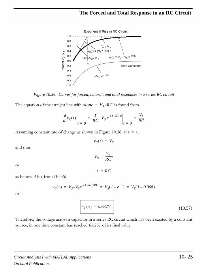
Circuit Analysis I with MATLAB Applications 10- 25Orchard Publications
The Forced and Total Response in an RC Circuit
Figure 10.36. Curves for forced, natural, and total responses in a series RC circuit
The equation of the straight line with is found from
Assuming constant rate of change as shown in Figure 10.36, at ,
and thus
or
as before. Also, from (10.56)
or
(10.57)
Therefore, the voltage across a capacitor in a series RC circuit which has been excited by a constantsource, in one time constant has reached of its final value.
Exponential Rise in RC Circuit
-1.0
-0.8
-0.6
-0.4
-0.2
0.0
0.2
0.4
0.6
0.8
1.0
Per
cent
VC
/ V
STime Constantsτ
vC(t) = (VS / RC) tVC / V S
0.632VC / V S vC(t) = VS − VS e−t / RC
−VS e−t / RC
slope VS RC⁄=
ddt-----vC t( )
t 0=
1RC-------- VS e 1 RC⁄( )t–⋅
t 0=
VSRC--------= =
t τ=
vC t( ) VS=
VSVSRC--------τ=
τ RC=
vC τ( ) VS VS– e 1 RC⁄( )RC– VS 1 e 1––( ) VS 1 0.368–( )= = =
vC τ( ) 0.632VS=
63.2%

Chapter 10 Forced and Total Response in RL and RC Circuits
10-26 Circuit Analysis I with MATLAB ApplicationsOrchard Publications
Example 10.7
For the circuit shown in Figure 10.37 find:
a. and
b. and
c. and
d. for
Figure 10.37. Circuit for Example 10.7
Solution:
a. No initial condition is given so we must assume that sufficient time has elapsed for steady-stateconditions to exist for all We assume time is in seconds since we are not told otherwise.Then, since there is no voltage or current source present to cause current to flow, we get
and
b. Exchanging the current source and the resistor with a voltage source with a series
resistor, the circuit at is as shown in Figure 10. 38.
Figure 10.38. Circuit for Example 10.7 at
vC 1−( ) iC 1−( )
vC 1+( ) iC 1+( )
vC t 10 min.=( ) iC t 10 min.=( )
iC t( ) t 1>
C−+
60 KΩ
10 µF
20 KΩ
10 KΩ
9u0 t 1–( ) mA
vC t( )
iC t( )
t 1 s.<
vC 1−( ) 0=
iC 1−( ) 0=
10 KΩ 10 KΩ
t 1+=
−+
60 KΩ 20 KΩ
10 KΩ+ −iC t( )
C
10 µF
vC t( )
9u0 t 1–( ) V
t 1+=

Circuit Analysis I with MATLAB Applications 10- 27Orchard Publications
The Forced and Total Response in an RC Circuit
Now, since , no current flows through the resistor at ; if it did,the voltage across the capacitor would change instantaneously, and as we know, this is a physicalimpossibility. Instead, the current path is through the capacitor which at exactly acts as a
short circuit since . Therefore,
(10.58)
c. The time is the essentially the same as , and at this time the capacitor voltage is constant and equal to the voltage across the resistor, i.e.,
Also,
d. For
where from part (c)
and
With the voltage source shorted in the circuit of Figure 10.38, the equivalent resistance is
or
Therefore,
(10.59)
We can evaluate the constant using (10.59) where
or
vC 1+( ) vC 1−( )= 60 kΩ t 1+=
t 1+=
vC 1+( ) vC 1−( ) 0= =
iC 1+( ) 90 V20 10+( ) KΩ
---------------------------------- 3 mA= =
t 10 min= t ∞=
vC t 10 min=( ) 60 KΩ
vC t 10 min=( ) vC ∞( )= v60 KΩ90 V
20 10 60+ +( ) KΩ---------------------------------------------- 60 KΩ⋅ 60 V= = =
iC t( ) t ∞=C
dvC
dt-------- 0= =
t 1>iC t( )
t 1>iC f iCn+=
iCf ∞( ) 0=
iCn Ae1 ReqC⁄( ) t–
=
Req 10 KΩ 20 KΩ+( ) || 60 KΩ 20 KΩ= =
ReqC 20 10 3× 10 10 6–×× 0.2 s= =
iCn Ae 1 0.2⁄( ) t– Ae 5t–= =
A
iC 1+( ) 3 mA Ae 5–= =

Chapter 10 Forced and Total Response in RL and RC Circuits
10-28 Circuit Analysis I with MATLAB ApplicationsOrchard Publications
and by substitution into (10.59),
(10.60)
Example 10.8
In the circuit shown in Figure 10.39, the switch is actually an electronic switch and it is open for and closed for . Initially, the capacitor is discharged, i.e., . Compute and
sketch the voltage across the capacitor for two repetitive cycles.
Figure 10.39. Circuit for Example 10.8
Solution:
With the switch in the open position the circuit is as shown in Figure 10.40.
Figure 10.40. Circuit for Example 10.8 with the switch in the open position
For the time period the time constant for the circuit of Figure 10.40 is
Thus, at the end of the first period when the switch is open, the voltage across the capacitor is
(10.61)
Next, with the switch closed for the circuit is as shown in Figure 10.41.
A 3 10 3–×e 5–
-------------------- 0.445= =
iC t( )t 1>
iCf iCn+ iCn 0.445e 5t– u0 t 1–( ) mA= = =
15 µs 15 µs vC 0( ) 0=
+−
VS C
−+
6 V
1 KΩ
350 Ω
250 Ω
0.02 µFvC t( )
+−
VS C
−
+
6 V
1 KΩ 250 Ω
0.02 µFSwitch open
vC t( )
0 topen 15 µs< <
τopen ReqC 1 KΩ 0.25 KΩ+( ) 0.02 10 6–×× 25 µs= = =
vC t( )t 15 µs=
vCf vCn+ VS VS e t RC⁄–– 6 6e 4 104× t–– 6 6e 0.6–– 2.71 V= = = = =
15 tclosed 30 µs< <

Circuit Analysis I with MATLAB Applications 10- 29Orchard Publications
The Forced and Total Response in an RC Circuit
Figure 10.41. Circuit for Example 10.8 with the switch in the closed position
Replacing the circuit to the left of points x and y by its Thevenin equivalent, we get the circuit shownin Figure 10.42.
Figure 10.42. Thevenin equivalent circuit for the circuit of Figure 10.41
The time constant for the circuit of Figure 10.42 where the switch is closed, is
The capacitor voltage for the circuit of Figure 10.42 is
(10.62)
and the constant is evaluated from initial condition at which by (10.62) is
Then,
or
and by substitution into (10.62)
(10.63)
At the end of the first period when the switch is closed, the voltage across the capacitor is
+−
VS C
−+
6 V
1 KΩ350 Ω
250 Ω
0.02 µF
x
ySwitch closed
×
×
vC t( )
+−
VTH C
−+
1.56 V
259 Ω 250 Ω
0.02 µF
RTH VTH3501350------------ 6× 1.56 V= =
RTH350 1000×
1350--------------------------- 259 Ω= =
vC t( )
τclosed ReqC 259 Ω 250 Ω+( ) 0.02 10 6–×× 10.2 µs= = =
vC t( )
vC t( ) vCf vCn+ VTH A1e 1 RC⁄( ) t 15–( )–+ 1.56 A1e 1 10.2⁄( ) t 15–( )–
+= = =
A1 t 15 µs=
vC t( )t 15 µs=
2.71 V=
vC t( )15 t 30< < µs
2.71 1.56 A1e 1 10.2⁄( ) 15 15–( )–+= =
A1 1.15=
vC t( )15 t 30< < µs
1.56 1.15e 1 10.2⁄( ) t 15–( )–+=

Chapter 10 Forced and Total Response in RL and RC Circuits
10-30 Circuit Analysis I with MATLAB ApplicationsOrchard Publications
(10.64)
For the next cycle, that is, for when the switch is open, the time constant is
the same as before, i.e., and the capacitor voltage is
(10.65)
The constant is computed with (10.65) as
or
and by substitution into (10.65)
(10.66)
At the end of the second period when the switch is open, the voltage across the capacitor is
(10.67)
The second period when the switch is closed is Then,
(10.68)
and with (10.67) we get
Therefore,
(10.69)
and
(10.70)
Repeating the above steps for the third open and closed switch periods, we get
(10.71)
vC t( )t 30 µs=
1.56 1.15e 1 10.2⁄( ) 30 15–( )–+ 1.82 V= =
30 topen 45 µs< < τopen
τopen 25 µs=
vC t( ) vCf vCn+ 6 A2e 1 25⁄( ) t 30–( )–+= =
A2
vC t( )t 30 µs=
1.82 6 A2e 1 25⁄( ) 30 30–( )–+= =
A2 4.18–=
vC t( )30 t 45< < µs
6 4.18e 1 25⁄( ) t 30–( )––=
vC t( )t 45 µs=
6 4.18– e 1 25⁄( ) 45 30–( )– 3.71 V= =
45 tclosed 60 µs< <
vC t( )45 t 60< < µs
vCf vCn+ VTH A3e 1 RC⁄( ) t 45–( )–+ 1.56 A3e 1 10.2⁄( ) t 45–( )–+= = =
A3 2.15=
vC t( )45 t 60< < µs
1.56 2.15e 1 10.2⁄( ) t 45–( )–+=
vC t( )t 60 µs=
1.56 2.15e 1 10.2⁄( ) 60 45–( )–+ 2.05 V= =
vC t( )60 t 75< < µs
6 3.95e 1 25⁄( ) t 60–( )––=

Circuit Analysis I with MATLAB Applications 10- 31Orchard Publications
Summary
and
(10.72)
Likewise,
(10.73)
and
(10.74)
and using Excel we get the waveform shown in Figure 10.43.
Figure 10.43. Voltage across the capacitor for the circuit of Example 10.8
10.6 Summary
• The unit step function is defined as
and it is represented by the waveform below.
• Unit step functions can be used to represent other time-varying functions.
• The unit step function offers a convenient method of describing the sudden application of a volt-age or current source.
vC t( )t 75 µs=
3.83 V=
vC t( )75 t 90< < µs
1.56 2.27e 1 10.2⁄( ) t 75–( )–+=
vC t( )t 90 µs=
2.08 V=
0
1
2
3
4
0 15 30 45 60 75 90
Time (µs)
Cap
acito
r Vol
tage
(V)
u0 t( )
u0 t( )0 t 0<1 t 0>⎩
⎨⎧
=
1
0
u0 t( )
Chapter 10 Forced and Total Response in RL and RC Circuits
10-32 Circuit Analysis I with MATLAB ApplicationsOrchard Publications
• The unit ramp function , is defined as the integral of the unit step function, that is,
where τ is a dummy variable. It is also expressed as
• The unit impulse or delta function, denoted as , is the derivative of the unit step . It isdefined as
or
and
• In a simple circuit that is excited by a voltage source the current is
where the forced response represents the steady-state condition reached as . Since theinductor at this state behaves as a short circuit, . The natural response is the sec-
ond term in the parenthesis of the above expression, that is,
• In a simple circuit that is excited by a voltage source the voltage across the capacitoris
where the forced response represents the steady-state condition reached as . Since the
capacitor at this state behaves as an open circuit, . The natural response is the
second term in the parenthesis of the above expression, that is, . The constant must be evaluated from the total response.
u1 t( )
u1 t( ) u0 τ( ) τd∞–
t
∫=
u1 t( )0 t 0<t t 0≥⎩
⎨⎧
=
δ t( ) u0 t( )
δ τ( ) ddt-----u0 t( )=
δ τ( ) τd∞–
t
∫ u0 t( )=
δ t( ) 0 for all t 0≠=
RL VS u0 t( )
i t( ) if in+VSR------
VSR------e R L⁄( ) t–
–⎝ ⎠⎛ ⎞ u0 t( )= =
if t ∞→
L if VS R⁄= in
in VS R⁄–( )e R L⁄( ) t–=
RC VS u0 t( )
vC t( ) vCf vCn+ VS Ae 1 RC⁄( )t–+( )u0 t( )= =
vCf t ∞→
C vCf VS= vCn
vCn Ae 1 RC⁄( )t–= A
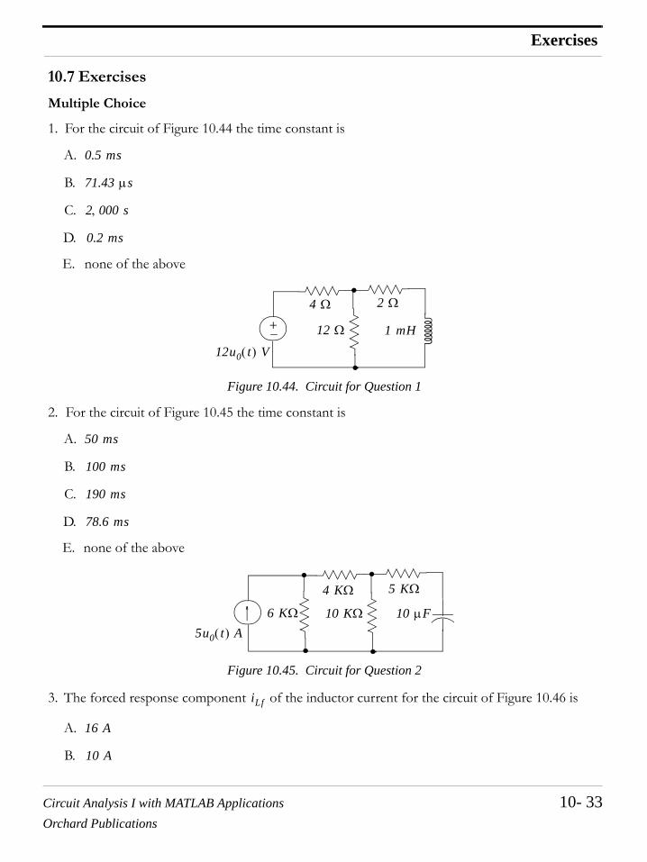
Circuit Analysis I with MATLAB Applications 10- 33Orchard Publications
Exercises
10.7 Exercises
Multiple Choice
1. For the circuit of Figure 10.44 the time constant is
A.
B.
C.
D.
E. none of the above
Figure 10.44. Circuit for Question 1
2. For the circuit of Figure 10.45 the time constant is
A.
B.
C.
D.
E. none of the above
Figure 10.45. Circuit for Question 2
3. The forced response component of the inductor current for the circuit of Figure 10.46 is
A.
B.
0.5 ms
71.43 µs
2 000 s,
0.2 ms
+−12u0 t( ) V
4 Ω
12 Ω
2 Ω
1 mH
50 ms
100 ms
190 ms
78.6 ms
5u0 t( ) A10 µF6 KΩ
4 KΩ
10 KΩ
5 KΩ
iLf
16 A
10 A
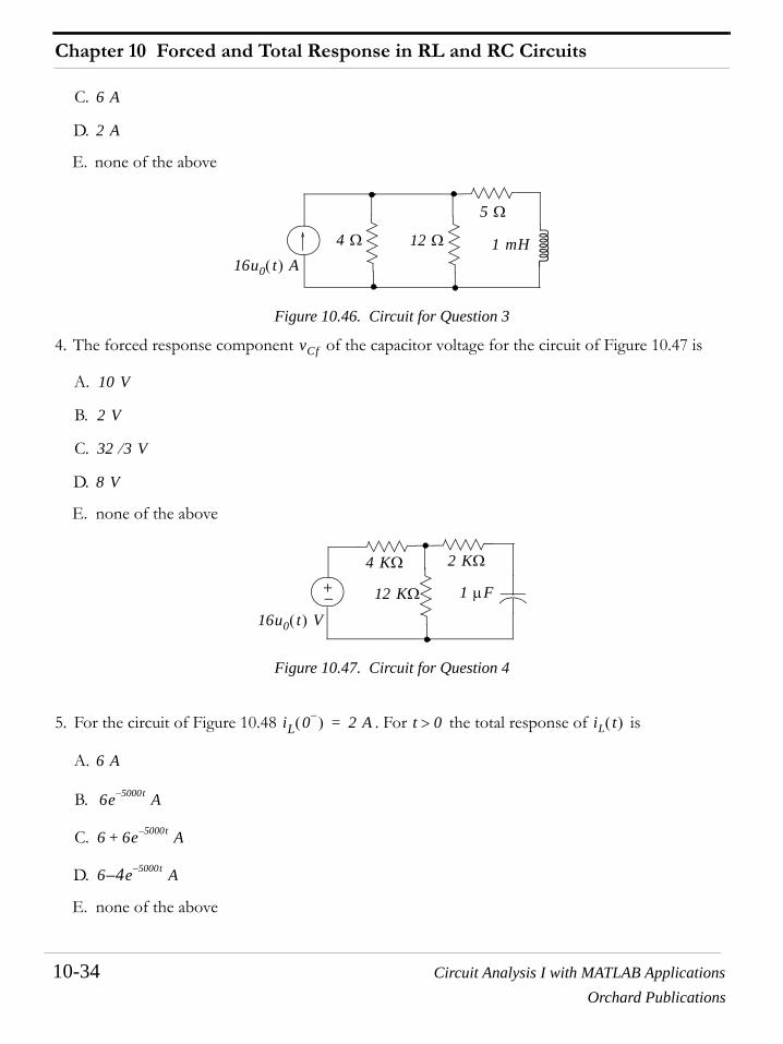
Chapter 10 Forced and Total Response in RL and RC Circuits
10-34 Circuit Analysis I with MATLAB ApplicationsOrchard Publications
C.
D.
E. none of the above
Figure 10.46. Circuit for Question 3
4. The forced response component of the capacitor voltage for the circuit of Figure 10.47 is
A.
B.
C.
D.
E. none of the above
Figure 10.47. Circuit for Question 4
5. For the circuit of Figure 10.48 . For the total response of is
A.
B.
C.
D.
E. none of the above
6 A
2 A
16u0 t( ) A4 Ω 12 Ω
5 Ω
1 mH
vCf
10 V
2 V
32 3⁄ V
8 V
+−16u0 t( ) V
4 KΩ
12 KΩ
2 KΩ
1 µF
iL 0−( ) 2 A= t 0> iL t( )
6 A
6e 5000t– A
6 6e 5000t– A+
6 4– e 5000t– A
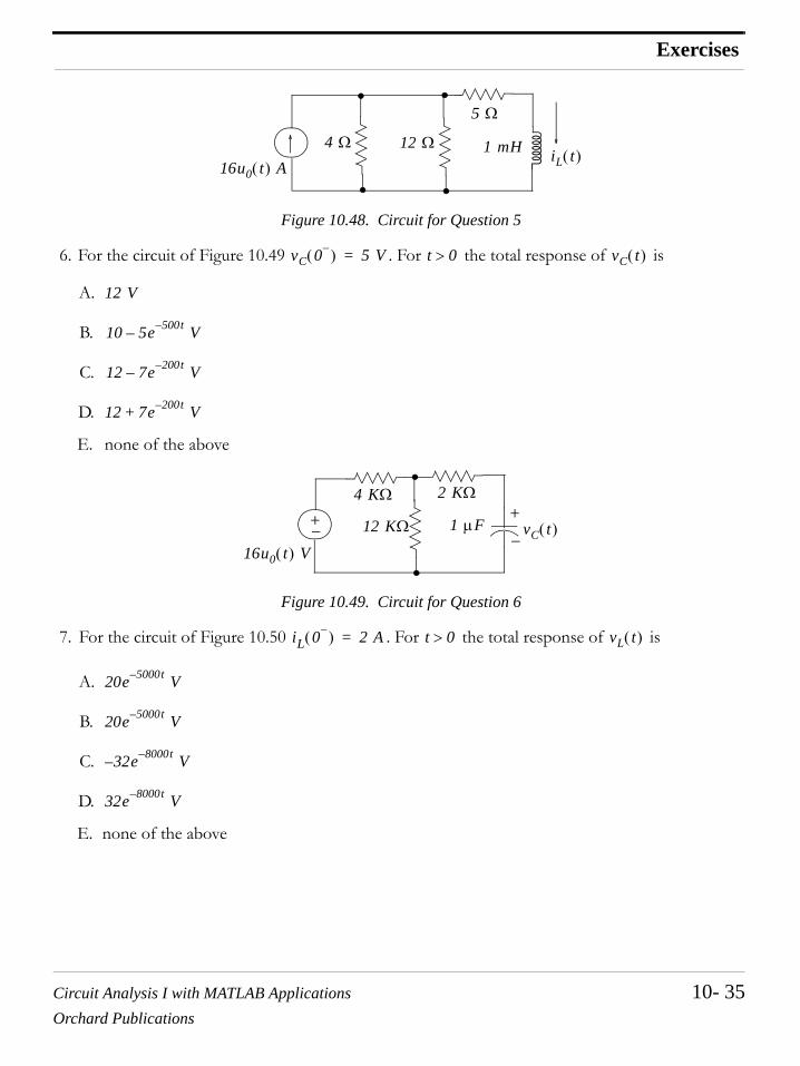
Circuit Analysis I with MATLAB Applications 10- 35Orchard Publications
Exercises
Figure 10.48. Circuit for Question 5
6. For the circuit of Figure 10.49 . For the total response of is
A.
B.
C.
D.
E. none of the above
Figure 10.49. Circuit for Question 6
7. For the circuit of Figure 10.50 . For the total response of is
A.
B.
C.
D.
E. none of the above
16u0 t( ) A4 Ω 12 Ω
5 Ω
1 mH iL t( )
vC 0−( ) 5 V= t 0> vC t( )
12 V
10 5e 500t– V–
12 7e 200t– V–
12 7e 200t– V+
+−16u0 t( ) V
4 KΩ
12 KΩ
2 KΩ
1 µF+
−vC t( )
iL 0−( ) 2 A= t 0> vL t( )
20e 5000t– V
20e 5000t– V
32e 8000t– V–
32e 8000t– V

Chapter 10 Forced and Total Response in RL and RC Circuits
10-36 Circuit Analysis I with MATLAB ApplicationsOrchard Publications
Figure 10.50. Circuit for Question 7
8. For the circuit of Figure 10.51 . For the total response is
A.
B.
C.
D.
E. none of the above
Figure 10.51. Circuit for Question 8
9. The waveform of Figure 10.52 can be expressed as
A.
B.
C.
D.
E. none of the above
16u0 t( ) A4 Ω 12 Ω
5 Ω
1 mH vL t( )+
−
vC 0−( ) 5 V= t 0> iC t( )
1400e 200t– A
1.4e 200t– A
3500e 500t– A
3.5e 500t– A
+−16u0 t( ) V
4 KΩ
12 KΩ
2 KΩ
1 µF iC t( )
3tu0 t( ) A
3 u0 t( )[ ] 3 u0 t 3–( )[ ] A–
3t u0 t( ) u0 t 1–( )–[ ] 1.5t– 4.5+( ) u0 t 1–( ) u0 t 3–( )–[ ] A+
3t u0 t( ) u0 t 3–( )–[ ] 1.5t– 4.5+( ) u0 t( ) u0 t 3–( )–[ ] A+

Circuit Analysis I with MATLAB Applications 10- 37Orchard Publications
Exercises
Figure 10.52. Waveform for Question 9
10. The waveform of Figure 10.53 can be expressed as
A.
B.
C.
D.
E. none of the above
Figure 10.53. Waveform for Question 10
Problems
1. In the circuit of Figure 10.54, the voltage source varies with time as shown by the wave-form of Figure 10.55. Compute, sketch, and express as a sum of unit step functions for
iL t( ) A
t s( )
1
1 2
2
3
3
2 1 e αt–– e β t––( )u0 t( ) V
2 2e α t––( ) u0 t( ) u0 t 2–( )–[ ] 2e β t–( ) u0 t 2–( ) u0 t 3–( )–[ ] V+
2 2e αt––( ) u0 t( ) u0 t 2–( )–[ ] 2e β t–( )– u0 t 2–( ) u0 t 3–( )–[ ] V
2 2e αt––( ) u0 t( )[ ] 2e βt–( )– u0 t 3–( )[ ] V
vC t( ) V
t s( )
1
1 2
2
3
2 2e α t––
2e βt–
vS t( )
vLOAD t( )
0 t 5 s.≤ ≤
Chapter 10 Forced and Total Response in RL and RC Circuits
10-38 Circuit Analysis I with MATLAB ApplicationsOrchard Publications
Figure 10.54. Circuit for Problem 1
Figure 10.55. Waveform for Problem 1
2. In the circuit of Figure 10.56, . Compute for .
Figure 10.56. Circuit for Problem 2
3. In the circuit of Figure 10.57 (a), the excitation is a pulse as shown in Figure 10.57 (b).
a. Compute for
b. Compute and sketch for all
+
−12 Ω
6 Ω 6 Ω
10 Ω
+vLOAD t( )
vS t( )−
0
60
120
−60
1 2 3 4 5 6
(V)
t(s)
vS t( )
vS t( ) 15u0 t( ) 30u0 t 2–( ) V–= iL t( ) t 0>
+−
R
L3 KΩ
1 mH
iL t( )vS t( )
vS t( )
iL t( ) 0 t 0.3 ms< <
iL t( ) t 0>

Circuit Analysis I with MATLAB Applications 10- 39Orchard Publications
Exercises
Figure 10.57. Circuit and waveform for Problem 3
4. In the circuit of Figure 10.58, switch has been open for a very long time and closes at .Compute and sketch and for .
Figure 10.58. Circuit for Problem 4
5. For the circuit of Figure 10.59, compute for .
Figure 10.59. Circuit for Problem 5
6. For the circuit of Figure 10.60, compute for in terms of , , and given
that
+− 6 Ω
3 Ω 1 mH 24
t (ms)0.3
6 Ω
(a) (b)
iL t( )
vS t( )
vS t( ) V
S t 0=
iL t( ) iSW t( ) t 0>
+−
6 Ω4 Ω
1 H8 Ω20 V
St 0=vS
iSW t( )
iL t( )
vC t( ) t 0>
−+
38 Ω
50 µF2 Ω+
−24 V
vS
vC t( )
10u0 t( ) A
vout t( ) t 0> R C vinu0 t( )
vC 0−( ) 0=

Chapter 10 Forced and Total Response in RL and RC Circuits
10-40 Circuit Analysis I with MATLAB ApplicationsOrchard Publications
Figure 10.60. Circuit for Problem 6
7. In the circuit of Figure 10.61, switch S has been open for a very long time and closes at .Compute and sketch and for .
Figure 10.61. Circuit for Problem 7
8. For the circuit of Figure 10.62, it is given that . Compute for . Hint: Becareful in deriving the time constant for this circuit.
Figure 10.62. Circuit for Problem 8
R
C
vinu0 t( )vout t( )
t 0=
vC t( ) vR3 t( ) t 0>
+−
C25 KΩ50 KΩ
1 µF
100 KΩ
R1 R2
R3
+−
−
++
−S
50 V
t 0=
vC t( )
vR3 t( )
vS1
vS2
100u0 t–( ) V
vC 0−( ) 5 V= iC t( ) t 0>
C18 Ω
1 F
R1 R2
−
+
+−
12 ΩvC t( )
iC t( )
10iC t( )

Circuit Analysis I with MATLAB Applications 10- 41Orchard Publications
Answers to Exercises
10.8 Answers to Exercises
Multiple Choice
1. D
2. B
3. C
4. E
5. E
6. C
7. D
8. A
9. C
10. B
Problems
1. We replace the given circuit shown below with its Thevenin equivalent.
For the Thevenin equivalent voltage at different time intervals is as shown below.
12 V
6 4e 8000t– A–
+
−12 Ω
6 Ω 6 Ω
10 Ω
+vLOAD t( )
vS t( )×
×
y
x
+
−10 Ω
10 Ω +
vLOAD t( )
vTH t( )−−
0
60
120
−60
1 2 3 4 5 6
(V)
t(s)
vS t( )

Chapter 10 Forced and Total Response in RL and RC Circuits
10-42 Circuit Analysis I with MATLAB ApplicationsOrchard Publications
and
The waveform of the voltage across the load is as shown below.
The waveform above can now be expressed as a sum of unit step functions as follows:
2. The circuit at is as shown below and since we are not told otherwise, we will assume that
For we let be the inductor current when the voltage source acts alone and when the voltage source acts alone. Then,
vTH t( )
1218------vs t( ) 2
3--- 60× 40 V 0 t 1 s< <= =
1218------vs t( ) 2
3--- 120× 80 V 1 t 3 s< <= =
1218------vs t( ) 2
3--- 60–( )× 40– V 3 t 4 s< <= =
1218------vs t( ) 2
3--- 60× 40 V t 4> s= =⎝
⎜⎜⎜⎜⎜⎜⎜⎜⎜⎛
=
vLOAD t( ) 1020------vTH t( ) 0.5vTH t( )
0.5 40× 20 V 0 t 1 s< <=
0.5 80× 40 V 1 t 3 s< <=
0.5 40–( )× 20– V 3 t 4 s< <=
0.5 40× 20 V t 4> s=⎝⎜⎜⎜⎜⎛
= = =
vLOAD t( ) V( )
40
20
0
20–
t s( )1 2 3 4 5
vLOAD t( ) 20u0 t( ) 20u0 t 1–( )– 40u0 t 1–( ) 40u0 t 3–( )– 20u0 t 4–( )+ +=
20u0 t 3–( ) 20u0 t 4–( ) 20u0 t 4–( )+ +–
20u0 t( ) 20u0 t 1–( ) 60u0 t 3–( )– 40u0 t 4–( )+ +=
t 0−=
iL 0−( ) 0=
t 0> iL1 t( ) 15u0 t( )
iL2 t( ) 30u0 t 2–( ) iL TOTAL t( ) iL1 t( ) iL2 t( )+=

Circuit Analysis I with MATLAB Applications 10- 43Orchard Publications
Answers to Exercises
For the circuit is as shown below.
Then, where and
Thus, and using the initial condition , we get
or . Therefore,
(1)
Next, with the voltage source acts alone the circuit is as shown below.
Then, , and
Thus, and the initial condition at is found from (1)
above as . Therefore,
or and
(2)
3 kΩ1 mH
iL 0−( ) 0=vS 0−( ) 0=
0 t 2 s< <
+−
3 KΩ
1 mH
iL1 t( )
15 V
iL1 t( ) iL1f iL1n+= iL1f15
3 KΩ-------------- 5 mA= = iL1n A1e R L⁄( ) t– Ae 3 106t×–= =
iL1 t( ) 5 A1e 3 106t×– mA+= iL 0−( ) iL 0+( ) 0= =
iL1 0( ) 5 A1e0 mA+= A1 5–=
iL1 t( ) 5 5e 3 106t×––=
30u0 t 2–( )
+−
3 KΩ
1 mH
iL t( )30 V
iL2 t( ) iL2f iL2n+= iL2f30–
3 KΩ-------------- 10– mA= = iL2n A2e R L⁄( ) t 2–( )– Be 3 106 t 2–( )×–= =
iL2 t( ) 10– A2e 3 106 t 2–( )×– mA+= t 2=
iL1 t 2 s=5 5e 6 106t×–– 5 mA≈=
iL2 t 2 s=iL1 t 2 s=
5 10– A2e 3 106 2 2–( )×– mA+= = = A2 15=
iL2 t( ) 10– 15e 3 106 t 2–( )×– mA+=

Chapter 10 Forced and Total Response in RL and RC Circuits
10-44 Circuit Analysis I with MATLAB ApplicationsOrchard Publications
Therefore, the total current when both voltage sources are present is the summation of (1) and(2), that is,
3.a. For this circuit and since we are not told otherwise, we will
assume that . For the circuit and its Thevenin equivalent are asshown below.
Then,
and at
or and thus for
(1)
b. For the circuit is as shown below. For this circuit
(2)
and is found from the initial condition at , that is, with (1) above we get
iL TOTAL t( ) iL1 t( ) iL2 t( )+ 5 5e 3 106t×–– 10– 15e 3 106 t 2–( )×– mA+= =
5 5e 3 106t×––– 15e 3 106 t 2–( )×– mA+=
vS t( ) 24 u0 t( ) u0 t 0.3–( )–[ ]=
iL 0−( ) 0= 0 t 0.3 ms< <
+−
6 Ω3 Ω
1 mH6 Ω iL t( )
vS t( ) 24 u0 t( ) u0 t 0.3–( )–[ ]=×
×
+−
8 Ω
1 mH iL t( )
vTH t( )
vTH t( ) 16 u0 t( ) u0 t 0.3–( )–[ ]=
vS t( )
iL t( ) iLf iLn+ 16 8⁄ A1e R L⁄( ) t–+ 2 Ae 8000t–+= = =
t 0=
iL 0( ) iL 0−( ) 0 2 A1e0+= = =
A1 2–= 0 t 0.3 ms< <
iL t( ) 2 2– e 8000t–=
t 0.3 ms>
iL t( ) A2e R L⁄( ) t 0.3–( )– A2e 8000 t 0.3–( )–= =
A2 t 0.3 ms=
6 Ω3 Ω
1 mH6 Ω iL t( )
×
×
8 Ω 1 mH iL t( )vS t( ) 0=

Circuit Analysis I with MATLAB Applications 10- 45Orchard Publications
Answers to Exercises
and by substitution into (2) above
or . Therefore for
The waveform for the inductor current for all is shown below.
4. At the circuit is as shown below where and thus the initialcondition has been established.
For the circuit and its Thevenin equivalent are as shown below where
and
iL t 0.3 ms=2 2e 8 103 0.3 10 3–×××–– 2 2e2.4– 1.82 A= = =
iL t 0.3 ms=1.82 A2e 8000 0.3 0.3–( )–= =
A2 1.82= t 0.3 ms>
iL t( ) 1.82e t 0.3 ms–( )–=
iL t( ) t 0>
t ms( )
iL A( )
1.82
0.3
t 0−= iL 0−( ) 20 4 6+( )⁄ 2 A= =
+−
6 Ω4 Ω
20 V
vS
iL 0−( )
t 0>
vTH8
4 8+------------ 20× 40 3⁄ V= =
RTH8 4×8 4+------------ 6+ 26 3⁄ Ω= =
Chapter 10 Forced and Total Response in RL and RC Circuits
10-46 Circuit Analysis I with MATLAB ApplicationsOrchard Publications
Then,
and is evaluated from the initial condition, i.e.,
from which and thus for
(1)
Next, to find we observe that this current flows also through the resistor and this canbe found from shown on the circuit below.
Now,
and
+−
6 Ω
4 Ω
1 H8 Ω20 V
vS
iL t( )
ClosedSwitch
+− 1 H
vTH
iL t( )
40 3⁄ V
26 3⁄ ΩRTH
iL t( ) iLf iLn+ 40 3⁄26 3⁄------------- Ae R L⁄( )t–+ 20 13⁄ Ae 26 3⁄( )t–+= = =
A
iL 0−( ) iL 0+( ) 2 20 13⁄ Ae0+= = =
A 6 13⁄= t 0>
iL t( ) 2013------ 6
13------e 26 3⁄( )t–+ 1.54 0.46e 8.67t–+= =
iSW t( ) 8 Ω
v8 Ω
+−
6 Ω
4 Ω
1 H8 Ω20 V
vS
iL t( )
+
−
iSW t( )
v8 Ω
v8 Ω v6 Ω vL t( )+ 6iL t( ) LdiLdt-------+= =
6 1.54 0.46e 8.67t–+( ) 1 ddt----- 1.54 0.46e 8.67t–+( )×+=
9.24 2.76e 8.67t– 8.67 0.46e 8.67t–×–+=
9.24 1.23e 8.67t––=

Circuit Analysis I with MATLAB Applications 10- 47Orchard Publications
Answers to Exercises
(2)
Therefore, from the initial condition, (1) and (2) above we have
and with these values we sketch and as shown below.
5. At the circuit is as shown below where and thus the initial condition hasbeen established.
The circuit for is shown below where the current source has been replaced with a voltagesource.
Now,
iSW t( ) i8 Ωv8 Ω
8---------- 9.24 1.23e 8.67t––
8----------------------------------------- 1.16 0.15e 8.67t––= = = =
iL 0+( ) 2= iL ∞( ) 1.54= iSW 0+( ) 1.16 0.15– 1.01= = iSW ∞( ) 1.16=
iL t( ) iSW t( )
iL t( ) A iSW t( ) A
tt
0.5
2.0
1.5
1.01.01
1.16
t 0−= vC 0−( ) 24 V=
−+
38 Ω
50 µF
2 Ω
+−
24 V
vS
vC t( )
t 0>
−+
38 Ω
50 µF
2 Ω+−
24 V
vS
vC t( )
+ −
20 V
−
+40 Ω
50 µF
+−
4 V
vC t( )
vC t( ) vCf vCn+ 4 Ae 1 RC( )⁄ t–+ 4 Ae 500t–+= = =

Chapter 10 Forced and Total Response in RL and RC Circuits
10-48 Circuit Analysis I with MATLAB ApplicationsOrchard Publications
and with the initial condition from which we get
6. For the op amp circuit is as shown below.
Application of KCL at the minus (−) input yields
and since
or
Integrating both sides and observing that we get
where is the constant of integration of both sides and it is evaluated from the given initial condi-tion. Then,
or . Therefore,
and is the slope as shown below.
vC 0−( ) vC 0+( ) 24 V 4 Ae0+= = = A 20=
vC t( ) 4 20e 500t–+=
t 0>
R
C
vin t( )vout t( )
+ +−
−
v−
+ −
v− vin–
R------------------- C
dvCdt
---------+ 0=
v− 0=
CdvCdt
---------vinR
-------=
dvCdt
---------vinRC--------=
vout t( ) vC t( )–=
vout t( )vinRC--------t– k+=
k
vC 0−( ) vC 0+( ) 0 0 k+= = =
k 0=
vout t( )vinRC-------- t⎝ ⎠
⎛ ⎞– u0 t( )=
vin RC⁄

Circuit Analysis I with MATLAB Applications 10- 49Orchard Publications
Answers to Exercises
7. At the circuit is as shown below where and thus the initial condition hasbeen established.
The circuit for is shown below where the voltage source is absent for all positive timeand the is shorted out by the closed switch.
For the circuit above
and with the initial condition
from which and thus for
To find we will first find from the circuit below where
slope vin RC⁄–=
t 0−= vC 0−( ) 150 V=
+−
175 KΩ
1 µF150 V+
vC 0−( )−
t 0> vS1
50 KΩ
+−
125 KΩ
1 µF50 V
+
vC t( )−
vC t( ) vCf vCn+ 50 Ae t RC( )⁄–+ 50 Ae 8t–+= = =
vC 0−( ) vC 0+( ) 150 50 Ae0+= = =
A 100= t 0>
vC t( ) 50 100e 8t– V+=
vR3 t( ) iC t( )
iC t( ) CdvCdt
--------- 10 6– 8 10 4– e 8t–×–( )×= =
Chapter 10 Forced and Total Response in RL and RC Circuits
10-50 Circuit Analysis I with MATLAB ApplicationsOrchard Publications
Then,
The sketches below show and as they approach their final values.
8. For this circuit we cannot short the dependent source and therefore we cannot find by com-bining the resistances and in parallel combination in order to find the time constant
. Instead, we will derive the time constant from the differential equation of (9.9) of theprevious chapter, that is,
From the given circuit shown below
or
+−
25 KΩ1 µF
100 KΩ50 V−
++
−vC t( )
vR3 t( )
vR3 t( ) 100 KΩ( )iC 105 8 10 4– e 8t–×–( ) 80e 8t– V–= = =
vC t( ) vR3 t( )
150
100
50 80–
0
0
vR3 t( ) VvC t( ) V
t
t
Req
R1 R2
τ RC=
dvCdt
---------vCRC--------+ 0=
C18 Ω
1 F
R1 R2
−
+
+−
12 ΩvC t( )
iC t( )
10iC t( )
vC
iCvC 10iC–
R1----------------------
vCR2------+ +

Circuit Analysis I with MATLAB Applications 10- 51Orchard Publications
Answers to Exercises
or
or
and from this differential equation we see that the coefficient of is
and thus
and with the given initial condition we get
Then, using
we find that for
and the minus (−) sign indicates that the direction is opposite to that shown.
CdvCdt
--------- 1R1------ 1
R2------+⎝ ⎠
⎛ ⎞ vC10R1------C
dvCdt
---------–+ 0=
1 10R1------–⎝ ⎠
⎛ ⎞ CdvCdt
---------⎝ ⎠⎛ ⎞ R1 R2+
R1 R2⋅------------------⎝ ⎠
⎛ ⎞ vC+ 0=
dvCdt
---------
R1 R2+
R1 R2⋅------------------⎝ ⎠
⎛ ⎞
1 10R1------–⎝ ⎠
⎛ ⎞ C⋅------------------------------vC+ 0=
vC
1ReqC------------ 1
τ--- 30 216⁄
1 1018------–⎝ ⎠
⎛ ⎞ 1⋅----------------------------- 30 216⁄
8 18⁄------------------- 15 9×
4 108×------------------ 135
432--------- 5
16------ 0.3125= = = = = = =
vC t( ) Ae 0.3125t–=
vC 0−( ) V0 A 5 V= = =
vC t( ) 5e 0.3125t–=
iC CdvCdt
---------=
t 0>
iC t( ) 1( ) 0.3125 5e 0.3125t–×–( ) 1.5625e 0.3125t––= =
iC t( )

Chapter 10 Forced and Total Response in RL and RC Circuits
10-52 Circuit Analysis I with MATLAB ApplicationsOrchard Publications
NOTES

Circuit Analysis I with MATLAB Applications A-1Orchard Publications
Appendix AIntroduction to MATLAB®
his appendix serves as an introduction to the basic MATLAB commands and functions, proce-dures for naming and saving the user generated files, comment lines, access to MATLAB’s Edi-tor/Debugger, finding the roots of a polynomial, and making plots. Several examples are pro-
vided with detailed explanations.
A.1 MATLAB® and Simulink®
MATLAB and Simulink are products of The MathWorks, Inc. These are two outstanding softwarepackages for scientific and engineering computations and are used in educational institutions and inindustries including automotive, aerospace, electronics, telecommunications, and environmentalapplications. MATLAB enables us to solve many advanced numerical problems fast and efficiently.Simulink is a block diagram tool used for modeling and simulating dynamic systems such as controls,signal processing, and communications. In this appendix we will discuss MATLAB only.
A.2 Command Window
To distinguish the screen displays from the user commands, important terms, and MATLAB func-tions, we will use the following conventions:
Click: Click the left button of the mouse
Courier Font: Screen displays
Helvetica Font: User inputs at MATLAB’s command window prompt >> or EDU>>*
Helvetica Bold: MATLAB functions
Times Bold Italic: Important terms and facts, notes and file names
When we first start MATLAB, we see the toolbar on top of the command screen and the promptEDU>>. This prompt is displayed also after execution of a command; MATLAB now waits for a newcommand from the user. It is highly recommended that we use the Editor/Debugger to write our pro-gram, save it, and return to the command screen to execute the program as explained below.
To use the Editor/Debugger:
1. From the File menu on the toolbar, we choose New and click on M-File. This takes us to the Editor
* EDU>> is the MATLAB prompt in the Student Version
T

Appendix A Introduction to MATLAB®
A-2 Circuit Analysis I with MATLAB ApplicationsOrchard Publications
Window where we can type our code (list of statements) for a new file, or open a previously savedfile. We must save our program with a file name which starts with a letter. Important! MATLAB iscase sensitive, that is, it distinguishes between upper- and lower-case letters. Thus, t and T are two dif-ferent letters in MATLAB language. The files that we create are saved with the file name we useand the extension .m; for example, myfile01.m. It is a good practice to save the code in a filename that is descriptive of our code content. For instance, if the code performs some matrix oper-ations, we ought to name and save that file as matrices01.m or any other similar name. We shouldalso use a floppy disk to backup our files.
2. Once the code is written and saved as an m-file, we may exit the Editor/Debugger window by clickingon Exit Editor/Debugger of the File menu. MATLAB then returns to the command window.
3. To execute a program, we type the file name without the .m extension at the >> prompt; then, wepress <enter> and observe the execution and the values obtained from it. If we have saved our filein drive a or any other drive, we must make sure that it is added it to the desired directory in MAT-LAB’s search path. The MATLAB User’s Guide provides more information on this topic.
Henceforth, it will be understood that each input command is typed after the >> prompt and fol-lowed by the <enter> key.
The command help matlab\iofun will display input/output information. To get help with otherMATLAB topics, we can type help followed by any topic from the displayed menu. For example, toget information on graphics, we type help matlab\graphics. The MATLAB User’s Guide containsnumerous help topics.
To appreciate MATLAB’s capabilities, we type demo and we see the MATLAB Demos menu. Wecan do this periodically to become familiar with them. Whenever we want to return to the commandwindow, we click on the Close button.
When we are done and want to leave MATLAB, we type quit or exit. But if we want to clear all pre-vious values, variables, and equations without exiting, we should use the command clear. This com-mand erases everything; it is like exiting MATLAB and starting it again. The command clc clears thescreen but MATLAB still remembers all values, variables and equations that we have already used. Inother words, if we want to clear all previously entered commands, leaving only the >> prompt on theupper left of the screen, we use the clc command.
All text after the % (percent) symbol is interpreted as a comment line by MATLAB, and thus it isignored during the execution of a program. A comment can be typed on the same line as the functionor command or as a separate line. For instance,
conv(p,q) % performs multiplication of polynomials p and q.
% The next statement performs partial fraction expansion of p(x) / q(x)
are both correct.

Circuit Analysis I with MATLAB Applications A-3Orchard Publications
Roots of Polynomials
One of the most powerful features of MATLAB is the ability to do computations involving complexnumbers. We can use either , or to denote the imaginary part of a complex number, such as 3-4ior 3-4j. For example, the statement
z=3−4j
displays
z = 3.0000-4.0000i
In the above example, a multiplication (*) sign between 4 and was not necessary because the com-plex number consists of numerical constants. However, if the imaginary part is a function, or variablesuch as , we must use the multiplication sign, that is, we must type cos(x)*j or j*cos(x) for theimaginary part of the complex number.
A.3 Roots of Polynomials
In MATLAB, a polynomial is expressed as a row vector of the form . Theseare the coefficients of the polynomial in descending order. We must include terms whose coeffi-cients are zero.
We find the roots of any polynomial with the roots(p) function; p is a row vector containing thepolynomial coefficients in descending order.
Example A.1
Find the roots of the polynomial
Solution:
The roots are found with the following two statements where we have denoted the polynomial as p1,and the roots as roots_ p1.
p1=[1 −10 35 −50 24] % Specify and display the coefficients of p1(x)
p1 =
1 -10 35 -50 24
roots_ p1=roots(p1) % Find the roots of p1(x)
roots_p1 =
4.0000
3.0000
i j
j
x( )cos
an an 1– … a2 a1 a0[ ]
p1 x( ) x4
10x3
– 35x2
50x– 24+ +=

Appendix A Introduction to MATLAB®
A-4 Circuit Analysis I with MATLAB ApplicationsOrchard Publications
2.0000
1.0000
We observe that MATLAB displays the polynomial coefficients as a row vector, and the roots as acolumn vector.
Example A.2
Find the roots of the polynomial
Solution:
There is no cube term; therefore, we must enter zero as its coefficient. The roots are found with thestatements below, where we have defined the polynomial as p2, and the roots of this polynomial asroots_ p2. The result indicates that this polynomial has three real roots, and two complex roots. Ofcourse, complex roots always occur in complex conjugate* pairs.
p2=[1 −7 0 16 25 52]
p2 =
1 -7 0 16 25 52
roots_ p2=roots(p2)
roots_ p2 =
6.5014
2.7428
-1.5711
-0.3366+ 1.3202i
-0.3366- 1.3202i
A.4 Polynomial Construction from Known Roots
We can compute the coefficients of a polynomial, from a given set of roots, with the poly(r) functionwhere r is a row vector containing the roots.
* By definition, the conjugate of a complex number is
p2 x( ) x5
7x4
– 16x2
25x+ + 52+=
A a jb+= A∗ a jb–=

Circuit Analysis I with MATLAB Applications A-5Orchard Publications
Polynomial Construction from Known Roots
Example A.3
It is known that the roots of a polynomial are . Compute the coefficients of this poly-nomial.
Solution:
We first define a row vector, say , with the given roots as elements of this vector; then, we find thecoefficients with the poly(r) function as shown below.
r3=[1 2 3 4] % Specify the roots of the polynomial
r3 =
1 2 3 4
poly_r3=poly(r3) % Find the polynomial coefficients
poly_r3 =
1 -10 35 -50 24
We observe that these are the coefficients of the polynomial of Example A.1.
Example A.4
It is known that the roots of a polynomial are . Find the coefficientsof this polynomial.
Solution:
We form a row vector, say , with the given roots, and we find the polynomial coefficients with thepoly(r) function as shown below.
r4=[ −1 −2 −3 −4+5j −4−5j ]
r4 =
Columns 1 through 4
-1.0000 -2.0000 -3.0000 -4.0000+ 5.0000i
Column 5
-4.0000- 5.0000i
poly_r4=poly(r4)
poly_r4 =
1 14 100 340 499 246
1 2 3 and 4, , ,
r3
p1 x( )
1 2 3 4 j5 and 4 j5–+,–,–,–
r4

Appendix A Introduction to MATLAB®
A-6 Circuit Analysis I with MATLAB ApplicationsOrchard Publications
Therefore, the polynomial is
A.5 Evaluation of a Polynomial at Specified Values
The polyval(p,x) function evaluates a polynomial at some specified value of the independentvariable x.
Example A.5
Evaluate the polynomial
(A.1)
at .
Solution:
p5=[1 −3 0 5 −4 3 2]; % These are the coefficients
% The semicolon (;) after the right bracket suppresses the display of the row vector
% that contains the coefficients of p5.
%
val_minus3=polyval(p5, −3) % Evaluate p5 at x=−3; no semicolon is used here
% because we want the answer to be displayed
val_minus3 =
1280
Other MATLAB functions used with polynomials are the following:
conv(a,b) − multiplies two polynomials a and b
[q,r]=deconv(c,d) −divides polynomial c by polynomial d and displays the quotient q and remain-der r.
polyder(p) − produces the coefficients of the derivative of a polynomial p.
Example A.6
Let
and
p4 x( ) x5
14x4
100x3
340x2
499x 246+ + + + +=
p x( )
p5 x( ) x6 3x5– 5x3 4x2
– 3x 2+ + +=x 3–=
p1 x5 3x4– 5x2 7x 9+ + +=

Circuit Analysis I with MATLAB Applications A-7Orchard Publications
Evaluation of a Polynomial at Specified Values
Compute the product using the conv(a,b) function.
Solution:
p1=[1 −3 0 5 7 9]; % The coefficients of p1
p2=[2 0 −8 0 4 10 12]; % The coefficients of p2
p1p2=conv(p1,p2) % Multiply p1 by p2 to compute coefficients of the product p1p2
p1p2 =
2 -6 -8 34 18 -24 -74 -88 78 166 174 108
Therefore,
Example A.7
Let
and
Compute the quotient using the [q,r]=deconv(c,d) function.
Solution:
% It is permissible to write two or more statements in one line separated by semicolons
p3=[1 0 −3 0 5 7 9]; p4=[2 −8 0 0 4 10 12]; [q,r]=deconv(p3,p4)
q =
0.5000
r =
0 4 -3 0 3 2 3
p2 2x6 8x4– 4x2 10x 12+ + +=
p1 p2⋅
p1 p2⋅ 2x11 6x10 8x9–– 34x8 18x7 24x6
–+ +=
74x5 88x4 78x3 166x2 174x 108+ + + +––
p3 x7 3x5– 5x3 7x 9+ + +=
p4 2x6 8x5– 4x2 10x 12+ + +=
p3 p4⁄

Appendix A Introduction to MATLAB®
A-8 Circuit Analysis I with MATLAB ApplicationsOrchard Publications
Therefore,
Example A.8
Let
Compute the derivative using the polyder(p) function.
Solution:
p5=[2 0 −8 0 4 10 12]; % The coefficients of p5
der_p5=polyder(p5) % Compute the coefficients of the derivative of p5
der_p5 =
12 0 -32 0 8 10
Therefore,
A.6 Rational Polynomials
Rational Polynomials are those which can be expressed in ratio form, that is, as
(A.2)
where some of the terms in the numerator and/or denominator may be zero. We can find the rootsof the numerator and denominator with the roots(p) function as before.
As noted in the comment line of Example A.7, we can write MATLAB statements in one line, if weseparate them by commas or semicolons. Commas will display the results whereas semicolons willsuppress the display.
q 0.5= r 4x5 3x4– 3x2 2x 3+ + +=
p5 2x6 8x4– 4x2 10x 12+ + +=
ddx------p5
ddx------p5 12x5 32x3
– 4x2 8x 10+ + +=
R x( ) Num x( )Den x( )-------------------
bnxn bn 1– xn 1– bn 2– xn 2– … b1x b0+ + + + +
amxm am 1– xm 1– am 2– xm 2– … a1x a0+ + + + +-----------------------------------------------------------------------------------------------------------------------= =

Circuit Analysis I with MATLAB Applications A-9Orchard Publications
Rational Polynomials
Example A.9
Let
Express the numerator and denominator in factored form, using the roots(p) function.
Solution:
num=[1 −3 0 5 7 9]; den=[1 0 −4 0 2 5 6]; % Do not display num and den coefficientsroots_num=roots(num), roots_den=roots(den) % Display num and den roots
roots_num =
2.4186+ 1.0712i 2.4186- 1.0712i -1.1633
-0.3370+ 0.9961i -0.3370- 0.9961i
roots_den =
1.6760+0.4922i 1.6760-0.4922i -1.9304
-0.2108+0.9870i -0.2108-0.9870i -1.0000
As expected, the complex roots occur in complex conjugate pairs.
For the numerator, we have the factored form
and for the denominator, we have
We can also express the numerator and denominator of this rational function as a combination of lin-ear and quadratic factors. We recall that, in a quadratic equation of the form whoseroots are and , the negative sum of the roots is equal to the coefficient of the term, that is,
, while the product of the roots is equal to the constant term , that is, .Accordingly, we form the coefficient by addition of the complex conjugate roots and this is doneby inspection; then we multiply the complex conjugate roots to obtain the constant term usingMATLAB as follows:
R x( )pnumpden------------ x5 3x4
– 5x2 7x 9+ + +
x6 4x4– 2x2 5x 6+ + +--------------------------------------------------------= =
pnum x 2.4186– j1.0712–( ) x 2.4186– j1.0712+( ) x 1.1633+( )=
x 0.3370 j0.9961–+( ) x 0.3370 j0.9961+ +( )
pden x 1.6760– j0.4922–( ) x 1.6760– j0.4922+( ) x 1.9304+( )=
x 0.2108 j– 0.9870+( ) x 0.2108 j0.9870+ +( ) x 1.0000+( )
x2 bx c+ + 0=
x1 x2 b x
x1 x2+( )– b= c x1 x2⋅ c=
bc
Appendix A Introduction to MATLAB®
A-10 Circuit Analysis I with MATLAB ApplicationsOrchard Publications
(2.4186 + 1.0712i)*(2.4186 −1.0712i)
ans = 6.9971
(−0.3370+ 0.9961i)*(−0.3370−0.9961i)
ans = 1.1058
(1.6760+ 0.4922i)*(1.6760−0.4922i)
ans = 3.0512
(−0.2108+ 0.9870i)*(−0.2108−0.9870i)
ans = 1.0186
Thus,
We can check this result with MATLAB’s Symbolic Math Toolbox which is a collection of tools (func-tions) used in solving symbolic expressions. They are discussed in detail in MATLAB’s Users Manual.For the present, our interest is in using the collect(s) function that is used to multiply two or moresymbolic expressions to obtain the result in polynomial form. We must remember that the conv(p,q)function is used with numeric expressions only, that is, polynomial coefficients.
Before using a symbolic expression, we must create one or more symbolic variables such as x, y, t,and so on. For our example, we use the following code:
syms x % Define a symbolic variable and use collect(s) to express numerator in polynomial form
collect((x^2−4.8372*x+6.9971)*(x^2+0.6740*x+1.1058)*(x+1.1633))
ans =
x^5-29999/10000*x^4-1323/3125000*x^3+7813277909/1562500000*x^2+1750276323053/250000000000*x+4500454743147/500000000000
and if we simplify this, we find that is the same as the numerator of the given rational expression inpolynomial form. We can use the same procedure to verify the denominator.
A.7 Using MATLAB to Make Plots
Quite often, we want to plot a set of ordered pairs. This is a very easy task with the MATLABplot(x,y) command that plots y versus x. Here, x is the horizontal axis (abscissa) and y is the verticalaxis (ordinate).
R x( )pnumpden------------ x2 4.8372x– 6.9971+( ) x2 0.6740x 1.1058+ +( ) x 1.1633+( )
x2 3.3520x– 3.0512+( ) x2 0.4216x 1.0186+ +( ) x 1.0000+( ) x 1.9304+( )----------------------------------------------------------------------------------------------------------------------------------------------------------------------------------= =

Circuit Analysis I with MATLAB Applications A-11Orchard Publications
Using MATLAB to Make Plots
Example A.10
Consider the electric circuit of Figure A.1, where the radian frequency ω (radians/second) of theapplied voltage was varied from 300 to 3000 in steps of 100 radians/second, while the amplitude washeld constant. The ammeter readings were then recorded for each frequency. The magnitude of theimpedance |Z| was computed as and the data were tabulated on Table A.1.
Figure A.1. Electric circuit for Example A.10
Plot the magnitude of the impedance, that is, |Z| versus radian frequency .
Solution:
We cannot type (omega) in the MATLAB command window, so we will use the English letter winstead.
If a statement, or a row vector is too long to fit in one line, it can be continued to the next line by typ-
TABLE A.1 Table for Example A.10
ω (rads/s) |Z| Ohms ω (rads/s) |Z| Ohms300 39.339 1700 90.603400 52.589 1800 81.088500 71.184 1900 73.588600 97.665 2000 67.513700 140.437 2100 62.481800 222.182 2200 58.240900 436.056 2300 54.611
1000 1014.938 2400 51.4281100 469.83 2500 48.7171200 266.032 2600 46.2861300 187.052 2700 44.1221400 145.751 2800 42.1821500 120.353 2900 40.4321600 103.111 3000 38.845
Z V A⁄=
A
V
R
L
C
ω
ω

Appendix A Introduction to MATLAB®
A-12 Circuit Analysis I with MATLAB ApplicationsOrchard Publications
ing three or more periods, then pressing <enter> to start a new line, and continue to enter data. Thisis illustrated below for the data of w and z. Also, as mentioned before, we use the semicolon (;) tosuppress the display of numbers that we do not care to see on the screen.
The data are entered as follows:
w=[300 400 500 600 700 800 900 1000 1100 1200 1300 1400 1500 1600 1700 1800 1900....
2000 2100 2200 2300 2400 2500 2600 2700 2800 2900 3000];
%
z=[39.339 52.789 71.104 97.665 140.437 222.182 436.056....
1014.938 469.830 266.032 187.052 145.751 120.353 103.111....
90.603 81.088 73.588 67.513 62.481 58.240 54.611 51.468....
48.717 46.286 44.122 42.182 40.432 38.845];
Of course, if we want to see the values of w or z or both, we simply type w or z, and we press<enter>. To plot (y-axis) versus (x-axis), we use the plot(x,y) command. For this example, weuse plot(w,z). When this command is executed, MATLAB displays the plot on MATLAB’s graphscreen. This plot is shown in Figure A.2.
Figure A.2. Plot of impedance versus frequency for Example A.10
z w
0 500 1000 1500 2000 25000
200
400
600
800
1000
1200
z ω

Circuit Analysis I with MATLAB Applications A-13Orchard Publications
Using MATLAB to Make Plots
This plot is referred to as the amplitude frequency response of the circuit.
To return to the command window, we press any key, or from the Window pull-down menu, weselect MATLAB Command Window. To see the graph again, we click on the Window pull-downmenu, and we select Figure.
We can make the above, or any plot, more presentable with the following commands:
grid on: This command adds grid lines to the plot. The grid off command removes the grid. Thecommand grid toggles them, that is, changes from off to on or vice versa. The default* is off.
box off: This command removes the box (the solid lines which enclose the plot), and box onrestores the box. The command box toggles them. The default is on.
title(‘string’): This command adds a line of the text string (label) at the top of the plot.
xlabel(‘string’) and ylabel(‘string’) are used to label the x- and y-axis respectively.
The amplitude frequency response is usually represented with the x-axis in a logarithmic scale. Wecan use the semilogx(x,y) command that is similar to the plot(x,y) command, except that the x-axisis represented as a log scale, and the y-axis as a linear scale. Likewise, the semilogy(x,y) command issimilar to the plot(x,y) command, except that the y-axis is represented as a log scale, and the x-axis asa linear scale. The loglog(x,y) command uses logarithmic scales for both axes.
Throughout this text it will be understood that log is the common (base 10) logarithm, and ln is thenatural (base e) logarithm. We must remember, however, the function log(x) in MATLAB is the nat-ural logarithm, whereas the common logarithm is expressed as log10(x), and the logarithm to thebase 2 as log2(x).
Let us now redraw the plot with the above options by adding the following statements:
semilogx(w,z); grid; % Replaces the plot(w,z) command
title('Magnitude of Impedance vs. Radian Frequency');
xlabel('w in rads/sec'); ylabel('|Z| in Ohms')
After execution of these commands, our plot is as shown in Figure A.3.
If the y-axis represents power, voltage or current, the x-axis of the frequency response is more oftenshown in a logarithmic scale, and the y-axis in dB (decibels). The decibel unit is defined in Chapter 4.
* A default is a particular value for a variable that is assigned automatically by an operating system and remainsin effect unless canceled or overridden by the operator.

Appendix A Introduction to MATLAB®
A-14 Circuit Analysis I with MATLAB ApplicationsOrchard Publications
Figure A.3. Modified frequency response plot of Figure A.2.
To display the voltage in a dB scale on the y-axis, we add the relation dB=20*log10(v), and wereplace the semilogx(w,z) command with semilogx(w,dB).
The command gtext(‘string’)* switches to the current Figure Window, and displays a cross-hair thatcan be moved around with the mouse. For instance, we can use the command gtext(‘Impedance |Z|versus Frequency’), and this will place a cross-hair in the Figure window. Then, using the mouse, wecan move the cross-hair to the position where we want our label to begin, and we press <enter>.
The command text(x,y,’string’) is similar to gtext(‘string’). It places a label on a plot in some spe-cific location specified by x and y, and string is the label which we want to place at that location. Wewill illustrate its use with the following example that plots a 3-phase sinusoidal waveform.
The first line of the code below has the form
linspace(first_value, last_value, number_of_values)
* With MATLAB Versions 6 and 7 we can add text, lines and arrows directly into the graph using the tools providedon the Figure Window.
102
103
104
0
200
400
600
800
1000
1200
v

Circuit Analysis I with MATLAB Applications A-15Orchard Publications
Using MATLAB to Make Plots
This function specifies the number of data points but not the increments between data points. Analternate function is
x=first: increment: last
and this specifies the increments between points but not the number of data points.
The code for the 3-phase plot is as follows:
x=linspace(0, 2*pi, 60); % pi is a built-in function in MATLAB;
% we could have used x=0:0.02*pi:2*pi or x = (0: 0.02: 2)*pi instead;
y=sin(x); u=sin(x+2*pi/3); v=sin(x+4*pi/3);
plot(x,y,x,u,x,v); % The x-axis must be specified for each function
grid on, box on, % turn grid and axes box on
text(0.75, 0.65, 'sin(x)'); text(2.85, 0.65, 'sin(x+2*pi/3)'); text(4.95, 0.65, 'sin(x+4*pi/3)')
These three waveforms are shown on the same plot of Figure A.4.
Figure A.4. Three-phase waveforms
In our previous examples, we did not specify line styles, markers, and colors for our plots. However,MATLAB allows us to specify various line types, plot symbols, and colors. These, or a combination
0 1 2 3 4 5 6 7-1
-0.8
-0.6
-0.4
-0.2
0
0.2
0.4
0.6
0.8
1
sin(x) sin(x+2*pi/3) sin(x+4*pi/3)
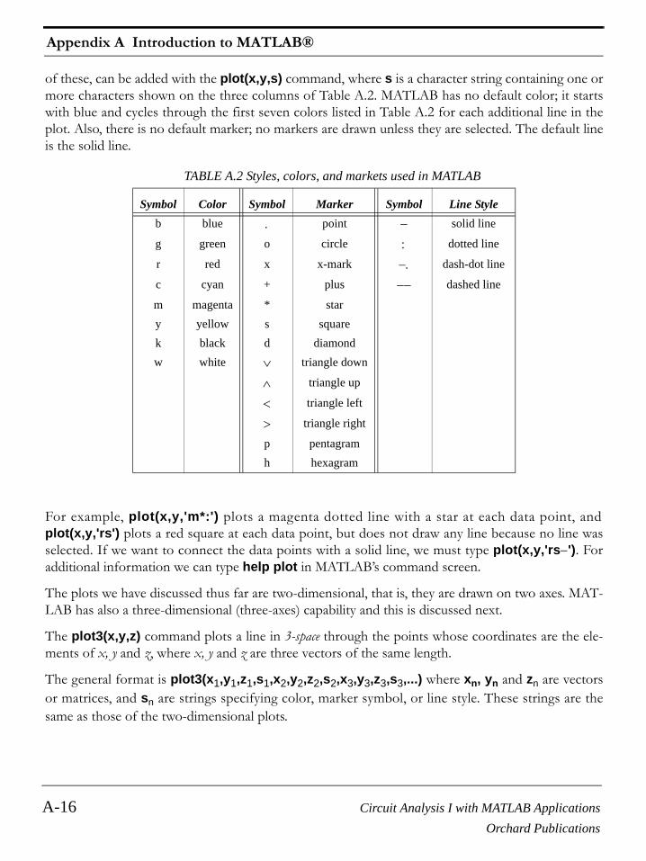
Appendix A Introduction to MATLAB®
A-16 Circuit Analysis I with MATLAB ApplicationsOrchard Publications
of these, can be added with the plot(x,y,s) command, where s is a character string containing one ormore characters shown on the three columns of Table A.2. MATLAB has no default color; it startswith blue and cycles through the first seven colors listed in Table A.2 for each additional line in theplot. Also, there is no default marker; no markers are drawn unless they are selected. The default lineis the solid line.
For example, plot(x,y,'m*:') plots a magenta dotted line with a star at each data point, andplot(x,y,'rs') plots a red square at each data point, but does not draw any line because no line wasselected. If we want to connect the data points with a solid line, we must type plot(x,y,'rs−'). Foradditional information we can type help plot in MATLAB’s command screen.
The plots we have discussed thus far are two-dimensional, that is, they are drawn on two axes. MAT-LAB has also a three-dimensional (three-axes) capability and this is discussed next.
The plot3(x,y,z) command plots a line in 3-space through the points whose coordinates are the ele-ments of x, y and z, where x, y and z are three vectors of the same length.
The general format is plot3(x1,y1,z1,s1,x2,y2,z2,s2,x3,y3,z3,s3,...) where xn, yn and zn are vectorsor matrices, and sn are strings specifying color, marker symbol, or line style. These strings are thesame as those of the two-dimensional plots.
TABLE A.2 Styles, colors, and markets used in MATLAB
Symbol Color Symbol Marker Symbol Line Styleb blue . point − solid line
g green o circle : dotted line
r red x x-mark −. dash-dot line
c cyan + plus −− dashed line
m magenta * stary yellow s squarek black d diamondw white ∨ triangle down
∧ triangle up
< triangle left
> triangle right
p pentagramh hexagram

Circuit Analysis I with MATLAB Applications A-17Orchard Publications
Using MATLAB to Make Plots
Example A.11
Plot the function
(A.3)Solution:
We arbitrarily choose the interval (length) shown on the code below.
x= -10: 0.5: 10; % Length of vector x
y= x; % Length of vector y must be same as x
z= −2.*x.^3+x+3.*y.^2−1; % Vector z is function of both x and y*
plot3(x,y,z); grid
The three-dimensional plot is shown in Figure A.5.
Figure A.5. Three dimensional plot for Example A.11
In a two-dimensional plot, we can set the limits of the x- and y-axes with the axis([xmin xmax yminymax]) command. Likewise, in a three-dimensional plot we can set the limits of all three axes with
* This statement uses the so called dot multiplication, dot division, and dot exponentiation where the multiplication,division, and exponential operators are preceded by a dot. These operations will be explained in Section A.8.
z 2x3– x 3y2 1–+ +=
-10
-5
0
5
10
-10
-5
0
5
10-2000
-1000
0
1000
2000
3000

Appendix A Introduction to MATLAB®
A-18 Circuit Analysis I with MATLAB ApplicationsOrchard Publications
the axis([xmin xmax ymin ymax zmin zmax]) command. It must be placed after the plot(x,y) orplot3(x,y,z) commands, or on the same line without first executing the plot command. This must bedone for each plot. The three-dimensional text(x,y,z,’string’) command will place string beginningat the co-ordinate (x,y,z) on the plot.
For three-dimensional plots, grid on and box off are the default states.
We can also use the mesh(x,y,z) command with two vector arguments. These must be defined as and where . In this case, the vertices of the mesh
lines are the triples . We observe that x corresponds to the columns of Z, and ycorresponds to the rows.
To produce a mesh plot of a function of two variables, say , we must first generate the Xand Y matrices that consist of repeated rows and columns over the range of the variables x and y. Wecan generate the matrices X and Y with the [X,Y]=meshgrid(x,y) function that creates the matrix Xwhose rows are copies of the vector x, and the matrix Y whose columns are copies of the vector y.
Example A.12
The volume of a right circular cone of radius and height is given by
(A.4)
Plot the volume of the cone as and vary on the intervals and meters.
Solution:
The volume of the cone is a function of both the radius r and the height h, that is,
The three-dimensional plot is created with the following MATLAB code where, as in the previousexample, in the second line we have used the dot multiplication, dot division, and dot exponentiation.This will be explained in Section A.8.
[R,H]=meshgrid(0: 4, 0: 6); % Creates R and H matrices from vectors r and h
V=(pi .* R .^ 2 .* H) ./ 3; mesh(R, H, V)
xlabel('x-axis, radius r (meters)'); ylabel('y-axis, altitude h (meters)');
zlabel('z-axis, volume (cubic meters)'); title('Volume of Right Circular Cone'); box on
The three-dimensional plot of Figure A.6, shows how the volume of the cone increases as the radiusand height are increased.
length x( ) n= length y( ) m= m n,[ ] size Z( )=
x j( ) y i( ) Z i j,( ),,
z f x y,( )=
V r h
V 13---πr2h=
r h 0 r 4≤ ≤ 0 h 6≤ ≤
V f r h,( )=

Circuit Analysis I with MATLAB Applications A-19Orchard Publications
Subplots
Figure A.6. Volume of a right circular cone.
This, and the plot of Figure A.5, are rudimentary; MATLAB can generate very sophisticated three-dimensional plots. The MATLAB User’s manual contains more examples.
A.8 Subplots
MATLAB can display up to four windows of different plots on the Figure window using the com-mand subplot(m,n,p). This command divides the window into an m × n matrix of plotting areas andchooses the pth area to be active. No spaces or commas are required between the three integers m, nand p. The possible combinations are shown in Figure A.7.
We will illustrate the use of the subplot(m,n,p) command following the discussion on multiplica-tion, division and exponentiation that follows.
Figure A.7. Possible subplot arrangements in MATLAB
01
23
4
0
2
4
60
20
40
60
80
100
120
x-axis, radius r (meters)
Volume of Right Circular Cone
y-axis, altitude h (meters)
z-ax
is,
volu
me
(cub
ic m
eter
s)
111Full Screen Default
211 212
221 222 223 224
121 122
221 222 212
211 223 224
221 223
122 121 222224
Appendix A Introduction to MATLAB®
A-20 Circuit Analysis I with MATLAB ApplicationsOrchard Publications
A.9 Multiplication, Division and Exponentiation
MATLAB recognizes two types of multiplication, division, and exponentiation. These are the matrixmultiplication, division, and exponentiation, and the element-by-element multiplication, division,and exponentiation. They are explained in the following paragraphs.
In Section A.2, the arrays , such a those that contained the coefficients of polynomials,consisted of one row and multiple columns, and thus are called row vectors. If an array has one col-umn and multiple rows, it is called a column vector. We recall that the elements of a row vector areseparated by spaces. To distinguish between row and column vectors, the elements of a column vec-tor must be separated by semicolons. An easier way to construct a column vector, is to write it first asa row vector, and then transpose it into a column vector. MATLAB uses the single quotation charac-ter (′) to transpose a vector. Thus, a column vector can be written either as b=[−1; 3; 6; 11] or as b=[−1 3 6 11]'. MATLAB produces the same display with either format as shown below.
b=[−1; 3; 6; 11]
b =
-1
3
6
11
b=[−1 3 6 11]'
b =
-1
3
6
11
We will now define Matrix Multiplication and Element-by-Element multiplication.
1. Matrix Multiplication (multiplication of row by column vectors)
Let
and
a b c …[ ]
A a1 a2 a3 … an[ ]=
B b1 b2 b3 … bn[ ]'=

Circuit Analysis I with MATLAB Applications A-21Orchard Publications
Multiplication, Division and Exponentiation
be two vectors. We observe that A is defined as a row vector whereas B is defined as a column vector,as indicated by the transpose operator (′). Here, multiplication of the row vector A by the columnvector B, is performed with the matrix multiplication operator (*). Then,
(A.5)
For example, if
and
the matrix multiplication produces the single value 68, that is,
and this is verified with MATLAB as
A=[1 2 3 4 5]; B=[ −2 6 −3 8 7]';A*B
ans =
68
Now, let us suppose that both A and B are row vectors, and we attempt to perform a row-by-rowmultiplication with the following MATLAB statements.
A=[1 2 3 4 5]; B=[−2 6 −3 8 7];A*B
When these statements are executed, MATLAB displays the following message:
??? Error using ==> *
Inner matrix dimensions must agree.
Here, because we have used the matrix multiplication operator (*) in A*B, MATLAB expects vector Bto be a column vector, not a row vector. It recognizes that B is a row vector, and warns us that wecannot perform this multiplication using the matrix multiplication operator (*). Accordingly, we mustperform this type of multiplication with a different operator. This operator is defined below.
2.Element-by-Element Multiplication (multiplication of a row vector by another row vector)
Let
and
A*B a1b1 a2b2 a3b3 … anbn+ + + +[ ] gle valuesin= =
A 1 2 3 4 5[ ]=
B 2– 6 3– 8 7[ ]'=
A*B
A∗B 1 2–( ) 2 6 3 3–( ) 4 8 5 7×+×+×+×+× 68= =
C c1 c2 c3 … cn[ ]=
D d1 d2 d3 … dn[ ]=

Appendix A Introduction to MATLAB®
A-22 Circuit Analysis I with MATLAB ApplicationsOrchard Publications
be two row vectors. Here, multiplication of the row vector C by the row vector D is performed withthe dot multiplication operator (.*). There is no space between the dot and the multiplication sym-bol. Thus,
(A.6)
This product is another row vector with the same number of elements, as the elements of C and D.
As an example, let
and
Dot multiplication of these two row vectors produce the following result.
Check with MATLAB:
C=[1 2 3 4 5]; % Vectors C and D must haveD=[−2 6 −3 8 7]; % same number of elementsC.*D % We observe that this is a dot multiplication
ans = -2 12 -9 32 35
Similarly, the division (/) and exponentiation (^) operators, are used for matrix division and exponen-tiation, whereas dot division (./) and dot exponentiation (.^) are used for element-by-element divi-sion and exponentiation.
We must remember that no space is allowed between the dot (.) and the multiplication, divi-sion, and exponentiation operators.
Note: A dot (.) is never required with the plus (+) and minus (−) operators.
Example A.13
Write the MATLAB code that produces a simple plot for the waveform defined as
(A.7)
in the seconds interval.
Solution:
The MATLAB code for this example is as follows:
C.∗D c1d1 c2d2 c3d3 … cndn[ ]=
C 1 2 3 4 5[ ]=
D 2– 6 3– 8 7[ ]=
C.∗D 1 2–( )× 2 6× 3 3–( )× 4 8 5 7×× 2– 12 9– 32 35= =
y f t( ) 3e 4t– 5tcos 2e 3t– 2tsin– t2
t 1+-----------+= =
0 t 5≤ ≤

Circuit Analysis I with MATLAB Applications A-23Orchard Publications
Multiplication, Division and Exponentiation
t=0: 0.01: 5 % Define t-axis in 0.01 incrementsy=3 .* exp(−4 .* t) .* cos(5 .* t)−2 .* exp(−3 .* t) .* sin(2 .* t) + t .^2 ./ (t+1);plot(t,y); grid; xlabel('t'); ylabel('y=f(t)'); title('Plot for Example A.13')
Figure A.8 shows the plot for this example.
Figure A.8. Plot for Example A.13
Had we, in this example, defined the time interval starting with a negative value equal to or less than, say as , MATLAB would have displayed the following message:
Warning: Divide by zero.
This is because the last term (the rational fraction) of the given expression, is divided by zero when. To avoid division by zero, we use the special MATLAB function eps, which is a number
approximately equal to . It will be used with the next example.
The command axis([xmin xmax ymin ymax]) scales the current plot to the values specified by thearguments xmin, xmax, ymin and ymax. There are no commas between these four arguments.This command must be placed after the plot command and must be repeated for each plot.
The following example illustrates the use of the dot multiplication, division, and exponentiation, theeps number, the axis([xmin xmax ymin ymax]) command, and also MATLAB’s capability of dis-playing up to four windows of different plots.
Example A.14
Plot the functions
0 0.5 1 1.5 2 2.5 3 3.5 4 4.5 5-1
0
1
2
3
4
5
t
y=f(t
)Plot for Example A.13
1– 3 t 3≤ ≤–
t 1–=
2.2 10 16–×

Appendix A Introduction to MATLAB®
A-24 Circuit Analysis I with MATLAB ApplicationsOrchard Publications
in the interval using 100 data points. Use the subplot command to display these func-tions on four windows on the same graph.
Solution:
The MATLAB code to produce the four subplots is as follows:
x=linspace(0,2*pi,100); % Interval with 100 data pointsy=(sin(x).^ 2); z=(cos(x).^ 2); w=y.* z;v=y./ (z+eps); % add eps to avoid division by zerosubplot(221);% upper left of four subplotsplot(x,y); axis([0 2*pi 0 1]);title('y=(sinx)^2');subplot(222); % upper right of four subplotsplot(x,z); axis([0 2*pi 0 1]); title('z=(cosx)^2');subplot(223); % lower left of four subplotsplot(x,w); axis([0 2*pi 0 0.3]);title('w=(sinx)^2*(cosx)^2');subplot(224); % lower right of four subplotsplot(x,v); axis([0 2*pi 0 400]);title('v=(sinx)^2/(cosx)^2');
These subplots are shown in Figure A.9.
Figure A.9. Subplots for the functions of Example A.14
y x2sin z, x2cos w, x2sin x2cos⋅ v, x2sin x2cos⁄= = = =
0 x 2π≤ ≤
0 2 4 60
0.2
0.4
0.6
0.8
1y=(sinx)2
0 2 4 60
0.2
0.4
0.6
0.8
1z=(cosx)2
0 2 4 60
0.05
0.1
0.15
0.2
0.25
w=(sinx)2*(cosx)2
0 2 4 60
100
200
300
400v=(sinx)2/(cosx)2

Circuit Analysis I with MATLAB Applications A-25Orchard Publications
Multiplication, Division and Exponentiation
The next example illustrates MATLAB’s capabilities with imaginary numbers. We will introduce thereal(z) and imag(z) functions that display the real and imaginary parts of the complex quantity z =x + iy, the abs(z), and the angle(z) functions that compute the absolute value (magnitude) andphase angle of the complex quantity z = x + iy = r∠θ. We will also use the polar(theta,r) functionthat produces a plot in polar coordinates, where r is the magnitude, theta is the angle in radians, andthe round(n) function that rounds a number to its nearest integer.
Example A.15
Consider the electric circuit of Figure A.10.
Figure A.10. Electric circuit for Example A.15
With the given values of resistance, inductance, and capacitance, the impedance as a function ofthe radian frequency ω can be computed from the following expression:
(A.8)
a. Plot (the real part of the impedance Z) versus frequency ω.
b. Plot (the imaginary part of the impedance Z) versus frequency ω.
c. Plot the impedance Z versus frequency ω in polar coordinates.
Solution:
The MATLAB code below computes the real and imaginary parts of that is, for simplicity,denoted as z, and plots these as two separate graphs (parts a & b). It also produces a polar plot (partc).
w=0: 1: 2000; % Define interval with one radian intervalz=(10+(10 .^ 4 −j .* 10 .^ 6 ./ (w+eps)) ./ (10 + j .* (0.1 .* w −10.^5./ (w+eps))));%% The first five statements (next two lines) compute and plot Rezreal_part=real(z); plot(w,real_part); grid;xlabel('radian frequency w'); ylabel('Real part of Z');%
a
b
10 Ω
10 Ω
0.1 H
10 µFZab
Zab
Zab Z 10 104 j 106 ω⁄( )–
10 j 0.1ω 105 ω⁄ –( )+--------------------------------------------------------+= =
Re Z
Im Z
Zab
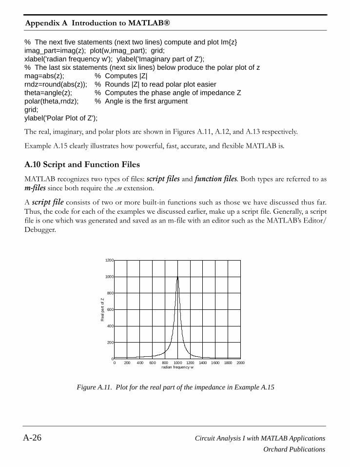
Appendix A Introduction to MATLAB®
A-26 Circuit Analysis I with MATLAB ApplicationsOrchard Publications
% The next five statements (next two lines) compute and plot Imzimag_part=imag(z); plot(w,imag_part); grid;xlabel('radian frequency w'); ylabel('Imaginary part of Z');% The last six statements (next six lines) below produce the polar plot of zmag=abs(z); % Computes |Z|rndz=round(abs(z)); % Rounds |Z| to read polar plot easiertheta=angle(z); % Computes the phase angle of impedance Zpolar(theta,rndz); % Angle is the first argumentgrid;ylabel('Polar Plot of Z');
The real, imaginary, and polar plots are shown in Figures A.11, A.12, and A.13 respectively.
Example A.15 clearly illustrates how powerful, fast, accurate, and flexible MATLAB is.
A.10 Script and Function Files
MATLAB recognizes two types of files: script files and function files. Both types are referred to asm-files since both require the .m extension.
A script file consists of two or more built-in functions such as those we have discussed thus far.Thus, the code for each of the examples we discussed earlier, make up a script file. Generally, a scriptfile is one which was generated and saved as an m-file with an editor such as the MATLAB’s Editor/Debugger.
Figure A.11. Plot for the real part of the impedance in Example A.15
0 200 400 600 800 1000 1200 1400 1600 1800 20000
200
400
600
800
1000
1200
radian frequency w
Rea
l pa
rt of
Z

Circuit Analysis I with MATLAB Applications A-27Orchard Publications
Script and Function Files
Figure A.12. Plot for the imaginary part of the impedance in Example A.15
Figure A.13. Polar plot of the impedance in Example A.15
0 200 400 600 800 1000 1200 1400 1600 1800 2000-600
-400
-200
0
200
400
600
radian frequency w
Imag
ina
ry p
art
of Z
Pol
ar P
lot
of Z 203
406
609
812
1015
30
210
60
240
90
270
120
300
150
330
180 0

Appendix A Introduction to MATLAB®
A-28 Circuit Analysis I with MATLAB ApplicationsOrchard Publications
A function file is a user-defined function using MATLAB. We use function files for repetitive tasks.The first line of a function file must contain the word function, followed by the output argument, theequal sign ( = ), and the input argument enclosed in parentheses. The function name and file namemust be the same, but the file name must have the extension .m. For example, the function file con-sisting of the two lines below
function y = myfunction(x)
y=x.^ 3 + cos(3.* x)
is a function file and must be saved as myfunction.m
For the next example, we will use the following MATLAB functions.
fzero(f,x) tries to find a zero of a function of one variable, where f is a string containing the name ofa real-valued function of a single real variable. MATLAB searches for a value near a point where thefunction f changes sign, and returns that value, or returns NaN if the search fails.
Important: We must remember that we use roots(p) to find the roots of polynomials only, such asthose in Examples A.1 and A.2.
fmin(f,x1,x2) minimizes a function of one variable. It attempts to return a value of x where isminimum in the interval . The string f contains the name of the function to be minimized.
Note: MATLAB does not have a function to maximize a function of one variable, that is, there is nofmax(f,x1,x2) function in MATLAB; but since a maximum of is equal to a minimum of ,we can use fmin(f,x1,x2) to find both minimum and maximum values of a function.
fplot(fcn,lims) plots the function specified by the string fcn between the x-axis limits specified bylims = [xmin xmax]. Using lims = [xmin xmax ymin ymax] also controls the y-axis limits. Thestring fcn must be the name of an m-file function or a string with variable .
Note: NaN (Not-a-Number) is not a function; it is MATLAB’s response to an undefined expressionsuch as , , or inability to produce a result as described on the next paragraph. We can avoiddivision by zero using the eps number, that we mentioned earlier.
Example A.16
Find the zeros, maxima and minima of the function
Solution:
We first plot this function to observe the approximate zeros, maxima, and minima using the follow-ing code.
f x( )x1 x x2< <
f x( ) f x( )–
x
0 0⁄ ∞ ∞⁄
f x( ) 1x 0.1–( )2 0.01+
---------------------------------------- 1x 1.2–( )2 0.04+
---------------------------------------- 10–+=

Circuit Analysis I with MATLAB Applications A-29Orchard Publications
Script and Function Files
x=−1.5: 0.01: 1.5;y=1./ ((x−0.1).^ 2 + 0.01) −1./ ((x−1.2).^ 2 + 0.04) −10;plot(x,y); grid
The plot is shown in Figure A.14.
Figure A.14. Plot for Example A.16 using the plot command
The roots (zeros) of this function appear to be in the neighborhood of and . Themaximum occurs at approximately where, approximately, , and the minimumoccurs at approximately where, approximately, .
Next, we define and save f(x) as the funczero01.m function m-file with the following code:
function y=funczero01(x)
% Finding the zeros of the function shown below
y=1/((x−0.1)^2+0.01)−1/((x−1.2)^2+0.04)-10;
Now, we can use the fplot(fcn,lims) command to plot as follows.
fplot('funczero01', [−1.5 1.5]); grid
This plot is shown in Figure A.15. As expected, this plot is identical to the plot of Figure A.14 thatwas obtained with the plot(x,y) command.
-1.5 -1 -0.5 0 0.5 1 1.5-40
-20
0
20
40
60
80
100
x 0.2–= x 0.3=
x 0.1= ymax 90=
x 1.2= ymin 34–=
f x( )

Appendix A Introduction to MATLAB®
A-30 Circuit Analysis I with MATLAB ApplicationsOrchard Publications
Figure A.15. Plot for Example A.16 using the fplot command
We will use the fzero(f,x) function to compute the roots of in (A.20) more precisely. The codebelow must be saved with a file name, and then invoked with that file name.
x1= fzero('funczero01', -0.2);x2= fzero('funczero01', 0.3);fprintf('The roots (zeros) of this function are r1= %3.4f', x1);fprintf(' and r2= %3.4f \n', x2)
MATLAB displays the following:
The roots (zeros) of this function are r1= -0.1919 and r2= 0.3788
Whenever we use the fmin(f,x1,x2) function, we must remember that this function searches for aminimum and it may display the values of local minima* , if any, before displaying the function mini-mum. It is, therefore, advisable to plot the function with either the plot(x,y) or the fplot(fcn,lims)command to find the smallest possible interval within which the function minimum lies. For thisexample, we specify the range rather than the interval .
The minimum of f(x) is found with the fmin(f,x1,x2) function as follows.min_val=fmin('funczero01', 0, 1.5)
min_val = 1.2012
* Local maxima or local minima, are the maximum or minimum values of a function within a restricted range ofvalues in the independent variable. When the entire range is considered, the maxima and minima are consideredbe to the maximum and minimum values in the entire range in which the function is defined.
-1.5 -1 -0.5 0 0.5 1 1.5-40
-20
0
20
40
60
80
100
f x( )
0 x 1.5≤ ≤ 1.5 x 1.5≤ ≤–

Circuit Analysis I with MATLAB Applications A-31Orchard Publications
Display Formats
This is the value of x at which is minimum. To find the value of y corresponding to thisvalue of x, we substitute it into , that is,
x=1.2012; y=1 / ((x−0.1) ^ 2 + 0.01) −1 / ((x−1.2) ^ 2 + 0.04) −10
y = -34.1812
To find the maximum value, we must first define a new function m-file that will produce . Wedefine it as follows:
function y=minusfunczero01(x)
% It is used to find maximum value from -f(x)
y=−(1/((x−0.1)^2+0.01)−1/((x−1.2)^2+0.04)−10);
We have placed the minus (−) sign in front of the right side of the last expression above, so that themaximum value will be displayed. Of course, this is equivalent to the negative of the funczero01function.
Now, we execute the following code to get the value of x where the maximum occurs.
max_val=fmin('minusfunczero01', 0,1)
max_val = 0.0999
x=0.0999;% Using this value find the corresponding value of yy=1 / ((x−0.1) ^ 2 + 0.01) −1 / ((x−1.2) ^ 2 + 0.04) −10
y = 89.2000
A.11 Display Formats
MATLAB displays the results on the screen in integer format without decimals if the result is an inte-ger number, or in short floating point format with four decimals if it a fractional number. The formatdisplayed has nothing to do with the accuracy in the computations. MATLAB performs all computa-tions with accuracy up to 16 decimal places.
The output format can changed with the format command. The available formats can be displayedwith the help format command as follows:
help format
FORMAT Set output format.
All computations in MATLAB are done in double precision.
FORMAT may be used to switch between different output display formats as follows:
FORMAT Default. Same as SHORT.
y f x( )=
f x( )
f x( )–
y f x( )=

Appendix A Introduction to MATLAB®
A-32 Circuit Analysis I with MATLAB ApplicationsOrchard Publications
FORMAT SHORT Scaled fixed point format with 5 digits.
FORMAT LONG Scaled fixed point format with 15 digits.
FORMAT SHORT E Floating point format with 5 digits.
FORMAT LONG E Floating point format with 15 digits.
FORMAT SHORT G Best of fixed or floating point format with 5 digits.
FORMAT LONG G Best of fixed or floating point format with 15 digits.
FORMAT HEX Hexadecimal format.
FORMAT + The symbols +, - and blank are printed for positive, negative and zero elements. Imaginary parts are ignored.
FORMAT BANK Fixed format for dollars and cents.
FORMAT RAT Approximation by ratio of small integers.
Spacing:
FORMAT COMPACT Suppress extra line-feeds.
FORMAT LOOSE Puts the extra line-feeds back in.
Some examples with different format displays age given below.
format short 33.3335 Four decimal digits (default)
format long 33.33333333333334 16 digits
format short e 3.3333e+01 Four decimal digits plus exponent
format short g 33.333 Better of format short or format short e
format bank 33.33 two decimal digits
format + only + or − or zero are printed
format rat 100/3 rational approximation
The disp(X) command displays the array X without printing the array name. If X is a string, the textis displayed.
The fprintf(format,array) command displays and prints both text and arrays. It uses specifiers toindicate where and in which format the values would be displayed and printed. Thus, if %f is used,the values will be displayed and printed in fixed decimal format, and if %e is used, the values will bedisplayed and printed in scientific notation format. With this command only the real part of eachparameter is processed.

Circuit Analysis I with MATLAB Applications B-1Orchard Publications
Appendix B
A Review of Complex Numbers
his appendix is a review of the algebra of complex numbers. The basic operations are definedand illustrated by several examples. Applications using Euler’s identities are presented, and theexponential and polar forms are discussed and illustrated with examples.
B.1 Definition of a Complex Number
In the language of mathematics, the square root of minus one is denoted as , that is, . Inthe electrical engineering field, we denote as to avoid confusion with current . Essentially, isan operator that produces a 90-degree counterclockwise rotation to any vector to which it is appliedas a multiplying factor. Thus, if it is given that a vector has the direction along the right side of thex-axis as shown in Figure B.1, multiplication of this vector by the operator will result in a new vec-tor whose magnitude remains the same, but it has been rotated counterclockwise by . Also,another multiplication of the new vector by will produce another counterclockwise direc-tion. In this case, the vector has rotated and its new value now is . When this vector isrotated by another for a total of , its value becomes . A fourth rotationreturns the vector to its original position, and thus its value is again . Therefore, we conclude that
, , and .
Figure B.1. The j operator
Ti i 1–=
i j i j
Aj
jA 90°jA j 90°
A 180° A–
90° 270° j A–( ) jA–= 90°A
j 2 1–= j 3 j–= j 4 1=
x
yjA
j jA( ) j2A A–= =
j A–( ) j 3A jA–= =
j jA–( ) j– 2A A= =
A

Appendix B A Review of Complex Numbers
B-2 Circuit Analysis I with MATLAB ApplicationsOrchard Publications
Note: In our subsequent discussion, we will designate the x-axis (abscissa) as the real axis, and the y-axis (ordinate) as the imaginary axis with the understanding that the “imaginary” axis is just as “real”as the real axis. In other words, the imaginary axis is just as important as the real axis.*
An imaginary number is the product of a real number, say , by the operator . Thus, is a real numberand is an imaginary number.
A complex number is the sum (or difference) of a real number and an imaginary number. For example,the number where and are both real numbers, is a complex number. Then,
and where denotes real part of A, and the imagi-nary part of A.
By definition, two complex numbers and where and , are equal if andonly if their real parts are equal, and also their imaginary parts are equal. Thus, if and only if
and .
B.2 Addition and Subtraction of Complex Numbers
The sum of two complex numbers has a real component equal to the sum of the real components,and an imaginary component equal to the sum of the imaginary components. For subtraction, wechange the signs of the components of the subtrahend and we perform addition. Thus, if
and then
and
Example B.1
It is given that , and . Find and
Solution:
and
* We may think the real axis as the cosine axis and the imaginary axis as the sine axis.
r j rjr
A a jb+= a ba Re A = b Im A = Re A b Im A =
A B A a jb+= B c jd+=A B=
a c= b d=
A a jb+= B c jd+=
A B+ a c+( ) j b d+( )+=
A B– a c–( ) j b d–( )+=
A 3 j4+= B 4 j2–= A B+ A B–
A B+ 3 j4+( )= 4 j2–( )+ 3 4+( ) j 4 2–( )+ 7 j2+= =
A B– 3 j4+( )= 4 j2–( )– 3 4–( ) j 4 2+( )+ 1– j6+= =

Circuit Analysis I with MATLAB Applications B-3Orchard Publications
Multiplication of Complex Numbers
B.3 Multiplication of Complex Numbers
Complex numbers are multiplied using the rules of elementary algebra, and making use of the factthat . Thus, if
and then
and since , it follows that
(B.1)
Example B.2
It is given that and . Find
Solution:
The conjugate of a complex number, denoted as , is another complex number with the same realcomponent, and with an imaginary component of opposite sign. Thus, if , then
.
Example B.3
It is given that . Find
Solution:
The conjugate of the complex number A has the same real component, but the imaginary compo-nent has opposite sign. Then,
If a complex number A is multiplied by its conjugate, the result is a real number. Thus, if , then
Example B.4
It is given that . Find
Solution:
j 2 1–=
A a jb+= B c jd+=
A B⋅ a jb+( ) c jd+( )⋅ ac jad jbc j2bd+ + += =
j 2 1–=
A B⋅ ac jad jbc b– d+ +=
ac bd–( ) j ad bc+( )+=
A 3 j4+= B 4 j2–= A B⋅
A B⋅ 3 j4+( ) 4 j2–( )⋅ 12 j6– j16 j 28–+ 20 j10+= = =
A∗A a jb+=
A∗ a j– b=
A 3 j5+= A∗
A∗ 3 j– 5=
A a jb+=
A A∗⋅ a jb+( ) a jb–( ) a2 jab– jab j 2b2–+ a2 b2+= = =
A 3 j5+= A A∗⋅
A A∗⋅ 3 j5+( ) 3 j5–( ) 32 52+ 9 25 34=+= = =
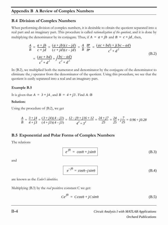
Appendix B A Review of Complex Numbers
B-4 Circuit Analysis I with MATLAB ApplicationsOrchard Publications
B.4 Division of Complex Numbers
When performing division of complex numbers, it is desirable to obtain the quotient separated into areal part and an imaginary part. This procedure is called rationalization of the quotient, and it is done bymultiplying the denominator by its conjugate. Thus, if and , then,
(B.2)
In (B.2), we multiplied both the numerator and denominator by the conjugate of the denominator toeliminate the j operator from the denominator of the quotient. Using this procedure, we see that thequotient is easily separated into a real and an imaginary part.
Example B.5
It is given that , and . Find
Solution:
Using the procedure of (B.2), we get
B.5 Exponential and Polar Forms of Complex Numbers
The relations
(B.3)
and
(B.4)
are known as the Euler’s identities.
Multiplying (B.3) by the real positive constant C we get:
(B.5)
A a jb+= B c jd+=
AB--- a jb+
c jd+-------------- a jb+( ) c jd–( )
c jd+( ) c jd–( )-------------------------------------- A
B--- B∗
B∗------⋅ ac bd+( ) j bc ad–( )+
c2 d 2+-------------------------------------------------------= = = =
ac bd+( )c2 d 2+
----------------------- j bc ad–( )c2 d 2+
-----------------------+=
A 3 j4+= B 4 j3+= A B⁄
AB--- 3 j4+
4 j3+-------------- 3 j4+( ) 4 j3–( )
4 j3+( ) 4 j3–( )-------------------------------------- 12 j9– j16 12+ +
42 32+
-------------------------------------------- 24 j7+25
----------------- 2425------ j 7
25------+ 0.96 j0.28+= = = = ==
e jθθ j θsin+cos=
e jθ–θ j– θsincos=
Ce jθ C θ jC θsin+cos=

Circuit Analysis I with MATLAB Applications B-5Orchard Publications
Exponential and Polar Forms of Complex Numbers
This expression represents a complex number, say , and thus
(B.6)
where the left side of (B.6) is the exponential form, and the right side is the rectangular form.
Equating real and imaginary parts in (B.5) and (B.6), we get
(B.7)
Squaring and adding the expressions in (B.7), we get
Then,
or
(B.8)
Also, from (B.7)
or
(B.9)
To convert a complex number from rectangular to exponential form, we use the expression
(B.10)
To convert a complex number from exponential to rectangular form, we use the expressions
(B.11)
The polar form is essentially the same as the exponential form but the notation is different, that is,
(B.12)
a jb+
Ce jθ a jb+=
a C θcos= and b C θsin=
a2 b2+ C θcos( )2 C θsin( )2+ C2 θ2cos θ2sin+( ) C2= = =
C2 a2 b2+=
C a2 b2+=
ba--- C θsin
C θcos--------------- θtan= =
θ ba---⎝ ⎠
⎛ ⎞1–tan=
a jb+ a2 b2+ ej tan 1– b
a---⎝ ⎠
⎛ ⎞=
Ce jθ C θ jC θsin+cos=
Ce jθ– C θ j– C θsincos=
Ce jθ C θ∠=
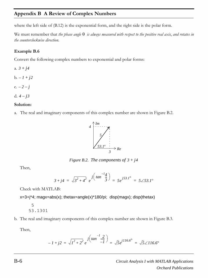
Appendix B A Review of Complex Numbers
B-6 Circuit Analysis I with MATLAB ApplicationsOrchard Publications
where the left side of (B.12) is the exponential form, and the right side is the polar form.
We must remember that the phase angle is always measured with respect to the positive real axis, and rotates inthe counterclockwise direction.
Example B.6
Convert the following complex numbers to exponential and polar forms:
a.
b.
c.
d.
Solution:
a. The real and imaginary components of this complex number are shown in Figure B.2.
Figure B.2. The components of
Then,
Check with MATLAB:
x=3+j*4; magx=abs(x); thetax=angle(x)*180/pi; disp(magx); disp(thetax)
5 53.1301
b. The real and imaginary components of this complex number are shown in Figure B.3.
Then,
θ
3 j4+
1– j2+
2– j–
4 j3–
Re
Im4
3
5
53.1°
3 j4+
3 j4+ 32 42+ e
j 43---
1–tan⎝ ⎠
⎛ ⎞5e j53.1° 5 53.1°∠= = =
1– j2+ 12 22+ ej 2
1–------
1–tan⎝ ⎠
⎛ ⎞5ej116.6° 5 116.6°∠= = =
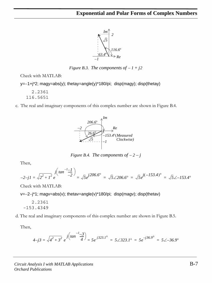
Circuit Analysis I with MATLAB Applications B-7Orchard Publications
Exponential and Polar Forms of Complex Numbers
Figure B.3. The components of
Check with MATLAB:
y=−1+j*2; magy=abs(y); thetay=angle(y)*180/pi; disp(magy); disp(thetay)
2.2361 116.5651
c. The real and imaginary components of this complex number are shown in Figure B.4.
Figure B.4. The components of
Then,
Check with MATLAB:
v=−2−j*1; magv=abs(v); thetav=angle(v)*180/pi; disp(magv); disp(thetav)
2.2361 -153.4349
d. The real and imaginary components of this complex number are shown in Figure B.5.
Then,
Re
Im2
−1
116.6°63.4°
5
1– j2+
Re
Im
−2
−1
206.6°
−153.4°(Measured26.6°
Clockwise)5
2– j–
2– j– 1 22 12+ e
j 1–2–
------1–
tan⎝ ⎠⎛ ⎞
5ej206.6°= = 5 206.6°∠ 5ej 153.4–( )° 5 153.4– °∠= = =
4 j– 3 42 32+ e
j 3–4
------1–
tan⎝ ⎠⎛ ⎞
5e j323.1°= = 5 323.1°∠ 5e j36.9– ° 5 36.9– °∠= = =

Appendix B A Review of Complex Numbers
B-8 Circuit Analysis I with MATLAB ApplicationsOrchard Publications
Figure B.5. The components of
Check with MATLAB:
w=4−j*3; magw=abs(w); thetaw=angle(w)*180/pi; disp(magw); disp(thetaw)
5 -36.8699
Example B.7
Express the complex number in exponential and in rectangular forms.
Solution:
We recall that . Since each rotates a vector by counterclockwise, then is thesame as rotated counterclockwise by . Therefore,
The components of this complex number are shown in Figure B.6.
Figure B.6. The components of
Then,
Note: The rectangular form is most useful when we add or subtract complex numbers; however, theexponential and polar forms are most convenient when we multiply or divide complex numbers.
To multiply two complex numbers in exponential (or polar) form, we multiply the magnitudes andwe add the phase angles, that is, if
Re
Im4
−35
323.1°
−36.9°
4 j3–
2 30°∠–
1– j2= j 90° 2 30°∠–
2 30°∠ 180°
2 30°∠– 2 30° 180°+( )∠ 2 210°∠ 2 150°–∠= = =
Re
Im
−1.73
−1
210°
2−150°(Measured
30°
Clockwise)
2 150°–∠
2 150– °∠ 2e j– 150°= 2 150° j 150°sin–cos( ) 2 0.866– j0.5–( ) 1.73– j–= = =
A M θ∠= and B N φ∠=

Circuit Analysis I with MATLAB Applications B-9Orchard Publications
Exponential and Polar Forms of Complex Numbers
then,
(B.13)
Example B.8
Multiply by
Solution:
Multiplication in polar form yields
and multiplication in exponential form yields
To divide one complex number by another when both are expressed in exponential or polar form,we divide the magnitude of the dividend by the magnitude of the divisor, and we subtract the phaseangle of the divisor from the phase angle of the dividend, that is, if
then,
(B.14)
Example B.9
Divide by
Solution:
Division in polar form yields
Division in exponential form yields
AB MN θ φ+( )∠ Me jθNe jφ MNe j θ φ+( )= = =
A 10 53.1°∠= B 5 36.9°–∠=
AB 10 5×( ) 53.1° 36.9°–( )+[ ]∠ 50 16.2°∠= =
AB 10e j53.1°( ) 5e j– 36.9°( ) 50e j 53.1° 36.9°–( ) 50e j16.2°= = =
A M θ∠= and B N φ∠=
AB--- M
N----- θ φ–( )∠ Me jθ
Ne jφ------------- M
N----e j θ φ–( )
= = =
A 10 53.1°∠= B 5 36.9°–∠=
AB--- 10 53.1°∠
5 36.9°–∠------------------------ 2 53.1° 36.9°–( )–[ ]∠ 2 90°∠= = =
AB--- 10e j53.1°
5e j36.9°–--------------------- 2e j53.1°e j36.9° 2e j90°
= ==

Appendix B A Review of Complex Numbers
B-10 Circuit Analysis I with MATLAB ApplicationsOrchard Publications
NOTES

Circuit Analysis I with MATLAB Applications C-1Orchard Publications
Appendix C
Matrices and Determinants
his chapter is an introduction to matrices and matrix operations. Determinants, Cramer’s rule,and Gauss’s elimination method are reviewed. Some definitions and examples are not applica-ble to subsequent material presented in this text, but are included for subject continuity, and
reference to more advance topics in matrix theory. These are denoted with a dagger (†) and may beskipped.
C.1 Matrix Definition
A matrix is a rectangular array of numbers such as those shown below.
In general form, a matrix A is denoted as
(C.1)
The numbers are the elements of the matrix where the index i indicates the row, and j indicates thecolumn in which each element is positioned. Thus, indicates the element positioned in thefourth row and third column.
A matrix of m rows and n columns is said to be of order matrix.
If , the matrix is said to be a square matrix of order m (or n). Thus, if a matrix has five rows andfive columns, it is said to be a square matrix of order 5.
In a square matrix, the elements are called the main diagonal elements. Alter-nately, we say that the matrix elements , are located on the main diagonal.
T
2 3 71 1– 5
or1 3 12– 1 5–
4 7– 6
A
a11 a12 a13 … a1n
a21 a22 a23 … a2n
a31 a32 a33 … a3n
… … … … …am1 am2 am3 … amn
=
aij
a43
m n×
m n=
a11 a22 a33 … ann, , , ,
a11 a22 a33 … ann, , , ,

Appendix C Matrices and Determinants
C-2 Circuit Analysis I with MATLAB ApplicationsOrchard Publications
† The sum of the diagonal elements of a square matrix is called the trace* of .
† A matrix in which every element is zero, is called a zero matrix.
C.2 Matrix Operations
Two matrices and are equal, that is, , if and only if
(C.2)
Two matrices are said to be conformable for addition (subtraction), if they are of the same order m × n.
If and are conformable for addition (subtraction), their sum (difference) will be
another matrix with the same order as and , where each element of is the sum (difference)of the corresponding elements of and , that is,
(C.3)
Example C.1
Compute and given that
and
Solution:
and
Check with MATLAB:
A=[1 2 3; 0 1 4]; B=[2 3 0; −1 2 5]; % Define matrices A and BA+B % Add A and B
* Henceforth, all paragraphs and topics preceded by a dagger ( † ) may be skipped. These are discussed in matrixtheory textbooks.
A A
A aij= B bij= A B=
aij bij= i 1 2 3 … m, , , ,= j 1 2 3 … n, , , ,=
A aij= B bij=
C A B CA B
C A B± aij bij±[ ]= =
A B+ A B–
A 1 2 30 1 4
= B 2 3 01– 2 5
=
A B+ 1 2+ 2 3+ 3 0+
0 1– 1 2+ 4 5+
3 5 31– 3 9
= =
A B– 1 2– 2 3– 3 0–
0 1+ 1 2– 4 5–
1– 1– 31 1– 1–
= =

Circuit Analysis I with MATLAB Applications C-3Orchard Publications
Matrix Operations
ans = 3 5 3 -1 3 9
A−B % Subtract B from A
ans = -1 -1 3 1 -1 -1
If is any scalar (a positive or negative number), and not [k] which is a matrix, then multipli-cation of a matrix by the scalar is the multiplication of every element of by .
Example C.2
Multiply the matrix
by
a.
b.
Solution:
a.
b.
Check with MATLAB:
k1=5; k2=(−3 + 2*j); % Define scalars k1 and k2A=[1 −2; 2 3]; % Define matrix Ak1*A % Multiply matrix A by constant k1
ans = 5 -10
k 1 1×A k A k
A 1 2–
2 3=
k1 5=
k2 3– j2+=
k1 A⋅ 5 1 2–
2 3× 5 1× 5 2–( )×
5 2× 5 3×5 10–
10 15= = =
k2 A⋅ 3– j2+( ) 1 2–
2 3× 3– j2+( ) 1× 3– j2+( ) 2–( )×
3– j2+( ) 2× 3– j2+( ) 3×3– j2+ 6 j4–
6– j4+ 9– j6+= = =
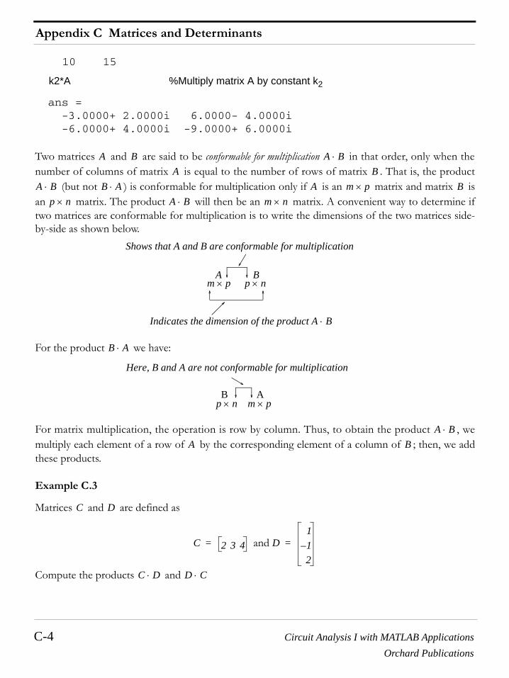
Appendix C Matrices and Determinants
C-4 Circuit Analysis I with MATLAB ApplicationsOrchard Publications
10 15
k2*A %Multiply matrix A by constant k2
ans = -3.0000+ 2.0000i 6.0000- 4.0000i -6.0000+ 4.0000i -9.0000+ 6.0000i
Two matrices and are said to be conformable for multiplication in that order, only when thenumber of columns of matrix is equal to the number of rows of matrix . That is, the product
(but not ) is conformable for multiplication only if is an matrix and matrix isan matrix. The product will then be an matrix. A convenient way to determine iftwo matrices are conformable for multiplication is to write the dimensions of the two matrices side-by-side as shown below.
For the product we have:
For matrix multiplication, the operation is row by column. Thus, to obtain the product , wemultiply each element of a row of by the corresponding element of a column of ; then, we addthese products.
Example C.3
Matrices and are defined as
and
Compute the products and
A B A B⋅A B
A B⋅ B A⋅ A m p× Bp n× A B⋅ m n×
m × p p × nA B
Shows that A and B are conformable for multiplication
Indicates the dimension of the product A ⋅ B
B A⋅
Here, B and A are not conformable for multiplication
B A p × n m × p
A B⋅A B
C D
C 2 3 4= D11–
2
=
C D⋅ D C⋅
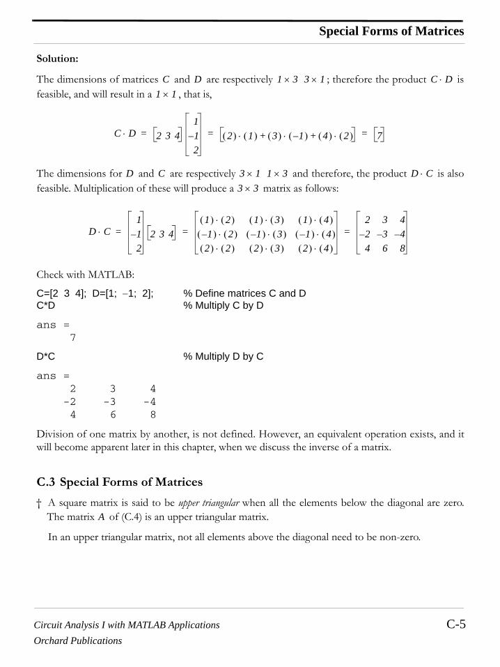
Circuit Analysis I with MATLAB Applications C-5Orchard Publications
Special Forms of Matrices
Solution:
The dimensions of matrices and are respectively ; therefore the product isfeasible, and will result in a , that is,
The dimensions for and are respectively and therefore, the product is alsofeasible. Multiplication of these will produce a matrix as follows:
Check with MATLAB:
C=[2 3 4]; D=[1; −1; 2]; % Define matrices C and DC*D % Multiply C by D
ans = 7
D*C % Multiply D by C
ans = 2 3 4 -2 -3 -4 4 6 8
Division of one matrix by another, is not defined. However, an equivalent operation exists, and itwill become apparent later in this chapter, when we discuss the inverse of a matrix.
C.3 Special Forms of Matrices
† A square matrix is said to be upper triangular when all the elements below the diagonal are zero.The matrix of (C.4) is an upper triangular matrix.
In an upper triangular matrix, not all elements above the diagonal need to be non-zero.
C D 1 3 3 1×× C D⋅1 1×
C D⋅ 2 3 411–
22( ) 1( )⋅ 3( ) 1–( )⋅ 4( ) 2( )⋅+ + 7= = =
D C 3 1 1 3×× D C⋅3 3×
D C⋅11–
22 3 4
1( ) 2( )⋅ 1( ) 3( )⋅ 1( ) 4( )⋅1–( ) 2( )⋅ 1–( ) 3( )⋅ 1–( ) 4( )⋅
2( ) 2( )⋅ 2( ) 3( )⋅ 2( ) 4( )⋅
2 3 42– 3– 4–
4 6 8
= = =
A

Appendix C Matrices and Determinants
C-6 Circuit Analysis I with MATLAB ApplicationsOrchard Publications
(C.4)
† A square matrix is said to be lower triangular, when all the elements above the diagonal are zero. Thematrix of (C.5) is a lower triangular matrix.
(C.5)
In a lower triangular matrix, not all elements below the diagonal need to be non-zero.
† A square matrix is said to be diagonal, if all elements are zero, except those in the diagonal. Thematrix of (C.6) is a diagonal matrix.
(C.6)
† A diagonal matrix is called a scalar matrix, if where k is a scalar.
The matrix of (C.7) is a scalar matrix with k = 4.
(C.7)
A scalar matrix with , is called an identity matrix . Shown below are , , and identity matrices.
A
a11 a12 a13 … a1n
0 a22 a23 … a2n
0 0 … … …… … 0 … …0 0 0 … amn
=
B
B
a11 0 0 … 0a21 a22 0 … 0… … … 0 0… … … … 0
am1 am2 am3 … amn
=
C
C
a11 0 0 … 00 a22 0 … 00 0 … 0 00 0 0 … 00 0 0 … amn
=
a11 a22 a33 … ann k= = = = =
D
D
4 0 0 00 4 0 00 0 4 00 0 0 4
=
k 1= I 2 2× 3 3× 4 4×

Circuit Analysis I with MATLAB Applications C-7Orchard Publications
Special Forms of Matrices
(C.8)
The MATLAB eye(n) function displays an identity matrix. For example,
eye(4) % Display a 4 by 4 identity matrix
ans =
1 0 0 0 0 1 0 0 0 0 1 0 0 0 0 1
Likewise, the eye(size(A)) function, produces an identity matrix whose size is the same as matrix. For example, let matrix be defined as
A=[1 3 1; −2 1 −5; 4 −7 6] % Define matrix A
A = 1 3 1 -2 1 -5 4 -7 6then,
eye(size(A))
displays
ans =
1 0 0 0 1 0 0 0 1
† The transpose of a matrix , denoted as , is the matrix that is obtained when the rows and col-umns of matrix are interchanged. For example, if
(C.9)
1 00 1
1 0 00 1 00 0 1
1 0 0 00 1 0 00 0 1 00 0 0 1
n n×
A A
A AT
A
A 1 2 34 5 6
= then AT1 42 53 6
=

Appendix C Matrices and Determinants
C-8 Circuit Analysis I with MATLAB ApplicationsOrchard Publications
In MATLAB we use the apostrophe (′) symbol to denote and obtain the transpose of a matrix. Thus,for the above example,
A=[1 2 3; 4 5 6] % Define matrix A
A = 1 2 3 4 5 6
A' % Display the transpose of A
ans = 1 4 2 5 3 6
† A symmetric matrix is a matrix such that , that is, the transpose of a matrix is the sameas . An example of a symmetric matrix is shown below.
(C.10)
† If a matrix has complex numbers as elements, the matrix obtained from by replacing eachelement by its conjugate, is called the conjugate of , and it is denoted as
An example is shown below.
MATLAB has two built-in functions which compute the complex conjugate of a number. Thefirst, conj(x), computes the complex conjugate of any complex number, and the second, conj(A),computes the conjugate of a matrix . Using MATLAB with the matrix defined as above, weget
A = [1+2j j; 3 2−3j] % Define and display matrix A
A = 1.0000+ 2.0000i 0+ 1.0000i 3.0000 2.0000- 3.0000i
conj_A=conj(A) % Compute and display the conjugate of A
conj_A =
A AT A= AA
A1 2 32 4 5–
3 5– 6= AT
1 2 32 4 5–
3 5– 6A= =
A AA A∗
A 1 j2+ j3 2 j3–
= A∗ 1 j2– j–3 2 j3+
=
A A

Circuit Analysis I with MATLAB Applications C-9Orchard Publications
Determinants
1.0000- 2.0000i 0- 1.0000i 3.0000 2.0000+ 3.0000i
† A square matrix such that is called skew-symmetric. For example,
Therefore, matrix above is skew symmetric.
† A square matrix such that is called Hermitian. For example,
Therefore, matrix above is Hermitian.
† A square matrix such that is called skew−Hermitian. For example,
Therefore, matrix above is skew-Hermitian.
C.4 Determinants
Let matrix be defined as the square matrix
(C.11)
then, the determinant of , denoted as , is defined as
A AT A–=
A0 2 3–
2– 0 4–
3 4 0
= AT0 2– 32 0 43– 4– 0
A–= =
A
A AT∗ A=
A1 1 j– 2
1 j+ 3 j2 j– 0
AT1 1 j+ 2
1 j– 3 j–
2 j 0
AT*1 1 j+ 2
1 j– 3 j–
2 j 0
A====
A
A AT∗ A–=
Aj 1 j– 2
1– j– 3j j2– j 0
ATj 1– j– 2–
1 j– 3j j2 j 0
AT*j– 1– j+ 2–
1 j+ 3j– j–
2 j– 0
A–====
A
A
A
a11 a12 a13 … a1n
a21 a22 a23 … a2n
a31 a32 a33 … a3n
… … … … …an1 an2 an3 … ann
=
A detA

Appendix C Matrices and Determinants
C-10 Circuit Analysis I with MATLAB ApplicationsOrchard Publications
(C.12)
The determinant of a square matrix of order n is referred to as determinant of order n.
Let be a determinant of order 2, that is,
(C.13)
Then,
(C.14)
Example C.4
Matrices and are defined as
and
Compute and .
Solution:
Check with MATLAB:
A=[1 2; 3 4]; B=[2 −1; 2 0]; % Define matrices A and Bdet(A) % Compute the determinant of A
ans = -2
det(B) % Compute the determinant of B
ans = 2
Let be a matrix of order 3, that is,
(C.15)
detA a11a22a33…ann a12a23a34…an1 a13a24a35…an2 … an1…a22a13… an2– …a23a14 an3…a24a15 …–––
+ + +=
A
Aa11 a12
a21 a22
=
detA a11a22 a21a12–=
A B
A 1 23 4
= B 2 1–
2 0=
detA detB
detA 1 4⋅ 3 2⋅– 4 6– 2–= = =
detB 2 0⋅ 2 1–( )⋅– 0 2–( )– 2= = =
A
Aa11 a12 a13
a21 a22 a23
a31 a32 a33
=

Circuit Analysis I with MATLAB Applications C-11Orchard Publications
Determinants
then, is found from
(C.16)
A convenient method to evaluate the determinant of order 3, is to write the first two columns to theright of the 3 × 3 matrix, and add the products formed by the diagonals from upper left to lowerright; then subtract the products formed by the diagonals from lower left to upper right as shownon the diagram of the next page. When this is done properly, we obtain (C.16) above.
This method works only with second and third order determinants. To evaluate higher order deter-minants, we must first compute the cofactors; these will be defined shortly.
Example C.5
Compute and if matrices and are defined as
and
Solution:
or
Likewise,
or
detA
detA a11a22a33 a12a23a31 a11a22a33+ +=
a11a22a33 a11a22a33 a11a22a33–––
a11 a12 a13
a21 a22 a23
a31 a32 a33
a11 a12
a21 a22
a31 a32 +
−
detA detB A B
A2 3 51 0 12 1 0
= B2 3– 4–
1 0 2–
0 5– 6–
=
detA2 3 5 2 31 0 1 1 02 1 0 2 1
=
detA 2 0× 0×( ) 3 1× 1×( ) 5 1× 1×( )2 0× 5×( )– 1 1× 2×( ) 0 1× 3×( )––
+ +11 2– 9= =
=
detB2 3– 4– 2 3–
1 0 2– 1 2–
0 5– 6– 2 6–
=
detB 2 0× 6–( )×[ ] 3–( ) 2–( )× 0×[ ] 4–( ) 1× 5–( )×[ ]0 0× 4–( )×[ ]– 5–( ) 2–( )× 2×[ ] 6–( ) 1× 3–( )×[ ]––
+ +20 38– 18–= =
=
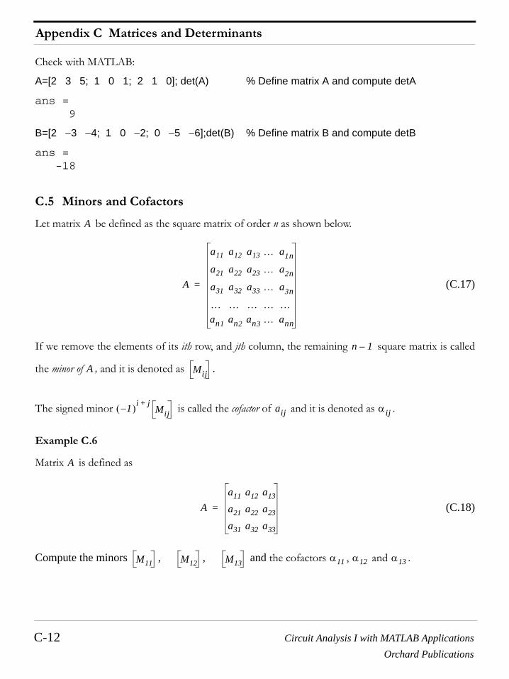
Appendix C Matrices and Determinants
C-12 Circuit Analysis I with MATLAB ApplicationsOrchard Publications
Check with MATLAB:
A=[2 3 5; 1 0 1; 2 1 0]; det(A) % Define matrix A and compute detA
ans = 9
B=[2 −3 −4; 1 0 −2; 0 −5 −6];det(B) % Define matrix B and compute detB
ans = -18
C.5 Minors and Cofactors
Let matrix be defined as the square matrix of order n as shown below.
(C.17)
If we remove the elements of its ith row, and jth column, the remaining square matrix is called
the minor of , and it is denoted as .
The signed minor is called the cofactor of and it is denoted as .
Example C.6
Matrix is defined as
(C.18)
Compute the minors , , and the cofactors , and .
A
A
a11 a12 a13 … a1n
a21 a22 a23 … a2n
a31 a32 a33 … a3n
… … … … …an1 an2 an3 … ann
=
n 1–
A Mij
1–( )i j+Mij aij αij
A
Aa11 a12 a13
a21 a22 a23
a31 a32 a33
=
M11 M12 M13 α11 α12 α13

Circuit Analysis I with MATLAB Applications C-13Orchard Publications
Minors and Cofactors
Solution:
and
The remaining minors
and cofactors
are defined similarly.
Example C.7
Compute the cofactors of matrix defined as
(C.19)
Solution:
(C.20)
(C.21)
(C.22)
(C.23)
(C.24)
M11a22 a23
a32 a33
= M12a21 a23
a31 a33
= M11a21 a22
a31 a32
=
α11 1–( )1 1+M11 M11 α12 1–( )1 2+
M12 M12 α13 M13 1–( )1 3+M13= =–= == =
M21 M22 M23 M31 M32 M33, , , , ,
α21 α22 α23 α31 α32 and α33, , , , ,
A
A1 2 3–
2 4– 21– 2 6–
=
α11 1–( )1 1+ 4– 22 6–
20= = α12 1–( )1 2+ 2 21– 6–
10= =
α13 1–( )1 3+ 2 4–
1– 20 α21 1–( )2 1+ 2 3–
2 6–6= == =
α22 1–( )2 2+ 1 3–
1– 6–9–= = α23 1–( )2 3+ 1 2
1– 24–= =
α31 1–( )3 1+ 2 3–
4– 28–= = α32 1–( )3 2+ 1 3–
2 28–= =,
α33 1–( )3 3+ 1 22 4–
8–= =

Appendix C Matrices and Determinants
C-14 Circuit Analysis I with MATLAB ApplicationsOrchard Publications
It is useful to remember that the signs of the cofactors follow the pattern
that is, the cofactors on the diagonals have the same sign as their minors.
Let be a square matrix of any size; the value of the determinant of is the sum of the productsobtained by multiplying each element of any row or any column by its cofactor.
Example C.8
Matrix is defined as
(C.25)
Compute the determinant of using the elements of the first row.
Solution:
Check with MATLAB:
A=[1 2 −3; 2 −4 2; −1 2 −6];det(A) % Define matrix A and compute detA
ans = 40
We must use the above procedure to find the determinant of a matrix of order 4 or higher. Thus, afourth-order determinant can first be expressed as the sum of the products of the elements of its firstrow by its cofactor as shown below.
+ − + − +− + − + −+ − + − +− + − + −+ − + − +
A A
A
A1 2 3–
2 4– 21– 2 6–
=
A
detA 1 4– 22 6–
= 2 2 21– 6–
3 2 4–
1– 2–– 1 20× 2 10–( )× 3 0×–– 40= =
A

Circuit Analysis I with MATLAB Applications C-15Orchard Publications
Minors and Cofactors
(C.26)
Determinants of order five or higher can be evaluated similarly.
Example C.9
Compute the value of the determinant of the matrix defined as
(C.27)
Solution:
Using the above procedure, we will multiply each element of the first column by its cofactor. Then,
Next, using the procedure of Example C.5 or Example C.8, we find
, , , and thus
We can verify our answer with MATLAB as follows:
A=[ 2 −1 0 −3; −1 1 0 −1; 4 0 3 −2; −3 0 0 1]; delta = det(A)
delta = -33
A
a11 a12 a13 a14
a21 a22 a23 a24
a31 a32 a33 a34
a41 a42 a43 a44
a11
a22 a23 a24
a32 a33 a34
a42 a43 a44
a21
a12 a13 a14
a32 a33 a34
a42 a43 a44
–
+a31
a12 a13 a14
a22 a23 a24
a42 a43 a44
a41
a12 a13 a14
a22 a23 a24
a32 a33 a34
–
= =
A
A
2 1– 0 3–
1– 1 0 1–
4 0 3 2–
3– 0 0 1
=
A=21 0 1–
0 3 2–
0 0 1
a[ ]
1–( )1– 0 3–
0 3 2–
0 0 1
–
b[ ]
+4
1– 0 3–
1 0 1–
0 0 1
c[ ]
3–( )1– 0 3–
1 0 1–
0 3 2–
–
d[ ]
⎧ ⎪ ⎪ ⎨ ⎪ ⎪ ⎩ ⎧ ⎪ ⎪ ⎪ ⎨ ⎪ ⎪ ⎪ ⎩ ⎧ ⎪ ⎪ ⎨ ⎪ ⎪ ⎩ ⎧ ⎪ ⎪ ⎪ ⎨ ⎪ ⎪ ⎪ ⎩
a[ ] 6= b[ ] 3–= c[ ] 0= d[ ] 36–=
detA a[ ] b[ ] c[ ] d[ ]+ + + 6 3– 0 36–+ 33–= = =

Appendix C Matrices and Determinants
C-16 Circuit Analysis I with MATLAB ApplicationsOrchard Publications
Some useful properties of determinants are given below.
Property 1: If all elements of one row or one column are zero, the determinant is zero. An example of this is thedeterminant of the cofactor above.
Property 2: If all the elements of one row or column are m times the corresponding elements of another row or col-umn, the determinant is zero. For example, if
(C.28)
then,
(C.29)
Here, is zero because the second column in is 2 times the first column.
Check with MATLAB:
A=[2 4 1; 3 6 1; 1 2 1];det(A)
ans = 0
Property 3: If two rows or two columns of a matrix are identical, the determinant is zero. This follows fromProperty 2 with .
C.6 Cramer’s Rule
Let us consider the systems of the three equations below
(C.30)
and let
c[ ]
A2 4 13 6 11 2 1
=
detA2 4 13 6 11 2 1
2 43 61 2
12 4 6 6 4–– 12–+ + 0= = =
detA A
m 1=
a11x a12y a13z+ + A=
a21x a22y a23z+ + B=
a31x a32y a33z+ + C=
∆a11 a12 a13
a21 a22 a23
a31 a32 a33
D1
A a11 a13
B a21 a23
C a31 a33
D2
a11 A a13
a21 B a23
a31 C a33
D3
a11 a12 Aa21 a22 Ba31 a32 C
====
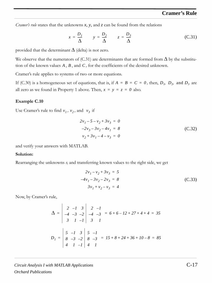
Circuit Analysis I with MATLAB Applications C-17Orchard Publications
Cramer’s Rule
Cramer’s rule states that the unknowns x, y, and z can be found from the relations
(C.31)
provided that the determinant ∆ (delta) is not zero.
We observe that the numerators of (C.31) are determinants that are formed from ∆ by the substitu-tion of the known values , , and , for the coefficients of the desired unknown.
Cramer’s rule applies to systems of two or more equations.
If (C.30) is a homogeneous set of equations, that is, if , then, areall zero as we found in Property 1 above. Then, also.
Example C.10
Use Cramer’s rule to find , , and if
(C.32)
and verify your answers with MATLAB.
Solution:
Rearranging the unknowns v, and transferring known values to the right side, we get
(C.33)
Now, by Cramer’s rule,
xD1
∆------= y
D2
∆------= z
D3
∆------=
A B C
A B C 0= = = D1 D2 and D3, ,
x y z 0= = =
v1 v2 v3
2v1 5– v2– 3v3+ 0=
2v3 3v2 4v1––– 8=
v2 3v1 4– v3–+ 0=
2v1 v2– 3v3+ 5=
4v1 3v2 2v3––– 8=
3v1 v2 v3–+ 4=
∆2 1– 34– 3– 2–
3 1 1–
2 1–
4– 3–
3 1
6 6 12– 27 4 4+ + + + 35= = =
D1
5 1– 38 3– 2–
4 1 1–
5 1–
8 3–
4 1
15 8 24 36 10 8–+ + + + 85= = =

Appendix C Matrices and Determinants
C-18 Circuit Analysis I with MATLAB ApplicationsOrchard Publications
Then, using (C.31) we get
(C.34)
We will verify with MATLAB as follows.
% The following code will compute and display the values of v1, v2 and v3.format rat % Express answers in ratio formB=[2 −1 3; −4 −3 −2; 3 1 −1]; % The elements of the determinant D of matrix Bdelta=det(B); % Compute the determinant D of matrix Bd1=[5 -1 3; 8 -3 -2; 4 1 -1]; % The elements of D1detd1=det(d1); % Compute the determinant of D1d2=[2 5 3; -4 8 -2; 3 4 -1]; % The elements of D2detd2=det(d2); % Compute the determinant of D2d3=[2 -1 5; -4 -3 8; 3 1 4]; % The elements of D3detd3=det(d3); % Compute he determinant of D3v1=detd1/delta; % Compute the value of v1v2=detd2/delta; % Compute the value of v2v3=detd3/delta; % Compute the value of v3%disp('v1=');disp(v1); % Display the value of v1disp('v2=');disp(v2); % Display the value of v2disp('v3=');disp(v3); % Display the value of v3
v1= 17/7v2= -34/7 v3= -11/7
These are the same values as in (C.34)
D2
2 5 34– 8 2–
3 4 1–
2 54– 83 4
16– 30– 48– 72– 16 20–+ 170–= = =
D3
2 1– 54– 3– 83 1 4
2 1–
4– 3–
3 1
24– 24– 20– 45 16– 16–+ 55–= = =
x1D1
∆------ 85
35------ 17
7------= = = x2
D2
∆------ 170
35---------– 34
7------–= = = x3
D3
∆------ 55
35------– 11
7------–= = =

Circuit Analysis I with MATLAB Applications C-19Orchard Publications
Gaussian Elimination Method
C.7 Gaussian Elimination Method
We can find the unknowns in a system of two or more equations also by the Gaussian eliminationmethod. With this method, the objective is to eliminate one unknown at a time. This can be done bymultiplying the terms of any of the equations of the system by a number such that we can add (orsubtract) this equation to another equation in the system so that one of the unknowns will be elimi-nated. Then, by substitution to another equation with two unknowns, we can find the secondunknown. Subsequently, substitution of the two values found can be made into an equation withthree unknowns from which we can find the value of the third unknown. This procedure is repeateduntil all unknowns are found. This method is best illustrated with the following example which con-sists of the same equations as the previous example.
Example C.11
Use the Gaussian elimination method to find , , and of the system of equations
(C.35)
Solution:
As a first step, we add the first equation of (C.35) with the third to eliminate the unknown v2 and weobtain the following equation.
(C.36)
Next, we multiply the third equation of (C.35) by 3, and we add it with the second to eliminate .Then, we obtain the following equation.
(C.37)
Subtraction of (C.37) from (C.36) yields
(C.38)
Now, we can find the unknown from either (C.36) or (C.37). By substitution of (C.38) into (C.36)we get
(C.39)
Finally, we can find the last unknown from any of the three equations of (C.35). By substitutioninto the first equation we get
v1 v2 v3
2v1 v2– 3v3+ 5=
4v1 3v2 2v3––– 8=
3v1 v2 v3–+ 4=
5v1 2v3+ 9=
v2
5v1 5v3– 20=
7v3 11 or v3117------–=–=
v1
5v1 2 117
------–⎝ ⎠⎛ ⎞⋅+ 9 or v1
177
------==
v2

Appendix C Matrices and Determinants
C-20 Circuit Analysis I with MATLAB ApplicationsOrchard Publications
(C.40)
These are the same values as those we found in Example C.10.
The Gaussian elimination method works well if the coefficients of the unknowns are small integers,as in Example C.11. However, it becomes impractical if the coefficients are large or fractional num-bers.
C.8 The Adjoint of a Matrix
Let us assume that is an n square matrix and is the cofactor of . Then the adjoint of ,
denoted as , is defined as the n square matrix below.
(C.41)
We observe that the cofactors of the elements of the ith row (column) of are the elements of theith column (row) of .
Example C.12
Compute if Matrix is defined as
(C.42)
Solution:
v2 2v1 3v3 5–+ 347
------ 337
------– 357
------– 347
------–= = =
A αij aij A
adjA
adjA
α11 α21 α31 … αn1
α12 α22 α32 … αn2
α13 α23 α33 … αn3
… … … … …α1n α2n α3n … αnn
=
AadjA
adjA A
A1 2 31 3 41 4 3
=
adjA
3 44 3
2 34 3
– 2 33 4
1 41 3
– 1 31 3
2 33 4
–
1 31 4
1 21 4
– 1 21 3
7– 6 1–
1 0 1–
1 2– 1
= =

Circuit Analysis I with MATLAB Applications C-21Orchard Publications
Singular and Non-Singular Matrices
C.9 Singular and Non-Singular Matrices
An n square matrix is called singular if ; if , is called non-singular.
Example C.13
Matrix is defined as
(C.43)
Determine whether this matrix is singular or non-singular.
Solution:
Therefore, matrix is singular.
C.10 The Inverse of a Matrix
If and are n square matrices such that , where is the identity matrix, is called
the inverse of , denoted as , and likewise, is called the inverse of , that is,
If a matrix is non-singular, we can compute its inverse from the relation
(C.44)
Example C.14
Matrix is defined as
(C.45)
Compute its inverse, that is, find
A detA 0= detA 0≠ A
A
A1 2 32 3 43 5 7
=
detA1 2 32 3 43 5 7
1 22 33 5
21 24 30 27– 20– 28–+ + 0= = =
A
A B AB BA I= = I B
A B A 1–= A B A B 1–=
A A 1–
A 1– 1detA------------adjA=
A
A1 2 31 3 41 4 3
=
A 1–

Appendix C Matrices and Determinants
C-22 Circuit Analysis I with MATLAB ApplicationsOrchard Publications
Solution:
Here, , and since this is a non-zero value, it is possible to com-pute the inverse of using (C.44).
From Example C.12,
Then,
(C.46)
Check with MATLAB:
A=[1 2 3; 1 3 4; 1 4 3], invA=inv(A) % Define matrix A and compute its inverse
A = 1 2 3 1 3 4 1 4 3
invA = 3.5000 -3.0000 0.5000 -0.5000 0 0.5000 -0.5000 1.0000 -0.5000
Multiplication of a matrix by its inverse produces the identity matrix , that is,
(C.47)
Example C.15
Prove the validity of (C.47) for the Matrix defined as
Proof:
detA 9 8 12 9– 16– 6–+ + 2–= =
A
adjA7– 6 1–
1 0 1–
1 2– 1
=
A 1– 1detA------------adjA 1
2–------
7– 6 1–
1 0 1–
1 2– 1
3.5 3– 0.50.5– 0 0.50.5– 1 0.5–
= = =
A A 1– I
AA 1– I or A 1– A I ==
A
A 4 32 2
=
detA 8 6– 2 and adjA 2 3–
2– 4== =

Circuit Analysis I with MATLAB Applications C-23Orchard Publications
Solution of Simultaneous Equations with Matrices
Then,
and
C.11 Solution of Simultaneous Equations with Matrices
Consider the relation
(C.48)
where and are matrices whose elements are known, and is a matrix (a column vector) whoseelements are the unknowns. We assume that and are conformable for multiplication. Multipli-
cation of both sides of (C.48) by yields:
(C.49)
or
(C.50)
Therefore, we can use (C.50) to solve any set of simultaneous equations that have solutions. We willrefer to this method as the inverse matrix method of solution of simultaneous equations.
Example C.16
For the system of the equations
(C.51)
compute the unknowns using the inverse matrix method.
Solution:
In matrix form, the given set of equations is where
A 1– 1detA------------adjA 1
2--- 2 3–
2– 41 3– 2⁄1– 2
= = =
AA 1– 4 32 2
1 3– 2⁄1– 2
4 3– 6– 6+
2 2– 3– 4+
1 00 1
I= = = =
AX B=
A B XA X
A 1–
A 1– AX A 1– B IX A 1– B = = =
X=A 1– B
2x1 3x2 x3+ + 9=
x1 2x2 3x3+ + 6=
3x1 x2 2x3+ + 8=⎩ ⎭⎪ ⎪⎨ ⎬⎪ ⎪⎧ ⎫
x1 x2 and x3, ,
AX B=
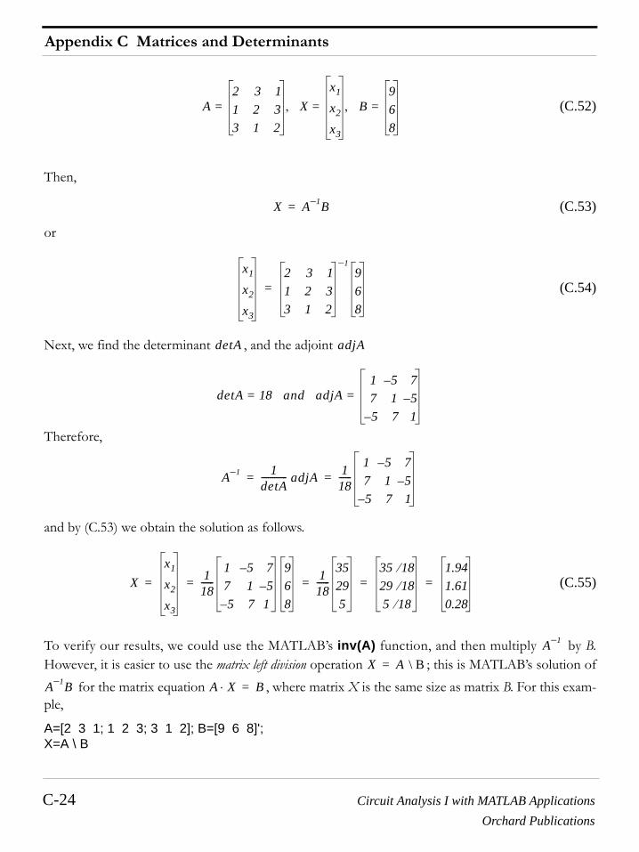
Appendix C Matrices and Determinants
C-24 Circuit Analysis I with MATLAB ApplicationsOrchard Publications
(C.52)
Then,
(C.53)
or
(C.54)
Next, we find the determinant , and the adjoint
Therefore,
and by (C.53) we obtain the solution as follows.
(C.55)
To verify our results, we could use the MATLAB’s inv(A) function, and then multiply by B.However, it is easier to use the matrix left division operation ; this is MATLAB’s solution of
for the matrix equation , where matrix X is the same size as matrix B. For this exam-ple,
A=[2 3 1; 1 2 3; 3 1 2]; B=[9 6 8]';X=A \ B
A2 3 11 2 33 1 2
= Xx1
x2
x3
= B968
=, ,
X A 1– B=
x1
x2
x3
2 3 11 2 33 1 2
1–968
=
detA adjA
detA 18= and adjA1 5– 77 1 5–
5– 7 1
=
A 1– 1detA------------ adjA 1
18------
1 5– 77 1 5–
5– 7 1
= =
Xx1
x2
x3
118------
1 5– 77 1 5–
5– 7 1
968
118------
35295
35 18⁄29 18⁄5 18⁄
1.941.610.28
= = = = =
A 1–
X A \ B=
A 1– B A X⋅ B=
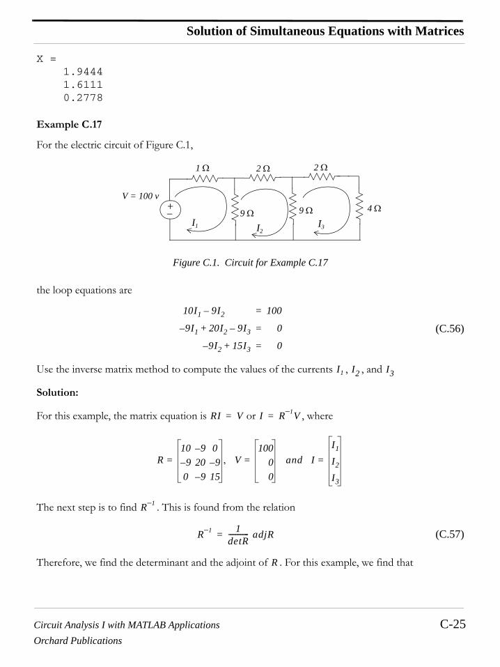
Circuit Analysis I with MATLAB Applications C-25Orchard Publications
Solution of Simultaneous Equations with Matrices
X = 1.9444 1.6111 0.2778
Example C.17
For the electric circuit of Figure C.1,
Figure C.1. Circuit for Example C.17
the loop equations are
(C.56)
Use the inverse matrix method to compute the values of the currents , , and
Solution:
For this example, the matrix equation is or , where
The next step is to find . This is found from the relation
(C.57)
Therefore, we find the determinant and the adjoint of . For this example, we find that
+−
V = 100 v
9 Ω 9 Ω 4 Ω
2 Ω2 Ω1 Ω
I1 I3I2
10I1 9I2– 100=
9I1 20I2 9I3–+– 0=
9I2 15I3+– 0=
I1 I2 I3
RI V = I R 1– V=
R10 9– 0
9– 20 9–
0 9– 15
= V100
00
and II1
I2
I3
==,
R 1–
R 1– 1detR------------ adjR=
R
Appendix C Matrices and Determinants
C-26 Circuit Analysis I with MATLAB ApplicationsOrchard Publications
(C.58)
Then,
and
Check with MATLAB:
R=[10 −9 0; −9 20 −9; 0 −9 15]; V=[100 0 0]'; I=R\V
I = 22.4615 13.8462 8.3077
We can also use subscripts to address the individual elements of the matrix. Accordingly, the abovecode could also have been written as:
R(1,1)=10; R(1,2)=-9; % No need to make entry for A(1,3) since it is zero.R(2,1)=-9; R(2,2)=20; R(2,3)=-9; R(3,2)=-9; R(3,3)=15; V=[100 0 0]'; I=R\V
I = 22.4615 13.8462 8.3077
Spreadsheets also have the capability of solving simultaneous equations using the inverse matrixmethod. For instance, we can use Microsoft Excel’s MINVERSE (Matrix Inversion) and MMULT(Matrix Multiplication) functions, to obtain the values of the three currents in Example C.17.
The procedure is as follows:
1. We start with a blank spreadsheet and in a block of cells, say B3:D5, we enter the elements ofmatrix R as shown in Figure C.2. Then, we enter the elements of matrix in G3:G5.
detR 975= adjR219 135 81135 150 9081 90 119
=,
R 1– 1detR------------adjR 1
975---------
219 135 81135 150 9081 90 119
= =
II1
I2
I3
1975---------
219 135 81135 150 9081 90 119
10000
100975---------
21913581
22.4613.858.31
= = = =
V

Circuit Analysis I with MATLAB Applications C-27Orchard Publications
Solution of Simultaneous Equations with Matrices
2. Next, we compute and display the inverse of R, that is, . We choose B7:D9 for the elementsof this inverted matrix. We format this block for number display with three decimal places. Withthis range highlighted and making sure that the cell marker is in B7, we type the formula
=MININVERSE(B3:D5)
and we press the Crtl-Shift-Enter keys simultaneously.
We observe that appears in these cells.
3. Now, we choose the block of cells G7:G9 for the values of the current I. As before, we highlightthem, and with the cell marker positioned in G7, we type the formula
=MMULT(B7:D9,G3:G5)
and we press the Crtl-Shift-Enter keys simultaneously. The values of I then appear in G7:G9.
Figure C.2. Solution of Example C.17 with a spreadsheet
Example C.18
For the phasor circuit of Figure C.18
Figure C.3. Circuit for Example C.18
R 1–
R 1–
12345678910
A B C D E F G HSpreadsheet for Matrix Inversion and Matrix Multiplication
10 -9 0 100R= -9 20 -9 V= 0
0 -9 15 0
0.225 0.138 0.083 22.462R-1= 0.138 0.154 0.092 I= 13.846
0.083 0.092 0.122 8.3077
+
−
R1
85 Ω
50 ΩR2
C
L
R3 = 100 Ω
IX
VS
−j100 Ω
j200 Ω
170∠0°
V1 V2

Appendix C Matrices and Determinants
C-28 Circuit Analysis I with MATLAB ApplicationsOrchard Publications
the current can be found from the relation
(C.59)
and the voltages V1 and V2 can be computed from the nodal equations
(C.60)
and
(C.61)
Compute, and express the current in both rectangular and polar forms by first simplifying liketerms, collecting, and then writing the above relations in matrix form as , where
, , and
Solution:
The Y matrix elements are the coefficients of and . Simplifying and rearranging the nodalequations of (C.60) and (C.61), we get
(C.62)
Next, we write (C.62) in matrix form as
(C.63)
where the matrices , , and are as indicated.
We will use MATLAB to compute the voltages and , and to do all other computations. Thecode is shown below.
Y=[0.0218−0.005j −0.01; −0.01 0.03+0.01j]; I=[2; 1.7j]; V=Y\I;% Define Y, I, and find Vfprintf('\n'); % Insert a line disp('V1 = '); disp(V(1)); disp('V2 = '); disp(V(2)); % Display values of V1 and V2
IX
IXV1 V2–
R3------------------=
V1 170 0°∠–
85-------------------------------
V1 V2–
100------------------
V1 0–
j200---------------+ + 0=
V2 170 0°∠–
j100–-------------------------------
V2 V1–
100------------------
V2 0–
50---------------+ + 0=
Ix
YV I=
Y Admit cetan= V Voltage= I Current=
V1 V2
0.0218 j0.005–( )V1 0.01V2– 2=
0.01– V1 0.03 j0.01+( )V2+ j1.7=
0.0218 j0.005– 0.01–
0.01– 0.03 j0.01+
Y
V1
V2
V
2j1.7
I
=
⎧ ⎪ ⎪ ⎪ ⎪ ⎪ ⎨ ⎪ ⎪ ⎪ ⎪ ⎪ ⎩ ⎧ ⎨ ⎩ ⎧ ⎨ ⎩
Y V I
V1 V2

Circuit Analysis I with MATLAB Applications C-29Orchard Publications
Solution of Simultaneous Equations with Matrices
V1 = 1.0490e+002 + 4.9448e+001i
V2 = 53.4162 + 55.3439i
Next, we find from
R3=100; IX=(V(1)−V(2))/R3 % Compute the value of IX
IX = 0.5149- 0.0590i
This is the rectangular form of . For the polar form we use
magIX=abs(IX) % Compute the magnitude of IX
magIX = 0.5183
thetaIX=angle(IX)*180/pi % Compute angle theta in degrees
thetaIX = -6.5326
Therefore, in polar form
Spreadsheets have limited capabilities with complex numbers, and thus we cannot use them to com-pute matrices that include complex numbers in their elements as in Example C.18
IX
IX
IX 0.518 6.53°–∠=

Appendix C Matrices and Determinants
C-30 Circuit Analysis I with MATLAB ApplicationsOrchard Publications
C.12 Exercises
For Problems 1 through 3 below, the matrices , , , and are defined as:
1. Perform the following computations, if possible. Verify your answers with MATLAB.
a. b. c. d.
e. f. g. h.
2. Perform the following computations, if possible. Verify your answers with MATLAB.
a. b. c. d.
e. f. g. h.
3. Perform the following computations, if possible. Verify your answers with MATLAB.
a. b. c. d.
e. f.
4. Solve the following systems of equations using Cramer’s rule. Verify your answers with MATLAB.
a. b.
5. Repeat Exercise 4 using the Gaussian elimination method.
6. Solve the following systems of equations using the inverse matrix method. Verify your answerswith MATLAB.
a. b.
A B C D
A1 1– 4–
5 7 2–
3 5– 6
= B5 9 3–
2– 8 27 4– 6
= C=4 63– 85 2–
D 1 2– 33– 6 4–
=
A B+ A C+ B D+ C D+
A B– A C– B D– C D–
A B⋅ A C⋅ B D⋅ C D⋅
B A⋅ C A⋅ D A⋅ D· C⋅
detA detB detC detD
det A B⋅( ) det A C⋅( )
x1 2x2 x3+– 4–=
2x– 1 3x2 x3+ + 9=
3x1 4x2 5x3–+ 0=
x1– 2x2 3x3– 5x4+ + 14=
x1 3x2 2x3 x4–+ + 9=
3x1 3– x2 2x3 4x4+ + 19=
4x1 2x2 5x3 x4+ + + 27=
1 3 43 1 2–
2 3 5
x1
x2
x3
⋅3–
2–
0
=
2 4 3 2–
2 4– 1 31– 3 4– 22 2– 2 1
x1
x2
x3
x4
⋅
11014–
7
=

IndexSymbols and Numerics complex excitation function 6-3, 6-21 delta function
complex number(s) defined 10-8% (percent) symbol in MATLAB A-2 addition B-2 sampling property 10-83-dB down 4-4 conjugate A-4, B-3 sifting property 10-9
defined A-3, B-2 demos in MATLAB A-2A division B-4 dependent source(s)
exponential form B-5 current 1-10, 3-41abs(z) in MATLAB A-25 multiplication B-3 voltage 1-10, 3-41admittance 6-17 polar form B-5 determinant C-9ampere 1-1, 1-19 rectangular form B-5 device(s)ampere capacity of wires 2-30 subtraction B-2 active 1-12, 1-20amplifier 4-1, 4-32 complex power 8-16, 8-17 passive 1-12, 1-20 buffer 4-20 conductance 2-2 dielectric 5-17, 5-30 unity gain 4-12, 4-20 conj(A), conj(x) in MATLAB C-8 differential input amplifier 4-5analog-to-digital converter 8-28, 8-32 conjugate of a complex number B-3 digital filter 7-21angle(z) in MATLAB A-25 conv(a,b) in MATLAB A-6 diode(s) 1-10attenuation 4-13, 4-33 conversion factors 1-16 Dirac function 10-9attenuator 4-1 conductor sizes for interior wiring 2-33 direct current 1-4average value 8-2, 8-30 coulomb 1-1, 1-18 discontinuous function 10-1axis in MATLAB A-17, A-18, A-23 Cramer’s rule 3-2, C-16, C-17 disp(A) in MATLAB 7-19, A-32
critical frequency 4-13, 4-33 display formats in MATLAB A-31B current 1-1 division in MATLAB A-22
current division expressions 2-25 dot multiplication operator in MATLAB A-22bandwidth 4-4 current flow driving functions 6-1box in MATLAB A-13 conventional 1-2 duality 6-19, 6-24branch 2-5 electron 1-2
current gain 4-2 EC current limiting devices 2-2
current ratings for editor window in MATLAB A-1capacitance 5-17 electronic equipment 2-30 editor/debugger in MATLAB A-1, A-2capacitance combinations 5-25 current source effective (RMS) value of sinusoids 8-5capacitor(s) 1-12, 1-20, 5-17 combinations 2-17, 2-18 effective values 8-3 in parallel 5-27 ideal 1-11 efficiency 3-47 in series 5-26 independent 1-11 eight-to-three line encoder 8-28chemical processes 1-17, 1-20 practical 3-21 electric field 5-17, 5-18, 5-30circuit(s) cutoff frequency electric filters - see filters defined 1-12, 1-20 band-elimination filter 4-15 energy dissipated in a resistor 2-4 analysis with loop equations 3-8 band-pass filter 4-15 energy stored in a capacitor 5-22 analysis with mesh equations 3-8 high-pass filter 4-14 energy stored in an inductor 5-12 analysis with nodal equations 3-1 low-pass filter 4-13 eps in MATLAB A-23, A-28 with non-linear devices 3-45 lower 4-4 Euler’s identities B-4clc in MATLAB A-2 upper 4-4 excitations 6-1clear in MATLAB A-2 exit in MATLAB A-2combined mesh 3-18 D exponential form of complex numbers B-5combined node 3-6 exponentiation in MATLAB A-22command screen in MATLAB A-1 data points in MATLAB A-15 eye(n) in MATLAB C-7command window in MATLAB A-1 DC (Direct Current) 1-4 eye(size(A)) in MATLAB C-7commas in MATLAB A-8 decibel 4-2, A-13comment line in MATLAB A-2 deconv(c,d) in MATLAB A-6, A-7 Fcomparators 8-28 default color in MATLAB A-16complementary function 9-1 default in MATLAB A-13 Farad 5-18, 5-30complete response 10-16 default line in MATLAB A-16 Faraday’s law ofcomplex conjugate A-4, B-3 default marker in MATLAB A-16 electromagnetic induction 5-2

feedback 4-4 imaginary M negative 4-5 axis B-2 positive 4-5 number B-2 magnetic field 5-1, 5-17, 5-29figure window in MATLAB A-14 impedance 6-14 magnetic flux 5-2, 5-29filter inductance 5-2 matrix, matrices active 4-13 inductive adjoint C-20 all-pass 7-20 reactance 6-15, 6-23 cofactor of C-12 analog 7-21 susceptance 6-18, 6-23 conformable for addition C-2 band-elimination 4-15, 4-33, 7-20 inductor(s) conformable for multiplication C-4 band-pass 4-14, 4-33, 7-20 defined 1-12, 1-20, 5-2 congugate of C-8 band-rejection 4-15, 4-33, 7-20 in parallel 5-16 defined C-1 band-stop 4-15, 4-33, 7-20 in series 5-15 diagonal of C-1, C-6 high-pass 4-14, 4-33, 7-20, 7-23 initial condition 5-3 Hermitian C-9 low-pass 4-13, 4-33, 7-20, 7-21 initial rate of decay 9-3, 9-11 identity C-6 passive 4-13, 7-21 instantaneous values 2-1 inverse of C-21 phase shift 7-21 int(f,a,b) in MATLAB 1-7 left division in MATLAB C-24 RC high-pass 7-23 International System of Units 1-13 lower triangular C-6 RC low-pass 7-21 minor of C-12 stop-band 4-15, 4-33, 7-20 J multiplication using MATLAB A-20flash converter 8-28 non-singular C-21flux linkage 5-2, 5-29 j operator B-1 singular C-21fmax(f,x1,x2) in MATLAB A-28 scalar C-6fmin(f,x1,x2) in MATLAB A-28, A-30 K skew-Hermitian C-9forced response 6-4, 10-16, 10-23 skew-symmetric C-9format command in MATLAB A-31 KCL 2-6 square C-1format in MATLAB A-31 Kirchhoff’s Current Law 2-6 symmetric C-8fplot in MATLAB A-28 Kirchhoff’s Voltage Law 2-7 theory 3-2fplot(fcn,lims) KVL 2-7 trace of C-2 in MATLAB A-28, A-29 transpose C-7fprintf(format,array) L upper triangular C-5 in MATLAB 7-19, A-32 zero C-2frequency response A-13 left-hand rule 5-1 maximum powerfrequency-domain to time-domain lims = in MATLAB A-28 transfer theorem 3-38, 7-35 transformation 6-6, 6-22 linear mechanical forms of energy 1-17, 1-20full-wave rectification circuit 3-40 meshfunction file in MATLAB A-26, A-28 devices 1-10 combined 3-18fzero(f,x) in MATLAB A-28, A-30 factor A-9 defined 2-6
inductor 5-2 equations 2-10, 3-1, 5-28, 7-5 G passive element 3-39 generalized 3-18
linearity 3-39 mesh(x,y,z) in MATLAB A-18Gaussian elimination method C-19 lines of magnetic flux 5-1, 5-29 meshgrid(x,y) in MATLAB A-18grid in MATLAB A-13 linspace(values) in MATLAB A-14 metric system 1-13, 1-20ground ln (natural log) A-13 m-file in MATLAB A-1, A-26 defined 2-1, 2-15 load mho 2-2 virtual 4-17 capacitive 8-15, 8-31 Military Standards 2-27gtext(‘string’) in MATLAB A-14 inductive 8-15, 8-31 MINVERSE in Excel C-26
lighting 2-34 MMULT in Excel C-26, C-27H resistive 8-10 multiplication of complex numbers B-3
log (common log) A-13 multiplication in MATLAB A-20, A-21half-power points 4-4 log(x) in MATLAB A-13 multirange ammeter/milliammeter 8-24half-wave rectification 8-3 log10(x) in MATLAB A-13Heavyside function 10-9 log2(x) in MATLAB A-13 NHenry 5-3, 5-29 loglog(x,y) in MATLAB A-13
loop NaN in MATLAB A-28I defined 2-5 National Electric Code (NEC) 2-30
equations 3-1, 3-13 natural responseimag(z) in MATLAB A-25 circuits with single 2-10 9-1, 9-10, 10-16, 10-23

NEC 2-30 complex 8-16, 8-17 series connection 2-8, 2-16, 2-17negative charge 5-18 gain 4-2 short circuit 2-2network in a capacitor 5-22 SI Derived Units 1-17 active 1-12, 1-20 in an inductor 5-11 siemens 2-2 passive 1-12, 1-20 in a resistor 2-3, 2-4, 2-28 signal 4-1, 4-32 topology 3-1 instantaneous 8-3 single ended output amplifier 4-5newton 1-1, 1-18 power factor 8-10 single node-pair parallel circuit 2-14nodal analysis 2-14, 3-1, 7-1 defined 8-10 slope converter 8-28node lagging 8-15 solar energy 1-17, 1-20 combined 3-6 leading 8-15 sources of energy 1-17, 1-20 defined 2-5 power factor correction 8-18 standard prefixes 1-14 generalized 3-6 power triangle 8-16 Standards for Electrical and equations 2-14, 3-1, 5-28, 7-1 prefixes 1-14, 1-15 Electronic Devices 2-26 non-reference 3-1 principle of superposition 3-41 steady-state conditions 5-12 reference 3-1 string in MATLAB A-18non-linear devices 1-10 Q subplot(m,n,p) in MATLAB A-19Norton’s theorem 3-35, 7-8 substitution method of solving a systemnuclear energy 1-17, 1-20 quad in MATLAB 1-6, 1-7 of simultaneous equations 3-2
quad(‘f’,a,b,tol) in MATLAB 1-7 supermesh 3-18O quad8 in MATLAB 1-7 supernode 3-6
quadratic factors A-9 superposition principle 3-41, 7-7Ohm 2-1 quit in MATLAB A-2 susceptance 6-18, 6-23Ohm’s law 2-1 capacitive 6-18, 6-23Ohm’s law for AC circuits 6-15 R inductive 6-18, 6-23Ohmmeter 8-26 parallel type 8-26 rational polynomials A-8 T series type 8-26 reactance shunt type 8-26 capacitive 6-15, 6-23 temperature scales equivalents 1-16op amp 4-5 inductive 6-15, 6-23 text(x,y,’string’) in MATLAB A-14 inverting mode 4-6 real text(x,y,z,’string’) in MATLAB A-18 non-inverting mode 4-9 axis B-2 Thevenin’s theorem 3-24, 7-8open circuit 2-2 number B-2 time constant 9-3, 9-11, 10-18, 10-24operational amplifier - see op amp real(z) in MATLAB A-25 time-domain to frequency-domain
regulation 3-49 transformation 6-6, 6-21P resistance time-window converter 8-28
defined 2-1 title(‘string’) in MATLAB A-13parallel connection 2-8, 2-17, 2-18 input 4-28 total response 10-16particular solution 6-4 output 4-28 tracking converter 8-28passive sign convention 1-8, 1-19 resistive network 8-28 transient response 9-1periodic functions of time 8-1 resistors 1-12, 2-2 transistors 1-10phasor analysis in amplifier circuits 7-12 color code 2-27 trivial solution 9-2phasor diagram 7-15 failure rate 2-27 two-terminal device 1-4, 1-19plot(x,y) in MATLAB A-10, A-12, A-16 shunt 8-21plot3(x,y,z) in MATLAB A-16 tolerance 2-27 Upolar plot in MATLAB A-25 response 6-1, 6-21polar(theta,r) in MATLAB A-25 right-hand rule 5-1 unit impulse function 10-8, 10-32poly(r) in MATLAB A-4, A-5 RMS value of sinusoids 8-5 unit ramp function 10-6, 10-32polyder(p) in MATLAB A-6, A-8 RMS values of sinusoids with unit step function 10-1, 10-31polynomial construction from different frequencies 8-7 known roots in MATLAB A-4 roots(p) in MATLAB A-3, A-8, A-9 Vpolyval(p,x) in MATLAB A-6 round(n) in MATLAB A-25potential difference 1-4 virtual ground 4-17power S volt 1-5, 1-19 absorbed 1-8, 1-19 voltage average 8-9, 8-14 script file in MATLAB A-26 defined 1-4 in capacitive loads 8-11 semicolons in MATLAB A-8 dividers 2-2 in inductive loads 8-11 semilogx(x,y) in MATLAB A-13 division expressions 2-23 in a resistive loads 8-10 semilogy(x,y) in MATLAB A-13 drop 1-5

follower 4-20 gain 4-2 instantaneous 1-5 rise 1-5voltage source combinations 2-16, 2-17 ideal 1-11 independent 1-11 practical 3-20voltmeter 8-24
W
watt 1-8watt-hour meter 8-28wattmeter 8-28weber 5-1, 5-29Wheatstone bridge 8-27, 8-32
X
xlabel(‘string’) in MATLAB A-13
Y
ylabel(‘string’) in MATLAB A-13
Z
zero potential 2-15