Effect of strain on low-loss electron energy loss spectra of group
8
Effect of strain on low-loss electron energy loss spectra of group III-nitrides Justinas Palisaitis, Ching-Lien Hsiao, Muhammad Junaid, Jens Birch, Lars Hultman and Per O.Å. Persson Linköping University Post Print N.B.: When citing this work, cite the original article. Original Publication: Justinas Palisaitis, Ching-Lien Hsiao, Muhammad Junaid, Jens Birch, Lars Hultman and Per O.Å. Persson, Effect of strain on low-loss electron energy loss spectra of group III-nitrides, 2011, Physical Review B. Condensed Matter and Materials Physics, (84), 24, 245301. http://dx.doi.org/10.1103/PhysRevB.84.245301 Copyright: American Physical Society http://www.aps.org/ Postprint available at: Linköping University Electronic Press http://urn.kb.se/resolve?urn=urn:nbn:se:liu:diva-67981
Transcript of Effect of strain on low-loss electron energy loss spectra of group

Effect of strain on low-loss electron energy loss
spectra of group III-nitrides
Justinas Palisaitis, Ching-Lien Hsiao, Muhammad Junaid, Jens Birch,
Lars Hultman and Per O.Å. Persson
Linköping University Post Print
N.B.: When citing this work, cite the original article.
Original Publication:
Justinas Palisaitis, Ching-Lien Hsiao, Muhammad Junaid, Jens Birch, Lars Hultman and Per
O.Å. Persson, Effect of strain on low-loss electron energy loss spectra of group III-nitrides,
2011, Physical Review B. Condensed Matter and Materials Physics, (84), 24, 245301.
http://dx.doi.org/10.1103/PhysRevB.84.245301
Copyright: American Physical Society
http://www.aps.org/
Postprint available at: Linköping University Electronic Press
http://urn.kb.se/resolve?urn=urn:nbn:se:liu:diva-67981

PHYSICAL REVIEW B 84, 245301 (2011)
Effect of strain on low-loss electron energy loss spectra of group-III nitrides
J. Palisaitis,* C.-L. Hsiao, M. Junaid, J. Birch, L. Hultman, and P. O. A. PerssonThin Film Physics Division, Department of Physics, Chemistry, and Biology (IFM), Linkoping University, SE-58183, Linkoping, Sweden
(Received 17 May 2011; revised manuscript received 8 November 2011; published 7 December 2011)
Thin films of AlN experiencing different strain states were investigated with a scanning transmission electronmicroscope (STEM) by low-loss electron energy loss spectroscopy (EELS). The results conclude that the low-lossproperties and in particular, the plasmon peak position is shifted as a direct consequence of the inherent strainof the sample. The results reveal that strain, even minor levels, can be measured by STEM-EELS. These resultswere further corroborated by full potential calculations and expanded to include the similar III nitrides GaN andInN. It is found that a unit-cell volume change of 1% results in a bulk plasmon peak shift of 0.159, 0.168, and0.079 eV for AlN, GaN, and InN, respectively, according to simulations. The AlN peak shift was experimentallycorroborated with a corresponding peak shift of 0.156 eV. The unit-cell volume is used here since it is foundthat regardless of in- and out-of-plane lattice augmentation, the low-loss properties appear near identical forconstant volume. These results have an impact on the interpretation of the plasmon energy and its applicabilityfor determining and separating stress and composition. It is found that while the bulk plasmon energy can beused as a measure of the composition in a group-III nitride alloy for relaxed structures, the presence of strainsignificantly affects such a measurement. The strain is found to have a lower impact on the peak shift for Al1-xInxN(∼3% compositional error per 1% volume change) and In1-xGaxN alloys compared to significant variations forAl1-xGaxN (16% compositional error for 1% volume change). Hence a key understanding in low-loss studies ofIII nitrides is that strain and composition are coupled and affect one another.
DOI: 10.1103/PhysRevB.84.245301 PACS number(s): 79.20.Uv, 71.45.Gm, 68.60.Bs, 81.05.Ea
I. INTRODUCTION
Group-III nitride semiconductor alloys attract interest dueto promising applications for optoelectronic and electronicdevices due to unique physical properties and engineeringcapabilities.1 At the same time, modern electronic devicesare increasingly employing structures which are dimensionedon the nanoscale,2 such as optical devices based on quantumwells. As the structures are shrinking, the impact of strain,which appears when a material of a given structure, specificcomposition, and lattice parameters is adapting to a secondmaterial, has a significant impact on device characteristics.This is commonly used to increase performance, e.g., instrained SiGe layer devices.3,4 Device performance is affectednot only by strain in the active layers, but also by thecomposition of the layer. To achieve a thorough understandingof the device performance, one should seek to separate andidentify the impact of both strain and compositional variations,even on the nanoscale. However, the composition affects thelattice parameter, which is also affected by strain. Whilestrain and composition can commonly be measured by x-raydiffraction (XRD) or Raman spectroscopy, the two compo-nents are not easily separated. Decoupling of compositionaland strain effects on the macroscopic level can be achieved bycombining XRD with Rutherford backscattering spectroscopy(RBS).5 However, for performing strain and compositionalinvestigations on the nanometer scale (e.g., in an individualquantum well), a superior spatial resolution is required and canbe achieved in the scanning transmission electron microscope(STEM).
Various methods have been employed in the STEM toobtain a measure of strain, such as the geometric phase analysis(GPA)6 and peak pairs analysis (PPA).7 Furthermore, strainhas been investigated by convergent-beam electron diffraction(CBED)8 and nanobeam electron diffraction (NBD),9 as well
as by nanoscale holographic interferometry.10 The abilityto separate the information into strain and composition onnanoscale proves to be challenging. As an example, GPA andPPA are based on evaluation of the crystal lattice spacing,which regretfully depends on both strain and composition.A successful approach to resolve strain and composition isto combine interferometry and GPA methods, where strainand composition can be measured with 2 nm resolution andwith 0.1% and 5% accuracy in lattice strain and composition,respectively.11
Electron energy-loss spectroscopy (EELS) was not soextensively used for strain characterization. In the low-lossregion of the energy-loss spectrum, the major features of theloss function are interband transitions and bulk plasmon losses.Bulk plasmon losses, to a first approximation, correspond to acollective oscillation of the valence electrons and the energyof this oscillation is given by the valence electron density ofthe material system.12 Since the valence electron density ishighly dependent on the material properties, such as strain andcomposition,13 it becomes increasingly promising to pursue anincreased understanding of electronic and optical properties ofa material through a more careful investigation of the low-lossfunction,14 for which initial attempts have been made.15 Itwas thus shown that the bulk plasmon peak may be used todetermine the composition in group-III nitride alloys, e.g.,Al1-xInxN, from a linear shift of the plasmon energy in relaxedlayers.16 However, the effect of strain in combination withcompositional variations on the bulk plasmon peak has notbeen thoroughly investigated, although a shift in peak positionhas been suggested.15
Recent improvements in microscopy17 and spectroscopyinstrumentaton18 is paving the way for acquiring analyticalimages at nearly the same speed as was previously requiredto record plain STEM images. Now, an electron energy loss
245301-11098-0121/2011/84(24)/245301(7) ©2011 American Physical Society

J. PALISAITIS et al. PHYSICAL REVIEW B 84, 245301 (2011)
(EEL) spectrum image of 256 × 256 pixels may be acquired inabout 1 min.18 At least low-loss EEL spectrum images (up to∼50 eV energy losses) are effectively acquired at this rate, withsufficient signal-to-noise ratio to allow for successful mappingof this regime.
In this study we evaluate the impact of strain on thelow-loss EELS properties. To do this we investigate thebulk plasmon energy for a series of AlN samples which allhave unique strain states as measured by XRD reciprocalspace mapping. To corroborate our experimental findings,full potential calculations of the AlN energy loss functions atdifferent strain states was employed and was further extendedto the group-III nitrides gallium nitride (GaN) and indiumnitride (InN). Finally, a strategy for separating strain andcomposition effects in a low-loss measurement is discussed.
II. EXPERIMENTAL DETAILS
Three different sample types were grown by ultrahigh-vacuum magnetron sputter epitaxy (MSE).19 Two of thesamples are multilayer Al1-xInxN samples (ML) of differentcomposition grown on ZnO (0001) (ML-ZnO) and Al2O3
(0001) (ML-Al2O3) substrates, respectively. The ML samplesconsist of six layers covering the full compositional rangestarting from a pure AlN layer and followed by additionalAl1-xInxN layers where the In content increases for each layeruntil a pure InN layer is accomplished. The composition of thelayers was determined using RBS (not shown). The AlN layerswere found to be stoichiometric without detectable levels ofimpurities (i.e., O). The ML-ZnO and ML-Al2O3 sampleswere both grown at room temperature. The third sample, athick single-layer (SL) AlN, was grown on Al2O3 (0001)(SL-Al2O3) substrate at 1000 ◦C as a reference sample.
Specimens for cross-sectional TEM analysis were preparedusing mechanical polishing followed by Ar+ ion milling at5 keV with a final step to reduce surface damage at 2 keV.All STEM-EELS analyses were performed using a TecnaiG2 TF 20 UT STEM employing a Gatan ENFINA parallelEEL spectrometer. The low-loss spectra were recorded inimage-coupled mode using a <1 nm electron probe, withconvergence angle ∼10 mrad and acceptance angle 1 mrad,energy dispersion 0.05 eV/channel, and 30 ms dwell time.
To enable plasmon peak position determination with highaccuracy, 600 low-loss EEL spectra were binned and to excludethe effect of surface plasmons (from the upper and lower sideof the TEM sample as well as from surface damage/surfacerelaxation), the measurements were done in such a thick regionthat we could not detect any shift of the low-loss spectrum ascompared to a thin region. Low-loss EEL spectra for each AlNlayer were obtained by initial zero loss peak fitting, followedby Fourier-log deconvolution for plural scattering removal.20
Finally, considering a single Gaussian function of the low-loss spectrum,21 the EELS spectrum was fitted by a nonlinearleast-squares (NLLS) curve-fitting method in a 2 eV windowcentered around the most intense part of the plasmon peakfor extracting bulk plasmon energy with fitting accuracy of0.01 eV.
For high intensity and resolution reciprocal space mapping(RSM), over 0002 and 1015 reciprocal lattice points, the beamof pure Cu Kα1 radiation, produced through a parabolically
curved graded multilayer mirror followed by a two-bouncesymmetric channel-cut Ge(220) monochromator, was used asthe primary optics. A 1o receiving slit as analyzer was used forRSM to collect the diffracted beam.
The elemental compositions of the three samples weredetermined by RBS, where 2 MeV 4He+ ions were usedat an incident angle of 7o off from the surface normal toavoid channeling effects in the crystalline structure. The backscattered 4He+ ions were detected at a scattering angle of 172o
and the experimental data was simulated by the SINMAR 6.05software.22
III. CALCULATION DETAILS
Calculations were done employing the full potential lin-earized augmented plane-wave program WIEN2K23 in thegeneralized gradient approximation (GGA). Published exper-imental values for the lattice parameters were used as inputfor the calculations of AlN, InN, and GaN.24,25 The muffin-tinradii for the elements were 1.66, 1.77, and 1.95 atomic units(a.u.) for Al, Ga, and In, respectively, with correspondingRMT for the N atom. The maximum angular momentum lmax
for the radial wave functions was set to 10 and the cutoffof the plane-wave expansion RMT × Kmax was 7. After aself-consistency cycle was performed with a total of 10 000 k
points, these were increased to a total of 100 000 k points (4800irreducible for AlN, GaN, and InN), which was necessary tocalculate the optical properties. Eigenvalues up to 5.5 Ry abovethe Fermi level were calculated.
The optical properties were calculated using the OPTICsubroutine of WIEN2K, which yields the dielectric functionfrom which the energy-loss function is obtained.26 Sincethe Wurtzite structure of the III nitrides is anisotropic, thedielectric function is described by a tensor.27 Because of this,two components (xx and zz) are calculated simultaneously. Forthis investigation, primarily the xx component is of interest asit is excited by the electron beam in the cross-sectional sample.
For most calculations of the loss function, a Gaussianbroadening of only 0.1 eV was applied to achieve a highlevel of detail in the energy-loss spectra. This primarilyemphasizes the interband transitions. When finally comparingthe calculated and experimental spectra, a broadening of 1.0 eVwas employed to reflect the energy resolution of our STEM atthe applied experimental conditions.
IV. RESULTS
Cross-sectional STEM images of the investigated samplesviewed along the [1120] zone axis for Al1-xInxN are shown inFig. 1. The multilayer (ML) samples, ML-ZnO and ML-Al2O3,have a similar crystal-structure quality of their respectivelayers. Each ML sample contains six layers starting withAlN (closest to the substrate), followed by ternary alloys ofAl1-xInxN and finally InN at the top. As can be seen, theML samples exhibit relatively smooth interfaces (indicatedby arrows) between layers and surface. The total thicknessof ML-ZnO and ML-Al2O3 samples is ∼400 nm. The AlNlayer in the ML-ZnO sample is ∼70 nm thick and is referredto as “AlN+,” while the AlN layer in the ML-ZnO sample is∼40 nm thick and denoted “AlN–.” The STEM image reveals
245301-2
EFFECT OF STRAIN ON LOW-LOSS ELECTRON ENERGY . . . PHYSICAL REVIEW B 84, 245301 (2011)
FIG. 1. Cross-sectional STEM images from three different sam-ples: ML-ZnO, SL-Al2O3, and ML-Al2O3. Interfaces between differ-ent layers are indicated by arrows. Differently strained AlN layers arealso indicated as AlN+, AlN0, and AlN–.
that the single-layer AlN sample is ∼450 nm thick, exhibitsa smooth surface, and contains some threading defects. Thisthick AlN layer is used as a reference and is denoted “AlN0.”
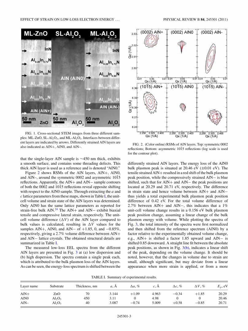
Figure 2 shows RSMs of the AlN layers, AlN+, AlN0,and AlN–, around the symmetric 0002 and asymmetric 1015reflections. Apparently, the AlN+ and AlN− sample contoursof both the 0002 and 1015 reflections reveal opposite shiftingwith respect to the AlN0 sample. Through extracting the a andc lattice parameters from these maps, shown in Table I, the unit-cell volume and strain state of the AlN layers was determined.Only AlN0 has the same lattice parameters as reported forstrain-free bulk AlN.24 The AlN+ and AlN− exhibit biaxialtensile and compressive lateral strain, respectively. The unit-cell volume difference (�V ) of the AlN layer compared tobulk values is calculated, resulting in �V values for thesamples AlN+, AlN0, and AlN− of +1.85, 0, and −0.85%,respectively, giving a 2.7% volume difference between AlN+and AlN− lattice crystals. The obtained structural details aresummarized in Table I.
The measured low-loss EEL spectra from the differentAlN layers are presented in Fig. 3 at (a) low dispersion and(b) high dispersion. The spectra contain a single peak each,which is attributed to the bulk plasmon loss of the AlN layers.As can be seen, the energy-loss spectrum is shifted between the
FIG. 2. (Color online) RSMs of AlN layers. Top: symmetric 0002reflections; Bottom: asymmetric 1015 reflections (log scale is usedfor the contour plot).
differently strained AlN layers. The energy loss of the AlN0bulk plasmon peak is situated at 20.46 eV (±0.01 eV). Thetensile strained AlN+ resulted in a red shift of the bulk plasmonpeak position, while the compressively strained AlN− is blueshifted, such that for AlN+ and AlN− the peak positions arelocated at 20.29 and 20.71 eV, respectively. The differencein strain state and hence volume between AlN+ and AlN−thus yields a total experimental bulk plasmon peak positiondifference of 0.42 eV. For the total volume difference of2.7% between AlN+ and AlN−, this indicates that a 1%unit-cell volume change results in a 0.156 eV bulk plasmonpeak position change, assuming a linear change of the bulkplasmon energy with volume. While plotting the spectra ofFig. 3, the total intensity of the spectra were first normalizedand then shifted from the reference spectrum (AlN0) by afactor relative to the experimentally obtained volume change,e.g., AlN+ is shifted a factor 1.85 upward and AlN− isshifted 0.85 downward. A straight line fit between the absolutepeak positions, as shown in Fig. 3(b), indicates a linear shiftof the peak, depending on the volume change. It should benoted, however, that the changes in volume due to strain aresmall, although significant, but may deviate from a linearappearance when more strain is applied, or from a more
TABLE I. Summary of experimental results.
Layer name Substrate Thickness, nm a, A �a, % c, A �c, % �V , % Ep , eV
AlN+ ZnO 70 3.144 +1.09 4.963 −0.34 +1.85 20.29AlN0 Al2O3 450 3.11 0 4.98 0 0 20.46AlN– Al2O3 40 3.087 −0.74 5.009 +0.58 −0.85 20.71
245301-3

J. PALISAITIS et al. PHYSICAL REVIEW B 84, 245301 (2011)
FIG. 3. (Color online) Deconvoluted low-loss EELS spectra fromthe three differently strained AlN layers at low dispersion (a) and highdispersion (b).
accurate measurement of the peak position. The results fromthe low-loss EELS measurement are summarized in Table I.
Figures 4 and 5 present the results from full potentialcalculations of the optical properties of AlN, revealing theimpact of the lattice parameters on the energy-loss function.Only the interval of the energy-loss function where the mainpeak is located is shown. Figure 4 shows the simulatedenergy-loss spectra for when the AlN unit-cell volume is keptconstant while inversely scaling a and c, i.e., by applying anisochoric strain to the unit cell, where the constant volume wascalculated from the relaxed AlN lattice parameters. The changein the c parameter is indicated in the figure, ranging from−1% to +1%. Figure 4 suggests that the appearance of theenergy-loss function is not significantly affected by this typeof lattice disturbance, although fine differences may be found.Considering that these calculations were carried out usingonly a 0.1 eV Gaussian broadening routine, these differencesare, however, challenging to detect experimentally, even ifa monochromated TEM was used. The simulated low-lossfunction of AlN, as the unit-cell volume is linearly variedfrom −3% to +3%, while simultaneously keeping the c/a
ratio constant (both a and c change by +/ −1%) is shown inFig. 5. Here the ratio was obtained from the relaxed AlN latticeparameters. This nonisochoric strain results in a continuousshift of the bulk plasmon peak as well as the interbandtransitions. Following, for reference, one of the fine peakson the central bulk plasmon peak of the function [Figs. 5(a)and 5(b)], one finds that in concert with the volume change,the peak shift is also linear, which is also seen for the spectra inFigs. 5(c) and 5(d), in which the broadened (by 1 eV) versionsof the relaxed and +/−3% volume increase-strained unit cellsare plotted.
V. DISCUSSION
The investigated AlN layers are found to be in relaxed andoppositely strained states due to different growth conditionswith substrate type and growth temperature as well as layerthickness. AlN grown on the different substrates experiences a
FIG. 4. (Color online) Simulated low-loss EELS spectra of AlNas a function of strain for constant cell volume, xx component (a)and zz component (b) and broadened spectra for xx component (c)and zz component (d).
lattice mismatch, which for AlN on ZnO and Al2O3 is −4.3%and +13.3%, respectively. As a result, residual biaxial tensileand compressive strains are present in the films that are undernon- or incomplete relaxation, as was shown by RSM. A partialstrain relaxation over thickness can be observed in the 0002reflection of the AlN0 map (see Fig. 2), where the reflectionshows asymmetric contours. The smallest transverse scatteringvector (Qz) value of the contour tail is very close to that of thethin AlN layer in the AlN− contour. This tail is attributed tothe evolution of strain relaxation from the interface toward thefilm surface. Details about strain formation in the Al1-xInxNlayers can be found elsewhere.19
The low-loss spectra in Fig. 3 contain only one strong signalthat is attributed to the bulk plasmon, which is a collectiveoscillation of the valence electrons. In the free electron theory,the valence electrons give a bulk plasmon energy according to
Ep = hωp = h
(ne2
ε0m0
)1/2
, (1)
where n is the density of electrons, e is the electron charge, ε0
is the permittivity of free space, and m0 is the electron mass.
245301-4

EFFECT OF STRAIN ON LOW-LOSS ELECTRON ENERGY . . . PHYSICAL REVIEW B 84, 245301 (2011)
FIG. 5. (Color online) Simulated low-loss EELS spectrum of AlNby changing unit-cell volume (–3% to +3%) and keeping the c/a ratioconstant, xx component (a) and zz component (b) and broadenedspectra for xx component (c) and zz component (d).
This model gives a good approximation to the measured bulkplasmon energy, particularly for metallic systems.15 However,it does not take into account damping of the bulk plasmon,which broadens the peak, and intraband transitions, whichadds fine structure to the low-loss spectrum.
To resolve this shortcoming, we consider the fast electronpassing through the sample as a time-varying electric field.The induced electric field in the material as a response tothe electron is then given by the dielectric function in thesmall-angle region ε(E) = ε1(E) + iε2(E). Furthermore, thesingle scattering distribution may be written in the form15,18,23
S(E) = 2I0t
πa0m0ν2Im
( −1
ε(E)
)ln
[1 +
(β
θE
)2], (2)
where I0 is the incident intensity, t the specimen thickness,ν the speed of the incident electrons, β is the collectionsemiangle, and θE =E/(γm0ν
2) is the characteristic scatteringangle (where γ = 1 − ν2/c2), and ignoring the need forcorrection factors due to the high convergence/collection
angle ratio. Thus the scattering distribution is proportionalto Im[–1/ε(E)], where
Im
( −1
ε(E)
)= ε2(E)
ε21(E) + ε2
2(E)(3)
is known as the loss function. In principle, at large energylosses, ε1(E) approaches 1 while ε2(E) is small,12 such thatthe energy-loss function is reduced to S(E) ≈ ε2(E), althoughin most cases ε1(E) cannot be ignored. However, it is desirableto calculate ε2(E), since from this point it is possible to useKramers-Kronig analysis to retrieve ε1(E). In the WIEN2K
calculations applied here, ε2(E) is obtained from the randomphase approximation (RPA),20 which employs wave functionsof the core and valence states, which are initially calculatedby WIEN2K. Employing WIEN2K, it may be found that the realpart ε1(E) of the dielectric function gives the bulk plasmonwhile the imaginary part ε2(E) gives the intraband transitionsof the energy loss function as it was calculated in this paper. Bycomparing with the calculated real and imaginary parts of thedielectric function (not shown), the strong and slowly varyingpeaks throughout these calculations are attributed to bulkplasmons, while the finer structure is attributed to intrabandtransitions.
In these simulations a seemingly linear variation of theplasmon peak position is identified when the crystal volume ischanged (Fig. 5). However, the peak position is not changedwhile changing the c/a ratio and keeping the volume constant(Fig. 4). The electron density is changed while calculatingthe loss functions for the different crystal volumes in Fig. 5.For a quick indication, Eq. (1) shows that the plasmon energyis proportional to electron density
12 , indicating a nonlinear
relation between the two. However, for such small changesas are observed here, the nonlinear behavior may appear as aseemingly linear variation.
To test the reliability of these calculations, the experi-mentally obtained lattice parameters for AlN+, AlN0, andAlN− were used as input. The resulting calculated energy-lossfunctions are shown in Fig. 6 for Gaussian broadenings of 0.1and 1 eV. As with the experimental spectra, the intensity is
FIG. 6. (Color online) Simulated low-loss EELS spectrum ofAlN by using experimentally determined lattice parameters, xx
component (a) and zz component (b).
245301-5

J. PALISAITIS et al. PHYSICAL REVIEW B 84, 245301 (2011)
TABLE II. Comparison of simulated (using experimental latticeconstants) and experimental plasmon peak position values fordifferently strained AlN layers.
Calculated Rel. Cal. Expt. AlN Rel. Expt.Layer name AlN (xx), eV AlN (xx), eV Ep , eV AlN, eV
AlN+ 21.13 −0.24 20.29 −0.17AlN0 21.37 0 20.46 0AlN– 21.56 +0.19 20.71 +0.25
normalized and shifted from the unstrained sample by a factorcorresponding to the volume change. Also, here it is foundthat the plasmon is shifted linearly depending on volume,although the c/a ratio is not the same for either the AlN+,AlN0, or AlN–, which was the case in Fig. 5. This suggeststhat the plasmon peak position shift is more depending onthe associated volume change than differences in a or c
individually. This also indicates that the strain in both a andc cannot be obtained separately from a measurement of thebulk plasmon peak energy alone. Although the simulated peakpositions do not perfectly fit the experimental ones (they areshifted by 1.1 eV), their relative peak shift matches. The AlN+peak is found with a maximum at 21.11 eV, the unstrainedAlN0 at 21.37 eV, and finally for the AlN–, the peak energywas 21.56 eV. The total energy difference between AlN+ andAlN− was 0.44 eV. This gives a calculated shift of 0.159 eVper 1% volume change as compared to the experimentallymeasured shift of 0.156 eV. A comparison of simulated (usingexperimental lattice constants) and experimental bulk plasmonpeak position values for the differently strained AlN layers isgiven in Table II.
Similar calculations were applied to GaN and InN, wherethe plasmon peak energy is located at 19.4 eV for GaN28
and 14.95 eV for InN as determined experimentally,16 and theresults are shown for the relaxed and +/−3% volume unitcells in Fig. 7. Here, the energy-loss function is more complexwith significantly stronger intraband contributions. However,by following the bulk plasmon shift for the broadened spectrumfor each structure, as is indicted in Fig. 7, the relativeenergy shifts per 1% volume change are 0.168 eV for GaNand 0.079 eV for InN. These numbers are of a similarorder as for AlN. The simulation results are summarized inTable III.
By alloying these nitrides, we recently found that theplasmon peak changes linearly in the interval between thepure components.16 We suggest here that a ternary nitridealloy, which is subject to strain, experiences a similar shift ofthe plasmon peak position away from the relaxed value, as forthe binary nitrides discussed above.
Without prior knowledge of the exact composition of analloy, it is possible to determine this by determining thebulk plasmon peak position. However, employing this methodassumes a relaxed structure, so the composition of a crystalmight be over- or underestimated because of the strain-inducedshifts the bulk plasmon energy. For Al1-xInxN alloys, wherethe plasmon ranges from 14.95 to 20.4 eV,16 the compositionalerror is only ∼3% for a 1% increase in volume in Al-richAl1-xInxN and ∼9% for a 1% increase in both a and c lattice
FIG. 7. (Color online) Simulated low-loss EELS spectrum of InNand GaN by changing the unit-cell volume from −3% to +3% andkeeping the c/a ratio constant for the components (a) GaN xx,(b) GaN zz, (c) InN xx, and (d) zz.
parameters (3% change in volume). On the other hand, forAl1-xGaxN where the plasmon energy range is only 1 eV, thecompositional error is ∼16% for a 1% change in volume andan alarming ∼48% for a 1% increase in both a and c latticeparameters (3% change in volume).
Applying spectrum imaging methods to nanoscale struc-tures such as quantum wells and ignoring for the purposeof this discussion the delocalization effect of the low-lossfeatures,29 the map or line scan along the nanostructure willshow a variation in the plasmon energy across the interface dueto variations in composition. Since the two materials on eitherside of the interface are usually not perfectly lattice matched,at least the quantum material will experience strain, affectingplasmon peak position as well. The plasmon energy of thequantum structure cannot directly reveal the composition.However, if a and c are known from, e.g., a lattice image,the crystal volume is known. Then the bulk plasmon positioncan be used to determine the composition and the strain of thelattice.
245301-6

EFFECT OF STRAIN ON LOW-LOSS ELECTRON ENERGY . . . PHYSICAL REVIEW B 84, 245301 (2011)
TABLE III. Calculated bulk plasmon peak position values for InN, GaN, and AlN (xx and zz components).
�V , % InN (xx), eV InN (zz), eV GaN (xx), eV GaN (zz), eV AlN (xx), eV AlN (zz), eV
+3% 15.19 15.02 20.17 20.79 20.81 21.290 15.43 15.29 20.68 21.32 21.37 21.73−3% 15.66 15.55 21.18 21.84 21.78 22.14
VI. CONCLUSIONS
The low-loss EELS spectrum is affected by the strain statein group-III nitrides, which was shown by a combination ofexperimental and theoretical experiments. It is found that thebulk plasmon peak position varies nearly linearly with theunit-cell volume, at least up to a 3% volume change Thiscan be used to retrieve information about the strain in thematerial. Specifically, a volume change of 1% results in a peakshift of 0.159, 0.168, and 0.079 eV for AlN, GaN, and InN,respectively. The AlN peak shift was confirmed experimentallywith a measured peak shift of 0.156 eV per 1% volume change.This result has particular relevance for low-loss mappingstudies of confined and nanoscale structures in alloys ofgroup-III nitrides. As strain and compositional gradients aretypically present across the interfaces of these, it is difficult todiscern which of these causes a shift in the low-loss spectrum.It is further concluded that strain has a lower impact onthe peak shift in Al1-xInxN and In1-xGaxN alloys than for
Al1-xGaxN. For example, a 1% volume change in Al1-xInxNcauses a detectable peak shift, which could be misinterpretedfor a 3% compositional variation of Al and In. With a similarpeak shift, for Al1-xGaxN, the 1% volume change may bemisinterpreted for an ∼16% composition change. As strainbetween layers of widely differing composition that are afew monolayers thick can be larger than this, low-loss studiesmust be undertaken with a full knowledge of both the strainstate and the composition of the material. Identification of thetwo components can be obtained by real or reciprocal spacemeasurements for the lattice spacing combined with low-lossEELS.
ACKNOWLEDGMENTS
This work was supported by the Swedish Research Council(VR), the Swedish Foundation for Strategic Research (SSF),and The Royal Swedish Academy of Sciences (KVA).
*[email protected]. Wu, J. Appl. Phys. 106, 011101 (2009).2M. Razeghi and R. McClintock, J. Cryst. Growth 311, 3067 (2009).3M. Chu, Y. Sun, U. Aghoram, and S. E. Thompson, Annu. Rev.Mater. Res. 39, 203 (2009).
4W. Zhao, G. Duscher, G. Rozgonyi, M. A. Zikry, S. Chopra, andM. C. Ozturk, Appl. Phys. Lett. 90, 191907 (2007).
5V. Darakchieva, M. Beckers, M. Xie, L. Hultman, B. Monemar,J. Carlin, E. Feltin, M. Gonschorek, and N. Grandjean, J. Appl.Phys. 103, 103513 (2008).
6J. Chung, G. Lian, and L. Rabenberg, Appl. Phys. Lett. 93, 081909(2008).
7P. L. Galindo, S. Kret, A. M. Sanchez, J. Laval, A. Yanez, J. Pizarro,E. Guerrero, T. Ben, and S. I. Molina, Ultramicroscopy 107, 1186(2007).
8P. Zhang, A. A. Istratov, E. R. Weber, C. Kisielowski, H. He,C. Nelson, and J. C. H. Spence, Appl. Phys. Lett. 89, 161907 (2006).
9A. Beche, J. L. Rouviere, L. Clement, and J. M. Hartmann, Appl.Phys. Lett. 95, 123114 (2009).
10M. Hytch, F. Houdellier, F. Hue, and E. Snoeck, Nature 453, 1086(2008).
11F. Houdellier, M. J. Hytch, E. Snoeck, and M. J. Casanove, Mater.Sci. Eng. B 135, 188 (2006).
12R. F. Egerton, Electron Energy loss Spectroscopy in the ElectronMicroscope (Plenum, New York, 1996).
13H. Raether, Excitations of Plasmons and Interband Transitions byElectrons (Springer, Berlin, 1980).
14V. J. Keast, J. Electron Spectrosc. 143, 97 (2005).15A. M. Sanchez, R. Beanland, M. H. Gass, A. J. Papworth, P. J.
Goodhew, and M. Hopkinson, Phys. Rev. B 72, 075339 (2005).
16J. Palisaitis, C.-L. Hsiao, M. Junaid, M. Xie, V. Darakchieva,J. Carlin, N. Grandjean, J. Birch, L. Hultman, and P. O. A. Persson,Phys. Status Solidi (RRL) 5, 50 (2011).
17N. D. Browning, I. Arslan, R. Erni, J. C. Idrobo, A. Ziegler,J. Bradley, Z. Dai, E. A. Stach, and A. Bleloch, J. Phys. Conf.Ser. 26, 59 (2006).
18A. Gubbens, M. Barfels, C. Trevor, R. Twesten, P. Mooney,P. Thomas, N. Menon, B. Kraus, C. Mao, and B. McGinn,Ultramicroscopy 110, 962 (2010).
19C.-L. Hsiao, J. Palisaitis, M. Junaid, P. O. A. Persson, J. Jensen, andJ. Birch, Thin Solid Films (submitted).
20R. F. Egerton, Micron 34, 127 (2003).21A. Maigne and R. D. Twesten, J. Electron Microsc. 58, 99 (2009);
[http://www.rzg.mpg.de/∼mam].22K. Schwarz and P. Blaha, Comput. Mater. Sci. 28, 259
(2003).23H. Morkoc, Nitride Semiconductors and Devices (Springer-Verlag,
Germany, 1999).24T. Yao and S. K. Hong, Oxide and Nitride Semiconductors: Pro-
cessing, Properties, and Applications (Springer-Verlag, Germany,2009).
25C. Ambrosch-Draxl and J. O. Sofo, Comput. Phys. Commun. 175,1 (2006).
26C. Ambrosch-Draxl, J. A. Majewski, P. Vogl, and G. Leising, Phys.Rev. B 51, 9668 (1995).
27P. Schattschneider, Ultramicroscopy 28, 1 (1989).28V. J. Keast, A. J. Scott, M. J. Kappers, C. T. Foxon, and C. J.
Humphreys, Phys. Rev. B 66, 125319 (2002).29D. A. Muller and J. Silcox, Ultramicroscopy 59, 195
(1995).
245301-7