Effect of Mechanical Milling Time on Helium Irradiation ...
7
Rare Metal Materials and Engineering Volume 48, Issue 8, August 2019 Available online at www.rmme.ac.cn Cite this article as: Rare Metal Materials and Engineering, 2019, 48(8): 2406-2412. Received date: August 24, 2018 Foundation item: National Magnetic Confinement Fusion Program (2014GB121001); National Natural Science Foundation of China (51474083); The Foundation of Laboratory of Nonferrous Metal Material Processing Engineering of Anhui Province (15CZS08031); “111” Project of China (B18018) Corresponding author: Luo Laima, Ph. D., Professor, School of Materials Science and Engineering, Hefei University of Technology, Hefei 230009, P. R. China, Tel: 0086-551-62902604, E-mail: [email protected] Copyright © 2019, Northwest Institute for Nonferrous Metal Research. Published by Science Press. All rights reserved. ARTICLE Science Press Effect of Mechanical Milling Time on Helium Irradiation Behavior of W-Nb Alloys Luo Laima 1,3 , Xu Mengyao 1 , Zan Xiang 1,3 , Xu Qiu 4 , Zhu Xiaoyong 1,3 , Liu Jia- qin 2 , Cheng Jigui 1,3 , Wu Yucheng 1,3,5 1 School of Materials Science and Engineering, Hefei University of Technology, Hefei 230009, China; 2 Industry & Equipment Technology, Hefei University of Technology, Hefei 230009, China; 3 Laboratory of Nonferrous Metal Material and Processing Engineering of Anhui Province, Hefei 230009, China; 4 Kyoto University, Osaka-fu 590-0494, Japan; 5 National-Local Joint Engineering Research Centre of Nonferrous Metals and Processing Technology, Hefei 230009, China Abstract: Mechanical milling can easily obtain nanopowders and consolidate milled powders to full density. Milling time exerts a critical influence on the performance of powders and bulk materials. In this study, the tungsten (W) combined with niobium (Nb) powder was wet milled for 15, 25, 36, and 45 h, and consolidated by spark plasma sintering. The W-Nb specimens were irradiated by 9.90×10 24 ions m -2 helium (He) beams for 11 min. The results show that solid solution degree of W and Nb influences the irradiation damage of the specimen. The specimen milled for 36 h has the lowest solid solution degree, whose surface damage is the most serious among all specimens, and the nanostructure “fuzz” forms only in this specimen. In the same specimen, tungsten presents different surface damage degrees owing to its different orientations. After characterization, the W-Nb specimens were isochronally annealed at 900, 1100, and 1300 °C for 1 h. The grains grow in Nb-rich area but barely change in W-rich area, because Nb exerts a strong influence on the right shifting of He desorption peaks. Key words: W-Nb alloys; mechanical milling; spark plasma sintering; helium irradiation; annealing Tungsten (W) is a promising controllable plasma-facing material in nuclear fusion devices because of its superb properties, such as high melting point, sputtering threshold, and low tritium retention. When W is bombarded by high fluxes of low-energy helium (He) particles and neutrons at high temperatures, its surfaces form a nanostructure called “W fuzz” at temperatures between 1000 and 2000 K, landing energies above 20 eV, and fluxes obviously higher than 2×10 20 m -2 ·s -1 [1,2] . These nanotendrils have been produced in linear plasma devices [3-5] and Alcator C-Mod [3,6] . The effect of fuzz on plasma-surface interaction mechanism and tokamak operations is still uncertain. However, the fuzz layers present low sputtering yield in bulk W [7] and are sensitive to uni-polar arcing [8] . W performance is restricted by inappropriate ductile-to- brittle transition temperatures. The ductility of W should be ameliorated to avoid thermal stress in fusion devices, which can be achieved by combining other ductile refractory metals [9] . Niobium (Nb) presents outstanding ductility in group V-B [10] . Niobium has a high melting point, corrosion resistance, and low thermal-neutron absorption cross-section. On the other hand, niobium has a high affinity for impurities such as O, C, and N, and can be bound with these impurity elements to form compounds with high melting temperatures, which can decrease the total retention D 2 and clean the grain boundary of W alloys. A small amount of niobium can improve the ductility of tungsten-based materials and alter their behaviors under irradiation. Unlike wet chemical methods, mechanical milling can easily obtain nanopowders and consolidate the milled powders
Transcript of Effect of Mechanical Milling Time on Helium Irradiation ...
Rare Metal Materials and Engineering
Volume 48, Issue 8, August 2019
Available online at www.rmme.ac.cn
Cite this article as: Rare Metal Materials and Engineering, 2019, 48(8): 2406-2412.
Received date: August 24, 2018
Foundation item: National Magnetic Confinement Fusion Program (2014GB121001); National Natural Science Foundation of China (51474083); The Foundation of
Laboratory of Nonferrous Metal Material Processing Engineering of Anhui Province (15CZS08031); “111” Project of China (B18018)
Corresponding author: Luo Laima, Ph. D., Professor, School of Materials Science and Engineering, Hefei University of Technology, Hefei 230009, P. R. China, Tel:
0086-551-62902604, E-mail: [email protected]
Copyright © 2019, Northwest Institute for Nonferrous Metal Research. Published by Science Press. All rights reserved.
ARTICLE
Science Press
Effect of Mechanical Milling Time on Helium Irradiation
Behavior of W-Nb Alloys
Luo Laima
1,3
, Xu Mengyao
1
, Zan Xiang
1,3
, Xu Qiu
4
, Zhu Xiaoyong
1,3
, Liu Jia-
qin
2
, Cheng Jigui
1,3
, Wu Yucheng
1,3,5
1
School of Materials Science and Engineering, Hefei University of Technology, Hefei 230009, China;
2
Industry & Equipment Technology,
Hefei University of Technology, Hefei 230009, China;
3
Laboratory of Nonferrous Metal Material and Processing Engineering of Anhui
Province, Hefei 230009, China;
4
Kyoto University, Osaka-fu 590-0494, Japan;
5
National-Local Joint Engineering Research Centre of
Nonferrous Metals and Processing Technology, Hefei 230009, China
Abstract: Mechanical milling can easily obtain nanopowders and consolidate milled powders to full density. Milling time exerts a
critical influence on the performance of powders and bulk materials. In this study, the tungsten (W) combined with niobium (Nb)
powder was wet milled for 15, 25, 36, and 45 h, and consolidated by spark plasma sintering. The W-Nb specimens were irradiated
by 9.90×10
24
ions m
-2
helium (He) beams for 11 min. The results show that solid solution degree of W and Nb influences the
irradiation damage of the specimen. The specimen milled for 36 h has the lowest solid solution degree, whose surface damage is the
most serious among all specimens, and the nanostructure “fuzz” forms only in this specimen. In the same specimen, tungsten
presents different surface damage degrees owing to its different orientations. After characterization, the W-Nb specimens were
isochronally annealed at 900, 1100, and 1300 °C for 1 h. The grains grow in Nb-rich area but barely change in W-rich area, because
Nb exerts a strong influence on the right shifting of He desorption peaks.
Key words: W-Nb alloys; mechanical milling; spark plasma sintering; helium irradiation; annealing
Tungsten (W) is a promising controllable plasma-facing
material in nuclear fusion devices because of its superb
properties, such as high melting point, sputtering threshold,
and low tritium retention.
When W is bombarded by high fluxes of low-energy helium
(He) particles and neutrons at high temperatures, its surfaces
form a nanostructure called “W fuzz” at temperatures between
1000 and 2000 K, landing energies above 20 eV, and fluxes
obviously higher than 2×10
20
m
-2
·s
-1
[1,2]
. These nanotendrils
have been produced in linear plasma devices
[3-5]
and Alcator
C-Mod
[3,6]
. The effect of fuzz on plasma-surface interaction
mechanism and tokamak operations is still uncertain. However,
the fuzz layers present low sputtering yield in bulk W
[7]
and
are sensitive to uni-polar arcing
[8]
.
W performance is restricted by inappropriate ductile-to-
brittle transition temperatures. The ductility of W should be
ameliorated to avoid thermal stress in fusion devices, which
can be achieved by combining other ductile refractory
metals
[9]
. Niobium (Nb) presents outstanding ductility in
group V-B
[10]
. Niobium has a high melting point, corrosion
resistance, and low thermal-neutron absorption cross-section.
On the other hand, niobium has a high affinity for impurities
such as O, C, and N, and can be bound with these impurity
elements to form compounds with high melting temperatures,
which can decrease the total retention D
2
and clean the grain
boundary of W alloys. A small amount of niobium can
improve the ductility of tungsten-based materials and alter
their behaviors under irradiation.
Unlike wet chemical methods, mechanical milling can
easily obtain nanopowders and consolidate the milled powders
Luo Laima et al. / Rare Metal Materials and Engineering, 2019, 48(8): 2406-2412 2407
to full density
[11]
. Milling time exerts a critical influence on
the performance of powders and bulk materials.
In addition, this paper tries to address questions that appear
when tungsten is irradiated in high temperature environments
found in fusion reactors. In order to understand the recovery
behavior of displacement damage, quasi-in-situ annealing
experiments were performed on tungsten-niobium samples
followed by 50 eV He ion irradiation and subsequent
hydrogen atmosphere annealing. The annealing temperatures
ranged from 900 °C to 1300 °C. The annealing of bcc metals
classified by Thompson
[12]
involves five stages. Stage I occurs
below −170 °C due to the movement of free interstitials
[13]
.
Stage II occurs at −170~350 °C, ascribed to the release of
interstitials from trap with activation energies of 0.25~1.7 eV.
The fusion reactor operates at 500~1000 °C
[14]
. The study of
stages III~V is meaningful for first-wall materials. Stage III,
with the temperature of ~350 °C/~0.15 T
m
and activation
energy of ~1.7 eV, is due to the monovacancy mobility
activation
[13]
. Stage IV at 640 °C/0.22 T
m
is ascribed to
vacancy-impurity complex
[14]
, or di-vacancy
[15]
. Stage V or
the recovery stage at 0.31 T
m
is due to vacancy migration
[16]
but that at high temperatures is attributed to the disappearance
of defect cluster or formation of voids
[17]
. This experiment
mainly occurs in stage V.
This experimental study aims to investigate the behavior of
He-induced nanostructures in W-Nb alloys with different
milling time.
1 Experiment
The powders used in this study contained 85 wt% pure W
(>99.9%, 1.0~1.3 µm) and 15 wt% pure Nb (>99.9%, 40~50
µm), and were prepared by ball milling. Mechanical milling
was performed in a planetary ball mill with a rotation speed of
400 r/min and a ball to powder ratio of 20:1 at room
temperature, whose jar and ball were made of tungsten carbide
(WC). The milling medium was absolute ethyl alcohol, and
the milling time was 15, 25, 36, and 45 h. The powder was
soaked in alcohol with air included in the pot. The powder was
loaded in a graphite die with a diameter of approximately 20
mm. Then, DC current was applied to the pulse, and the high
uniaxial mechanical pressure was obtained in this process. The
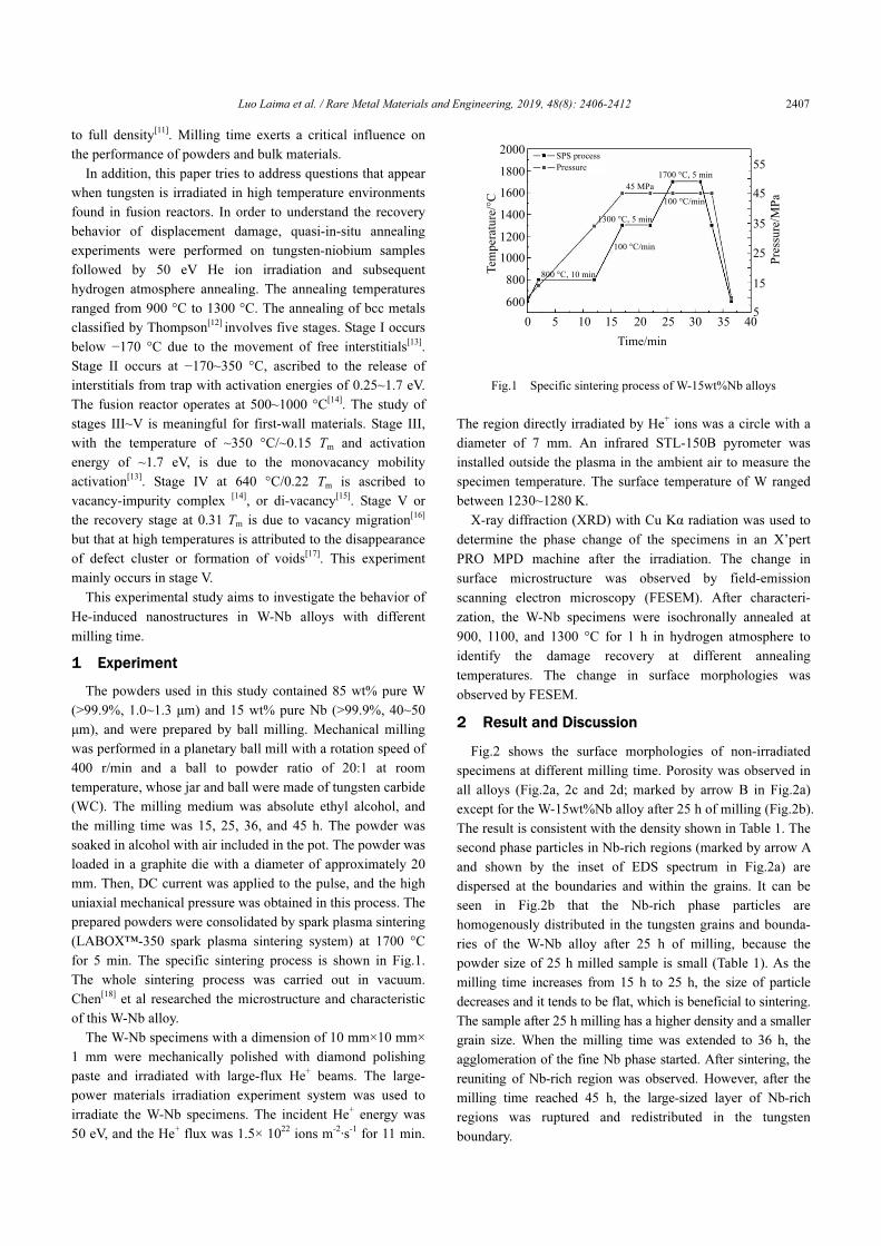
prepared powders were consolidated by spark plasma sintering
(LABOX™-350 spark plasma sintering system) at 1700 °C
for 5 min. The specific sintering process is shown in Fig.1.
The whole sintering process was carried out in vacuum.
Chen
[18]
et al researched the microstructure and characteristic
of this W-Nb alloy.
The W-Nb specimens with a dimension of 10 mm×10 mm×
1 mm were mechanically polished with diamond polishing
paste and irradiated with large-flux He
+
beams. The large-
power materials irradiation experiment system was used to
irradiate the W-Nb specimens. The incident He
+
energy was
50 eV, and the He
+
flux was 1.5× 10
22
ions m
-2
·s
-1
for 11 min.
Fig.1 Specific sintering process of W-15wt%Nb alloys
The region directly irradiated by He
+
ions was a circle with a
diameter of 7 mm. An infrared STL-150B pyrometer was
installed outside the plasma in the ambient air to measure the
specimen temperature. The surface temperature of W ranged
between 1230~1280 K.
X-ray diffraction (XRD) with Cu Kα radiation was used to
determine the phase change of the specimens in an X’pert
PRO MPD machine after the irradiation. The change in
surface microstructure was observed by field-emission
scanning electron microscopy (FESEM). After characteri-
zation, the W-Nb specimens were isochronally annealed at
900, 1100, and 1300 °C for 1 h in hydrogen atmosphere to
identify the damage recovery at different annealing
temperatures. The change in surface morphologies was
observed by FESEM.
2 Result and Discussion
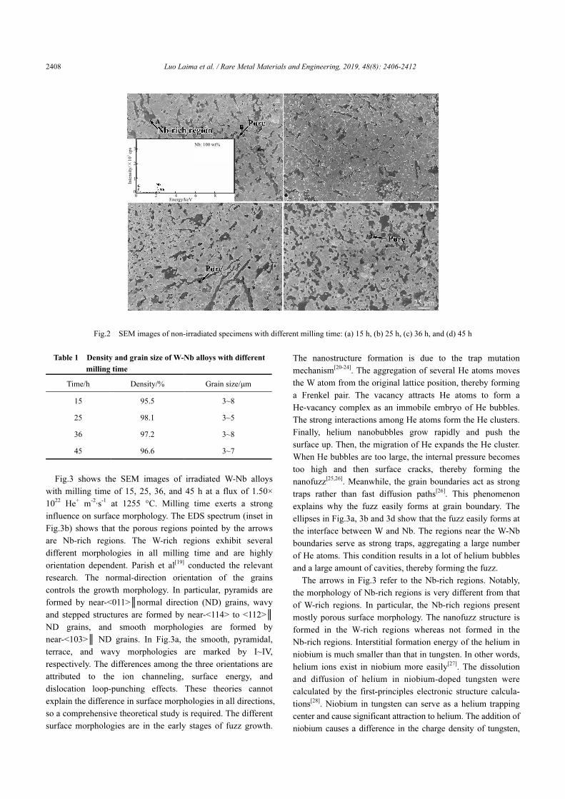
Fig.2 shows the surface morphologies of non-irradiated
specimens at different milling time. Porosity was observed in
all alloys (Fig.2a, 2c and 2d; marked by arrow B in Fig.2a)
except for the W-15wt%Nb alloy after 25 h of milling (Fig.2b).
The result is consistent with the density shown in Table 1. The
second phase particles in Nb-rich regions (marked by arrow A
and shown by the inset of EDS spectrum in Fig.2a) are
dispersed at the boundaries and within the grains. It can be
seen in Fig.2b that the Nb-rich phase particles are
homogenously distributed in the tungsten grains and bounda-
ries of the W-Nb alloy after 25 h of milling, because the
powder size of 25 h milled sample is small (Table 1). As the
milling time increases from 15 h to 25 h, the size of particle
decreases and it tends to be flat, which is beneficial to sintering.
The sample after 25 h milling has a higher density and a smaller
grain size. When the milling time was extended to 36 h, the
agglomeration of the fine Nb phase started. After sintering, the
reuniting of Nb-rich region was observed. However, after the
milling time reached 45 h, the large-sized layer of Nb-rich
regions was ruptured and redistributed in the tungsten
boundary.
0 5 10 15 20 25 30 35 40
Time/min
2000
1800
1600
1400
1200
1000
800
600
Tem
peratu
re/°C
55
45
35
25
15
5
Pressu
re/M
Pa
1700 °C, 5 min
100 °C/min
1300 °C, 5 min
45 MPa
100 °C/min
800 °C, 10 min
SPS process
Pressure
2408 Luo Laima et al. / Rare Metal Materials and Engineering, 2019, 48(8): 2406-2412
Fig.2 SEM images of non-irradiated specimens with different milling time: (a) 15 h, (b) 25 h, (c) 36 h, and (d) 45 h
Table 1 Density and grain size of W-Nb alloys with different
milling time
Time/h Density/% Grain size/µm
15 95.5 3~8
25 98.1 3~5
36 97.2 3~8
45 96.6 3~7
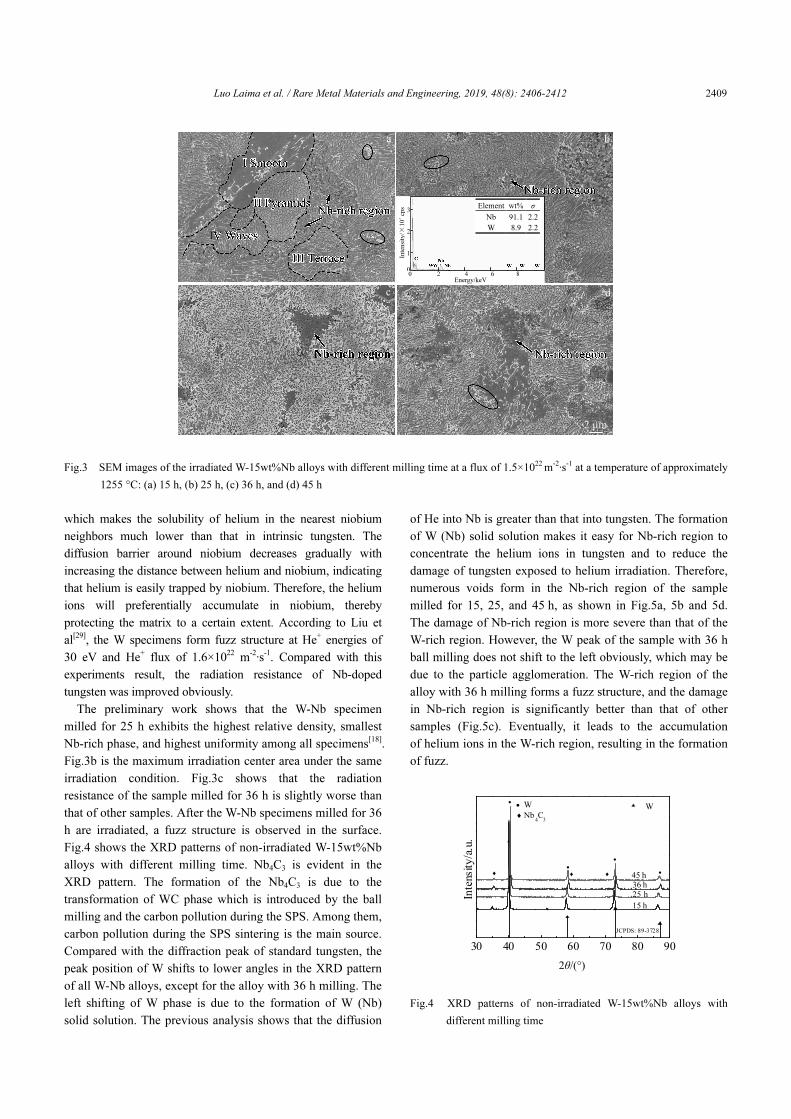
Fig.3 shows the SEM images of irradiated W-Nb alloys
with milling time of 15, 25, 36, and 45 h at a flux of 1.50×
10
22
He
+
m
-2
·s
-1
at 1255 °C. Milling time exerts a strong
influence on surface morphology. The EDS spectrum (inset in
Fig.3b) shows that the porous regions pointed by the arrows
are Nb-rich regions. The W-rich regions exhibit several
different morphologies in all milling time and are highly
orientation dependent. Parish et al
[19]
conducted the relevant
research. The normal-direction orientation of the grains
controls the growth morphology. In particular, pyramids are
formed by near-<011>║normal direction (ND) grains, wavy
and stepped structures are formed by near-<114> to <112>║
ND grains, and smooth morphologies are formed by
near-<103>║ ND grains. In Fig.3a, the smooth, pyramidal,
terrace, and wavy morphologies are marked by I~IV,
respectively. The differences among the three orientations are
attributed to the ion channeling, surface energy, and
dislocation loop-punching effects. These theories cannot
explain the difference in surface morphologies in all directions,
so a comprehensive theoretical study is required. The different
surface morphologies are in the early stages of fuzz growth.
The nanostructure formation is due to the trap mutation
mechanism
[20-24]
. The aggregation of several He atoms moves
the W atom from the original lattice position, thereby forming
a Frenkel pair. The vacancy attracts He atoms to form a
He-vacancy complex as an immobile embryo of He bubbles.
The strong interactions among He atoms form the He clusters.
Finally, helium nanobubbles grow rapidly and push the
surface up. Then, the migration of He expands the He cluster.
When He bubbles are too large, the internal pressure becomes
too high and then surface cracks, thereby forming the
nanofuzz
[25,26]
. Meanwhile, the grain boundaries act as strong
traps rather than fast diffusion paths
[26]
. This phenomenon
explains why the fuzz easily forms at grain boundary. The
ellipses in Fig.3a, 3b and 3d show that the fuzz easily forms at
the interface between W and Nb. The regions near the W-Nb
boundaries serve as strong traps, aggregating a large number
of He atoms. This condition results in a lot of helium bubbles
and a large amount of cavities, thereby forming the fuzz.
The arrows in Fig.3 refer to the Nb-rich regions. Notably,
the morphology of Nb-rich regions is very different from that
of W-rich regions. In particular, the Nb-rich regions present
mostly porous surface morphology. The nanofuzz structure is
formed in the W-rich regions whereas not formed in the
Nb-rich regions. Interstitial formation energy of the helium in
niobium is much smaller than that in tungsten. In other words,
helium ions exist in niobium more easily
[27]
. The dissolution
and diffusion of helium in niobium-doped tungsten were
calculated by the first-principles electronic structure calcula-
tions
[28]
. Niobium in tungsten can serve as a helium trapping
center and cause significant attraction to helium. The addition of
niobium causes a difference in the charge density of tungsten,
a
b
c
d
25 µm
3
2
1
0
0 2 4 6 8
Energy/keV
Nb: 100 wt%
In
ten
sity
/�
10
3
cp
s
Luo Laima et al. / Rare Metal Materials and Engineering, 2019, 48(8): 2406-2412 2409
Fig.3 SEM images of the irradiated W-15wt%Nb alloys with different milling time at a flux of 1.5×10
22
m
-2
·s
-1
at a temperature of approximately
1255 °C: (a) 15 h, (b) 25 h, (c) 36 h, and (d) 45 h
which makes the solubility of helium in the nearest niobium
neighbors much lower than that in intrinsic tungsten. The
diffusion barrier around niobium decreases gradually with
increasing the distance between helium and niobium, indicating
that helium is easily trapped by niobium. Therefore, the helium
ions will preferentially accumulate in niobium, thereby
protecting the matrix to a certain extent. According to Liu et
al
[29]
, the W specimens form fuzz structure at He
+
energies of
30 eV and He
+
flux of 1.6×10
22
m
-2
·s
-1
. Compared with this
experiments result, the radiation resistance of Nb-doped
tungsten was improved obviously.
The preliminary work shows that the W-Nb specimen
milled for 25 h exhibits the highest relative density, smallest
Nb-rich phase, and highest uniformity among all specimens
[18]
.
Fig.3b is the maximum irradiation center area under the same
irradiation condition. Fig.3c shows that the radiation
resistance of the sample milled for 36 h is slightly worse than
that of other samples. After the W-Nb specimens milled for 36
h are irradiated, a fuzz structure is observed in the surface.
Fig.4 shows the XRD patterns of non-irradiated W-15wt%Nb
alloys with different milling time. Nb
4
C
3
is evident in the
XRD pattern. The formation of the Nb
4
C
3
is due to the
transformation of WC phase which is introduced by the ball
milling and the carbon pollution during the SPS. Among them,
carbon pollution during the SPS sintering is the main source.
Compared with the diffraction peak of standard tungsten, the
peak position of W shifts to lower angles in the XRD pattern
of all W-Nb alloys, except for the alloy with 36 h milling. The
left shifting of W phase is due to the formation of W (Nb)
solid solution. The previous analysis shows that the diffusion
of He into Nb is greater than that into tungsten. The formation
of W (Nb) solid solution makes it easy for Nb-rich region to
concentrate the helium ions in tungsten and to reduce the
damage of tungsten exposed to helium irradiation. Therefore,
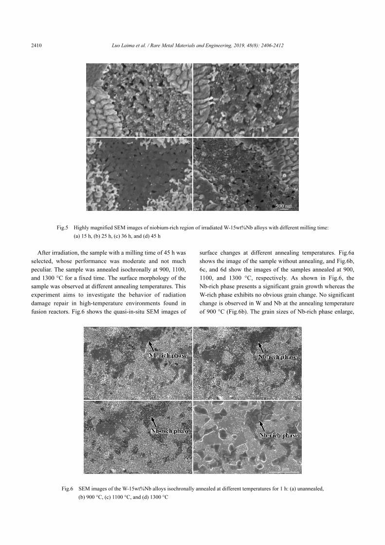
numerous voids form in the Nb-rich region of the sample
milled for 15, 25, and 45 h, as shown in Fig.5a, 5b and 5d.
The damage of Nb-rich region is more severe than that of the
W-rich region. However, the W peak of the sample with 36 h
ball milling does not shift to the left obviously, which may be
due to the particle agglomeration. The W-rich region of the
alloy with 36 h milling forms a fuzz structure, and the damage
in Nb-rich region is significantly better than that of other
samples (Fig.5c). Eventually, it leads to the accumulation
of helium ions in the W-rich region, resulting in the formation
of fuzz.
Fig.4 XRD patterns of non-irradiated W-15wt%Nb alloys with
different milling time
30 40 50 60 70 80 90
45 h
36 h
25 h
15 h
♦♦
•
•
•
W
Intensity/a.u.
♦
•
• W
♦ Nb
4
C
3
JCPDS: 89-3728
2θ/(°)
0 2 4 6 8
Energy/keV
3
2
1
0
In
ten
sity
/�
10
3
cp
s
Element wt% σ
Nb 91.1 2.2
W 8.9 2.2
a
b
d
c
2 µm
2410 Luo Laima et al. / Rare Metal Materials and Engineering, 2019, 48(8): 2406-2412
Fig.5 Highly magnified SEM images of niobium-rich region of irradiated W-15wt%Nb alloys with different milling time:
(a) 15 h, (b) 25 h, (c) 36 h, and (d) 45 h
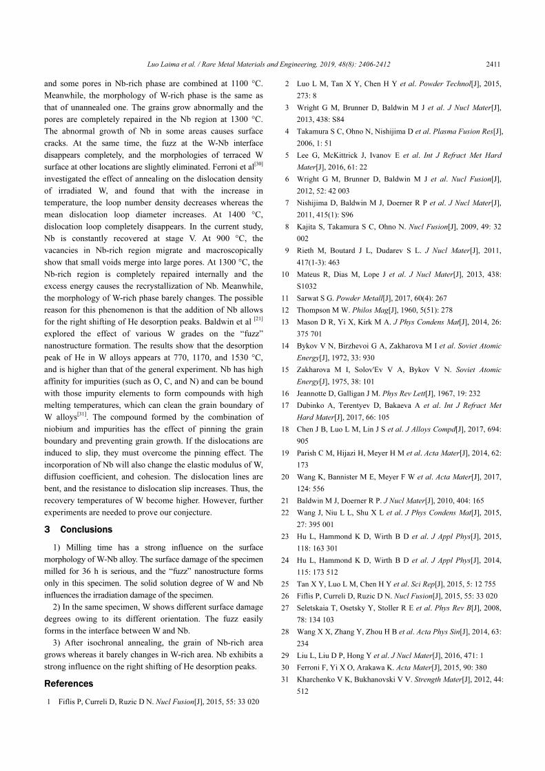
After irradiation, the sample with a milling time of 45 h was
selected, whose performance was moderate and not much
peculiar. The sample was annealed isochronally at 900, 1100,
and 1300 °C for a fixed time. The surface morphology of the
sample was observed at different annealing temperatures. This
experiment aims to investigate the behavior of radiation
damage repair in high-temperature environments found in
fusion reactors. Fig.6 shows the quasi-in-situ SEM images of
surface changes at different annealing temperatures. Fig.6a
shows the image of the sample without annealing, and Fig.6b,
6c, and 6d show the images of the samples annealed at 900,
1100, and 1300 °C, respectively. As shown in Fig.6, the
Nb-rich phase presents a significant grain growth whereas the
W-rich phase exhibits no obvious grain change. No significant
change is observed in W and Nb at the annealing temperature
of 900 °C (Fig.6b). The grain sizes of Nb-rich phase enlarge,
Fig.6 SEM images of the W-15wt%Nb alloys isochronally annealed at different temperatures for 1 h: (a) unannealed,
(b) 900 °C, (c) 1100 °C, and (d) 1300 °C
a b
c
d
500 nm
a
b
c
d
3 µm
Luo Laima et al. / Rare Metal Materials and Engineering, 2019, 48(8): 2406-2412 2411
and some pores in Nb-rich phase are combined at 1100 °C.
Meanwhile, the morphology of W-rich phase is the same as
that of unannealed one. The grains grow abnormally and the
pores are completely repaired in the Nb region at 1300 °C.
The abnormal growth of Nb in some areas causes surface
cracks. At the same time, the fuzz at the W-Nb interface
disappears completely, and the morphologies of terraced W
surface at other locations are slightly eliminated. Ferroni et al
[30]
investigated the effect of annealing on the dislocation density
of irradiated W, and found that with the increase in
temperature, the loop number density decreases whereas the
mean dislocation loop diameter increases. At 1400 °C,
dislocation loop completely disappears. In the current study,
Nb is constantly recovered at stage V. At 900 °C, the
vacancies in Nb-rich region migrate and macroscopically
show that small voids merge into large pores. At 1300 °C, the
Nb-rich region is completely repaired internally and the
excess energy causes the recrystallization of Nb. Meanwhile,
the morphology of W-rich phase barely changes. The possible
reason for this phenomenon is that the addition of Nb allows
for the right shifting of He desorption peaks. Baldwin et al
[21]
explored the effect of various W grades on the “fuzz”
nanostructure formation. The results show that the desorption
peak of He in W alloys appears at 770, 1170, and 1530 °C,
and is higher than that of the general experiment. Nb has high
affinity for impurities (such as O, C, and N) and can be bound
with those impurity elements to form compounds with high
melting temperatures, which can clean the grain boundary of
W alloys
[31]
. The compound formed by the combination of
niobium and impurities has the effect of pinning the grain
boundary and preventing grain growth. If the dislocations are
induced to slip, they must overcome the pinning effect. The
incorporation of Nb will also change the elastic modulus of W,
diffusion coefficient, and cohesion. The dislocation lines are
bent, and the resistance to dislocation slip increases. Thus, the
recovery temperatures of W become higher. However, further
experiments are needed to prove our conjecture.
3 Conclusions
1) Milling time has a strong influence on the surface
morphology of W-Nb alloy. The surface damage of the specimen
milled for 36 h is serious, and the “fuzz” nanostructure forms
only in this specimen. The solid solution degree of W and Nb
influences the irradiation damage of the specimen.
2) In the same specimen, W shows different surface damage
degrees owing to its different orientation. The fuzz easily
forms in the interface between W and Nb.
3) After isochronal annealing, the grain of Nb-rich area
grows whereas it barely changes in W-rich area. Nb exhibits a
strong influence on the right shifting of He desorption peaks.
References
1 Fiflis P, Curreli D, Ruzic D N. Nucl Fusion[J], 2015, 55: 33 020
2 Luo L M, Tan X Y, Chen H Y et al. Powder Technol[J], 2015,
273: 8
3 Wright G M, Brunner D, Baldwin M J et al. J Nucl Mater[J],
2013, 438: S84
4 Takamura S C, Ohno N, Nishijima D et al. Plasma Fusion Res[J],
2006, 1: 51
5 Lee G, McKittrick J, Ivanov E et al. Int J Refract Met Hard
Mater[J], 2016, 61: 22
6 Wright G M, Brunner D, Baldwin M J et al. Nucl Fusion[J],
2012, 52: 42 003
7 Nishijima D, Baldwin M J, Doerner R P et al. J Nucl Mater[J],
2011, 415(1): S96
8 Kajita S, Takamura S C, Ohno N. Nucl Fusion[J], 2009, 49: 32
002
9 Rieth M, Boutard J L, Dudarev S L. J Nucl Mater[J], 2011,
417(1-3): 463
10 Mateus R, Dias M, Lope J et al. J Nucl Mater[J], 2013, 438:
S1032
11 Sarwat S G. Powder Metall[J], 2017, 60(4): 267
12 Thompson M W. Philos Mag[J], 1960, 5(51): 278
13 Mason D R, Yi X, Kirk M A. J Phys Condens Mat[J], 2014, 26:
375 701
14 Bykov V N, Birzhevoi G A, Zakharova M I et al. Soviet Atomic
Energy[J], 1972, 33: 930
15 Zakharova M I, Solov'Ev V A, Bykov V N. Soviet Atomic
Energy[J], 1975, 38: 101
16 Jeannotte D, Galligan J M. Phys Rev Lett[J], 1967, 19: 232
17 Dubinko A, Terentyev D, Bakaeva A et al. Int J Refract Met
Hard Mater[J], 2017, 66: 105
18 Chen J B, Luo L M, Lin J S et al. J Alloys Compd[J], 2017, 694:
905
19 Parish C M, Hijazi H, Meyer H M et al. Acta Mater[J], 2014, 62:
173
20 Wang K, Bannister M E, Meyer F W et al. Acta Mater[J], 2017,
124: 556
21 Baldwin M J, Doerner R P. J Nucl Mater[J], 2010, 404: 165
22 Wang J, Niu L L, Shu X L et al. J Phys Condens Mat[J], 2015,
27: 395 001
23 Hu L, Hammond K D, Wirth B D et al. J Appl Phys[J], 2015,
118: 163 301
24 Hu L, Hammond K D, Wirth B D et al. J Appl Phys[J], 2014,
115: 173 512
25 Tan X Y, Luo L M, Chen H Y et al. Sci Rep[J], 2015, 5: 12 755
26 Fiflis P, Curreli D, Ruzic D N. Nucl Fusion[J], 2015, 55: 33 020
27 Seletskaia T, Osetsky Y, Stoller R E et al. Phys Rev B[J], 2008,
78: 134 103
28 Wang X X, Zhang Y, Zhou H B et al. Acta Phys Sin[J], 2014, 63:
234
29 Liu L, Liu D P, Hong Y et al. J Nucl Mater[J], 2016, 471: 1
30 Ferroni F, Yi X O, Arakawa K. Acta Mater[J], 2015, 90: 380
31 Kharchenko V K, Bukhanovski V V. Strength Mater[J], 2012, 44:
512
2412 Luo Laima et al. / Rare Metal Materials and Engineering, 2019, 48(8): 2406-2412
������� W-Nb ��� ����
���
1,3
����
1
��
1,3
��
4
���
1,3
����
2
����
1,3
����
1,3,5
(1. ������ ������� �� �� 230009)
(2. ������ �������� �� �� 230009)
(3. ����������������� �� �� 230009)
(4. ���� � ! 590-0494)
(5. ��������"#$���%&'( �� �� 230009)
� ��)*+,-./01�W-Nb2�34 56789:;<=>?@1�W-Nb2���ABCDW-Nb2���*EFG 9.90
H10
24
ions m
-2
DI;<JKL 11 min MNOPQ 900R1100S 1300 TUVWX 1 hA>YZ[ -./0+,\]2���'^-
_`a�b+, cdefg��hKLijklDmnAo' -. 36 h Dpq`a�brs QKLNoZtijurvw Z
txygz{|}~>�AQ,��q�' ^+,�t��u\]g+,DZtij��A67��+,VWX�bDpq �y�
_��D����g[�D�� ��^��DZt�������� ����_D���C HeQ^'D� ¡¢£A
����W-Nb��¤¥¦-.@¤89:;§<=>¤IKL¤VWX
¨©ª«¬®¯ ° 1980±� ²³ ́ µ ������������� �� �� 230009 9¶¬0551-62902604 E-mail: