EECS150 - Digital Design Lecture 17 - Circuit Timingcs150/sp11/agenda/lec/lec16-timing.pdf ·...
12
Spring 2011 EECS150 - Lec16-timing Page EECS150 - Digital Design Lecture 17 - Circuit Timing March 10, 2011 John Wawrzynek 1 Spring 2011 EECS150 - Lec16-timing Page Performance, Cost, Power • How do we measure performance? operations/sec? cycles/sec? • Performance is directly proportional to clock frequency. Although it may not be the entire story: Ex: CPU performance = # instructions X CPI X clock period 2
Transcript of EECS150 - Digital Design Lecture 17 - Circuit Timingcs150/sp11/agenda/lec/lec16-timing.pdf ·...
Spring 2011 EECS150 - Lec16-timing Page
EECS150 - Digital DesignLecture 17 - Circuit Timing
March 10, 2011John Wawrzynek
1
Spring 2011 EECS150 - Lec16-timing Page
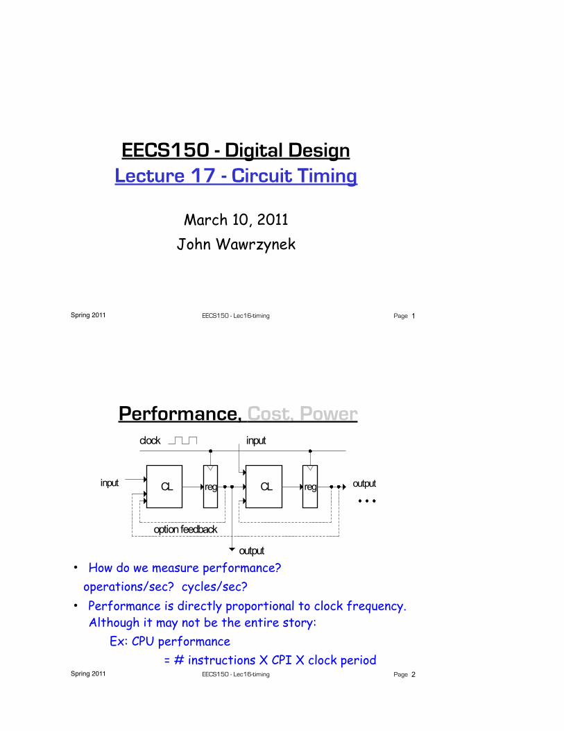
Performance, Cost, Power
• How do we measure performance?operations/sec? cycles/sec?
• Performance is directly proportional to clock frequency. Although it may not be the entire story:
Ex: CPU performance = # instructions X CPI X clock period
2
Spring 2011 EECS150 - Lec16-timing Page
Timing Analysis1600 IEEE JOURNAL OF SOLID-STATE CIRCUITS, VOL. 36, NO. 11, NOVEMBER 2001
Fig. 1. Process SEM cross section.
The process was raised from [1] to limit standby power.
Circuit design and architectural pipelining ensure low voltage
performance and functionality. To further limit standby current
in handheld ASSPs, a longer poly target takes advantage of the
versus dependence and source-to-body bias is used
to electrically limit transistor in standby mode. All core
nMOS and pMOS transistors utilize separate source and bulk
connections to support this. The process includes cobalt disili-
cide gates and diffusions. Low source and drain capacitance, as
well as 3-nm gate-oxide thickness, allow high performance and
low-voltage operation.
III. ARCHITECTURE
The microprocessor contains 32-kB instruction and data
caches as well as an eight-entry coalescing writeback buffer.
The instruction and data cache fill buffers have two and four
entries, respectively. The data cache supports hit-under-miss
operation and lines may be locked to allow SRAM-like oper-
ation. Thirty-two-entry fully associative translation lookaside
buffers (TLBs) that support multiple page sizes are provided
for both caches. TLB entries may also be locked. A 128-entry
branch target buffer improves branch performance a pipeline
deeper than earlier high-performance ARM designs [2], [3].
A. Pipeline Organization
To obtain high performance, the microprocessor core utilizes
a simple scalar pipeline and a high-frequency clock. In addition
to avoiding the potential power waste of a superscalar approach,
functional design and validation complexity is decreased at the
expense of circuit design effort. To avoid circuit design issues,
the pipeline partitioning balances the workload and ensures that
no one pipeline stage is tight. The main integer pipeline is seven
stages, memory operations follow an eight-stage pipeline, and
when operating in thumb mode an extra pipe stage is inserted
after the last fetch stage to convert thumb instructions into ARM
instructions. Since thumb mode instructions [11] are 16 b, two
instructions are fetched in parallel while executing thumb in-
structions. A simplified diagram of the processor pipeline is
Fig. 2. Microprocessor pipeline organization.
shown in Fig. 2, where the state boundaries are indicated by
gray. Features that allow the microarchitecture to achieve high
speed are as follows.
The shifter and ALU reside in separate stages. The ARM in-
struction set allows a shift followed by an ALU operation in a
single instruction. Previous implementations limited frequency
by having the shift and ALU in a single stage. Splitting this op-
eration reduces the critical ALU bypass path by approximately
1/3. The extra pipeline hazard introduced when an instruction is
immediately followed by one requiring that the result be shifted
is infrequent.
Decoupled Instruction Fetch.A two-instruction deep queue is
implemented between the second fetch and instruction decode
pipe stages. This allows stalls generated later in the pipe to be
deferred by one or more cycles in the earlier pipe stages, thereby
allowing instruction fetches to proceed when the pipe is stalled,
and also relieves stall speed paths in the instruction fetch and
branch prediction units.
Deferred register dependency stalls. While register depen-
dencies are checked in the RF stage, stalls due to these hazards
are deferred until the X1 stage. All the necessary operands are
then captured from result-forwarding busses as the results are
returned to the register file.
One of the major goals of the design was to minimize the en-
ergy consumed to complete a given task. Conventional wisdom
has been that shorter pipelines are more efficient due to re-
!"#$%&'())* ++,!-.)'/ 012-)34$5$%& 67&1'8
!"#$%&'
( )#*#&&'&+,-+.'*/#&+0-12'*,'*3+
#
4 5+! ,/$'60&7"89+:+,/$'6$;"9+:+,/$'6.',;%9
5+! #0&7"8 :+#$;" :+#.',;%
0&7
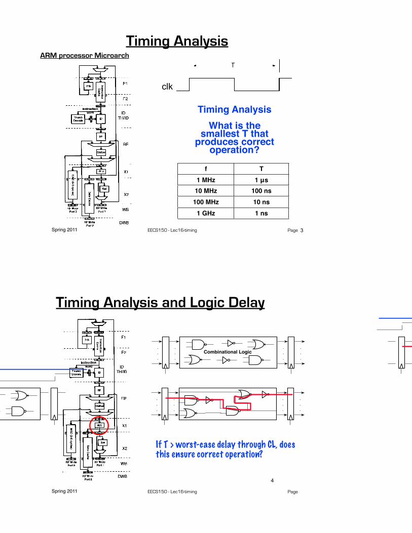
f T1 MHz 1 μs
10 MHz 100 ns100 MHz 10 ns
1 GHz 1 ns
Timing AnalysisWhat is the
smallest T that produces correct
operation?
3
ARM processor Microarch
Spring 2011 EECS150 - Lec16-timing Page
Timing Analysis and Logic Delay
If T > worst-case delay through CL, does this ensure correct operation?
1600 IEEE JOURNAL OF SOLID-STATE CIRCUITS, VOL. 36, NO. 11, NOVEMBER 2001
Fig. 1. Process SEM cross section.
The process was raised from [1] to limit standby power.
Circuit design and architectural pipelining ensure low voltage
performance and functionality. To further limit standby current
in handheld ASSPs, a longer poly target takes advantage of the
versus dependence and source-to-body bias is used
to electrically limit transistor in standby mode. All core
nMOS and pMOS transistors utilize separate source and bulk
connections to support this. The process includes cobalt disili-
cide gates and diffusions. Low source and drain capacitance, as
well as 3-nm gate-oxide thickness, allow high performance and
low-voltage operation.
III. ARCHITECTURE
The microprocessor contains 32-kB instruction and data
caches as well as an eight-entry coalescing writeback buffer.
The instruction and data cache fill buffers have two and four
entries, respectively. The data cache supports hit-under-miss
operation and lines may be locked to allow SRAM-like oper-
ation. Thirty-two-entry fully associative translation lookaside
buffers (TLBs) that support multiple page sizes are provided
for both caches. TLB entries may also be locked. A 128-entry
branch target buffer improves branch performance a pipeline
deeper than earlier high-performance ARM designs [2], [3].
A. Pipeline Organization
To obtain high performance, the microprocessor core utilizes
a simple scalar pipeline and a high-frequency clock. In addition
to avoiding the potential power waste of a superscalar approach,
functional design and validation complexity is decreased at the
expense of circuit design effort. To avoid circuit design issues,
the pipeline partitioning balances the workload and ensures that
no one pipeline stage is tight. The main integer pipeline is seven
stages, memory operations follow an eight-stage pipeline, and
when operating in thumb mode an extra pipe stage is inserted
after the last fetch stage to convert thumb instructions into ARM
instructions. Since thumb mode instructions [11] are 16 b, two
instructions are fetched in parallel while executing thumb in-
structions. A simplified diagram of the processor pipeline is
Fig. 2. Microprocessor pipeline organization.
shown in Fig. 2, where the state boundaries are indicated by
gray. Features that allow the microarchitecture to achieve high
speed are as follows.
The shifter and ALU reside in separate stages. The ARM in-
struction set allows a shift followed by an ALU operation in a
single instruction. Previous implementations limited frequency
by having the shift and ALU in a single stage. Splitting this op-
eration reduces the critical ALU bypass path by approximately
1/3. The extra pipeline hazard introduced when an instruction is
immediately followed by one requiring that the result be shifted
is infrequent.
Decoupled Instruction Fetch.A two-instruction deep queue is
implemented between the second fetch and instruction decode
pipe stages. This allows stalls generated later in the pipe to be
deferred by one or more cycles in the earlier pipe stages, thereby
allowing instruction fetches to proceed when the pipe is stalled,
and also relieves stall speed paths in the instruction fetch and
branch prediction units.
Deferred register dependency stalls. While register depen-
dencies are checked in the RF stage, stalls due to these hazards
are deferred until the X1 stage. All the necessary operands are
then captured from result-forwarding busses as the results are
returned to the register file.
One of the major goals of the design was to minimize the en-
ergy consumed to complete a given task. Conventional wisdom
has been that shorter pipelines are more efficient due to re-
1/28/04 ©UCB Spring 2004CS152 / Kubiatowicz
Lec3.9
General C/L Cell Delay Model
° Combinational Cell (symbol) is fully specified by:• functional (input -> output) behavior
- truth-table, logic equation, VHDL
• Input load factor of each input
• Propagation delay from each input to each output for each transition
- THL(A, o) = Fixed Internal Delay + Load-dependent-delay x load
° Linear model composes
Cout
Vout
Cout
Delay
Va -> Vout
XX
X
X
X
X
Ccritical
delay per unit load
A
B
X
.
.
.
Combinational
Logic Cell
Internal Delay
1/28/04 ©UCB Spring 2004CS152 / Kubiatowicz
Lec3.10
Storage Element’s Timing Model
Clk
D Q
° Setup Time: Input must be stable BEFORE trigger clock edge
° Hold Time: Input must REMAIN stable after trigger clock edge
° Clock-to-Q time:
• Output cannot change instantaneously at the trigger clock edge
• Similar to delay in logic gates, two components:
- Internal Clock-to-Q
- Load dependent Clock-to-Q
Don’t Care Don’t Care
HoldSetup
D
Unknown
Clock-to-Q
Q
1/28/04 ©UCB Spring 2004CS152 / Kubiatowicz
Lec3.11
Clocking Methodology
Clk
Combination Logic
.
.
.
.
.
.
.
.
.
.
.
.
° All storage elements are clocked by the same clock edge
° The combination logic blocks:• Inputs are updated at each clock tick
• All outputs MUST be stable before the next clock tick
1/28/04 ©UCB Spring 2004CS152 / Kubiatowicz
Lec3.12
Critical Path & Cycle Time
Clk
.
.
.
.
.
.
.
.
.
.
.
.
° Critical path: the slowest path between any two storage devices
° Cycle time is a function of the critical path
° must be greater than:
Clock-to-Q + Longest Path through Combination Logic + Setup
1/28/04 ©UCB Spring 2004CS152 / Kubiatowicz
Lec3.9
General C/L Cell Delay Model
° Combinational Cell (symbol) is fully specified by:• functional (input -> output) behavior
- truth-table, logic equation, VHDL
• Input load factor of each input
• Propagation delay from each input to each output for each transition
- THL(A, o) = Fixed Internal Delay + Load-dependent-delay x load
° Linear model composes
Cout
Vout
Cout
Delay
Va -> Vout
XX
X
X
X
X
Ccritical
delay per unit load
A
B
X
.
.
.
Combinational
Logic Cell
Internal Delay
1/28/04 ©UCB Spring 2004CS152 / Kubiatowicz
Lec3.10
Storage Element’s Timing Model
Clk
D Q
° Setup Time: Input must be stable BEFORE trigger clock edge
° Hold Time: Input must REMAIN stable after trigger clock edge
° Clock-to-Q time:
• Output cannot change instantaneously at the trigger clock edge
• Similar to delay in logic gates, two components:
- Internal Clock-to-Q
- Load dependent Clock-to-Q
Don’t Care Don’t Care
HoldSetup
D
Unknown
Clock-to-Q
Q
1/28/04 ©UCB Spring 2004CS152 / Kubiatowicz
Lec3.11
Clocking Methodology
Clk
Combination Logic
.
.
.
.
.
.
.
.
.
.
.
.
° All storage elements are clocked by the same clock edge
° The combination logic blocks:• Inputs are updated at each clock tick
• All outputs MUST be stable before the next clock tick
1/28/04 ©UCB Spring 2004CS152 / Kubiatowicz
Lec3.12
Critical Path & Cycle Time
Clk
.
.
.
.
.
.
.
.
.
.
.
.
° Critical path: the slowest path between any two storage devices
° Cycle time is a function of the critical path
° must be greater than:
Clock-to-Q + Longest Path through Combination Logic + Setup
Combinational Logic
4

Spring 2011 EECS150 - Lec16-timing Page
Limitations on Clock Rate
1 Logic Gate Delay 2 Delays in flip-flops
• What must happen in one clock cycle for correct operation?– All signals connected to FF (or memory) inputs must be
ready and “setup” before rising edge of clock. – For now we assume perfect clock distribution (all flip-flops
see the clock at the same time).5
What are typical delay values?Both times contribute to limiting the clock period.
Spring 2011 EECS150 - Lec16-timing Page
Example
Parallel to serial converter circuit
T ≥ time(clk→Q) + time(mux) + time(setup)T ≥ τclk→Q + τmux + τsetupa
b
clk
6
Spring 2011 EECS150 - Lec16-timing Page
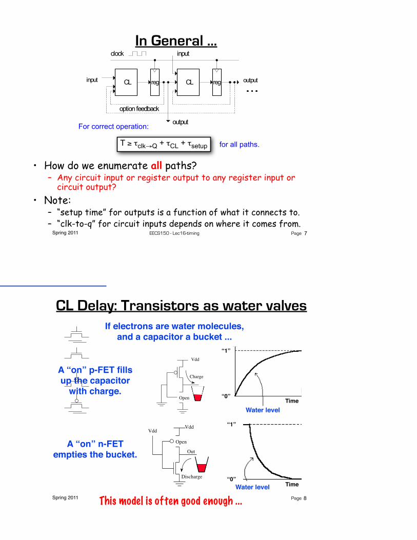
In General ...
T ≥ τclk→Q + τCL + τsetup
7
For correct operation:
for all paths.
• How do we enumerate all paths?– Any circuit input or register output to any register input or
circuit output?• Note:
– “setup time” for outputs is a function of what it connects to.– “clk-to-q” for circuit inputs depends on where it comes from.
Spring 2011 EECS150 - Lec16-timing Page
CL Delay: Transistors as water valvesIf electrons are water molecules,
and a capacitor a bucket ...
A “on” p-FET fillsup the capacitor
with charge.
1/28/04 ©UCB Spring 2004CS152 / Kubiatowicz
Lec3.29
Delay Model:
CMOS
1/28/04 ©UCB Spring 2004CS152 / Kubiatowicz
Lec3.30
Review: General C/L Cell Delay Model
° Combinational Cell (symbol) is fully specified by:• functional (input -> output) behavior
- truth-table, logic equation, VHDL
• load factor of each input
• critical propagation delay from each input to each output for each transition
- THL(A, o) = Fixed Internal Delay + Load-dependent-delay x load
° Linear model composes
Cout
Vout
Cout
Delay
Va -> Vout
XX
X
X
X
X
Ccritical
delay per unit load
A
B
X
.
.
.
Combinational
Logic Cell
Internal Delay
1/28/04 ©UCB Spring 2004CS152 / Kubiatowicz
Lec3.31
Basic Technology: CMOS
° CMOS: Complementary Metal Oxide Semiconductor• NMOS (N-Type Metal Oxide Semiconductor) transistors
• PMOS (P-Type Metal Oxide Semiconductor) transistors
° NMOS Transistor• Apply a HIGH (Vdd) to its gate
turns the transistor into a “conductor”
• Apply a LOW (GND) to its gateshuts off the conduction path
° PMOS Transistor• Apply a HIGH (Vdd) to its gate
shuts off the conduction path
• Apply a LOW (GND) to its gateturns the transistor into a “conductor”
Vdd = 5V
GND = 0v
Vdd = 5V
GND = 0v
1/28/04 ©UCB Spring 2004CS152 / Kubiatowicz
Lec3.32
Basic Components: CMOS Inverter
Vdd
Circuit
° Inverter Operation
OutIn
SymbolPMOS
NMOS
In Out
Vdd
Open
Charge
VoutVdd
Vdd
Out
Open
Discharge
Vin
Vdd
Vdd
A “on” n-FET empties the bucket.
1/28/04 ©UCB Spring 2004CS152 / Kubiatowicz
Lec3.29
Delay Model:
CMOS
1/28/04 ©UCB Spring 2004CS152 / Kubiatowicz
Lec3.30
Review: General C/L Cell Delay Model
° Combinational Cell (symbol) is fully specified by:• functional (input -> output) behavior
- truth-table, logic equation, VHDL
• load factor of each input
• critical propagation delay from each input to each output for each transition
- THL(A, o) = Fixed Internal Delay + Load-dependent-delay x load
° Linear model composes
Cout
Vout
Cout
Delay
Va -> Vout
XX
X
X
X
X
Ccritical
delay per unit load
A
B
X
.
.
.
Combinational
Logic Cell
Internal Delay
1/28/04 ©UCB Spring 2004CS152 / Kubiatowicz
Lec3.31
Basic Technology: CMOS
° CMOS: Complementary Metal Oxide Semiconductor• NMOS (N-Type Metal Oxide Semiconductor) transistors
• PMOS (P-Type Metal Oxide Semiconductor) transistors
° NMOS Transistor• Apply a HIGH (Vdd) to its gate
turns the transistor into a “conductor”
• Apply a LOW (GND) to its gateshuts off the conduction path
° PMOS Transistor• Apply a HIGH (Vdd) to its gate
shuts off the conduction path
• Apply a LOW (GND) to its gateturns the transistor into a “conductor”
Vdd = 5V
GND = 0v
Vdd = 5V
GND = 0v
1/28/04 ©UCB Spring 2004CS152 / Kubiatowicz
Lec3.32
Basic Components: CMOS Inverter
Vdd
Circuit
° Inverter Operation
OutIn
SymbolPMOS
NMOS
In Out
Vdd
Open
Charge
VoutVdd
Vdd
Out
Open
Discharge
Vin
Vdd
Vdd
!"#$%&'())* ++,!-.)'/ 012-)34$5$%& 67&1'-)
!"#$%&'(#)*(+,%-$*".(/0
1 2+.$0#$03
1 4546%,"#$3
“1”
“0”Time
Water level
!"#$%&'())* ++,!-.)'/ 012-)34$5$%& 67&1'-)
!"#$%&'(#)*(+,%-$*".(/0
1 2+.$0#$03
1 4546%,"#$3
“0”
“1”
TimeWater level
This model is often good enough ... 8
Spring 2011 EECS150 - Lec16-timing Page
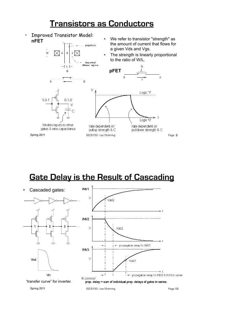
Transistors as Conductors• Improved Transistor Model:
nFET • We refer to transistor "strength" as the amount of current that flows for a given Vds and Vgs.
• The strength is linearly proportional to the ratio of W/L.
pFET
9
Spring 2011 EECS150 - Lec16-timing Page
Gate Delay is the Result of Cascading• Cascaded gates:
“transfer curve” for inverter.
10
Spring 2011 EECS150 - Lec16-timing Page
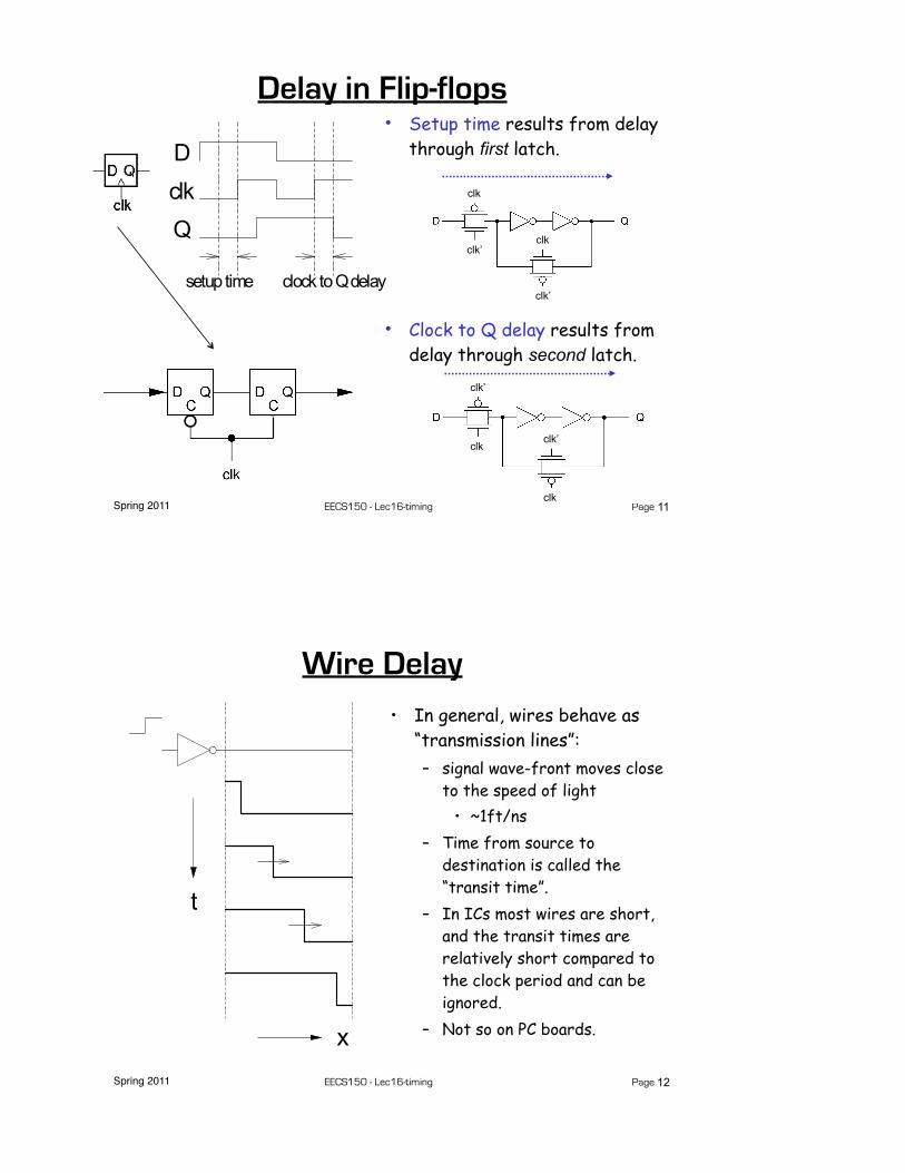
Delay in Flip-flops• Setup time results from delay
through first latch.
• Clock to Q delay results from delay through second latch.
clk
clk’
clk
clk’
clk
clk’
clk
clk’
11
Spring 2011 EECS150 - Lec16-timing Page
Wire Delay• In general, wires behave as
“transmission lines”:– signal wave-front moves close
to the speed of light• ~1ft/ns
– Time from source to destination is called the “transit time”.
– In ICs most wires are short, and the transit times are relatively short compared to the clock period and can be ignored.
– Not so on PC boards.
12

Spring 2011 EECS150 - Lec16-timing Page
Wire Delay• Even in those cases where the
transmission line effect is negligible:– Wires posses distributed
resistance and capacitance
– Time constant associated with distributed RC is proportional to the square of the length
• For short wires on ICs, resistance is insignificant (relative to effective R of transistors), but C is important.– Typically around half of C of
gate load is in the wires.• For long wires on ICs:
– busses, clock lines, global control signal, etc.
– Resistance is significant, therefore distributed RC effect dominates.
– signals are typically “rebuffered” to reduce delay:
v1 v2 v3 v4
13
v1
v4v3
v2
time
Spring 2011 EECS150 - Lec16-timing Page
Delay and “Fan-out”
• The delay of a gate is proportional to its output capacitance. Connecting the output of gate one increases it’s output capacitance. Therefore, it takes increasingly longer for the output of a gate to reach the switching threshold of the gates it drives as we add more output connections.
• Driving wires also contributes to fan-out delay.• What can be done to remedy this problem in large fan-out situations?
1
3
2
14

Spring 2011 EECS150 - Lec16-timing Page
“Critical” Path
• Critical Path: the path in the entire design with the maximum delay.– This could be from state element to state element, or from
input to state element, or state element to output, or from input to output (unregistered paths).
• For example, what is the critical path in this circuit?
• Why do we care about the critical path?
15
Spring 2011 EECS150 - Lec16-timing Page
Searching for processor critical path1600 IEEE JOURNAL OF SOLID-STATE CIRCUITS, VOL. 36, NO. 11, NOVEMBER 2001
Fig. 1. Process SEM cross section.
The process was raised from [1] to limit standby power.
Circuit design and architectural pipelining ensure low voltage
performance and functionality. To further limit standby current
in handheld ASSPs, a longer poly target takes advantage of the
versus dependence and source-to-body bias is used
to electrically limit transistor in standby mode. All core
nMOS and pMOS transistors utilize separate source and bulk
connections to support this. The process includes cobalt disili-
cide gates and diffusions. Low source and drain capacitance, as
well as 3-nm gate-oxide thickness, allow high performance and
low-voltage operation.
III. ARCHITECTURE
The microprocessor contains 32-kB instruction and data
caches as well as an eight-entry coalescing writeback buffer.
The instruction and data cache fill buffers have two and four
entries, respectively. The data cache supports hit-under-miss
operation and lines may be locked to allow SRAM-like oper-
ation. Thirty-two-entry fully associative translation lookaside
buffers (TLBs) that support multiple page sizes are provided
for both caches. TLB entries may also be locked. A 128-entry
branch target buffer improves branch performance a pipeline
deeper than earlier high-performance ARM designs [2], [3].
A. Pipeline Organization
To obtain high performance, the microprocessor core utilizes
a simple scalar pipeline and a high-frequency clock. In addition
to avoiding the potential power waste of a superscalar approach,
functional design and validation complexity is decreased at the
expense of circuit design effort. To avoid circuit design issues,
the pipeline partitioning balances the workload and ensures that
no one pipeline stage is tight. The main integer pipeline is seven
stages, memory operations follow an eight-stage pipeline, and
when operating in thumb mode an extra pipe stage is inserted
after the last fetch stage to convert thumb instructions into ARM
instructions. Since thumb mode instructions [11] are 16 b, two
instructions are fetched in parallel while executing thumb in-
structions. A simplified diagram of the processor pipeline is
Fig. 2. Microprocessor pipeline organization.
shown in Fig. 2, where the state boundaries are indicated by
gray. Features that allow the microarchitecture to achieve high
speed are as follows.
The shifter and ALU reside in separate stages. The ARM in-
struction set allows a shift followed by an ALU operation in a
single instruction. Previous implementations limited frequency
by having the shift and ALU in a single stage. Splitting this op-
eration reduces the critical ALU bypass path by approximately
1/3. The extra pipeline hazard introduced when an instruction is
immediately followed by one requiring that the result be shifted
is infrequent.
Decoupled Instruction Fetch.A two-instruction deep queue is
implemented between the second fetch and instruction decode
pipe stages. This allows stalls generated later in the pipe to be
deferred by one or more cycles in the earlier pipe stages, thereby
allowing instruction fetches to proceed when the pipe is stalled,
and also relieves stall speed paths in the instruction fetch and
branch prediction units.
Deferred register dependency stalls. While register depen-
dencies are checked in the RF stage, stalls due to these hazards
are deferred until the X1 stage. All the necessary operands are
then captured from result-forwarding busses as the results are
returned to the register file.
One of the major goals of the design was to minimize the en-
ergy consumed to complete a given task. Conventional wisdom
has been that shorter pipelines are more efficient due to re-
Must consider all connected register pairs, paths from input to register, register to output. Don’t forget the controller.
?
16
• Design tools help in the search. – Synthesis tools report delays on paths, – Special static timing analyzers accept
a design netlist and report path delays, – and, of course, simulators can be used
to determine timing performance.
Tools that are expected to do something about the timing behavior (such as synthesizers), also include provisions for specifying input arrival times (relative to the clock), and output requirements (set-up times of next stage).
Spring 2011 EECS150 - Lec16-timing Page
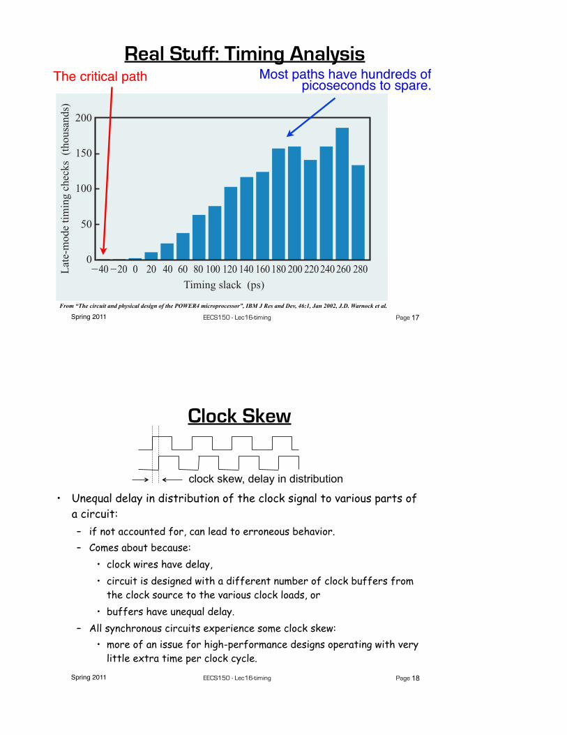
Real Stuff: Timing Analysis
From “The circuit and physical design of the POWER4 microprocessor”, IBM J Res and Dev, 46:1, Jan 2002, J.D. Warnock et al.
netlist. Of these, 121 713 were top-level chip global nets,and 21 711 were processor-core-level global nets. Againstthis model 3.5 million setup checks were performed in latemode at points where clock signals met data signals inlatches or dynamic circuits. The total number of timingchecks of all types performed in each chip run was9.8 million. Depending on the configuration of the timingrun and the mix of actual versus estimated design data,the amount of real memory required was in the rangeof 12 GB to 14 GB, with run times of about 5 to 6 hoursto the start of timing-report generation on an RS/6000*Model S80 configured with 64 GB of real memory.Approximately half of this time was taken up by readingin the netlist, timing rules, and extracted RC networks, as
well as building and initializing the internal data structuresfor the timing model. The actual static timing analysistypically took 2.5–3 hours. Generation of the entirecomplement of reports and analysis required an additional5 to 6 hours to complete. A total of 1.9 GB of timingreports and analysis were generated from each chip timingrun. This data was broken down, analyzed, and organizedby processor core and GPS, individual unit, and, in thecase of timing contracts, by unit and macro. This was onecomponent of the 24-hour-turnaround time achieved forthe chip-integration design cycle. Figure 26 shows theresults of iterating this process: A histogram of the finalnominal path delays obtained from static timing for thePOWER4 processor.
The POWER4 design includes LBIST and ABIST(Logic/Array Built-In Self-Test) capability to enable full-frequency ac testing of the logic and arrays. Such testingon pre-final POWER4 chips revealed that several circuitmacros ran slower than predicted from static timing. Thespeed of the critical paths in these macros was increasedin the final design. Typical fast ac LBIST laboratory testresults measured on POWER4 after these paths wereimproved are shown in Figure 27.
SummaryThe 174-million-transistor !1.3-GHz POWER4 chip,containing two microprocessor cores and an on-chipmemory subsystem, is a large, complex, high-frequencychip designed by a multi-site design team. Theperformance and schedule goals set at the beginning ofthe project were met successfully. This paper describesthe circuit and physical design of POWER4, emphasizingaspects that were important to the project’s success in theareas of design methodology, clock distribution, circuits,power, integration, and timing.
Figure 25
POWER4 timing flow. This process was iterated daily during the physical design phase to close timing.
VIM
Timer files ReportsAsserts
Spice
Spice
GL/1
Reports
< 12 hr
< 12 hr
< 12 hr
< 48 hr
< 24 hr
Non-uplift timing
Noiseimpacton timing
Upliftanalysis
Capacitanceadjust
Chipbench /EinsTimer
Chipbench /EinsTimer
Extraction
Core or chipwiring
Analysis/update(wires, buffers)
Notes:• Executed 2–3 months prior to tape-out• Fully extracted data from routed designs • Hierarchical extraction• Custom logic handled separately • Dracula • Harmony• Extraction done for • Early • Late
Extracted units (flat or hierarchical)Incrementally extracted RLMsCustom NDRsVIMs
Figure 26
Histogram of the POWER4 processor path delays.
!40 !20 0 20 40 60 80 100 120 140 160 180 200 220 240 260 280Timing slack (ps)
Lat
e-m
ode
timin
g ch
ecks
(th
ousa
nds)
0
50
100
150
200
IBM J. RES. & DEV. VOL. 46 NO. 1 JANUARY 2002 J. D. WARNOCK ET AL.
47
Most paths have hundreds of picoseconds to spare.The critical path
17
Spring 2011 EECS150 - Lec16-timing Page
Clock Skew
• Unequal delay in distribution of the clock signal to various parts of a circuit:– if not accounted for, can lead to erroneous behavior.– Comes about because:
• clock wires have delay,• circuit is designed with a different number of clock buffers from
the clock source to the various clock loads, or• buffers have unequal delay.
– All synchronous circuits experience some clock skew:• more of an issue for high-performance designs operating with very
little extra time per clock cycle.
clock skew, delay in distribution
18

Spring 2011 EECS150 - Lec16-timing Page
Clock Skew (cont.)
• If clock period T = TCL+Tsetup+Tclk→Q, circuit will fail.
• Therefore:1. Control clock skew a) Careful clock distribution. Equalize path delay from clock source to
all clock loads by controlling wires delay and buffer delay. b) don’t “gate” clocks in a non-uniform way.2. T ≥ TCL+Tsetup+Tclk→Q + worst case skew.
• Most modern large high-performance chips (microprocessors) control end to end clock skew to a small fraction of the clock period.
clock skew, delay in distributionCL
CLKCLK’
CLK
CLK’
19
Spring 2011 EECS150 - Lec16-timing Page
Clock Skew (cont.)
• Note reversed buffer.• In this case, clock skew actually provides extra time (adds to
the effective clock period).• This effect has been used to help run circuits as higher
clock rates. Risky business!
CL
CLKCLK’
clock skew, delay in distribution
CLK
CLK’
20
Spring 2011 EECS150 - Lec16-timing Page
1600 IEEE JOURNAL OF SOLID-STATE CIRCUITS, VOL. 36, NO. 11, NOVEMBER 2001
Fig. 1. Process SEM cross section.
The process was raised from [1] to limit standby power.
Circuit design and architectural pipelining ensure low voltage
performance and functionality. To further limit standby current
in handheld ASSPs, a longer poly target takes advantage of the
versus dependence and source-to-body bias is used
to electrically limit transistor in standby mode. All core
nMOS and pMOS transistors utilize separate source and bulk
connections to support this. The process includes cobalt disili-
cide gates and diffusions. Low source and drain capacitance, as
well as 3-nm gate-oxide thickness, allow high performance and
low-voltage operation.
III. ARCHITECTURE
The microprocessor contains 32-kB instruction and data
caches as well as an eight-entry coalescing writeback buffer.
The instruction and data cache fill buffers have two and four
entries, respectively. The data cache supports hit-under-miss
operation and lines may be locked to allow SRAM-like oper-
ation. Thirty-two-entry fully associative translation lookaside
buffers (TLBs) that support multiple page sizes are provided
for both caches. TLB entries may also be locked. A 128-entry
branch target buffer improves branch performance a pipeline
deeper than earlier high-performance ARM designs [2], [3].
A. Pipeline Organization
To obtain high performance, the microprocessor core utilizes
a simple scalar pipeline and a high-frequency clock. In addition
to avoiding the potential power waste of a superscalar approach,
functional design and validation complexity is decreased at the
expense of circuit design effort. To avoid circuit design issues,
the pipeline partitioning balances the workload and ensures that
no one pipeline stage is tight. The main integer pipeline is seven
stages, memory operations follow an eight-stage pipeline, and
when operating in thumb mode an extra pipe stage is inserted
after the last fetch stage to convert thumb instructions into ARM
instructions. Since thumb mode instructions [11] are 16 b, two
instructions are fetched in parallel while executing thumb in-
structions. A simplified diagram of the processor pipeline is
Fig. 2. Microprocessor pipeline organization.
shown in Fig. 2, where the state boundaries are indicated by
gray. Features that allow the microarchitecture to achieve high
speed are as follows.
The shifter and ALU reside in separate stages. The ARM in-
struction set allows a shift followed by an ALU operation in a
single instruction. Previous implementations limited frequency
by having the shift and ALU in a single stage. Splitting this op-
eration reduces the critical ALU bypass path by approximately
1/3. The extra pipeline hazard introduced when an instruction is
immediately followed by one requiring that the result be shifted
is infrequent.
Decoupled Instruction Fetch.A two-instruction deep queue is
implemented between the second fetch and instruction decode
pipe stages. This allows stalls generated later in the pipe to be
deferred by one or more cycles in the earlier pipe stages, thereby
allowing instruction fetches to proceed when the pipe is stalled,
and also relieves stall speed paths in the instruction fetch and
branch prediction units.
Deferred register dependency stalls. While register depen-
dencies are checked in the RF stage, stalls due to these hazards
are deferred until the X1 stage. All the necessary operands are
then captured from result-forwarding busses as the results are
returned to the register file.
One of the major goals of the design was to minimize the en-
ergy consumed to complete a given task. Conventional wisdom
has been that shorter pipelines are more efficient due to re-
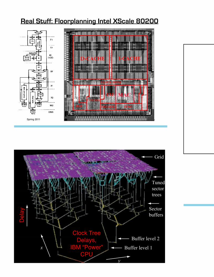
Real Stuff: Floorplanning Intel XScale 80200
21
Spring 2011 EECS150 - Lec16-timing Page
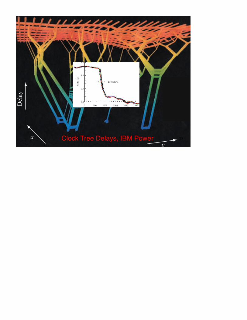
the total wire delay is similar to the total buffer delay. Apatented tuning algorithm [16] was required to tune themore than 2000 tunable transmission lines in these sectortrees to achieve low skew, visualized as the flatness of thegrid in the 3D visualizations. Figure 8 visualizes four ofthe 64 sector trees containing about 125 tuned wiresdriving 1/16th of the clock grid. While symmetric H-treeswere desired, silicon and wiring blockages often forcedmore complex tree structures, as shown. Figure 8 alsoshows how the longer wires are split into multiple-fingeredtransmission lines interspersed with Vdd and ground shields(not shown) for better inductance control [17, 18]. Thisstrategy of tunable trees driving a single grid results in lowskew among any of the 15 200 clock pins on the chip,regardless of proximity.
From the global clock grid, a hierarchy of short clockroutes completed the connection from the grid down tothe individual local clock buffer inputs in the macros.These clock routing segments included wires at the macrolevel from the macro clock pins to the input of the localclock buffer, wires at the unit level from the macro clockpins to the unit clock pins, and wires at the chip levelfrom the unit clock pins to the clock grid.
Design methodology and resultsThis clock-distribution design method allows a highlyproductive combination of top-down and bottom-up designperspectives, proceeding in parallel and meeting at thesingle clock grid, which is designed very early. The treesdriving the grid are designed top-down, with the maximumwire widths contracted for them. Once the contract for thegrid had been determined, designers were insulated fromchanges to the grid, allowing necessary adjustments to thegrid to be made for minimizing clock skew even at a verylate stage in the design process. The macro, unit, and chipclock wiring proceeded bottom-up, with point tools ateach hierarchical level (e.g., macro, unit, core, and chip)using contracted wiring to form each segment of the totalclock wiring. At the macro level, short clock routesconnected the macro clock pins to the local clock buffers.These wires were kept very short, and duplication ofexisting higher-level clock routes was avoided by allowingthe use of multiple clock pins. At the unit level, clockrouting was handled by a special tool, which connected themacro pins to unit-level pins, placed as needed in pre-assigned wiring tracks. The final connection to the fixed
Figure 6
Schematic diagram of global clock generation and distribution.
PLL
Bypass
Referenceclock in
Referenceclock out
Clock distributionClock out
Figure 7
3D visualization of the entire global clock network. The x and y coordinates are chip x, y, while the z axis is used to represent delay, so the lowest point corresponds to the beginning of the clock distribution and the final clock grid is at the top. Widths are proportional to tuned wire width, and the three levels of buffers appear as vertical lines.
Del
ay
Grid
Tunedsectortrees
Sectorbuffers
Buffer level 2
Buffer level 1
y
x
Figure 8
Visualization of four of the 64 sector trees driving the clock grid, using the same representation as Figure 7. The complex sector trees and multiple-fingered transmission lines used for inductance control are visible at this scale.
Del
ay Multiple-fingeredtransmissionline
yx
J. D. WARNOCK ET AL. IBM J. RES. & DEV. VOL. 46 NO. 1 JANUARY 2002
32
Clock Tree Delays,
IBM “Power” CPU
Del
ay
22
Spring 2011 EECS150 - Lec16-timing Page
the total wire delay is similar to the total buffer delay. Apatented tuning algorithm [16] was required to tune themore than 2000 tunable transmission lines in these sectortrees to achieve low skew, visualized as the flatness of thegrid in the 3D visualizations. Figure 8 visualizes four ofthe 64 sector trees containing about 125 tuned wiresdriving 1/16th of the clock grid. While symmetric H-treeswere desired, silicon and wiring blockages often forcedmore complex tree structures, as shown. Figure 8 alsoshows how the longer wires are split into multiple-fingeredtransmission lines interspersed with Vdd and ground shields(not shown) for better inductance control [17, 18]. Thisstrategy of tunable trees driving a single grid results in lowskew among any of the 15 200 clock pins on the chip,regardless of proximity.
From the global clock grid, a hierarchy of short clockroutes completed the connection from the grid down tothe individual local clock buffer inputs in the macros.These clock routing segments included wires at the macrolevel from the macro clock pins to the input of the localclock buffer, wires at the unit level from the macro clockpins to the unit clock pins, and wires at the chip levelfrom the unit clock pins to the clock grid.
Design methodology and resultsThis clock-distribution design method allows a highlyproductive combination of top-down and bottom-up designperspectives, proceeding in parallel and meeting at thesingle clock grid, which is designed very early. The treesdriving the grid are designed top-down, with the maximumwire widths contracted for them. Once the contract for thegrid had been determined, designers were insulated fromchanges to the grid, allowing necessary adjustments to thegrid to be made for minimizing clock skew even at a verylate stage in the design process. The macro, unit, and chipclock wiring proceeded bottom-up, with point tools ateach hierarchical level (e.g., macro, unit, core, and chip)using contracted wiring to form each segment of the totalclock wiring. At the macro level, short clock routesconnected the macro clock pins to the local clock buffers.These wires were kept very short, and duplication ofexisting higher-level clock routes was avoided by allowingthe use of multiple clock pins. At the unit level, clockrouting was handled by a special tool, which connected themacro pins to unit-level pins, placed as needed in pre-assigned wiring tracks. The final connection to the fixed
Figure 6
Schematic diagram of global clock generation and distribution.
PLL
Bypass
Referenceclock in
Referenceclock out
Clock distributionClock out
Figure 7
3D visualization of the entire global clock network. The x and y coordinates are chip x, y, while the z axis is used to represent delay, so the lowest point corresponds to the beginning of the clock distribution and the final clock grid is at the top. Widths are proportional to tuned wire width, and the three levels of buffers appear as vertical lines.
Del
ay
Grid
Tunedsectortrees
Sectorbuffers
Buffer level 2
Buffer level 1
y
x
Figure 8
Visualization of four of the 64 sector trees driving the clock grid, using the same representation as Figure 7. The complex sector trees and multiple-fingered transmission lines used for inductance control are visible at this scale.
Del
ay Multiple-fingeredtransmissionline
yx
J. D. WARNOCK ET AL. IBM J. RES. & DEV. VOL. 46 NO. 1 JANUARY 2002
32
Clock Tree Delays, IBM Power
clock grid was completed with a tool run at the chip level,connecting unit-level pins to the grid. At this point, theclock tuning and the bottom-up clock routing process stillhave a great deal of flexibility to respond rapidly to evenlate changes. Repeated practice routing and tuning wereperformed by a small, focused global clock team as theclock pins and buffer placements evolved to guaranteefeasibility and speed the design process.
Measurements of jitter and skew can be carried outusing the I/Os on the chip. In addition, approximately 100top-metal probe pads were included for direct probingof the global clock grid and buffers. Results on actualPOWER4 microprocessor chips show long-distanceskews ranging from 20 ps to 40 ps (cf. Figure 9). This isimproved from early test-chip hardware, which showedas much as 70 ps skew from across-chip channel-lengthvariations [19]. Detailed waveforms at the input andoutput of each global clock buffer were also measuredand compared with simulation to verify the specializedmodeling used to design the clock grid. Good agreementwas found. Thus, we have achieved a “correct-by-design”clock-distribution methodology. It is based on our designexperience and measurements from a series of increasinglyfast, complex server microprocessors. This method resultsin a high-quality global clock without having to usefeedback or adjustment circuitry to control skews.
Circuit designThe cycle-time target for the processor was set early in theproject and played a fundamental role in defining thepipeline structure and shaping all aspects of the circuitdesign as implementation proceeded. Early on, criticaltiming paths through the processor were simulated indetail in order to verify the feasibility of the designpoint and to help structure the pipeline for maximumperformance. Based on this early work, the goal for therest of the circuit design was to match the performance setduring these early studies, with custom design techniquesfor most of the dataflow macros and logic synthesis formost of the control logic—an approach similar to thatused previously [20]. Special circuit-analysis and modelingtechniques were used throughout the design in order toallow full exploitation of all of the benefits of the IBMadvanced SOI technology.
The sheer size of the chip, its complexity, and thenumber of transistors placed some important constraintson the design which could not be ignored in the push tomeet the aggressive cycle-time target on schedule. Theseconstraints led to the adoption of a primarily static-circuitdesign strategy, with dynamic circuits used only sparinglyin SRAMs and other critical regions of the processor core.Power dissipation was a significant concern, and it was akey factor in the decision to adopt a predominantly static-circuit design approach. In addition, the SOI technology,
including uncertainties associated with the modelingof the floating-body effect [21–23] and its impact onnoise immunity [22, 24 –27] and overall chip decouplingcapacitance requirements [26], was another factor behindthe choice of a primarily static design style. Finally, thesize and logical complexity of the chip posed risks tomeeting the schedule; choosing a simple, robust circuitstyle helped to minimize overall risk to the projectschedule with most efficient use of CAD tool and designresources. The size and complexity of the chip alsorequired rigorous testability guidelines, requiring almostall cycle boundary latches to be LSSD-compatible formaximum dc and ac test coverage.
Another important circuit design constraint was thelimit placed on signal slew rates. A global slew rate limitequal to one third of the cycle time was set and enforcedfor all signals (local and global) across the whole chip.The goal was to ensure a robust design, minimizingthe effects of coupled noise on chip timing and alsominimizing the effects of wiring-process variability onoverall path delay. Nets with poor slew also were foundto be more sensitive to device process variations andmodeling uncertainties, even where long wires and RCdelays were not significant factors. The general philosophywas that chip cycle-time goals also had to include theslew-limit targets; it was understood from the beginningthat the real hardware would function at the desiredcycle time only if the slew-limit targets were also met.
The following sections describe how these designconstraints were met without sacrificing cycle time. Thelatch design is described first, including a description ofthe local clocking scheme and clock controls. Then thecircuit design styles are discussed, including a description
Figure 9
Global clock waveforms showing 20 ps of measured skew.
1.5
1.0
0.5
0.0
0 500 1000 1500 2000 2500
20 ps skew
Vol
ts (
V)
Time (ps)
IBM J. RES. & DEV. VOL. 46 NO. 1 JANUARY 2002 J. D. WARNOCK ET AL.
33
23