
Lecture 15: Emotion and Motivation - MIT OpenCourseWare · PDF fileLecture 15: Emotion and Motivation

EE251: Thursday October 12
• Analog to Digital Conversion Continued
– Successive Approximation Method Continued
• Computations
– TM4C A/D Capability and Programming
• Homework #4 due tomorrow
• Lab #5 (A/D Converter) one week lab next week
– Partner with another in this and future labs
Lecture #16 1

Successive Approximation Example
Choose a voltage between 0 and 4 volts: 2.1
4
3
2
1
0
1 2 3 4 5 6 . . . Approximation Number
Voltage
Lecture #16 2
1
0
0
0 0 1
2.0
3.0
2.5
2.25 2.125
2.0625
2.1250 2.09375
A/D Output = 2_100001 = 0x21 = 33
Vmin-max = 4*((33+½))/0x40
= 2.09375 volts

Live Successive Approximation Example
Choose a voltage between 0 and 4 volts: _________
4
3
2
1
0
1 2 3 4 5 6 . . . Approximation Number
Voltage
Lecture #16 3
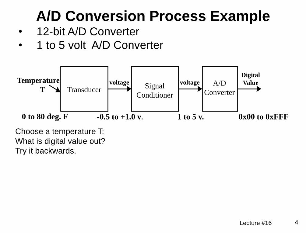
Transducer
Temperature
T Signal
Conditioner
voltage voltage A/D
Converter
Digital
Value
A/D Conversion Process Example • 12-bit A/D Converter
• 1 to 5 volt A/D Converter
Lecture #16 4
0 to 80 deg. F -0.5 to +1.0 v. 1 to 5 v. 0x00 to 0xFFF
Choose a temperature T:
What is digital value out?
Try it backwards.
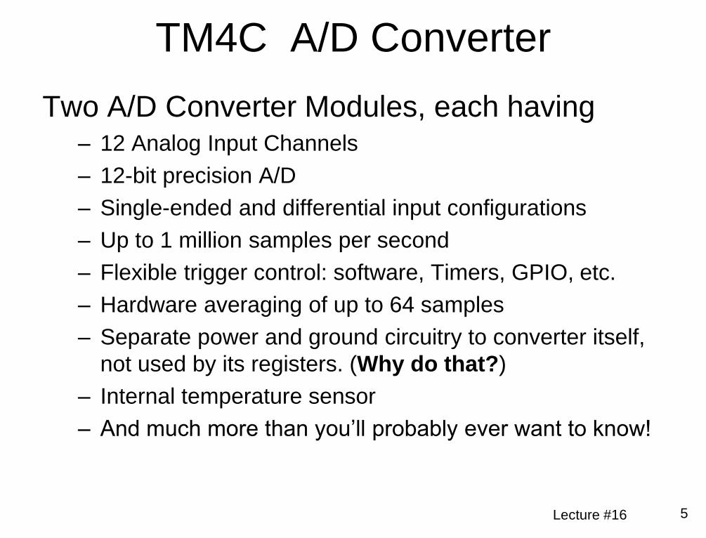
TM4C A/D Converter
Two A/D Converter Modules, each having – 12 Analog Input Channels
– 12-bit precision A/D
– Single-ended and differential input configurations
– Up to 1 million samples per second
– Flexible trigger control: software, Timers, GPIO, etc.
– Hardware averaging of up to 64 samples
– Separate power and ground circuitry to converter itself,
not used by its registers. (Why do that?)
– Internal temperature sensor
– And much more than you’ll probably ever want to know!
Lecture #16 5

TM4C A/D Block Diagram
Lecture #16 6

A/D Input Uses these GPIO Pins (Both Converter Modules Share the Same Pins)
GPIO PIN A/D In
PB4 10
PB5 11
PD0 7
PD1 6
PD2 5
PD3 4
PE0 3
PE1 2
PE2 1
PE3 0
PE4 9
PE5 8
Twelve different pins can be used to do
12 independent analog conversions.
Lecture #16 7

Some Key TM4C A/D Registers (ADC0)
Address 31-2 1 0 Name
$400F.E638 ADC1 ADC0 SYSCTL_RCGCADC_R
31-14 13-12 11-10 9-8 7-6 5-4 3-2 1-0
$4003.8020 SS3 SS2 SS1 SS0 ADC0_SSPRI_R
31-16 15-12 11-8 7-4 3-0
$4003.8014 EM3 EM2 EM1 EM0 ADC0_EMUX_R
31-4 3 2 1 0
$4003.8000 ASEN3 ASEN2 ASEN1 ASEN0 ADC0_ACTSS_R
$4003.80A0 MUX0 ADC0_SSMUX3_R
$4003.80A4 TS0 IE0 END0 D0 ADC0_SSCTL3_R
$4003.8028 SS3 SS2 SS1 SS0 ADC0_PSSI_R
$4003.8004 INR3 INR2 INR1 INR0 ADC0_RIS_R
$4003.8008 MASK3 MASK2 MASK1 MASK0 ADC0_IM_R
$4003.8FC4 Speed ADC0_PC_R
31-12 11-0
$4003.80A8 DATA ADC0_SSFIFO3_R
Register
Name
Important
Bits
Register
Memory
Address
Lecture #16 8
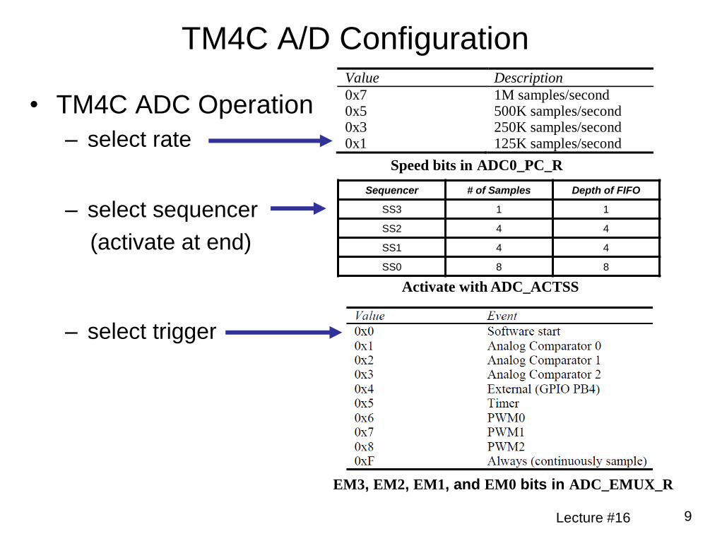
Value Description
0x7 1M samples/second 0x5 500K samples/second 0x3 250K samples/second 0x1 125K samples/second
TM4C A/D Configuration
• TM4C ADC Operation
– select rate
– select sequencer
(activate at end)
– select trigger
Speed bits in ADC0_PC_R
EM3, EM2, EM1, and EM0 bits in ADC_EMUX_R
Sequencer # of Samples Depth of FIFO
SS3 1 1
SS2 4 4
SS1 4 4
SS0 8 8
Activate with ADC_ACTSS
Lecture #16 9
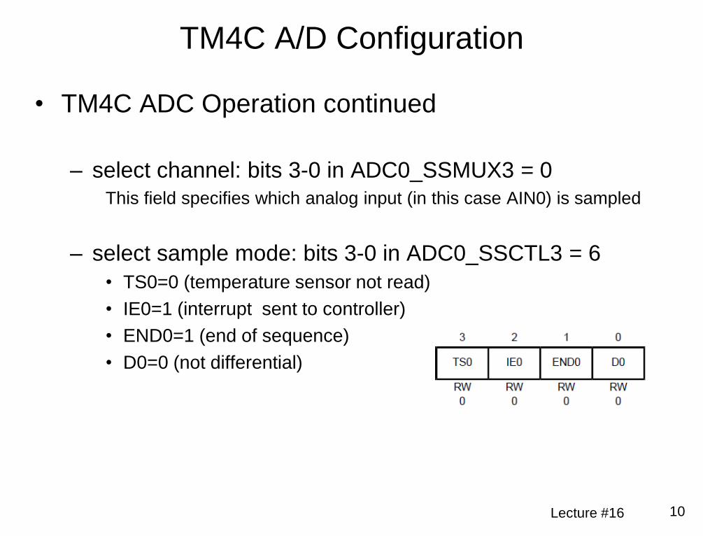
TM4C A/D Configuration
• TM4C ADC Operation continued
– select channel: bits 3-0 in ADC0_SSMUX3 = 0
This field specifies which analog input (in this case AIN0) is sampled
– select sample mode: bits 3-0 in ADC0_SSCTL3 = 6
• TS0=0 (temperature sensor not read)
• IE0=1 (interrupt sent to controller)
• END0=1 (end of sequence)
• D0=0 (not differential)
Lecture #16 10

TM4C A/D Initialization
• Initialization
– PLL (Phase Locked Loop) must be enabled for A/D Operation. Enable ADC clock: set bit 0 to 1 in SYSCTL_RCGCADC_R
– Set 125kHz ADC conversion speed: write 0x01 to ADC0_PC_R
– Set sequencer priority: 0,1,2,3 in ADC0_SSPRI_R
– Disable selected sequence 3: zero bit 3 of ADC0_ACTSS_R
– Set software start trigger event: zero bits 15-12 of ADC0_EMUX_R
– Set input source (0-11): write channel number in bits 3-0 of ADC0_SSMUX3_R
– Set sample control bits: write 0110 in bits 3-0 ADC0_SSCTL3_R to disable temp measurement, notify on sample complete, indicate single sample in sequence, and denote single-ended signal mode
– Disable interrupts: zero bit 3 of ADC0_IM_R
– Enable selected sequencer 3: set bit 3 of ADC0_ACTSS_R
Lecture #16 11

A/D on TM4C (see file ATD.s) ; Setup and run ATD sampling on ADC0 (AIN0 = PE3) Stores results in R5
; ADC Registers
RCGCADC EQU 0x400FE638 ; ADC clock register
;ADC0 base address EQU 0x40038000
ADC0_ACTSS EQU 0x40038000 ; Sample sequencer (ADC0 base address)
ADC0_RIS EQU 0x40038004 ; Interrupt status
ADC0_IM EQU 0x40038008 ; Interrupt select
ADC0_EMUX EQU 0x40038014 ; Trigger select
ADC0_PSSI EQU 0x40038028 ; Initiate sample
ADC0_SSMUX3 EQU 0x400380A0 ; Input channel select
ADC0_SSCTL3 EQU 0x400380A4 ; Sample sequence control
ADC0_SSFIFO3 EQU 0x400380A8 ; Channel 3 results
ADC0_PC EQU 0x40038FC4 ; Sample rate
; GPIO Registers
RCGCGPIO EQU 0x400FE608 ; GPIO clock register
;PORT E base address EQU 0x40024000
PORTE_DEN EQU 0x4002451C ; Digital Enable
PORTE_PCTL EQU 0x4002452C ; Alternate function select
PORTE_AFSEL EQU 0x40024420 ; Enable Alt functions
PORTE_AMSEL EQU 0x40024528 ; Enable analog
Lecture #16 12
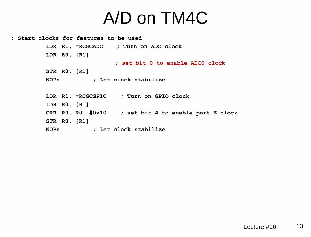
A/D on TM4C ; Start clocks for features to be used
LDR R1, =RCGCADC ; Turn on ADC clock
LDR R0, [R1]
; set bit 0 to enable ADC0 clock
STR R0, [R1]
NOPs ; Let clock stabilize
LDR R1, =RCGCGPIO ; Turn on GPIO clock
LDR R0, [R1]
ORR R0, R0, #0x10 ; set bit 4 to enable port E clock
STR R0, [R1]
NOPs ; Let clock stabilize
Lecture #16 13

A/D on TM4C ; Setup GPIO to make PE3 input for ADC0
; Enable alternate functions
LDR R1, =PORTE_AFSEL
LDR R0, [R1]
; set bit 3 to enable alt functions on PE3
STR R0, [R1]
; PCTL does not have to be configured since ADC0 is automatically selected when
port pin is set to analog.
; Disable digital on PE3
LDR R1, =PORTE_DEN
LDR R0, [R1]
; clear bit 3 to disable analog on PE3
STR R0, [R1]
; Eanable analog on PE3
LDR R1, =PORTE_AMSEL
LDR R0, [R1]
; set bit 3 to enable analog on PE3
STR R0, [R1]
Lecture #16 14
Setup A/D on TM4C ; Disable sequencer while ADC setup
LDR R1, =ADC0_ACTSS
LDR R0, [R1]
; clear bit 3 to disable seq'r 3
STR R0, [R1]
; Select trigger source
LDR R1, =ADC0_EMUX
LDR R0, [R1]
; clear bits 15:12 to select SOFTWARE
STR R0, [R1] ; trigger
; Select input channel
LDR R1, =ADC0_SSMUX3
LDR R0, [R1]
BIC R0, R0, #0x000F ; clear bits 3:0 to select AIN0
Lecture #16 15

Finish Setup, Enable Sequencer ; Config sample sequence
LDR R1, =ADC0_SSCTL3
LDR R0, [R1]
; set bits 2:1 (IE0, END0)
STR R0, [R1]
; Set sample rate
LDR R1, =ADC0_PC
LDR R0, [R1]
; set bits 3:0 to 1 for 125k sps
STR R0, [R1]
; Done with setup, enable sequencer
LDR R1, =ADC0_ACTSS
LDR R0, [R1]
; set bit 3 to enable seq'r 3
STR R0, [R1] ; sampling enabled but not initiated yet
Lecture #16 16

Sampling Subroutine ATD_Sample
PUSH {R0-R4}
; start sampling routine
LDR R3, =ADC0_RIS ; interrupt address
LDR R4, =ADC0_SSFIFO3 ; result address
LDR R2, =ADC0_PSSI ; sample sequence initiate address
; initiate sampling by enabling sequencer 3 in ADC0_PSSI
; wait 3 instructions
; check for sample complete (bit 3 of ADC0_RIS set)
; when complete, read results in ADC0_SSFIFO3 register
; reset the sample complete bit by setting bit IN3 of ADC0_ISC
; restore registers R0-R4 and return to caller
Lecture #16 17
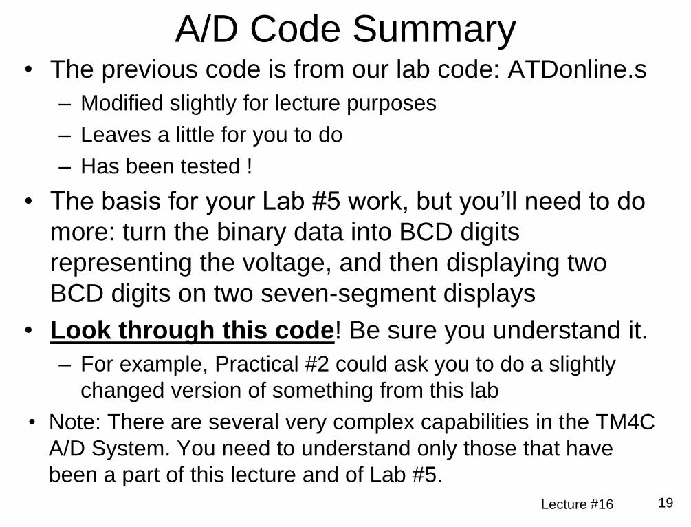
A/D Code Summary • The previous code is from our lab code: ATDonline.s
– Modified slightly for lecture purposes
– Leaves a little for you to do
– Has been tested !
• The basis for your Lab #5 work, but you’ll need to do
more: turn the binary data into BCD digits
representing the voltage, and then displaying two
BCD digits on two seven-segment displays
• Look through this code! Be sure you understand it.
– For example, Practical #2 could ask you to do a slightly
changed version of something from this lab
• Note: There are several very complex capabilities in the TM4C
A/D System. You need to understand only those that have
been a part of this lecture and of Lab #5.
Lecture #16 19
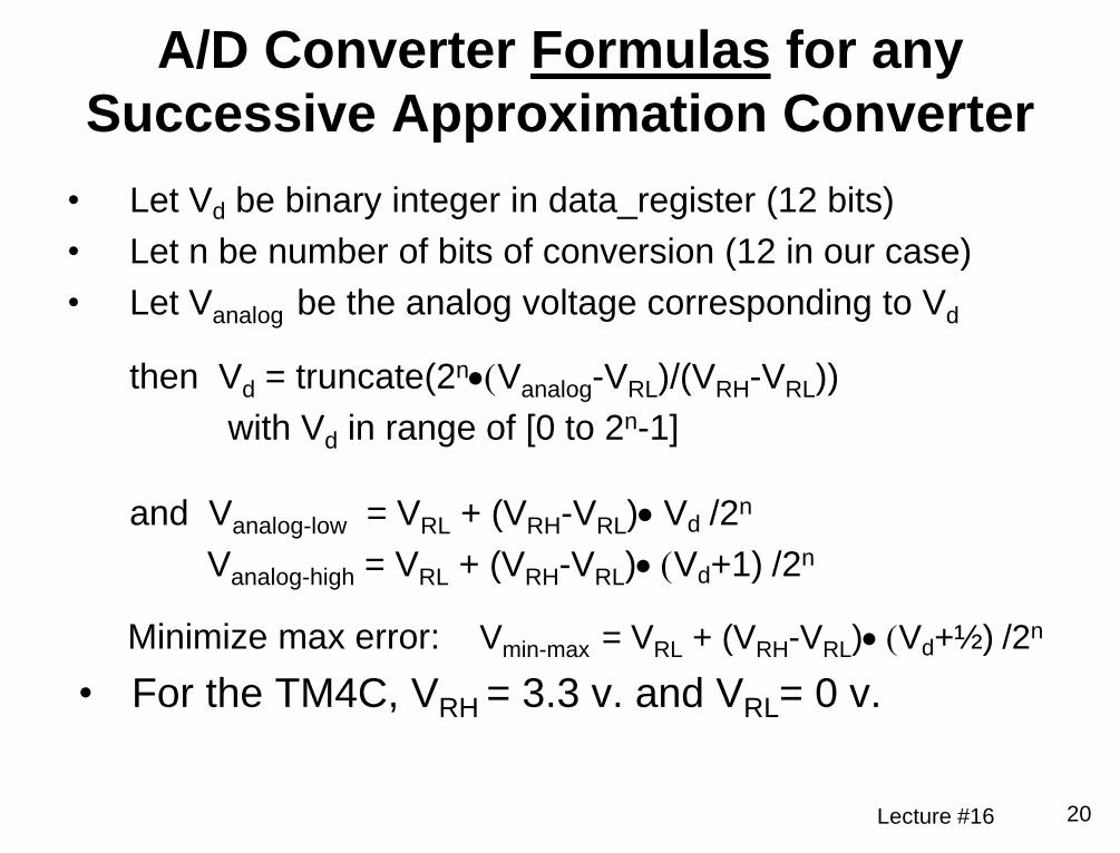
A/D Converter Formulas for any
Successive Approximation Converter
• Let Vd be binary integer in data_register (12 bits)
• Let n be number of bits of conversion (12 in our case)
• Let Vanalog be the analog voltage corresponding to Vd
then Vd = truncate(2nVanalog-VRL)/(VRH-VRL))
with Vd in range of [0 to 2n-1]
and Vanalog-low = VRL + (VRH-VRL)Vd/2n
Vanalog-high = VRL + (VRH-VRL)Vd+1)/2n
Minimize max error: Vmin-max = VRL + (VRH-VRL)Vd+½)/2n
• For the TM4C, VRH = 3.3 v. and VRL= 0 v.
Lecture #16 20

A/D Result Example
• 12-bit A/D converter. VRL = 0 v. and VRH = 3.3 v.
• We have requested a conversion on AIN0, and find
the following register value: y = 0xC94;
What voltage does this represent?
• Solution: Vanalog-low = (3.3)0xC94/212 v.
= 3.33220/4096
= 2.594238 v.
Vanalog-hi = 3.33221/4096
= 2.595044 v.
Vmin-max = 3.33220.5/4096
= 2.594641 v.
VRANGE = (2.595044 to 2.594238) v.
Note: VRES-12 bit = 3.3/4096 = .000806 v. = 806 µv.
Lecture #16 21
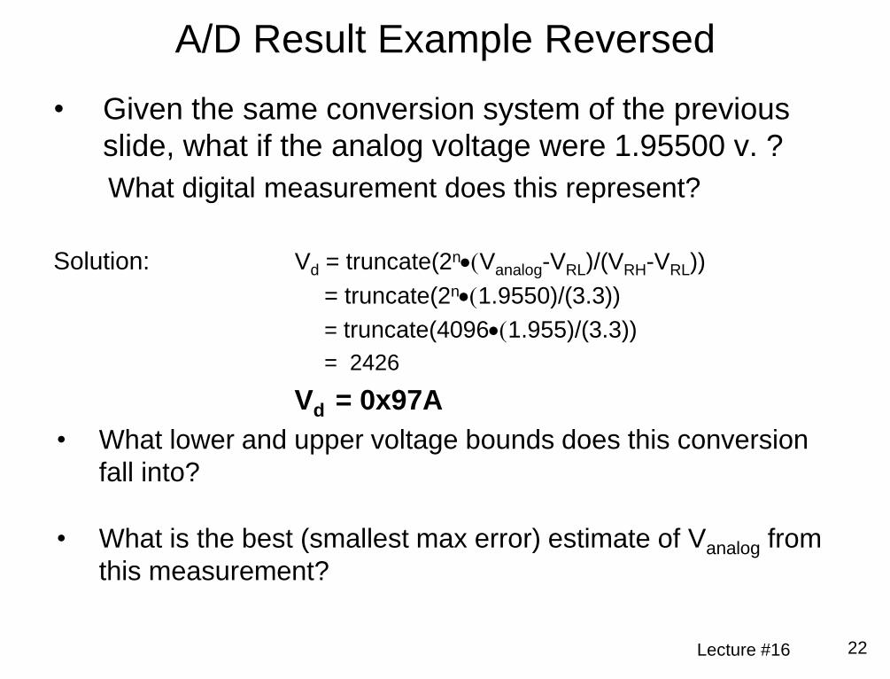
• Given the same conversion system of the previous
slide, what if the analog voltage were 1.95500 v. ?
What digital measurement does this represent?
Solution: Vd = truncate(2nVanalog-VRL)/(VRH-VRL))
= truncate(2n1.9550)/(3.3))
= truncate(40961.955)/(3.3))
= 2426
Vd = 0x97A
• What lower and upper voltage bounds does this conversion
fall into?
• What is the best (smallest max error) estimate of Vanalog from
this measurement?
A/D Result Example Reversed
Lecture #16 22

Lecture #16+ 27
Calculations Needed • The A/D Converter gives a 12 bit result Vd, 0x000 to
0xFFF, corresponding to 0 v. to 3.3- v. (0x1000
would correspond to exactly 3.3 v.)
• To get the numerical value for the voltage Vn
corresponding to the digital reading you could use:
Vn/3.3 = Vd/4096 or Vn = Vd(3.3/4096)
• But this would give us only the integer component
part of the answer. Is there any simple way to get the
answer to include “p” digits of precision? What is the
appropriate value of “p” for our D/A Converter?
• … Think about it. Choosing “p” is easy; there’s a
simple method to get Vn; it’s YOUR job to find it.
Lecture #16+ 28
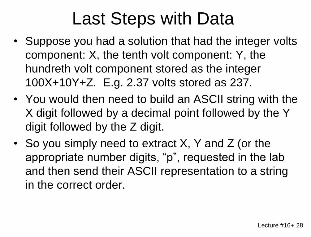
Last Steps with Data • Suppose you had a solution that had the integer volts
component: X, the tenth volt component: Y, the
hundreth volt component stored as the integer
100X+10Y+Z. E.g. 2.37 volts stored as 237.
• You would then need to build an ASCII string with the
X digit followed by a decimal point followed by the Y
digit followed by the Z digit.
• So you simply need to extract X, Y and Z (or the
appropriate number digits, “p”, requested in the lab
and then send their ASCII representation to a string
in the correct order.

• Successive Approximation: Good compromise for A/D
Conversion speed and accuracy
• Method for A/D conversion and with TM4C and
sending to a string has been explained and will be
used in Lab #5
• The TM4C capability is extensive and exhaustive
(and exhausting)
• Next Lecture: SysTick Real Time Clock-
– Section 11.4 in text (same as our SysTick subsystem)
Summary
Lecture #16 30