EE2356 LAB Manuel 2014-15chettinadtech.ac.in/storage/15-07-03/15-07-03-14-14-36...VELALAR COLLEGE OF...
110
VELALAR COLLEGE OF ENGINEERING AND TECHNOLOGY DEPARTMENT OF EEE EE2356-MICROPROCESSOR AND MICROCONTROLLER LAB MANUEL Prepared by C.GOKUL, AP/EEE, VCET www.Vidyarthiplus.com www.Vidyarthiplus.com
Transcript of EE2356 LAB Manuel 2014-15chettinadtech.ac.in/storage/15-07-03/15-07-03-14-14-36...VELALAR COLLEGE OF...

VELALAR COLLEGE OF ENGINEERING AND TECHNOLOGY
DEPARTMENT OF EEE
EE2356-MICROPROCESSOR AND MICROCONTROLLER LAB MANUEL
Prepared by
C.GOKUL,
AP/EEE,
VCET
www.Vidyarthiplus.com
www.Vidyarthiplus.com

Ex. No:
Date :
STUDY OF 8085 MICROPROCESSOR.
AIM:
To study the architecture of 8085 Microprocessor.
MICROPROCESSOR ARCHITECTURE:
The Microprocessor is a programmable digital device designable with Register flip-flops
and timing elements. Data manipulation and communication is determined by the logic design
of the Microprocessor is called Architecture.
MICROPROCESSOR UNIT:
The Microprocessor unit is designed as a group of device input of the function with
necessary set of control signals.
8085 MICROPROCESSOR:
The 8085 Microprocessor is an 8 bit general purpose Microprocessor, capable of
addressing 64 KB of memory. The chip has 40 pins and required as +5 V. It has a Single
processor supply and operates with 3 Hz single phase clock.
8085 BUS ORGANIZATION:
The 8085 Microprocessor perform different operation using three sorts of
communication lines called Buses.
ADDRESS BUS:
The address bus is a group of 16 lines, generally identify as A0-A15. The address bus is in
uni-direction. The bits following one direction from the Microprocessor unit to peripheral
devices (or) memory devices are called unidirectional
www.Vidyarthiplus.com
www.Vidyarthiplus.com

DATA BUS:
The data bus is a group of 8 lines used to flow. These lines are bidirectional in which the
data flows in both the direction between the Microprocessor unit and the memory peripheral
devices. The Microprocessor unit uses this bus to transfer the binary information.
CONTROL BUS:
The control bus is compressed of various lines with carry synchronization symbols. The
Microprocessor unit uses such lines to provide timing signals.
ACCUMULATOR:
This is an 8 bit register that is a part of ALU; this register is used to store 8 bit data to
perform arithmetic and logical operation. This accumulator is identified as register A.
FLAGS:
The ALU includes BPF’s that are set or reset according to the result of an operation. The
Microprocessor unit uses this to test the data conditions. The 8085 flags indicate 5 different
types of results.
SIGN FLAG:
After the execution of an arithmetic and logical operation of a bit or if the result is ‘1’,
the flag is used with signed numbers in the given byte.
ZERO FLAG:
The zero flag is set when the ALU operation byte results is zero and reset if the results is
not zero. The flag is modified by the result in accumulator.
PROGRAM STATUS WORD:
This is nothing but the combination of an accumulator and the flag registers. The
accumulator forms the higher bytes and the flag registers forms the lower bytes.
RESULT:
www.Vidyarthiplus.com
www.Vidyarthiplus.com

Ex. No : 1
Date :
Arithmetic operations using 8085
(8 bit addition,8 bit subtraction,8 bit multiplication,8 bit division)
AIM:
To write an assembly language program for adding, subtracting, multiplying & division
two 8 bit numbers using 8085 microprocessor kit.
APPARATUS REQUIRED:
S.No Apparatus Required Quantity
1. 8085 Microprocessor kit 1
2. Power supply -
ALGORITHM FOR 8-BIT ADDITION:
1. Start the program.
2. Load the first data in the accumulator.
3. Move the content of A to B register.
4. Load the second data in the accumulator.
5. Initialize the carry with zero.
6. Add the content of B register to the accumulator.
7. If the carry is “0” then store the result in address which is specified.
8. If the carry is “1” then increment the C register and store the result.
9. Stop the program
www.Vidyarthiplus.com
www.Vidyarthiplus.com

FLOW CHART FOR 8 BIT ADDITION:
DATA CHECK MAP FOR 8 BIT ADDITION:
MEMORY ADDRESS
DATA 1
(WITHOUT
CARRY)
DATA 2
(WITH
CARRY)
INPUT 8200H
8201H
05
04
FF
03
OUTPUT 8300H(SUM)
8301H(CARRY)
09
00
02
01
MANUAL CALCULATION:
www.Vidyarthiplus.com
www.Vidyarthiplus.com

PROGRAM FOR 8-BIT ADDITION:
MEMORY LABEL MNEMONICS OPCODE COMMENTS
8500 START LDA 8200H
8503 MOV B,A
8504 LDA 8201H
8507 MVI C,00
8509 ADD B
850A JNC LOOP1
850D INR C
850E LOOP1 STA 8300H
8511 MOV A,C
8512 STA 8301H
8515 STOP HLT
FLOW CHART FOR 8 BIT SUBTRACTION:
ALGORITHM FOR 8 BIT SUBTRACTION:
1. Start the program.
2. Load the first data in the accumulator.
3. Move the content of A to B register.
www.Vidyarthiplus.com
www.Vidyarthiplus.com

4. Load the second data in the accumulator.
5. Subtract the content of B register from the accumulator.
6. If the borrow is “0” then go to step 7.
7. Store the result.
8. Stop the program.
DATA CHECK MAP FOR 8 BIT SUBTRACTION:
MEMORY
ADDRESS
DATA 1
(WITHOUT BORROW)
DATA 2
(WITH BORROW)
INPUT 8200H
8201H
OUTPUT 8300H
8301H
MANUAL CALCULATION:
PROGRAM FOR 8 BIT SUBTRACTION:
MEMORY LABEL MNEMONICS OPCODE COMMENTS
8500 START LDA 8200H
8503 MOV B,A
8504 LDA 8201H
8507 MVI C,00
8509 SUB B
850A JNC LOOP1
850D INR C
850E LOOP1 STA 8300H
8511 MOV A,C
8512 STA 8301H
8515 STOP HLT
www.Vidyarthiplus.com
www.Vidyarthiplus.com

FLOW CHART FOR 8 BIT MULTIPLICATION:
ALGORITHM FOR 8-BIT MULTIPLICATION:
Start the program.
Load the first data into the accumulator.
Move the content of accumulator to the B register.
Load the second data into the accumulator.
Move the content of accumulator to the C register.
Decrement the content of B register by one.
Add the C register content with accumulator.
Decrement the content of B register & then repeat the steps 7 & 8.
Else store the result in the memory location mentioned.
Stop the program.
www.Vidyarthiplus.com
www.Vidyarthiplus.com

DATA CHECK MAP FOR 8 BIT MULTIPLICATION:
MEMORY
LOCATION
DATA1
DATA 2
INPUT
8200H
8201H
OUTPUT
8300H(Reminder)
8301H(Quotient)
MANUAL CALCULATION:
PROGRAM FOR 8 BIT MULTIPLICATION:
MEMORY LABEL MNEMONICS OPCODE COMMENTS
8500 START LDA 8200H
8503 MOV D,A
8504 LDA 8201H
8507 MOV B,A
8508 DCR D
8509 MVI C,00
850B L2 ADD B
850C JNC 8510 (L1)
850F INR C
8510 L1 DCR D
8511 JNZ 850B (L2)
8514 STA 8300
8517 MOV A,C
8518 STA 8301
851B HLT
www.Vidyarthiplus.com
www.Vidyarthiplus.com

FLOW CHART FOR 8 BIT DIVISION:
ALGORITHM FOR 8 BIT DIVISION:
Start the program.
Load the first data in the accumulator.
Move the content from memory address to A register and increment the HL pair.
Move the content from memory address to B register & initialize the C register.
Compare the 8 bit instructions in A and B registers. Subtract B register from
accumulator & increment the value in C register.
Increment the HL pair and move the content in accumulator to memory.
Stop the program.
www.Vidyarthiplus.com
www.Vidyarthiplus.com

DATA CHECK MAP FOR 8 BIT DIVISION:
MEMORY
LOCATION
DATA1
DATA 2
INPUT
8200H
8201H
OUTPUT
8301(Reminder)
8302(Quotient)
MANUAL CALCULATION:
PROGRAM FOR 8 BIT DIVISION:
MEMORY LABEL MNEMONICS OPCODE COMMENTS
8500 START LDA 8200
8503 MOV D,A
8504 LDA 9201
8507 MVI C,00
8509 L1 SUB D
850A INR C
850B CMP D
850C JNC 8509(L1)
850F STA 8300
8512 MOV A,C
8513 STA 9301
8516 HLT
RESULT:
www.Vidyarthiplus.com
www.Vidyarthiplus.com
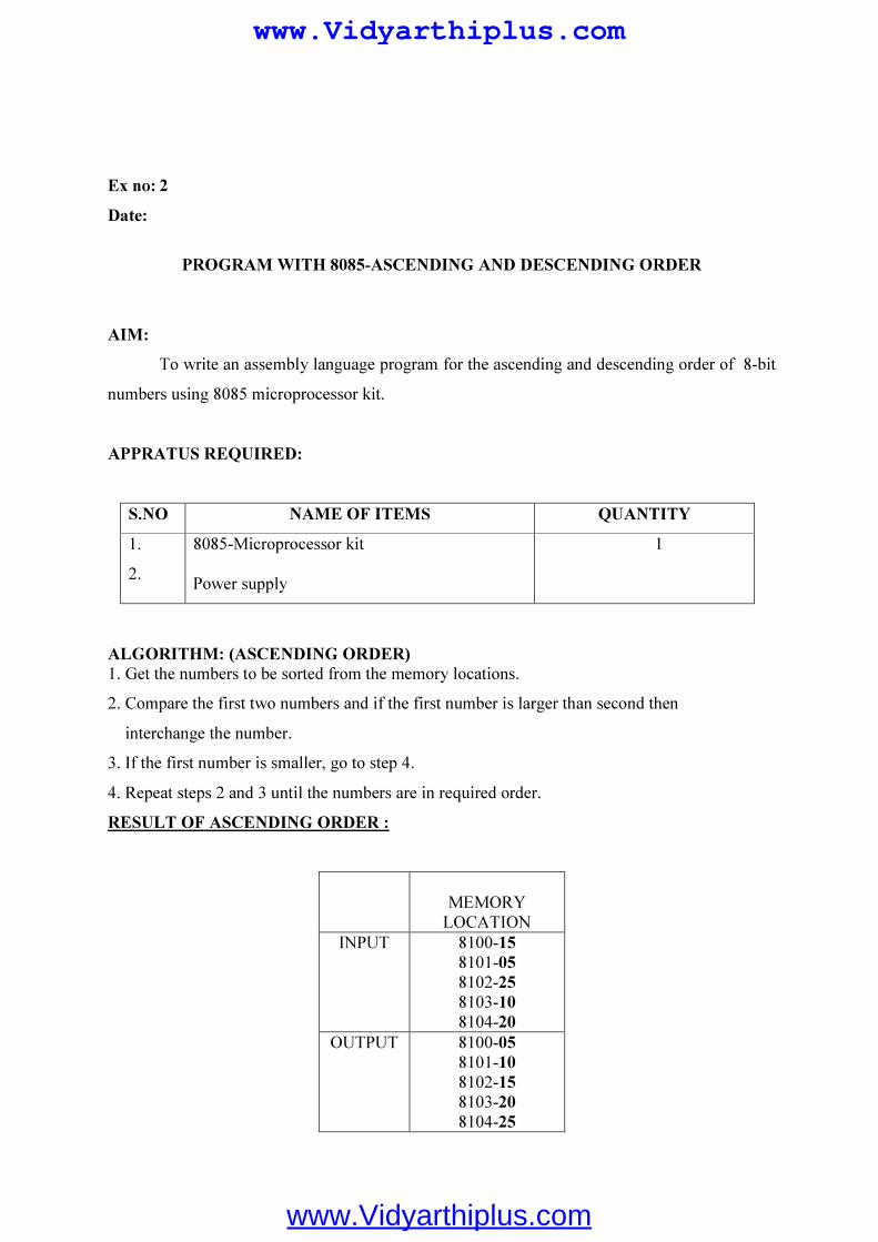
Ex no: 2
Date:
PROGRAM WITH 8085-ASCENDING AND DESCENDING ORDER
AIM:
To write an assembly language program for the ascending and descending order of 8-bit
numbers using 8085 microprocessor kit.
APPRATUS REQUIRED:
S.NO NAME OF ITEMS QUANTITY
1.
2.
8085-Microprocessor kit Power supply
1
ALGORITHM: (ASCENDING ORDER)
1. Get the numbers to be sorted from the memory locations.
2. Compare the first two numbers and if the first number is larger than second then
interchange the number.
3. If the first number is smaller, go to step 4.
4. Repeat steps 2 and 3 until the numbers are in required order.
RESULT OF ASCENDING ORDER :
MEMORY LOCATION
INPUT
8100-15 8101-05 8102-25 8103-10 8104-20
OUTPUT
8100-05 8101-10 8102-15 8103-20 8104-25
www.Vidyarthiplus.com
www.Vidyarthiplus.com

MODEL CALCULATION
PROGRAM: (ASCENDING ORDER)
ADD
RESS OPCODE LABEL MNEMONICS COMMENTS
8000 MVI B,04 Comparison of N-1 Numbers(5Nos)
8002 LOOP 3 LXI H,8100
8005 MVI C,04
8007 LOOP2 MOV A,M
8008 INX H
8009 CMP M
800A JC LOOP1(8012)
800D MOV D,M
800E MOV M,A
800F DCX H
8010 MOV M,D
8011 INX H
8012 LOOP1 DCR C
8013 JNZ LOOP2(8007)
8016 DCR B
8017 JZ LOOP3(8002)
801A HLT
ALGORITHM :( DESCENDING ORDER)
1. Get the numbers to be sorted from the memory locations. 2. Compare the first two numbers and if the first number is SMALLER than second then interchange the number. 3. If the first number is LARGER, go to step 4. 4. Repeat steps 2 and 3 until the numbers are in required order.
RESULT OF DESCENDING ORDER :
MEMORY LOCATION
INPUT
8100-15 8101-05 8102-25 8103-10 8104-20
OUTPUT
8100-25 8101-20 8102-15 8103-10 8104-05
www.Vidyarthiplus.com
www.Vidyarthiplus.com

MODEL CALCULATION
PROGRAM: (DESCENDING ORDER)
ADDRESS OPCODE LABEL MNEMONICS COMMENTS
8000 MVI B,04 Comparison of N-1 Numbers(5Nos)
8002 LOOP3 LXI H,8100
8005 MVI C,04
8007 LOOP2 MOV A,M
8008 INX H
8009 CMP M
800A JNC LOOP1(8012)
800D MOV D,M
800E MOV M,A
800F DCX H
8010 MOV M,D
8011 INX H
8012 LOOP1 DCR C
8013 JNZ LOOP2(8007)
8016 DCR B
8017 JZ LOOP3(8002)
801A HLT
RESULT:
www.Vidyarthiplus.com
www.Vidyarthiplus.com

Ex no:3
Date:
PROGRAM WITH 8085- MINIMUM AND MAXIMUM NUMBER
IN A GROUP OF DATA (Smallest & Largest number )
AIM:
To write an assembly language program to search the minimum and maximum number
in a group of data using 8085 microprocessor kit.
APPRATUS REQUIRED:
S.NO NAME OF ITEMS QUANTITY
1.
2.
8085-Microprocessor kit Power supply
1
ALGORITHM :( SEARCH THE MINIMUM NUMBER)
1. Place all the elements of an array in the consecutive memory locations.
2. Fetch the first element from the memory location and load it in the accumulator.
3. Initialize a counter (register) with the total number of elements in an array.
4. Decrement the counter by 1.
5. Increment the memory pointer to point to the next element.
6. Compare the accumulator content with the memory content (next element).
7. If the accumulator content is smaller, then move the memory content (largest
element) to the accumulator. Else continue.
8. Decrement the counter by 1.
9. Repeat steps 5 to 8 until the counter reaches zero
10. Store the result (accumulator content) in the specified memory location.
RESULT OF SEARCH THE MINIMUM NUMBER:
MEMORY LOCATION
DATA1
DATA 2
INPUT
8100 8101 8102 8103 8104
25 10 05 30 15
2B 5F 4D 3C 1A
OUTPUT 8200 05 1A
www.Vidyarthiplus.com
www.Vidyarthiplus.com

MODEL CALCULATION:
PROGRAM: (SEARCH THE MINIMUM NUMBER)-SMALLEST NUMBER
ADDRESS OPCODE LABEL MNEMONICS COMMENTS
8000 LXI H,8100H
8003 MOV B,05 Comparison of 5 Nos
8005 DEC B
8006 MOV A,M
8007 LOOP1 INX H
8008 CMP M
8009 JC AHEAD(800D)
800C MOV A,M
800D AHEAD DCR B
800E JNZ LOOP1(8007)
8011 STA 8200H
8014 STOP HLT
ALGORITHM :( SEARCH THE MAXIMUM NUMBER)
1. Place all the elements of an array in the consecutive memory locations. 2. Fetch the first element from the memory location and load it in the accumulator. 3. Initialize a counter (register) with the total number of elements in an array. 4. Decrement the counter by 1. 5. Increment the memory pointer to point to the next element. 6. Compare the accumulator content with the memory content (next element). 7. If the accumulator content is smaller, then move the memory content (largest element) to the accumulator. Else continue. 8. Decrement the counter by 1. 9. Repeat steps 5 to 8 until the counter reaches zero 10.Store the result (accumulator content) in the specified memory location. RESULT OF SEARCH THE MAXIMUM NUMBER(Largest Number)
MEMORY LOCATION
DATA1
DATA 2
INPUT
8100 8101 8102 8103 8104
25 10 05 30 15
2B 5F 4D 3C 1A
OUTPUT 8200 30 5F
www.Vidyarthiplus.com
www.Vidyarthiplus.com

MODEL CALCULATION
PROGRAM: (SEARCH THE MAXIMUM NUMBER)-Largest number
ADDRESS OPCODE LABEL MNEMONICS COMMENTS
8000 LXI H,8100H
8003 MOV B,05 Comparison of 5 Nos
8005 DEC B
8006 MOV A,M
8007 LOOP1 INX H
8008 CMP M
8009 JNC AHEAD(800D)
800C MOV A,M
800D AHEAD DCR B
800E JNZ LOOP1(8007)
8011 STA 8200H
8014 STOP HLT
RESULT:
www.Vidyarthiplus.com
www.Vidyarthiplus.com

EX.NO:4
DATE: STUDY OF ROTATE INSTRUCTION
AIM:
To rotate and execute an assembly language program to perform instruction.
APPARATUS REQUIRED:
1. 8085 kit
2. Power chord
ALGORITHM:
Program using RLC:
1. Start the program
2. Load the input and add them
3. Then the input values are rotated using RLC
4. Stop the program
Program using RRC:
1. Start the program
2. Load the input and add them
3. Now the input is rotated using RRC
4. Stop the program
Program using RAL:
1. Start the program
2. Load the input and add them
3. Then the input is rotated using rotate accumulator left through carry
4. Stop the program
Program using RAR:
1. Start the program
2. Load the input data and add them
3. Then the input is rotated using rotate the accumulator right through carry
4. Stop the program
PROGRAM USING RLC:
Memory
address
Mnemonics Opcode Comments
8100 LXI H,8500
8103 MOV A,B
8104 INX H
8105 ADD M
www.Vidyarthiplus.com
www.Vidyarthiplus.com

8106 RLC
8107 STA 8600
810A HLT
Program using RRC:
Memory
address
Mnemonics Opcode Comments
8100 LXI H,8500
8103 MOV A,M
8104 INX H
8105 ADD M
8106 RRC
8107 STA 8600
810A HLT
Program using RAL:
Memory
Address
Mnemonics Opcode Comments
8100 LXI H,8500
8103 MOV A,M
8104 INX H
8105 ADD M
8106 RAL
8107 STA 8600
810A HLT
PROGRAM USING RAR:
Memory
Address
Mnemonics Opcode Comments
8100 LXI H,8500
8103 MOV A,M
8104 INX H
8105 ADD M
8106 RAR
8107 STA 8600
810A HLT
www.Vidyarthiplus.com
www.Vidyarthiplus.com

RLC:
INPUT OUTPUT
Memory
address
Data Memory
address
data
RRC:
INPUT OUTPUT
Memory
address
data Memory
address
data
RAL:
INPUT OUTPUT
Memory
address
data Memory
address
data
RAR:
INPUT OUTPUT
Memory
address
data Memory
address
data
RESULT:
Prepared by C.GOKUL,AP/EEE
www.Vidyarthiplus.com
www.Vidyarthiplus.com

EX.No.5 Hex / ASCII / BCD code conversions
DATE:
AIM:
To write an assembly language program to convert i. ASCII to Hexa ii. Hexa to ASCII iii.BCD to Hexa iv. Hexa to BCD
A) ASCII to Hexa Decimal Conversion:
Memory address
Label Mnemonics Opcode Comments
8100 LDA 8200
8103 SUI 30
8105 CPI 0A
8107 JC LOOP
810A SUI 07
810C LOOP STA 8300
810F HLT
INPUT OUTPUT
Memory address Data Memory address Data
8200 41 8300 0A
www.Vidyarthiplus.com
www.Vidyarthiplus.com

B) Hexa Decimal TO ASCII Conversion:
Memory address
Mnemonics Opcode Comments
8100 LDA 8200
8103 MOV B,A
8104 ANI 0F
8107 CALL LOOP
8108 STA 8201
8109 MOV A,B
810C ANI F0
810D RLC
810E RLC
810F RLC
8112 RLC
8113 CALL LOOP
8115 STA 8202
8117 HLT
LOOP: CPI 0A
JC LOOP2
ADI 07
LOOP2: ADI 30
RET
www.Vidyarthiplus.com
www.Vidyarthiplus.com

INPUT: 8200-E4(hexa value)
OUTPUT:8201-34(ASCII code for 4)
8202-45(ASCII code for E)
C) BCD to HEX conversion:
Memory address
Mnemonics Opcode Comments
8100 LXI H,8200
MOV A,M
ADD A
MOV B,A
ADD A
ADD A
ADD B
INX H
ADD M
INX H
MOV M,A
HLT
INPUT: 8200-02(MSD) 8201-09(LSD)
OUTPUT:8202-1DH
www.Vidyarthiplus.com
www.Vidyarthiplus.com
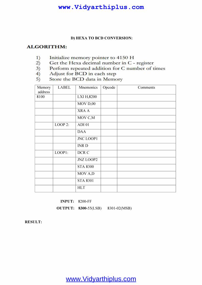
D) HEXA TO BCD CONVERSION:
Memory address
LABEL Mnemonics Opcode Comments
8100 LXI H,8200
MOV D,00
XRA A
MOV C,M
LOOP 2: ADI 01
DAA
JNC LOOP1
INR D
LOOP1: DCR C
JNZ LOOP2
STA 8300
MOV A,D
STA 8301
HLT
INPUT: 8200-FF
OUTPUT: 8300-55(LSB) 8301-02(MSB)
RESULT:
www.Vidyarthiplus.com
www.Vidyarthiplus.com

8 CHANNEL ADC INTERFACE with 8085
EX NO: 6
DATE:
AIM:
To study the operation of the 8 channel selection and analog to digital converter details.
APPARATUS REQUIRED:
1. 8 channel ADC trainer kit 1
2. CRO 1
3. Patch chords as Req
PROCEDURE:
1. Connect the 26pin FRC to kit and insert power cable.
2. Switch ON the trainer kit.
3. Check all 8 channel input’s and measure it.
4. Enter the given ADC program into the MP/MC kit.
5. If the channel selection is pb2 to pb0 [0 0 0] the CH0 will connect to the MUX output
line. Now we get to CH0 corresponding digital value see in LCD. Similarly CH0 to
CH7are connected to the MUX output line based on the status of the channel selection
for pb2to pb0.
6. Execute the program.
7. Now check stepno.3
8. Repeat the steps 3 and 5. Observe the multiplexer output and ADC output
www.Vidyarthiplus.com
www.Vidyarthiplus.com
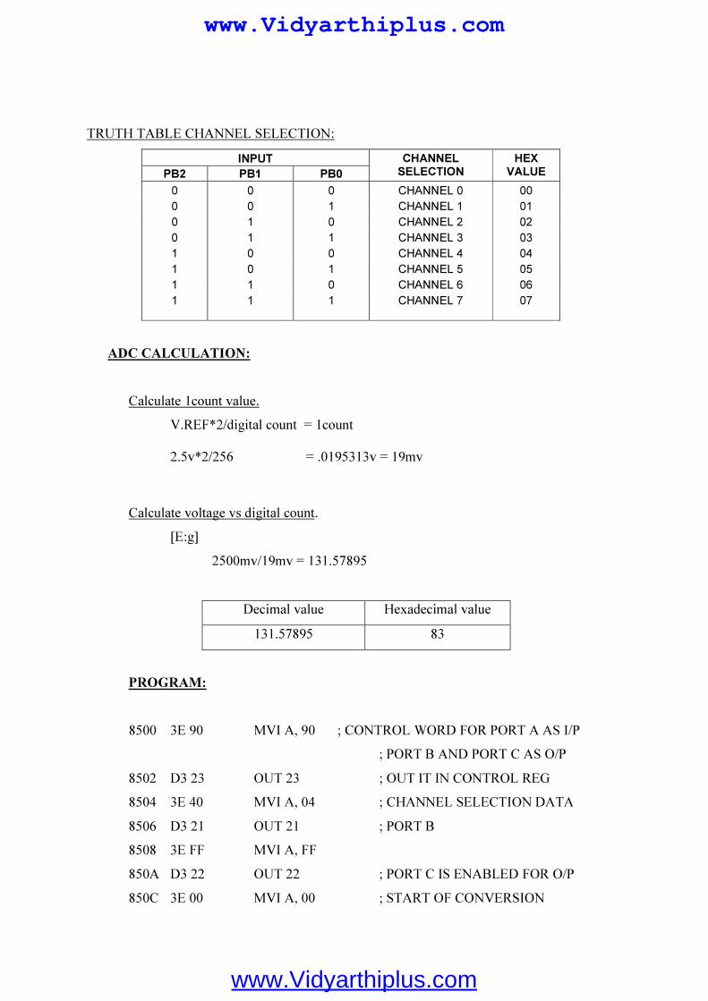
TRUTH TABLE CHANNEL SELECTION:
INPUT CHANNEL
SELECTION
HEX
VALUE PB2 PB1 PB0
0 0 0 CHANNEL 0 00
0 0 1 CHANNEL 1 01
0 1 0 CHANNEL 2 02
0 1 1 CHANNEL 3 03
1 0 0 CHANNEL 4 04
1 0 1 CHANNEL 5 05
1 1 0 CHANNEL 6 06
1 1 1 CHANNEL 7 07
ADC CALCULATION:
Calculate 1count value.
V.REF*2/digital count = 1count
2.5v*2/256 = .0195313v = 19mv
Calculate voltage vs digital count.
[E:g]
2500mv/19mv = 131.57895
Decimal value Hexadecimal value
131.57895 83
PROGRAM:
8500 3E 90 MVI A, 90 ; CONTROL WORD FOR PORT A AS I/P
; PORT B AND PORT C AS O/P
8502 D3 23 OUT 23 ; OUT IT IN CONTROL REG
8504 3E 40 MVI A, 04 ; CHANNEL SELECTION DATA
8506 D3 21 OUT 21 ; PORT B
8508 3E FF MVI A, FF
850A D3 22 OUT 22 ; PORT C IS ENABLED FOR O/P
850C 3E 00 MVI A, 00 ; START OF CONVERSION
www.Vidyarthiplus.com
www.Vidyarthiplus.com
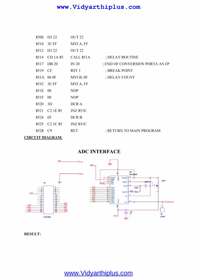
850E D3 22 OUT 22
8510 3E FF MVI A, FF
8512 D3 22 OUT 22
8514 CD 1A 85 CALL 851A ; DELAY ROUTINE
8517 DB 20 IN 20 ; END OF CONVERSION PORTA AS I/P
8519 CF RST 1 ; BREAK POINT
851A 06 0F MVI B, 0F ; DELAY COUNT
851C 3E FF MVI A, FF
851E 00 NOP
851F 00 NOP
8520 3D DCR A
8521 C2 1E 85 JNZ 851E
8524 05 DCR B
8525 C2 1C 85 JNZ 851C
8528 C9 RET ; RETURN TO MAIN PROGRAM
CIRCUIT DIAGRAM:
ADC INTERFACE
RESULT:
www.Vidyarthiplus.com
www.Vidyarthiplus.com

Ex.No : 7
Date :
INTERFACING 8279 WITH 8085 MICROPROCESSOR
(KEYBOARD AND DISPLAY INTERFACE)
AIM:
To write an assembly language Program to interface keyboard.
APPARATUS REQUIRED:
S.No APPARATUS QUANTITY
1. 8085 Microprocessor kit 1
2. Power supply 1
3. Interface kit 1
KEYBOARD PROGRAME FOR 8085:
9000 3E 12 MVI A, 12
9002 32 01 60 STA 6001
9005 3E 3E MVI A, 3E
9007 32 01 60 STA 6001
900A 3E A0 MVI A, A0
900C 32 01 61 STA 6001
900F 06 08 MVI B, 08
9011 3E 00 loop: MVI A, 00
9013 32 00 60 STA 6000
9016 05 DCR B
9017 C2 11 90 JNZ loop
901A 3A 01 60 L1:LDA 6001
901D E6 07 ANI 07
www.Vidyarthiplus.com
www.Vidyarthiplus.com

901F CA 1A 90 JZ L1
9022 3A 00 60 LDA 6000
9025 E6 3F ANI 3F
9027 CF RST 1
DISPLAY PROGRAME FOR 8085:
8500 3E 12 MVI A,12 ; control word to define 8279
; In 8 bit 8 character display
8502 32 01 61 STA 6001 ; 8279 control port
8505 3E 3E MVI A,3E ; for frequency division into 8279
8507 32 01 60 STA 6001 ; into 8279 control reg.
850A 3E A0 MVI A,A0 ; display/write inhibit
850C 32 01 60 STA 6001 ; into 8279
850F 06 08 MVI B,08
8511 3E 00 MVI A,00 ;clear the display
8513 32 00 60 L1: STA 6000
8516 05 DCR B
8517 C2 13 85 JNZ L1
851A 0E 06 MVI C,06
851C 21 00 90 LXI H,9000 ;Input code starting address
851F 7E L2: MOV A,M
8520 32 00 60 STA 6000
8523 23 INX H
8524 0D DCR C
8525 C2 1F 85 JNZ L2
8523 CF RST 1
INPUT CODE ADDRESS:
1ST
Digit 9000
2ND
Digit 9001
3RD
Digit 9002
www.Vidyarthiplus.com
www.Vidyarthiplus.com
4TH
Digit 9003
5TH
Digit 9004
6TH
Digit 9005
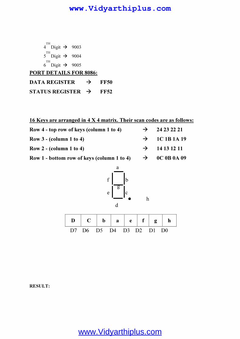
PORT DETAILS FOR 8086:
DATA REGISTER FF50
STATUS REGISTER FF52
16 Keys are arranged in 4 X 4 matrix. Their scan codes are as follows:
Row 4 - top row of keys (column 1 to 4) 24 23 22 21
Row 3 - (column 1 to 4) 1C 1B 1A 19
Row 2 - (column 1 to 4) 14 13 12 11
Row 1 - bottom row of keys (column 1 to 4) 0C 0B 0A 09
a
f b
g
e c
h
d
D7 D6 D5 D4 D3 D2 D1 D0
RESULT:
D C b a e f g h
www.Vidyarthiplus.com
www.Vidyarthiplus.com

Ex.No : 8
Date :
INTERFACING 8253/8254 WITH 8085
Timer/counter
AIM:
To interface 8253/8254 with 8085 to perform Square wave generation,
APPARATUS REQUIRED:
S.No APPARATUS QUANTITY
1 Microprocessor kit 1
2 Interface kit 1
Working Description:
Enter the program in to the trainer kit. Then give the clock input to the selected Counter.
Now run the program and view the output of the selected counter. The user can give his input to
the CLK0 or CLK1 or CLK2 from the PCLK through a wire connector. They can view the
output pulses in out 0, out 1, out 2 pins.
The I/O address for 8085:
Counter 0 - 4000
Counter 1 - 4001
Counter 2 - 4002
Control reg - 4003
Steps:
Enter the program into the kit.
Connect the PCLK and CLK2 through a wire connecter.
Now execute the program.
Now see the output waveform on the OUT2.
www.Vidyarthiplus.com
www.Vidyarthiplus.com

ASYNCHRONOUS MODE:
www.Vidyarthiplus.com
www.Vidyarthiplus.com

PROGRAM FOR 8085
PROGRAM 1:
9000: 3E 37 MVI A, 37 ; cntrl word for 8253.counter 0 is selected
9002: 32 03 40 STA 4003 ; cntrl reg
9005: 3E F7 MVI A, F7 ; LSB of the frequency divider
9007: 32 00 40 STA 4000 ; out it in counter 0
900A: 3E 00 MVI A, 00 ; MSB of the frequency divide
900C: 32 00 40 STA 4000 ; out it in counter 0
900F: CF RST 1 ; end
Note: A change in the value of MSB and LSB causes the change in frequency of Counter 0 PROGRAM 2:
9000: 3E 77 MVI A, 77 ; cntrl word for 8253.counter 1 is selected
9002: 32 03 40 STA 4003 ; cntrl reg
9005: 3E F7 MVI A, F7 ; LSB of the frequency divider
9007: 32 01 40 STA 4001 ; out it in counter 1
900A: 3E 00 MVI A, 00 ; MSB of the frequency divider
900C: 32 01 40 STA 4001 ; out it in counter 1
900F: CF RST 1 ; end
Note: A change in the value of MSB and LSB causes the change in frequency of Counter 1
PROGRAM 3:
9000: 3E B7 MVI A, B7 ; cntrl word for 8253.counter 2 is selected
9002: 32 03 40 STA 4003 ; cntrl reg
9005: 3E F7 MVI A, F7 ; LSB of the frequency divider
9007: 32 02 40 STA 4002 ; out it in counter 2
900A: 3E 00 MVI A, 00 ; MSB of the frequency divider
900C: 32 02 40 STA 4002 ; out it in counter 2
900F: CF RST 1 ; end
Note: A change in the value of MSB and LSB causes the change in frequency of
www.Vidyarthiplus.com
www.Vidyarthiplus.com

Counter 2
Time Period Amplitude
Counter 0
Counter 1
Counter 2
RESULT:
www.Vidyarthiplus.com
www.Vidyarthiplus.com

Ex.No : 9
Date :
DAC INTERFACE Aim:
PORT DETAILS FOR 8085:
8255 control register address - 23H
8255 Port A address - 20H
8255 Port B address - 21H
8255 Port C address - 22H
DAC PROGRAM FOR 8085:
User can give the 8-bit digital data I\P at 8501, user can view the output at DAC O\P, which is
from 2nd pin of DAC (0800), Measure the output voltage using digital Multimeter.
8500 3E80 MVI A, 80h ; CNTRL WORD
8502 D3 23 OUT 23 ; CONTROL REG
8504 3E 00 MVI A,00h ; DIGITAL INPUT DATA1
8506 D3 20 OUT 20h
8508 3E 80 MVI A, 80h ; DIGITAL INPUT DATA 2
850A D3 21 OUT 21
850C 3E 00 MVI A, 00h ; DAC SELECTION DATA
(00 OR 01)
850E D3 22 OUT 22
8510 CF RST 1
CALCULATION:
1 count (decimal) = VCC / 256
= 5/ 256
www.Vidyarthiplus.com
www.Vidyarthiplus.com

= 0.0196v
Output:
Digital input output voltage
00 0.0
19 0.5
33 1.0
4C 1.5
66 2.0
7f 2.5
99 3.0
B2 3.5
CC 4.0
E5 4.5
FF 5.0
WORKING PROCEDURE FOR DAC :
Connect the 9 pin D type connector from the DAC module to the Mp/Mc kit. Connect the 26-pin connector from the DUAL CHANNEL DAC module to Mp/Mc kit. Connect the keyboard to the Mp/Mc kit. Switch on the power supply. Assemble your program. Execute it and measure the output voltage at the front panel of the DAC module. Vary the digital count, execute the program and measure the output analog voltage. Take number of readings and if required draws the graph, DAC input count Vs output
voltage to check the linearity. Switch off the power supply and remove all the connections.
RESULT:
www.Vidyarthiplus.com
www.Vidyarthiplus.com

Ex.No : 10
Date :
8251 INTERFACE USART
Aim:
PROGRAM FOR 8085:
TRANSMIT PROGRAM:
8500 06 55 MVI B, 55 ; Byte to Be TX in B1 Reg 'U'
8502 CD 1D 85 CALL 851D ; Init the counter1to generate
2400 Baud Rate
8505 TXLOOP:
8505 78 MOV A, B ; B - contain the byte to be TX.
8506 CD 0C 85 CALL 850C ; TX one byte to PC
8509 C3 05 85 JMP 8505
850C TXBYTE:
850C CD 4D 85 CALL 854D
850F 47 MOV B, A ; save the byte
8510 LOOOP:
8510 3A 01 60 LDA 6001 ; get the status byte
8513 E6 01 ANI 01 ; check the ready bit
8515 CA 10 85 JZ 8510
8518 78 MOV A, B ; restore the byte to a mode reg
8519 32 00 60 STA 6000 ; TX the byte
851C C9 RET
851D BAUDINIT:
851D 3E 77 MVI A, 77 ; counter1 is selected
851F D3 13 OUT 13 ; out DX, AL
8521 3E 78 MVI A, 78 ; count LSB
8523 D3 11 OUT 11 ; counter1 Reg
8525 3E 00 MVI A, 00
www.Vidyarthiplus.com
www.Vidyarthiplus.com

8527 D3 11 OUT 11 ; count MSB
8529 00 NOP
852A 00 NOP
852B 3E 00 MVI A, 00 ; Dummy word
852D 32 01 60 STA 6001 ; Status Register
8530 32 01 60 STA 6001
8533 32 01 60 STA 6001
8536 3E 40 MVI A, 40 ; Reset word
8538 32 01 60 STA 6001
853B CD 4D 85 CALL 854D
853E 3E 4E MVI A, 4E ; 01 00 11 10
8540 32 01 60 STA 6001 ;onestop bit,noparity, 8bits char
; TXC/16 baud
8543 00 NOP
8544 00 NOP
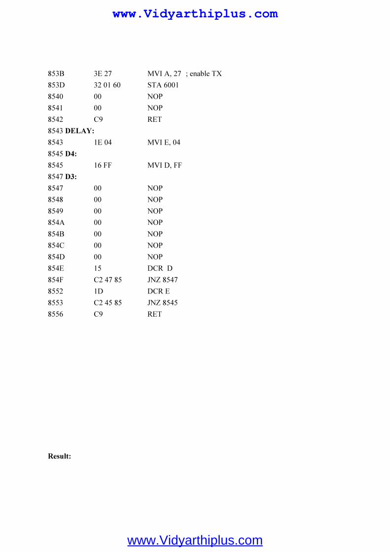
8545 3E 27 MVI A, 27 ; enable TX
8547 32 01 60 STA 6001
854A 00 NOP
854B 00 NOP
854C C9 RET
854D DELAY:
854D 1E 04 MVI E, 04
854F D4:
854F 16 FF MVI D, FF
8551 D3:
8551 00 NOP
8552 00 NOP
8553 00 NOP
8554 00 NOP
8555 00 NOP
8556 00 NOP
8557 00 NOP
8558 15 DCR D
www.Vidyarthiplus.com
www.Vidyarthiplus.com

8559 C2 51 85 JNZ 8551
855C 1D DCR E
855D C2 4F 85 JNZ 854F
8560 C9 RET
RECEIVER PROGRAM:
8500 CD 13 85 CALL 8513 ;initthecounter1togenerate2400Baud Rate
8503 CD 07 85 CALL 8507
8506 CF RST 1
8507 RXBYTE:
8507 WWW:
8507 3A 01 60 LDA 6001 ;check with the receive over flag
850A E6 02 ANI 02
850C CA 07 85 JZ 8507
850F 3A 00 60 LDA 6000 ; Get the Received Byte
8512 C9 RET
8513 BAUDINIT:
8513 3E 77 MVI A, 77 ; counter1 is selected
8515 D3 13 OUT 13 ; out DX, AL
8517 3E 78 MVI A, 78 ; count LSB
8519 D3 11 OUT 11 ; counter1 reg
851B 3E 00 MVI A, 00
851D D3 11 OUT 11 ; count MSB
851F 00 NOP
8520 00 NOP
8521 3E 00 MVI A, 00 ; Dummy word
8523 32 01 60 STA 6001 ; Status register
8526 32 01 60 STA 6001
8529 32 01 60 STA 6001
852C 3E 40 MVI A, 40 ; Reset word
852E 32 01 60 STA 6001
8531 CD 43 85 CALL 8543
8534 3E 4E MVI A, 4E
8536 32 01 60 STA 6001
8539 00 NOP
853A 00 NOP
www.Vidyarthiplus.com
www.Vidyarthiplus.com
853B 3E 27 MVI A, 27 ; enable TX
853D 32 01 60 STA 6001
8540 00 NOP
8541 00 NOP
8542 C9 RET
8543 DELAY:
8543 1E 04 MVI E, 04
8545 D4:
8545 16 FF MVI D, FF
8547 D3:
8547 00 NOP
8548 00 NOP
8549 00 NOP
854A 00 NOP
854B 00 NOP
854C 00 NOP
854D 00 NOP
854E 15 DCR D
854F C2 47 85 JNZ 8547
8552 1D DCR E
8553 C2 45 85 JNZ 8545
8556 C9 RET
Result:
www.Vidyarthiplus.com
www.Vidyarthiplus.com

Ex.No : 11
Date :
TRAFFIC LIGHT CONTROLLER
Aim:
Program:
PPI: equ 20h ;top 8255 address (in vik-85L kit)
ORG 9000H
MVI A,80H ;ALL PORTS AS O/P
OUT PPI+3
;-----------------------------------------------------------------
;FOR STARTING VEHICLES N-S DIRECTION(STARIGHT)&PEDESTRIAN STOPPING
;-----------------------------------------------------------------
CONTINUE:
MVI A,0FH ;FOR PEDESTRIAN
OUT PPI+1 ;SIGNAL
MVI A,4DH ;FOR GREEN LEDS IN N-S
OUT PPI ;DIRECTION
CALL DELAY ;SEQUENCE DELAY
CALL AMBER ;AMBER DELAY
;-----------------------------------------------------------------
;FOR STOPING VEHICLES IN N-S DIRECTION & STARTING IN E-W DIRECTION
;-----------------------------------------------------------------
;FOR STOPPING N-S SIDES&
MVI A,8BH ;STARTING E-W SIDES
OUT PPI
CALL DELAY ;SEQUENCE DELAY
CALL AMBER ;AMBER DELAY
;-----------------------------------------------------------------
;FOR STARIGHT RIGHT TURN IN N-S SIDES& STOPING E-W SIDES
;-----------------------------------------------------------------
www.Vidyarthiplus.com
www.Vidyarthiplus.com

MVI A,4DH ;FOR FREE LEFT IN ALL SIDES
OUT PPI ;& STOPPING IN E-W SIDES
;FOR RIGHT TURN IN N-S SIDES
MVI A,0 ;NO RIGHT TURN FROM SOUTH & FROM NORTH
OUT PPI+2
CALL DELAY ;SEQUENCE DELAY
MVI A,0 ;FOR AMPER
OUT PPI+2 ;SIGNAL
CALL AMBER ;FOR AMPER DELAY
;-----------------------------------------------------------------
;STOPING RIGHT TURN IN N-S SIDES & STARTING RIGHT TURN IN E-W SIDES
;-----------------------------------------------------------------
MVI A,8BH ;FOR STOPPING VEHICLES
OUT PPI ;IN N-S SIDES ;
;FOR RIGHT TURN IN
MVI A,0 ;E-W SIDES; NO RIGHT FROM EAST AND WEST
OUT PPI+2
CALL DELAY ;SEQUENCE DELAY
MVI A,0
OUT PPI+2
MVI A,30H
OUT PPI
MVI B,4
CALL DELAYSUB ;FOR AMBER DELAY
;-----------------------------------------------------------------
;FOR STARTING PEDESTRIAN
;-----------------------------------------------------------------
MVI A,0C0H ;FOR STOPPING VEHICLE
OUT PPI ;IN ALL SIDES
;GREEN SIGNAL FOR
MVI A,0F0H ;PEDESTRIAN
OUT PPI+1
MVI B,10H ;DELAY FOR PEDESTRIAN
www.Vidyarthiplus.com
www.Vidyarthiplus.com

CALL DELAYSUB
MVI A,30H
OUT PPI
MVI B,8
CALL DELAYSUB ;AMBER DELAY
JMP CONTINUE
AMBER:
;FOR AMBER SIGNAL
MVI A,39H ;IN ALL SIDES
OUT PPI
MVI B,8H ;DEALY COUNT
CALL DELAYSUB
RET
DELAY:
MVI B,40H ;DELAY COUNT FOR GREEN&
CALL DELAYSUB ;RED SIGNALS
RET
DELAYSUB:
;DELAY ROUTINE
;R1 * .5SEC
BACK2:
MVI C,0FFH
BACK1:
MVI A,0FFH
BACK:
NOP
DCR A
www.Vidyarthiplus.com
www.Vidyarthiplus.com

JNZ BACK
DCR C
JNZ BACK1
MOV A,B
ORA B
JZ OUT
DCR B
JNZ BACK2
OUT: RET
Diagram:
Result:
www.Vidyarthiplus.com
www.Vidyarthiplus.com

EX.NO.12.A 8-BIT ADDITION AND SUBTRACTION USING 8051
DATE:
AIM:
To write an assembly language program for 8-bit addition and subtraction
using 8051.
APPARATUS REQUIRED:
1) 8051 micro controller
2) Power supply unit
ALGORITHM (ADDITION):
1) Start the program
2) Get the data
3) Add two numbers
4) Store the result
5) Stop the program
ALGORITHM (SUBTRACTION):
1) Start the program
2) Get the data
3) Subtract two numbers
4) Store the result
5) Stop the program
www.Vidyarthiplus.com
www.Vidyarthiplus.com

Program (addition):
ADDRESS LABEL MNEMONICS COMMENTS
9100 START CLR C
MOV R0, #00
MOV A,#05
MOV B,#03
ADD A,B
MOV DPTR,#9200
JNC AHEAD
INC R0
AHEAD MOV X @DPTR,A
INC DPTR
MOV A,R0
MOV X @DPTR,A
HERE SJMP HERE
PROGRAM (SUBTRACTION):
ADDRESS LABEL MNEMONICS COMMENTS
9100 START CLR C
MOV R0, #00
MOV A,#05
MOV B,#03
SUBB A,B
MOV DPTR,#9200
JNC AHEAD
INC R0
AHEAD MOV X @DPTR,A
INC DPTR
MOV A,R0
MOV X @DPTR,A
HERE SJMP HERE
www.Vidyarthiplus.com
www.Vidyarthiplus.com

ADDITION:
DATA
INPUT
OUTPUT
SUBTRACTION:
DATA
INPUT
OUTPUT
RESULT:
www.Vidyarthiplus.com
www.Vidyarthiplus.com

EX: NO:12.B 8-BIT MULTIPLICATION AND DIVISION USING 8051
DATE:
AIM:
To write an assembly language program for 8-bit multiplication and division
using 8051.
APPARATUS REQUIRED:
1) 8051 microcontroller
2) Power supply
ALGORITHM (MULTIPLICATION):
1) Start the program
2) Get the two numbers
3) Multiply two numbers
4) Store the result
5) Stop the program
ALGORITHM (DIVISION):
1) Start the program
2) Get the two numbers
3) Multiply two numbers
4) Store the result
5) Stop the program
PROGRAM (MULTIPLICATION):
Address Label Mnemonics Opcode Comments
9000 START MOV A,#05 74,04
MOV F0,#03 75,F0,03
MUL AB A4
MOV DPTR,#9200 90,45,00
MOVX @ DPTR,A F0
INC DPTR A3
MOV A,F0 E5,F0
MOVX @DPTR,A F0
HERE SJMP HERE 80,FE
www.Vidyarthiplus.com
www.Vidyarthiplus.com

PROGRAM (DIVISION):
Address Label Mnemonics Opcode Comments
9000 START MOV A,#05 74,04
MOV F0,#03 75,F0,03
DIV AB A4
MOV DPTR,#9200 90,45,00
MOVX @ DPTR,A F0
INC DPTR A3
MOV A,F0 E5,F0
MOVX @DPTR,A F0
HERE SJMP HERE 80,FE
MULTIPLICATION DIVISION
INPUT
OUTPUT
RESULT:
www.Vidyarthiplus.com
www.Vidyarthiplus.com

Ex.No :13
Date :
CALLING SUBROUTINE
( 8051 - SUM USING CALL OPTION )
AIM:
To find the sum of elements in an array using call option.
ALGORITHM:
1. Start
2. Move the data to DPTR
3. Move the data to accumulator
4. Adjacent call 9200
5. Add A & R0
6. Move the 16 bit data from A to DPTR
7. Move the data to accumulator
8. Move the data to R0
9. Return to 4107
Program:
9000: MOV DPTR,#9200
MOV R1, #05
ACALL 9200
MOVX @DPTR,A
HERE: SJMP HERE
9200: MOV A,#02
MOV R0, #01
LOOP1: ADD A,R0
DJNZ R1,LOOP1
RET
OUTPUT:
9200 - 03H
RESULT:
www.Vidyarthiplus.com
www.Vidyarthiplus.com

Ex.No :14
Date :
PROGRAMMING WITH 8051 – CONTROL OF STEPPER MOTOR
Aim:
To interface a stepper motor with 8051 microcontroller and operate it.
THEORY:
A motor in which the rotor is able to assume only discrete stationary angular position is a stepper motor. The rotary motion occurs in a step-wise manner from one equilibrium position to the next. Stepper Motors are used very wisely in position control systems like printers, disk drives, process control machine tools, etc.
The basic two-phase stepper motor consists of two pairs of stator poles. Each of the four poles has its own winding. The excitation of any one winding generates a North Pole. A South Pole gets induced at the diametrically opposite side. The rotor magnetic system has two end faces. It is a permanent magnet with one face as South Pole and the other as North Pole.
The Stepper Motor windings A1, A2, B1, B2 are cyclically excited with a DC current to run the motor in clockwise direction. By reversing the phase sequence as A1, B2, A2, B1, anticlockwise stepping can be obtained. 2-PHASE SWITCHING SCHEME: In this scheme, any two adjacent stator windings are energized. The switching scheme is shown in the table given below. This scheme produces more torque. ADDRESS DECODING LOGIC: The 74138 chip is used for generating the address decoding logic to generate the device select pulses, CS1 & CS2 for selecting the IC 74175.The 74175 latches the data bus to the stepper motor driving circuitry. Stepper Motor requires logic signals of relatively high power. Therefore, the interface circuitry that generates the driving pulses use silicon darlington pair transistors. The inputs for the interface circuit are TTL pulses generated under software control using the Microcontroller Kit. The TTL levels of pulse sequence from the data bus is translated to high voltage output pulses using a buffer 7407 with open collector.
www.Vidyarthiplus.com
www.Vidyarthiplus.com

Program:(8051)
org 8600h
;Program for rotating one motor in clockwise direction and
;the other in anti clockwise direction
start: MOV DPTR,#4003H ;CONTROL PORT OF 8255
MOV A,#80H
MOVX @DPTR,A ;ALL BITS OUTPUTS
MOV DPTR,#4000H
LOOP: MOV A,#0A0H ;0A6H ;FIRST STEP SEQUENCE
MOVX @DPTR,A
LCALL DELAY ;DELAY BEFORE ISSUING THE NEXT STEP
COMMAND
MOV A,#0E0H ;0E7H ;SECOND STEP SEQUENCE
MOVX @DPTR,A
LCALL DELAY ;DELAY
MOV A,#0C0H ;0C5H ;THIRD STEP SEQUENCE
MOVX @DPTR,A
LCALL DELAY ;DELAY
MOV A,#80H ;84H ;FOURTH SEQUENCE
MOVX @DPTR,A
www.Vidyarthiplus.com
www.Vidyarthiplus.com

LCALL DELAY ;DELAY
LJMP LOOP ;REPEAT
;TO CHANGE THE PROGRAM FOR ROTATING IN
CLOCKWISE DIRECTION
;CHANGE A6 TO A5 AND CHANGE C5 TO C6
DELAY:
MOV R1,#0AH
LAB1:
MOV A,#40H
LAB2:
NOP
NOP
NOP
NOP
DEC A
JNZ LAB2
DJNZ R1,LAB1
RET
RESULT:
www.Vidyarthiplus.com
www.Vidyarthiplus.com

Ex.No :15
Date :
PROGRAMMING WITH 8051 – DAC
Aim:
PORT DETAILS FOR 8051:
8255 control register address - 4003H
8255 Port A address - 4000H
8255 Port B address - 4001H
8255 Port C address - 4002H
DAC PROGRAM FOR 8051:
User can give the 8-bit digital data I\P, user can view the output at DAC O\P, which is from 2nd
pin of DAC (0800), Measure the output voltage using digital Multimeter.
www.Vidyarthiplus.com
www.Vidyarthiplus.com

8500 90 40 03 MOV DPTR,#4003 ; CONTROL REGISTER ADDRESS
8503 74 80 MOV A, #80 ; 8255 CNTRL WORD (ALL PORTS
ARE O/P)
8505 F0 MOVX @DPTR, A ; ALL PORTS AS O\P
8506 74 00 MOV A, #00 ; DIGITAL INPUT DATA1
8508 90 40 00 MOV DPTR, #4000
850B F0 MOVX @DPTR, A ; DIGITAL DATA TO PORT A
850C 74 80 MOV A, #80 ; DIGITAL INPUT DATA2
850E 90 40 01 MOV DPTR, #4001
8511 F0 MOVX @DPTR, A ; DIGITAL DATA TO PORT B
8512 90 40 02 MOV DPTR, #4002
8515 74 00 MOV A, #00 ; DAC SELECTION DATA
(00 OR 01)
8517 F0 MOVX @DPTR, A ; DIGITAL DATA TO PORT C
8518 12 00 BB LCALL 00BB
CALCULATION:
1 count (decimal) = VCC / 256
= 5/ 256
= 0.0196v
RESULT:
Digital input output voltage
00 0.0
19 0.5
33 1.0
4C 1.5
66 2.0
7f 2.5
99 3.0
www.Vidyarthiplus.com
www.Vidyarthiplus.com

B2 3.5
CC 4.0
E5 4.5
FF 5.0
WORKING PROCEDURE FOR DAC :
Connect the 9 pin D type connector from the DAC module to the Mp/Mc kit.
Connect the 26-pin connector from the DUAL CHANNEL DAC module to Mp/Mc kit.
Connect the keyboard to the Mp/Mc kit.
Switch on the power supply.
Assemble your program.
Execute it and measure the output voltage at the front panel of the DAC module.
Vary the digital count, execute the program and measure the output analog voltage.
Take number of readings and if required draws the graph, DAC input count Vs output
voltage to check the linearity.
Switch off the power supply and remove all the connections.
RESULT:
www.Vidyarthiplus.com
www.Vidyarthiplus.com
Ex. No: 16
Date :
STUDY OF BASIC LOGIC GATES
AIM:
To Study the basic logic gates and also verify the truth table.
APPARATUS REQUIRED:
S.No Components
Required Range Quantity
1. OR GATE IC7432 1
2. AND GATE IC 7408 1
3. NOT GATE IC7404 1
4. NAND GATE IC7400 1
5. NOR GATE IC7402 1
6. EXOR GATE IC7486 1
7. Digital Trainer Kit (0-12) V 1
8. Connecting Wires - -
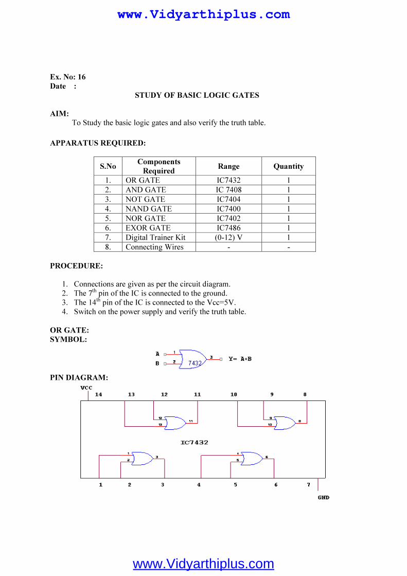
PROCEDURE:
1. Connections are given as per the circuit diagram. 2. The 7th pin of the IC is connected to the ground. 3. The 14th pin of the IC is connected to the Vcc=5V.
4. Switch on the power supply and verify the truth table.
OR GATE:
SYMBOL:
PIN DIAGRAM:
www.Vidyarthiplus.com
www.Vidyarthiplus.com

TRUTH TABLE:
INPUT OUTPUT
A B Y
0 0 0
0 1 1
1 0 1
1 1 1
AND GATE:
SYMBOL:
PINDIAGRAM:
TRUTH TABLE:
INPUT OUTPUT
A B Y
0 0 0
0 1 0
1 0 0
1 1 1
NOT GATE:
SYMBOL:
www.Vidyarthiplus.com
www.Vidyarthiplus.com

PINDIAGRAM:
TRUTH TABLE:
INPUT OUTPUT
A Y
0 1
1 0
NAND GATE:
SYMBOL:
PINDIAGRAM:
www.Vidyarthiplus.com
www.Vidyarthiplus.com

TRUTH TABLE:
INPUT OUTPUT
A B Y
0 0 1
0 1 1
1 0 1
1 1 0
NOR GATE:
SYMBOL:
PINDIAGRAM:
TRUTH TABLE:
INPUT OUTPUT
A B Y
0 0 1
0 1 0
1 0 0
1 1 0
EXOR GATE:
www.Vidyarthiplus.com
www.Vidyarthiplus.com

PINDIAGRAM:
TRUTH TABLE:
INPUT OUTPUT
A B Y
0 0 0
0 1 1
1 0 1
1 1 0
VIVA QUESTIONS:
1. Define gate. 2. What is the difference between gate and latch? 3. Draw the truth table for AND, OR, NOT.
RESULT:
www.Vidyarthiplus.com
www.Vidyarthiplus.com

Ex. No: 17
Date :
STUDY OF BASIC FLIP FLOPS
AIM
To construct RS,D and JK Flip-flop and verify their truth table.
APPARATUS REQUIRED
S.NO COMPONENTS SPECIFICATION QUANTITY
1 2 3
4
NAND Gate NOR Gate 3i/p AND Gate Digital Trainer Kit
IC 7411 IC 7402 IC 7411
(0-12)V
1 1 1 1
PROCEDURE
1. Design the circuit from the given specification.
2. Connections are given as per the Logic diagram.
3. Inputs are given as per the truth table.
4. Switch on the power supply and verify the truth table.
RS FLIP FLOP
LOGIC SYMBOL
Q
Q
S
R
LOGIC DIAGRAM
www.Vidyarthiplus.com
www.Vidyarthiplus.com

TRUTH TABLE
R S Q
STATE
0 0 1 1
0 1 0 1
NC 1 0 1/0
NC 1 1 0/1
No Change Set Reset Indeterminate
D FLIP FLOP
LOGIC SYMBOL
LOGIC DIAGRAM
TRUTH TABLE
CP D Qn+1
0 1 1
X 0 1
Qn
0 1
JK FLIP FLOP (LOGIC SYMBOL)
www.Vidyarthiplus.com
www.Vidyarthiplus.com

LOGIC DIAGRAM
3
4
5
6
11
10
9
8
2
3
1
5
6
4 Q
Q
S
R
J
K
CP
TRUTH TABLE
Qn J K Qn+1
0 0 0 0 1 1 1 1
0 0 1 1 0 0 1 1
0 1 0 1 0 1 0 1
0 0 1 1 1 0 1 0
RESULT
Prepared by C.GOKUL,AP/EEE
www.Vidyarthiplus.com
www.Vidyarthiplus.com
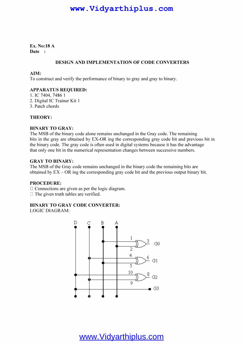
Ex. No:18 A
Date :
DESIGN AND IMPLEMENTATION OF CODE CONVERTERS
AIM:
To construct and verify the performance of binary to gray and gray to binary.
APPARATUS REQUIRED:
1. IC 7404, 7486 1 2. Digital IC Trainer Kit 1 3. Patch chords
THEORY:
BINARY TO GRAY:
The MSB of the binary code alone remains unchanged in the Gray code. The remaining bits in the gray are obtained by EX-OR ing the corresponding gray code bit and previous bit in the binary code. The gray code is often used in digital systems because it has the advantage that only one bit in the numerical representation changes between successive numbers.
GRAY TO BINARY:
The MSB of the Gray code remains unchanged in the binary code the remaining bits are obtained by EX – OR ing the corresponding gray code bit and the previous output binary bit.
PROCEDURE:
F Connections are given as per the logic diagram. X The given truth tables are verified.
BINARY TO GRAY CODE CONVERTER:
LOGIC DIAGRAM:
www.Vidyarthiplus.com
www.Vidyarthiplus.com

TRUTH TABLE:
DECIMAL BINARY CODE GRAY CODE
D C B A G3 G2 G1 G0
0 0 0 0 0 0 0 0 0 1 0 0 0 1 0 0 0 1 2 0 0 1 0 0 0 1 1 3 0 0 1 1 0 0 1 0 4 0 1 0 0 0 1 1 0 5 0 1 0 1 0 1 1 1 6 0 1 1 0 0 1 0 1 7 0 1 1 1 0 1 0 0 8 1 0 0 0 1 1 0 0 9 1 0 0 1 1 1 0 1 10 1 0 1 0 1 1 1 1 11 1 0 1 1 1 1 1 0 12 1 1 0 0 1 0 1 0 13 1 1 0 1 1 0 1 1 14 1 1 1 0 1 0 0 1 15 1 1 1 1 1 0 0 0
GRAY TO BINARY CODE CONVERTER:
TRUTH TABLE:
G3 G2 G1 G0 B3 B2 B1 B0 0 0 0 0 0 0 0 0 1 1 1 1 1 1 1 1
0 0 0 0 1 1 1 1 1 1 1 1 0 0 0 0
0 0 1 1 1 1 0 0 0 0 1 1 1 1 0 0
0 1 1 0 0 1 1 0 0 1 1 0 0 1 1 0
0 0 0 0 0 0 0 0 1 1 1 1 1 1 1 1
0 0 0 0 1 1 1 1 0 0 0 0 1 1 1 1
0 0 1 1 0 0 1 1 0 0 1 1 0 0 1 1
0 1 0 1 0 1 0 1 0 1 0 1 0 1 0 1
www.Vidyarthiplus.com
www.Vidyarthiplus.com

KARNAUGH MAP:
LOGIC DIAGRAM:
PROCEDURE:
1) Connections are given as per the circuit diagram 2) Power supply is switched on and a supply of +5V is maintained 3) Input binary code values are given and its appropriative gray code values are checked
in the outputs G3, G2, G1 & G0 4) If an output bit is equal to 1, that output bits LED glows indicating logic 1 and it an
output bit is equal to 0, that output bit LED does not glow indicating logic 0 RESULT:
www.Vidyarthiplus.com
www.Vidyarthiplus.com

Ex. No: 18 B
Date :
DESIGN AND IMPLEMENTATION OF ENCODERS AND DECODERS
AIM: To verify the table of 2x4 decode and 4x2 encoder. APPARATUS REQUIRED:
S.No Components
Require Range Quantity
1. RPS +5V 1 2. Resistor 330Ω 4 3. LED --- 4
4.
IC’S
7432 1 7408 1 7404 1 7421 2
THEORY:
DECODER:
Discrete quantities are represented in digital systems with binary with binary codes. A binary code of n bits capable of representing up to 2n distinct elements of the coded information. A decoder is a combinational circuit that converts binary information from n input lines to a maximum of 2n unique output lines. If the n-bit decoded information has unused or don’t-care combination, the decoder output will have fewer than 2n outputs. As an example consider the 2 to 4 line decoder circuit. The 2 inputs are decoded into 4 outputs, each output representing one the minterms of the 2 input variables. The 2 inverters provide the complement of the inputs, and each one of the 4 AND gates generate one of the minterms. ENCODER:
An encoder is a digital circuit that performs the inverse operation of a decoder. An encoder has 2n input lines and n output lines, the output lines generate the binary code corresponding to the input value. An example of an encoder is the octal to binary encoder. It has eight inputs, one for each of the octal digits and the three outputs that generate the corresponding binary number. It is assumed that only one input has a value Of 1 at any given time; otherwise the circuit has no meaning. The circuit that is presented here is 4 x 2 encoder.
www.Vidyarthiplus.com
www.Vidyarthiplus.com

4:2 ENCODER:
TRUTH TABLE:
INPUT OUTPUT
D1 D2 D3 D4 X Y
1 0 0 0 0 0 0 1 0 0 0 1 0 0 1 0 1 0 0 0 0 1 1 1
KARNAUGH MAP:
CIRCUIT DIAGRAM:
74047432
7432
D1 D3 D2 D4
X= D3+D4
Y= D1’D3
www.Vidyarthiplus.com
www.Vidyarthiplus.com

2:4 DECODER:
TRUTH TABLE:
INPUT OUTPUT
X Y D1 D2 D3 D4
0 0 1 0 0 0 0 1 0 1 0 0 1 0 1 0 1 0 1 1 0 0 0 1
LOGIC DIAGRAM:
PROCEDURE:
• Check the components and IC’S before given the circuit connection. • Rig up the circuit as shown in fig. • Switch on power supply. • For logic 1connect the input to +5V and for logic 0, connect the input to ground. • Verify the truth table, if LED is glowing the output is 1 and if it is not output is zero. • Switch off the power supply.
RESULT:
www.Vidyarthiplus.com
www.Vidyarthiplus.com

Ex. No: 19
Date :
STUDY OF SHIFT REGISTERS
AIM:
To implement the following shift register using flip flop (i) SIPO (ii) SISO (iii) PISO (iv) PIPO APPARATUS REQUIRED:
S. No Name Specification Quantity 1. IC 7474 1 2. Digital IC Trainer Kit 1 3. Patch chords THEORY:
A register is used to move digital data. A shift register is a memory in which information is shifted from one position in to another position at a line when one clock pulse is applied. The data can be shifted either left or right direction towards right or towards left. A shift register can be used in four ways depending upon the input in which the data are entered in to and takes out of it. The four configuration are given as X Serial input – Serial output(SISO) X Parallel input – Serial output(PISO) X Serial input – Parallel output(SIPO) X Parallel input – Parallel output(PIPO) RS or JK flip flop are used to construct shift register have D flip flop is used for constructing shift register. PROCEDURE:
X Give the connections as per the circuit X Set or Reset at the pin 2 which it’s the MSB of serial data. X Apply a single clock Set or Reset second digital input at pin 2. X Repeat step 2 until all 4-bit data are taken away.
www.Vidyarthiplus.com
www.Vidyarthiplus.com

www.Vidyarthiplus.com
www.Vidyarthiplus.com

www.Vidyarthiplus.com
www.Vidyarthiplus.com

RESULT:
Thus the SISO, SIPO, PISO, PIPO shift registers were designed and implemented.
www.Vidyarthiplus.com
www.Vidyarthiplus.com

Ex. No: 20
Date :
STUDY OF ASYNCHRONOUS COUNTER
AIM:
To implement and verify the truth table of an asynchronous decade counter.
APPARATUS REQUIRED:
S.No Name of the Apparatus Range Quantity 1. Digital IC trainer kit 1 2. JK Flip Flop IC 7473 2 3. NAND gate IC 7400 1 4. Connecting wires As required
THEORY: Asynchronous decade counter is also called as ripple counter. In a ripple counter the
flip flop output transition serves as a source for triggering other flip flops. In other words the clock pulse inputs of all the flip flops are triggered not by the incoming pulses but rather by the transition that occurs in other flip flops. The term asynchronous refers to the events that do not occur at the same time. With respect to the counter operation, asynchronous means that the flip flop within the counter are not made to change states at exactly the same time, they do not because the clock pulses are not connected directly to the clock input of each flip flop in the counter. PIN DIAGRAM OF IC 7473:
www.Vidyarthiplus.com
www.Vidyarthiplus.com

PROCEDURE:
1. Connections are given as per the circuit diagrams. 2. Apply the input and verify the truth table of the counter. RESULT:
The truth table of the Asynchronous counter was hence verified.
www.Vidyarthiplus.com
www.Vidyarthiplus.com

Ex. No: 21
Date :
DESIGN AND IMPLEMENTATION OF ADDER/SUBTRACTOR
AIM:
To design and construct half adder, full adder, half subtractor and full subtractor
circuits and verify the truth table using logic gates.
APPARATUS REQUIRED:
S. No Name Specification Quantity
1. IC 7432, 7408, 7486, 7483 1
2. Digital IC Trainer Kit 1
3. Patch chords -
THEORY:
The most basic arithmetic operation is the addition of two binary digits. There are four possible elementary operations, namely,
0 + 0 = 0 0 + 1 = 1 1 + 0 = 1 1 + 1 = 102
The first three operations produce a sum of whose length is one digit, but when the last
operation is performed the sum is two digits. The higher significant bit of this result is called a carry and lower significant bit is called the sum.
HALF ADDER:
A combinational circuit which performs the addition of two bits is called half adder.
The input variables designate the augend and the addend bit, whereas the output variables produce the sum and carry bits.
FULL ADDER:
A combinational circuit which performs the arithmetic sum of three input bits is called
full adder. The three input bits include two significant bits and a previous carry bit. A full adder circuit can be implemented with two half adders and one OR gate.
www.Vidyarthiplus.com
www.Vidyarthiplus.com
HALF ADDER TRUTH TABLE:
S.No INPUT OUTPUT
A
B S
C
1. 0 0 0 0
2. 0 1 1 0
3. 1 0 1 0
4. 1 1 0 1
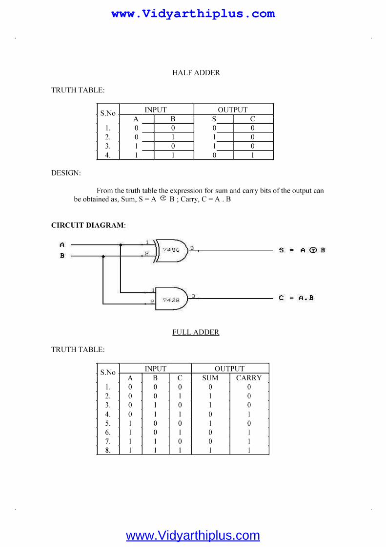
DESIGN:
From the truth table the expression for sum and carry bits of the output can be obtained as, Sum, S = A B ; Carry, C = A . B
CIRCUIT DIAGRAM:
FULL ADDER TRUTH TABLE:
S.No INPUT OUTPUT
A B C SUM CARRY
1. 0 0 0 0 0
2. 0 0 1 1 0
3. 0 1 0 1 0
4. 0 1 1 0 1
5. 1 0 0 1 0
6. 1 0 1 0 1
7. 1 1 0 0 1
8. 1 1 1 1 1
www.Vidyarthiplus.com
www.Vidyarthiplus.com

DESIGN:
From the truth table the expression for sum and carry bits of the output can be obtained
as,SUM = A’B’C + A’BC’ + AB’C’ + ABC;CARRY = A’BC + AB’C + ABC’ +ABC Using Karnaugh maps the reduced expression for the output bits can be obtained as, SUM
SUM = A’B’C + A’BC’ + AB’C’ + ABC = A B C CARRY
CARRY = AB + AC + BC CIRCUIT DIAGRAM:
www.Vidyarthiplus.com
www.Vidyarthiplus.com

HALF SUBTRACTOR:
A combinational circuit which performs the subtraction of two bits is called half subtractor. The input variables designate the minuend and the subtrahend bit, whereas the output variables produce the difference and borrow bits. FULL SUBTRACTOR:
A combinational circuit which performs the subtraction of three input bits is called full subtractor. The three input bits include two significant bits and a previous borrow bit. A full subtractor circuit can be implemented with two half subtractors and one OR gate.
HALF SUBTRACTOR TRUTH TABLE:
S.No INPUT OUTPUT
A B DIFF BORR
1. 0 0 0 0
2. 0 1 1 1
3. 1 0 1 0
4. 1 1 0 0
DESIGN:
From the truth table the expression for difference and borrow bits of the output can be obtained as, Difference, DIFF = A B; Borrow, BORR = A’ . B CIRCUIT DIAGRAM:
www.Vidyarthiplus.com
www.Vidyarthiplus.com

FULL SUBTRACTOR TRUTH TABLE:
S.No INPUT OUTPUT
A B C DIFF BORR
1. 0 0 0 0 0
2. 0 0 1 1 1
3. 0 1 0 1 1
4. 0 1 1 0 1
5. 1 0 0 1 0
6. 1 0 1 0 0
7. 1 1 0 0 0
8. 1 1 1 1 1
DESIGN:
From the truth table the expression for difference and borrow bits of the output can be obtained as,
Difference, DIFF= A’B’C + A’BC’ + AB’C’ + ABC Borrow, BORR = A’BC + AB’C + ABC’ +ABC
Using Karnaugh maps the reduced expression for the output bits can be obtained as,
DIFFERENCE
DIFF = A’B’C + A’BC’ + AB’C’ + ABC = A B C BORROW
BORR = A’B + A’C + BC
www.Vidyarthiplus.com
www.Vidyarthiplus.com

CIRCUIT DIAGRAM:
PROCEDURE:
The connections are given as per the circuit diagram. Two 4 – bit numbers added or subtracted depend upon the control input and
the output is obtained.
Apply the inputs and verify the truth table for thehalf adder or s subtractor and full adder or subtractor circuits.
RESULT:
Thus the half adder, full adder, half subtractor and full subtractor circuits were designed and their truth table were verified.
www.Vidyarthiplus.com
www.Vidyarthiplus.com

Ex. No: 22 Date :
DESIGN AND TESTING OF INTEGRATOR AND DIFFERENTIATOR
DIFFERENTIATOR
AIM: To design a Differentiator circuit for the given specifications using Op-Amp IC 741.
APPARATUS REQUIRED:
S.No Name of the Apparatus Range Quantity
1. Function Generator 3 MHz 1 2. CRO 30 MHz 1 3. Dual RPS 0 – 30 V 1 4. Op-Amp IC 741 1 5. Bread Board 1 6. Resistors
7. Capacitors
8. Connecting wires and probes As required
THEORY:
The differentiator circuit performs the mathematical operation of differentiation; that is, the output waveform is the derivative of the input waveform. The differentiator may be constructed from a basic inverting amplifier if an input resistor R1 is replaced by a capacitor
C1. The expression for the output voltage is given as, Vo = - Rf C1 (dVi /dt) Here the negative sign indicates that the output voltage is 180
0 out of phase with the
input signal. A resistor Rcomp = Rf is normally connected to the non-inverting input terminal of the op-amp to compensate for the input bias current. A workable differentiator can be designed by implementing the following steps:
1. Select fa equal to the highest frequency of the input signal to be differentiated. Then, assuming a value of C1 < 1 µF, calculate the value of R f.
2. Choose fb = 20 fa and calculate the values of R1 and Cf so that R1C1 = Rf Cf. 3. The differentiator is most commonly used in waveshaping circuits to detect high
frequency components in an input signal and also as a rate–of–change detector in FM modulators.
www.Vidyarthiplus.com
www.Vidyarthiplus.com

CIRCUIT DIAGRAM OF DIFFERENTIATOR: DESIGN:
Given fa = --------------- We know the frequency at which the gain is 0 dB, fa = 1 / (2π Rf C1) Let us assume C1 = 0.1 µF; then Rf = _________ Since fb = 20 fa, fb = --------------- We know that the gain limiting frequency fb = 1 / (2π R1 C1) Hence R1 = _________ Also since R1C1 = Rf Cf ; Cf = _________
PROCEDURE: 1. Connections are given as per the circuit diagram. 2. + Vcc and - Vcc supply is given to the power supply terminal of the Op-Amp IC. 3. By adjusting the amplitude and frequency knobs of the function generator, appropriate
input voltage is applied to the inverting input terminal of the Op-Amp. 4. The output voltage is obtained in the CRO and the input and output voltage waveforms
are plotted in a graph sheet.
OBSERVATIONS:
Input - Sine wave
S.No. Amplitude Time period ( No. of div x Volts per div ) ( No. of div x Time per div )
Input
Output Input – Square wave
S.No. Amplitude Time period ( No. of div x Volts per div ) ( No. of div x Time per div )
Input
Output
www.Vidyarthiplus.com
www.Vidyarthiplus.com

DIFFERENTIATOR:
INPUT SIGNAL:
Amplitude
Time Period
OUTPUT SIGNAL:
Amplitude
Time Period
INTEGRATOR
APPARATUS REQUIRED: S.No Name of the Apparatus Range Quantity
1. Function Generator 3 MHz 1 2. CRO 30 MHz 1 3. Dual RPS 0 – 30 V 1 4. Op-Amp IC 741 1 5. Bread Board 1 6. Resistors
7. Capacitors
8. Connecting wires and probes As required
THEORY:
A circuit in which the output voltage waveform is the integral of the input voltage waveform is the integrator. Such a circuit is obtained by using a basic inverting amplifier
www.Vidyarthiplus.com
www.Vidyarthiplus.com

configuration if the feedback resistor Rf is replaced by a capacitor Cf . The expression for the output voltage is given as,
Vo = - (1/Rf C1) ∫ Vi dt
Here the negative sign indicates that the output voltage is 180 0 out of phase with the
input signal. Normally between fa and fb the circuit acts as an integrator. Generally, the value of fa < fb . The input signal will be integrated properly if the Time period T of the signal is larger than or equal to Rf Cf. That is,
T ≥ Rf Cf
The integrator is most commonly used in analog computers and ADC and signal-wave shaping circuits.
PIN DIAGRAM: CIRCUIT DIAGRAM OF INTEGRATOR: DESIGN:
We know the frequency at which the gain is 0 dB, fb = 1 / (2π R1 Cf) Therefore fb = _____ Since fb = 10 fa, and also the gain limiting frequency fa = 1 / (2π Rf Cf) We get, Rf = _______ and hence R1 = __________
PROCEDURE:
1. Connections are given as per the circuit diagram. 2. + Vcc and - Vcc supply is given to the power supply terminal of the Op-Amp IC. 3. By adjusting the amplitude and frequency knobs of the function generator, appropriate
input voltage is applied to the inverting input terminal of the Op-Amp.
www.Vidyarthiplus.com
www.Vidyarthiplus.com

4. The output voltage is obtained in the CRO and the input and output voltage waveforms
are plotted in a graph sheet.
OBSERVATIONS:
S.No. Amplitude Time period
( No. of div x Volts per div ) ( No. of div x Time per div ) Input
Output
MODEL GRAPH:
INTEGRATOR:
INPUT SIGNAL:
Am
pli
tud
e
OUTPUT SIGNAL:
RESULT:
The design of the Differentiator & Integrator circuit was done and the input and output waveforms were obtained.
www.Vidyarthiplus.com
www.Vidyarthiplus.com

EX.No.23 ASTABLE AND MONOSTABLE MULTIVIBRATOR
DATE: USING NE555 TIMER
AIM:
To construct
a) Astable Multivibrator and
b) Monostable Multivibrator using IC 555 timer
To design an astable multivibrator circuit for the given specifications using 555 Timer
IC.
APPARATUS REQUIRED:
S. No Name of the Apparatus Range Quantity 1. Function Generator 3 MHz 1 2. CRO 30 MHz 1 3. Dual RPS 0 – 30 V 1 4. Timer IC IC 555 1 5. Bread Board 1 6. Resistors
7. Capacitors
8. Connecting wires and probes As required
THEORY:
An astable multivibrator, often called a free-running multivibrator, is a rectangular-wave-generating circuit. This circuit do not require an external trigger to change the state of the output. The time during which the output is either high or low is determined by two resistors and a capacitor, which are connected externally to the 555 timer. The time during which the capacitor charges from 1/3 Vcc to 2/3 Vcc is equal to the time the output is high and is given by,
tc = 0.69 (R1 + R2) C
Similarly the time during which the capacitor discharges from 2/3 Vcc to 1/3 Vcc is
equal to the time the output is low and is given by,
td = 0.69 (R2) C
Thus the total time period of the output waveform is,
T = tc + td = 0.69 (R1 + 2 R2) C
The term duty cycle is often used in conjunction with the astable multivibrator. The duty cycle is the ratio of the time tc during which the output is high to the total time period T. It is generally expressed in percentage. In equation form,
www.Vidyarthiplus.com
www.Vidyarthiplus.com
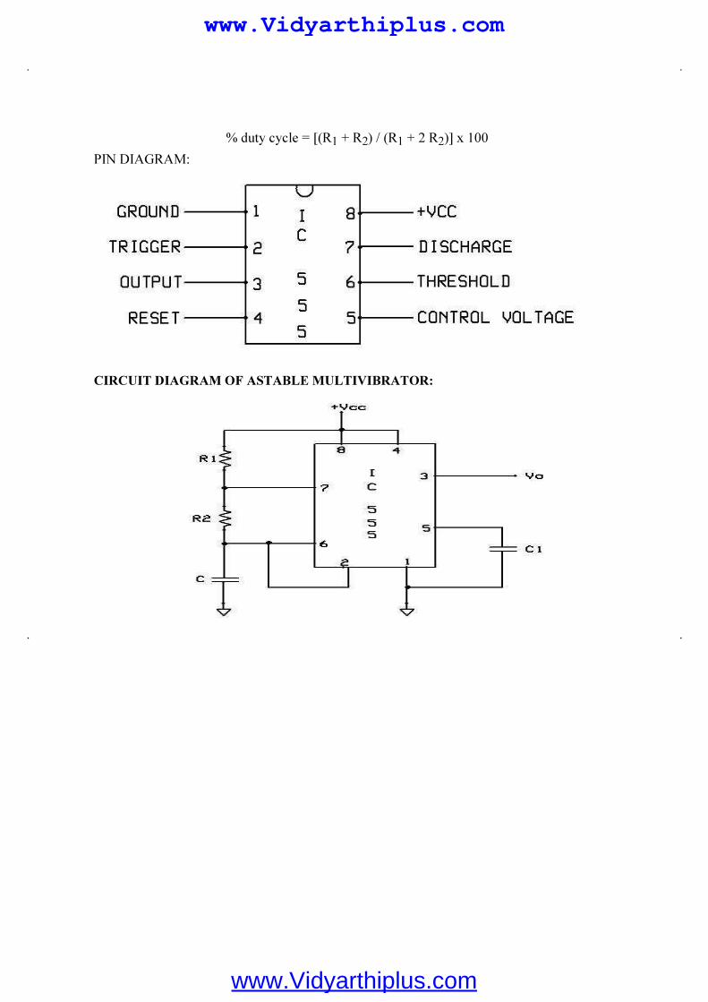
% duty cycle = [(R1 + R2) / (R1 + 2 R2)] x 100 PIN DIAGRAM: CIRCUIT DIAGRAM OF ASTABLE MULTIVIBRATOR:
www.Vidyarthiplus.com
www.Vidyarthiplus.com

DESIGN:
Given f= 4 KHz, Therefore, Total time period, T = 1/f = ____________
We know, duty cycle = tc / T Therefore, tc = ------------------------ and td = ____________
We also know for an astable multivibrator td = 0.69 (R2) C Therefore, R2 = _____________
tc = 0.69 (R1 + R2) C Therefore, R1 = _____________
PROCEDURE:
1. Connections are given as per the circuit diagram. 2. + 5V supply is given to the + Vcc terminal of the timer IC. 3. At pin 3 the output waveform is observed with the help of a CRO 4. At pin 6 the capacitor voltage is obtained in the CRO and the V0 and Vc voltage
waveforms are plotted in a graph sheet.
OBSERVATIONS:
Amplitude
S.No Waveforms ( No. of div x
Volts per div )
Time period (
No. of div x
Time per div )
tc td 1. Output Voltage , Vo
2. Capacitor voltage , Vc
www.Vidyarthiplus.com
www.Vidyarthiplus.com

MODEL GRAPH:
O/pvo
lta
ge
Vcc
T (ms)
2/3 Vcc
Capacitorvoltage 1/3 Vcc
TON
TOFF
RESULT:
The design of the Astable multivibrator circuit was done and the output voltage and capacitor voltage waveforms were obtained.
www.Vidyarthiplus.com
www.Vidyarthiplus.com
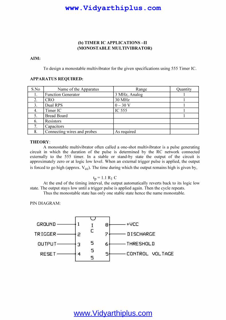
(b) TIMER IC APPLICATIONS –II (MONOSTABLE MULTIVIBRATOR)
AIM:
To design a monostable multivibrator for the given specifications using 555 Timer IC.
APPARATUS REQUIRED:
S.No Name of the Apparatus Range Quantity
1. Function Generator 3 MHz, Analog 1 2. CRO 30 MHz 1 3. Dual RPS 0 – 30 V 1 4. Timer IC IC 555 1 5. Bread Board 1 6. Resistors
7. Capacitors
8. Connecting wires and probes As required
THEORY:
A monostable multivibrator often called a one-shot multivibrator is a pulse generating circuit in which the duration of the pulse is determined by the RC network connected externally to the 555 timer. In a stable or stand-by state the output of the circuit is approximately zero or at logic low level. When an external trigger pulse is applied, the output is forced to go high (approx. Vcc). The time during which the output remains high is given by,
tp = 1.1 R1 C
At the end of the timing interval, the output automatically reverts back to its logic low state. The output stays low until a trigger pulse is applied again. Then the cycle repeats.
Thus the monostable state has only one stable state hence the name monostable.
PIN DIAGRAM:
www.Vidyarthiplus.com
www.Vidyarthiplus.com

CIRCUIT DIAGRAM OF MONOSTABLE MULTIVIBRATOR: DESIGN:
Given tp = 0.616 ms = 1.1 R1 C Therefore, R1 = _____________
PROCEDURE:
1. Connections are given as per the circuit diagram. 2. + 5V supply is given to the + Vcc terminal of the timer IC. 3. A negative trigger pulse of 5V, 2 KHz is applied to pin 2 of the 555 IC 4. At pin 3 the output waveform is observed with the help of a CRO 5. At pin 6 the capacitor voltage is obtained in the CRO and the V0 and Vc voltage
waveforms are plotted in a graph sheet. OBSERVATIONS:
Amplitude ( No. of div x
S.No Volts per div )
Time period (
No. of div x
Time per div )
ton Toff 1. Trigger input
2. Output Voltage , Vo 3. Capacitor voltage , Vc
www.Vidyarthiplus.com
www.Vidyarthiplus.com

MODEL GRAPH:
RESULT:
The design of the Monostable multivibrator circuit was done and the input and output
waveforms were obtained.
www.Vidyarthiplus.com
www.Vidyarthiplus.com

Ex. No: 23
Date :
FREQUENCY MULTIPLIER USING PLL
AIM:
To construct and test the frequency multiplier using PLL 565
APPARATUS REQUIRED:
S.NO APPARATUS NAME RANGE QUANTITY
1. Regulated variable power
supply
(0-30) Volts 2
2. Signal generator 1MHz 1
3. CRO 20MHz 1
COMPONENTS REQUIRED:
S.NO COMPONENT NAME RANGE QUANTITY
1. Resistors 20KΩ,2KΩ,
4.7KΩ,10KΩ
Each Two
2. PLL
COUNTER
IC565
IC7490
1
3. Capacitors 0.01µF,
0.001µF,
10µF
1
4. TRANSISTOR 2N2222 1
THEORY:
In the frequency multiplier using PLL565, a divided by N network is inserted
between the VCO output and the phase comparator input. Since the output of the comparator
is locked to the input frequency fin, the VCO is running at a multiple of the input frequency.
Therefore in the locked state the VCO output frequency fo is given by,
fo= Nfin
PROCEDURE:
1. Rig up the circuit of frequency multiplier
2. Connect the signal generator output to the input terminal of PLL
3. Connect the CRO probes to display the input and output signals
4. Set the input signal at 1Vpp square wave at 1khz
5. Vary the VCO frequency by adjusting the 20KΩ potentiometer till the PLL is locked
www.Vidyarthiplus.com
www.Vidyarthiplus.com

6. Measure the output frequency, it should be 5 times that of the input frequency
7. Repeat the steps for different range of frequencies
TABULATION:
Vin=
fin (Hz) Multiple Factor
Designed Obtained
PIN DIAGRAM:
www.Vidyarthiplus.com
www.Vidyarthiplus.com

RESULT:
www.Vidyarthiplus.com
www.Vidyarthiplus.com

Ex. No: 24
Date :
CLIPPER & CLAMPER
POSITIVE & NEGATIVE CLIPPER A circuit which cutoff voltage above or below are both specified level is called
clipper. A clipper which removes a portion of positive half cycle of the input signal is called
positive clipper. A clipper circuit that removes the negative half cycle is called negative
clipper.
Figure (a) shows the circuit of a positive clipper. Itconsists of a diode D and a resistor R with
output taken across the resistor. During positive half cycle the input voltage, the terminal A is
positive with respect to B. This reverse biases the diode and it acts as an open switch.
Therefore all the applied voltage drops across the diode and none across the resistor. As a
result of this, there is no output voltage during the positive half cycle of the input voltage.
During the negative half cycle of the input voltage, the terminal B is positive with respect to
A. Therefore it forward biases the diode and it acts as a closed switch. Thus, there is no
voltage drop across diode. During negative half cycle of the input voltage. All the input
voltage is drop across the resistor as shown in the output waveform.
Figure (b) shows the waveform of the input voltage. During the positive half cycle of the
voltage, the terminal A is positive with respect to the terminal B. Therefore the diode is
forward biased; as a result all the input voltage appears across the resistor. During negative
half cycle of the input voltage, the terminal B is positive with respect to the terminal A.
Therefore the diode is reverse biased and hence there is no voltage drop across the resistor
during negative half cycle.
Prepared by C.GOKUL,AP/EEEwww.Vidyarthiplus.com
www.Vidyarthiplus.com

POSITIVE & NEGATIVE CLAMPER
Clamping Definition:
A circuit that places either the positive or negative peak of a signal at a desired D.C level is
known as a clamping. A clamping adds a D.C components to the signal and does not change
the shape or amplitude of the input signal.
Clampers:
1.Positive Clamper
Diode clamping circuit simply consits of a diode D and capacitor C as shown in below
Figure.
During the negative half cycle of the input voltage Vin the diode is forward biased and the
current flows through the circuit. As a result of this, the capacitor C is charged to a voltage
equal to the negative peak value i.e., _Vm. Once the capacitor is fully charged to -Vm it
cannot discharge because the diode cannot conduct in the reverse direction. It means that this
capacitor acts as a battery with an emf equal to the -Vm. The polarity of this voltage is such
that it adds to the input signal. Therefore the output voltage is equal to the sum of the A.C
input signal and the capacitor voltage Vm i.e., Vin + Vm.
2.Negative Clamper
If we change the polarity of the diode and capacitor, then the circuit become negative
clamper.
www.Vidyarthiplus.com
www.Vidyarthiplus.com

ADDITIONAL EXPERIMENTS(for University Lab Practical)
1. Add two 16-bit Numbers (using DAD instruction):
8100: LHLD 8200
XCHG
LHLD 8202
MVI C, 00
DAD D
JNC 800E
INR C
SHLD 8300
MOV A, C
STA 8302
HLT
MEMORY ADDRESS
DATA 1
(WITHOUT
CARRY)
DATA 2
(WITH
CARRY)
INPUT
8200H
8201H
8202H
8203H
45
23
34
12
FF
FF
01
00
OUTPUT
8300H(SUM-lower)
8301H(SUM-Higher)
8302H(CARRY)
79
35
00
00
00
01
2345 1st
data FFFF
1234 + 2nd
data 0001 +
-------- ------------
3579 ---SUM 00-CARRY 10000 sum-0000 carry 01
------- -----------------
RESULT:
www.Vidyarthiplus.com
www.Vidyarthiplus.com

2.Add Two 16-bit Numbers(without using DAD instruction):
8100: LHLD 8200 : Get first 16-bit number in HL
XCHG : Save first 16-bit number in DE
LHLD 8202 : Get second 16-bit number in HL
MOV A, E : Get lower byte of the first number
ADD L :add lower byte of the second number
MOV L, A : Store the result in L register
MOV A, D : Get higher byte of the first number
ADC H : add higher byte of second number with borrow
MOV H, A : Store l6-bit result in memory locations .
SHLD 8300 : Store l6-bit result in memory locations 8300H and 8301H.
MOV A, C
STA 8302 store the carry at 8302 memory location
HLT : Terminate program execution.
MEMORY ADDRESS
DATA 1
(WITHOUT
CARRY)
DATA 2
(WITH
CARRY)
INPUT
8200H
8201H
8202H
8203H
45
23
34
12
FF
FF
01
00
OUTPUT
8300H(SUM-lower)
8301H(SUM-Higher)
8302H(CARRY)
79
35
00
00
00
01
2345 1st
data FFFF
1234 + 2nd
data 0001 +
-------- ------------
3579 ---SUM 00-CARRY 10000 sum-0000 carry 01
------- -----------------
www.Vidyarthiplus.com
www.Vidyarthiplus.com

3.Subtract Two 16-bit Numbers:
8100: LHLD 8200 : Get first 16-bit number in HL
XCHG : Save first 16-bit number in DE
LHLD 8202 : Get second 16-bit number in HL
MOV A, E : Get lower byte of the first number
SUB L :subtract lower byte of the second number
MOV L, A : Store the result in L register
MOV A, D : Get higher byte of the first number
SBB H : subtract higher byte of second number with borrow
MOV H, A : Store l6-bit result in memory locations .
SHLD 8300 : Store l6-bit result in memory locations 8300H and 8301H.
MOV A, C
STA 8302 store the borrow at 8302 memory location
HLT : Terminate program execution.
MEMORY ADDRESS
DATA 1
(WITHOUT
CARRY)
DATA 2
(WITH
CARRY)
INPUT
8200H
8201H
8202H
8203H
45
23
34
12
34
12
45
23
OUTPUT
8300H(DIFF-lower)
8301H(DIFF-Higher)
8302H(Borrow)
79
35
00
FF
EE
01
2345 1st
data 1234
1234 - 2nd
data 2345 -
-------- ------------
1111 ---Difference 00-borrow EEFF -Difference 01-borrow
------- ------------
www.Vidyarthiplus.com
www.Vidyarthiplus.com

4. Multiplication of Two 16 bit in 8085:
8100: LHLD 8200
SPHL
LHLD 8202
XCHG
LXI H,0000
LXI B,0000
NEXT: DAD SP
JNC AHEAD
INX B
AHEAD: DCX D
MOV A,E
ORA D
JNZ NEXT
SHLD 8300H
MOV L,C
MOV H,B
SHLD 8302H
HLT
MEMORY ADDRESS
DATA 1
INPUT
8200H
8201H
8202H
8203H
03
00
05
00
OUTPUT
8300H
8301H
8302H
8303H
0F
00
00
00
0003
0005 X
-------
000F answer = 00 00 00 0F
-------
www.Vidyarthiplus.com
www.Vidyarthiplus.com

5. SUM OF N NUMBERS
LDA 8200
MOV B,A
LXI H, 8201
SUB A
MOV B,A
LOOP ADD M
JNC SKIP (810E)
INR B
SKIP INX H
DCR C
JNZ LOOP (8109)
STA 8400
MOV A,B
STA 8401
HLT
www.Vidyarthiplus.com
www.Vidyarthiplus.com

MODEL CALCULATION:
Change 4200 as address 8200 & 4400 as 8400
www.Vidyarthiplus.com
www.Vidyarthiplus.com

16 – BIT DIVISION OF TWO NUMBERS
www.Vidyarthiplus.com
www.Vidyarthiplus.com

DESIGN OF 4-BIT SYNCHRONOUS UP COUNTER
Binary 4-bit Synchronous Up Counter
It can be seen above, that the external clock pulses (pulses to be counted) are fed directly to
each of the J-K flip-flops in the counter chain and that both the J and K inputs are all tied
together in toggle mode, but only in the first flip-flop, flip-flop FFA (LSB) are they
connected HIGH, logic “1” allowing the flip-flop to toggle on every clock pulse. Then the
synchronous counter follows a predetermined sequence of states in response to the common
clock signal, advancing one state for each pulse.
The J and K inputs of flip-flop FFB are connected directly to the output QA of flip-flop FFA,
but the J and K inputs of flip-flops FFC and FFD are driven from separate AND gates which
are also supplied with signals from the input and output of the previous stage. These
additional AND gates generate the required logic for the JK inputs of the next stage.
If we enable each JK flip-flop to toggle based on whether or not all preceding flip-flop
outputs (Q) are “HIGH” we can obtain the same counting sequence as with the asynchronous
circuit but without the ripple effect, since each flip-flop in this circuit will be clocked at
exactly the same time.
Then as there is no inherent propagation delay in synchronous counters, because all the
counter stages are triggered in parallel at the same time, the maximum operating frequency of
this type of frequency counter is much higher than that for a similar asynchronous counter
circuit.
www.Vidyarthiplus.com
www.Vidyarthiplus.com

4-bit Synchronous Counter Waveform Timing Diagram.
Because this 4-bit synchronous counter counts sequentially on every clock pulse the resulting
outputs count upwards from 0 ( 0000 ) to 15 ( 1111 ). Therefore, this type of counter is also
known as a 4-bit Synchronous Up Counter.
However, we can easily construct a 4-bit Synchronous Down Counter by connecting the
AND gates to the Q output of the flip-flops as shown to produce a waveform timing diagram
the reverse of the above. Here the counter starts with all of its outputs HIGH ( 1111 ) and it
counts down on the application of each clock pulse to zero, ( 0000 ) before repeating again.
www.Vidyarthiplus.com
www.Vidyarthiplus.com
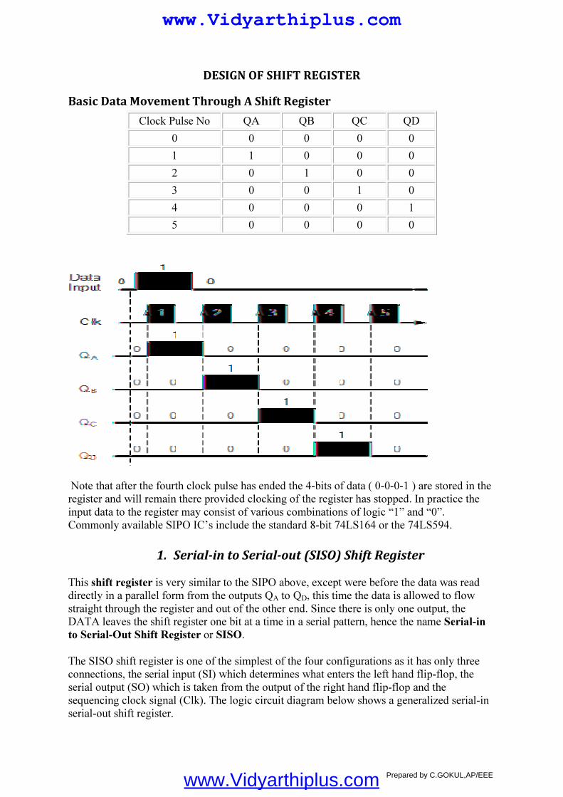
DESIGN OF SHIFT REGISTER
Basic Data Movement Through A Shift Register
Clock Pulse No QA QB QC QD
0 0 0 0 0
1 1 0 0 0
2 0 1 0 0
3 0 0 1 0
4 0 0 0 1
5 0 0 0 0
Note that after the fourth clock pulse has ended the 4-bits of data ( 0-0-0-1 ) are stored in the
register and will remain there provided clocking of the register has stopped. In practice the
input data to the register may consist of various combinations of logic “1” and “0”.
Commonly available SIPO IC’s include the standard 8-bit 74LS164 or the 74LS594.
1. Serial-in to Serial-out (SISO) Shift Register
This shift register is very similar to the SIPO above, except were before the data was read
directly in a parallel form from the outputs QA to QD, this time the data is allowed to flow
straight through the register and out of the other end. Since there is only one output, the
DATA leaves the shift register one bit at a time in a serial pattern, hence the name Serial-in
to Serial-Out Shift Register or SISO.
The SISO shift register is one of the simplest of the four configurations as it has only three
connections, the serial input (SI) which determines what enters the left hand flip-flop, the
serial output (SO) which is taken from the output of the right hand flip-flop and the
sequencing clock signal (Clk). The logic circuit diagram below shows a generalized serial-in
serial-out shift register.
Prepared by C.GOKUL,AP/EEEwww.Vidyarthiplus.com
www.Vidyarthiplus.com

4-bit Serial-in to Serial-out Shift Register
You may think what’s the point of a SISO shift register if the output data is exactly the same
as the input data. Well this type of Shift Register also acts as a temporary storage device or
as a time delay device for the data, with the amount of time delay being controlled by the
number of stages in the register, 4, 8, 16 etc or by varying the application of the clock pulses.
Commonly available IC’s include the 74HC595 8-bit Serial-in to Serial-out Shift Register all
with 3-state outputs.
2. Parallel-in to Serial-out (PISO) Shift Register
The Parallel-in to Serial-out shift register acts in the opposite way to the serial-in to parallel-
out one above. The data is loaded into the register in a parallel format in which all the data
bits enter their inputs simultaneously, to the parallel input pins PA to PD of the register. The
data is then read out sequentially in the normal shift-right mode from the register at Q
representing the data present at PA to PD.
This data is outputted one bit at a time on each clock cycle in a serial format. It is important
to note that with this type of data register a clock pulse is not required to parallel load the
register as it is already present, but four clock pulses are required to unload the data.
4-bit Parallel-in to Serial-out Shift Register
As this type of shift register converts parallel data, such as an 8-bit data word into serial
format, it can be used to multiplex many different input lines into a single serial DATA
stream which can be sent directly to a computer or transmitted over a communications line.
Commonly available IC’s include the 74HC166 8-bit Parallel-in/Serial-out Shift Registers.
Prepared by C.GOKUL,AP/EEE
www.Vidyarthiplus.com
www.Vidyarthiplus.com