Tracking Mobile Sensor Nodes in Wildlife Francine Lalooses Hengky Susanto EE194-Professor Chang.
EE194-EE290C - University of California, Berkeleyee290c/sp17/lectures/Lecture22.pdf · EE194-EE290C...
56
EE194-EE290C 28 nm SoC for IoT Ref: Communica:on Systems by A. Bruce Carlson, Paul B. Crilly and Janet C. Rutledge CMOS VLSI Design by Neil H. Weste and David Money Harris Timing Library Format Reference, Cadence Design System hSps://www.csee.umbc.edu/~cpatel2/links/641/slides/lect05_LIB.pdf Synopsys Design Compiler User Guide
Transcript of EE194-EE290C - University of California, Berkeleyee290c/sp17/lectures/Lecture22.pdf · EE194-EE290C...

EE194-EE290C28nmSoCforIoT
Ref:Communica:onSystemsbyA.BruceCarlson,PaulB.CrillyandJanetC.RutledgeCMOSVLSIDesignbyNeilH.WesteandDavidMoneyHarrisTimingLibraryFormatReference,CadenceDesignSystemhSps://www.csee.umbc.edu/~cpatel2/links/641/slides/lect05_LIB.pdfSynopsysDesignCompilerUserGuide

Synchroniza:onBitSynchroniza:onCarrierFrequencyandPhaseFrameSynchroniza:on

Synchroniza:onPNsequencegenerator.
m1 m2 m3 m4 m51 1 1 1 1
+
Output sequence
111010...

Synchroniza:onAutocorrela:onofaPNsequence.
τNTc
Tc
Rs(τ)1
-Tc(N-1)Tc (N+1)Tc
1/N

Synchroniza:onFrameSynchroniza:on
Preamble
Start ofmessage
Message bitst
Synchroniza:onFrameSynchroniza:on/PreambleDetec:on
aK aK-1 aK-2 aK-N...c1 c2 cn...
Σ VK
vk = cii=1
N
∑ ak−i

MatlabExample
openExample('comm/MSKSignalRecoveryExample')MSKSignalRecoveryExample
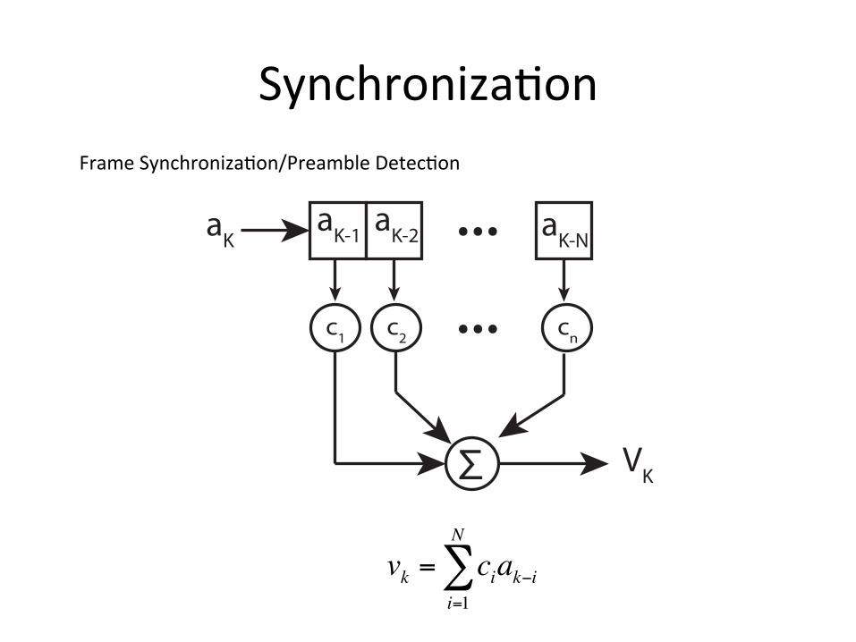
TransmissionGateMuxq Nonrestoring mux uses two transmission gates
- Only 4 transistors
S
S
D0
D1YS

DLatchq When CLK = 1, latch is transparent
- D flows through to Q like a buffer q When CLK = 0, the latch is opaque
- Q holds its old value independent of D q a.k.a. transparent latch or level-sensitive latch
CLK
D Q
Latch D
CLK
Q

DLatchDesignq Multiplexer chooses D or old Q
1
0
D
CLK
QCLK
CLKCLK
CLK
DQ Q
Q

DLatchOpera:on
CLK = 1
D Q
Q
CLK = 0
D Q
Q
D
CLK
Q

DFlip-flopFlop
CLK
D Q
D
CLK
Q
q When CLK rises, D is copied to Q q At all other times, Q holds its value q a.k.a. positive edge-triggered flip-flop, master-slave flip-flop
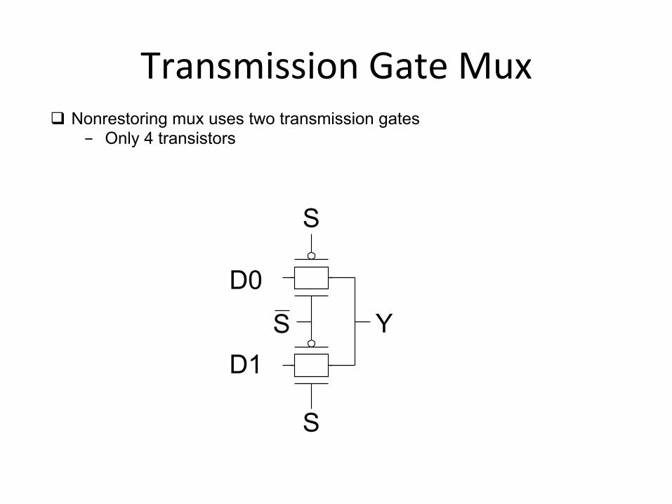
DFlip-flopDesignq Built from master and slave D latches
QMCLK
CLKCLK
CLK
Q
CLK
CLK
CLK
CLK
D
Latch
Latch
D QQM
CLK
CLK

DFlip-flopOpera:on
CLK = 1
D
CLK = 0
Q
D
QM
QMQ
D
CLK
Q
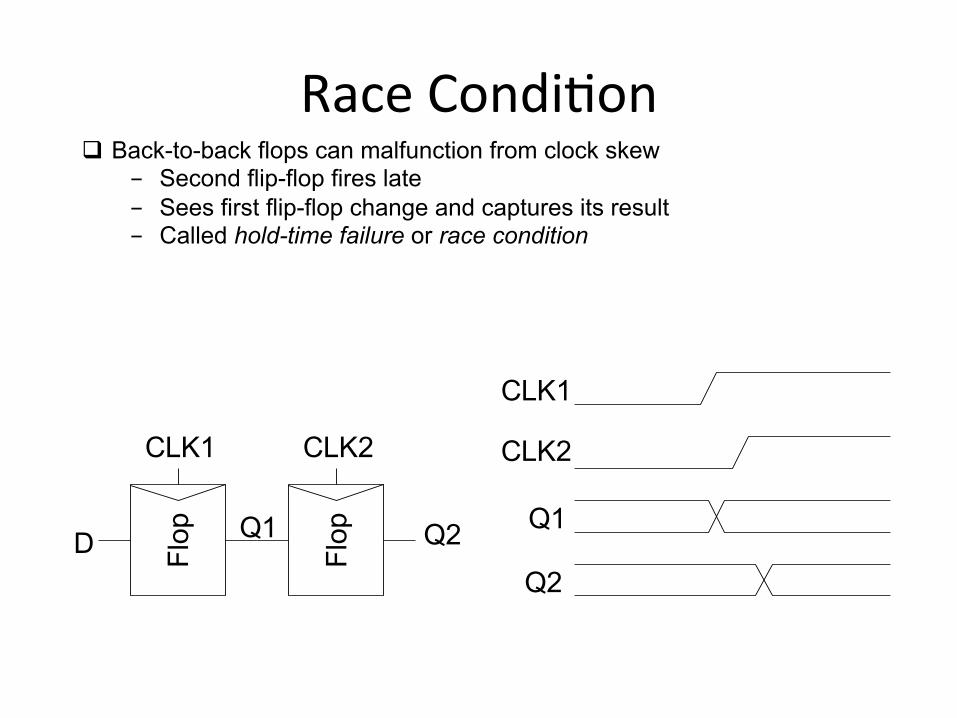
RaceCondi:on
CLK1
D Q1
Flop
Flop
CLK2
Q2
CLK1
CLK2
Q1
Q2
q Back-to-back flops can malfunction from clock skew - Second flip-flop fires late - Sees first flip-flop change and captures its result - Called hold-time failure or race condition

SetupandHoldTime
Time
Volta
ge
Clock Setup Time
Hold Time

Non-overlappingClocksq Non-overlapping clocks can prevent races
- As long as non-overlap exceeds clock skew q We will use them in this class for safe design
- Industry manages skew more carefully instead
φ1
φ1φ1
φ1
φ2
φ2φ2
φ2
φ2
φ1
QMQD

ScanInCell
D Q D Q
phi
phib
scan_i0o1
load
phi_out
phib_out
scan_i0o1_out
load_out
scan_in
chip_in_int
scan_i0o1
phi phib
01 scan_out
scan_out_int
D Qload chip_in
scan_out_int chip_in_int

ScanOutCell
D Q D Q
phi
phib
scan_i0o1
load
phi_out
phib_out
scan_i0o1_out
load_out
scan_in
chip_out
scan_i0o1
phi phib
01 scan_out

ScanIn-OutCell
D Q D Q
phi
phib
scan_i0o1
load
phi_out
phib_out
scan_i0o1_out
load_out
scan_in
chip_out
scan_i0o1
phi phib
01 scan_out
scan_out_int
D Qload chip_in
scan_out_int chip_in_int

GateLayoutq Layout can be very time consuming
- Design gates to fit together nicely - Build a library of standard cells
q Standard cell design methodology - VDD and GND should abut (standard height) - Adjacent gates should satisfy design rules - nMOS at bottom and pMOS at top - All gates include well and substrate contacts

StandardCellsq Uniform cell height q Uniform well height q M1 VDD and GND rails q M2 Access to I/Os q Well / substrate taps q Exploits regularity
CopingWithComplexityq How to design System-on-Chip?
- Many millions (even billions!) of transistors - Tens to hundreds of engineers
q Structured Design q Design Partitioning

StructuredDesignq Hierarchy: Divide and Conquer
- Recursively system into modules q Regularity
- Reuse modules wherever possible - Ex: Standard cell library
q Modularity: well-formed interfaces - Allows modules to be treated as black boxes
q Locality - Physical and temporal

DesignPar::oningq Architecture: User’s perspective, what does it do?
- Instruction set, registers - MIPS, x86, Alpha, PIC, ARM, …
q Microarchitecture - Single cycle, multi-cycle, pipelined, superscalar?
q Logic: how are functional blocks constructed - Ripple carry, carry look-ahead, carry select adders
q Circuit: how are transistors used - Complementary CMOS, pass transistors, domino
q Physical: chip layout - Datapaths, memories, random logic

HDLq Hardware Description Languages
- Widely used in logic design - Verilog and VHDL
q Describe hardware using code - Document logic functions - Simulate logic before building - Synthesize code into gates and layout
• Requires a library of standard cells
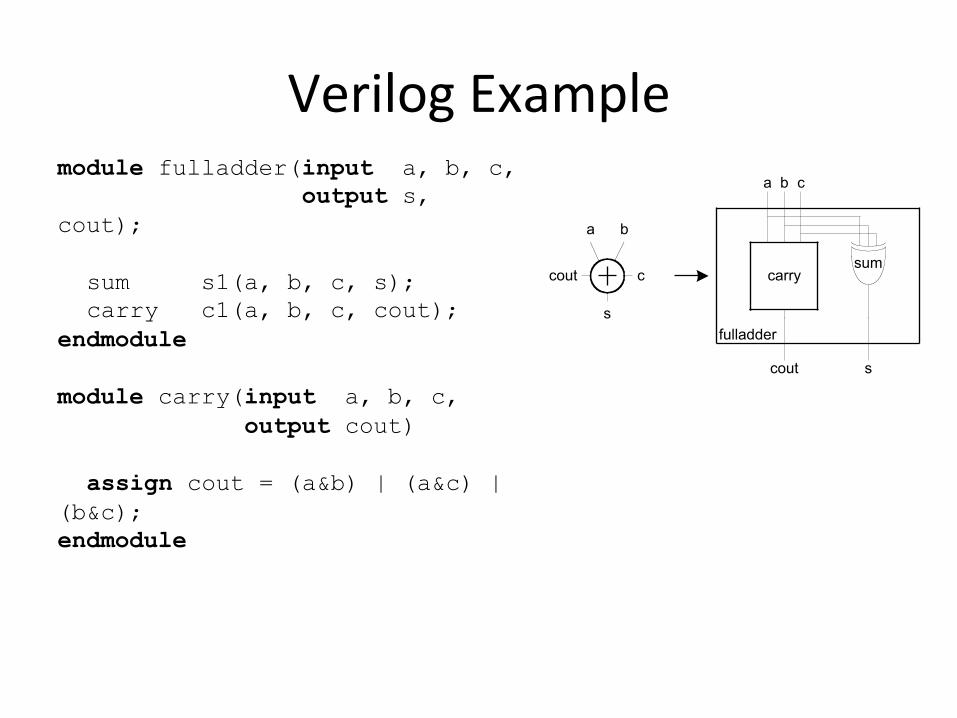
VerilogExamplemodule fulladder(input a, b, c, output s, cout); sum s1(a, b, c, s); carry c1(a, b, c, cout); endmodule module carry(input a, b, c, output cout) assign cout = (a&b) | (a&c) | (b&c); endmodule
a b
c
s
cout carrysum
s
a b c
cout
fulladder

CircuitDesignq How should logic be implemented?
- NANDs and NORs vs. ANDs and ORs? - Fan-in and fan-out? - How wide should transistors be?
q These choices affect speed, area, power q Logic synthesis makes these choices for you
- Good enough for many applications - Hand-crafted circuits are still better

Example:CarryLogic
ab
ac
bc
cout
x
y
z
g1
g2
g3
g4
a b
c
c
a b
b
a
a
b
coutcn
n1 n2
n3
n4
n5 n6
p6p5
p4
p3
p2p1
i1
i3
i2
i4
q assign cout = (a&b) | (a&c) | (b&c);
Transistors? Gate Delays?

GateLevelNetlist
ab
ac
bc
cout
x
y
z
g1
g2
g3
g4
module carry(input a, b, c, output cout) wire x, y, z; and g1(x, a, b); and g2(y, a, c); and g3(z, b, c); or g4(cout, x, y, z);endmodule

TransistorLevelNetlist
a b
c
c
a b
b
a
a
b
coutcn
n1 n2
n3
n4
n5 n6
p6p5
p4
p3
p2p1
i1
i3
i2
i4
module carry(input a, b, c, output cout) wire i1, i2, i3, i4, cn; tranif1 n1(i1, 0, a); tranif1 n2(i1, 0, b); tranif1 n3(cn, i1, c); tranif1 n4(i2, 0, b); tranif1 n5(cn, i2, a); tranif0 p1(i3, 1, a); tranif0 p2(i3, 1, b); tranif0 p3(cn, i3, c); tranif0 p4(i4, 1, b); tranif0 p5(cn, i4, a); tranif1 n6(cout, 0, cn); tranif0 p6(cout, 1, cn);endmodule
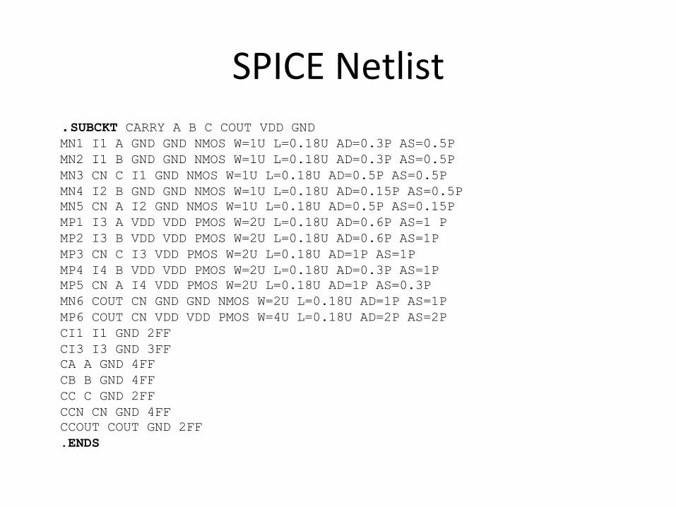
SPICENetlist.SUBCKT CARRY A B C COUT VDD GND MN1 I1 A GND GND NMOS W=1U L=0.18U AD=0.3P AS=0.5P MN2 I1 B GND GND NMOS W=1U L=0.18U AD=0.3P AS=0.5P MN3 CN C I1 GND NMOS W=1U L=0.18U AD=0.5P AS=0.5P MN4 I2 B GND GND NMOS W=1U L=0.18U AD=0.15P AS=0.5P MN5 CN A I2 GND NMOS W=1U L=0.18U AD=0.5P AS=0.15P MP1 I3 A VDD VDD PMOS W=2U L=0.18U AD=0.6P AS=1 P MP2 I3 B VDD VDD PMOS W=2U L=0.18U AD=0.6P AS=1P MP3 CN C I3 VDD PMOS W=2U L=0.18U AD=1P AS=1P MP4 I4 B VDD VDD PMOS W=2U L=0.18U AD=0.3P AS=1P MP5 CN A I4 VDD PMOS W=2U L=0.18U AD=1P AS=0.3P MN6 COUT CN GND GND NMOS W=2U L=0.18U AD=1P AS=1P MP6 COUT CN VDD VDD PMOS W=4U L=0.18U AD=2P AS=2P CI1 I1 GND 2FF CI3 I3 GND 3FF CA A GND 4FF CB B GND 4FF CC C GND 2FF CCN CN GND 4FF CCOUT COUT GND 2FF .ENDS

PhysicalDesignq Floorplan q Standard cells
- Place & route q Datapaths
- Slice planning q Area estimation

MIPSFloorplan
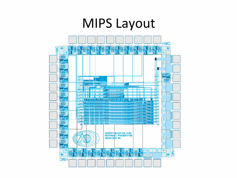
MIPSLayout

SynthesizedControllerq Synthesize HDL into gate-level netlist q Place & Route using standard cell library

DesignVerifica:onq Fabrication is slow & expensive q Debugging chips is very hard
- Limited visibility into operation q Prove design is right before building!
- Logic simulation - Ckt. simulation / formal verification - Layout vs. schematic comparison - Design & electrical rule checks
q Verification is > 50% of effort on most chips!
Specification
ArchitectureDesign
LogicDesign
CircuitDesign
PhysicalDesign
=
=
=
=
Function
Function
Function
FunctionTimingPower

VLSIFlowq Design Compiler (DC) Synopsys tool
DesignCompilerop:mizesdesignstoprovidethesmallestandfastestlogicalrepresenta:onofagivenfunc:on.ItcomprisestoolsthatsynthesizeyourHDLdescrip:onsintoop:mized,technology-dependent,gate-leveldesigns.

Fabrica:on&Packagingq Tapeout final layout q Fabrication
- 6, 8, 12” wafers - Optimized for throughput, - not latency (10 weeks!) - Cut into individual dice
q Packaging - Bond gold wires from die I/O pads to
package

Tes:ngq Test that chip operates
- Design errors - Manufacturing errors
q A single dust particle or wafer defect kills a die - Yields from 90% to < 10% - Depends on die size, maturity of process - Test each part before shipping to customer

MIPSR3000Processorq 32-bit 2nd generation commercial processor (1988) q Led by John Hennessy (Stanford, MIPS Founder) q 32-64 KB Caches q 1.2 µm process q 111K Transistors q Up to 12-40 MHz q 66 mm2 die q 145 I/O Pins q VDD = 5 V q 4 Watts q SGI Workstations
http://gecko54000.free.fr/?documentations=1988_MIPS_R3000

TransistorasSwitches
gs
d
g = 0
s
d
g = 1
s
d
gs
d
s
d
s
d
nMOS
pMOS
OFF ON
ON OFF
q We can view MOS transistors as electrically controlled switches q Voltage at gate controls path from source to drain

CMOSInverter
VDD
A Y
GND
A Y
0 1
1 0
A Y

CMOSNANDGate
A B Y
0 0 1
0 1 1
1 0 1
1 1 0 A
B
Y

CMOSNORGate
A B Y
0 0 1
0 1 0
1 0 0
1 1 0
A
BY

ComplementaryCMOSq Complementary CMOS logic gates
- nMOS pull-down network - pMOS pull-up network - a.k.a. static CMOS pMOS
pull-upnetwork
outputinputs
nMOSpull-downnetworkPull-up OFF Pull-up ON
Pull-down OFF Z (float) 1
Pull-down ON 0 X (crowbar)

SeriesandParallelq nMOS: 1 = ON q pMOS: 0 = ON q Series: both must be ON q Parallel: either can be ON (a)
a
b
a
b
g1
g2
0
0
a
b
0
1
a
b
1
0
a
b
1
1
OFF OFF OFF ON
(b)
a
b
a
b
g1
g2
0
0
a
b
0
1
a
b
1
0
a
b
1
1
ON OFF OFF OFF
(c)
a
b
a
b
g1 g2 0 0
OFF ON ON ON
(d) ON ON ON OFF
a
b
0
a
b
1
a
b
11 0 1
a
b
0 0
a
b
0
a
b
1
a
b
11 0 1
a
b
g1 g2

Conduc:onComplementq Complementary CMOS gates always produce 0 or 1 q Ex: NAND gate
- Series nMOS: Y=0 when both inputs are 1 - Thus Y=1 when either input is 0 - Requires parallel pMOS
q Rule of Conduction Complements - Pull-up network is complement of pull-down - Parallel -> series, series -> parallel
A
B
Y
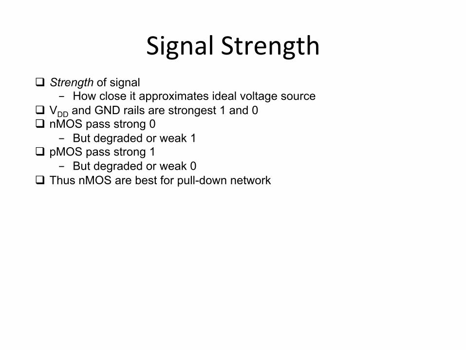
SignalStrengthq Strength of signal
- How close it approximates ideal voltage source q VDD and GND rails are strongest 1 and 0 q nMOS pass strong 0
- But degraded or weak 1 q pMOS pass strong 1
- But degraded or weak 0 q Thus nMOS are best for pull-down network

PassTransistorsq Transistors can be used as switches
g = 0s d
g = 1s d
0 strong 0Input Output
1 degraded 1
g = 0s d
g = 1s d
0 degraded 0Input Output
strong 1
g = 1
g = 1
g = 0
g = 01
g
s d
g
s d

TransmissionGatesq Pass transistors produce degraded outputs q Transmission gates pass both 0 and 1 well
g = 0, gb = 1a b
g = 1, gb = 0a b
0 strong 0
Input Output
1 strong 1
g
gb
a b
a bg
gb
a bg
gb
a bg
gb
g = 1, gb = 0
g = 1, gb = 0

Tristatesq Tristate buffer produces Z when not enabled
EN A Y 0 0 Z 0 1 Z 1 0 0 1 1 1
A Y
EN
A Y
EN
EN

Non-restoringTristateq Transmission gate acts as tristate buffer
- Only two transistors - But non-restoring
• Noise on A is passed on to Y
A Y
EN
EN
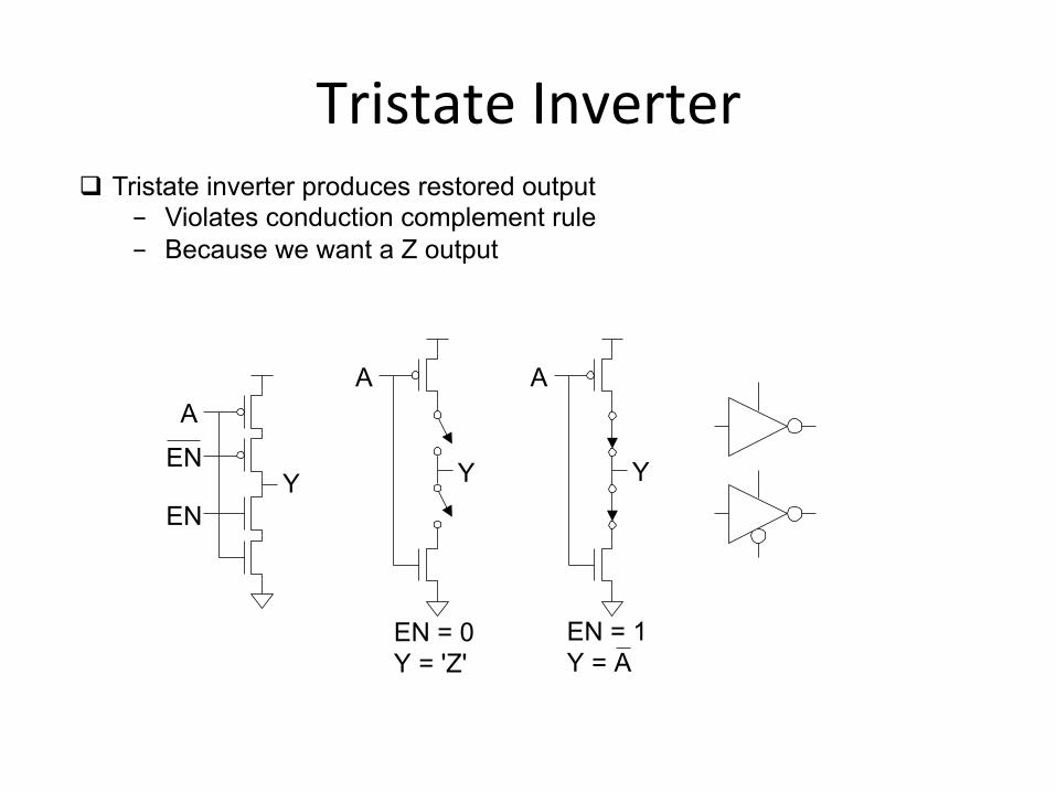
TristateInverterq Tristate inverter produces restored output
- Violates conduction complement rule - Because we want a Z output
A
YEN
A
Y
EN = 0Y = 'Z'
Y
EN = 1Y = A
A
EN
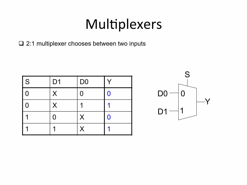
Mul:plexersq 2:1 multiplexer chooses between two inputs
S D1 D0 Y
0 X 0 0
0 X 1 1
1 0 X 0
1 1 X 1
0
1
S
D0
D1Y
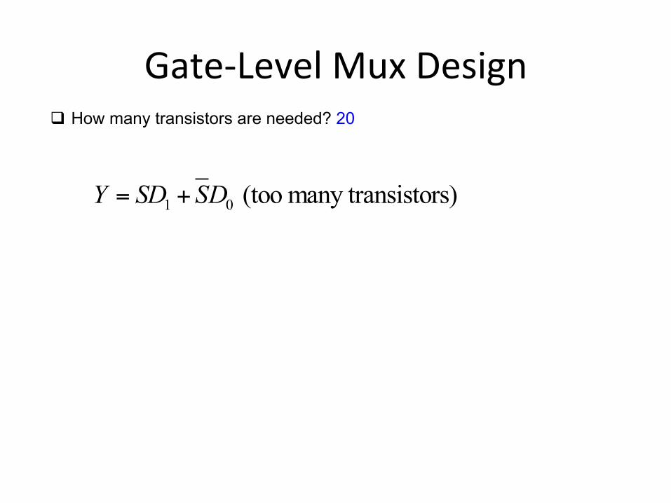
Gate-LevelMuxDesignq How many transistors are needed? 20
1 0 (too many transistors)Y SD SD= +