ECE Department: University of Massachusetts, Amherst ECE 354 Lab 5: Data Compression.
34
ECE Department: University of Massachusetts, Amherst ECE 354 Lab 5: Data Compression
-
Upload
phillip-melton -
Category
Documents
-
view
217 -
download
3
Transcript of ECE Department: University of Massachusetts, Amherst ECE 354 Lab 5: Data Compression.

ECE Department: University of Massachusetts, Amherst
ECE 354
Lab 5: Data Compression

2ECE 354
In this lab, you will…
Reuse Lab 4 and add additional components
Write both Verilog modules and C code• Use custom Verilog modules along side the NIOS core• Use C to interact with external Verilog modules

3ECE 354
System Diagram
Master Board Slave Board
CommandCommand
Encoded Picture DataEncoded Picture Data
MonitorMonitor
CameraCamera
MonitorMonitor
RLE Encoder(Hardware)
RLE Encoder(Hardware)
NIOSSoftware
NIOSSoftware
RLE Decoder(Software)
RLE Decoder(Software)
BMP bit stream Encoded data
NIOSSoftware
Serial Port
VGA PortVGA Port

4ECE 354
Overview
Implement new features by adding Verilog files into a current system.• Buffer Modules (Input & Output)• RLE Compression Module
Add SOPC components to interface with the new module• Output PIO• Input PIO• Control PIOs
Write software to control and implement module usage

5ECE 354
System Overview

6ECE 354
RLE Hardware Block Structure and Integration
NIOS coreNIOS core
FIFO_sendFIFO_send FIFO_recvFIFO_recvRLE UnitRLE Unit
OD
AT
A_P
IO[7
:0]
FIF
O_I
N_W
RIT
E_R
EQ
_PIO
FIF
O_I
N_F
ULL
_PIO
IDA
TA
_PIO
[23:
0]
RE
SU
LT_R
EA
DY
_PIO
FIF
O_O
UT
_RE
AD
_RE
Q_P
IO
RLE
_FLU
SH
_PIO
FIFO_IN_ODATA[7:0]
FIFO_IN_READ_REQ
FIFO_IN_EMPTY
RLE_OUT[23:0]
RLE_DONE
FIFO_OUT_FULL

7ECE 354
FIFO Buffer
Saves data based on specified clock Holds values in registers until requested Outputs data in a specified way
• Same order in which it came into the buffer• First In the buffer, first to come out (FIFO)
• Sends data only when requested by a signal Used due to asynchronous signals and data sent from the software

8ECE 354
Run Length Encoder
Takes data stream and records how many bits are the same Input – 8 Bit data stream segments Output – 24 Bit Data How is more data bits compression?
• First bit – ID Bit (0 or 1)• 23 bits – Number of 0 or 1s
• More of same value in sequence, more data is saved• Worse Case - Interchanging data (01010101.....)• Use VGA data (1bit data) for compression and data exchange.
• More likely to get same value
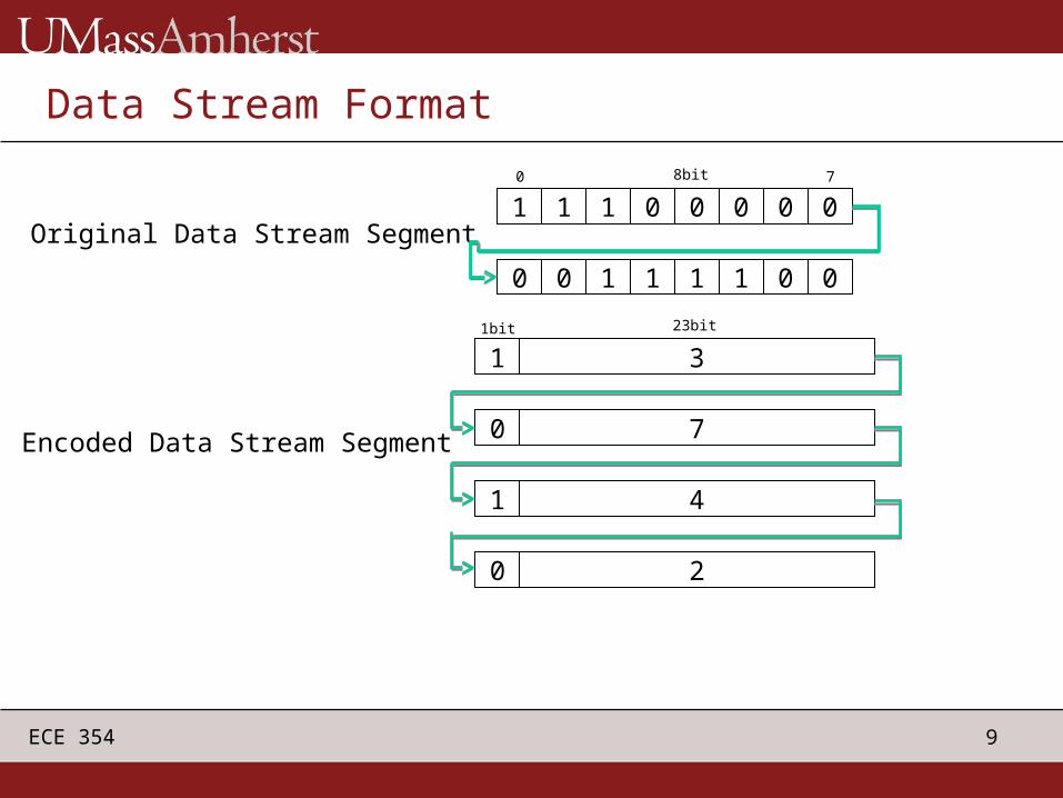
9ECE 354
Data Stream Format
1 1 1 0 0 0 0 0
1 3
0 7
23bit1bit
Original Data Stream Segment
Encoded Data Stream Segment
8bit
0 0 1 1 1 1 0 0
1 4
0 2
0 7

10ECE 354
Signals in Block Structure (To be added in SOPC)
ODATA_PIO[7:0]• Output ports to send original bit-stream. 8-bit segment is sent at the same time
FIFO_IN_WRITE_REQ_PIO• Assert write request signal for FIFO. FIFO stores input data when this signal is asserted
FIFO_IN_FULL_PIO• Indicate FIFO is full. Sending picture data stream should wait until this signal is de-asserted
IDATA_PIO[23:0]• Input ports to receive the encoded data• 1 bit for bit ID, 23bits for representing number of bits.• RLE can be implemented with smaller number of bits. However, in this lab, we use big enough bits to
represent 640*480 picture RESULT_READY_PIO
• Notify that there is an encoded data segment in the FIFO. Inverse of FIFO empty signal is used for this signal
FIFO_OUT_READ_REQ_PIO• Assert Read request signal for FIFO. FIFO produces next data from the buffer when this signal is
asserted RLE_FLUSH_PIO
• Notify the end of the bit-stream. RLE produces a new encoded data segment immediately with current counting value

11ECE 354
Signals in Block Structure (2)
FIFO_IN_READ_REQ• Assert read request signal for FIFO
FIFO_IN_EMPTY• Notify FIFO is empty. Therefore, RLE unit should wait until new data is available
RLE_OUT• Pass the encoded data to the FIFO
RLE_DONE• Notify encoding process is done, which means a new encoded data segment is
ready. It is also used as a write assert signal for the FIFO FIFO_OUT_FULL
• Notify FIFO is full. Therefore RLE unit should wait until this signal is de-asserted FIFO_IN_ODATA[7:0]
• Provide a next bit-stream segment to RLE unit when FIFO_IN_READ_REQ is asserted

12ECE 354
Process for Lab5
Take your LAB4 Create additional PIO with SOPC builder for your new hardware
• Check module system_0 in system_0.v• Make sure new PIO ports are generated
Add your rle_enc.v and rle_fifo_8_24.v into your quartus project Modify DE2_NET.v
• Instantiate your RLE unit and two FIFO modules• Connect your hardware and SOPC core (system_0 u0)
• You need to write additional parameters for system_0 u0 to connect them with PIO

13ECE 354
Contd.,
Full source code for 8 bit and 24 bit FIFO will be provided• rle_fifo_8_24.v
Partial code for RLE unit will be provided• Code for state transition will be given to you• You will implement some parts that commented out • You can modify if you have better idea
Run-length Encoding• rle_enc.v
Top-level module• DE2_NET.v• You will need to modify to connect your new hardware

14ECE 354
RLE completion and Simulation
Complete the rle_enc.v• Simulate it if it is needed (optional)
Make sure your RLE module and file have the same name Set RLE module as your Top-level design
• Open verilog file that has RLE module• Menu->Project->Set as top-level entity
You need to generate input stimulus for RLE (optional to check RLE)• Tutorial : http://www.ecs.umass.edu/ece/engin112/labs/Quartus-tutorial_sc
hematic.pdf
Open NIOS IDE• Write code to control your hardware• Write a function for decoding
15ECE 354
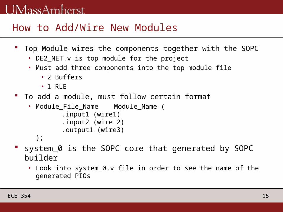
How to Add/Wire New Modules
Top Module wires the components together with the SOPC• DE2_NET.v is top module for the project• Must add three components into the top module file
• 2 Buffers• 1 RLE
To add a module, must follow certain format• Module_File_Name Module_Name (
.input1 (wire1)
.input2 (wire 2)
.output1 (wire3));
system_0 is the SOPC core that generated by SOPC builder• Look into system_0.v file in order to see the name of the generated PIOs
16ECE 354
Verilog Simulation
A good debugging tool• If your hardware doesn’t work correctly• Sometimes it is hard to debug with LEDs and switches
Verilog language has ambiguity for simulation• E.g) Race Condition• Need to keep some guidelines to get correct result
Quartus has simulation capability

17ECE 354
Race Condition
Produces different simulation result from real hardware
Keeping verilog design guideline is important
always @(posedge clk) a = b;always @(posedge clk) b = c;
Which statement will be executed first?
An Example

18ECE 354
Shift-Register in Verilog
Incorrect implementationalways @(posedge clk) begin
shift_reg[2] = shift_reg[3];shift_reg[1] = shift_reg[2];shift_reg[0] = shift_reg[1];
end
* ‘=‘ : Blocking Assignment* Value in shift_reg[3] will beassigned to shift_reg[0] directly
Correct implementationalways @(posedge clk) begin
shift_reg[2] <= shift_reg[3];shift_reg[1] <= shift_reg[2];shift_reg[0] <= shift_reg[1];
End
* ‘<=‘ : Non-Blocking Assignment* Updating will happen aftercapturing all right-side register
values

19ECE 354
Important Design Guideline for LAB5
Do not mix BA and NBA in the same always block Use BA for combinational circuit in given design
• State transition Use NBA for sequential circuit in given design
• Updating registers

20ECE 354
Software Design
Use Altera functions to send/receive data• inport() / outport()• (IOWR/IORD)_ALTERA_AVALON_PIO_DATA()
Send data to be compressed• while(buffer_not_full){
outport(data_pio_base, data);.....;
} Receive data from compression
• if(buffer_not_empty){data = inport(dataout_pio_base);....;
}

21ECE 354
Software Design
Software (Master) must be able to decompress data• Relatively easy
• Data tells you what to write• Example: (10000000 00000000 00000111)
• First Value = 1• Second Value = 7• Write 1, 7 times• Output: 1111111

22ECE 354
Tips
Go through the videos posted in the class website before starting the Lab-5.
Open SOPC builder in classic mode when adding the PIO to the system Compressed Data is variable length for every picture
• Data could be compressed smaller, or expanded into larger data• Assume data can be larger than picture data and Make compression data
array to be bigger• Make sure Master knows how big the data is
• Sequenced numbered packets• End Packet• Information Packet
Appendix attached at the end of the presentation describes the different signals used in FIFO buffer and RLE.

23ECE 354
Summary
To implement hardware and software for RLE• Encoding is done by Hardware
• GPIO is used• Read/Write data from/to hardware is done by using ALTERA API
• Decoding is done by Software The RLE implementation is added to Lab4
• You send encoded picture data to the other board• The data stream has variable length• The data stream is decoded by software on receiving board• Display the images before compression in slave board and the decoded
image from the master.

24ECE 354
Comments and/or Questions

ECE Department: University of Massachusetts, Amherst
AppendixSignals and their Description

26ECE 354
RLE Interface - Input
input clk,rst• clk and reset
input recv_ready• Connected with (!fifo_empty) of input side FIFO
input send_ready• Connected with (!fifo_full) of output side FIFO
input [7:0] in_data• Input data from input side FIFO• 8 bit segment of original bit stream
input end_of_stream• Indicate the end of bit stream• Request flushing out the last segment

27ECE 354
RLE Interface - Output
output [23:0] out_data• Output data to output side FIFO• [23] has bit ID, [22:0] has bit counting value
output rd_req• Read request for input side FIFO
output wr_req• Write request for output side FIFO

28ECE 354
RLE Internal Signals
reg rd_reg• connected to rd_req;
reg wr_reg• Connected to wr_req;
reg [22:0] bit_count• Stores number of same consecutive bit in bit stream• value_type represent bit ID
reg value_type• Bit ID
29ECE 354
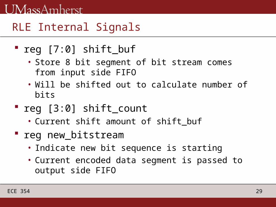
RLE Internal Signals
reg [7:0] shift_buf• Store 8 bit segment of bit stream comes from input side
FIFO• Will be shifted out to calculate number of bits
reg [3:0] shift_count• Current shift amount of shift_buf
reg new_bitstream• Indicate new bit sequence is starting• Current encoded data segment is passed to output side
FIFO

30ECE 354
RLE Internal Signals
reg [3:0] state• Represent State.• There are 9 states in total
reg [3:0] next_state• Represent Next state

31ECE 354
READ_INPUTshift_buf = in_data
WAIT_INPUTrd_reg = 0
REQUEST_INPUTrd_reg = 1
shift_count = 0
COUNT_BITSIncrease bit_count
Set/resetnew_bitstream
SHIFT_BITSShift sift_buf
Increaseshift_count
Lookupnew_bitstream
COUNT_DONEwr_reg = 1
WAIT_OUTPUTwr_reg = 0
RESET_COUNTbit_count = 0
INITbit_count = 0shift_buf = 0rd_reg = 0
wr_req_reg = 0new_bitstream = 1
!recv_read
!recv_read&end_of_stream&bit_count != 0
new_bitstream
shift_count == 7
send_ready
end_of_stream

32ECE 354
RLE State in detail INIT
• Initialize registers REQUEST_INPUT
• Assert rd_req signal to FIFO by setting rd_reg• FIFO takes rd_req signal at next clock
WAIT_INPUT• 1 cycle stall is needed• De-assert rd_req by setting rd_reg
READ_INPUT• FIFO provides valid data after taking rd_req• shift_buf stores 8 bit input data

33ECE 354
RLE State in detail
COUNT_BITS• Count number of consecutive bits in shift_buf• If new type of bit starts, store bit ID in value_type register• If current value_type and shift_buf[0] is not matched, notify current encoding
is completed and new encoding will be started SHIFT_BITS
• Right shift the shift_buf• Increase shift_count• Look up new_bitstream
COUNT_DONE• Assert wr_req by setting wr_reg• FIFO will take wr_req signal in next clock cycle

34ECE 354
RLE State in detail
WAIT_OUTPUT• 1 cycle stall is needed• De-assert wr_req by setting wr_reg
RESET_COUNT• Reset bit counting register after passing encoded data to output side FIFO