ECE 525 Digital Circuit Design I CH5: CMOS...
21
ECE 525 – Digital Circuit Design I CH5: CMOS Power Andrew Chuinard February 21, 2011
Transcript of ECE 525 Digital Circuit Design I CH5: CMOS...

ECE 525 – Digital Circuit Design I
CH5: CMOS Power
Andrew Chuinard
February 21, 2011

2
Presentation Overview Introduction
CMOS Dissipation
Static Dissipation
Dissipation Sources
Subthreshold Leakage, Gate Leakage
Other Sources
Power Gating
Dynamic Dissipation
Dissipation Sources
Switching loss
Glitches
Short-Circuit Current
Clock Gating
Voltage Voltage Domains
Dynamic Voltage Scaling (DVS)
Energy-Delay Optimization

3
Introduction
)()()( tVtItP
T
avg dttPT
P0
)(1
dttPE
T
)(0
Fundamental Equations
Instantaneous Power
Energy Consumed (or supplied)
Average Power

4
Introduction
Sources of power dissipation
Static dissipation
Subthreshold leakage (OFF transistors)
Gate leakage through dielectric
Junction leakage
Dynamic dissipation
Charging and discharging load capacitance
Short-circuit current when nMOS and pMOS are partially
ON

5
Introduction

6
Introduction

7
Static Dissipation: Subthreshold Leakage
Definition: The current
that flows when the
transistor is supposed
to be OFF
S
V
offsub
sbVkDDVdsVgs
II
)(
10
(Equation 5.19)

8
Static Dissipation: Gate Leakage
Caused by carriers
tunneling through gate
dielectric
Case (a): N2 OFF
N1 has a Vgs voltage
equal to VDD, the
maximum possible.
Case (b): N1 OFF
N2 has a Vgs of Vt,
negligible compared to
case (a)

9
Static Dissipation: Other Sources
Junction Leakage: Caused by source or drain
diffusion region at a different potential than
substrate
Contention Current: Caused by circuits that require
static current draw. For CMOS circuits this does
not apply
10
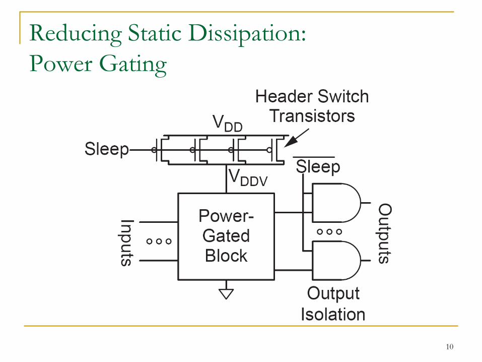
Reducing Static Dissipation:
Power Gating

11
Reducing Static Dissipation:
Multiple Threshold Voltages
Lower threshold voltage increases leakage
Increase threshold voltage on non-critical
performance paths using high Vt transistors
Advantage: Optimizes leakage losses
Disadvantage: Adds complication to the CMOS
fabrication process
Dynamically change Vt by reverse biasing
body (Variable threshold CMOS: VTCMOS)

12
Dynamic Dissipation
In CMOS circuits, dynamic power dissipation
comes from:
Switching loss
Short circuit current
Conduction losses when PMOS and NMOS are partially
ON
swDDswitching fCVP 2
13
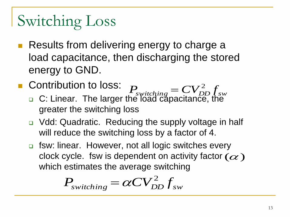
Switching Loss
Results from delivering energy to charge a
load capacitance, then discharging the stored
energy to GND.
Contribution to loss:
C: Linear. The larger the load capacitance, the
greater the switching loss
Vdd: Quadratic. Reducing the supply voltage in half
will reduce the switching loss by a factor of 4.
fsw: linear. However, not all logic switches every
clock cycle. fsw is dependent on activity factor
which estimates the average switching
swDDswitching fCVP 2
swDDswitching fCVP 2
)(

14
Switching Loss (Continued)
Contributions to loss:
Glitches
With finite propagation
delay, erroneous
switching can occur
when inputs do not
have the same arrival
time
With significant
“glitching”, the activity
factor can be greater
than 1.

15
Short Circuit Current
•Power dissipation when both the PMOS and NMOS transistor are
partially ON
•Typically 10% or less of dissipation
•Reduction Methods
•Large load capacitance
•Reduces the change in output voltage during input transition
•Larger Vt
•As Vt increases with respect to Vdd, the time that both the
NMOS and PMOS can be on simultaneously is reduced

16
Dynamic Dissipation: Loss Reduction
•Clock Gating
•Add additional
logic to disable
clock
•Removes
unnecessary
switching loss
from idle circuits

17
Dynamic Dissipation: Loss Reduction•Voltage Domains
•Use of separate supply voltages optimized
for circuit needs
•Advantage: Power loss is reduced by the
reduction in voltage squared
•Disadvantage: Careful circuit design is
required to ensure correct interaction
between circuits
•i.e. Higher voltage circuit can drive low
voltage circuit, but low voltage may not
meet threshold requirements
•Can implement a level shift circuit at
voltage transition, but this requires both
supply rails available

18
Dynamic Dissipation: Loss Reduction•Dynamic Voltage/Frequency Scaling
(DVFS)
•Optimize supply voltage in real time for
different operating conditions
•Advantage: Reduces power dissipation
during operation that does not require
maximum performance
•Disadvantage: Additional
hardware/control mechanism required.
Continuously adjustable supply would
be costly

19
Energy-Delay Optimization Question: What is the best choice of Vdd & Vt?
Minimum Energy?
For true minimum energy, delay approaches infinity (no switching loss)
Minimum Delay?
Switching loss dominates
Several conflicting design parameters
Vdd-Vt decreases
Current reduces exponentially
Delay increases exponentially
Vdd reduction
Leakage current reduces slowly with Vdd reduction
Leakage energy increases exponentially because gate is slower and leaks for a longer time
Switching loss reduced quadratically

20
Energy-Delay Optimization

21
Sources
CMOS VLSI Design, Fourth Edition: Weste &
Harris
http://web.cecs.pdx.edu/~chiang/ECE_425_5
25_Winter_2011/