
Management of DCIS Fei-Fei Liu Radiation Oncologist/Senior Scientist.

Week 5. Hardware: Sensor Mote Architecture and Design
From Dr. Fei Hu's written textbook
Outline:- analog sensors- microcontroller- memory- RF (Radio Frequency) communication unit- Battery - put everything together into an intelligent sensor mote system.
2.1 Components of a Sensor Mote [Jason03]
2.1.1 Sensors
1 | P a g e
Remember: A mote (i.e., a WSN sensor node) is a typical embedded system from computer engineering design viewpoint. As we know, any embedded system needs a microprocessor (also called CPU or microcontroller) to control all other chips. But a mote needs to achieve wireless networking with other motes, its CPU needs to interface to RF transceiver. How do we interface CPU and radio chips in a fast, low-energy way is a challenging issue.
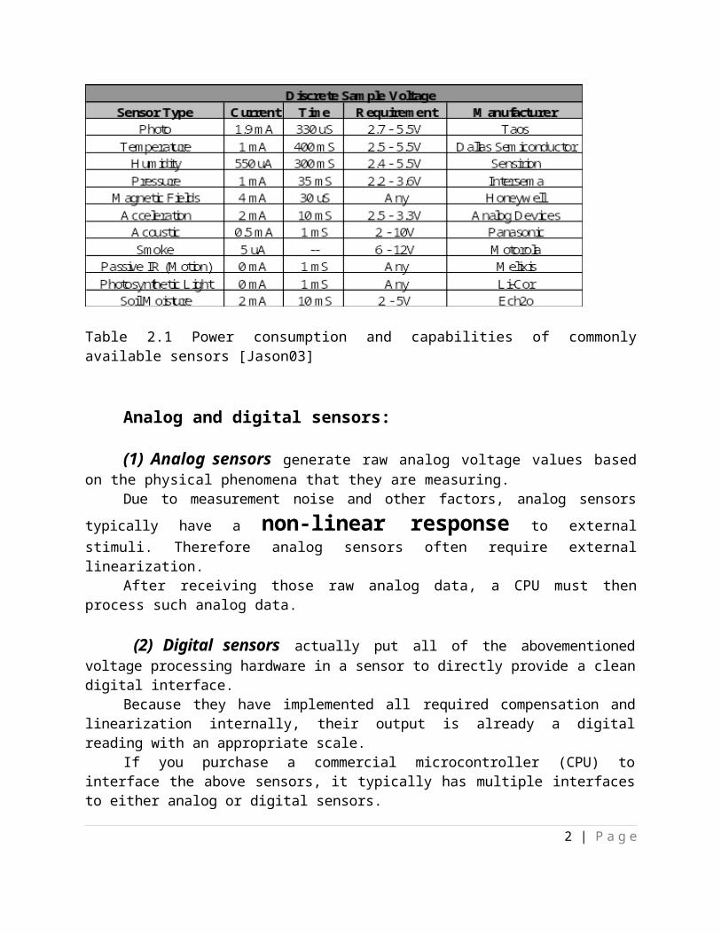
Table 2.1 Power consumption and capabilities of commonly available sensors [Jason03]
Analog and digital sensors:
(1) Analog sensors generate raw analog voltage values based on the physical phenomena that they are measuring.
Due to measurement noise and other factors, analog sensors typically have a non-linear response to external stimuli. Therefore analog sensors often require external linearization.
After receiving those raw analog data, a CPU must then process such analog data.
(2) Digital sensors actually put all of the abovementioned voltage processing hardware in a sensor to directly provide a clean digital interface.
Because they have implemented all required compensation and linearization internally, their output is already a digital reading with an appropriate scale.
If you purchase a commercial microcontroller (CPU) to interface the above sensors, it typically has multiple interfaces to either analog or digital sensors.
Although most sensors have the capability of producing thousands of samples per second, in practice we are only interested in a few samples per minute. Such a low duty cycle can greatly save energy.
It is important to turn on/off a sensor as quickly as it can in order to save energy. For example, if a sensor takes 100 ms to turn on and reads a sample, assume the sample reading consumes just 1 mA at 3 V, it will cost 300 µJ (=V.I.T) in total to get a sample. This is the same amount of energy as a sensor that consumes 1000 mA of current at 3 V but takes just 100 us to turn on and read a sample.
It needs some extra circuitry if a sensor’s voltage requirements do not match the capabilities of the system. For instance, some sensors require +/- 6 V. If a sensor just uses AA or lithium batteries, we need special voltage converters and regulators in order to use this sensor. The power consumption and turn-on times of converters and regulators’ circuitry must be included in the total energy budget for the sensor.
2.1.2 Microprocessor
2 | P a g e
Today, almost all analog sensors convert environmental parameters into a readable low voltage level. How to interpret those voltage levels from event detection perspective is a difficult issue. Moreover, we need to capture such a weak current and use ADC to get digital signals. During the ADC the noise from hardware and environments should be removed.

microcontrollers (i.e. tiny CPUs, also called microprocessors or processors), When selecting a commercial microcontroller family for a WSN application, we need to
consider some of the key requirements including energy consumption, voltage requirements, cost, support for peripherals, and the number of external components required.
The power consumption when a CPU is in sleep mode is an important performance metric. In sleep mode the CPU stops execution except that it maintains basic memory activities and time synchronization in case later on it needs to timely wake-up. The current consumption in sleep mode varies between 1 µA and 50 µA across CPU families. Since the CPU is expected to be idle 99.9% of the time, such a 50x µA difference can have a more significant impact on mote performance than mA differences in peak power consumption.
Besides the energy consumption level in sleep mode, we also care about how much time the operation of entering / exiting sleep mode takes. Such a transition time (entering sleep / wake-up time) could take 6 µs ~ 10 ms. The wake-up delay is used to start and stabilize system clocks. The faster a CPU can enter or leave the sleep mode, the more energy a mote can save. As a matter of fact, by quickly wake-up, we can put a mote into sleep mode even at a very short period of inactivity. For example, during a message transmission, the controller can enter the sleep mode between each bit of transmission. Active current consumption of the controller is reduced by longer sleep time.
CPU performance also depends on the operating voltage range. Traditional WSN microcontrollers operate between 2.7V and 3.3 V. Recently, new generations of low-power CPUs can even operate on 1.8 V. WSN applications need a wide voltage tolerance.
In a WSN, the CPU needs to execute the wireless communication protocols and perform local data processing. Those operations do not need a high-speed CPU. That’s why most of today’s WSN CPUs have a speed of less than 4M Hz.
Some WSN CPUs can dynamically change the operating frequency. CMOS power consumption obeys the equation P=CV2F. Therefore, higher CPU frequency brings more power consumption. But the COU execution time is inversely proportional to frequency. That is, higher frequency makes a program run faster, which also saves energy. Therefore, it is hard to say that the system energy will change a lot by increasing or reducing CPU frequency.
Table 2.2 lists some important features to be considered when selecting a CPU, such as power, memory size, fast reprogrammability, A/D channels, and operating supply. It compares some suitable CPUs in different motes on the market. Typically Atmel AT90LS8535 offers a good performance in most WSN applications.
3 | P a g e

Table 2.2 Comparison of Microprocessors [Seth00]
A CPU design example: SNAP/LE [Virantha04]
a low-energy mote processor called SNAP/LE (Sensor Network Asynchronous Processor/Low Energy), optimized for data monitoring operations in WSNs.
A dominant feature of SNAP/LE is to use asynchronous circuits, which results in automatic, fine-grained power management, which can be seen from the following fact: when a circuit does not perform a particular operation, it won’t have any switching activity. Asynchronous circuits also remove glitches / switching hazards in the CPU, which avoids another source of energy waste.
Another interesting feature of SNAP/LE is that its hardware directly supports event execution, which means that we don’t need an operating system! No OS reduces static and dynamic instruction counts. It also simplifies CPU design since we don’t need to worry about precise exceptions and virtual memory translation.
4 | P a g e
Note that the above table does not intend to list all advanced CPUs used in different embedded systems. Instead, it only lists some popular microcontrollers that may be suitable to small, low-power, low-cost motes. In some products, the microcontrollers are integrated with different memories (such as flash, ROM, etc.).

Traditional mote CPU designs mostly adopt a commodity off-the-shelf (COTS) microcontroller such as Berkeley motes’ Atmel Mega128L [Atmel08]. SNAP/LE doesn’t use commercial CPU, instead, it is a processor designed specifically for WSNs. It not only meets the computational demands of a WSN node, but also consumes much less energy than other CPUs.
SNAP/LE aims to design a CPU with all the following features:
(1) A simple programming model: A good CPU design should allow easy programming.
(2) Lower-power sleep mode: As we mentioned before, sensors remain in sleep status during most of the time.
(3) Low-overhead wakeup mechanism: SNAP/LE aims to achieve around 10ns of transition time, which is much less than an event handling time (a few ms).
(4) Low power consumption while awake: Besides keeping a low power consumption during sleep status, SNAP/LE uses a 16-bit data path. Its instructions can be one or two 16-bit words long
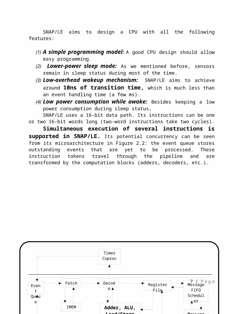
(two-word instructions take two cycles). Simultaneous execution of several instructions is supported in
SNAP/LE. Its potential concurrency can be seen from its microarchitecture in Figure 2.2: the event queue stores outstanding events that are yet to be processed. These instruction tokens travel through the pipeline and are transformed by the computation blocks (adders, decoders, etc.).
5 | P a g e
Good Idea
Customized VLSI vs. COTS design: It is hard to say which one is the dump winner. Typically, from time and complexity viewpoint, most researchers choose to use COTS since so many different companies are providing high-performance, low-cost chips to assemble a mote. However, from cost and performance viewpoint, customized VLSI design is final solution since you could minimize chip size and achieve the best speed/energy performance. Later on, we will cover Spec [Jason03]. Like SNAP/LE, it is also a customized design.

Event Queu
e
Fetch
Timer Coproc.
Adder, ALU, Load/Store Unit,
Jump/Branch, Shifter
Register File
IMEM
Decode Message FIFO
Scheduler
Message Coproc.
DMEM
Figure 2.2 - Microarchitecture of SNAP/LE showing major units. [Virantha04]
SNAP/LE CPU core includes an important component, i.e., the event queue. It works with the instruction fetch unit to form a hardware implementation of a FIFO task scheduler. The scheduler first executes the boot code. When the scheduler reaches “done” instruction, which is also the last instruction in the boot code, it will stop fetching instructions and wait for an event token to appear at the head of the event queue.
Each event token tells what event has occurred. Event tokens are inserted into the event queue by two components: (1) the timer coprocessor when a timeout finishes; (2) the message coprocessor when data arrives from the sensor node’s radio or from one of its sensors.
SNAP/LE has a “deep sleep” state. It takes only 10’s ns for its CPU to wake up from this sleep state. It thus saves energy through “deep sleep” and the low wake-up latency. This feature is not seen in conventional WSN CPUs: most of them have several “sleep” states. For instance, they may have “deeper” sleep state that consumes less power, but requires more time to wake up than a “lighter” sleep state. The Atmel microcontrollers, for example, have six sleep states [26].
6 | P a g e
As we can see from Figure 2.2, SNAP/LE CPU has the following hardware units: an adder, a logic unit, load-store units, a timer unit for interfacing with the timer coprocessor, a jump/branch unit, a linear-feedback shift register (for pseudo-random number generation), and a shifter. The most commonly-used units (such as the adder, the logic unit, the load-store, etc.) are placed on the fast busses and the rest on the slow busses. All of the function units were designed with minimal pipelining in order to limit SNAP/LE’s power consumption while awake.
2.1.3 MemoryAfter we discussed CPU, we move to another important mote component – memory.
Generally WSN motes only require small amounts of storage and program memory. This is because sensor data only stays in local sensor for a short time and then are transmitted through the network to the base station.
Today many flash-based CPUs have an on-chip storage that is typically less than 128K. Such on-chip storage can be used as both program memory and as temporary data storage. WSN CPUs also have a data RAM (between 128 and 32KB) that can be used for program execution.
Let’s take a look at the differences between flash memory and SRAM (static random access memory):
(1) Flash technology has higher density than SRAM. For instance, flash memory could have a storage density of 150 KB per square millimeter in a .25 micron process [AMD03]. While Intel’s recent SRAM density record is 60 KB per square millimeter using a 90 nm process [Intel02].
(2) From energy consumption viewpoint, flash is a persistent storage technology that requires no energy to maintain data. However, SRAM requires more energy to retain data over time, but does not require as much energy for the initial storage operation.
(3) From time viewpoint, a flash write operation requires 4 µs to complete compared to .07 µs for SRAM – both consuming 15 mA.
Therefore, if we need to store data for long periods of time, it is more efficient to use flash instead of SRAM.
2.1.4 Radios
Now let’s discuss another important hardware component in a mote: radio transceiver. First, let’s remember a few facts on motes’ low-power, short range transceivers:
(1) It consumes around 15 ~ 300 milliwatts of power during sending and receiving. (2) It needs approximately the same amount of energy when in receive or transmit mode. (3) As long as the radio is on, whether or not it is receiving actual data, the
energy is consumed. (4) Lots of energy is consumed in receiving packets. The actual power emitted out of the
7 | P a g e

antenna (when sending data) only accounts for a small fraction of the transceiver’s energy consumption. Therefore the receiver power consumption dominates the overall cost of radio communication. This fact is often ignored in wireless studies.
(5) If the receiver is never turned off (that is, it is left on 100% of the time during periods of intermittent communication), the receiver will be the single largest energy consumer in the system. Do not think that reception is free when no data is received. Therefore, try to put transceiver into sleep when no data is received.
(6) If we use higher transmission power (i.e. putting more energy into a radio signal to be sent), we could make the signal propagate for a longer distance. The relationship between power output and distance traveled is a polynomial with an exponent of between 3 and 4 (this exponent is called path loss, which is due to radio interference). As an example, if we want to transmit twice as far through an indoor environment, 8 ~ 16 times as much energy must be emitted.
(7) Although the data transmission distance is mainly determined by the transmitter power, other factors could also impact on radio range such as the sensitivity of the receiver, the gain and efficiency of the antenna, and the channel encoding mechanism.
(8) In Most WSN applications, due to low-cost requirements, we cannot exploit high gain, directional antennas because they require special alignment. Therefore, we assume omni-directional antennas are used in most WSNs.
We use dBm to measure both transmission strength and receiver sensitivity. (Note: The dB scale is a logarithmic scale where a 10 dB increase represents a 10x increase in power. The baseline of 0 dBm represents 1 milliwatt, so 1 watt is 30 dBm.) Typical receiver sensitivities are between -85 and -110 dBm.
Radio propagation distance can be increased by either increasing receiver’s sensitivity or by increasing transmission power. When a sender uses a transmission power of 0 dBm, and a receiver sensitivity is set to -85 dBm, the signal may propagate for an outdoor free space range of 25-50 meters, while a sensitivity of -110 dBm will result in a range of 100 to 200 meters. (Note: The use of a radio with a sensitivity of -100 dBm instead of a radio with - 85 dBm will allow you to decrease the transmission power by a factor of 30 and achieve the same range.)
A VCO (Voltage Controlled Oscillator)-based radio architecture has been used in most of today’s RF transceivers. Those transceivers have the ability to communicate at a variety of carrier frequencies (each carrier frequency is called a channel). Such a multi-channel communication can effectively resist interfering signals. If a channel is found in high noise, the transceiver can immediately switch to another channel.
(1) Modulation Schemes
When we talk about RF communications, an important sub-topic is called digital modulation, which puts sensor data in high-frequency RF carrier signal. Without modulation, the data cannot be transmitted for a long distance. And also it cannot resist noise well.
8 | P a g e
formula

Amplitude modulation (AM) and frequency modulation (FM) have been used for a long term. AM doesn’t need complex circuit. It is simple to encode and decode. However, it is the most susceptible to noise because the data is simply encoded in the amplitude (strength) of the carrier signal. Any external noise can change such an amplitude. In contrast, FM is less susceptible to noise because all data is transmitted at the same power level.
However, FM is not the strongest way to resist noise. Spread spectrum transmission techniques can greatly increase channel’s tolerance to noise by spreading the signal over a wide range of frequencies.
There are two types of spread spectrum schemes. One is called Frequency hopping (FH); the other one is called CDMA (Code Division Multiple Access).
Dwell times – the duration each channel is used – range from 100’s μs to 10’s ms of milliseconds.
But FH has shortcomings when used in WSNs. For instance, it has high overhead to maintain channel synchronization and to discover the current hopping sequence. If a sensor tries to find out what their neighbors are, it must attempt to search all possible channel locations
CDMA (also called direct sequencing spread spectrum, i.e. DSSS) doesn’t divide the wideband signal into small channels. Instead, the signal is directly spread over a wide frequency band by multiplying the signal by a higher rate pseudorandom sequence.
But for WSNs, CDMA also has too much overhead due to the maintenance of spreading codes and the cost of the signal decorrelation. It needs high bit-rate communications, which is not realistic in low-rate WSNs.
[Jason03] illustrates the power consumption of modern low power transceivers through two commercial radios, the RF Monolithics TR1000 and the Chipcon CC1000:
(1) The TR1000 radio consumes 21 mW of energy when transmitting at 0.75 mW. During reception, the TR1000 consumes 15 mW when using a receive sensitivity of -85 dBm.
(2) The CC1000 consumes 50 mW to transmit at 3 mW and consumes 20 mW with a receive sensitivity of -105 dBm. When transmitting at the same .75 mW as the TR1000, the CC1000 consumes 31.6 mW.
(3) In practice TR1000 provides an outdoor, line-of-site communication range of up to 300 feet compared to 900 feet for the CC1000.
(4) Assume an idealized power source, the CC1000 can transmit for approximately 4 days straight or remain in receive mode for 9 days straight. In order to last for one year, the CC1000 must operate at a duty cycle of approximately 2%.
9 | P a g e
Most of radio communication system needs a MODEM (MOdulation and DEModulation device) to put low-frequency, narrow-band digital signals into high-frequency wide-band carrier signals (such as 2.4 MHz). This is because low-frequency signals cannot resist noise well and cannot reach a long distance. The above only mentioned a few popular modulation schemes. In fact we have dozens of choices. It takes an entire textbook to discuss those modulation schemes. This book can only cover some basics.

(2) Bit Rate
Although Internet prefers a high data rate (its backbone speed could be over 30G bps), WSN applications do not need such a high speed since most times the sensors just send out some values. That’s why many sensors today only offer around 10-100 Kbps of data rate.
Some typical RF chips suitable to WSNs communications are summarized in Table 2.3. Those chips can be purchased from many semiconductor companies.
Radio Features
Radio TR1000
Radio CC1000
Radio CC2400
Radio nRF240
1
Radio CC2420
Radio MC13191
/92
Radio ZV4002
Max Data rate (kbps) 115.2 76.8 1000 1000 250 250 723.2
RX power (mA) 3.8 9.6 24 18(25) 19.7 37(42) 65
TX power (mA/dBm) 12/1.5 6.5/10 19/0 13/0 17.4/0 34(30)/0 65/0
Powerdown power (µA) 1 1 1.5 0.4 1 1 140
Turn on time (ms) 0.02 2 1.13 3 0.58 20 *
Modulation OOK/ASK FSK FSK, GFSK GFSK DSSS-O-
QPSK DSSS-O-
QPSK FHSS-GFSK
Packet detection no no programmable yes yes yes yes
Address decoding no no no yes yes yes yes
Encryption support no no no no 128-bit
AES no 128-bit SC
Error detection no no yes yes yes yes yes
Error correction no no no no yes yes yes
Acknowledgments no no no no yes yes yes
Time-sync bit SFD/byte SFD/packet packet SFD SFD Bluetooth
Localization RSSI RSSI RSSI no RSSI/LQI RSSI/LQI RSSI
* Manufacturer’s documentation does not include additional information.
10 | P a g e

2.1.5 Power Sources One of the most important components in a mote is the power source. If we use batteries, three
common battery technologies are used in WSNs, i.e., Alkaline, Lithium, and Nickel Metal Hydride): [Jason03]
(1) Alkaline – If you buy an AA Alkaline battery, you will see that its output voltage is rated at 1.5V. In reality when it operates, the voltage could change from 1.65V to 0.8V (when it is used for longer time, its voltage is lower). Its current is rated at 2850 mAh.
It is a cheap, high capacity energy source. But some sensors do not tolerate its wide voltage range. Its large physical size is also an issue. Even though you don’t consume the power, it can self-discharge itself and becomes useless after 5 years (when its voltage is too low).
(2) Lithium - Lithium batteries have much smaller physical size than Alkaline ones (the smallest versions are just a few millimeters in diameter). Another good thing is that they have a constant voltage output. Even the battery is almost drained, its voltage doesn’t decay much. Another good thing is that unlike alkaline batteries, lithium batteries are able to operate at temperatures down to -40 C. CR2032 is the most common lithium battery. It is rated at 3V, 255 mAh and sells for just 16 cents.
However, it has a big disadvantage - they have very low nominal discharge currents. Therefore, they cannot drive most of today’s motes that need more than 1000 mA of current. For instance, it may be good to drive Crossbow Mica2Dot (the smallest mote from Crossbow), but it cannot drive Mica2 mote.
(3) Nickel Metal Hydride - Nickel Metal Hydride batteries can be easily recharged. It has a few shortcomings: An AA size NiMH battery has approximately half the energy density of an alkaline battery (however at approximately 5 times the cost). They only produce 1.2 V. But many WSN hardware components require 2.7 volts or more.
Table 2.4 lists the main features of the above three types of batteries [Seth00].
Battery Type Voltage Energy Density Maximum Current
Alkaline AA P107-ND 1.5 V 90 mWatt-hrs/gram 130mA @ 24 grams
Nickel-Metal Hybrid P014-ND
(rechargeable) 1.2 V 55 mWatt-hrs/gram > 2600mA @ 26 grams
Lithium 3.0 V 285 mWatt-hrs/gram 10mA @ 10.5 grams
Table 2.4 – WSNs battery types
11 | P a g e
If a mote is designed to operate in low voltage, a battery could run for a long time. For instance, suppose a mote consumes 250 mW and its components require 2.7 V. If we provide an AA battery, assume it makes the mote run for 1 month. However, if we redesign the mote to make its components operate under a voltage down to 2.0 volts, it would last approximately 5 times as long off of the same power source. Therefore, a seemingly unimportant CPU parameter (i.e. hardware voltage requirement), could result in a 5x difference in system lifetime.
Because a battery could have decaying voltage output when time goes on, voltage regulation techniques have been proposed to take in varying input voltages and produce a stable, constant output voltage. Standard voltage regulators can only generate an output voltage that are lower than input voltage.
it will be highly advantageous to build motes with components that are tolerant to a wide voltage range. If the mote’s components can operate over a range of (2.1-3.3V), it will be good enough to use general alkaline batteries.
Besides the above battery-based power sources, energy harvesting, especially solar energy harvesting, has become increasingly important as a way to improve the lifetime and maintenance cost of WSNs. While macro-solar power systems have been well studied, the micro-solar-based solar energy harvesting is more constrained in energy budget and use of energy, and is still under active research.
2.1.6 Peripheral SupportWe have discussed about CPUs (i.e., microcontrollers) and their internal design principle.
A CPU has some pins to specifically interact with external devices. It has two types of pins:(1) Digital I/O (input/output) pins: Standard digital I/O lines are included on all
CPUs as the base line interface mechanism. It interfaces to RF transceivers, memory units and other components that output digital signals.
Note: In those digital I/O pins, digital communication protocols are used to read digital sensors. But some other peripheral chips connect to a CPU through serial communication protocols over a radio or RS-232 transceiver. Overall, three
12 | P a g e
Good Idea
Energy, energy, energy.
Do you know one of the hottest R&D topics is renewable energy system? Human beings are facing a great challenge: we cannot simply depend on gas! Look at the unlimited power source – Solar! Why don’t we explore it for all applications including motes? Easy said than done. We need you – smart scientists and engineers, to come up with a feasible, low-cost solution to explore solar, wind, nuclear and other renewable sources.
standard communication protocols are supported by digital communication primitives: UART, I2C, and SPI. Both I2C and SPI use synchronous protocols with explicit clock signals while UART provides an asynchronous mechanism.
Universal Asynchronous Receiver Transmitter (UART) Serial Peripheral Interface (SPI) I2C (Inter-IC)
(2) Analog I/O pins: A CPU also has analog I/O pins to interface directly with analog sensors. For those pins, the CPU has internal analog-to-digital converters
2.2 Put everything together [Jason03]
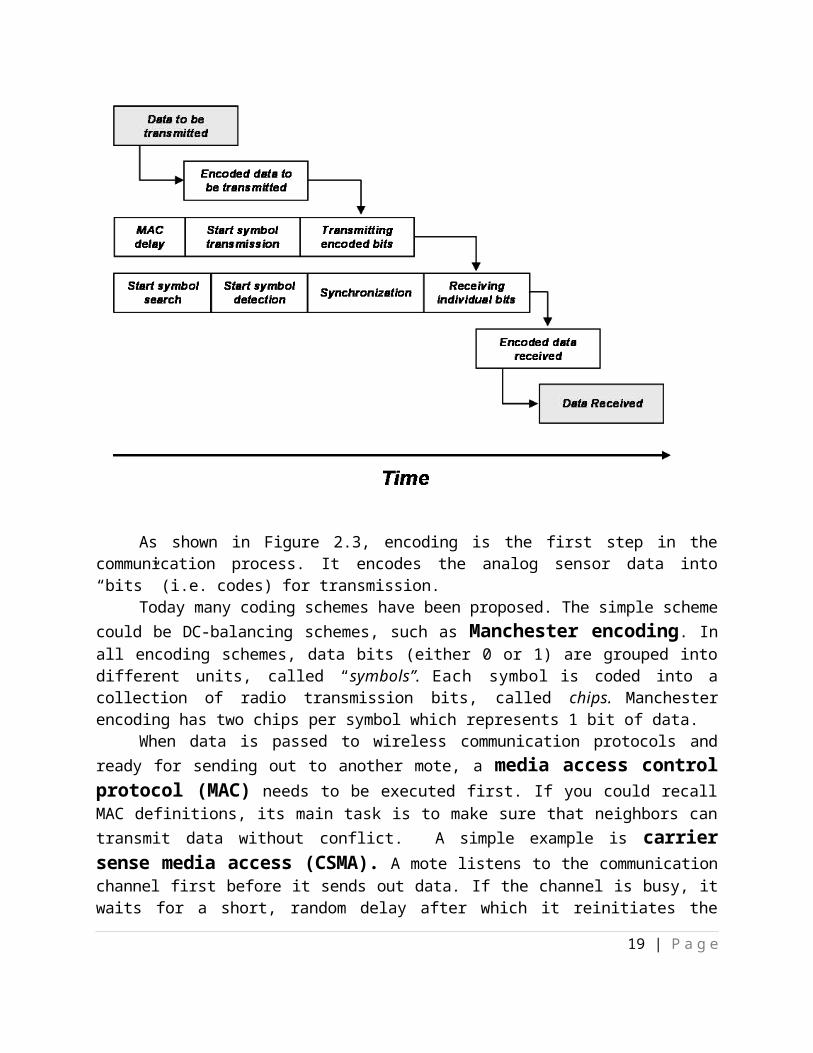
2.2.1.1 - Wireless communication requirements. Figure 2.3 illustrates the key phases of a packet-based wireless communication protocol.
Please note that many of the operations must be performed in parallel with each other.
As shown in Figure 2.3, encoding is the first step in the communication process. It encodes the analog sensor data into “bits” (i.e. codes) for transmission.
Today many coding schemes have been proposed. The simple scheme could be DC-balancing schemes, such as Manchester encoding. In all encoding schemes, data bits (either 0 or 1) are grouped into different units, called “symbols”. Each symbol is coded into a collection of radio
13 | P a g e

transmission bits, called chips. Manchester encoding has two chips per symbol which represents 1 bit of data.
When data is passed to wireless communication protocols and ready for sending out to another mote, a media access control protocol (MAC) needs to be executed first. If you could recall MAC definitions, its main task is to make sure that neighbors can transmit data without conflict. A simple example is carrier sense media access (CSMA). A mote listens to the communication channel first before it sends out data. If the channel is busy, it waits for a short, random delay after which it reinitiates the transmission.
After the MAC protocol successfully sends out data, the Routing Layer protocols will take care of the data from mote to mote. It finds out an optimal path (from energy saving viewpoint) to deliver the data to the destination (such as a base-station).
When data continuously flows between a sender and a receiver, based on accurate time synchronization scheme, the sender precisely controls the timing of each bit transition so that the receiver can maintain synchronization.
When a receiver gets the data, it uses decoding and demodulation to recover original data. Noise is removed by some data cleaning algorithms.
(3) Decoupling between RF and processing speed
The mote architecture must allow a decoupling between RF transmission rates and CPU processing speed. This is because CPU and RF transceiver have very different optimization requirements: (1) A radio prefers to send out data at its maximum transmission rate. This is because a shorter transmitting time reduces the energy used. (2) On the other hand, modern studies in low power CPU design and dynamic voltage scaling have disclosed a fact: CPUs prefer to spread computation out in time as much as possible so that they can run at the lowest possible voltage.
Therefore, from energy saving perspective, it would be preferred that the CPU perform all calculations as slowly as possible and just as the computation is complete, the radio would burst out the data as quickly as possible.
Now we know the decoupling between CPU and radio is important since it allows the above different operation patterns: CPU slowly processes data and radio quickly sends out data. When the speed of the microcontroller is coupled to the data transmission rate, both pieces of the system are forced to operate at non-optimal points.
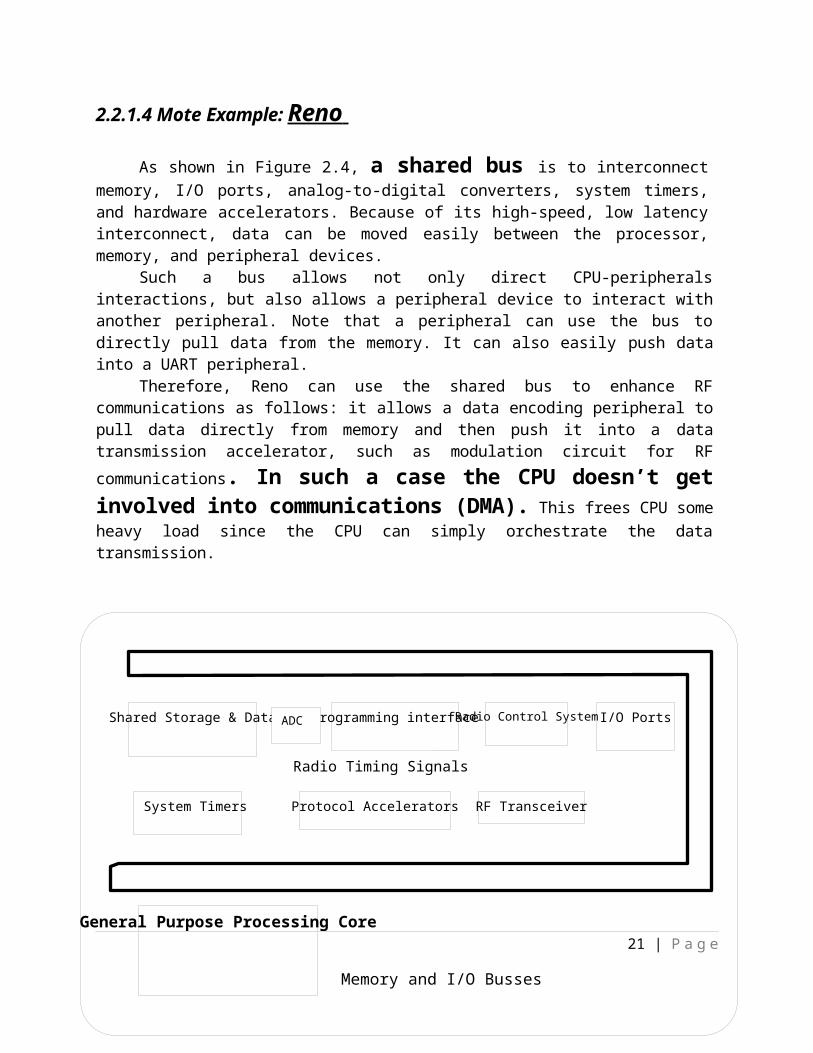
2.2.1.4 Mote Example: Reno
As shown in Figure 2.4, a shared bus is to interconnect memory, I/O ports, analog-to-digital converters, system timers, and hardware accelerators. Because of its high-speed, low latency interconnect, data can be moved easily between the processor, memory, and peripheral devices.
Such a bus allows not only direct CPU-peripherals interactions, but also allows a peripheral device to interact with another peripheral. Note that a peripheral can use the bus to directly pull data from the memory. It can also easily push data into a UART peripheral.
14 | P a g e

Memory and I/O Busses
Protocol Accelerators
General Purpose Processing Core
System Timers RF Transceiver
I/O PortsProgramming interfaceShared Storage & Data ADC Radio Control System
Radio Timing Signals
Therefore, Reno can use the shared bus to enhance RF communications as follows: it allows a data encoding peripheral to pull data directly from memory and then push it into a data transmission accelerator, such as modulation circuit for RF communications. In such a case the CPU doesn’t get involved into communications (DMA). This frees CPU some heavy load since the CPU can simply orchestrate the data transmission.
Figure 2.4 Generalized Architecture for embedded wireless device [Jason03]
If you could recall “Computer Architecture” course, we could use the same addressing schemes to name each memory location and other devices. That is, giving a memory address, it could be a real memory location, or it is just the virtual location of a device’s data buffer.
2.3 Mica Mote Design
Mica hardware components include Atmega103 micrcoprocessor (i.e., CPU), a RFM TR1000 radio, external storage, and communication accelerators. The hardware accelerators optionally assist to increase the performance of key
15 | P a g e

Hardware IDMicrocontroller
(Atmega 103)
Coprocessor
Flash MEM
Radio Transceiver
I/O Expansion Connector
Analog I/O Program LinesDigital I/O
Transmission Power Control
Hardware Accelerators
phases of the wireless communication.Figure 2.5 shows the Mica architecture. It shows five major function modules: CPU, radio
frequency (RF) communication, power management, I/O expansion, and secondary storage. In http://www.tinyos.net the readers could find a quick survey of the major modules, a general overview for the system as a whole, and a detailed bill of materials, device schematic and datasheet for all hardware components.
Figure 2.5 - Block diagram of Mica architecture. The direct connection between application controller and transceiver allows the Mica node to be highly flexible to application demands. Hardware
accelerations optionally assist in communication protocols. [Jason03]
Mica mote uses Atmel ATMEGA103L or ATMEGA128 (4 MHz). Such a CPU also connects a 128-Kbyte flash program memory, 4-Kbyte static RAM, internal 8-channel 10-bit analog-to-digital converter, three hardware timers, 48 general-purpose I/O lines, one external Universal Asynchronous Receiver Transmitter (UART), and one Serial Peripheral Interface (SPI) port. The Mica radio module consists of an RF Monolithics TR1000 transceiver. But it doesn’t use I2C (Inter-IC) interface.
16 | P a g e

In order to obtain a unique identification for each mote, Mica uses a Maxim DS2401 silicon serial number, which is a low-cost ROM device with a minimal electronic interface without power requirements [Dallas08].
Mica’s I/O subsystem interface consists of a 51-pin expansion connector. Those pins allow the mote to interface with a variety of sensing and programming boards. The 51-pin connector has the following interfaces: 8 analog lines, 8 power control lines, 3 pulse width modulated lines, 2 analog compare lines, 4 external interrupt lines, 1 serial port, a collection of lines dedicated to programming the microcontrollers, and some bus interfaces.
Mica uses TR1000 radio to allow the CPU to directly access to the signal strength of the incoming RF transmission. Such a radio interface also allows the CPU to sample the level of background noise during periods when there is no active data transmission. In multi-hop networking applications, such information (radio signal strength, noise levels) can dramatically improve routing efficiency by selecting links with good signal-to-noise ratios.
Mica allows software to power on / off radio quickly and predictably.
2.4 Customized Mote – SpecAlthough it is a quick and simple way to integrate off-the-shelf components into a mote, from
manufacturing cost, energy consumption and system performance viewpoint, it is more efficient to design a custom integrated solution.
If using off-the-shelf chips, the chip-to-chip communications can sacrifice the system delay and power performance due to interface overhead. Therefore, [Jason03] developed a custom ASIC for mote board, which is called Spec. By designing the customized silicon it achieves orders-of-magnitude efficiency improvements on key communication primitives.
Spec is much smaller than off-the-shelf motes. It is just 2.5 mm on a side in a 0.25 um CMOS process even though it integrates a microcontroller, SRAM, communication accelerators and a 900 MHz multi-channel transmitter.
Of course, although its CPU, RF transceiver, memory are based on single-chip design, it still needs some low-cost external components, which include a crystal, battery, inductor and an antenna to be a complete WSN mote.
Spec has a general architecture as shown in Figure 2.7. [Jason03] first used the VHDL digital logic tools to synthesize Spec’s behavioral characteristics. After VHDL simulation, they map the high-level VHDL code into standard cells provided by National Semiconductor using Ambit Build Gates. Its layout was performed with Silicon Ensemble – a tool from Cadence Design Systems. In addition to VHDL simulation, the functionality of the Spec core was also verified by downloading it onto a Xilinx FPGA.
17 | P a g e

System Timers Encryption Engine
Instruction Fetch & Decode
RISC Core
ALURegister File
Radio Subsystem & Analog RF I/O Ports
Memory & I/O Bus
ADCAddress Translation
RAM Blocks
SPI Programming Module
Spec’s data processing speed is much higher than Mica in many applications.
Figure 2.7- Block Diagram of Spec, the single chip wireless mote [Jason03]
2.5 - COTS Dust Systems [Seth00]
In [Seth00], several interesting sensor systems were built. Its mote used the Atmel AT90LS8535 (as the microcontroller) and RF Monolithics 916MHz RF transceiver. The mote controls 7 different types of analog sensors (temperature, light, barometric pressure, 2-axis acceleration, and 2-axis magnetometers). Regarding the power source, it uses a single 3-V lithium coin cell battery. It can operate for five days of continuous operation or 1.5 years at 1% duty cycling.
18 | P a g e
Listen for Stop Signal 30 msTransmit Data 43 msListen for query 100 ms
Yes
Yes
No
Send Data to Computer 1 msTransmit Query 35 ms Listen for Sensor Data 100ms Yes
No
Floating Mote Protocol
Base Mote Protocol
Data Received?
Stop Signal Received ?Query Received ?
Figure 2.8 shows its single-hop communication protocol,
Figure 2.8 - Protocols used for Base and Floating Mote [seth00]
2.6 - Telos mote [Joseph05] -- Show Xbow.com website
The Telos- series mote (such as Telos-B) is popularly used sensor platform today. Figure 2.9 shows an example. Unlike Spec that integrates the design into silicon, Telos uses COTS components with hardware accelerators to build a power efficient system that does not sacrifice performance.
19 | P a g e

Figure 2.9 Telos (a type of mote) with IEEE 802.15.4 wireless transceiver. [Joseph05]
After comparing the CPU performance from Atmel, Motorola, and Microchip, Telos developers select MSP430 CPU due to its following advantages:
(1) It has lowest power consumption in sleep and active modes (see Table 2.8). (2) It can tolerate a low operation voltage of 1.8V. If we use other CPUs, say
ATmega128 MCU (Mica family), it can only run down to 2.7V, leaving almost 50% of the AA batteries unused.
(3) We know that a faster wake-up time helps to conserve energy. takes <6μs (4) From memory viewpoint, Table 2.8 shows that the MSP430 has the largest on-
chip RAM buffer (10kB). It is good for on-chip signal processing. A larger RAM allows more sophisticated applications.
From RF communication viewpoint, Telos has the following features:(1) It uses the IEEE 802.15.4 standard. Such a standardized radio allows a Telos
to communicate with many radio devices from other vendors. (2) It uses the Chipcon CC2420 radio. It uses 2.4GHz RF band, a wideband radio with O-
QPSK modulation with DSSS at 250kbps. Such a high data rate (other motes typically operates under 150kbps) shortens the operation time (which helps to reduce energy consumption).
2.7 - CargoNet [Mateusz07]
In [Mateusz07] a mote, called CargoNet, is designed to bridge the gap between WSNs and radio frequency identification (RFID).
20 | P a g e
The CargoNet nodes uses a new concept, called Quasi-Passive Wakeup, to achieve an asynchronous, multi-modal wakeup, which can wake up (from sleep mode) to perform extremely low power operations.
CargoNet uses external stimuli signals to wake up its sensor mote. This idea is not new. For instance, researchers at Northwestern University have used a similar wake-up strategy for vibration detection and autonomous crack monitoring. Their platform uses a single geophone as the input sensor, and wakes up to record aperiodic shocks to ensure structural integrity of buildings.
Radio-frequency identification (RFID), aims to improve traditional barcodes when used in the transport and distribution of goods. Traditional bar codes require line-of-sight between interrogator and tagged object. Therefore human operators must align a tagged object to ensure a successful read. Moreover, those bar codes have very short information. The distance between the interrogator and bar codes is very short (typically a few centimeters).
On the other hand, RFID uses a reader to read tags that are attached in products. The distance between the reader and tags could be even a few meters depending on the used radio frequency. Moreover, the reader can read a tag’s data through non-light-of-sight signals that propagates widely and permeates through most nonconductive materials, allowing identification without human involvement. While traditional bar code is printed onto a surface and cannot be changed, we can change the data in RFID tags since they are electronic circuits that can change state based on external stimuli.
A concept, called “active RFID”, has been proposed recently. It is actually a special sensor device that has battery and CPUs to provide better “visibility” into their supply chains. “Active RFIDs” can accurately collect data about environmental conditions experienced by goods in transit, and better manage risk and maintain flexibility. It can detect potentially damaged goods before they reach their destination and reordered if necessary.
CargoNet node is such a type of “active RFID”. Its “quasi-passive wakeup” is based on the following interesting fact: the external stimuli could actually be used to wake up and even provide energy to the CPU! It desensitizes the sensors following repeating stimuli. This further reduces frequency of redundant wakeup to save power. Quasi-passive wakeup allows a cargonet RFID tag to simultaneously and continuously monitor many sensor modalities for exceptional activity while dissipating minimal power.
Figure 2.10 is a system diagram with the CargoNet “active RFID” tags and RFID reader. Its core hardware consists of the MSP430 microcontroller, real-time-clock, and CC2500 2.4GHz radio. The MSP430F135 flash-based microcontroller is made from Texas Instruments (TI). It has a specified standby current of less than 0.1µA when entering sleep state.
21 | P a g e

Figure 2.10 - CargoNet system diagram [Mateusz07]
The “active RFID” tags use the CC2500 from Chipcon to communicate wirelessly with RFID readers/interrogators. Different from traditional RFID systems, the CC2500 radio is fully bidirectional, such that the “active RFID” tags can also receive instructions from the RFID readers besides sending tag data to the reader. This feature bridges the gap between the “active RFID” and WSNs since WSN motes requires bi-directional communications between nodes. Such a bi-directional radio communication capability enables useful applications, such as synchronizing clocks, recording the identity of neighbors, or qualifying the validity of sensor readings.
CargoNet system also uses the following two sensors, the RF wakeup receiver and “vibration dosimeter”. They have linear amplifiers to boost or integrate weak signals.
Table 2.9 lists CargoNet sensors that assemble a suite of measurements relevant to the transport of equipment and goods.
Sensor Type Measurement or Application
Shock Sensor Potential impact damage
Vibration Dosimeter Average low-level vibrations
Tilt Switch Package orientation and shaking
Piezo Microphone Events causing loud nearby sounds
Light Sensor Container breach or box opening
22 | P a g e

Magnetic Switch Package removed or box opened
Temperature Sensor Overheating or potential spoilage
Humidity Sensor Potential moisture damage
RF Wakeup Query from reader or another tag
Table 2.9 - CargoNet sensor types [Mateusz07]
Now let’s provide more details on CargoNet’s “Quasi-passive wakeup” strategy. Figure 2.11 shows its basic wake-up procedure. After an “active RFID” tag receives a stimulus signal, it compares the results against a threshold. If the stimulus is strong enough to warrant interest, the tag wakes up a larger system.
23 | P a g e
Good Idea
Normally people distinguish RFID from mote very clearly. But CargoNet designs a device that can serve as both RFID tag and a WSN node. It can collect data from environment into a “tag”, and then let a RFID reader to remotely read such data. The reason we use “active RFID” here is because CargoNet makes its RFID tag battery-driven and have close performance to an intelligent sensor node.