ECE 331: Introduction to Materials for Electrical Engineersringel/331...
15
ECE 331: Introduction to Materials for Electrical Engineers Course Objective... Introduce fundamental concepts in Materials Introduce fundamental concepts in Materials Science and how they are used in ECE You will learn about: • material structure • how structure dictates properties • how electronic & physical properties are related • how electronic & physical properties are related This course will help you to: • use materials properly • use materials properly • realize new design opportunities with materials • understand the physics of semiconductor devices ECE331 Wi11 lecture 1
Transcript of ECE 331: Introduction to Materials for Electrical Engineersringel/331...
ECE 331: Introduction to Materials for Electrical Engineers
Course Objective...Introduce fundamental concepts in MaterialsIntroduce fundamental concepts in MaterialsScience and how they are used in ECE
You will learn about:• material structure• how structure dictates properties• how electronic & physical properties are related• how electronic & physical properties are related
This course will help you to:• use materials properly• use materials properly• realize new design opportunities with materials• understand the physics of semiconductor devices
ECE331 Wi11 lecture 1
ECE 331 – Intro to Materials for ECE
Materials in ECE are: semiconductors, metals (e.g. Al t t ) l ( l t f LED )Al contacts), polymers (e.g. encapsulants for LEDs) and insulators (ceramics such as silicon dioxide in FETs))
Materials in ECE are single crystals, polycrystals, h l d t tamorphous layers and nanostructures
Si (silicon) is NOT the only semiconductor (thoughSi (silicon) is NOT the only semiconductor (though Si electronics is the world’s largest manufacturing industry), but it is the most important one and will
i !
ECE331 Wi11 lecture 1
remain so!

ECE 331 – Intro to Materials for ECE
III-V examplesGaAsInPInAsAlGaAsAlGaAsInGaAsInGaAsPG NGaNInGaN
ECE331 Wi11 lecture 1
III - V•Know your periodic table!•Find your old chemistry notes!

Materials Roadmap for Device Technologies: the Bandgap vs Lattice Constant Relationship
III-V electronics
ECE applications areexpanding acrossIII V electronics
CD LasersFiber pump lasersSpace solar
expanding across this entire space!
CMOS BiCMOSCMOS, BiCMOS,Terrestrial solar,Power CMOS
TelecommOptoelectronicsthermophotovoltaics
ECE331 Wi11 lecture 1

TECHNOLOGY ROADMAPS: New Age for ECE Materials and opportunities
• Electronics:
Roadmaps are calling for unusual properties not obtainable using conventional materials or processes• Electronics:
- Nanoscale patterning- optical interconnects- speed enhancing materials
• Optoelectronics:Optoelectronics: - tunable light emission/detection wavelengths- seamless integration with electronic systems
• Alternative Energy:- clean, renewable, cheap, safe, autonomous
ECE331 Wi11 lecture 1
- Biocompatiblity and medicine
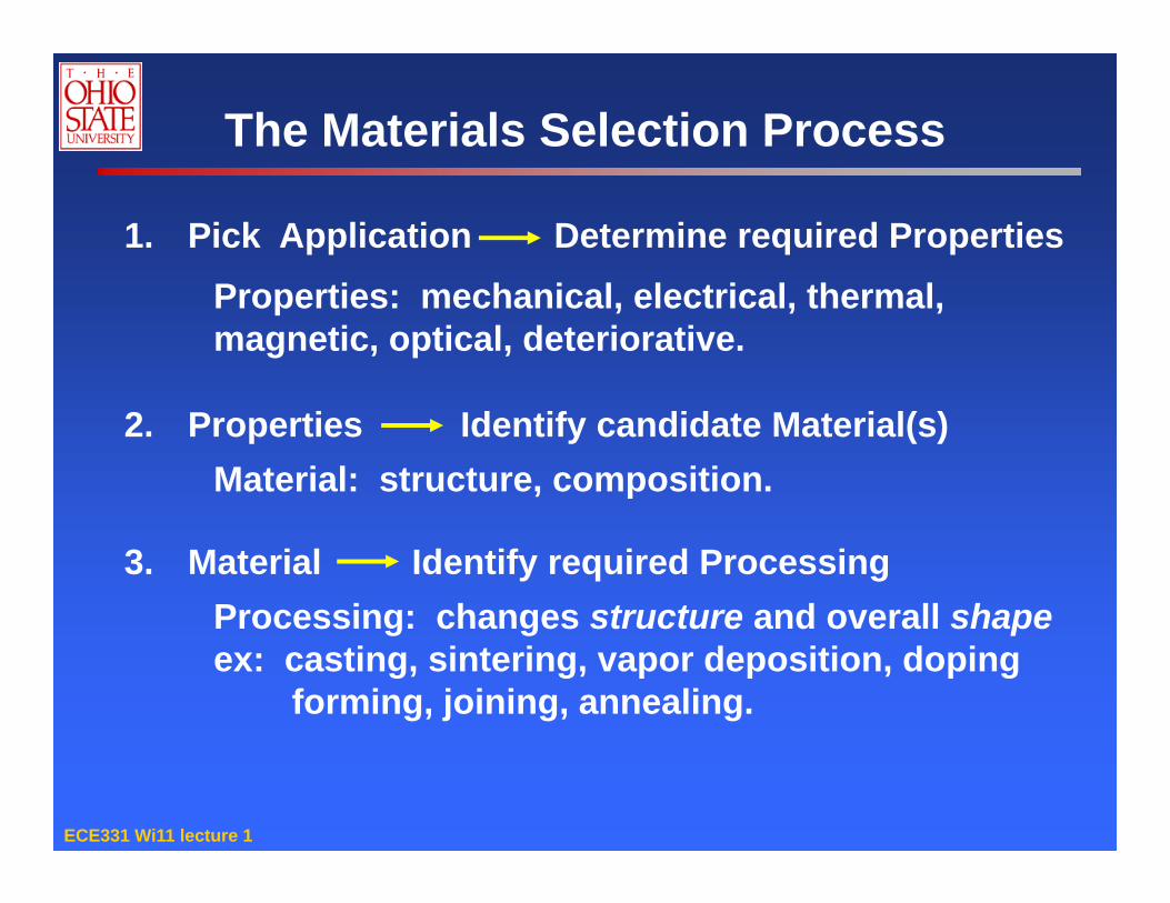
The Materials Selection Process
1. Pick Application Determine required PropertiesProperties: mechanical, electrical, thermal,magnetic, optical, deteriorative.
2. Properties Identify candidate Material(s)Material: structure, composition.
3. Material Identify required ProcessingProcessing: changes structure and overall shapeProcessing: changes structure and overall shapeex: casting, sintering, vapor deposition, doping
forming, joining, annealing.
ECE331 Wi11 lecture 1

ELECTRICAL• Electrical Resistivity of Copper:
Adapted from Fig. 18.8, Callister 7e.6 g(Fig. 18.8 adapted from: J.O. Linde,Ann Physik 5, 219 (1932); andC.A. Wert and R.M. Thomson,Physics of Solids, 2nd edition,McGraw-Hill Company, New York,1970 )
4
5
y, r
m)
1970.)
2
3
esis
tivit
0-8
Ohm
-
1
2
Re (10
0
• Adding “impurity” atoms to Cu increases resistivity.
T (°C)-200 -100 00
ECE331 Wi11 lecture 1
• Deforming Cu increases resistivity.
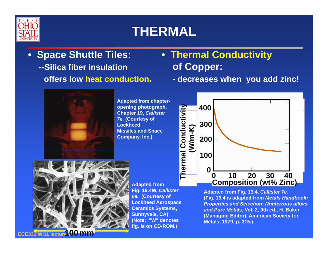
THERMAL• Space Shuttle Tiles:
--Silica fiber insulationoffers low heat conduction
• Thermal Conductivityof Copper:
decreases when you add zinc!offers low heat conduction. - decreases when you add zinc!
ity
400Adapted from chapter-opening photograph,
ondu
ctiv
i/m
-K) 300
200
Chapter 19, Callister 7e. (Courtesy of LockheedMissiles and SpaceCompany, Inc.)
herm
al C
o(W
/
100
00 10 20 30 40
Adapted fromFig. 19.4W, Callister 6e. (Courtesy of Lockheed Aerospace C S
Adapted from Fig. 19.4, Callister 7e.(Fig. 19.4 is adapted from Metals Handbook: Properties and Selection: Nonferrous alloys
Composition (wt% Zinc)Th 0 10 20 30 40
ECE331 Wi11 lecture 1
Ceramics Systems, Sunnyvale, CA)(Note: "W" denotes fig. is on CD-ROM.)
p yand Pure Metals, Vol. 2, 9th ed., H. Baker, (Managing Editor), American Society for Metals, 1979, p. 315.)
100mm
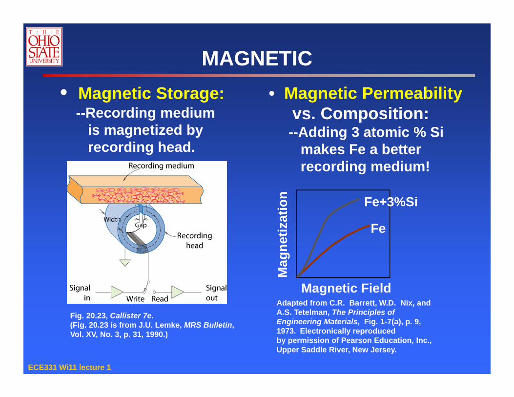
MAGNETIC• Magnetic Permeability
vs. Composition:• Magnetic Storage:
--Recording medium--Adding 3 atomic % Si
makes Fe a betterrecording medium!
is magnetized byrecording head.
g
zatio
n Fe+3%Si
F
Mag
netiz Fe
Adapted from C.R. Barrett, W.D. Nix, andA.S. Tetelman, The Principles ofEngineering Materials, Fig. 1-7(a), p. 9,
Fig. 20.23, Callister 7e.(Fig 20 23 is from J U Lemke MRS Bulletin
Magnetic FieldM
ECE331 Wi11 lecture 1
Engineering Materials, Fig. 1 7(a), p. 9,1973. Electronically reproducedby permission of Pearson Education, Inc.,Upper Saddle River, New Jersey.
(Fig. 20.23 is from J.U. Lemke, MRS Bulletin,Vol. XV, No. 3, p. 31, 1990.)
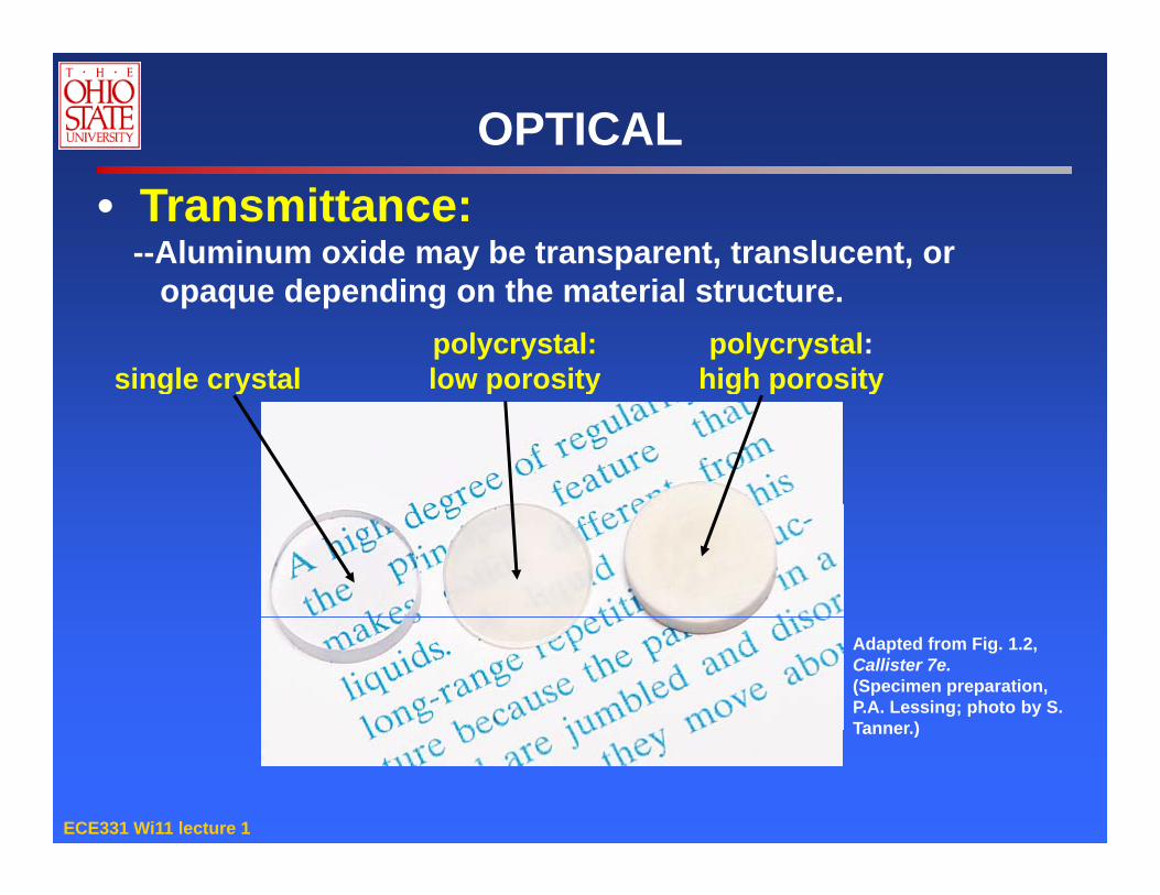
OPTICAL• Transmittance:
--Aluminum oxide may be transparent, translucent, oropaque depending on the material structure.
single crystalpolycrystal:low porosity
polycrystal:high porosityg y p y g p y
Adapted from Fig. 1.2,Callister 7e.(Specimen preparation,P.A. Lessing; photo by S. Tanner )
ECE331 Wi11 lecture 1
Tanner.)
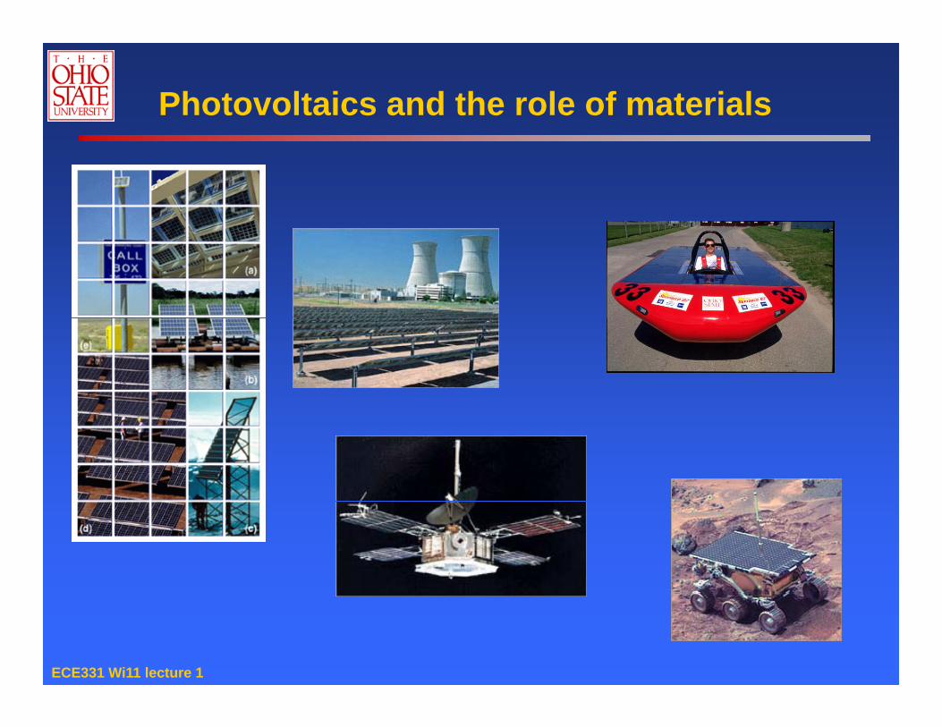
Photovoltaics and the role of materials
ECE331 Wi11 lecture 1
ECE331 Wi11 lecture 1

Conversion of radiant heat to electricity: Thermophotovoltaics
InterconnectGrid Finger
Front Contact
p
n InPAs window
p InPAs BSF
S i I l ti I P
n InPAs Bufferp/n InGaAs TJ
n/p InGaAsEmitter/Base
Semi-Insulating InP
SiN/Gold Back Surface Reflector
23
SEM Micrograph Of Processed TernaryMIM Structure
1920212223
ficie
ncy
(%)
26.7°C26.7°C
25.6°C
• Efficiency ~18%
• With addition of a a front surface filter
1516171819
Syst
em E
ff25.6°C
surface filter – 0.9 W/cm2 power density- h = 20.6% at a radiator
temperat re of 1058°C
ECE331 Wi11 lecture 1
850 900 950 1000 1050 1100
Radiator Temperature (°C)
temperature of 1058°C.

Wide Bandgap Semiconductors – GaN: Energy-Efficient Solid State Lighting (SSL)gy g g ( )
• Al-Ga-In-N spans uv-blue-green-red-near ir spectrum
50% of elec used by lighting:
National SSL Initiative: by 2020:• save $115B
ECE331 Wi11 lecture 1
50% of elec.used by lighting: • eliminate 258M metric ton of C emission

SUMMARY
• Use the right material for the job
Course Goals:
• Use the right material for the job.
• Understand the relation between properties,structure, and processing.
• Recognize new design opportunities offered• Recognize new design opportunities offeredby materials selection.
• Appreciate the relationship between devices• Appreciate the relationship between devices, their characteristics and their constituent materials
ECE331 Wi11 lecture 1