Data sheet SM 331 (331-1KF01) Technical data Order no. 331 ...
Upload
eileen-payneCategory
view
230download
2
ECE 331 – Digital System Design
Transistor Technologies,and
Realizing Logic Gates using CMOS Circuits
(Lecture #23)

ECE 331 - Digital System Design 2
Transistor Technologies
Two transistor technologies:
1. Transistor-Transistor Logic (TTL)2. Metal Oxide Semiconductor (MOS)

ECE 331 - Digital System Design 3
TTL Technology
TTL = Transistor-transistor Logic Dominant technology prior to the emergence of
CMOS technology. Not as suitable for large-scale integration as
CMOS technology. Largely obsolete for new designs.
Good for labs and educational use because it is more robust than CMOS.

ECE 331 - Digital System Design 4
TTL Technology Bipolar Junction Transistor (BJT)
Base – controls current flow in transistor Collector – current flow enters transistor Emitter – current flow exits transistor
npn BJT Collector, Emitter: n-type semiconductor Base: p-type semiconductor
pnp BJT Collector, Emitter: p-type semiconductor Base: n-type semiconductor

ECE 331 - Digital System Design 5
MOS Technology CMOS
Complementary Metal Oxide Semiconductor NMOS
N-channel MOSFET PMOS
P-channel MOSFET MOSFET
Metal Oxide Semiconductor Field Effect Transistor

ECE 331 - Digital System Design 6
Drain Source
x = "low" x = "high"
(a) A simple switch controlled by the input x
V D V S
(b) NMOS transistor
Gate
(c) Simplified symbol for an NMOS transistor
V G
Substrate (Body)
NMOS Transistor

ECE 331 - Digital System Design 7
NMOS Transistor
Four-terminal device Simplified three-terminal representation
Conducting channel is N-type material Drain pulled high (connected to supply voltage)
in digital circuits Source pulled low (connected to ground) in
digital circuits

ECE 331 - Digital System Design 8
NMOS Transistor
Gate-to-Source Voltage (VGS
)
Controls the drain current (iD) via an electric
field Oxide (silicon dioxide) insulates the gate from
the drain and the source i
G ~= 0 Amps
iD ~= i
S
Low power

ECE 331 - Digital System Design 9
NMOS Transistor
Operates as a binary switch in digital circuits V
G = 0V (V
S = GND = 0V)
VGS
~= 0V
“looks like” an open switch (in the cutoff region; “off”)
ID = I
S = 0A
VG = VDD (V
S = GND = 0V)
VGS
~= VDD
“looks like” a closed switch (in the saturated region; “on”)

ECE 331 - Digital System Design 10
Gate
x = "high" x = "low"
(a) A switch with the opposite behavior of the NMOS transistor
V G
V D V S
(b) PMOS transistor
(c) Simplified symbol for a PMOS transistor
V DD
Drain Source
Substrate (Body)
PMOS Transistor

ECE 331 - Digital System Design 11
PMOS Transistor
Four-terminal device Three-terminal simplified representation
Conducting channel is P-type material Drain pulled low (connected to ground) in digital
circuits Source pulled high (connected to supply
voltage) in digital circuits

ECE 331 - Digital System Design 12
PMOS Transistor
Gate-to-Source Voltage (VGS
)
Controls the drain current (iD) via an electric
field Oxide (silicon dioxide) insulates the gate from
the drain and the source i
G ~= 0 Amps
iD ~= i
S
Low power

ECE 331 - Digital System Design 13
PMOS Transistor
Operates as an binary switch in digital circuits V
G = 0V (V
S = VDD = Supply Voltage)
VGS
~= -VDD (VSG
~= VDD)
“looks like” an closed switch (in the saturated region; “on”)
VG = VDD (V
S = VDD = Supply Voltage)
VGS
~= 0V (VSG
= 0V)
“looks like” a open switch (in the cutoff region; “off”)
ID = I
S = 0A

ECE 331 - Digital System Design 14
(a) NMOS transistor
V G
V D
V S = 0 V
V S = V DD
V D
V G
Closed switch when V G = V DD
V D = 0 V
Open switch when V G = 0 V
V D
Open switch when V G = V DD
V D
V DD
Closed switch when V G = 0 V
V D = V DD
V DD
(b) PMOS transistor
NMOS and PMOS Transistors

ECE 331 - Digital System Design 15
V f
V DD
Pull-down network
Pull-up network
V x 1
V x n
(PUN)
(PDN) NMOS transistors
PMOS transistors
CMOS Logic Circuit

ECE 331 - Digital System Design 16
Voltage Levels in CMOS Circuits
Voltages are used to represent Logic values in CMOS (and TTL) circuits:
Logic 1 = VDDLogic 0 = GND

ECE 331 - Digital System Design 17
Voltage Ranges in CMOS Circuits
Logic value 1
Undefined
Logic value 0
Voltage
V DD
V 1,min
V 0,max
V SS (Gnd)
ECE 331 - Digital System Design 18
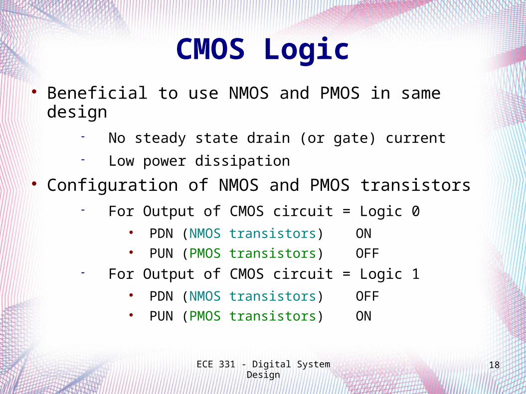
CMOS Logic Beneficial to use NMOS and PMOS in same design
No steady state drain (or gate) current Low power dissipation
Configuration of NMOS and PMOS transistors For Output of CMOS circuit = Logic 0
PDN (NMOS transistors) ON PUN (PMOS transistors) OFF
For Output of CMOS circuit = Logic 1 PDN (NMOS transistors) OFF PUN (PMOS transistors) ON

ECE 331 - Digital System Design 19
(a) Circuit
V f
V DD
V x
(b) Truth table and transistor states
T 1
T 2
on
off
off
on
1
0
0
1
f x T 1 T 2
CMOS Circuit: Inverter (NOT)

ECE 331 - Digital System Design 20
CMOS Circuit: NAND Gate
(a) Circuit
V f
V DD
(b) Truth table and transistor states
on
on
on
off
0
1
0
0
1
1
0
1
off
off
on
off
off
on
f
off
on
1
1
1
0
off
off on
on
V x 1
V x 2
T 1 T 2
T 3
T 4
x 1 x 2 T 1 T 2 T 3 T 4

ECE 331 - Digital System Design 21
CMOS Circuit: NOR Gate
(a) Circuit
V f
V DD
(b) Truth table and transistor states
on
on
on
off
0
1
0
0
1
1
0
1
off
off
on
off
off
on
f
off
on
1
0
0
0
off
off on
on
V x 1
V x 2
T 1
T 2
T 3 T 4
x 1 x 2 T 1 T 2 T 3 T 4

ECE 331 - Digital System Design 22
V f
V DD
V x 1
V x 2
V DD
CMOS Circuit: AND Gate
NAND Gate
Inverter

ECE 331 - Digital System Design 23
CMOS Circuit: OR Gate

ECE 331 - Digital System Design 24
CMOS Circuits
Analysis

ECE 331 - Digital System Design 25
The functional behavior of a CMOS circuit can be determined by analyzing the behavior of the
individual PMOS and NMOS transistors, and, thus, the behavior of the PUN and PDN.
CMOS Circuits: Analysis
ECE 331 - Digital System Design 26
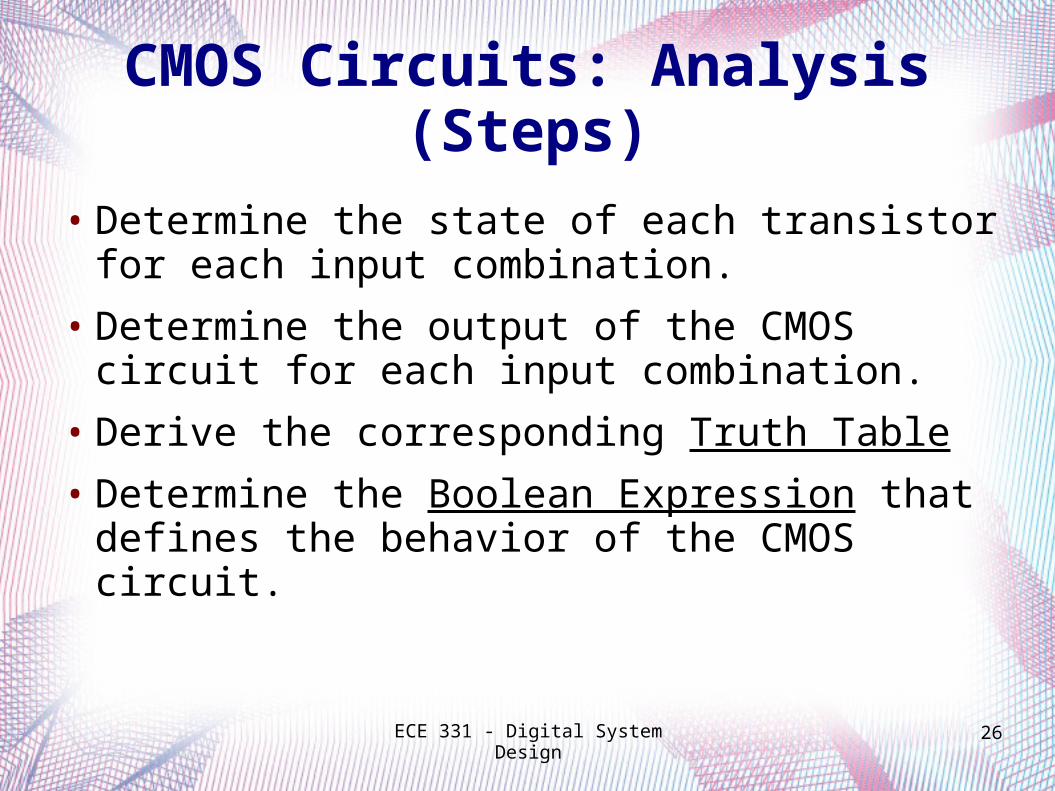
CMOS Circuits: Analysis (Steps)
• Determine the state of each transistor for each input combination.
• Determine the output of the CMOS circuit for each input combination.
• Derive the corresponding Truth Table
• Determine the Boolean Expression that defines the behavior of the CMOS circuit.

ECE 331 - Digital System Design 27
Example #1:
Analyze the following CMOS circuit to determine the logic function that it implements.
CMOS Circuits: Analysis

ECE 331 - Digital System Design 28
CMOS Circuit: Analysis (Ex. #1)

ECE 331 - Digital System Design 29
Example #2:
Analyze the following CMOS circuit to determine the logic function that it implements.
CMOS Circuits: Analysis

ECE 331 - Digital System Design 30
CMOS Circuit: Analysis (Ex. #2)