
DSC400-1111Q0085 -...
10
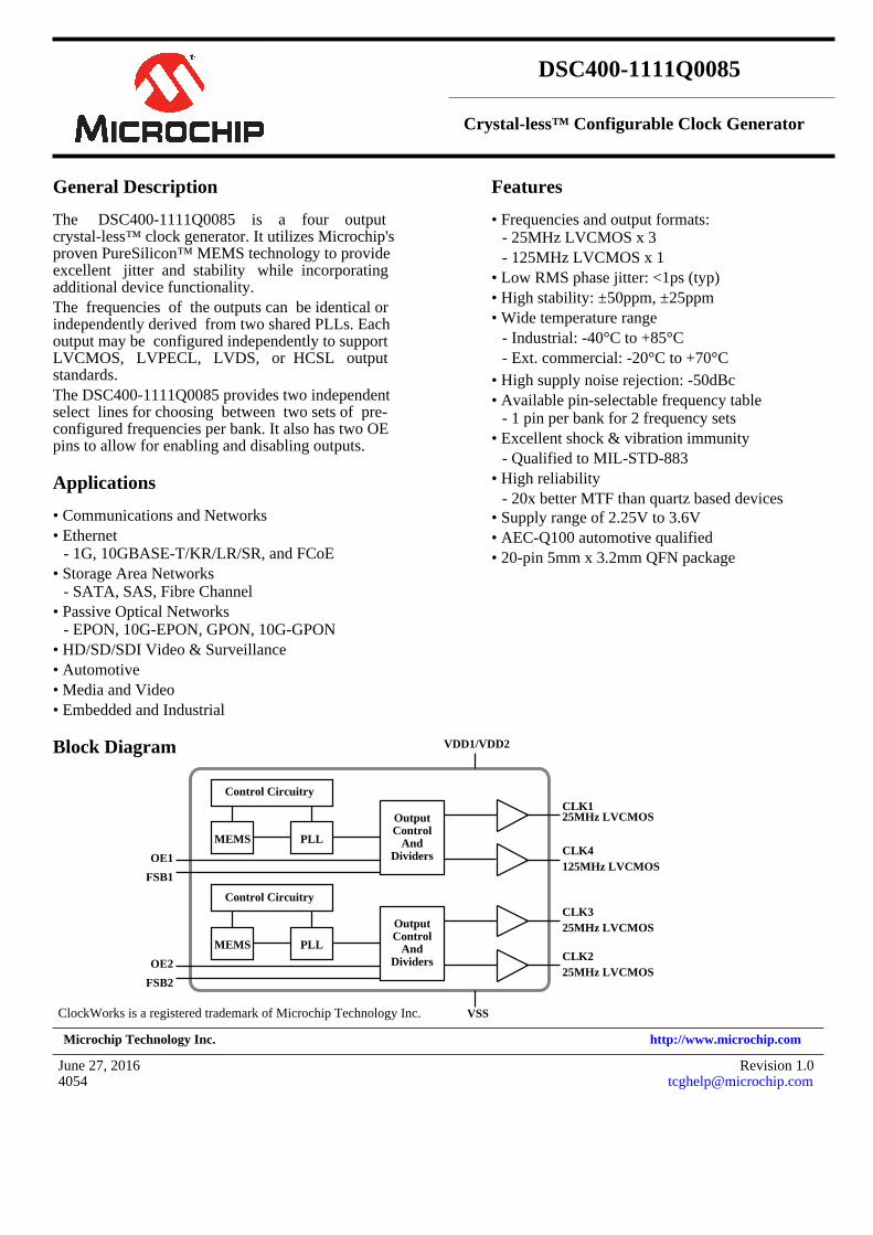
DSC400-1111Q0085 Crystal-less™ Configurable Clock Generator General Description The DSC400-1111Q0085 is a four output crystal-less™ clock generator. It utilizes Microchip's proven PureSilicon™ MEMS technology to provide excellent jitter and stability while incorporating additional device functionality. The frequencies of the outputs can be identical or independently derived from two shared PLLs. Each output may be configured independently to support LVCMOS, LVPECL, LVDS, or HCSL output standards. The DSC400-1111Q0085 provides two independent select lines for choosing between two sets of pre- configured frequencies per bank. It also has two OE pins to allow for enabling and disabling outputs. Applications • Communications and Networks • Ethernet - 1G, 10GBASE-T/KR/LR/SR, and FCoE • Storage Area Networks - SATA, SAS, Fibre Channel • Passive Optical Networks - EPON, 10G-EPON, GPON, 10G-GPON • HD/SD/SDI Video & Surveillance • Automotive • Media and Video • Embedded and Industrial Features • Frequencies and output formats: - 25MHz LVCMOS x 3 - 125MHz LVCMOS x 1 • Low RMS phase jitter: <1ps (typ) • High stability: ±50ppm, ±25ppm • Wide temperature range - Industrial: -40°C to +85°C - Ext. commercial: -20°C to +70°C • High supply noise rejection: -50dBc • Available pin-selectable frequency table - 1 pin per bank for 2 frequency sets • Excellent shock & vibration immunity - Qualified to MIL-STD-883 • High reliability - 20x better MTF than quartz based devices • Supply range of 2.25V to 3.6V • AEC-Q100 automotive qualified • 20-pin 5mm x 3.2mm QFN package Block Diagram VSS VDD1/VDD2 Control Circuitry MEMS PLL Output Control And Dividers OE1 FSB1 OE2 FSB2 Control Circuitry MEMS PLL Output Control And Dividers CLK1 25MHz LVCMOS CLK4 125MHz LVCMOS CLK3 25MHz LVCMOS CLK2 25MHz LVCMOS ClockWorks is a registered trademark of Microchip Technology Inc. Microchip Technology Inc. http://www.microchip.com June 27, 2016 Revision 1.0 [email protected] 4054
Transcript of DSC400-1111Q0085 -...
DSC400-1111Q0085
Crystal-less™ Configurable Clock Generator
General Description
The DSC400-1111Q0085 is a four output crystal-less™ clock generator. It utilizes Microchip'sproven PureSilicon™ MEMS technology to provideexcellent jitter and stability while incorporatingadditional device functionality.The frequencies of the outputs can be identical orindependently derived from two shared PLLs. Eachoutput may be configured independently to supportLVCMOS, LVPECL, LVDS, or HCSL outputstandards.The DSC400-1111Q0085 provides two independentselect lines for choosing between two sets of pre-configured frequencies per bank. It also has two OEpins to allow for enabling and disabling outputs.
Applications
• Communications and Networks• Ethernet
- 1G, 10GBASE-T/KR/LR/SR, and FCoE• Storage Area Networks
- SATA, SAS, Fibre Channel• Passive Optical Networks
- EPON, 10G-EPON, GPON, 10G-GPON• HD/SD/SDI Video & Surveillance• Automotive• Media and Video• Embedded and Industrial
Features
• Frequencies and output formats:- 25MHz LVCMOS x 3- 125MHz LVCMOS x 1
• Low RMS phase jitter: <1ps (typ)• High stability: ±50ppm, ±25ppm• Wide temperature range
- Industrial: -40°C to +85°C- Ext. commercial: -20°C to +70°C
• High supply noise rejection: -50dBc• Available pin-selectable frequency table
- 1 pin per bank for 2 frequency sets• Excellent shock & vibration immunity
- Qualified to MIL-STD-883• High reliability
- 20x better MTF than quartz based devices• Supply range of 2.25V to 3.6V• AEC-Q100 automotive qualified• 20-pin 5mm x 3.2mm QFN package
Block Diagram
VSS
VDD1/VDD2
Control Circuitry
MEMS PLL
OutputControl
AndDividersOE1
FSB1
OE2
FSB2
Control Circuitry
MEMS PLL
OutputControl
AndDividers
CLK125MHz LVCMOS
CLK4125MHz LVCMOS
CLK325MHz LVCMOS
CLK225MHz LVCMOS
ClockWorks is a registered trademark of Microchip Technology Inc.
Microchip Technology Inc. http://www.microchip.com
June 27, 2016 Revision [email protected]

Microchip Technology Inc. DSC400-1111Q0085
Ordering Information
Ordering Part Number Temperature Range High Stability Shipping Package
DSC400-1111Q0085KI1 -40°C to +85°C ±50ppm Tube 20-pin 5mm x 3.2mm QFN
DSC400-1111Q0085KI1T -40°C to +85°C ±50ppm Tape and Reel 20-pin 5mm x 3.2mm QFN
DSC400-1111Q0085KI2 -40°C to +85°C ±25ppm Tube 20-pin 5mm x 3.2mm QFN
DSC400-1111Q0085KI2T -40°C to +85°C ±25ppm Tape and Reel 20-pin 5mm x 3.2mm QFN
DSC400-1111Q0085KE1 -20°C to +70°C ±50ppm Tube 20-pin 5mm x 3.2mm QFN
DSC400-1111Q0085KE1T -20°C to +70°C ±50ppm Tape and Reel 20-pin 5mm x 3.2mm QFN
DSC400-1111Q0085KE2 -20°C to +70°C ±25ppm Tube 20-pin 5mm x 3.2mm QFN
DSC400-1111Q0085KE2T -20°C to +70°C ±25ppm Tape and Reel 20-pin 5mm x 3.2mm QFN
Devices are Green and RoHS compliant. Sample material may have only a partial top mark.
Pin Configuration
20-pin 5mm x 3.2mm QFN
OE1
NC
VSS
VSS
VSS
VSS
NC
OE2
NC
CL
K1
NC
CL
K2
VD
D2
FSB
2
FSB
1
VD
D1
CL
K4
NC
CL
K3
NC
June 27, 2016 2 Revision [email protected]

Microchip Technology Inc. DSC400-1111Q0085
Pin Description
Pin Number Pin Name Pin Type Pin Function
1 OE1 I Output enable for Bank 1 (CLK1 and CLK4); active high - see Table 1
2 NC Leave unconnected or connect to ground
3 VSS PWR Ground
4 VSS PWR Ground
5 NC Leave unconnected or connect to ground
6 CLK1 O LVCMOS output 1 = 25MHz
7 NC Leave unconnected or connect to ground
8 CLK2 O LVCMOS output 2 = 25MHz
9 VDD2 PWR Power supply for Bank 2 (CLK3 and CLK2)
10 FSB2 IInput for selecting pre-configured frequencies on Bank 2 (CLK3 and CLK2)No connect if the function is not used.
11 OE2 I Output enable for Bank 2 (CLK3 and CLK2); active high - see Table 1
12 NC Leave unconnected or connect to ground
13 VSS PWR Ground
14 VSS PWR Ground
15 NC Leave unconnected or connect to ground
16 CLK3 O LVCMOS output 3 = 25MHz
17 NC Leave unconnected or connect to ground
18 CLK4 O LVCMOS output 4 = 125MHz
19 VDD1 PWR Power supply for Bank 1 (CLK1 and CLK4)
20 FSB1 IInput for selecting pre-configured frequencies on Bank 1 (CLK1 and CLK4)No connect if the function is not used.
June 27, 2016 3 Revision [email protected]

Microchip Technology Inc. DSC400-1111Q0085
Operational Description
The DSC400-1111Q0085 is a crystal-less™ clock generator. Unlike older clock generators in the industry, it does not require anexternal crystal to operate; it relies on integrated MEMS resonators that interface with internal PLLs. This technology enhancesperformance and reliability by allowing tighter frequency stability over a far wider temperature range. In addition, the higherresistance to shock and vibration decreases the aging rate, greatly improving product life in the system.
Inputs
There are 4 input signals in the device. Each has an internal (40kOhms) pull up, which defaults the selection to a high (1). Inputscan be controlled through hardware strapping method with a resistor to ground to assert the input low (0). Inputs may also becontrolled by other components' GPIOs. In case more than one frequency set is desired, FSB1 and FSB2 are used for independent-ly selecting one of two sets frequency per bank. FSB1 selects the pre-configured frequency set on Bank 1 (CLK1 and CLK4) andFSB2 selects the pre-configured frequency set on Bank 2 (CLK3 and CLK2). If there is a requirement to disable outputs, theinputs OE1 and OE2 are used to disable the banks of outputs. Outputs are disabled in tristate (Hi-Z) mode, see Table 1 below.
OE1 OE2 Bank 1 (CLK1 and CLK4) Bank 2 (CLK3 and CLK2)
0 0 Hi-Z Hi-Z
0 1 Hi-Z Running
1 0 Running Hi-Z
1 1 Running Running
Table 1. Output Enable (OE) Selection Table
Outputs
The four outputs are grouped into two banks. Each bank is supplied by an independent VDD to allow for optimized noiseisolation between the two banks. Each bank provides two synchronous outputs generated by a common PLL:
• Bank 1 is composed of outputs CLK1 and CLK4• Bank 2 is composed of outputs CLK3 and CLK2
Each output maybe pre-configured independently to be one of the following formats: LVCMOS, LVDS, LVPECL or HCSL.In case the output is configured to be single ended (LVCMOS only), the frequency is generated on the true output (CLKx+) andthe complement output (CLKx-) is shut off in a low state. Frequencies can be chosen from 2.3MHz to 460MHz for differentialoutputs and from 2.3MHz to 170MHz on LVCMOS outputs.
Output Clock Frequencies
Output CLK1 CLK2 CLK3 CLK4
Frequency (MHz) 25 25 25 125
Power
VDD1 and VDD2 supply the power to banks 1 and 2 respectively. Each VDD may have different supply voltage from the otheras long as it is within the 2.25V to 3.6V range. Each VDD pin should have a 0.1µF capacitor to filter high frequency noise.VSS is common to the entire device. The exposed die paddle should be connected to VSS.
June 27, 2016 4 Revision [email protected]
Microchip Technology Inc. DSC400-1111Q0085
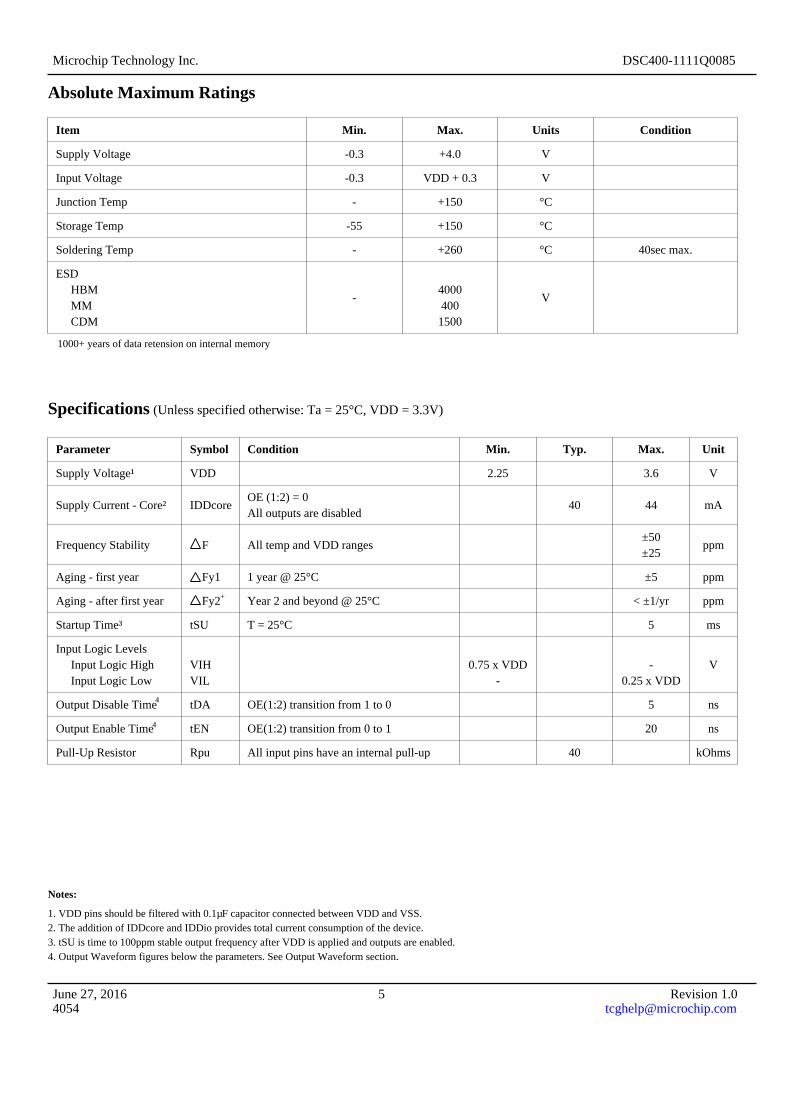
Absolute Maximum Ratings
Item Min. Max. Units Condition
Supply Voltage -0.3 +4.0 V
Input Voltage -0.3 VDD + 0.3 V
Junction Temp - +150 °C
Storage Temp -55 +150 °C
Soldering Temp - +260 °C 40sec max.
ESD HBM MM CDM
-40004001500
V
1000+ years of data retension on internal memory
Specifications (Unless specified otherwise: Ta = 25°C, VDD = 3.3V)
4
4
+
Parameter Symbol Condition Min. Typ. Max. Unit
Supply Voltage¹ VDD 2.25 3.6 V
Supply Current - Core² IDDcoreOE (1:2) = 0All outputs are disabled
40 44 mA
Frequency Stability F All temp and VDD ranges±50±25
ppm
Aging - first year Fy1 1 year @ 25°C ±5 ppm
Aging - after first year Fy2 Year 2 and beyond @ 25°C < ±1/yr ppm
Startup Time³ tSU T = 25°C 5 ms
Input Logic Levels Input Logic High Input Logic Low
VIHVIL
0.75 x VDD-
-0.25 x VDD
V
Output Disable Time tDA OE(1:2) transition from 1 to 0 5 ns
Output Enable Time tEN OE(1:2) transition from 0 to 1 20 ns
Pull-Up Resistor Rpu All input pins have an internal pull-up 40 kOhms
Notes:
1. VDD pins should be filtered with 0.1µF capacitor connected between VDD and VSS.2. The addition of IDDcore and IDDio provides total current consumption of the device.3. tSU is time to 100ppm stable output frequency after VDD is applied and outputs are enabled.4. Output Waveform figures below the parameters. See Output Waveform section.
June 27, 2016 5 Revision [email protected]

Microchip Technology Inc. DSC400-1111Q0085
LVCMOS Outputs
Output Logic Levels Output Logic High Output Logic Low
VOHVOL
I = ±6mA 0.9 x VDD-
-0.1 x VDD
V
Output Transition Time³ Rise Time Fall Time
tRtF
20% to 80%CL = 15pF
1.11.3
22
ns
Frequency
f1f2f3f4
CLK1CLK2CLK3CLK4
252525125
MHz
Output Duty Cycle SYM Differential 45 55 %
Supply Current - IO² IDDio Per output at 125MHz, CL = 15pF 11 14 mA
Period Jitter JPER CLK(1:4) = 125MHz 3 psRMS
Integrated Phase Noise JPH200kHz to 20MHz @ 156.25MHz100kHz to 20MHz @ 156.25MHz12kHz to 20MHz @ 156.25MHz
0.30.381.7 2
psRMS
LVCMOS Typical Termination Scheme
SR is a series resistor implemented to match the trace impedance to that of the clock output. Depending on the board layout,the value may range from 0 to 27Ohms.
LVCMOS Output Waveform
June 27, 2016 6 Revision [email protected]

Microchip Technology Inc. DSC400-1111Q0085
Connection Diagram
The connection Diagram below includes recommended capacitors to be placed on each VDD for noise filtering.
June 27, 2016 7 Revision [email protected]

Microchip Technology Inc. DSC400-1111Q0085
Solder Reflow Profile
MSL 1 @ 260°C refer to JSTD-020C
Ramp-Up Rate (200°C to Peak Temp) 3°C/sec Max.
Preheat Time 150°C to 200°C 60 - 180 sec
Time maintained above 217°C 60 - 150 sec
Peak Temperature 255 - 260°C
Time within 5°C of actual Peak 20 - 40 sec
Ramp-Down Rate 6°C/sec Max.
Time 25°C to Peak Temperature 8 min Max.
June 27, 2016 8 Revision [email protected]

Microchip Technology Inc. DSC400-1111Q0085
Package Information
20 QFN, 5.0mm x 3.2mm Package
June 27, 2016 9 Revision [email protected]

Microchip Technology Inc. DSC400-1111Q0085
Recommended Solder Pad layout
units: mm[inches]
Connect the center pad to ground plane for best thermal performance.
Microchip makes no representations or warranties with respect to the accuracy or completeness of the information furnished in this datasheet. This information is not intended as a warranty and Microchip does not assume responsibility for its use. Microchip reserves the right
to change circuitry, specifications and descriptions at any time without notice. No license, whether express, implied, arising byestoppel or otherwise, to any intellectual property rights is granted by this document. Except as provided in Microchip's terms and
conditions of sale for such products, Microchip assumes no liability whatsoever, and Microchip disclaims any express or implied warrantyrelating to the sale and/or use of Microchip products including liability or warranties relating to fitness for a particular purpose,
merchantability, or infringement of any patent, copyright or other intellectual property right.
Microchip products are not designed or authorized for use as components in life support appliances, devices or systems where malfunctionof a product can reasonably be expected to result in personal injury. Life support devices or systems are devices or systems that (a)
are intended for surgical implant into the body or (b) support or sustain life, and whose failure to perform can be reasonably expectedto result in a significant injury to the user. A Purchaser's use or sale of Microchip Products for use in life support appliances, devices
or systems is a Purchaser's own risk and Purchaser agrees to fully indemnify Microchip for any damages resulting from such use or sale.
© 2016 Microchip Technology Inc.
June 27, 2016 10 Revision [email protected]


