8-pin Flash PIC CHAPTER 1 8-Pin Flash PIC Microcontrollers...
16
© 2008 Microchip Technology Inc. Page 1-1 8-pin Flash PIC ® Microcontroller Tips ‘n Tricks CHAPTER 1 8-Pin Flash PIC ® Microcontrollers Tips ‘n Tricks Table Of Contents TIPS ‘N TRICKS WITH HARDWARE TIP #1: Dual Speed RC Oscillator ................ 1-2 TIP #2: Input/Output Multiplexing.................. 1-2 TIP #3: Read Three States From One Pin .... 1-3 TIP #4: Reading DIP Switches...................... 1-3 TIP #5: Scanning Many Keys With One Input.......................................... 1-4 TIP #6: Scanning Many Keys and Wake-up From Sleep ....................................... 1-4 TIP #7: 8x8 Keyboard with 1 Input ................ 1-5 TIP #8: One Pin Power/Data......................... 1-5 TIP #9: Decode Keys and ID Settings .......... 1-6 TIP #10: Generating High Voltages ................ 1-6 TIP #11: VDD Self Starting Circuit.................... 1-7 TIP #12: Using PIC ® MCU A/D For Smart Current Limiter.................................. 1-7 TIP #13: Reading A Sensor With Higher Accuracy........................................... 1-8 TIP #13.1: Reading A Sensor With Higher Accuracy – RC Timing Method ......... 1-8 TIP #13.2: Reading A Sensor With Higher Accuracy – Charge Balancing Method ............................................. 1-10 TIP #13.3: Reading A Sensor With Higher Accuracy – A/D Method .................... 1-11 TIP #14: Delta Sigma Converter ..................... 1-11 TIPS ‘N TRICKS WITH SOFTWARE TIP #15: Delay Techniques ............................. 1-12 TIP #16: Optimizing Destinations.................... 1-13 TIP #17: Conditional Bit Set/Clear .................. 1-13 TIP #18: Swap File Register with W ............... 1-14 TIP #19: Bit Shifting Using Carry Bit ............... 1-14 TIPS ‘N TRICKS INTRODUCTION Microchip continues to provide innovative products that are smaller, faster, easier to use and more reliable. The 8-pin Flash PIC ® microcontrollers (MCU) are used in an wide range of everyday products, from toothbrushes, hair dryers and rice cookers to industrial, automotive and medical products. The PIC12F629/675 MCUs merge all the advantages of the PIC MCU architecture and the flexibility of Flash program memory into an 8-pin package. They provide the features and intelligence not previously available due to cost and board space limitations. Features include a 14-bit instruction set, small footprint package, a wide operating voltage of 2.0 to 5.5 volts, an internal programmable 4 MHz oscillator, on-board EEPROM data memory, on-chip voltage reference and up to 4 channels of 10-bit A/D. The flexibility of Flash and an excellent development tool suite, including a low-cost In-Circuit Debugger, In-Circuit Serial Programming™ and MPLAB ® ICE 2000 emulation, make these devices ideal for just about any embedded control application. TIPS ‘N TRICKS WITH HARDWARE The following series of Tips ’n Tricks can be applied to a variety of applications to help make the most of the 8-pin dynamics.
Transcript of 8-pin Flash PIC CHAPTER 1 8-Pin Flash PIC Microcontrollers...

© 2008 Microchip Technology Inc. Page 1-1
8-pin Flash PIC® Microcontroller Tips ‘n Tricks
CHAPTER 18-Pin Flash PIC® Microcontrollers
Tips ‘n Tricks
Table Of Contents
TIPS ‘N TRICKS WITH HARDWARETIP #1: Dual Speed RC Oscillator ................ 1-2TIP #2: Input/Output Multiplexing .................. 1-2TIP #3: Read Three States From One Pin .... 1-3TIP #4: Reading DIP Switches ...................... 1-3TIP #5: Scanning Many Keys With One Input .......................................... 1-4TIP #6: Scanning Many Keys and Wake-up From Sleep ....................................... 1-4TIP #7: 8x8 Keyboard with 1 Input ................ 1-5TIP #8: One Pin Power/Data ......................... 1-5TIP #9: Decode Keys and ID Settings .......... 1-6TIP #10: Generating High Voltages ................ 1-6TIP #11: VDD Self Starting Circuit.................... 1-7TIP #12: Using PIC® MCU A/D For Smart Current Limiter .................................. 1-7TIP #13: Reading A Sensor With Higher Accuracy ........................................... 1-8TIP #13.1: Reading A Sensor With Higher Accuracy – RC Timing Method ......... 1-8TIP #13.2: Reading A Sensor With Higher Accuracy – Charge Balancing Method ............................................. 1-10TIP #13.3: Reading A Sensor With Higher Accuracy – A/D Method .................... 1-11TIP #14: Delta Sigma Converter ..................... 1-11
TIPS ‘N TRICKS WITH SOFTWARETIP #15: Delay Techniques ............................. 1-12TIP #16: Optimizing Destinations .................... 1-13TIP #17: Conditional Bit Set/Clear .................. 1-13TIP #18: Swap File Register with W ............... 1-14TIP #19: Bit Shifting Using Carry Bit ............... 1-14
TIPS ‘N TRICKS INTRODUCTIONMicrochip continues to provide innovative products that are smaller, faster, easier to use and more reliable. The 8-pin Flash PIC® microcontrollers (MCU) are used in an wide range of everyday products, from toothbrushes, hair dryers and rice cookers to industrial, automotive and medical products.The PIC12F629/675 MCUs merge all the advantages of the PIC MCU architecture and the fl exibility of Flash program memory into an 8-pin package. They provide the features and intelligence not previously available due to cost and board space limitations. Features include a 14-bit instruction set, small footprint package, a wide operating voltage of 2.0 to 5.5 volts, an internal programmable 4 MHz oscillator, on-board EEPROM data memory, on-chip voltage reference and up to 4 channels of 10-bit A/D. The fl exibility of Flash and an excellent development tool suite, including a low-cost In-Circuit Debugger, In-Circuit Serial Programming™ and MPLAB® ICE 2000 emulation, make these devices ideal for just about any embedded control application.
TIPS ‘N TRICKS WITH HARDWAREThe following series of Tips ’n Tricks can be applied to a variety of applications to help make the most of the 8-pin dynamics.

© 2008 Microchip Technology Inc.Page 1-2
8-pin Flash PIC® Microcontroller Tips ‘n Tricks
TIP #1 Dual Speed RC OscillatorFigure 1-1
PIC12F6XX
OSC1
GP0
+5V
R2R1
C
1. After reset I/O pin is High-Z2. Output ‘1’ on I/O pin3. R1, R2 and C determine OSC frequency4. Also works with additional capacitorsFrequency of PIC MCU in external RC oscillator mode depends on resistance and capacitance on OSC1 pin. Resistance is changed by the output voltage on GP0. GP0 output ‘1’ puts R2 in parallel with R1 reduces OSC1 resistance and increases OSC1 frequency. GP0 as an input increases the OSC1 resistance by minimizing current fl ow through R2, and decreases frequency and power consumption.
Summary:GP0 = Input: Slow speed for low currentGP0 = Output high: High speed for fast processing
TIP #2 Input/Output MultiplexingIndividual diodes and some combination of diodes can be enabled by driving I/Os high and low or switching to inputs (Z). The number of diodes (D) that can be controlled depends on the number of I/Os (GP) used.The equation is: D = GP x (GP - 1).
Example 2-1: Six LEDs on Three I/O Pins
GPx LEDs0 1 2
0 0 00 1 Z1 0 ZZ 0 1Z 1 00 Z 11 Z 00 0 10 1 00 1 11 0 01 0 11 1 01 1 1
1 2 3 4 5 6
0 0 0 0 0 01 0 0 0 0 00 1 0 0 0 00 0 1 0 0 00 0 0 1 0 00 0 0 0 1 00 0 0 0 0 10 0 1 0 1 01 0 0 1 0 01 0 0 0 1 00 1 0 0 0 10 1 1 0 0 00 0 0 1 0 10 0 0 0 0 0
Figure 2-1
PIC12F6XX
1 2 5
43
6
GP0
GP1
GP2

© 2008 Microchip Technology Inc. Page 1-3
8-pin Flash PIC® Microcontroller Tips ‘n Tricks
TIP #3 Read Three States From One PinTo check state Z:• Drive output pin high• Set to Input• Read 1• Drive output pin low• Set to Input• Read 0To check state 0:• Read 0 on pin
To check state 1:• Read 1 on pin
State Link 0 Link 10 closed open1 open closed
NC open open
Jumper has three possible states: not connected, Link 1 and Link 0. The capacitor will charge and discharge depending on the I/O output voltage allowing the “not connected” state. Software should check the “not connected” state fi rst by driving I/O high, reading 1 and driving I/O low and reading 0. The “Link 1” and “Link 0” states are read directly.
PICI/O
5V
0V
Link 0
Link 1
Figure 3-1
TIP #4 Reading DIP SwitchesThe input of a timer can be used to test which switch(s) is closed. The input of Timer1 is held high with a pull-up resistor. Sequentially, each switch I/O is set to input and Timer1 is checked for an increment indicating the switch is closed.Each bit in the DP register represents its corresponding switch position. By setting Timer1 to FFFFh and enabling its interrupt, an increment will cause a rollover and generate an interrupt. This will simplify the software by eliminating the bit test on the TMR1L register.Sequentially set each GPIO to an input and test for TMR1 increment (or 0 if standard I/O pin is used).
Figure 4-1
PIC12F6XX
GP0GP1GP2GP3
GP5/T1CKI10K
VDD
GP4Data I/O
movlw b'11111111'movwf TRISIOmovwf DIPmovlw b'00000111'movwf T1CONmovlw b'11111110'movwf Maskclrf GPIO
LOOPclrf TMR1Lmovf Mask,Wmovwf TRISIObtfsc TMR1L,0andwf DIP,Fbsf STATUS,Crlf Mask,Fbtfsc Mask,4goto Loopretlw 0
Example 4-1

© 2008 Microchip Technology Inc.Page 1-4
8-pin Flash PIC® Microcontroller Tips ‘n Tricks
TIP #5 Scanning Many Keys With One InputThe time required to charge a capacitor depends on resistance between VDD and capacitor. When a button is pressed, VDD is supplied to a different point in the resistor ladder. The resistance between VDD and the capacitor is reduced, which reduces the charge time of the capacitor. A timer is used with a comparator or changing digital input to measure the capacitor charge time. The charge time is used to determine which button is pressed.Software sequence:1. Confi gure GP2 to output a low voltage to discharge capacitor through I/O resistor.2. Confi gure GP2 as one comparator input and CVr ef as the other.3. Use a timer to measure when the comparator trips. If the time measured is greater than the maximum allowed time, then repeat; otherwise determine which button is pressed.When a key is pressed, the voltage divider network changes the RC ramp rate.
Figure 5-1
PIC12F6XX
GP0GP1
GP2
GP4GP5
GP3
16Resistors
220Ω
R
R
R
R
See AN512, “Implementing Ohmmeter/ Temperature Sensor” for code ideas.
TIP #6 Scanning Many Keys and Wake-up From SleepAn additional I/O can be added to wake the part when a button is pressed. Prior to Sleep, confi gure GP1 as an input with interrupt-on-change enabled and GP2 to output high. The pull-down resistor holds GP1 low until a button is pressed. GP1 is then pulled high via GP2 and VDD generating an interrupt. After wake-up, GP2 is confi gured to output low to discharge the capacitor through the 220Ω resistor. GP1 is set to output high and GP2 is set to an input to measure the capacitor charge time.• GP1 pin connected to key common• Enable wake-up on port change• Set GP1 as input and GP2 high prior to Sleep• If key is pressed the PIC MCU wakes up, GP2 must be set low to discharge capacitor• Set GP1 high upon wake-up to scan keystroke
Figure 6-1
VDD100R
PIC12F6XX
GP0GP1
GP2
GP4GP5
GP3220Ω
R
R
R
R
16Resistors

© 2008 Microchip Technology Inc. Page 1-5
8-pin Flash PIC® Microcontroller Tips ‘n Tricks
TIP #7 4x4 Keyboard with 1 InputBy carefully selecting the resistor values, each button generates a unique voltage. This voltage is measured by the A/D to determine which button is pressed. Higher precision resistors should be used to maximize voltage uniqueness. The A/D will read near 0 when no buttons are pressed.
Figure 7-1
VDD
PIC12F6XX
GP0
TIP #8 One Pin Power/DataA single I/O can be used for both a single-direction communication and the power source for another microcontroller. The I/O line is held high by the pull-up resistor connected to VDD. The sender uses a pull-down transistor to pull the data line low or disables the transistor to allow the pull-up to raise it to send data to the receiver. VDD is supplied to the sender through the data line. The capacitor stabilizes the sender’sVDD and a diode prevents the capacitor from discharging through the I/O line while it is low. Note that the VDD of the sender is a diode-drop lower than the receiver.
Figure 8-1
VDD VDD
Receiver
GP0 GP0
Sender
VDD - 0.7V

© 2008 Microchip Technology Inc.Page 1-6
8-pin Flash PIC® Microcontroller Tips ‘n Tricks
TIP #9 Decode Keys and ID SettingsButtons and jumpers can share I/O’s by using another I/O to select which one is read. Both buttons and jumpers are tied to a shared pull-down resistor. Therefore, they will read as ‘0’ unless a button is pressed or a jumper is connected. Each input (GP3/2/1/0) shares a jumper and a button. To read the jumper settings, set GP4 to output high and each connected jumper will read as ‘1’ on its assigned I/O or ‘0’ if it’s not connected. With GP4 output low, a pressed button will be read as ‘1’ on its assigned I/O and ‘0’ otherwise.
Figure 9-1
VDD
GP0GP1GP2GP3GP4
• When GP4 = 1 and no keys are pressed, read ID setting• When GP4 = 0, read the switch buttons
TIP #10 Generating High VoltagesFigure 10-1
PIC12F6XXw/RC CLKOUT
CPUMP CFILTER
CLKOUTVOUT max = 2 * VDD - 2 * VDIODE
VDD
Voltages greater than VDD can be generated using a toggling I/O. PIC MCUs CLKOUT/OSC2 pin toggles at one quarter the frequency of OSC1 when in external RC oscillator mode. When OSC2 is low, the VDD diode is forward biased and conducts current, thereby charging CPUMP. After OSC2 is high, the other diode is forward biased, moving the charge to CFILTER. The result is a charge equal to twice the VDD minus two diode drops. This can be used with a PWM, a toggling I/O or other toggling pin.

© 2008 Microchip Technology Inc. Page 1-7
8-pin Flash PIC® Microcontroller Tips ‘n Tricks
TIP #11 VDD Self Starting CircuitBuilding on the previous topic, the same charge pump can be used by the MCU to supply its own VDD. Before the switch is pressed, VBAT has power and the VDD points are connected together but unpowered. When the button is pressed, power is supplied to VDD and the MCUs CLKOUT (in external RC oscillator mode) begins toggle. The voltage generated by the charge pump turns on the FET allowing VDD to remain powered. To power down the MCU, execute a Sleep instruction. This allows the MCU to switch off its power source via software.
Advantages:• PIC MCU leakage current nearly 0• Low cost (uses n-channel FET)• Reliable• No additional I/O pins required
Figure 11-1
PIC12F6XX
CLKOUT
VDD
VDD
VDD
VBAT
VDD
TIP #12 Using PIC® MCU A/D For Smart Current LimiterFigure 12-1
W
PIC12F6XX
10KAN0
RSENSE
Load or Motor
• Detect current through low side sense resistor• Optional peak fi lter capacitor• Varying levels of overcurrent response can be realized in softwareBy adding a resistor (RSENSE) in series with a motor, the A/D can be used to measure in-rush current, provide current limiting, over-current recovery or work as a smart circuit breaker. The 10K resistor limits the analog channel current and does not violate the source impedance limit of the A/D.

© 2008 Microchip Technology Inc.Page 1-8
8-pin Flash PIC® Microcontroller Tips ‘n Tricks
Tip #13.1 Reading a Sensor With Higher Accuracy – RC Timing Method
RC Timing Method:Simple RC step responseVc(t) = VDD * (1 - e -t/(RC))t = -RC ln(1 - VTH/VDD)VTH/VDD is constantR2 = (t2/t1) * R1
Figure 13-1
Time
Vc(t)
VTH
t = 0 t = t1 t = t2
R1 R2
A reference resistor can be used to improve the accuracy of an analog sensor reading. In this diagram, the charge time of a resistor/capacitor combination is measured using a timer and a port input or comparator input switches from a ‘0’ to ‘1’. The R1 curve uses a reference resistor and the R2 curve uses the sensor. The charge time of the R1 curve is known and can be used to calibrate the unknown sensor reading, R2. This reduces the affects of temperature, component tolerance and noise while reading the sensor.
TIP #13 Reading a Sensor With Higher AccuracySensors can be read directly with the A/D but in some applications, factors such as temperature, external component accuracy, sensor non-linearity and/or decreasing battery voltage need to be considered. In other applications, more than 10 bits of accuracy are needed and a slower sensor read is acceptable. The following tips deal with these factors and show how to get the most out of a PIC MCU.
13.1. RC Timing Method (with reference resistor)13.2. Charge Balancing Method13.3. A/D Method

© 2008 Microchip Technology Inc. Page 1-9
8-pin Flash PIC® Microcontroller Tips ‘n Tricks
1. Set GP1 and GP2 to inputs, and GP0 to a low output to discharge C2. Set GP0 to an input and GP1 to a high output3. Measure tRSEN (GP0 changes to 1)4. Repeat step 15. Set GP0 to an input and GP2 to a high output6. Measure tRREF (GP0 changes to 1)7. Use fi lm polypropylene capacitor8. RTH = x RREF tRSEN
tRREF
Figure 13-2
PIC12F629
GP0
GP1
GP2RREF
RSEN
Other alternatives: voltage comparator in the PIC12F6XX to measure capacitor voltage on GP0.
Application Notes:AN512, “Implementing Ohmmeter/Temperature Sensor”AN611, “Resistance and Capacitance Meter Using a PIC16C622”Here is the schematic and software fl ow for using a reference resistor to improve the accuracy of an analog sensor reading. The reference resistor (RREF) and sensor (RSEN) are assigned an I/O and share a common capacitor. GP0 is used to discharge the capacitor and represents the capacitor voltage.Through software, a timer is used to measure when GP0 switches from a ‘0’ to a ‘1’ for the sensor and reference measurements. Any difference measured between the reference measurement and its calibrated measurement is used to adjust the sensor reading, resulting in a more accurate measurement.The comparator and comparator reference on the PIC12F629/675 can be used instead of a port pin for a more accurate measurement. Polypropylene capacitors are very stable and benefi cial in this type of application.

© 2008 Microchip Technology Inc.Page 1-10
8-pin Flash PIC® Microcontroller Tips ‘n Tricks
The comparator and comparator voltage reference (CVREF) on the PIC12F629/675 are ideal for this application.1. GP1 average voltage = CVREF
2. Time base as sampling rate3. At the end of each time base period: - If GP1 > CVREF, then GP2 Output Low - If GP1 < CVREF, then GP2 Input mode4. Accumulate the GP2 lows over many samples5. Number of samples determines resolution6. Number of GP2 lows determine effective duty cycle of Rr ef
Figure 13-3
PIC12F6XX
RSEN
GP1
GP2
T1GRREF
VDD
+
-
CVREF
COUT
Tip #13.2 Reading a Sensor With Higher Accuracy – Charge Balancing Method1. Sensor charges a capacitor2. Reference resistor discharges the capacitor3. Modulate reference resistor to maintain constant average charge in the capacitor4. Use comparator to determine modulationTo improve resolution beyond 10 or 12 bits, a technique called “Charge Balancing” can be used. The basic concept is for the MCU to maintain a constant voltage on a capacitor by either allowing the charge to build through a sensor or discharge through a reference resistor. A timer is used to sample the capacitor voltage on regular intervals until a predetermined number of samples are counted. By counting the number of times the capacitor voltage is over an arbitrary threshold, the sensor voltage is determined.

© 2008 Microchip Technology Inc. Page 1-11
8-pin Flash PIC® Microcontroller Tips ‘n Tricks
TIP #14 Delta-Sigma ConverterThe charge on the capacitor on GP1 is maintained about equal to the CVREF by the MCU monitoring COUT and switching GP2 from Input mode or output low appropriately. A timer is used to sample the COUT bit on a periodic basis. Each time GP2 is driven low, a counter is incremented. This counter value corresponds to the input voltage.To minimize the affects of external component tolerances, temperature, etc., the circuit can be calibrated. Apply a known voltage to the input and allow the microcontroller to count samples until the expected result is calculated. By taking the same number of samples for subsequent measurements, they become calibrated measurements.
Figure 14-1
COUT
VIN
CVREF
PIC12F6XX
GP1
GP2
+
-
1. GP1 average voltage = CVREF
2. Time base as sampling rate3. At the end of each time base period: - If GP1 > CVREF, then GP2 Output Low - If GP1 < CVREF, then GP2 Output High4. Accumulate the GP2 lows over many samples5. Number of samples determines resolution
Tip #13.3 Reading a Sensor With Higher Accuracy – A/D MethodNTC (Negative Temperature Coeffi cient) sensors have a non-linear response to temperature changes. As the temperature drops, the amount the resistance changes becomes less and less. Such sensors have a limited useful range because the resolution becomes smaller than the A/D resolution as the temperature drops. By changing the voltage divider of the RSEN, the temperature range can be expanded.To select the higher temperature range, GP1 outputs ‘1’ and GP2 is set as an input. For the lower range, GP2 outputs ‘1’ and GP1 is confi gured as an input. The lower range will increase the amount the sensor voltage changes as the temperature drops to allow a larger usable sensor range.
Summary:High range: GP1 output ‘1’ and GP2 inputLow range: GP1 input and GP2 output ‘1’1. 10K and 100K resistors are used to set the range2. Vr ef for A/D = Vdd3. Rth calculation is independent of Vdd4. Count = Rsen/(Rsen+Rr ef ) x 2555. Don’t forget to allow acquisition time for the A/D
Figure 13-4
PIC12F675
AN0 (A/D Input)
GP1
GP2100K
10K
RSEN
© 2008 Microchip Technology Inc.Page 1-12
8-pin Flash PIC® Microcontroller Tips ‘n Tricks
TIPS ‘N TRICKS WITH SOFTWARETo reduce costs, designers need to make the most of the available program memory in MCUs. Program memory is typically a large portion of the MCU cost. Optimizing the code helps to avoid buying more memory than needed. Here are some ideas that can help reduce code size.
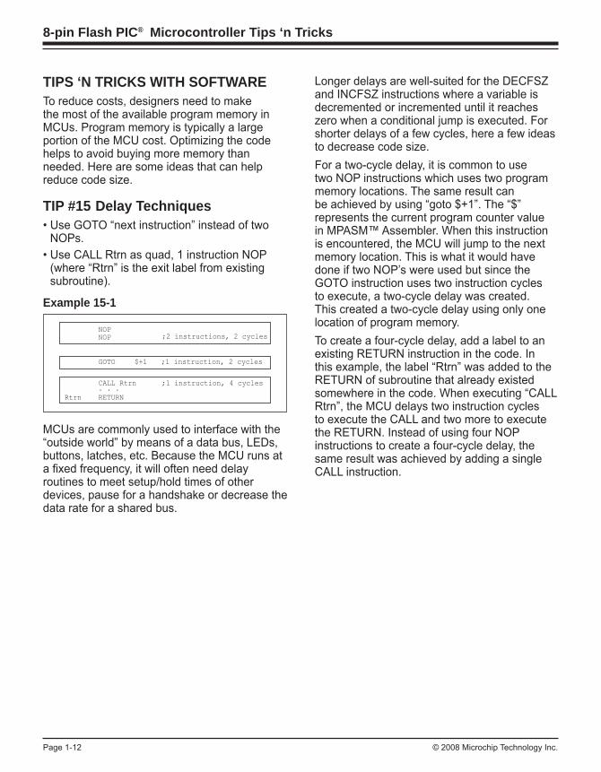
TIP #15 Delay Techniques• Use GOTO “next instruction” instead of two NOPs.• Use CALL Rtrn as quad, 1 instruction NOP (where “Rtrn” is the exit label from existing subroutine).
Example 15-1
NOPNOP
GOTO $+1
CALL Rtrn ;1 instruction, 4 cycles
Rtrn RETURN. . .
;2 instructions, 2 cycles
;1 instruction, 2 cycles
MCUs are commonly used to interface with the “outside world” by means of a data bus, LEDs, buttons, latches, etc. Because the MCU runs at a fi xed frequency, it will often need delay routines to meet setup/hold times of other devices, pause for a handshake or decrease the data rate for a shared bus.
Longer delays are well-suited for the DECFSZ and INCFSZ instructions where a variable is decremented or incremented until it reaches zero when a conditional jump is executed. For shorter delays of a few cycles, here a few ideas to decrease code size.For a two-cycle delay, it is common to usetwo NOP instructions which uses two program memory locations. The same result can be achieved by using “goto $+1”. The “$” represents the current program counter value in MPASM™ Assembler. When this instruction is encountered, the MCU will jump to the next memory location. This is what it would have done if two NOP’s were used but since the GOTO instruction uses two instruction cycles to execute, a two-cycle delay was created. This created a two-cycle delay using only one location of program memory.To create a four-cycle delay, add a label to an existing RETURN instruction in the code. In this example, the label “Rtrn” was added to the RETURN of subroutine that already existed somewhere in the code. When executing “CALL Rtrn”, the MCU delays two instruction cycles to execute the CALL and two more to execute the RETURN. Instead of using four NOP instructions to create a four-cycle delay, the same result was achieved by adding a single CALL instruction.

© 2008 Microchip Technology Inc. Page 1-13
8-pin Flash PIC® Microcontroller Tips ‘n Tricks
TIP #16 Optimizing Destinations• Destination bit determines W for F for result• Look at data movement and restructure
Example 16-1
Example: A + B → A
MOVFADDWFMOVWF
MOVFADDWF
A,WB,WA
B,WA,F
3 instructions 2 instructions
Careful use of the destination bits in instructions can save program memory. Here, register A and register B are summed and the result is put into the A register. A destination option is available for logic and arithmetic operations. In the fi rst example, the result of the ADDWF instruction is placed in the working register. A MOVWF instruction is used to move the result from the working register to register A. In the second example, the ADDWF instruction uses the destination bit to place the result into the A register, saving an instruction.
TIP #17 Conditional Bit Set/Clear• To move single bit of data from REGA to REGB• Precondition REGB bit• Test REGA bit and fi x REGB if necessary
Example 17-1
BTFSSBCFBTFSCBSF
BCFBTFSCBSF
REGA,2REGB,5REGA,2REGB,5
REGB,5REGA,2REGB,5
4 instructions 3 instructions
One technique for moving one bit from the REGA register to REGB is to perform bit tests. In the fi rst example, the bit in REGA is tested using a BTFSS instruction. If the bit is clear, the BCF instruction is executed and clears the REGB bit, and if the bit is set, the instruction is skipped.The second bit test determines if the bit is set, and if so, will execute the BSF and set the REGB bit, otherwise the instruction is skipped. This sequence requires four instructions.A more effi cient technique is to assume the bit in REGA is clear, and clear the REGB bit, and test if the REGA bit is clear. If so, the assumption was correct and the BSF instruction is skipped, otherwise the REGB bit is set. The sequence in the second example uses three instructions because one bit test was not needed.One important point is that the second example will create a two-cycle glitch if REGB is a port outputting a high. This is caused by the BCF and BTFSC instructions that will be executed regardless of the bit value in REGA.

© 2008 Microchip Technology Inc.Page 1-14
8-pin Flash PIC® Microcontroller Tips ‘n Tricks
TIP #18 Swap File Register with WExample 18-1
SWAPWF MACRO REGXORWF REG,FXORWF REG,WXORWF REG,FENDM
The following macro swaps the contents of W and REG without using a second register.Needs: 0 TEMP registers 3 Instructions 3 TCYAn effi cient way of swapping the contents of a register with the working register is to use three XORWF instructions. It requires no temporary registers and three instructions. Here’s an example: W REG Instruction10101100 01011100 XORWF REG,F10101100 11110000 XORWF REG,W01011100 11110000 XORWF REG,F01011100 10101100 Result
TIP #19 Bit Shifting Using Carry BitRotate a byte through carry without using RAM variable for loop count:• Easily adapted to serial interface transmit routines.• Carry bit is cleared (except last cycle) and the cycle repeats until the zero bit sets indicating the end.
Example 19-1
bsfrlfbcfbtfscbsfbcfrlfmovfbtfssgoto
LIST P=PIC12f629INCLUDE P12f629.INCbuffer
STATUS,C buffer,f GPIO,Dout STATUS,C GPIO,Dout STATUS,C buffer,f buffer,f STATUS,Z Send_Loop
equ 0x20
;Set 'end of loop' flag ;Place first bit into C ;precondition output ;Check data 0 or 1 ?
;Clear data in C ;Place next bit into C ;Force Z bit ;Exit?

© 2008 Microchip Technology Inc.
Tips ‘n Tricks
NOTES:

Microchip Technology Inc. • 2355 W. Chandler Blvd. • Chandler, AZ 85224-6199www.microchip.com
AMERICAS
Atlanta
Tel: 678-957-9614Boston
Tel: 774-760-0087Chicago
Tel: 630-285-0071Cleveland
Tel: 216-447-0464Dallas
Tel: 972-818-7423Detroit
Tel: 248-538-2250Kokomo
Tel: 765-864-8360Los Angeles
Tel: 949-462-9523Santa Clara
Tel: 408-961-6444Toronto
Mississauga, OntarioTel: 905-673-0699
EUROPE
Austria - Wels
Tel: 43-7242-2244-39Denmark - Copenhagen
Tel: 45-4450-2828France - Paris
Tel: 33-1-69-53-63-20Germany - Munich
Tel: 49-89-627-144-0Italy - Milan
Tel: 39-0331-742611Netherlands - Drunen
Tel: 31-416-690399Spain - Madrid
Tel: 34-91-708-08-90UK - Wokingham
Tel: 44-118-921-5869
ASIA/PACIFIC
Australia - Sydney
Tel: 61-2-9868-6733China - Beijing
Tel: 86-10-8528-2100China - Chengdu
Tel: 86-28-8665-5511China - Hong Kong SAR
Tel: 852-2401-1200China - Nanjing
Tel: 86-25-8473-2460China - Qingdao
Tel: 86-532-8502-7355China - Shanghai
Tel: 86-21-5407-5533China - Shenyang
Tel: 86-24-2334-2829China - Shenzhen
Tel: 86-755-8203-2660China - Wuhan
Tel: 86-27-5980-5300China - Xiamen
Tel: 86-592-2388138China - Xian
Tel: 86-29-8833-7252China - Zhuhai
Tel: 86-756-3210040
ASIA/PACIFIC
India - Bangalore
Tel: 91-80-4182-8400India - New Delhi
Tel: 91-11-4160-8631India - Pune
Tel: 91-20-2566-1512Japan - Yokohama
Tel: 81-45-471- 6166Korea - Daegu
Tel: 82-53-744-4301Korea - Seoul
Tel: 82-2-554-7200Malaysia - Kuala Lumpur
Tel: 60-3-6201-9857Malaysia - Penang
Tel: 60-4-227-8870Philippines - Manila
Tel: 63-2-634-9065Singapore
Tel: 65-6334-8870Taiwan - Hsin Chu
Tel: 886-3-572-9526Taiwan - Kaohsiung
Tel: 886-7-536-4818Taiwan - Taipei
Tel: 886-2-2500-6610Thailand - Bangkok
Tel: 66-2-694-13511/30/07
Sales Office Listing
Information subject to change. The Microchip name and logo, the Microchip logo, dsPIC, MPLAB, PIC, PICmicro and PICSTART are registered trademarks of Microchip Technology Incorporated in the U.S.A. and other countries. FilterLab, MXDEV and MXLAB are registered trademarks of Microchip Technology Incorporated in the U.S.A. ICSP, MPASM, MPLIB, MPLINK, PICkit, PICDEM, PICDEM.net and PICtail are trademarks of Microchip Technology Incorporated in the U.S.A. and other countries. SQTP is a service mark of Microchip Technology Incorporated in the U.S.A. All other trademarks mentioned herein are property of their respective companies. © 2008, Microchip Technology Incorporated. All Rights Reserved. Printed in the U.S.A. 2/08